JP2020514810A - Free-form surface prism and head-mounted display with magnified field of view - Google Patents
Free-form surface prism and head-mounted display with magnified field of view Download PDFInfo
- Publication number
- JP2020514810A JP2020514810A JP2019548958A JP2019548958A JP2020514810A JP 2020514810 A JP2020514810 A JP 2020514810A JP 2019548958 A JP2019548958 A JP 2019548958A JP 2019548958 A JP2019548958 A JP 2019548958A JP 2020514810 A JP2020514810 A JP 2020514810A
- Authority
- JP
- Japan
- Prior art keywords
- free
- ini
- prism
- mounted display
- optical
- Prior art date
- Legal status (The legal status is an assumption and is not a legal conclusion. Google has not performed a legal analysis and makes no representation as to the accuracy of the status listed.)
- Pending
Links
- 238000003384 imaging method Methods 0.000 claims abstract description 38
- 239000002131 composite material Substances 0.000 claims abstract description 6
- 230000003287 optical effect Effects 0.000 claims description 123
- 210000001747 pupil Anatomy 0.000 claims description 21
- 239000011248 coating agent Substances 0.000 claims description 6
- 238000000576 coating method Methods 0.000 claims description 6
- 210000003128 head Anatomy 0.000 claims description 5
- 238000003491 array Methods 0.000 claims description 3
- 150000001875 compounds Chemical class 0.000 claims 1
- 238000010586 diagram Methods 0.000 abstract 1
- 238000013461 design Methods 0.000 description 18
- 208000013057 hereditary mucoepithelial dysplasia Diseases 0.000 description 14
- 238000012937 correction Methods 0.000 description 13
- 230000000007 visual effect Effects 0.000 description 13
- 238000000034 method Methods 0.000 description 9
- 238000005516 engineering process Methods 0.000 description 8
- 230000006870 function Effects 0.000 description 6
- 238000012546 transfer Methods 0.000 description 5
- 230000008447 perception Effects 0.000 description 4
- 230000004075 alteration Effects 0.000 description 3
- 230000000694 effects Effects 0.000 description 3
- 102100025222 CD63 antigen Human genes 0.000 description 2
- 101000934368 Homo sapiens CD63 antigen Proteins 0.000 description 2
- 206010052143 Ocular discomfort Diseases 0.000 description 2
- 230000004308 accommodation Effects 0.000 description 2
- 230000002350 accommodative effect Effects 0.000 description 2
- 230000003190 augmentative effect Effects 0.000 description 2
- 230000008901 benefit Effects 0.000 description 2
- 230000005540 biological transmission Effects 0.000 description 2
- 238000012938 design process Methods 0.000 description 2
- 230000004438 eyesight Effects 0.000 description 2
- 239000004973 liquid crystal related substance Substances 0.000 description 2
- 239000000463 material Substances 0.000 description 2
- 229920003229 poly(methyl methacrylate) Polymers 0.000 description 2
- 239000004926 polymethyl methacrylate Substances 0.000 description 2
- 230000005855 radiation Effects 0.000 description 2
- 230000004256 retinal image Effects 0.000 description 2
- 238000005070 sampling Methods 0.000 description 2
- 230000004304 visual acuity Effects 0.000 description 2
- 201000004964 Rhizomelic Chondrodysplasia Punctata Diseases 0.000 description 1
- 230000003044 adaptive effect Effects 0.000 description 1
- 238000013459 approach Methods 0.000 description 1
- 230000004888 barrier function Effects 0.000 description 1
- 230000000903 blocking effect Effects 0.000 description 1
- 230000015556 catabolic process Effects 0.000 description 1
- 230000008859 change Effects 0.000 description 1
- 238000006243 chemical reaction Methods 0.000 description 1
- 238000004891 communication Methods 0.000 description 1
- 230000001276 controlling effect Effects 0.000 description 1
- 230000007123 defense Effects 0.000 description 1
- 238000006731 degradation reaction Methods 0.000 description 1
- 238000011161 development Methods 0.000 description 1
- 238000000295 emission spectrum Methods 0.000 description 1
- 230000002349 favourable effect Effects 0.000 description 1
- 239000007788 liquid Substances 0.000 description 1
- 238000005457 optimization Methods 0.000 description 1
- 238000004806 packaging method and process Methods 0.000 description 1
- 230000009467 reduction Effects 0.000 description 1
- 230000001105 regulatory effect Effects 0.000 description 1
- 230000004044 response Effects 0.000 description 1
- 230000002207 retinal effect Effects 0.000 description 1
- 238000000926 separation method Methods 0.000 description 1
- 238000004088 simulation Methods 0.000 description 1
- 238000012549 training Methods 0.000 description 1
Images


Classifications
-
- G—PHYSICS
- G02—OPTICS
- G02B—OPTICAL ELEMENTS, SYSTEMS OR APPARATUS
- G02B27/00—Optical systems or apparatus not provided for by any of the groups G02B1/00 - G02B26/00, G02B30/00
- G02B27/0075—Optical systems or apparatus not provided for by any of the groups G02B1/00 - G02B26/00, G02B30/00 with means for altering, e.g. increasing, the depth of field or depth of focus
-
- G—PHYSICS
- G02—OPTICS
- G02B—OPTICAL ELEMENTS, SYSTEMS OR APPARATUS
- G02B17/00—Systems with reflecting surfaces, with or without refracting elements
- G02B17/08—Catadioptric systems
- G02B17/0856—Catadioptric systems comprising a refractive element with a reflective surface, the reflection taking place inside the element, e.g. Mangin mirrors
- G02B17/086—Catadioptric systems comprising a refractive element with a reflective surface, the reflection taking place inside the element, e.g. Mangin mirrors wherein the system is made of a single block of optical material, e.g. solid catadioptric systems
-
- G—PHYSICS
- G02—OPTICS
- G02B—OPTICAL ELEMENTS, SYSTEMS OR APPARATUS
- G02B25/00—Eyepieces; Magnifying glasses
- G02B25/001—Eyepieces
-
- G—PHYSICS
- G02—OPTICS
- G02B—OPTICAL ELEMENTS, SYSTEMS OR APPARATUS
- G02B27/00—Optical systems or apparatus not provided for by any of the groups G02B1/00 - G02B26/00, G02B30/00
- G02B27/01—Head-up displays
- G02B27/017—Head mounted
- G02B27/0172—Head mounted characterised by optical features
-
- G—PHYSICS
- G02—OPTICS
- G02B—OPTICAL ELEMENTS, SYSTEMS OR APPARATUS
- G02B3/00—Simple or compound lenses
- G02B3/0006—Arrays
-
- G—PHYSICS
- G02—OPTICS
- G02B—OPTICAL ELEMENTS, SYSTEMS OR APPARATUS
- G02B30/00—Optical systems or apparatus for producing three-dimensional [3D] effects, e.g. stereoscopic images
- G02B30/10—Optical systems or apparatus for producing three-dimensional [3D] effects, e.g. stereoscopic images using integral imaging methods
-
- G—PHYSICS
- G02—OPTICS
- G02B—OPTICAL ELEMENTS, SYSTEMS OR APPARATUS
- G02B5/00—Optical elements other than lenses
- G02B5/04—Prisms
-
- G—PHYSICS
- G02—OPTICS
- G02B—OPTICAL ELEMENTS, SYSTEMS OR APPARATUS
- G02B27/00—Optical systems or apparatus not provided for by any of the groups G02B1/00 - G02B26/00, G02B30/00
- G02B27/01—Head-up displays
- G02B27/0101—Head-up displays characterised by optical features
- G02B2027/0123—Head-up displays characterised by optical features comprising devices increasing the field of view
-
- G—PHYSICS
- G02—OPTICS
- G02B—OPTICAL ELEMENTS, SYSTEMS OR APPARATUS
- G02B27/00—Optical systems or apparatus not provided for by any of the groups G02B1/00 - G02B26/00, G02B30/00
- G02B27/01—Head-up displays
- G02B27/0101—Head-up displays characterised by optical features
- G02B2027/0127—Head-up displays characterised by optical features comprising devices increasing the depth of field
Landscapes
- Physics & Mathematics (AREA)
- General Physics & Mathematics (AREA)
- Optics & Photonics (AREA)
- Optical Elements Other Than Lenses (AREA)
- Microscoopes, Condenser (AREA)
- Stereoscopic And Panoramic Photography (AREA)
- Lenses (AREA)
Abstract
【解決手段】 複合表面を有する自由曲面導波路型プリズムおよびインテグラルイメージングおよびリレー群を用いたヘッドマウント・ライトフィールド・ディスプレイでの使用。【選択図】 図6CUse in free-form waveguide prisms with composite surfaces and head-mounted light-field displays using integral imaging and relay groups. [Selection diagram] FIG. 6C
Description
関連出願
本出願は、2017年3月9日付で出願された米国仮特許出願第62/469,104号明細書の優先権の利益を主張し、その出願の全内容は、この参照により本明細書に組み込まれる。
Related Application This application claims the benefit of priority of US Provisional Patent Application No. 62 / 469,104, filed March 9, 2017, the entire contents of which are hereby incorporated by reference. Incorporated into the book.
政府許認可権
本発明は、NSFによる認可を受けた登録番号1422653の下で政府の支援を受けて行われた。政府は、本発明において一定の権利を有する。
GOVERNMENT LICENSING RIGHTS This invention was made with government support under NSF-approved registration number 1422653. The government has certain rights in this invention.
本発明は、ヘッドマウントディスプレイの分野に関し、より具体的には、排他的にではないが、インテグラルイメージング(integral imaging:InI)に基づくヘッドマウントディスプレイに関する。 The present invention relates to the field of head mounted displays, and more particularly, but not exclusively, to head mounted displays based on integral imaging (InI).
ニアアイディスプレイ(near−to−eye display:NED)または頭部装着型ディスプレイ(head−worn display:HWD)としても一般的に知られているヘッドマウントディスプレイ(head−mounted display:HMD)は、近年、大きい関心を得ており、広範囲の消費者向けアプリケーションのための技術推進に対する多大な努力を刺激している。例えば、ユーザの物質世界の直接視野へのデジタル情報の光学重畳を可能にし、現実世界へのシースルービジョンを維持する軽量の光学式シースルーHMD(optical see−through HMD:OST−HMD)は、拡張現実(augmented reality:AR)アプリケーションに対する技術を可能にする鍵の1つである。広視野(field−of−view:FOV)、没入型HMD(コンピュータが生成する仮想世界にユーザを没入させる)またはリモート操作による現実世界の高解像度映像捕捉は、仮想現実(virtual reality:VR)アプリケーションに対する技術を可能にする鍵である。HMDは、ゲーム、シミュレーションおよび訓練、防衛、教育、並びに他の分野において無数のアプリケーションを見出している。 A head-mounted display (HMD), which is also generally known as a near-to-eye display (NED) or a head-mounted display (HWD), has been recently developed. , Has gained great interest and has stimulated significant efforts to drive technology for a wide range of consumer applications. For example, a lightweight optical see-through HMD (OST-HMD) that enables optical superimposition of digital information on the user's physical field of view and maintains a see-through vision to the real world is an augmented reality. (Augmented Reality: AR) It is one of the keys that enable technology for applications. Wide-field (field-of-view: FOV), immersive HMD (immerse a user in a virtual world generated by a computer), or remote-controlled real-world high-resolution video capture is a virtual reality (VR) application. Is the key that enables technology for. HMDs find countless applications in gaming, simulation and training, defense, education, and other areas.
VRディスプレイとARディスプレイとの両方の開発に対する高い有望性および最近達成された多大な進歩にも関わらず、長時間のHMDの着用に関わる視覚的不快感を最小限に抑えることは、依然として未解決の課題である。視覚的不快感に対する主要な寄与要因の1つは、適正な焦点手がかり(調節手がかりおよび網膜像ぶれ効果を含む)をレンダリングする能力の不足による適合的眼球離反運動の不一致(vergence−accommodation conflict:VAC)である。HMDのVAC問題は、画像源が眼から固定距離に位置する2D平坦表面であるという事実に由来する。図1は、典型的な単眼HMDの概略レイアウトを示し、主に、画像源としての2Dマイクロディスプレイと、マイクロディスプレイ上でレンダリングされた画像を拡大し、眼から固定距離に現れる虚像を形成する接眼レンズとを含む。OST−HMDは、仮想ディスプレイの光学通路と実際の場面の光学通路とを組み合わせるために眼の前に配置される光コンバイナ(例えば、ビームスプリッタ)を必要とする。従来のHMDは、単眼または両眼、シースルーまたは没入型に関わらず、虚像面に対応する距離以外の距離に現れる可能性があるデジタル情報に対する適正な焦点手がかりをレンダリングする能力が不足している。その結果、従来のHMDでは、自然な眼の調節反応および網膜ぼやけ効果を刺激することができない。HMDにおいて適正な焦点手がかりが欠如する問題によって、いくつかの視覚手がかりの不一致が起こる。例えば、従来の立体HMDでは、2つのわずかに異なる視線位置から観察される、両眼視差および3D場面の他の絵画的奥行き手がかりを伴う二次元(two−dimensional:2D)透視画像の対(それぞれの眼に対して1つずつ)によって、3D空間および形状の知覚が刺激される。したがって、従来の立体HMDは、調節手がかりおよび輻輳手がかりの不自然なデカップリングを強制する。調節深度に対する手がかりは、2D像面の奥行きによって決定され、3D場面の輻輳深度は、画像対によってレンダリングされる両眼視差によって決定される。ディスプレイによってレンダリングされる仮想オブジェクトに対する網膜像ぶれ手がかりは、自然な場面によって作成されるものと一致しない。多くの研究により、従来のHMDにおける不適正にレンダリングされた焦点手がかりに関連するこれらの視覚手がかりの不一致は、様々な視覚的アーチファクトおよび視覚的性能の劣化に寄与する強力な裏付けとなる証拠が提供されている。 Despite the high promise for the development of both VR and AR displays and the tremendous advances recently achieved, minimizing the visual discomfort associated with wearing HMDs for extended periods of time remains unsolved. Is the challenge. One of the major contributors to visual discomfort is the lack of ability to render proper focus cues (including accommodative cues and retinal image blurring effects) due to adaptive-eccommodation conflict (VAC). ). The HMD VAC problem stems from the fact that the image source is a 2D flat surface located at a fixed distance from the eye. FIG. 1 shows a schematic layout of a typical monocular HMD, mainly a 2D microdisplay as an image source and an eyepiece that magnifies the image rendered on the microdisplay and forms a virtual image that appears at a fixed distance from the eye. Including a lens. The OST-HMD requires an optical combiner (eg, beam splitter) placed in front of the eye to combine the optical path of the virtual display with the optical path of the actual scene. Conventional HMDs, whether monocular or binocular, see-through or immersive, lack the ability to render proper focus cues for digital information that may appear at distances other than those corresponding to the virtual image plane. As a result, conventional HMDs cannot stimulate the natural accommodative response and retinal blurring effect. The problem of lacking proper focus cues in HMDs results in some visual cue inconsistencies. For example, in a conventional stereoscopic HMD, a pair of two-dimensional (2D) fluoroscopic images with binocular parallax and other pictorial depth cues in a 3D scene, observed from two slightly different gaze positions (each One for each eye) stimulates the perception of 3D space and shape. Therefore, conventional stereoscopic HMDs force unnatural decoupling of accommodation and vergence cues. A clue to accommodation depth is determined by the depth of the 2D image plane and the vergence depth of the 3D scene is determined by the binocular disparity rendered by the image pair. Retinal image blur cues for virtual objects rendered by the display do not match those created by natural scenes. Many studies provide strong supporting evidence that these visual cue mismatches associated with improperly rendered focus cues in conventional HMDs contribute to various visual artifacts and degraded visual performance. Has been done.
以前に提案されたいくつかの手法は、体積ディスプレイ、超多視点オート・ステレオスコピック・ディスプレイ、インテグラル・イメージング・ベースのディスプレイ、ホログラフィックディスプレイ、多焦点面ディスプレイ、および演算多層ディスプレイを含む従来のステレオスコピックディスプレイの欠点を克服することができる。それらの膨大なハードウェア複雑性により、これらの異なる表示方法の多くは、HMDシステムの実装に適さない。他方では、多焦点面ディスプレイ、インテグラルイメージング、および演算多層手法は、一般的に、ライトフィールドディスプレイであることを指し、ヘッドマウントアプリケーションに適している。HMDにおけるそれらの使用は、ヘッドマウント・ライトフィールド・ディスプレイと呼ばれる。 Some previously proposed approaches are conventional, including volumetric displays, ultra-multi-view autostereoscopic displays, integral imaging-based displays, holographic displays, multifocal plane displays, and computational multilayer displays. The drawbacks of stereoscopic display can be overcome. Due to their enormous hardware complexity, many of these different display methods are not suitable for implementation in HMD systems. On the other hand, multifocal plane displays, integral imaging, and computational multilayer techniques generally refer to being light field displays and are suitable for head mounted applications. Their use in HMDs is called head mounted light field displays.
ヘッドマウント・ライトフィールド・ディスプレイは、異なる奥行きの3D場面の投影または3D場面によって放射され且つ異なる眼位から観察されると考えられる光線の方向のいずれかをサンプリングすることにより、真の3D場面をレンダリングする。それらのディスプレイは、適正なまたはほぼ適正な焦点手がかりをレンダリングし、従来のVRおよびARディスプレイの適合的眼球離反運動の不一致問題に対処することができる。例えば、インテグラルイメージング(InI)ベースのディスプレイは、一見したところ3D場面によって放射され且つ異なる眼位から観察されると考えられる光線の方向を角度別にサンプリングすることにより、3D場面のライトフィールドを再構築する。図2に例示されるように、簡単なInIベースのディスプレイは、典型的には、表示パネルと、マイクロレンズアレイ(microlens array:MLA)またはピンホールアレイである2Dアレイとを含む。ディスプレイは、2D要素画像の組をレンダリングし、その各々は、3D場面の異なる視点を表す。要素画像の対応する画素によって放射された円錐状の光線束は交差して光を放射し、3D空間を占めるように見える3D場面の知覚を一体化して作り上げる。2Dアレイを使用したInIベースのディスプレイは、水平方向と垂直方向との両方における全方向視差情報を有する3D形状の再構築を可能にし、それが、一次元視差バリアまたは円筒状のレンチキュラーレンズを使用した水平視差のみを有する従来のオート・ステレオスコピック・ディスプレイとの主な違いである。1908年のLippmannによるその刊行物以来、InIベースの技法は、実際の場面のライトフィールドの捕捉と、アイウェア・フリー・オート・ステレオスコピック・ディスプレイにおけるその使用との両方に対して幅広く探究されてきた。InIベースの技法は、低い横分解能および縦分解能、狭い被写界深度(depth of field:DOF)、並びに狭い視野角におけるその制限で知られている。他の全ての非ステレオスコピック3Dディスプレイ技法と比べて、InI技法の簡単な光学アーキテクチャは、HMD光学システムと統合して着用可能なライトフィールドディスプレイを作成するという魅力を有する。 Head-mounted light field displays capture true 3D scenes by sampling either the projection of the 3D scene at different depths or the direction of the rays emitted by the 3D scene and considered to be observed from different eye positions. To render. These displays can render the correct or near correct focus cues and address the adaptive eye separation motion mismatch problem of conventional VR and AR displays. For example, an Integral Imaging (InI) based display reconstructs the light field of a 3D scene by angularly sampling the directions of light rays that are apparently emitted by the 3D scene and are considered to be observed from different eye positions. To construct. As illustrated in FIG. 2, a simple InI-based display typically includes a display panel and a 2D array that is a microlens array (MLA) or pinhole array. The display renders a set of 2D elemental images, each representing a different perspective of the 3D scene. The conical ray bundles emitted by the corresponding pixels of the elemental image intersect and emit light, integrally creating the perception of a 3D scene that appears to occupy 3D space. InI-based displays using 2D arrays enable reconstruction of 3D shapes with omnidirectional parallax information in both horizontal and vertical directions, which uses a one-dimensional parallax barrier or a cylindrical lenticular lens. This is the main difference from the conventional auto stereoscopic display which has only horizontal parallax. Since its publication by Lippmann in 1908, InI-based techniques have been extensively explored both for capturing light fields in real-life scenes and for their use in eyewear-free autostereoscopic displays. Came. InI-based techniques are known for low lateral and vertical resolution, narrow depth of field (DOF), and their limitations at narrow viewing angles. Compared to all other non-stereoscopic 3D display techniques, the simple optical architecture of the InI technique has the appeal of integrating with HMD optical systems to create a wearable light field display.
しかし、他のインテグラル・イメージング・ベースのディスプレイおよびイメージング技術のように、現在のInIベースのHMD方法は、いくつかの主要な制限、すなわち(1)狭い視野(対角線上で<30°)、(2)低い横分解能(視覚空間において約10分(角度))、(3)低い縦分解能(視覚空間において約0.5ディオプトリ)、(4)狭い被写界深度(DOF)(10分(角度)の分解能基準に対して約1ディオプトリ)、(5)クロストーク・フリー・ビューに対する限られたアイボックス(<5mm)、および(6)視野角の限られた分解能(1ビューあたり>20分(角度))に直面している。これらの制限は、高性能ソリューションとして技術を取り入れることに対する深刻な障害をもたらすだけでなく、調節および輻輳の矛盾問題に対処するための技術の効力を潜在的に弱める。 However, like other integral imaging-based displays and imaging technologies, current InI-based HMD methods have some major limitations: (1) narrow field of view (<30 ° on the diagonal), (2) low lateral resolution (approximately 10 minutes (angle) in visual space), (3) low vertical resolution (approximately 0.5 diopters in visual space), (4) narrow depth of field (DOF) (10 minutes ( Approximately 1 diopter for angle resolution standard, (5) limited eyebox for crosstalk free view (<5 mm), and (6) limited viewing angle resolution (> 20 per view). Faced in minutes (angles). These limitations not only pose a serious impediment to adopting the technology as a high performance solution, but also potentially weaken the technology's effectiveness in addressing regulatory and congestion conflict issues.
したがって、本開示は、上記で要約される最先端技術の性能限界のいくつかの態様を克服する、インテグラルイメージングに基づく高性能ヘッドマウント・ライトフィールド・ディスプレイの方法、設計および実施形態を詳述する。 Accordingly, the present disclosure details methods, designs and embodiments of high performance head-mounted light field displays based on integral imaging that overcome some of the state of the art performance limitations summarized above. To do.
上記で説明される課題に対応して、その観点の1つにおいて、本発明は、高い横分解能および縦分解能、大きい被写界深度、クロストーク・フリー・アイボックス、並びに視野角分解能の増加を提供するインテグラルイメージングに基づく高性能HMDを提供する。この目的のため、本発明は、自由曲面導波路型プリズムであって、光を受け取り、且つ光をプリズムの本体部内に屈折させるように配置された第1の自由曲面光学表面と、前記第1の自由曲面光学表面から前記屈折された光を受け取り、前記プリズムの前記本体部内に前記受け取った光を反射させて前記本体部内に中間像を提供するように配置された第2の自由曲面光学表面と、複合自由曲面光学表面とを有する。前記複合自由曲面光学表面は、前記第2の自由曲面光学表面に結合された上部自由曲面光学表面であって、前記第1の自由曲面光学表面からの光がその表面に入射しないように配置されているものである、前記上部自由曲面光学表面と、前記上部自由曲面光学表面に結合された下部自由曲面光学表面であって、前記上部自由曲面光学表面は、前記下部自由曲面光学表面と前記第2の自由曲面光学表面との間に配置されているものである、前記下部自由曲面光学表面とを含むことができる。第3の自由曲面光学表面は、前記中間像からの光を受け取り、前記プリズムの前記本体部内に当該中間像からの光を内部全反射させるように配置することができる。前記下部自由曲面光学表面は、前記第3の自由曲面光学表面から前記反射された光を受け取り、前記反射された光が前記プリズムから射出されることが可能となる所定の角度で前記第3の自由曲面に対して反射し返すように配置することができる。前記上部自由曲面光学表面は、前記第3の自由曲面光学表面からの光がその表面に入射しないように配置することができ、前記上部および下部自由曲面光学表面の傾斜は、当該自由曲面光学表面が交差する位置において等しくなる。前記第2の自由曲面光学表面は、前記プリズムの本体部内に光を内部全反射させるように構成することができる。直交するX−Y−Z座標系について、Z軸は視線方向に沿っており、Y軸はユーザの左右の瞳孔を結ぶ方向と位置合わせされた水平方向に平行であり、X軸はユーザの頭の向きと位置合わせされた垂直方向に沿っている。前記自由曲面導波路型プリズムは、水平(Y−Z)面に関して対称であり、前記自由曲面光学表面は、前記水平なY軸に沿って非共軸であり、且つ垂直なX軸を中心として回転させることができる。 Corresponding to the problem described above, in one of its aspects, the present invention provides a high lateral and vertical resolution, a large depth of field, a crosstalk free eyebox, and an increase in viewing angle resolution. A high-performance HMD based on the provided integral imaging is provided. To this end, the present invention is a free-form waveguide prism comprising a first free-form optical surface arranged to receive light and refract the light into the body of the prism. Second free-form optical surface arranged to receive the refracted light from the free-form optical surface of the prism and to reflect the received light into the body of the prism to provide an intermediate image in the body. And a complex free-form optical surface. The composite free-form optical surface is an upper free-form optical surface coupled to the second free-form optical surface and is arranged such that light from the first free-form optical surface does not enter the surface. The upper free-form curved optical surface and the lower free-form curved optical surface coupled to the upper free-form curved optical surface, wherein the upper free-form curved optical surface is the lower free-form curved optical surface and the first free-form curved optical surface. The lower free-form curved optical surface, which is disposed between the two free-form curved optical surfaces. A third freeform optical surface may be arranged to receive light from the intermediate image and to totally internally reflect light from the intermediate image within the body of the prism. The lower free-form optical surface receives the reflected light from the third free-form optical surface, and the reflected light can exit the prism at a predetermined angle. It can be arranged so that it reflects back on a free-form surface. The upper free-form curved optical surface may be arranged such that light from the third free-form curved optical surface does not enter the surface, and the inclinations of the upper and lower free-form curved optical surfaces are the same. Are equal at the intersections of. The second free-form curved optical surface may be configured to totally internally reflect light within the body of the prism. In the orthogonal XYZ coordinate system, the Z axis is along the line-of-sight direction, the Y axis is parallel to the horizontal direction aligned with the direction connecting the left and right pupils of the user, and the X axis is the user's head. Along a vertical direction aligned with the orientation of. The free-form waveguide prism is symmetrical about a horizontal (YZ) plane, and the free-form optical surface is non-coaxial along the horizontal Y-axis and centered on a vertical X-axis. It can be rotated.
加えて、本発明は、ヘッドマウント・ディスプレイ・インテグラル・イメージング(InI)システムであって、当該システムの光軸に沿った選択された位置において、選択された3D場面のライトフィールドを生成するように構成された超小型InIユニット(マイクロInI)と、リレーユニットであって、その内部に配置された可変焦点要素(vari−focal element:VFE)を有し、前記光軸上において前記選択された位置が光学的に共役となる位置に配置され、前記超小型InIユニットによって生成された前記ライトフィールドを受け取るように構成されているものである、前記リレーユニットと、前記リレーユニットから光を受け取るための自由曲面導波路型プリズムであって、前記システムの射出瞳において前記ヘッドマウント・ディスプレイ・システムのユーザによって観視される前記3D場面の像を提供するものである、前記自由曲面導波路型プリズムとを有する、ヘッドマウント・ディスプレイ・インテグラル・イメージング(InI)システムを提供することができる。前記可変焦点要素(VFE)は、前記プリズムの本体部内の前記中間像の位置を調整するように構成することができる。前記超小型InIユニット(マイクロInI)は、制約された視野ゾーンを有する3D場面の全方向視差ライトフィールドを再現するように構成することができる。前記リレーユニットは、第1のレンズ群を有し、可変焦点要素(VFE)は、第1のレンズ群の後側焦点距離に位置するようにしてもよい。前記システムの視野は、可変焦点要素(VFE)のオプティカルパワーから独立したものであり、可変焦点要素(VFE)は、光軸上において、リレーユニットの複合オプティカルパワーがVFEのオプティカルパワーから独立して一定に維持される位置に配置することができる。超小型InIユニットはマイクロディスプレイを含み、自由曲面導波路型プリズムを通したマイクロディスプレイの対する画角は、VFEのオプティカルパワーから独立して一定に維持することができる。前記自由曲面導波路型プリズムの焦点距離は、27.5mmであってもよく、システムの対角視野は、35°であってもよく、前記システムは、1つの画素あたり2分(角度)の高さの光分解能を有してもよい。 In addition, the present invention is a head mounted display integral imaging (InI) system for producing a light field of a selected 3D scene at a selected position along the optical axis of the system. And a relay unit, which has a vari-focal element (VFE) arranged inside, and is selected on the optical axis. The relay unit, which is arranged to be optically conjugate in position and is configured to receive the light field generated by the microminiature InI unit, and for receiving light from the relay unit A free-form waveguide prism, which provides an image of the 3D scene viewed by a user of the head-mounted display system at the exit pupil of the system. It is possible to provide a head mounted display integral imaging (InI) system having a. The varifocal element (VFE) may be configured to adjust the position of the intermediate image within the body of the prism. The micro InI unit (micro InI) can be configured to reproduce an omnidirectional parallax light field of a 3D scene with constrained viewing zones. The relay unit may include a first lens group, and the varifocal element (VFE) may be located at a rear focal length of the first lens group. The field of view of the system is independent of the optical power of the variable focus element (VFE), and the variable focus element (VFE) is such that, on the optical axis, the combined optical power of the relay unit is independent of the optical power of the VFE. It can be placed in a position that remains constant. The micro InI unit includes a micro display, and the angle of view of the micro display through the free-form curved surface type prism can be kept constant independently of the optical power of VFE. The focal length of the free-form waveguide type prism may be 27.5 mm, the diagonal field of view of the system may be 35 °, and the system may have 2 minutes (angle) per pixel. It may have a high optical resolution.
本発明の例示的な実施形態の前述の概要および以下の詳細な説明は、添付の図面と併せて読み進めるとさらに理解することができる。 The foregoing summary of the exemplary embodiments of the present invention and the following detailed description can be further understood when read in conjunction with the accompanying drawings.
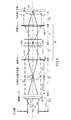
ここで、図を参照すると、図全体を通して同様の要素に同様に番号が付けられており、図3Aに示されるように、本発明によるHMDシステム100は、3つの主要なサブシステム、すなわちI)超小型InIユニット(マイクロInI)130と、II)リレー群120であって、内部に配置された、InIユニット130からライトフィールドを受け取るための可変焦点要素(VFE)122を有する、リレー群120と、III)リレー群120から調整された中間3D場面を受け取るための接眼レンズ光学部品110とを含む。図3Bに例示されるように、マイクロInIユニット130は、制約された視野ゾーンから見える3D場面の全方向視差ライトフィールドを再現することができ、全方向視差ライトフィールドは、水平視線方向と垂直視線方向との両方からの3D場面の視点の変化を提供する。制約された視野ゾーンは、光学的には、マイクロInIユニット130のアパーチャの制限に対応し、制約された視野ゾーンは、光学的には、表示システム100の射出瞳と共役であり、視聴者の眼は、再構築された3D場面を見るように置かれる。リレー群120はマイクロInIユニット130によって再構築された3D場面の中間像を生成し、その中央奥行き面(central depth plane:CDP)の位置は調整可能なようになっている。接眼レンズ110の倍率に応じて、CDPの位置は、光学的無限大(0ディオプトリ)〜20cm(5ディオプトリ)の近さまで広がる大きい奥行き範囲で3D場面の知覚を生成するために、約0.5mm〜数百ミリメートルの大きさまでの範囲で調整可能である。また、リレー群120は、再構築された3D場面AOBの凹面の反転を容易にすることもできる。接眼レンズ光学部品110は、視聴者の眼に調整可能な3Dライトフィールドをリイメージングし、3Dライトフィールドの調整可能な奥行き範囲を数メートルの遠さから数センチメートルの近さまで間隔がある幅広い奥行き体積空間に拡大する。ビームスプリッタ機能を有する光学部品であるシースルーユニット(図示せず)は、接眼レンズ光学部品110と光学的に連通して、シースルービューが望ましい場合に現世界場面を遮ることのない視野を光学的に可能にする。図3AのマイクロInIユニット130は、図3Bにさらに例示されるように、高解像度マイクロディスプレイおよびマイクロレンズアレイ(MLA)132を含む。MLA 132のレンズレット133の焦点距離は、fMLAとして示され、マイクロディスプレイ134とMLA 132との間の間隙は、gとして示される。2D要素画像(それぞれ3D場面AOBの異なる視点を表す)の組は、高解像度マイクロディスプレイ134上に表示することができる。MLA 132を通して、各要素画像は、空間的にインコヒーレントなオブジェクトとして機能し、要素画像の画素によって放射された円錐状の光線束は、交差して、光を放射して3D空間を占めるように見える3D場面の知覚を一体化して作り上げる。再構築されたミニチュアシーンの中央奥行き面(CDP)(z0の奥行き範囲)は、MLA 132から測定された距離lcdpに位置する。そのようなInIシステム130は、水平方向と垂直方向との両方における視差情報による3D表面形状AOBの再構築を可能にする。ユーザの観視のため、再構築された3D場面のライトフィールド(すなわち図3Bの曲線AOB)は、リレー群120を介して接眼レンズ光学部品110に光学的に結合することができる。分解能優先InIシステム(fMLA≠g)では、再構築された3D場面の中央奥行き面CDPは、マイクロディスプレイ134と光学的に共役であり、その位置は、
Referring now to the figures, like elements are similarly numbered throughout the figure, and as shown in FIG. 3A, the
![]()
![]()
![]()
![]()
図3A、4Aに示されるように、任意選択で、アパーチャアレイ136(MLA 132のピッチと整合する光線制御アパーチャのグループを含む)は、マイクロディスプレイ134とMLA 132との間に挿入することができる。各マイクロレンズ133に対応する小さいアパーチャは、望ましくない光線が隣接マイクロレンズ133に達することを阻止し、または近隣の要素画像からの光線がマイクロレンズ133に達することを阻止するとともに、意図された視野窓内の光線が光学部品を通して伝播し、アイボックスに達することを可能にする。例えば、アパーチャA1ブロックとアパーチャA2ブロックとの間の黒いゾーンは、ポイントP1からの破線の光線が、レンズレットMLA1に隣接するMLA2に達することを阻止する。阻止されたこれらの光線は、典型的には、InI表示システムにおいて観察される視野クロストークおよびゴースト像の主要な原因である。マイクロディスプレイ134からアパーチャアレイ136までの距離は、gaとして示され、アパーチャ開口部の直径は、paとして示され、
As shown in FIGS. 3A and 4A, an aperture array 136 (including a group of ray control apertures that match the pitch of the MLA 132) can optionally be inserted between the

固定アパーチャサイズを有するアパーチャアレイ136の使用における欠点の1つは、要素画像のサイズが変化した場合、各要素画像の端部の近くに位置する画素に対する光線を部分的に阻止する場合があることである。図4Aに例示されるように、レンズレットMLA1を通して伝播するはずのポイントP1からの光線のごく一部は、アパーチャA1とアパーチャA2との間の黒いゾーンによって阻止され、視聴者が各要素画像の端部の近くのポイントに対して画像明度の低減を観察するビネッティングのような効果を引き起こす。図4Bは、図4Aのものの代替の構成を示し、アパーチャアレイ136は、プログラマブル空間光変調器(spatial light modulator:SLM)135と交換され、その結果、各アパーチャのサイズおよび形状は、所望の光線の部分的阻止を回避するように動的に適応させることができる。図4Cは、本発明によるマイクロInIユニットの別の実施形態を示し、マイクロディスプレイ134およびアパーチャアレイ136は、制御自在な指向性放射を有する表示源131と交換され、発光方向は、各画素からの光線がそれらの対応するMLAレンズレット133のみに達するように精密に制御することができる。図4Dは、そのような表示源131の1つの可能な構成を実証し、空間光変調器135は、非指向性放射を有するバックライト源138と、非自発光型マイクロディスプレイ137との間に挿入されている。空間光変調器135は、マイクロディスプレイ137に照射され、MLA 132に達する光線の円錐角をプログラムおよび制御するように設定することができる。
One of the drawbacks of using the
従来のInIベースの表示システムは、典型的には、3D再構築ポイントの奥行きがCDPの奥行きからシフトしているときの空間分解能の急速な劣化による限られた被写界深度(DOF)に直面する。例えば、3D場面の体積は、視覚空間における空間分解能を3分(角度)またはより良好に維持するために、0.5ディオプトリ未満に制限する必要がある。図3Aの例示的な構成においてなど、高空間分解能を維持しながらはるかに大きい3D場面の体積をレンダリングするため、電子制御される可変焦点要素122が内側に挟まれたリレー群120は、マイクロInI 130と接眼レンズ110との間に挿入される。例示的なVFE 122は、液体レンズ、液晶レンズ、可変鏡、または他の任意の調整可能な光学技術(電気的に調整可能な光学技術など)を含む。異なる電圧をVFE 122に印加することによってリレー群120のオプティカルパワーφRを動的に制御することにより、リレー群120は、マイクロInI 130によって生成された再構築されたミニチュア3D場面の中間像A'O'B'を形成する。リレーされた中間場面の中央奥行き位置CDPは、接眼レンズ110に対して軸方向に(光軸に沿って)調整可能である。その結果、接眼レンズ110による拡大された3D仮想場面の奥行き体積は、高い横分解能および縦分解能を維持しながら、非常に近く(例えば、5ディオプトリ)から非常に遠く(例えば、0ディオプトリ)に軸方向にシフトすることができる。
Conventional InI-based display systems typically face a limited depth of field (DOF) due to the rapid degradation of spatial resolution when the depth of 3D reconstruction points is shifted from the depth of CDP. To do. For example, the volume of a 3D scene should be limited to less than 0.5 diopters in order to maintain spatial resolution in visual space of 3 minutes (angle) or better. To render a much larger volume of a 3D scene while maintaining high spatial resolution, such as in the exemplary configuration of FIG. 3A, a group of
図5は、図3Aのリレー群120などの可変焦点リレー群120の例示的な構成を概略的に例示し、マイクロInIユニット130に隣接する前部レンズ群「前部リレー」126と、システムストップとして機能する中間に位置するVFE光学部品122と、接眼レンズ110に隣接する後部レンズ群「後部リレー」124とを含む。リレー群120の複合パワーφRは、
FIG. 5 schematically illustrates an exemplary configuration of a variable
![]()
![]()
可変焦点リレーシステムの横倍率は、 The lateral magnification of the variable focus relay system is
φeは、接眼レンズ110のオプティカルパワーであり、ZRCDPは、リレーされたCDPから接眼レンズ110までの距離であると想定すると、接眼レンズ110を通した再構築された3D仮想場面の見かけのCDP位置は、
Assuming φ e is the optical power of the
接眼レンズ110を通した全システムの横倍率は、
The lateral magnification of the whole system through the
接眼レンズ110を通した全システムの視野(FOV)は、FOV=
uvfe=[(1−zxpφe)−(zxp+(1−zxpφe)t3)φ2]およびhvfe=[(1−zxpφe)−(zxp+(1−zxpφe)t3)φ2]−[(zxp+(1−zxpφe)t3)φ2+((1−zxpφe)−(zxp+(1−zxpφe)t3)φ2)]t2
をさらに定義する。
The field of view (FOV) of the entire system through the
u vfe = [(1-z xp φ e )-(z xp + (1-z xp φ e ) t 3 ) φ 2 ], and h vfe = [(1-z xp φ e )-(z xp + ( 1-z xp φ e) t 3) φ 2] - [(z xp + (1-z xp φ e) t 3)
Is further defined.
接眼レンズ110の射出瞳と光学的に共役であるようにVFE 122を設定すると((すなわちhvfe=0)、眼の入射瞳は、ディスプレイ134を見るように置かれ、hvfe=0を有し、FOVは、VFE 122のオプティカルパワーから独立している。式(9)の式は、
図5に例示されるように、可変焦点リレー群120の好ましい実施形態は、VFE 122が接眼レンズ110の射出瞳と光学的に共役となるようにするために((すなわちhvfe=0)、前部リレー群26の後側焦点距離にVFE 122を配置すること(すなわちt1=1/φ1)である。この好ましい実施形態を用いると、式(4)によって与えられるリレー群120の複合パワーφRは、
As illustrated in FIG. 5, the preferred embodiment of the variable
![]()
![]()
式(6)によって与えられる可変焦点リレーシステムの横倍率は、 The lateral magnification of the variable focus relay system given by equation (6) is
t1=1/φ1およびhvfe=0の場合、システムのFOVは、
式(10)〜(13)によって実証されるように、好ましい方法でのVFE 122の慎重な位置決めは、物体空間テレセントリシティのプロパティによる一定の主光線方向に起因して、リレー群120の複合オプティカルパワーがVFE 122のオプティカルパワーから独立して一定に維持されることを保証する。式(13)によってさらに実証されるように、接眼レンズ110を通したディスプレイの対する画角は、VFE 122のオプティカルパワーから独立して一定にさらに維持される。リレー群120に対して一定のオプティカルパワーを維持することは、CDPの焦点深度に関わらず、仮想的に再構築された3D場面が一定の視野を達成する上で役立つ。したがって、視線方向連動(gaze−contingent)または時間多重化モードにおけるシームまたはアーチファクトなしで、3D場面のはるかに大きい体積を仮想的に知覚することができる。注目すべき点は、t2=1/φ2が満たされる場合、式(12)によって与えられるリレー群120の横倍率を一定にさらに維持できることであり、それにより、可変焦点リレー群120は、ダブル・テレセントリック・システムになる。
As demonstrated by equations (10)-(13), the careful positioning of
図3Aの接眼レンズ110は、多くの異なる形態を取ることができる。例えば、光学式シースルーHMDのコンパクトな光学設計を達成するため、ウェッジ形状の自由曲面プリズムを取り入れることができ、ウェッジ形状の自由曲面プリズムを通して、マイクロInIユニット130およびリレー群120によって再構築された3D場面は、拡大されて見られる。ARシステムに対するシースルー能力を可能にするため、自由曲面プリズムによって現実世界場面に導入された視軸偏位および望ましくない収差を補正するように、表面の1つがビームスプリッタコーティングでコーティングされた自由曲面補正レンズを自由曲面プリズム接眼レンズに取り付けることができる。
The
本発明の別の観点では、リレー群120の一部は、調整可能な中間3D場面が自由曲面接眼レンズの内側に形成されるように、自由曲面接眼レンズなどの接眼レンズ光学部品110に組み込むことができる。それに関連して、接眼レンズは、例えば、ウェッジ形状の自由曲面導波路型プリズムである。図6Aは、複数の自由曲面光学表面によって形成された自由曲面導波路のようなプリズム850の概念を概略的に例示する。射出瞳は、拡大された3D場面を見るために使用の眼が置かれる場所に位置する。設計では、VFE 122に続く従来のリレー群220の一部は、プリズム850に組み込まれ、「VFEを有するリレー群」とラベル付けされたボックス内に含まれる自由曲面導波路型プリズム850の上部851によって機能が果たされる。3Dポイント(例えば、A)から放射された光線は、最初に、リレー群220の最も近い光学要素126で屈折し、プリズム850内に透過し、中間像(例えば、A')を生成するために1または複数の自由曲面での反射が続く。中間像(例えば、A')の軸位置は、VFE 122によって調整可能である。後続の表面による複数の連続的な反射および出口表面855を通した最終的な屈折により、光線は、システムの射出瞳に達することができる。異なる要素画像からの複数の光線束が存在するが、これらの光線束は、明らかに同じオブジェクトポイントから放射されたものであり、その束の各々は、オブジェクトの異なるビューを表し、射出瞳の異なる位置に入射する。これらの光線束は、眼の前に位置する仮想3Dポイント(例えば、「A」)を一体化して再構築する。複数の光学要素を必要とするよりむしろ、光学経路は、多面プリズム850内で自然に折り曲げられ、回転対称要素を使用した設計と比べて、光学部品の全体積および重量を実質的に低減する上で役立つ。従来のウェッジ形状の3面プリズムを使用した設計と比べて、導波路のような接眼レンズ設計は、リレー機能の一部を組み込み、スタンドアロンリレー群120を3面プリズムと組み合わせたものよりはるかにコンパクトなシステムを可能にする。コンパクト性の利点以外に、導波路のようなマルチフォールド接眼レンズ設計は、残りのリレー群およびマイクロInIユニットを水平方向においてこめかみ側の方に折り畳む能力を可能にするため、はるかに好ましいフォームファクタを提供する。マルチフォールドは、はるかに重量バランスの取れたシステムをもたらすのみならず、ウェッジ形状のプリズムを使用するよりも実質的に大きいシースルーFOVも可能にする。
In another aspect of the invention, a portion of
ARシステムに対するシースルー能力を可能にするため、接眼レンズ部分としてマーク付けされた図6Aのプリズム850の裏面の下部853は、ビーム分割鏡としてコーティングすることができ、少なくとも2つの自由曲面光学表面を含む自由曲面補正レンズ840は、自由曲面プリズム850によって現実世界場面に導入された視軸偏位および望ましくない収差を補正するようにプリズム850の裏面に取り付けることができる。シースルー概略レイアウトは、図6Bに示される。仮想ライトフィールドからの光線は、プリズム850の裏面で反射し、現実世界場面からの光線は、自由曲面補正レンズ840およびプリズム850を通して透過する。自由曲面補正レンズ840の前面は、プリズム850の裏面の形状と整合する。自由曲面補正レンズ840の後面は、レンズがプリズム850と組み合わされる際に現実世界場面から光線に導入されるシフトおよび歪みを最小化するように最適化することができる。追加の補正レンズ「補正要素(compensator)」は、全システムのフットプリントおよび重量を著しく増加することはない。
The
本発明の別の観点では、接眼レンズ部分としてマーク付けされた図6Aのプリズム850の裏面の下部853は、2つのセグメント、すなわちセグメント853−1およびセグメント853−2に分割することができる。図6Cに概略的に例示されるように、853−1のセグメントは、マイクロInIユニットによって生成されたライトフィールドを受け取る反射性または部分反射性の表面である。また、853−1のセグメント上のビーム分割鏡コーティングは、現実世界場面からの光線の透過も可能にする。セグメント853−2は、透過性または半透過性の表面であり、マイクロInIユニット130によって生成されたライトフィールドを受け取らず、現実世界場面からの光線のみを受け取る。図6Dは、プリズム850の裏面の正面図を概略的に例示する。2つの表面セグメント853−1および853−2は、マイクロInIユニット130によって再構築された3Dライトフィールドを受け取るために必要なアパーチャ窓の上方境界で交差し、2つの別個の自由曲面によって作ることができる。異なる光路を有する2つの別個のセグメント853−1、853−2への裏面853の下部の分割は、仮想ディスプレイ経路の制約を受け取ることなく、ディスプレイ経路のFOVを超えてシースルービューのFOVを実質的に拡大する能力を提供する。図6Cに示されるように、自由曲面補正レンズ840は、自由曲面プリズム850によって現実世界場面に導入された視軸偏位および望ましくない収差を補正するようにプリズム850の裏面に取り付けることができる。仮想ライトフィールドからの光線は、プリズム850の裏面のセグメント853−1で反射し、現実世界場面からの光線は、プリズム850のセグメント853−1および853−2と自由曲面補正レンズ840との両方を通して透過する。表面セグメント853−2は、自由曲面補正レンズ840と組み合わされる際にシースルービューの視覚的アーチファクトを最小化するように最適化することができる。自由曲面補正レンズ840の前面は、プリズム850の表面セグメント853−1および853−2の形状と整合する。自由曲面補正レンズ840の後面は、自由曲面補正レンズ840がプリズム850と組み合わされる際に現実世界場面から光線に導入されるシフトおよび歪みを最小化するように最適化することができる。
In another aspect of the invention, the
本発明のさらなる別の観点によれば、図7Aは、図6Aの概念システムを具体化する物理システムの光学設計を概略的に例示する。図7Aは、ライトフィールドディスプレイ経路の2D光学レイアウトを例示し、図7Bは、シースルー経路の光学レイアウトを示す。ライトフィールドディスプレイの光学システムは、マイクロInIユニット、VFEを有するリレー群、および自由曲面導波路を含む。リレー群の一部は、導波路に組み込むことができる。マイクロInIユニットは、マイクロディスプレイS0、ピンホールアレイS1、およびマイクロレンズアレイS2を含む。リレー群は、4つのレンズと、市販のVFE(Optotune Inc.によるElectrical Lens EL10−30)と、2つの自由曲面(表面S19およびS20)とを含む。自由曲面導波路型プリズム900は、S19、S20、S21、およびS22としてそれぞれラベル付けされた複数の自由曲面光学表面によって形成することができる。本設計では、VFEに続く従来のリレー群の一部は、プリズム900に組み込むことができ、表面S19およびS20によって機能を果たすことができる。3Dポイント(例えば、A)から放射された光線は、最初に、プリズム900の表面S19で屈折し、中間像(例えば、A')を生成するために表面S20での反射が続く。中間像(例えば、A')の軸位置は、VFEによって調整可能である。表面S21'およびS22−1でのもう2つの連続的な反射並びに表面S21を通した最終的な屈折により、光線は、システムの射出瞳に達することができる。異なる要素画像からの複数の光線束が存在するが、これらの光線束は、明らかに同じオブジェクトポイントから放射され、その各々は、オブジェクトの異なるビューを表し、射出瞳の異なる位置に入射する。これらの光線束は、眼の前に位置する仮想3Dポイントを一体化して再構築する。導波路の表面S21'で反射した光線は、全内部反射の条件を満たす必要がある。プリズム900の裏面S22−1、S22−2は、現実世界場面のビューを阻止する没入型HMDシステムを構築するために、ミラーコーティングでコーティングすることができる。或いは、表面S22−1は、図7Bに示されるように、補助レンズを使用した光学式シースルー能力が望ましい場合、ビームスプリッタコーティングでコーティングすることができる。
According to yet another aspect of the invention, FIG. 7A schematically illustrates an optical design of a physical system embodying the conceptual system of FIG. 6A. FIG. 7A illustrates a 2D optical layout of a light field display path, and FIG. 7B shows an optical layout of a see-through path. The optical system of a light field display includes a micro InI unit, a group of relays with VFE, and a freeform waveguide. A part of the relay group can be incorporated in the waveguide. The micro InI unit includes a micro display S0, a pinhole array S1, and a microlens array S2. The relay group includes four lenses, a commercially available VFE (Electrical Lens EL10-30 by Optotune Inc.) and two free-form surfaces (surfaces S19 and S20). The free-
本明細書で開示される設計では、Z軸は、視線方向に沿い、Y軸は、左右の瞳孔を結ぶ方向と位置合わせされた水平方向に平行であり、およびX軸は、頭の向きと位置合わせされた垂直方向にあることに留意すべきである。その結果、全導波路システムは、水平(YOZ)平面に対して対称であり、光学表面(S19、S20、S21、およびS22)は、水平なY軸に沿って非共軸であり、且つ垂直なX軸を中心として回転する。光学経路は、水平なYOZ平面において折り曲げられる。この配置により、マイクロInIユニットおよび可変焦点リレー群は、ユーザの頭のこめかみ側に装着することができ、バランスの取れた人間工学的なシステムパッケージングを提供することができる。 In the designs disclosed herein, the Z axis is along the line-of-sight direction, the Y axis is parallel to the horizontal direction aligned with the direction connecting the left and right pupils, and the X axis is the head orientation. Note that it is vertically aligned. As a result, the entire waveguide system is symmetric with respect to the horizontal (YOZ) plane, and the optical surfaces (S19, S20, S21, and S22) are non-coaxial along the horizontal Y-axis and vertical. Rotate around the X axis. The optical path is folded in the horizontal YOZ plane. With this arrangement, the micro InI unit and variable focus relay group can be mounted on the temple side of the user's head, providing a balanced and ergonomic system packaging.
表1は、図7Aのシステムの重要な性能仕様のいくつかを強調する。システムは、3D場面の真の3Dライトフィールドをレンダリングする能力を提供し、35°の対角線のFOVに対しており、視覚空間において1つの画素あたり2分(角度)の高さの光分解能を達成する。その上、システムは、単眼ディスプレイに対して約0.1ディオプトリの高い縦分解能を有し、0〜5ディオプトリで調整可能な大きい奥行き範囲を提供する。その上、システムは、約0.5/mm2の高いビュー密度(view density)を達成し、ビュー密度σは、射出瞳の単位面積あたりの一意のビューの数として定義され、
表2〜5では、光学表面データの形態で図7Aのシステムの例示的な実装形態が提供される。表2は、ディスプレイ経路の基本的なパラメータを要約する(単位:mm)。表3〜5は、非球面の光学表面を定義する最適化係数を提供する。 Tables 2-5 provide exemplary implementations of the system of FIG. 7A in the form of optical surface data. Table 2 summarizes the basic parameters of the display path (unit: mm). Tables 3-5 provide optimization factors that define aspherical optical surfaces.
6μmの小ささの画素を有する高解像度マイクロディスプレイは、高解像度の仮想再構築3D画像を達成するために取り入れられる。マイクロInIユニットに対するそのような高解像度画像を達成するため、具体的には、非球面によって形成されたマイクロレンズアレイ(MLA)を設計することができる。MLAの非球面の各々は、 A high resolution microdisplay with pixels as small as 6 μm is incorporated to achieve high resolution virtual reconstructed 3D images. In order to achieve such high resolution images for micro InI units, specifically microlens arrays (MLA) formed by aspheric surfaces can be designed. Each of the aspherical surfaces of MLA is
シースルーFOVの拡大を可能にするため、自由曲面導波路型プリズム900は、表面S19、S20、S21/S21'、S22−1、S22−2とそれぞれラベル付けされた5つの自由曲面によって形成することができる。自由曲面補正レンズは、2つの自由曲面によって形成することができ、前面は、導波路プリズム900の表面S22−1およびS22−2と同じ表面仕様を共有し、裏面は、表面S23と示される。S22−1の表面セグメントは、マイクロInIユニットによって生成されたライトフィールドを受け取る反射性または部分反射性の表面である。また、S22−1のセグメント上のビーム分割鏡コーティングは、シースルー能力に対する現実世界場面からの光線の透過も可能にする。表面セグメントS22−2は、透過性または半透過性の表面であり、マイクロInIユニットによって生成されたライトフィールドを受け取らず、現実世界場面からの光線のみを受け取る。
In order to allow expansion of the see-through FOV, the free-form surface
S19、S20、S21/S21'、S22−1、S23を含む自由曲面は、 The free-form surface including S19, S20, S21 / S21 ′, S22-1 and S23 is
設計プロセス中、表面セグメントS22−1に対する仕様は、マイクロInIユニット、リレーレンズ群、および表面S19、S20、S21/21'、S22−1から構成されるプリズム900を通したライトフィールドディスプレイ経路の最適化後に得られた。最初に、ライトフィールドディスプレイ経路に対して、表面S20およびS22−1の必要なアパーチャ寸法が決定された。次いで、表面S22−2が作成されたSolidworks(登録商標)などの3Dモデリングソフトウェアに表面S20、S21、S22−1がインポートされた。表面S22−2の形状は、次の要件、すなわち(1)ディスプレイ経路によって定義された表面S22−1に必要なアパーチャの上方境界線に沿ってまたは上方境界線の上方で表面S22−1と交差すること、(2)表面S22−2と表面S22−2との間の交差線に沿って、表面S22−2上の交点における表面傾斜がほぼ整合することであるが、等しくない場合、表面S22−1上のそれらの対応する点が、2つの表面がほぼ連続しているように見えることを保証し、それにより、整合する自由曲面補正レンズと組み合わされた際にシースルービューに対する視覚的アーチファクトが最小化されること、(3)表面S22−2が、ディスプレイ経路によって定義された表面S20に必要なアパーチャの下方境界線に沿ってまたは下方境界線の下方で表面S20と交差すること、(4)表面S21およびS22−2間の全体的な厚さが最小化されることを満たすことにより、モデリングソフトウェアにおいて作成された。最後に、閉鎖性の自由曲面導波路型プリズムを作成するため、表面S22−2の自由曲面形状は、表面S19、S20、S21/21'、S22−1と組み合わされた3Dモデリングソフトウェアにおいて得られる。図7Bは、上記で説明される方法を通して、実質的に拡大されたシースルーFOVを実証した。
During the design process, the specifications for the surface segment S22-1 are optimized for the light field display path through the micro InI unit, the relay lens group, and the
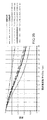
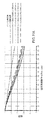
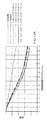
設計プロセス中、3つの代表波長465nm、550nm、630nmが選択され、それらの波長は、選択されたOLEDマイクロディスプレイ内の青色、緑色および赤色エミッタのピーク発光スペクトルに対応する。MLAの合計で21個のレンズレットがサンプリングされ、各々は、9つの要素画像ポイントを表し、合計で189のフィールドサンプルになる。画質を評価するため、接眼レンズと同じ倍率を有する理想的なレンズがシステムの射出瞳(視野窓)に配置され、それにより最終的な画像に対して20.83lp/mmのカットオフ周波数が生じる(マイクロディスプレイの画素サイズによって制限される)。設計されたシステムの光学性能は、3つの設計波長に対する代表画角で評価された。調整可能なレンズVFEの倍率を変更することにより、光学性能の著しい変性をもたらすことなく、中央奥行き面を大きい範囲(例えば、0〜3ディオプトリ)で軸方向にシフトすることができる。図8〜10は、3、1、および0ディオプトリの深度でそれぞれ設定されたCDP上で再構築されたポイントに対する多色変調伝達関数(MTF)をプロットする。各CDP位置に対し、2組のMTFがプロットされ、1つは、軸上MLAに対応するフィールドに対するものであり、1つは、端部の近くの最も遠いMLAに対応するフィールドに対するものである。 During the design process, three representative wavelengths 465 nm, 550 nm, 630 nm were selected, which wavelengths correspond to the peak emission spectra of the blue, green and red emitters in the selected OLED microdisplay. A total of 21 lenslets are sampled in the MLA, each representing 9 elemental image points, for a total of 189 field samples. To evaluate the image quality, an ideal lens with the same magnification as the eyepiece is placed in the exit pupil (field window) of the system, which results in a cut-off frequency of 20.83 lp / mm for the final image. (Limited by the pixel size of the microdisplay). The optical performance of the designed system was evaluated at representative angles of view for the three design wavelengths. By changing the magnification of the adjustable lens VFE, the central depth plane can be axially shifted over a large range (eg, 0-3 diopters) without significantly modifying the optical performance. 8-10 plot the polychromatic modulation transfer function (MTF) for the reconstructed points on the CDP set at depths of 3, 1, and 0 diopters, respectively. Two sets of MTFs are plotted for each CDP position, one for the field corresponding to the on-axis MLA and one for the field corresponding to the furthest MLA near the edge. ..
他方では、特定の調整可能な状態に対して再構築画像が中央奥行き面からシフトされる際に3D再構築ポイントの画質がどのように劣化するかを評価することが等しく重要である。これは、調整可能なレンズの倍率を変更することなく、中央奥行き面をわずかな距離だけシフトすることによって評価することができる。図11〜14は、CDPから0.25、0.5、0.75、および1ディオプトリだけそれぞれシフトされた再構築ポイントに対する多色MTFをプロットする。各深度に対し、2組のMTFがプロットされ、1つは、軸上MLAに対応するフィールドに対するものであり、1つは、端部の近くの最も遠いMLAに対応するフィールドに対するものである。 On the other hand, it is equally important to evaluate how the quality of the 3D reconstructed points degrades when the reconstructed image is shifted from the central depth plane for a particular adjustable state. This can be evaluated by shifting the central depth plane by a small distance without changing the magnification of the adjustable lens. 11-14 plot the polychromatic MTF for reconstruction points shifted by 0.25, 0.5, 0.75, and 1 diopter respectively from the CDP. For each depth, two sets of MTFs are plotted, one for the field corresponding to the on-axis MLA and one for the farthest MLA near the edge.
図15は、65°×40°のFOVに対する多色MTFをプロットする。FOV全体にわたり、シースルー経路は、30サイクル/度の周波数で50%を超える平均MTF値を達成し(20/20の正常視力に対応する)、60サイクル/度の周波数でほぼ20%の平均MTF値を達成した(20/10の視力または0.5分(角度)の視力に対応する)。 FIG. 15 plots the polychromatic MTF for a 65 ° × 40 ° FOV. Throughout the FOV, the see-through path achieved an average MTF value of over 50% at a frequency of 30 cycles / degree (corresponding to normal vision of 20/20) and an average MTF of almost 20% at a frequency of 60 cycles / degree. Values were achieved (corresponding to 20/10 visual acuity or 0.5 min (angle) visual acuity).
Claims (27)
光を受け取り、且つ光を前記プリズムの本体部内に屈折させるように配置された第1の自由曲面光学表面と、
前記第1の自由曲面光学表面から前記屈折された光を受け取り、前記プリズムの前記本体部内に前記受け取った光を反射させて前記本体部内に中間像を提供するように配置された第2の自由曲面光学表面と、
複合自由曲面光学表面であって、
前記第2の自由曲面光学表面に結合された上部自由曲面光学表面であって、前記第1の自由曲面光学表面からの光がその表面に入射しないように配置されているものである、前記上部自由曲面光学表面と、
前記上部自由曲面光学表面に結合された下部自由曲面光学表面であって、前記上部自由曲面光学表面は、前記下部自由曲面光学表面と前記第2の自由曲面光学表面との間に配置されているものである、前記下部自由曲面光学表面と
を有する前記複合自由曲面光学表面と
を有する自由曲面導波路型プリズム。 A free-form surface-waveguide prism,
A first free-form optical surface arranged to receive light and refract the light into the body of the prism;
A second freedom arranged to receive the refracted light from the first free-form curved optical surface and reflect the received light into the body of the prism to provide an intermediate image in the body. A curved optical surface,
A compound free-form optical surface,
An upper free-form curved optical surface coupled to the second free-form curved optical surface, the upper free-form curved optical surface being arranged so that light from the first free-form curved optical surface does not enter the surface. A free-form optical surface,
A lower freeform optical surface coupled to the upper freeform optical surface, the upper freeform optical surface being disposed between the lower freeform optical surface and the second freeform optical surface. And a composite free-form optical surface having the lower free-form optical surface.
当該システムの光軸に沿った選択された位置において、選択された3D場面のライトフィールドを生成するように構成された超小型InIユニット(マイクロInI)と、
リレーユニットであって、その内部に配置された可変焦点要素(VFE)を有し、前記光軸上において前記選択された位置が光学的に共役となる位置に配置され、前記超小型InIユニットによって生成された前記ライトフィールドを受け取るように構成されているものである、前記リレーユニットと、
前記リレーユニットから光を受け取るための請求項1〜13のいずれか1つに記載の自由曲面導波路型プリズムであって、前記システムの射出瞳において前記ヘッドマウント・ディスプレイ・システムのユーザによって観視される前記3D場面の像を提供するものである、前記自由曲面導波路型プリズムと
を有し、
前記可変焦点要素(VFE)は、前記プリズムの前記本体部内の前記中間像の位置を調整するように構成されているものである、
ヘッドマウント・ディスプレイ・インテグラル・イメージング(InI)システム。 A head mounted display integral imaging (InI) system,
A microminiature InI unit (micro InI) configured to generate a light field of a selected 3D scene at a selected position along the optical axis of the system;
A relay unit having a variable focus element (VFE) arranged therein, arranged at a position on the optical axis where the selected position is optically conjugate, and The relay unit being configured to receive the generated light field,
A free-form surface-waveguide prism according to any one of claims 1 to 13 for receiving light from the relay unit, as viewed by a user of the head-mounted display system at an exit pupil of the system. And a free-form waveguide-type prism for providing an image of the 3D scene
The variable focus element (VFE) is configured to adjust the position of the intermediate image within the body of the prism,
Head-mounted display integral imaging (InI) system.
Priority Applications (1)
| Application Number | Priority Date | Filing Date | Title |
|---|---|---|---|
| JP2023170988A JP2024001099A (en) | 2017-03-09 | 2023-09-30 | Free-form prism and head-mounted display with increased field of view |
Applications Claiming Priority (3)
| Application Number | Priority Date | Filing Date | Title |
|---|---|---|---|
| US201762469104P | 2017-03-09 | 2017-03-09 | |
| US62/469,104 | 2017-03-09 | ||
| PCT/US2018/021098 WO2018165123A1 (en) | 2017-03-09 | 2018-03-06 | Freeform prism and head-mounted display with increased field of view |
Related Child Applications (1)
| Application Number | Title | Priority Date | Filing Date |
|---|---|---|---|
| JP2023170988A Division JP2024001099A (en) | 2017-03-09 | 2023-09-30 | Free-form prism and head-mounted display with increased field of view |
Publications (2)
| Publication Number | Publication Date |
|---|---|
| JP2020514810A true JP2020514810A (en) | 2020-05-21 |
| JP2020514810A5 JP2020514810A5 (en) | 2021-04-15 |
Family
ID=63447895
Family Applications (2)
| Application Number | Title | Priority Date | Filing Date |
|---|---|---|---|
| JP2019548958A Pending JP2020514810A (en) | 2017-03-09 | 2018-03-06 | Free-form surface prism and head-mounted display with magnified field of view |
| JP2023170988A Pending JP2024001099A (en) | 2017-03-09 | 2023-09-30 | Free-form prism and head-mounted display with increased field of view |
Family Applications After (1)
| Application Number | Title | Priority Date | Filing Date |
|---|---|---|---|
| JP2023170988A Pending JP2024001099A (en) | 2017-03-09 | 2023-09-30 | Free-form prism and head-mounted display with increased field of view |
Country Status (9)
| Country | Link |
|---|---|
| US (1) | US20200386993A1 (en) |
| EP (1) | EP3593200A4 (en) |
| JP (2) | JP2020514810A (en) |
| KR (1) | KR20190131510A (en) |
| CN (1) | CN110914741A (en) |
| AU (1) | AU2018231087A1 (en) |
| CA (1) | CA3055374A1 (en) |
| IL (1) | IL269044A (en) |
| WO (1) | WO2018165123A1 (en) |
Cited By (2)
| Publication number | Priority date | Publication date | Assignee | Title |
|---|---|---|---|---|
| WO2021246634A1 (en) * | 2020-06-02 | 2021-12-09 | 주식회사 피앤씨솔루션 | Augmented reality optical system comprising reflective surface, and head-mounted display device using same |
| US11947134B2 (en) | 2021-01-22 | 2024-04-02 | National Taiwan University | Device of generating 3D light-field image |
Families Citing this family (5)
| Publication number | Priority date | Publication date | Assignee | Title |
|---|---|---|---|---|
| GB2468997A (en) | 2008-01-22 | 2010-09-29 | Univ Arizona State | Head-mounted projection display using reflective microdisplays |
| GB201800173D0 (en) * | 2018-01-05 | 2018-02-21 | Yoentem Ali Oezguer | Multi-angle light capture display system |
| KR102597609B1 (en) * | 2018-11-09 | 2023-11-02 | 스냅 인코포레이티드 | Projection lens with four spherical glass elements |
| CN112882248B (en) * | 2021-01-15 | 2022-05-17 | 驻景(广州)科技有限公司 | Display module assembly of light beam divergence angle deflection aperture secondary restraint |
| CN113568141B (en) * | 2021-07-16 | 2022-10-21 | Oppo广东移动通信有限公司 | Lens, projection optical machine and near-to-eye display equipment |
Citations (3)
| Publication number | Priority date | Publication date | Assignee | Title |
|---|---|---|---|---|
| JP2002049001A (en) * | 2000-08-01 | 2002-02-15 | Olympus Optical Co Ltd | Image display device |
| WO2015134740A1 (en) * | 2014-03-05 | 2015-09-11 | Arizona Board Of Regents On Behalf Of The University Of Arizona | Wearable 3d augmented reality display with variable focus and/or object recognition |
| WO2015184409A1 (en) * | 2014-05-30 | 2015-12-03 | Magic Leap, Inc. | Methods and systems for displaying stereoscopy with a freeform optical system with addressable focus for virtual and augmented reality |
Family Cites Families (13)
| Publication number | Priority date | Publication date | Assignee | Title |
|---|---|---|---|---|
| JP4035476B2 (en) * | 2003-04-23 | 2008-01-23 | キヤノン株式会社 | Scanning optical system, scanning image display apparatus, and image display system |
| WO2010123934A1 (en) * | 2009-04-20 | 2010-10-28 | The Arizona Board Of Regents On Behalf Of The University Of Arizona | Optical see-through free-form head-mounted display |
| DE102010040030B4 (en) * | 2010-08-31 | 2017-02-02 | Fraunhofer-Gesellschaft zur Förderung der angewandten Forschung e.V. | Lens and imaging system |
| JP5603716B2 (en) * | 2010-09-06 | 2014-10-08 | オリンパス株式会社 | PRISM OPTICAL SYSTEM, IMAGE DISPLAY DEVICE AND IMAGING DEVICE USING PRISM OPTICAL SYSTEM |
| US10156722B2 (en) * | 2010-12-24 | 2018-12-18 | Magic Leap, Inc. | Methods and systems for displaying stereoscopy with a freeform optical system with addressable focus for virtual and augmented reality |
| EP2656135B1 (en) * | 2010-12-24 | 2022-05-04 | Magic Leap, Inc. | Freeform waveguide prism |
| JP6141584B2 (en) * | 2012-01-24 | 2017-06-07 | アリゾナ ボード オブ リージェンツ オン ビハーフ オブ ザ ユニバーシティ オブ アリゾナ | Compact line-of-sight head-mounted display |
| JP6111635B2 (en) * | 2012-02-24 | 2017-04-12 | セイコーエプソン株式会社 | Virtual image display device |
| CN104813218A (en) * | 2012-09-11 | 2015-07-29 | 奇跃公司 | Ergonomic head mounted display device and optical system |
| IN2015DN02476A (en) * | 2012-10-18 | 2015-09-11 | Univ Arizona State | |
| JP6221223B2 (en) * | 2012-11-16 | 2017-11-01 | セイコーエプソン株式会社 | Optical member and virtual image display device |
| US9857591B2 (en) * | 2014-05-30 | 2018-01-02 | Magic Leap, Inc. | Methods and system for creating focal planes in virtual and augmented reality |
| JP6264878B2 (en) * | 2013-12-24 | 2018-01-24 | セイコーエプソン株式会社 | Light guide device, virtual image display device, and light guide device manufacturing method |
-
2018
- 2018-03-06 AU AU2018231087A patent/AU2018231087A1/en not_active Abandoned
- 2018-03-06 JP JP2019548958A patent/JP2020514810A/en active Pending
- 2018-03-06 US US16/491,842 patent/US20200386993A1/en active Pending
- 2018-03-06 EP EP18764738.3A patent/EP3593200A4/en active Pending
- 2018-03-06 WO PCT/US2018/021098 patent/WO2018165123A1/en unknown
- 2018-03-06 CA CA3055374A patent/CA3055374A1/en active Pending
- 2018-03-06 KR KR1020197029321A patent/KR20190131510A/en not_active Application Discontinuation
- 2018-03-06 CN CN201880030598.5A patent/CN110914741A/en active Pending
-
2019
- 2019-09-01 IL IL26904419A patent/IL269044A/en unknown
-
2023
- 2023-09-30 JP JP2023170988A patent/JP2024001099A/en active Pending
Patent Citations (3)
| Publication number | Priority date | Publication date | Assignee | Title |
|---|---|---|---|---|
| JP2002049001A (en) * | 2000-08-01 | 2002-02-15 | Olympus Optical Co Ltd | Image display device |
| WO2015134740A1 (en) * | 2014-03-05 | 2015-09-11 | Arizona Board Of Regents On Behalf Of The University Of Arizona | Wearable 3d augmented reality display with variable focus and/or object recognition |
| WO2015184409A1 (en) * | 2014-05-30 | 2015-12-03 | Magic Leap, Inc. | Methods and systems for displaying stereoscopy with a freeform optical system with addressable focus for virtual and augmented reality |
Cited By (4)
| Publication number | Priority date | Publication date | Assignee | Title |
|---|---|---|---|---|
| WO2021246634A1 (en) * | 2020-06-02 | 2021-12-09 | 주식회사 피앤씨솔루션 | Augmented reality optical system comprising reflective surface, and head-mounted display device using same |
| KR20210149321A (en) * | 2020-06-02 | 2021-12-09 | 주식회사 피앤씨솔루션 | Optical system for augmented reality with a reflective surface and a head mounted display apparatus using thereof |
| KR102498191B1 (en) * | 2020-06-02 | 2023-02-10 | 주식회사 피앤씨솔루션 | Optical system for augmented reality with a reflective surface and a head mounted display apparatus using thereof |
| US11947134B2 (en) | 2021-01-22 | 2024-04-02 | National Taiwan University | Device of generating 3D light-field image |
Also Published As
| Publication number | Publication date |
|---|---|
| KR20190131510A (en) | 2019-11-26 |
| US20200386993A1 (en) | 2020-12-10 |
| CA3055374A1 (en) | 2018-09-13 |
| JP2024001099A (en) | 2024-01-09 |
| AU2018231087A1 (en) | 2019-09-26 |
| EP3593200A4 (en) | 2020-12-23 |
| IL269044A (en) | 2019-10-31 |
| WO2018165123A1 (en) | 2018-09-13 |
| EP3593200A1 (en) | 2020-01-15 |
| CN110914741A (en) | 2020-03-24 |
Similar Documents
| Publication | Publication Date | Title |
|---|---|---|
| JP7185331B2 (en) | How to render light field images for integral imaging light field displays | |
| JP7185303B2 (en) | Head-mounted Lightfield Display with Integral Imaging and Relay Optics | |
| JP7182796B2 (en) | Head-mounted Lightfield Display Using Integral Imaging and Waveguide Prisms | |
| JP7213002B2 (en) | Stereoscopic display with addressable focal cues | |
| JP2024001099A (en) | Free-form prism and head-mounted display with increased field of view | |
| KR20160135744A (en) | Wearable 3d augmented reality display | |
| Zhang et al. | Design and implementation of an optical see-through near-eye display combining Maxwellian-view and light-field methods |
Legal Events
| Date | Code | Title | Description |
|---|---|---|---|
| A521 | Request for written amendment filed |
Free format text: JAPANESE INTERMEDIATE CODE: A523 Effective date: 20210305 |
|
| A621 | Written request for application examination |
Free format text: JAPANESE INTERMEDIATE CODE: A621 Effective date: 20210305 |
|
| A977 | Report on retrieval |
Free format text: JAPANESE INTERMEDIATE CODE: A971007 Effective date: 20211228 |
|
| A131 | Notification of reasons for refusal |
Free format text: JAPANESE INTERMEDIATE CODE: A131 Effective date: 20220125 |
|
| A521 | Request for written amendment filed |
Free format text: JAPANESE INTERMEDIATE CODE: A523 Effective date: 20220424 |
|
| A131 | Notification of reasons for refusal |
Free format text: JAPANESE INTERMEDIATE CODE: A131 Effective date: 20220823 |
|
| A601 | Written request for extension of time |
Free format text: JAPANESE INTERMEDIATE CODE: A601 Effective date: 20221119 |
|
| A521 | Request for written amendment filed |
Free format text: JAPANESE INTERMEDIATE CODE: A523 Effective date: 20230222 |
|
| A02 | Decision of refusal |
Free format text: JAPANESE INTERMEDIATE CODE: A02 Effective date: 20230530 |
|
| A521 | Request for written amendment filed |
Free format text: JAPANESE INTERMEDIATE CODE: A523 Effective date: 20230930 |
|
| A911 | Transfer to examiner for re-examination before appeal (zenchi) |
Free format text: JAPANESE INTERMEDIATE CODE: A911 Effective date: 20231121 |
|
| A912 | Re-examination (zenchi) completed and case transferred to appeal board |
Free format text: JAPANESE INTERMEDIATE CODE: A912 Effective date: 20240112 |