JP2020141294A - Signal processing method, signal processing device, and communication system - Google Patents
Signal processing method, signal processing device, and communication system Download PDFInfo
- Publication number
- JP2020141294A JP2020141294A JP2019036315A JP2019036315A JP2020141294A JP 2020141294 A JP2020141294 A JP 2020141294A JP 2019036315 A JP2019036315 A JP 2019036315A JP 2019036315 A JP2019036315 A JP 2019036315A JP 2020141294 A JP2020141294 A JP 2020141294A
- Authority
- JP
- Japan
- Prior art keywords
- polarization
- signal
- component
- impulse response
- imaginary
- Prior art date
- Legal status (The legal status is an assumption and is not a legal conclusion. Google has not performed a legal analysis and makes no representation as to the accuracy of the status listed.)
- Granted
Links
Images


Classifications
-
- H—ELECTRICITY
- H04—ELECTRIC COMMUNICATION TECHNIQUE
- H04L—TRANSMISSION OF DIGITAL INFORMATION, e.g. TELEGRAPHIC COMMUNICATION
- H04L27/00—Modulated-carrier systems
- H04L27/01—Equalisers
-
- H—ELECTRICITY
- H04—ELECTRIC COMMUNICATION TECHNIQUE
- H04B—TRANSMISSION
- H04B10/00—Transmission systems employing electromagnetic waves other than radio-waves, e.g. infrared, visible or ultraviolet light, or employing corpuscular radiation, e.g. quantum communication
- H04B10/25—Arrangements specific to fibre transmission
- H04B10/2507—Arrangements specific to fibre transmission for the reduction or elimination of distortion or dispersion
-
- H—ELECTRICITY
- H04—ELECTRIC COMMUNICATION TECHNIQUE
- H04B—TRANSMISSION
- H04B10/00—Transmission systems employing electromagnetic waves other than radio-waves, e.g. infrared, visible or ultraviolet light, or employing corpuscular radiation, e.g. quantum communication
- H04B10/60—Receivers
- H04B10/61—Coherent receivers
- H04B10/616—Details of the electronic signal processing in coherent optical receivers
- H04B10/6161—Compensation of chromatic dispersion
-
- H—ELECTRICITY
- H04—ELECTRIC COMMUNICATION TECHNIQUE
- H04J—MULTIPLEX COMMUNICATION
- H04J11/00—Orthogonal multiplex systems, e.g. using WALSH codes
-
- H—ELECTRICITY
- H04—ELECTRIC COMMUNICATION TECHNIQUE
- H04J—MULTIPLEX COMMUNICATION
- H04J14/00—Optical multiplex systems
- H04J14/06—Polarisation multiplex systems
-
- H—ELECTRICITY
- H04—ELECTRIC COMMUNICATION TECHNIQUE
- H04L—TRANSMISSION OF DIGITAL INFORMATION, e.g. TELEGRAPHIC COMMUNICATION
- H04L27/00—Modulated-carrier systems
- H04L27/32—Carrier systems characterised by combinations of two or more of the types covered by groups H04L27/02, H04L27/10, H04L27/18 or H04L27/26
- H04L27/34—Amplitude- and phase-modulated carrier systems, e.g. quadrature-amplitude modulated carrier systems
- H04L27/38—Demodulator circuits; Receiver circuits
Landscapes
- Engineering & Computer Science (AREA)
- Computer Networks & Wireless Communication (AREA)
- Signal Processing (AREA)
- Physics & Mathematics (AREA)
- Electromagnetism (AREA)
- Optical Communication System (AREA)
Abstract
Description
本発明は、信号処理方法、信号処理装置及び通信システムに関する。 The present invention relates to signal processing methods, signal processing devices and communication systems.
高次多値の高速ボーレート信号は、反射、レーン間スキュー、IQインバランス等にセンシティブであるため、送受信器で精密なキャリブレーションが求められる。従来の技術では、受信された既知信号から送信機および受信機の伝達関数を推定し、送信機の予等化回路及び受信機の等化回路により信号歪みを精度よく補償する(例えば、特許文献1参照)。この技術は、静的な波形歪み要因に対しては非常に有効であり、高次多値信号の送受信においては必須の技術である。 High-order multi-valued high-speed baud rate signals are sensitive to reflection, inter-lane skew, IQ imbalance, etc., so precise calibration is required at the transmitter / receiver. In the conventional technique, the transfer function of the transmitter and the receiver is estimated from the received known signal, and the signal distortion is accurately compensated by the equalization circuit of the transmitter and the equalization circuit of the receiver (for example, Patent Document). 1). This technique is very effective against static waveform distortion factors, and is an indispensable technique for transmitting and receiving high-order multi-valued signals.
しかしながら、各種デバイスの経時変化や変調器バイアス等の時間変動する波形歪み要因に対しては、適応等化器を多段構成にするなどして補償する必要があった。例えば、従来の等化器構成(例えば、非特許文献文献1参照)では、受信した複素信号を実部・虚部に分けて、各々に波長分散補償を複素信号処理で行う。このような処理により、波長分散による信号歪みがあり、かつIQミキシングの存在下においても、受信機のIQインバランスやスキューを動的に補償可能である。しかしながら、この等化器構成では、送信機におけるIQインバランスおよびスキューを補償することが出来ない。よって、受信機は、復調処理を行った後に、各偏波成分に実数信号処理による2x2MIMO(Multiple Input Multiple Output)信号処理(例えば、非特許文献2のFig.2におけるGainIQ+Skew Controlの部分)を行うことが必要となる。 However, it is necessary to compensate for the time-varying waveform distortion factors such as the time-dependent changes of various devices and the modulator bias by making the adaptive equalizer a multi-stage configuration. For example, in the conventional equalizer configuration (see, for example, Non-Patent Document 1), the received complex signal is divided into a real part and an imaginary part, and wavelength dispersion compensation is performed for each part by complex signal processing. By such processing, there is signal distortion due to wavelength dispersion, and IQ imbalance and skew of the receiver can be dynamically compensated even in the presence of IQ mixing. However, this equalizer configuration cannot compensate for IQ imbalance and skew in the transmitter. Therefore, after performing demodulation processing, the receiver performs 2x2 MIMO (Multiple Input Multiple Output) signal processing by real number signal processing for each polarization component (for example, Gain IQ + Skew Control part in Fig. 2 of Non-Patent Document 2). It is necessary to do.
しかしながら、非特許文献2の技術では、受信機の適応等化器が多段構成になる。この構成の初段では、等化器を含んだ復調信号処理を行う。受信機は、初段の復調信号処理が収束したのちに、後段に配置された送信器内信号歪み補償用のMIMO等化器を動作させる。そのため、復調処理全体の適応動作が複雑化し、適応信号処理の収束が遅くなるという課題があった。更に、送信機における歪み成分が大きいと、2つの等化器の適応等化が振動もしくは発散することがあった。
However, in the technique of Non-Patent
上記事情に鑑み、本発明は、精度よく歪み補償を行う等化処理の処理速度を速めることができる信号処理方法、信号処理装置及び通信システムを提供することを目的としている。 In view of the above circumstances, an object of the present invention is to provide a signal processing method, a signal processing device, and a communication system capable of increasing the processing speed of the equalization processing that accurately compensates for distortion.
本発明の一態様は、偏波多重された受信信号の各偏波の実数成分及び虚数成分のそれぞれに、受信機の周波数特性を補償するインパルス応答及び波長分散補償用の複素インパルス応答を畳み込む第一補償ステップと、各偏波ごとに、畳み込みが行われた各偏波の前記実数成分及び前記虚数成分と畳み込みが行われた各偏波の前記実数成分及び前記虚数成分それぞれの位相共役とを入力信号として生成する入力信号生成ステップと、各偏波ごとに、前記入力信号に含まれる各偏波の前記実数成分及び前記虚数成分それぞれに複素インパルス応答を乗算したのち加算し、さらに周波数オフセット補償用の位相回転を施した第一加算信号と、前記入力信号に含まれる各偏波の前記実数成分の前記位相共役及び前記虚数成分の前記位相共役それぞれに複素インパルス応答を乗算したのち加算し、さらに周波数オフセット補償用の前記位相回転とは逆の位相回転を施した第二加算信号とを生成する等化ステップと、各偏波ごとに、前記第一加算信号と前記第二加算信号とを加算した信号に、送信データバイアス補正信号を加算又は減算する第二補償ステップと、を有する信号処理方法である。 In one aspect of the present invention, an impulse response for compensating the frequency characteristics of the receiver and a complex impulse response for compensating the wavelength dispersion are convoluted into each of the real and imaginary components of each polarization of the polarization-multiplexed received signal. One compensation step and, for each polarization, the real component and the imaginary component of each convolved polarization and the phase conjugate of each of the real component and the imaginary component of each convolved polarization. The input signal generation step to be generated as an input signal, and for each polarization, the real component and the imaginary component of each polarization included in the input signal are multiplied by a complex impulse response and then added, and further, frequency offset compensation is performed. The first addition signal subjected to the phase rotation for, and the phase conjugate of the real component and the phase conjugate of the imaginary component of each polarization contained in the input signal are multiplied by a complex impulse response and then added. Further, an equalization step of generating a second addition signal that has undergone a phase rotation opposite to the phase rotation for frequency offset compensation, and the first addition signal and the second addition signal for each polarization are provided. This is a signal processing method including a second compensation step of adding or subtracting a transmission data bias correction signal to the added signal.
本発明の一態様は、上述の信号処理方法であって、前記受信機は、光信号により前記偏波多重された受信信号を受信する。 One aspect of the present invention is the above-mentioned signal processing method, in which the receiver receives the polarization-multiplexed reception signal by an optical signal.
本発明の一態様は、空間的にN(Nは2以上の整数)多重された偏波多重受信信号に含まれる各偏波の実数成分及び虚数成分のそれぞれに、受信機の周波数特性を補償するインパルス応答及び波長分散補償用の複素インパルス応答を畳み込む第一補償ステップと、N個の前記偏波多重受信信号それぞれの各偏波ごとに、N個の前記偏波多重受信信号それぞれの畳み込みが行われた各偏波の前記実数成分及び前記虚数成分とN個の前記偏波多重受信信号それぞれの畳み込みが行われた各偏波の前記実数成分及び前記虚数成分それぞれの位相共役とを入力信号として生成する入力信号生成ステップと、N個の前記偏波多重受信信号それぞれの各偏波ごとに、該偏波の前記入力信号に含まれる各偏波の前記実数成分及び前記虚数成分それぞれに複素インパルス応答を乗算したのち加算し、さらに周波数オフセット補償用の位相回転を施した第一加算信号を生成する処理と、N個の前記偏波多重受信信号それぞれの各偏波ごとに、該偏波の前記入力信号に含まれる各偏波の前記実数成分の前記位相共役及び前記虚数成分の前記位相共役それぞれに複素インパルス応答を乗算したのち加算し、さらに周波数オフセット補償用の前記位相回転とは逆の位相回転を施した第二加算信号を生成する処理とを行う等化ステップと、N個の前記偏波多重受信信号それぞれの各偏波ごとに、該偏波について生成された前記第一加算信号と前記第二加算信号とを加算した信号に、送信データバイアス補正信号を加算又は減算する第二補償ステップと、を有する信号処理方法である。 One aspect of the present invention compensates the frequency characteristics of the receiver for each of the real and imaginary components of each polarization contained in the polarization multiplex reception signal spatially N (N is an integer of 2 or more). The first compensation step that convolves the impulse response and the complex impulse response for wavelength dispersion compensation, and the convolution of each of the N polarization multiplex reception signals for each polarization of each of the N polarization multiplex reception signals. An input signal is the real number component and the imaginary component of each polarization performed and the phase conjugate of the real component and the imaginary component of each polarization in which the N polarization multiplex reception signals are convoluted. For each polarization of each of the N polarization multiplex reception signals and the input signal generation step generated as, the real component and the imaginary component of each polarization included in the input signal of the polarization are complex. The process of multiplying the impulse response, adding them, and further performing phase rotation for frequency offset compensation to generate the first added signal, and the polarization for each polarization of each of the N polarization multiplex reception signals. The phase conjugate of the real component and the phase conjugate of the imaginary component of each polarization contained in the input signal are multiplied by a complex impulse response and then added, and further opposite to the phase rotation for frequency offset compensation. The first addition generated for the polarization for each polarization of each of the N polarization multiplex reception signals and the equalization step of performing the process of generating the second addition signal subjected to the phase rotation of. This is a signal processing method including a second compensation step of adding or subtracting a transmission data bias correction signal to a signal obtained by adding a signal and the second addition signal.
本発明の一態様は、上述の信号処理方法であって、前記複素インパルス応答は、動的に更新され、前記第四ステップにおいては、前記送信データバイアス補正信号を適応的に加算又は減算する。 One aspect of the present invention is the signal processing method described above, wherein the complex impulse response is dynamically updated, and in the fourth step, the transmitted data bias correction signal is adaptively added or subtracted.
本発明の一態様は、偏波多重された受信信号の各偏波の実数成分及び虚数成分のそれぞれに、受信機の周波数特性を補償するインパルス応答及び波長分散補償用の複素インパルス応答を畳み込む第一補償部と、各偏波ごとに、畳み込みが行われた各偏波の前記実数成分及び前記虚数成分と畳み込みが行われた各偏波の前記実数成分及び前記虚数成分それぞれの位相共役とを入力信号として生成する入力信号生成部と、各偏波ごとに、前記入力信号に含まれる各偏波の前記実数成分及び前記虚数成分それぞれに複素インパルス応答を乗算したのち加算し、さらに周波数オフセット補償用の位相回転を施した第一加算信号と、前記入力信号に含まれる各偏波の前記実数成分の前記位相共役及び前記虚数成分の前記位相共役それぞれに複素インパルス応答を乗算したのち加算し、さらに周波数オフセット補償用の前記位相回転とは逆の位相回転を施した第二加算信号とを生成する等化部と、各偏波ごとに、前記第一加算信号と前記第二加算信号とを加算した信号に、送信データバイアス補正信号を加算又は減算する第二補償部と、を備える信号処理装置である。 In one aspect of the present invention, an impulse response for compensating the frequency characteristics of the receiver and a complex impulse response for compensating the wavelength dispersion are convoluted into each of the real number component and the imaginary number component of each polarization of the received signal having the polarization multiplexing. One compensator and, for each polarization, the real number component and the imaginary component of each convoluted polarization and the phase conjugate of each of the real number component and the imaginary component of each convoluted polarization. The input signal generator generated as an input signal, and for each polarization, the real number component and the imaginary number component of each polarization included in the input signal are multiplied by a complex impulse response and then added, and further, frequency offset compensation is performed. The first addition signal subjected to the phase rotation for the above, the phase conjugate of the real number component of each polarization included in the input signal, and the phase conjugate of the imaginary component are each multiplied by a complex impulse response and then added. Further, an equalizing unit that generates a second addition signal that has undergone a phase rotation opposite to the phase rotation for frequency offset compensation, and the first addition signal and the second addition signal for each polarization are provided. This is a signal processing device including a second compensation unit that adds or subtracts a transmission data bias correction signal to the added signal.
本発明の一態様は、空間的にN(Nは2以上の整数)多重された偏波多重受信信号に含まれる各偏波の実数成分及び虚数成分のそれぞれに、受信機の周波数特性を補償するインパルス応答及び波長分散補償用の複素インパルス応答を畳み込む第一補償部と、N個の前記偏波多重受信信号それぞれの各偏波ごとに、N個の前記偏波多重受信信号それぞれの畳み込みが行われた各偏波の前記実数成分及び前記虚数成分とN個の前記偏波多重受信信号それぞれの畳み込みが行われた各偏波の前記実数成分及び前記虚数成分それぞれの位相共役とを入力信号として生成する入力信号生成部と、N個の前記偏波多重受信信号それぞれの各偏波ごとに、該偏波の前記入力信号に含まれる各偏波の前記実数成分及び前記虚数成分それぞれに複素インパルス応答を乗算したのち加算し、さらに周波数オフセット補償用の位相回転を施した第一加算信号を生成する処理と、N個の前記偏波多重受信信号それぞれの各偏波ごとに、該偏波の前記入力信号に含まれる各偏波の前記実数成分の前記位相共役及び前記虚数成分の前記位相共役それぞれに複素インパルス応答を乗算したのち加算し、さらに周波数オフセット補償用の前記位相回転とは逆の位相回転を施した第二加算信号を生成する処理とを行う等化部と、N個の前記偏波多重受信信号それぞれの各偏波ごとに、該偏波について生成された前記第一加算信号と前記第二加算信号とを加算した信号に、送信データバイアス補正信号を加算又は減算する第二補償部と、を備える信号処理装置である。 One aspect of the present invention compensates the frequency characteristics of the receiver for each of the real and imaginary components of each polarization contained in the polarization multiplex reception signal spatially N (N is an integer of 2 or more). The first compensator that convolves the impulse response and the complex impulse response for wavelength dispersion compensation, and the convolution of each of the N polarization multiplex reception signals for each polarization of each of the N polarization multiplex reception signals. An input signal is the real number component and the imaginary component of each polarization performed and the phase conjugate of the real component and the imaginary component of each polarization in which the N polarization multiplex reception signals are convoluted. For each polarization of each of the input signal generation unit generated as and the N polarization multiplex reception signals, the real component and the imaginary component of each polarization included in the input signal of the polarization are complex. The process of multiplying the impulse response, adding them, and further performing phase rotation for frequency offset compensation to generate the first added signal, and the polarization for each polarization of each of the N polarization multiplex reception signals. The phase conjugate of the real component and the phase conjugate of the imaginary component of each polarization contained in the input signal are multiplied by a complex impulse response and then added, and further opposite to the phase rotation for frequency offset compensation. The first addition generated for the polarization for each polarization of the N polarization multiplex reception signals and the equalization unit that performs the process of generating the second addition signal subjected to the phase rotation of. This is a signal processing device including a second compensating unit that adds or subtracts a transmission data bias correction signal to a signal obtained by adding a signal and the second addition signal.
本発明の一態様は、送信機と、上述したずれかの信号処理装置を有する受信機とを備える通信システムである。 One aspect of the present invention is a communication system including a transmitter and a receiver having the above-mentioned misaligned signal processing device.
本発明により、精度よく歪み補償を行う等化処理の処理速度を速めることができる。 According to the present invention, it is possible to increase the processing speed of the equalization processing for performing distortion compensation with high accuracy.
以下、図面を参照しながら本発明の実施形態を詳細に説明する。
まず、本発明の第1の実施形態について説明する。図1は、第1の実施形態によるデジタルコヒーレント光伝送システム1の構成図である。デジタルコヒーレント光伝送システム1は、送信機10及び受信機50を有する。受信機50は、送信機10から偏波多重信号を受信する。
Hereinafter, embodiments of the present invention will be described in detail with reference to the drawings.
First, the first embodiment of the present invention will be described. FIG. 1 is a configuration diagram of a digital coherent
送信機10は、1以上の送信部を有する。本実施形態では、送信機10は、WDMのチャネル数分の送信部100を有する。各送信部100はそれぞれ、異なる波長の光信号を出力する。WDM合波器20は、各送信部100が出力した光信号を合波し、光ファイバ伝送路30に出力する。光ファイバ伝送路30には、任意の台数の光増幅器31が備えられる。各光増幅器31は、送信機10側の光ファイバ伝送路30から光信号を入力して増幅し、受信機50側の光ファイバ伝送路30へ出力する。WDM分波器40は、光ファイバ伝送路30を伝送した光信号を波長により分波する。受信機50は、1以上の受信部500を有する。本実施形態では、受信機50は、WDMのチャネル数分の受信部500を有する。各受信部500は、WDM分波器40が分波した光信号を受信する。各受信部500が受信する光信号の波長はそれぞれ異なる。
The
送信部100は、デジタル信号処理部110と、変調器ドライバ120と、光源130と、集積モジュール140とを備える。デジタル信号処理部110は、符号化部111と、マッピング部112と、トレーニング信号挿入部113と、サンプリング周波数変更部114と、波形整形部115と、予等化部116と、デジタル−アナログ変換器(DAC)117−1〜117−4とを備える。
The
符号化部111は、送信ビット列にFEC(forward error correction:前方誤り訂正)符号化を行って得られた送信信号を出力する。マッピング部112は、符号化部111から出力された送信信号をシンボルにマッピングする。トレーニング信号挿入部113は、マッピング部112によりシンボルマッピングされた送信信号に既知のトレーニング信号を挿入する。サンプリング周波数変更部114は、トレーニング信号が挿入された送信信号に対するサンプリング周波数を変更することにより、アップサンプリングを行う。波形整形部115は、サンプリングされた送信信号の帯域を制限する。
The
予等化部116は、波形整形部115により帯域制限された送信信号の波形の歪みを補償し、DAC117−1〜117−4に出力する。DAC117−1は、予等化部116から入力した送信信号のX偏波のI(同相)成分をデジタル信号からアナログ信号に変換し、変調器ドライバ120に出力する。DAC117−2は、予等化部116から入力した送信信号のX偏波のQ(直交)成分をデジタル信号からアナログ信号に変換し、変調器ドライバ120に出力する。DAC117−3は、予等化部116から入力した送信信号のY偏波のI成分をデジタル信号からアナログ信号に変換し、変調器ドライバ120に出力する。DAC117−4は、予等化部116から入力した送信信号のY偏波のQ成分をデジタル信号からアナログ信号に変換し、変調器ドライバ120に出力する。
The
変調器ドライバ120は、アンプ121−1〜121−4を有する。アンプ121−i(iは1以上4以下の整数)は、DAC117−iから出力されたアナログ信号を増幅し、増幅したアナログ信号により集積モジュール140の変調器を駆動する。光源130は、例えばLD(半導体レーザ)である。j番目の送信部100が有する光源130は、波長λj(jは1以上WDMのチャネル数以下の整数)の光を出力する。
The
集積モジュール140は、IQ変調器141−1及び141−2と、偏波合成部142とを備える。IQ変調器141−1は、光源130が出力した光信号を、アンプ121−1から出力されたX偏波のI成分と、アンプ121−2から出力されたX偏波のQ成分とにより変調して生成したX偏波の光信号を出力する。IQ変調器141−2は、光源130が出力した光信号を、アンプ121−3から出力されたY偏波のI成分と、アンプ121−4から出力されたY偏波のQ成分とにより変調して生成したY偏波の光信号を出力する。偏波合成部142は、IQ変調器141−1が出力したX偏波の光信号と、IQ変調器141−2が出力したY偏波の光信号とを偏波合成してWDM合波器20に出力する。
The
受信部500は、局部発振光源510と、光フロントエンド520と、デジタル信号処理部530とを備える。局部発振光源510は、例えばLDである。局部発振光源510は、局部発振光(LO:Local Oscillator)を出力する。
The receiving
光フロントエンド520は、偏波多重された位相変調信号の位相及び振幅を保ったまま光信号を電気信号に変換する。光フロントエンド520は、偏波分離部521と、光90度ハイブリッドカプラ522−1、522−2と、BPD(Balanced Photo Diode;バランスフォトダイオード)523−1〜523−4と、アンプ524−1〜524−4とを備える。
The optical
偏波分離部521は、入力した光信号をX偏波とY偏波に分離する。偏波分離部521は、X偏波の光信号を光90度ハイブリッドカプラ522−1に出力し、Y偏波の光信号を光90度ハイブリッドカプラ522−2に出力する。光90度ハイブリッドカプラ522−1は、X偏波の光信号と、局部発振光源510から出力された局部発振光とを干渉させ、受信光電界のI成分とQ成分とを抽出する。光90度ハイブリッドカプラ522−1は、抽出したX偏波のI成分及びQ成分を、BPD523−1及び523−2へ出力する。光90度ハイブリッドカプラ522−2は、Y偏波の光信号と、局部発振光源510から出力された局部発振光とを干渉させ、受信光電界のI成分とQ成分とを抽出する。光90度ハイブリッドカプラ522−2は、抽出したY偏波のI成分及びQ成分を、BPD523−3及びBPD523−4に出力する。
The
BPD523−1〜523−4は、差動入力型の光電変換器である。BPD523−iは、特性の揃った2つのフォトダイオードにおいてそれぞれ発生する光電流の差分値を、アンプ524−iに出力する。BPD523−1は、X偏波の受信信号のI成分を電気信号に変換し、アンプ524−1に出力する。BPD523−2は、X偏波の受信信号のQ成分を電気信号に変換し、アンプ524−2に出力する。BPD523−3は、Y偏波の受信信号のI成分を電気信号に変換し、アンプ524−3に出力する。BPD523−4は、Y偏波の受信信号のQ成分を電気信号に変換し、アンプ524−4に出力する。アンプ524−i(iは1以上4以下の整数)は、BPD523−iから出力された電気信号を増幅し、デジタル信号処理部530に出力する。
BPD523-1 to 523-4 are differential input type photoelectric converters. The BPD523-i outputs the difference value of the photocurrents generated in the two photodiodes having the same characteristics to the amplifier 524-i. The BPD 523-1 converts the I component of the X-polarized light reception signal into an electric signal and outputs it to the amplifier 524-1. The BPD523-2 converts the Q component of the X-polarized light reception signal into an electric signal and outputs it to the amplifier 524-2. The BPD 523-3 converts the I component of the Y-polarized light reception signal into an electric signal and outputs it to the amplifier 524-3. The BPD 523-4 converts the Q component of the Y-polarized light reception signal into an electric signal and outputs it to the amplifier 524-4. The amplifier 524-i (i is an integer of 1 or more and 4 or less) amplifies the electric signal output from the BPD 523-i and outputs it to the digital
デジタル信号処理部530は、アナログ−デジタル変換器(ADC)531−1〜531−4と、フロントエンド補正部532と、波長分散補償部533と、適応等化部534と、周波数及び位相オフセット補償部535と、デマッピング部536と、復号部537とを備える。ADC531−i(iは1以上4以下の整数)は、アンプ524−iから出力された電気信号をアナログ信号からデジタル信号に変換し、フロントエンド補正部532に出力する。
The digital
フロントエンド補正部532は、ADC531−1からX偏波の受信信号のI成分を、ADC531−2からX偏波の受信信号のQ成分を、ADC531−3からY偏波の受信信号のI成分を、ADC531−4からY偏波の受信信号のQ成分を入力する。フロントエンド補正部532は、入力した各信号を用いて、光フロントエンド520における周波数特性の補償を行った受信信号を生成し、波長分散補償部533に出力する。
The front-
波長分散補償部533は、光ファイバ伝送路30において受けた波長分散を推定し、フロントエンド補正部532から出力された電気信号に対して、推定した波長分散の補償を行い、適応等化部534に出力する。適応等化部534は、波長分散補償部533から出力された受信信号に対し、適応的に等化処理を行う。周波数及び位相オフセット補償部535は、適応等化部534が等化処理を行った受信信号に対して、周波数オフセット及び位相ノイズの補償等の処理を行う。
The wavelength
デマッピング部536は、周波数及び位相オフセット補償部535が出力した受信信号のシンボルを判定し、判定したシンボルをバイナリデータに変換する。復号部537は、デマッピング部536によりデマッピングされたバイナリデータにFECなどの誤り訂正復号処理を行い、受信ビット列を得る。
The
なお、上記実施形態では1本の光ファイバ伝送路の例を記載しているが、空間的に多重された伝送系(例えば、マルチコアファイバ、マルチモードファイバ、及び自由空間伝送)でも同様である。 In the above embodiment, an example of one optical fiber transmission line is described, but the same applies to spatially multiplexed transmission systems (for example, multi-core fiber, multi-mode fiber, and free space transmission).
以下に、フロントエンド補正部532と、波長分散補償部533と、適応等化部534と、周波数及び位相オフセット補償部535とを含む復調デジタル信号処理部Aに適用される等化処理方法の原理を説明する。
The principle of the equalization processing method applied to the demodulated digital signal processing unit A including the front-
送信対象の理想的な偏波多重光信号のX偏波成分を複素信号SX0と表し、Y偏波成分を複素信号SY0と表す。送信機10における変調器ドライバ120のばらつきによるIQインバランスや、レーン間のスキュー、周波数特性を考慮した送信機出力であるX偏波成分の複素信号SX1及びY偏波成分の複素信号SY1は、4つの複素インパルス応答hTx、gTx、hTy、gTyとバイアスずれ項CX、CYを用いて、以下の式(1)のように記述できる(Widely linear表示)。なお、右肩の「*」は、位相共役を示す。
The X polarization component of the ideal polarization multiplex optical signal to be transmitted is represented by the complex signal SX0, and the Y polarization component is represented by the complex signal SY0 . And IQ imbalance due to variations in the

X偏波成分の複素信号SX1及びY偏波成分の複素信号SY1は、光ファイバ伝送路30を伝送中に、波長分散及び偏波回転・偏波モード分散・偏波依存損失を受ける。波長分散を複素インパルス応答hCD,偏波回転・偏波モード分散の影響をhxx、hyx、hyy、hxyで表すと、光ファイバ伝送後のX偏波成分の光信号SX2及びY偏波成分の光信号SY2は、以下の式(2)で表せる。
Complex signal of the complex signal S X1 and Y polarization component of the X polarization component S Y1 is an optical
送信機10の光源130が出力するレーザー光と受信機50の局部発振光源510が出力する局部発振光との間の周波数オフセットωx、ωyが存在する場合、光/電気変換後のX偏波成分の信号SX3及びY偏波成分の信号SY3は、以下の式(3)で表せる。
If there is a frequency offset ω x , ω y between the laser light output by the
更に、BPD523−1〜523−4における光/電気変換、ADC531−1〜531−4等の受信フロントエンドの周波数特性とIQインバランス、スキュー(Skew)などを考慮したX偏波成分の受信複素信号SX4及びY偏波成分の受信複素信号SY4は、4つの複素インパルス応答hRx、gRx、hRy、gRyを用いて式(4)で表せる。 Furthermore, the reception complex of the X polarization component in consideration of the optical / electrical conversion in BPD523-1 to 523-4, the frequency characteristics of the reception front end such as ADC 531 to 531-4, IQ imbalance, and skew. received complex signal S Y4 signal S X4 and Y polarization component is expressed by equation (4) using four complex impulse response h Rx, g Rx, h Ry , the g Ry.
従って、適当な4×4行列Wと定数項CbiasX、CbiasYを定義すると、X偏波成分の受信複素信号SX4及びY偏波成分の受信複素信号SY4は式(5)で表すことができる。 Accordingly, suitable 4 × 4 matrix W and the constant term C BiasX, when defining the C BiasY, received complex signal S Y4 of the received complex signal S X4 and Y polarization component of the X polarization component be represented by the formula (5) Can be done.
式(1)〜式(5)から、受信機50におけるX偏波成分の受信複素信号SX4は式(6)のように、受信機50におけるY偏波成分の受信複素信号SY4は式(7)のようになる。
From equations (1) to (5), like the received complex signal S X4 formula of X polarization component in the receiver 50 (6), the received complex signal S Y4 of the Y polarization component in the
実際のコヒーレント受信機のデジタル信号処理部530は、受信複素信号SX4、SY4の実数(Real)成分及び虚数(Imaginary)成分を受信する。そこで、さらに変形すると、式(8)及び式(9)のようになる。
The digital
なお、式(8)及び式(9)におけるインパルス応答h1〜h16は、行列Wの逆行列の要素である。 The impulse responses h 1 to h 16 in the equations (8) and (9) are elements of the inverse matrix of the matrix W.
そこで、復調デジタル信号処理部Aは、コヒーレント受信機(光フロントエンド520)が出力する4つの実信号であるX偏波成分のI(実数)成分信号(XI)及びQ(虚数)成分信号(XQ)とY偏波成分のI成分信号(YI)及びQ成分信号(YQ)に対して、波長分散の複素インパルス応答の逆応答hCD −1を畳み込んだ信号を生成する。適応等化部534は、X偏波成分とY偏波成分のそれぞれについて、この畳み込みを行ったX偏波成分のI成分信号(XI)及びQ成分信号(XQ)とY偏波成分のI成分信号(YI)及びQ成分信号(YQ)と、それらそれぞれの位相共役(conj)を取った信号との合計8つの入力を持つ。
Therefore, the demodulated digital signal processing unit A receives the I (real number) component signal (XI) and the Q (imaginary number) component signal (XI) of the X polarization component, which are four real signals output by the coherent receiver (optical front end 520). A signal is generated in which the inverse response h CD- 1 of the complex impulse response of wavelength dispersion is convoluted with respect to the I component signal (YI) and the Q component signal (YQ) of the XQ) and the Y polarization component. The
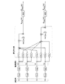
図2は、復調デジタル信号処理部Aの構成図である。図2に示す復調デジタル信号処理部Aは、MIMO等化器として動作する。復調デジタル信号処理部Aは、式(8)及び式(9)に基づいて受信信号を復調する。 FIG. 2 is a configuration diagram of the demodulated digital signal processing unit A. The demodulated digital signal processing unit A shown in FIG. 2 operates as a MIMO equalizer. The demodulated digital signal processing unit A demodulates the received signal based on the equations (8) and (9).
復調デジタル信号処理部Aは、ADC531−1〜531−4によりデジタル信号に変換されたX偏波の受信複素信号SX4の実数成分XI及び虚数成分XQと、Y偏波の受信複素信号SY4の実数成分YI及び虚数成分YQとを入力する。復調デジタル信号処理部Aは、実数成分XI、虚数成分XQ、実数成分YI及び虚数成分YQのそれぞれに対して、受信機50の周波数特性を補償するインパルス応答と波長分散補償用の複素インパルス応答hCD −1を畳み込み、周波数オフセット補償用位相回転を施す。これにより、X偏波成分、Y偏波成分それぞれについて2つの複素信号が出力される。続いて、復調デジタル信号処理部Aは、2つの複素信号それぞれの位相共役を生成し、X偏波成分及びY偏成分波それぞれについて、実数成分XI、虚数成分XQ、実数成分YI及び虚数成分YQと、それらそれぞれの位相共役との8つの信号を入力とする。これにより、受信機50の適応等化器524で、光ファイバ伝送路30及び受信機50で生じたインペアメントに加えて、送信機10で生じたIQインバランスやIQレーン間スキュー、IQ変調器141−1、141−2のバイアスずれ等を動的に補償することが可能になり、受信信号が高品質化される。
Demodulating the digital signal processing unit A includes a real component XI and imaginary components XQ of the received complex signal S X4 of the X polarized wave is converted into a digital signal by ADC531-1~531-4, the reception of the Y polarization complex signal S Y4 The real number component YI and the imaginary number component YQ of are input. The demodulated digital signal processing unit A has an impulse response for compensating the frequency characteristics of the
具体的には、復調デジタル信号処理部Aは、X偏波成分の受信複素信号RX4の実数成分XIに受信機50の周波数特性を補償するインパルス応答hRXI及び波長分散補償用のインパルス応答hCD −1を施し、X偏波成分の受信複素信号RX4の虚数成分XQに受信機50の周波数特性を補償するインパルス応答hRXQ及び波長分散補償用のインパルス応答hCD −1を施す。同様に、復調デジタル信号処理部Aは、Y偏波成分の受信複素信号RY4の実数成分YIに受信機50の周波数特性を補償するインパルス応答hRYI及び波長分散補償用のインパルス応答hCD −1を施し、Y偏波成分の受信複素信号RY4の虚数成分YQに受信機50の周波数特性を補償するインパルス応答hRYQ及び波長分散補償用のインパルス応答hCD −1を施す。復調デジタル信号処理部Aは、受信機50の周波数特性を補償するインパルス応答及び波長分散補償用のインパルス応答が畳み込まれた実数成分XI、虚数成分XQ、実数成分YI、虚数成分YQのそれぞれを4つに分岐し、分岐した4つの信号のうち2つの信号をそのまま適応等化部534に入力し、残りの2つの信号を位相共役信号に変換して適応等化部534に入力する。
Specifically, the demodulated digital signal processing unit A has an impulse response h RXI that compensates the frequency characteristic of the
適応等化部534は、インパルス応答h1が畳み込まれた実数成分XIと、インパルス応答h5が畳み込まれた虚数成分XQと、インパルス応答h9が畳み込まれた実数成分YIと、インパルス応答h13が畳み込まれた虚数成分YQとを加算した後、周波数オフセットexp(jωx(n/T))を施す。nは、シンボル間隔、Tはシンボルの周期を表す。さらに、適応等化部534は、インパルス応答h2が畳み込まれた実数成分位相共役XI*と、インパルス応答h6が畳み込まれた虚数成分位相共役XQ*と、インパルス応答h10が畳み込まれた実数成分位相共役YI*と、インパルス応答h14が畳み込まれた虚数成分位相共役YQ*とを加算した後、周波数オフセットexp(−jωx(n/T))を施す。適応等化部534は、周波数オフセットexp(jωx(n/T))が施された加算信号と、周波数オフセットexp(−jωx(n/T))が施された加算信号とを加算し、X偏波成分の受信信号を得る。適応等化部534は、得られたX偏波成分の受信信号に、X偏波成分のバイアスずれをキャンセルするための送信データバイアス補正信号CXを加算(又は減算)し、歪み補正を行ったX偏波成分の受信信号XRsig(n)を得る。デマッピング部536は、受信信号XRsig(n)にシンボル判定を行った結果得られた受信信号X^Rsig(n)を出力する。
一方、適応等化部534は、インパルス応答h3が畳み込まれた実数成分XIと、インパルス応答h7が畳み込まれた虚数成分XQと、インパルス応答h11が畳み込まれた実数成分YIと、インパルス応答h15が畳み込まれた虚数成分YQとを加算した後、周波数オフセットexp(jωy(n/T))を施す。さらに、適応等化部534は、インパルス応答h4が畳み込まれた実数成分位相共役XI*と、インパルス応答h12が畳み込まれた虚数成分位相共役XQ*と、インパルス応答h16が畳み込まれた実数成分位相共役YI*と、インパルス応答h14が畳み込まれた虚数成分位相共役YQ*とを加算した後、周波数オフセットexp(−jωy(n/T))を施す。適応等化部534は、周波数オフセットexp(jωy(n/T))が施された加算信号と、周波数オフセットexp(−jωy(n/T))が施された加算信号とを加算し、Y偏波成分の受信信号を得る。適応等化部534は、得られたY偏波成分の受信信号に、Y偏波成分のバイアスずれをキャンセルするための送信データバイアス補正信号CYを加算(又は減算)し、歪み補正を行ったX偏波成分の受信信号YRsig(n)を得る。デマッピング部536は、受信信号YRsig(n)にシンボル判定を行った結果得られた受信信号Y^Rsig(n)を出力する。
On the other hand, the
なお、波長分散補償用の複素インパルス応答hCD −1、インパルス応答h1〜h16、及び、周波数オフセットexp(jωxn/T)、exp(−jωxn/T)、exp(jωyn/T)、exp(−jωyn/T)は適応的かつ動的に変更される。受信機50は、これらの値を任意の方法により取得する。
The complex impulse response h CD -1 for wavelength dispersion compensation, the impulse response h 1 to h 16 , and the frequency offset exp (jω xn / T), exp (−jω xn / T), exp (jω yn / T). ), Exp (-jω yn / T) is changed adaptively and dynamically. The
なお、インパルス応答hRXI、hRXQ、hRYI、hRYQの畳み込みは、図1に示すフロントエンド補正部532の処理に対応し、波長分散補償用のインパルス応答hCD −1の畳み込みは波長分散補償部533の処理に対応する。送信データバイアス補正信号CX、CYの加算(又は減算)は、周波数及び位相オフセット補償部535の機能に対応する。
The convolution of the impulse response h RXI , h RXQ , h RYI , and h RYQ corresponds to the processing of the front
図3は、従来技術を用いた復調デジタル信号処理部の構成図である。図3に示す構成でも、受信機において生じるIQインバランス・スキューを補償可能である。しかし、複素数4×2MIMO等化器では、送受信器間の光源に波長オフセット及び位相オフセットが存在した場合、送信器で生じた波形歪みを補償できない。換言すれば、補償に必要なタップ(h)の種類(未知数の数)に比べて、入力信号の次元(連立方程式の数)が不足している。
FIG. 3 is a configuration diagram of a demodulated digital signal processing unit using the prior art. The configuration shown in FIG. 3 can also compensate for the IQ imbalance skew that occurs in the receiver. However, the
具体的には、X偏波の受信複素信号Sx4は、式(6)に示すように、複素信号Sx0、SY0及びその共役Sx0 *、SY0 *に異なる複素インパルス応答を畳み込み、周波数オフセットexp(jωxn)又はexp(−jωxn)を乗じた独立な8個の複素項とバイアス項CbiasXの加算によって表現できる。同様に、Y偏波の受信複素信号SY4は、式(7)に示すように、複素信号SX0、SY0及びその共役SX0 *、SY0 *に異なる複素インパルス応答を畳み込み、周波数オフセットexp(jωyn)又はexp(−jωyn)を乗じた独立な8個の複素項とバイアス項CbiasYとの加算によって表現できる。ゆえに、行列表現式(5)のように、ファイバ伝搬後に受信した偏波多重信号は、16個の独立な複素項w11〜w44と、2つのバイアス項Cbiasx、Cbiasyとで表現できる。従って、複素信号Sx0、SY0は、受信複素信号Sx4、SY4及びその共役Sx0 *、SY0 *に、正負の周波数オフセットを乗じ、適当な16個の異なるインパルス応答h1〜h16を畳みこむことで表現可能である。上述したように、インパルス応答h1〜h16は、行列Wの逆行列の要素である。 Specifically, the received complex signal S x4 the X polarization, as shown in equation (6), the complex signal S x0, S Y0 and its conjugate S x0 *, convolution S Y0 * different complex impulse response, It can be expressed by the addition of eight independent complex terms multiplied by the frequency offset exp (jω x n) or exp (−jω x n) and the bias term C biasX . Similarly, the received complex signal S Y4 of the Y polarization, as shown in equation (7), the complex signal S X0, S Y0 and its conjugate S X0 *, convolution S Y0 * different complex impulse response, the frequency offset It can be expressed by the addition of eight independent complex terms multiplied by exp (jω y n) or exp (−j ω y n) and the bias term C biasY . Thus, as in the matrix expression (5), polarization multiplexing signal received after fiber propagation, the 16 independent complex term w 11 to w 44, 2 two bias term C Biasx, can be represented by a C Biasy .. Therefore, the complex signals S x0 , SY0 are the received complex signals S x4 , SY4 and their conjugates S x0 * , SY0 * multiplied by the positive and negative frequency offsets, and 16 appropriate impulse responses h 1 to h. It can be expressed by folding 16 . As described above, the impulse responses h 1 to h 16 are elements of the inverse matrix of the matrix W.
しかしながら、図3に示すような従来技術を適用した構成では、式(5)において、周波数オフセットexp(jωxn)のみを考慮したモデルを用いているため、一方の周波数オフセットのみを乗じて、exp(jωxn)Sx4、exp(jωxn)SY4とその共役exp(−jωxn)Sx4 *、exp(−jωxn)SY4 *項のみを使って送信信号を表現している。よって、hrx、grxで表現される受信機のIQインバランス及びスキューは補正可能であったが、送信機での歪みは補正できない。 However, in the configuration to which the conventional technique is applied as shown in FIG. 3, since the model in which only the frequency offset exp (jω x n) is considered is used in the equation (5), only one frequency offset is multiplied. Express the transmitted signal using only the exp (jω x n) S x4 , exp (jω x n) S Y4 and its conjugate exp (-jω x n) S x4 * , exp (-jω x n) S Y4 * terms. are doing. Therefore, the IQ imbalance and skew of the receiver expressed by h rx and gr x can be corrected, but the distortion in the transmitter cannot be corrected.
図4は、適応等化処理の品質に関する実験結果を示す図である。図4(a)は、従来技術を用いた受信機における受信信号のコンスタレーションを示し、図4(b)は、本実施形態の受信機50における受信信号のコンスタレーションを示す。受信信号は、波長分散1360ps/nmのシングルモードファイバ(SMF)を80km伝送した偏波多重16QAM(Quadrature Amplitude Modulation)信号である。周波数オフセットは160[MHz]とした。また、受信機内スキューについては、XI−XQを10[ps]、YI−YQを25[ps]とした。
FIG. 4 is a diagram showing the experimental results regarding the quality of the adaptive equalization process. FIG. 4A shows the constellation of the received signal in the receiver using the prior art, and FIG. 4B shows the constellation of the received signal in the
図4(a)に示すように、従来技術を用いた受信機では、変調器バイアスのずれの影響のため、ひし形の歪みが残っている。BER(Bit Error Rate:ビット誤り率)は、7.4×10⁻⁴であった。一方、図4(b)に示すように、本実施形態の受信機50では、正方形で歪みのない信号を得ることができた。BERは、1.3×10⁻⁴であり、従来技術を用いた受信機よりも低かった。
As shown in FIG. 4A, in the receiver using the prior art, diamond distortion remains due to the influence of the displacement of the modulator bias. The BER (Bit Error Rate) was 7.4 × 10 -4 . On the other hand, as shown in FIG. 4B, the
上記の実験結果から、本実施形態によれば、従来技術では除去できなかった変調器バイアスのずれの影響(ひし形の歪み)を除去し、正方形で歪みの無い信号を得ることが可能であることがわかる。 From the above experimental results, according to the present embodiment, it is possible to remove the influence of the displacement of the modulator bias (diamond distortion) that could not be removed by the prior art, and to obtain a square and distortion-free signal. I understand.
続いて、本発明の第2の実施形態について説明する。図示はしないが、第2の実施形態では、偏波多重信号が空間的にN多重(N≧2)された場合について説明する。本実施形態のデジタルコヒーレント光伝送システムの基本的なシステム構成は、図1に示す第1の実施形態のデジタルコヒーレント光伝送システム1と同様である。本実施形態のデジタルコヒーレント光伝送システムが、図1に示すデジタルコヒーレント光伝送システム1と異なる点は、送信機10が空間的にN多重された偏波多重信号を送信する点、WDM合波器20及びWDM分波器40に加え、モード合分波器などの空間多重・分離用のデバイスが挿入される点、及び、受信機50において、光フロントエンド520が空間多重数分配置され、MIMO等化器(復調デジタル信号処理部A)の入力および複素インパルス応答の数が16N2に増加し、N組の偏波多重信号が復調される点である。
Subsequently, a second embodiment of the present invention will be described. Although not shown, the second embodiment describes a case where the polarization multiplex signal is spatially N-multiplexed (N ≧ 2). The basic system configuration of the digital coherent optical transmission system of the present embodiment is the same as that of the digital coherent
空間的にN多重された偏波多重信号は、例えば、マルチコアファイバやマルチモード等により受信機50に送信される。モード数Nの空間多重伝送においては、上記の式(5)と同様にして、4N×4Nの行列により送受信機を含めた伝送路の状態を記述することができる。したがって、受信機のMIMO等化器における複素インパルス応答の数を16N2とすれば、空間多重伝送の場合においても、送信機で生じた歪みを受信機におけるデジタル信号処理で補償可能になる。
The spatially N-multiplexed polarization-multiplexed signal is transmitted to the
具体的には、復調デジタル信号処理部Aは、以下のように動作する。光フロントエンド520が出力するi番目(iは1以上N以下の整数)の偏波多重受信信号のX偏波成分のI成分信号を実数成分XIi、Q成分信号を虚数成分XQiとし、Y偏波成分のI成分信号を実数成分YIi、Q成分信号を虚数成分YQiとする。復調デジタル信号処理部Aは、i番目の偏波多重受信信号の実数成分XIi、虚数成分XQi、実数成分YIi、及び、実数成分YQiのそれぞれに、各成分に応じて、受信機の周波数特性を補償するインパルス応答及び波長分散補償用の複素インパルス応答を畳み込む。復調デジタル信号処理部Aは、畳み込みが行われた実数成分XIi、虚数成分XQi、実数成分YIi、及び、虚数成分YQiのそれぞれを4N個に分岐する。復調デジタル信号処理部Aは、分岐した4N個の信号のうち2N個の信号をそのまま適応等化部534に入力し、残りの2N個の信号を位相共役信号に変換して適応等化部534に入力する。実数成分XIi、虚数成分XQi、実数成分YIi、虚数成分YQiそれぞれの位相共役を、実数成分位相共役XIi *、虚数成分位相共役XQi *、実数成分位相共役YIi *、虚数成分位相共役YQi *とする。実数成分XIi、虚数成分XQi、実数成分YIi、虚数成分YQi、実数成分位相共役XIi *、虚数成分位相共役XQi *、実数成分位相共役YIi *、及び、虚数成分位相共役YQi *からなる2N個の組それぞれは、N個の偏波多重受信信号のX偏波成分及びY偏波成分に対応する。
Specifically, the demodulated digital signal processing unit A operates as follows. Let the I component signal of the X polarization component of the i-th (i is an integer of 1 or more and N or less) polarization multiplex reception signal output by the optical
適応等化部534は、2N個の実数成分XI1〜XIN、虚数成分XQ1〜XQN、実数成分YI1〜YIN、虚数成分YQ1〜YQN、実数成分位相共役XI1 *〜XIN *、虚数成分位相共役XQ1 *〜XQN *、実数成分位相共役YI1 *〜YIN *、虚数成分位相共役YQ1 *〜YQN *のそれぞれに、インパルス応答を畳み込む。各成分及び各位相共役に畳み込むインパルス応答は、4N×4Nで表された式(5)の行列Wの逆行列の要素で表される。適応等化部534は、各偏波多重受信信号の偏波ごとに、該偏波及び各成分に応じたインパルス応答が畳み込まれた実数成分XI1〜XIN、虚数成分XQ1〜XQN、実数成分YI1〜YIN、及び、虚数成分YQ1〜YQNを加算し、周波数オフセット補償用の位相回転を施して第一加算信号を生成する。同様に、適応等化部534は、各偏波多重受信信号の偏波ごとに、該偏波及び各位相共役に応じたインパルス応答が畳み込まれた実数成分位相共役XI1 *〜XIN *、虚数成分位相共役XQ1 *〜XQN *、実数成分位相共役YI1 *〜YIN *、及び、虚数成分位相共役YQ1 *〜YQN *を加算し、周波数オフセット補償用の位相回転とは逆の位相回転を施して第二加算信号を生成する。適応等化部534は、各偏波多重受信信号の偏波ごとに、該偏波について生成された第一加算信号及び第二加算信号を加算して受信信号を得ると、該偏波の送信データバイアス補正信号を加算(又は減算)して歪み補正を行う。
以上説明した実施形態によれば、受信機が備える信号処理装置は、第一補償部と、入力信号生成部と、等化部と、第二補償部とを備える。受信機が、シングルモードファイバ伝送用の偏波多重信号を受信する場合、例えば、信号処理装置はデジタル信号処理部530であり、第一補償部はフロントエンド補正部532及び波長分散補償部533であり、入力信号生成部は波長分散補償部533であり、等化部は適応等化部534であり、第二補償部は周波数及び位相オフセット補償部535である。
According to the embodiment described above, the signal processing device included in the receiver includes a first compensation unit, an input signal generation unit, an equalization unit, and a second compensation unit. When the receiver receives the polarization multiplex signal for single mode fiber transmission, for example, the signal processing device is the digital
第一補償部は、偏波多重された受信信号の各偏波の実数成分及び虚数成分のそれぞれに、受信機の周波数特性を補償するインパルス応答及び波長分散補償用の複素インパルス応答を畳み込む。入力信号生成部は、各偏波ごとに、畳み込みが行われた各偏波の実数成分及び虚数成分と畳み込みが行われた各偏波の実数成分及び虚数成分それぞれの位相共役とを入力信号として生成する。等化部は、各偏波ごとに、入力信号に含まれる各偏波の実数成分及び虚数成分それぞれに複素インパルス応答を乗算したのち加算し、さらに周波数オフセット補償用の位相回転を施した第一加算信号と、入力信号に含まれる各偏波の実数成分の位相共役及び虚数成分の位相共役それぞれに複素インパルス応答を乗算したのち加算し、さらに周波数オフセット補償用の位相回転とは逆の位相回転を施した第二加算信号とを生成する。第二補償部は、第一加算信号と第二加算信号とを加算した信号に、送信データバイアス補正信号を加算又は減算する。 The first compensation unit convolves an impulse response for compensating the frequency characteristics of the receiver and a complex impulse response for wavelength dispersion compensation in each of the real number component and the imaginary number component of each polarization of the polarization-multiplexed reception signal. For each polarization, the input signal generator uses the real and imaginary components of each polarized light that has been convolved and the phase conjugation of the real and imaginary components of each polarized light that has been convolved as input signals. Generate. For each polarization, the equalization unit multiplies the real and imaginary components of each polarization contained in the input signal by the complex impulse response, adds them, and then performs phase rotation for frequency offset compensation. The addition signal, the phase conjugate of the real component of each polarization contained in the input signal, and the phase conjugate of the imaginary component are multiplied by the complex impulse response and then added, and the phase rotation is opposite to the phase rotation for frequency offset compensation. Is generated with the second addition signal. The second compensation unit adds or subtracts the transmission data bias correction signal to the signal obtained by adding the first addition signal and the second addition signal.
あるいは、信号処理装置を備える受信機は、空間的にN多重された偏波多重受信信号を受信する。第一補償部は、空間的にN(Nは2以上の整数)多重された偏波多重受信信号に含まれる各偏波の実数成分及び虚数成分のそれぞれに、受信機の周波数特性を補償するインパルス応答及び波長分散補償用の複素インパルス応答を畳み込む。入力信号生成部は、N個の偏波多重受信信号それぞれの各偏波ごとに、N個の偏波多重受信信号それぞれの畳み込みが行われた各偏波の実数成分及び虚数成分とN個の偏波多重受信信号それぞれの畳み込みが行われた各偏波の実数成分及び虚数成分それぞれの位相共役とを入力信号として生成する。これにより、各偏波多重受信信号の偏波成分ごとに、8N個の信号が入力信号として生成され、X偏波及びY偏波成分からなる1つの偏波多重受信信号については、16N個の信号が入力信号となる。等化部は、N個の偏波多重受信信号それぞれの各偏波ごとに、該偏波について生成された入力信号に含まれる各偏波の実数成分及び虚数成分それぞれに複素インパルス応答を乗算したのち加算し、さらに周波数オフセット補償用の位相回転を施して第一加算信号を生成する。また、等化部は、N個の偏波多重受信信号それぞれの各偏波ごとに、該偏波について生成された入力信号に含まれるN個の偏波の実数成分の位相共役及び虚数成分の位相共役それぞれに複素インパルス応答を乗算したのち加算し、さらに周波数オフセット補償用の位相回転とは逆の位相回転を施した第二加算信号とを生成する。第二補償部は、N個の偏波多重受信信号それぞれの各偏波ごとに、該偏波について生成された第一加算信号と第二加算信号とを加算した信号に、送信データバイアス補正信号を加算又は減算する。 Alternatively, the receiver equipped with the signal processing device receives the spatially N-multiplexed polarization multiplex reception signal. The first compensator compensates the frequency characteristics of the receiver for each of the real and imaginary components of each polarization contained in the polarization multiplex reception signal spatially N (N is an integer of 2 or more). Convolve the impulse response and the complex impulse response for wavelength dispersion compensation. The input signal generation unit has N polarization components, imaginary components, and N polarization components of each polarization in which each polarization of the N polarization multiple reception signals is convoluted for each polarization of each of the N polarization multiple reception signals. The polarization multiplex reception signal is generated as an input signal with the phase conjugate of each of the real and imaginary components of each polarized light that has been convoluted. As a result, 8N signals are generated as input signals for each polarization component of each polarization multiple reception signal, and 16N signals are generated for one polarization multiple reception signal consisting of X polarization and Y polarization components. The signal becomes the input signal. The equalizing unit multiplies each of the real and imaginary components of each polarization contained in the input signal generated for the polarization by a complex impulse response for each polarization of each of the N polarization multiplex reception signals. After that, the signals are added, and then phase rotation for frequency offset compensation is performed to generate the first addition signal. Further, the equalizing unit is for each polarization of each of the N polarization multiplex reception signals, and the phase conjugation and imaginary component of the real component of the N polarization included in the input signal generated for the polarization. Each phase conjugation is multiplied by a complex impulse response and then added to generate a second added signal that is subjected to a phase rotation opposite to the phase rotation for frequency offset compensation. The second compensating unit adds a transmission data bias correction signal to the signal obtained by adding the first addition signal and the second addition signal generated for each polarization of each of the N polarization multiplex reception signals. Is added or subtracted.
なお、複素インパルス応答は、動的に更新される。また、第二補償部は、送信データバイアス補正信号を適応的に加算又は減算する。 The complex impulse response is dynamically updated. In addition, the second compensation unit adaptively adds or subtracts the transmission data bias correction signal.
以上、この発明の実施形態について図面を参照して詳述してきたが、具体的な構成はこの実施形態に限られるものではなく、この発明の要旨を逸脱しない範囲の設計等も含まれる。 Although the embodiments of the present invention have been described in detail with reference to the drawings, the specific configuration is not limited to this embodiment, and the design and the like within a range not deviating from the gist of the present invention are also included.
1…デジタルコヒーレント光伝送システム
10…送信機
20…WDM合波器
30…光ファイバ伝送路
31…光増幅器
40…WDM分波器
50…受信機
100…送信部
110…デジタル信号処理部
111…符号化部
112…マッピング部
113…トレーニング信号挿入部
114…サンプリング周波数変更部
115…波形整形部
116…予等化部
117−1〜117−4デジタル−アナログ変換器
120…変調器ドライバ
121−1〜121−4…アンプ
130…光源
140…集積モジュール
141−1、141−2…IQ変調器
142…偏波合成部
500…受信部
510…局部発振光源
520…光フロントエンド
521…偏波分離部
522−1、522−2…光90度ハイブリッドカプラ
523−1〜523−4…BPD
524−1〜524−4…アンプ
530…デジタル信号処理部
531−1〜531−4…アナログ−デジタル変換器
532…フロントエンド補正部
533…波長分散補償部
534…適応等化部
535…周波数及び位相オフセット補償部
536…デマッピング部
537…復号部
1 ... Digital coherent
524-1 to 524-4 ...
Claims (7)
各偏波ごとに、畳み込みが行われた各偏波の前記実数成分及び前記虚数成分と畳み込みが行われた各偏波の前記実数成分及び前記虚数成分それぞれの位相共役とを入力信号として生成する入力信号生成ステップと、
各偏波ごとに、前記入力信号に含まれる各偏波の前記実数成分及び前記虚数成分それぞれに複素インパルス応答を乗算したのち加算し、さらに周波数オフセット補償用の位相回転を施した第一加算信号と、前記入力信号に含まれる各偏波の前記実数成分の前記位相共役及び前記虚数成分の前記位相共役それぞれに複素インパルス応答を乗算したのち加算し、さらに周波数オフセット補償用の前記位相回転とは逆の位相回転を施した第二加算信号とを生成する等化ステップと、
各偏波ごとに、前記第一加算信号と前記第二加算信号とを加算した信号に、送信データバイアス補正信号を加算又は減算する第二補償ステップと、
を有する信号処理方法。 The first compensation step of convolving the impulse response for compensating the frequency characteristics of the receiver and the complex impulse response for wavelength dispersion compensation into each of the real and imaginary components of each polarization of the polarization-multiplexed reception signal.
For each polarized light, the real number component and the imaginary number component of each convolved polarized light and the phase conjugate of the real number component and the imaginary number component of each convolved polarized light are generated as input signals. Input signal generation step and
For each polarization, the first addition signal is added after multiplying each of the real number component and the imaginary number component of each polarization contained in the input signal by a complex impulse response, and further subjected to phase rotation for frequency offset compensation. And the phase conjugate of the real number component of each polarized light included in the input signal and the phase conjugate of the imaginary component are each multiplied by a complex impulse response and then added, and further, the phase rotation for frequency offset compensation is An equalization step to generate a second addition signal with opposite phase rotation,
For each polarization, a second compensation step of adding or subtracting a transmission data bias correction signal to the signal obtained by adding the first addition signal and the second addition signal, and
Signal processing method having.
請求項1に記載の信号処理方法。 The receiver receives the polarization-multiplexed reception signal by an optical signal.
The signal processing method according to claim 1.
N個の前記偏波多重受信信号それぞれの各偏波ごとに、N個の前記偏波多重受信信号それぞれの畳み込みが行われた各偏波の前記実数成分及び前記虚数成分とN個の前記偏波多重受信信号それぞれの畳み込みが行われた各偏波の前記実数成分及び前記虚数成分それぞれの位相共役とを入力信号として生成する入力信号生成ステップと、
N個の前記偏波多重受信信号それぞれの各偏波ごとに、該偏波の前記入力信号に含まれる各偏波の前記実数成分及び前記虚数成分それぞれに複素インパルス応答を乗算したのち加算し、さらに周波数オフセット補償用の位相回転を施した第一加算信号を生成する処理と、N個の前記偏波多重受信信号それぞれの各偏波ごとに、該偏波の前記入力信号に含まれる各偏波の前記実数成分の前記位相共役及び前記虚数成分の前記位相共役それぞれに複素インパルス応答を乗算したのち加算し、さらに周波数オフセット補償用の前記位相回転とは逆の位相回転を施した第二加算信号を生成する処理とを行う等化ステップと、
N個の前記偏波多重受信信号それぞれの各偏波ごとに、該偏波について生成された前記第一加算信号と前記第二加算信号とを加算した信号に、送信データバイアス補正信号を加算又は減算する第二補償ステップと、
を有する信号処理方法。 Polarized polarization that is spatially N (N is an integer of 2 or more) Multiplexed Impulse response and wavelength dispersion compensation that compensate for the frequency characteristics of the receiver for each of the real and imaginary components of each polarization contained in the received signal. First compensation step to convolve the complex impulse response for
For each polarization of each of the N polarization multiplex reception signals, the real component and the imaginary component of each polarization in which the N polarization multiplex reception signals are convoluted, and the N biases. An input signal generation step of generating as an input signal the real component and the phase conjugate of each of the imaginary components of each polarized light in which each of the wave multiplex received signals is convoluted.
For each polarization of each of the N polarization multiplex reception signals, the real component and the imaginary component of each polarization included in the input signal of the polarization are multiplied by a complex impulse response and then added. Further, a process of generating a first addition signal subjected to phase rotation for frequency offset compensation, and each polarization included in the input signal of the polarization for each polarization of each of the N polarization multiplex reception signals. The phase conjugate of the real component of the wave and the phase conjugate of the imaginary component are each multiplied by a complex impulse response and then added, and further subjected to a phase rotation opposite to the phase rotation for frequency offset compensation. An equalization step that performs the process of generating a signal,
For each polarization of each of the N polarization multiplex reception signals, a transmission data bias correction signal is added or added to a signal obtained by adding the first addition signal and the second addition signal generated for the polarization. The second compensation step to subtract and
Signal processing method having.
前記第二補償ステップにおいては、前記送信データバイアス補正信号を適応的に加算又は減算する、
請求項1から請求項3のいずれか一項に記載の信号処理方法。 The complex impulse response is dynamically updated.
In the second compensation step, the transmission data bias correction signal is adaptively added or subtracted.
The signal processing method according to any one of claims 1 to 3.
各偏波ごとに、畳み込みが行われた各偏波の前記実数成分及び前記虚数成分と畳み込みが行われた各偏波の前記実数成分及び前記虚数成分それぞれの位相共役とを入力信号として生成する入力信号生成部と、
各偏波ごとに、前記入力信号に含まれる各偏波の前記実数成分及び前記虚数成分それぞれに複素インパルス応答を乗算したのち加算し、さらに周波数オフセット補償用の位相回転を施した第一加算信号と、前記入力信号に含まれる各偏波の前記実数成分の前記位相共役及び前記虚数成分の前記位相共役それぞれに複素インパルス応答を乗算したのち加算し、さらに周波数オフセット補償用の前記位相回転とは逆の位相回転を施した第二加算信号とを生成する等化部と、
各偏波ごとに、前記第一加算信号と前記第二加算信号とを加算した信号に、送信データバイアス補正信号を加算又は減算する第二補償部と、
を備える信号処理装置。 A first compensator that convolves an impulse response that compensates for the frequency characteristics of the receiver and a complex impulse response for wavelength dispersion compensation into each of the real and imaginary components of each polarization of the polarized and multiplexed reception signal.
For each polarized light, the real number component and the imaginary number component of each convolved polarized light and the phase conjugate of the real number component and the imaginary number component of each convolved polarized light are generated as input signals. Input signal generator and
For each polarization, the first addition signal is added after multiplying each of the real number component and the imaginary number component of each polarization contained in the input signal by a complex impulse response, and further subjected to phase rotation for frequency offset compensation. And the phase conjugate of the real number component of each polarized light included in the input signal and the phase conjugate of the imaginary component are each multiplied by a complex impulse response and then added, and further, the phase rotation for frequency offset compensation is An equalizer that generates a second addition signal that has undergone reverse phase rotation,
For each polarization, a second compensator that adds or subtracts a transmission data bias correction signal to the signal obtained by adding the first addition signal and the second addition signal, and
A signal processing device comprising.
N個の前記偏波多重受信信号それぞれの各偏波ごとに、N個の前記偏波多重受信信号それぞれの畳み込みが行われた各偏波の前記実数成分及び前記虚数成分とN個の前記偏波多重受信信号それぞれの畳み込みが行われた各偏波の前記実数成分及び前記虚数成分それぞれの位相共役とを入力信号として生成する入力信号生成部と、
N個の前記偏波多重受信信号それぞれの各偏波ごとに、該偏波の前記入力信号に含まれる各偏波の前記実数成分及び前記虚数成分それぞれに複素インパルス応答を乗算したのち加算し、さらに周波数オフセット補償用の位相回転を施した第一加算信号を生成する処理と、N個の前記偏波多重受信信号それぞれの各偏波ごとに、該偏波の前記入力信号に含まれる各偏波の前記実数成分の前記位相共役及び前記虚数成分の前記位相共役それぞれに複素インパルス応答を乗算したのち加算し、さらに周波数オフセット補償用の前記位相回転とは逆の位相回転を施した第二加算信号を生成する処理とを行う等化部と、
N個の前記偏波多重受信信号それぞれの各偏波ごとに、該偏波について生成された前記第一加算信号と前記第二加算信号とを加算した信号に、送信データバイアス補正信号を加算又は減算する第二補償部と、
を備える信号処理装置。 Polarized polarization that is spatially N (N is an integer of 2 or more) Multiplexed Impulse response and wavelength dispersion compensation that compensate for the frequency characteristics of the receiver for each of the real and imaginary components of each polarization contained in the received signal. First compensator that convolves the complex impulse response for
For each polarization of each of the N polarization multiplex reception signals, the real component and the imaginary component of each polarization in which the N polarization multiplex reception signals are convoluted, and the N biases. An input signal generator that generates as an input signal the real component and the phase conjugate of each of the imaginary components of each polarized light in which each of the wave multiplex reception signals is convoluted.
For each polarization of each of the N polarization multiplex reception signals, the real component and the imaginary component of each polarization included in the input signal of the polarization are multiplied by a complex impulse response and then added. Further, a process of generating a first addition signal subjected to phase rotation for frequency offset compensation, and each polarization included in the input signal of the polarization for each polarization of each of the N polarization multiplex reception signals. The phase conjugate of the real component of the wave and the phase conjugate of the imaginary component are each multiplied by a complex impulse response and then added, and further subjected to a phase rotation opposite to the phase rotation for frequency offset compensation. An equalizer that performs processing to generate a signal,
For each polarization of each of the N polarization multiplex reception signals, a transmission data bias correction signal is added or added to a signal obtained by adding the first addition signal and the second addition signal generated for the polarization. The second compensation unit to be subtracted and
A signal processing device comprising.
Priority Applications (3)
| Application Number | Priority Date | Filing Date | Title |
|---|---|---|---|
| JP2019036315A JP7128420B2 (en) | 2019-02-28 | 2019-02-28 | Signal processing method, signal processing device and communication system |
| US17/433,149 US11632185B2 (en) | 2019-02-28 | 2020-01-31 | Signal processing method, signal processing apparatus and communication system |
| PCT/JP2020/003727 WO2020175014A1 (en) | 2019-02-28 | 2020-01-31 | Signal processing method, signal processing device, and communication system |
Applications Claiming Priority (1)
| Application Number | Priority Date | Filing Date | Title |
|---|---|---|---|
| JP2019036315A JP7128420B2 (en) | 2019-02-28 | 2019-02-28 | Signal processing method, signal processing device and communication system |
Publications (2)
| Publication Number | Publication Date |
|---|---|
| JP2020141294A true JP2020141294A (en) | 2020-09-03 |
| JP7128420B2 JP7128420B2 (en) | 2022-08-31 |
Family
ID=72239715
Family Applications (1)
| Application Number | Title | Priority Date | Filing Date |
|---|---|---|---|
| JP2019036315A Active JP7128420B2 (en) | 2019-02-28 | 2019-02-28 | Signal processing method, signal processing device and communication system |
Country Status (3)
| Country | Link |
|---|---|
| US (1) | US11632185B2 (en) |
| JP (1) | JP7128420B2 (en) |
| WO (1) | WO2020175014A1 (en) |
Cited By (7)
| Publication number | Priority date | Publication date | Assignee | Title |
|---|---|---|---|---|
| WO2022091452A1 (en) * | 2020-10-28 | 2022-05-05 | 日本電気株式会社 | Communication system, receiver, distortion detection device, method, and computer readable medium |
| WO2022137299A1 (en) * | 2020-12-21 | 2022-06-30 | 日本電信電話株式会社 | Signal detection device, carrier phase restoration device, carrier phase restoration method and carrier phase restoration program |
| WO2022249458A1 (en) * | 2021-05-28 | 2022-12-01 | 日本電気株式会社 | Optical transmission device, system, method, and non-transitory computer-readable medium |
| WO2022259367A1 (en) | 2021-06-08 | 2022-12-15 | 日本電信電話株式会社 | Signal processing method, signal processing device, and communication system |
| WO2023073927A1 (en) * | 2021-10-29 | 2023-05-04 | 日本電気株式会社 | Digital signal processing circuit, method, receiver, and communication system |
| WO2023135869A1 (en) * | 2022-01-13 | 2023-07-20 | 日本電信電話株式会社 | Characteristic measuring device, characteristic measuring method, and computer program |
| WO2023162143A1 (en) * | 2022-02-25 | 2023-08-31 | 日本電気株式会社 | Communication system, receiver, equalizing signal processing circuit, method, and computer-readable medium |
Families Citing this family (5)
| Publication number | Priority date | Publication date | Assignee | Title |
|---|---|---|---|---|
| CN114337843B (en) * | 2021-12-23 | 2023-11-28 | 武汉邮电科学研究院有限公司 | Self-adaptive channel equalization method and system for coherent optical communication |
| WO2023139658A1 (en) * | 2022-01-18 | 2023-07-27 | Nec Corporation | Calibration apparatus, calibration method, and non-transitory computer-readable storage medium |
| WO2023152909A1 (en) * | 2022-02-10 | 2023-08-17 | 日本電信電話株式会社 | Signal processing method, signal processing device, and communication system |
| WO2023152904A1 (en) * | 2022-02-10 | 2023-08-17 | 日本電信電話株式会社 | Signal processing method, signal processing device, and communication system |
| WO2024013791A1 (en) * | 2022-07-11 | 2024-01-18 | 日本電信電話株式会社 | Signal processing device, signal processing method, and computer program |
Citations (3)
| Publication number | Priority date | Publication date | Assignee | Title |
|---|---|---|---|---|
| US20110150478A1 (en) * | 2009-12-18 | 2011-06-23 | Winzer Peter J | Receiver Algorithms for Coherent Detection of Polarization-Multiplexed Optical Signals |
| WO2012108421A1 (en) * | 2011-02-07 | 2012-08-16 | 日本電信電話株式会社 | Digital signal processing device |
| JP2017158028A (en) * | 2016-03-01 | 2017-09-07 | 日本電信電話株式会社 | Signal transmission system |
Family Cites Families (12)
| Publication number | Priority date | Publication date | Assignee | Title |
|---|---|---|---|---|
| DE2961498D1 (en) | 1978-05-08 | 1982-01-28 | Ici Plc | Production of xylene hydrocarbons |
| US7072832B1 (en) * | 1998-08-24 | 2006-07-04 | Mindspeed Technologies, Inc. | System for speech encoding having an adaptive encoding arrangement |
| AU740804B2 (en) * | 1999-07-19 | 2001-11-15 | Nippon Telegraph & Telephone Corporation | OFDM packet communication receiver system |
| US8103711B1 (en) * | 2008-02-27 | 2012-01-24 | University Of Central Florida Research Foundation, Inc. | Dispersion compensation using digital infinite impulse response filtering |
| JP5683237B2 (en) * | 2010-11-29 | 2015-03-11 | 株式会社日立製作所 | Polarization multiplexed optical transmission system, polarization multiplexed optical transmitter, and polarization multiplexed optical receiver |
| US8594515B2 (en) * | 2011-03-03 | 2013-11-26 | Alcatel Lucent | Digital phase conjugation for fiber-optic links |
| US10038507B2 (en) * | 2013-02-13 | 2018-07-31 | Nippon Telegraph And Telephone Corporation | Optical transmission system, phase compensation method, and optical reception apparatus |
| JP6319487B1 (en) * | 2017-03-14 | 2018-05-09 | Nttエレクトロニクス株式会社 | Optical transmission characteristic estimation method, optical transmission characteristic compensation method, optical transmission characteristic estimation system, and optical transmission characteristic compensation system |
| EP3605882B1 (en) * | 2017-04-19 | 2021-05-26 | Mitsubishi Electric Corporation | Optical transmitter, optical receiver, and optical communication system |
| EP3776921A1 (en) * | 2018-03-29 | 2021-02-17 | Cable Television Laboratories, Inc. | Systems and methods for coherent optics in an access network |
| KR102271053B1 (en) * | 2019-10-31 | 2021-06-30 | 고려대학교 산학협력단 | Point scan type imaging apparatus for imaging target object within media witch bring about aberration |
| US11568884B2 (en) * | 2021-05-24 | 2023-01-31 | Invictumtech, Inc. | Analysis filter bank and computing procedure thereof, audio frequency shifting system, and audio frequency shifting procedure |
-
2019
- 2019-02-28 JP JP2019036315A patent/JP7128420B2/en active Active
-
2020
- 2020-01-31 WO PCT/JP2020/003727 patent/WO2020175014A1/en active Application Filing
- 2020-01-31 US US17/433,149 patent/US11632185B2/en active Active
Patent Citations (3)
| Publication number | Priority date | Publication date | Assignee | Title |
|---|---|---|---|---|
| US20110150478A1 (en) * | 2009-12-18 | 2011-06-23 | Winzer Peter J | Receiver Algorithms for Coherent Detection of Polarization-Multiplexed Optical Signals |
| WO2012108421A1 (en) * | 2011-02-07 | 2012-08-16 | 日本電信電話株式会社 | Digital signal processing device |
| JP2017158028A (en) * | 2016-03-01 | 2017-09-07 | 日本電信電話株式会社 | Signal transmission system |
Non-Patent Citations (2)
| Title |
|---|
| FLUDGER C. R. S. ET AL.: "Transmitter Impairment Mitigation and Monitoring for High Baud-Rate, High Order Modulation Systems", 42ND EUROPEAN CONFERENCE AND EXHIBITION ON OPTICAL COMMUNICATIONS, JPN6022029326, September 2016 (2016-09-01), pages 256 - 258, XP055735231, ISSN: 0004827363 * |
| RIOS-MULLER R. ET AL.: "Blind Receiver Skew Compensation and Estimation for Long-Haul Non-Dispersion Managed Systems Using A", JOURNAL OF LIGHTWAVE TECHNOLOGY, vol. 33, no. 7, JPN6022029327, April 2015 (2015-04-01), US, pages 1315 - 1318, XP011575164, ISSN: 0004827364, DOI: 10.1109/JLT.2014.2377582 * |
Cited By (8)
| Publication number | Priority date | Publication date | Assignee | Title |
|---|---|---|---|---|
| WO2022091452A1 (en) * | 2020-10-28 | 2022-05-05 | 日本電気株式会社 | Communication system, receiver, distortion detection device, method, and computer readable medium |
| WO2022137299A1 (en) * | 2020-12-21 | 2022-06-30 | 日本電信電話株式会社 | Signal detection device, carrier phase restoration device, carrier phase restoration method and carrier phase restoration program |
| WO2022249458A1 (en) * | 2021-05-28 | 2022-12-01 | 日本電気株式会社 | Optical transmission device, system, method, and non-transitory computer-readable medium |
| WO2022259367A1 (en) | 2021-06-08 | 2022-12-15 | 日本電信電話株式会社 | Signal processing method, signal processing device, and communication system |
| WO2023073927A1 (en) * | 2021-10-29 | 2023-05-04 | 日本電気株式会社 | Digital signal processing circuit, method, receiver, and communication system |
| WO2023135869A1 (en) * | 2022-01-13 | 2023-07-20 | 日本電信電話株式会社 | Characteristic measuring device, characteristic measuring method, and computer program |
| WO2023135698A1 (en) * | 2022-01-13 | 2023-07-20 | 日本電信電話株式会社 | Characteristic measurement device, characteristic measurement method, and computer program |
| WO2023162143A1 (en) * | 2022-02-25 | 2023-08-31 | 日本電気株式会社 | Communication system, receiver, equalizing signal processing circuit, method, and computer-readable medium |
Also Published As
| Publication number | Publication date |
|---|---|
| US11632185B2 (en) | 2023-04-18 |
| US20220149974A1 (en) | 2022-05-12 |
| JP7128420B2 (en) | 2022-08-31 |
| WO2020175014A1 (en) | 2020-09-03 |
Similar Documents
| Publication | Publication Date | Title |
|---|---|---|
| JP7128420B2 (en) | Signal processing method, signal processing device and communication system | |
| US8913901B2 (en) | System and method for blind equalization and carrier phase recovery in a quadrature amplitude modulated system | |
| US7315575B2 (en) | Equalization strategy for dual-polarization optical transport system | |
| CA3047882C (en) | Optical transmission characteristic estimation method, optical transmission characteristic compensation method, optical transmission characteristic estimation system and optical transmission characteristic compensation system | |
| US9020364B2 (en) | Optical receiver having a signal-equalization capability | |
| US7630650B2 (en) | Multi-level modulation receiving device | |
| JP5850041B2 (en) | Optical receiver, polarization separation device, and optical reception method | |
| JP4968415B2 (en) | DIGITAL FILTER DEVICE, DIGITAL FILTERING METHOD, AND DIGITAL FILTER DEVICE CONTROL PROGRAM | |
| US9667347B2 (en) | Optical transmitter, optical receiver, method of compensating non-linear distortion, and communication apparatus | |
| US8805208B2 (en) | System and method for polarization de-multiplexing in a coherent optical receiver | |
| JP5390607B2 (en) | Pre-equalization transmission system | |
| US8306440B2 (en) | Polarization diversity receiver systems and methods with polarization mode dispersion mitigation | |
| US10148363B2 (en) | Iterative nonlinear compensation | |
| US8666251B2 (en) | Electronic dispersion compensation system and method | |
| US9692521B1 (en) | Polarization pre-compensation technique for polarization-division-multiplexed direct-detection optical communication systems | |
| EP2873182B1 (en) | Method and device for signal processing in an optical communication network | |
| Puerta et al. | Single-wavelength, single-photodiode per polarization 276 Gb/s PDM 8-QAM over 100 km of SSMF | |
| EP4354745A1 (en) | Signal processing method, signal processing device, and communication system | |
| WO2023135869A1 (en) | Characteristic measuring device, characteristic measuring method, and computer program | |
| Noé et al. | Realtime digital signal processing in coherent optical PDM-QPSK and PDM-16-QAM transmission | |
| US20220393771A1 (en) | Mitigation of equalization-enhanced phase noise in a coherent optical receiver | |
| Rosenkranz et al. | Precoding and equalization in digital coherent optical transmission | |
| Chai et al. | Receiver IQ Imbalances and Skew Compensation based on Frequency Domain 4× 2 MIMO Equalizer for PDM-16QAM Systems | |
| JP2018007206A (en) | Multi-carrier optical receiver and optical transmission system | |
| Chung et al. | Effects of carrier phase estimation on front-end IQ mismatch compensation in mode division multiplexed MIMO coherent receiver |
Legal Events
| Date | Code | Title | Description |
|---|---|---|---|
| A621 | Written request for application examination |
Free format text: JAPANESE INTERMEDIATE CODE: A621 Effective date: 20210531 |
|
| TRDD | Decision of grant or rejection written | ||
| A01 | Written decision to grant a patent or to grant a registration (utility model) |
Free format text: JAPANESE INTERMEDIATE CODE: A01 Effective date: 20220719 |
|
| A61 | First payment of annual fees (during grant procedure) |
Free format text: JAPANESE INTERMEDIATE CODE: A61 Effective date: 20220801 |
|
| R150 | Certificate of patent or registration of utility model |
Ref document number: 7128420 Country of ref document: JP Free format text: JAPANESE INTERMEDIATE CODE: R150 |