JP2020140088A - Liquid crystal display device - Google Patents
Liquid crystal display device Download PDFInfo
- Publication number
- JP2020140088A JP2020140088A JP2019035901A JP2019035901A JP2020140088A JP 2020140088 A JP2020140088 A JP 2020140088A JP 2019035901 A JP2019035901 A JP 2019035901A JP 2019035901 A JP2019035901 A JP 2019035901A JP 2020140088 A JP2020140088 A JP 2020140088A
- Authority
- JP
- Japan
- Prior art keywords
- gate
- liquid crystal
- display device
- crystal display
- line
- Prior art date
- Legal status (The legal status is an assumption and is not a legal conclusion. Google has not performed a legal analysis and makes no representation as to the accuracy of the status listed.)
- Pending
Links
Images


Classifications
-
- G—PHYSICS
- G02—OPTICS
- G02F—OPTICAL DEVICES OR ARRANGEMENTS FOR THE CONTROL OF LIGHT BY MODIFICATION OF THE OPTICAL PROPERTIES OF THE MEDIA OF THE ELEMENTS INVOLVED THEREIN; NON-LINEAR OPTICS; FREQUENCY-CHANGING OF LIGHT; OPTICAL LOGIC ELEMENTS; OPTICAL ANALOGUE/DIGITAL CONVERTERS
- G02F1/00—Devices or arrangements for the control of the intensity, colour, phase, polarisation or direction of light arriving from an independent light source, e.g. switching, gating or modulating; Non-linear optics
- G02F1/01—Devices or arrangements for the control of the intensity, colour, phase, polarisation or direction of light arriving from an independent light source, e.g. switching, gating or modulating; Non-linear optics for the control of the intensity, phase, polarisation or colour
- G02F1/13—Devices or arrangements for the control of the intensity, colour, phase, polarisation or direction of light arriving from an independent light source, e.g. switching, gating or modulating; Non-linear optics for the control of the intensity, phase, polarisation or colour based on liquid crystals, e.g. single liquid crystal display cells
- G02F1/133—Constructional arrangements; Operation of liquid crystal cells; Circuit arrangements
- G02F1/1333—Constructional arrangements; Manufacturing methods
- G02F1/13338—Input devices, e.g. touch panels
-
- G—PHYSICS
- G02—OPTICS
- G02F—OPTICAL DEVICES OR ARRANGEMENTS FOR THE CONTROL OF LIGHT BY MODIFICATION OF THE OPTICAL PROPERTIES OF THE MEDIA OF THE ELEMENTS INVOLVED THEREIN; NON-LINEAR OPTICS; FREQUENCY-CHANGING OF LIGHT; OPTICAL LOGIC ELEMENTS; OPTICAL ANALOGUE/DIGITAL CONVERTERS
- G02F1/00—Devices or arrangements for the control of the intensity, colour, phase, polarisation or direction of light arriving from an independent light source, e.g. switching, gating or modulating; Non-linear optics
- G02F1/01—Devices or arrangements for the control of the intensity, colour, phase, polarisation or direction of light arriving from an independent light source, e.g. switching, gating or modulating; Non-linear optics for the control of the intensity, phase, polarisation or colour
- G02F1/13—Devices or arrangements for the control of the intensity, colour, phase, polarisation or direction of light arriving from an independent light source, e.g. switching, gating or modulating; Non-linear optics for the control of the intensity, phase, polarisation or colour based on liquid crystals, e.g. single liquid crystal display cells
- G02F1/133—Constructional arrangements; Operation of liquid crystal cells; Circuit arrangements
- G02F1/136—Liquid crystal cells structurally associated with a semi-conducting layer or substrate, e.g. cells forming part of an integrated circuit
- G02F1/1362—Active matrix addressed cells
- G02F1/136286—Wiring, e.g. gate line, drain line
-
- G—PHYSICS
- G02—OPTICS
- G02F—OPTICAL DEVICES OR ARRANGEMENTS FOR THE CONTROL OF LIGHT BY MODIFICATION OF THE OPTICAL PROPERTIES OF THE MEDIA OF THE ELEMENTS INVOLVED THEREIN; NON-LINEAR OPTICS; FREQUENCY-CHANGING OF LIGHT; OPTICAL LOGIC ELEMENTS; OPTICAL ANALOGUE/DIGITAL CONVERTERS
- G02F1/00—Devices or arrangements for the control of the intensity, colour, phase, polarisation or direction of light arriving from an independent light source, e.g. switching, gating or modulating; Non-linear optics
- G02F1/01—Devices or arrangements for the control of the intensity, colour, phase, polarisation or direction of light arriving from an independent light source, e.g. switching, gating or modulating; Non-linear optics for the control of the intensity, phase, polarisation or colour
- G02F1/13—Devices or arrangements for the control of the intensity, colour, phase, polarisation or direction of light arriving from an independent light source, e.g. switching, gating or modulating; Non-linear optics for the control of the intensity, phase, polarisation or colour based on liquid crystals, e.g. single liquid crystal display cells
- G02F1/133—Constructional arrangements; Operation of liquid crystal cells; Circuit arrangements
- G02F1/1333—Constructional arrangements; Manufacturing methods
- G02F1/1343—Electrodes
- G02F1/134309—Electrodes characterised by their geometrical arrangement
-
- G—PHYSICS
- G02—OPTICS
- G02F—OPTICAL DEVICES OR ARRANGEMENTS FOR THE CONTROL OF LIGHT BY MODIFICATION OF THE OPTICAL PROPERTIES OF THE MEDIA OF THE ELEMENTS INVOLVED THEREIN; NON-LINEAR OPTICS; FREQUENCY-CHANGING OF LIGHT; OPTICAL LOGIC ELEMENTS; OPTICAL ANALOGUE/DIGITAL CONVERTERS
- G02F1/00—Devices or arrangements for the control of the intensity, colour, phase, polarisation or direction of light arriving from an independent light source, e.g. switching, gating or modulating; Non-linear optics
- G02F1/01—Devices or arrangements for the control of the intensity, colour, phase, polarisation or direction of light arriving from an independent light source, e.g. switching, gating or modulating; Non-linear optics for the control of the intensity, phase, polarisation or colour
- G02F1/13—Devices or arrangements for the control of the intensity, colour, phase, polarisation or direction of light arriving from an independent light source, e.g. switching, gating or modulating; Non-linear optics for the control of the intensity, phase, polarisation or colour based on liquid crystals, e.g. single liquid crystal display cells
- G02F1/133—Constructional arrangements; Operation of liquid crystal cells; Circuit arrangements
- G02F1/136—Liquid crystal cells structurally associated with a semi-conducting layer or substrate, e.g. cells forming part of an integrated circuit
- G02F1/1362—Active matrix addressed cells
- G02F1/1368—Active matrix addressed cells in which the switching element is a three-electrode device
-
- G—PHYSICS
- G06—COMPUTING; CALCULATING OR COUNTING
- G06F—ELECTRIC DIGITAL DATA PROCESSING
- G06F3/00—Input arrangements for transferring data to be processed into a form capable of being handled by the computer; Output arrangements for transferring data from processing unit to output unit, e.g. interface arrangements
- G06F3/01—Input arrangements or combined input and output arrangements for interaction between user and computer
- G06F3/03—Arrangements for converting the position or the displacement of a member into a coded form
- G06F3/041—Digitisers, e.g. for touch screens or touch pads, characterised by the transducing means
- G06F3/0412—Digitisers structurally integrated in a display
-
- G—PHYSICS
- G06—COMPUTING; CALCULATING OR COUNTING
- G06F—ELECTRIC DIGITAL DATA PROCESSING
- G06F3/00—Input arrangements for transferring data to be processed into a form capable of being handled by the computer; Output arrangements for transferring data from processing unit to output unit, e.g. interface arrangements
- G06F3/01—Input arrangements or combined input and output arrangements for interaction between user and computer
- G06F3/03—Arrangements for converting the position or the displacement of a member into a coded form
- G06F3/041—Digitisers, e.g. for touch screens or touch pads, characterised by the transducing means
- G06F3/0414—Digitisers, e.g. for touch screens or touch pads, characterised by the transducing means using force sensing means to determine a position
-
- G—PHYSICS
- G06—COMPUTING; CALCULATING OR COUNTING
- G06F—ELECTRIC DIGITAL DATA PROCESSING
- G06F3/00—Input arrangements for transferring data to be processed into a form capable of being handled by the computer; Output arrangements for transferring data from processing unit to output unit, e.g. interface arrangements
- G06F3/01—Input arrangements or combined input and output arrangements for interaction between user and computer
- G06F3/03—Arrangements for converting the position or the displacement of a member into a coded form
- G06F3/041—Digitisers, e.g. for touch screens or touch pads, characterised by the transducing means
- G06F3/0416—Control or interface arrangements specially adapted for digitisers
- G06F3/04166—Details of scanning methods, e.g. sampling time, grouping of sub areas or time sharing with display driving
-
- G—PHYSICS
- G06—COMPUTING; CALCULATING OR COUNTING
- G06F—ELECTRIC DIGITAL DATA PROCESSING
- G06F3/00—Input arrangements for transferring data to be processed into a form capable of being handled by the computer; Output arrangements for transferring data from processing unit to output unit, e.g. interface arrangements
- G06F3/01—Input arrangements or combined input and output arrangements for interaction between user and computer
- G06F3/03—Arrangements for converting the position or the displacement of a member into a coded form
- G06F3/041—Digitisers, e.g. for touch screens or touch pads, characterised by the transducing means
- G06F3/044—Digitisers, e.g. for touch screens or touch pads, characterised by the transducing means by capacitive means
- G06F3/0443—Digitisers, e.g. for touch screens or touch pads, characterised by the transducing means by capacitive means using a single layer of sensing electrodes
-
- G—PHYSICS
- G06—COMPUTING; CALCULATING OR COUNTING
- G06F—ELECTRIC DIGITAL DATA PROCESSING
- G06F3/00—Input arrangements for transferring data to be processed into a form capable of being handled by the computer; Output arrangements for transferring data from processing unit to output unit, e.g. interface arrangements
- G06F3/01—Input arrangements or combined input and output arrangements for interaction between user and computer
- G06F3/03—Arrangements for converting the position or the displacement of a member into a coded form
- G06F3/041—Digitisers, e.g. for touch screens or touch pads, characterised by the transducing means
- G06F3/044—Digitisers, e.g. for touch screens or touch pads, characterised by the transducing means by capacitive means
- G06F3/0446—Digitisers, e.g. for touch screens or touch pads, characterised by the transducing means by capacitive means using a grid-like structure of electrodes in at least two directions, e.g. using row and column electrodes
-
- G—PHYSICS
- G02—OPTICS
- G02F—OPTICAL DEVICES OR ARRANGEMENTS FOR THE CONTROL OF LIGHT BY MODIFICATION OF THE OPTICAL PROPERTIES OF THE MEDIA OF THE ELEMENTS INVOLVED THEREIN; NON-LINEAR OPTICS; FREQUENCY-CHANGING OF LIGHT; OPTICAL LOGIC ELEMENTS; OPTICAL ANALOGUE/DIGITAL CONVERTERS
- G02F2201/00—Constructional arrangements not provided for in groups G02F1/00 - G02F7/00
- G02F2201/12—Constructional arrangements not provided for in groups G02F1/00 - G02F7/00 electrode
- G02F2201/121—Constructional arrangements not provided for in groups G02F1/00 - G02F7/00 electrode common or background
-
- G—PHYSICS
- G02—OPTICS
- G02F—OPTICAL DEVICES OR ARRANGEMENTS FOR THE CONTROL OF LIGHT BY MODIFICATION OF THE OPTICAL PROPERTIES OF THE MEDIA OF THE ELEMENTS INVOLVED THEREIN; NON-LINEAR OPTICS; FREQUENCY-CHANGING OF LIGHT; OPTICAL LOGIC ELEMENTS; OPTICAL ANALOGUE/DIGITAL CONVERTERS
- G02F2201/00—Constructional arrangements not provided for in groups G02F1/00 - G02F7/00
- G02F2201/12—Constructional arrangements not provided for in groups G02F1/00 - G02F7/00 electrode
- G02F2201/123—Constructional arrangements not provided for in groups G02F1/00 - G02F7/00 electrode pixel
Landscapes
- Physics & Mathematics (AREA)
- Engineering & Computer Science (AREA)
- Nonlinear Science (AREA)
- General Physics & Mathematics (AREA)
- General Engineering & Computer Science (AREA)
- Theoretical Computer Science (AREA)
- Crystallography & Structural Chemistry (AREA)
- Mathematical Physics (AREA)
- Chemical & Material Sciences (AREA)
- Optics & Photonics (AREA)
- Microelectronics & Electronic Packaging (AREA)
- Human Computer Interaction (AREA)
- Liquid Crystal (AREA)
- Geometry (AREA)
- Devices For Indicating Variable Information By Combining Individual Elements (AREA)
Abstract
Description
本開示は、液晶表示装置に関する。 The present disclosure relates to a liquid crystal display device.
液晶表示装置は、低消費電力で画像を表示することができるため、テレビ又はモニタ等の画像表示装置として利用されている。液晶表示装置は、行列状に配列された複数の画素の各々に設けられたトランジスタと、行方向に延在する複数のゲート線と、列方向に延在する複数のデータ線とを備える。また、液晶表示装置の額縁領域には、複数のゲート線にゲート信号を供給するゲートドライバと、複数のソース線にデータ信号を供給するソースドライバとが実装される。 Since the liquid crystal display device can display an image with low power consumption, it is used as an image display device such as a television or a monitor. The liquid crystal display device includes transistors provided in each of a plurality of pixels arranged in a matrix, a plurality of gate lines extending in the row direction, and a plurality of data lines extending in the column direction. Further, in the frame area of the liquid crystal display device, a gate driver that supplies gate signals to a plurality of gate lines and a source driver that supplies data signals to a plurality of source lines are mounted.
一般的に、ゲートドライバとソースドライバとは額縁領域の異なる辺に設けられるが、狭額縁化等を目的として、ゲートドライバとソースドライバとを額縁領域の同じ辺に設ける技術も知られている(例えば、特許文献1)。 Generally, the gate driver and the source driver are provided on different sides of the frame area, but there is also known a technique of providing the gate driver and the source driver on the same side of the frame area for the purpose of narrowing the frame. For example, Patent Document 1).
上記のように、ゲートドライバとソースドライバとを額縁領域の同じ辺に設けると、ゲート線が延在する方向の延長上にゲートドライバが存在しなくなるので、ゲート線を行方向に沿って額縁領域にまで引き延ばしたとしても、ゲート線をゲートドライバに接続することができない。 As described above, if the gate driver and the source driver are provided on the same side of the frame area, the gate driver does not exist on the extension in the direction in which the gate line extends, so that the gate line is provided in the frame area along the row direction. Even if it is stretched to, the gate wire cannot be connected to the gate driver.
そこで、ゲート線とゲートドライバとを接続するために、中継配線として、ゲート線と直交する方向に延在するゲート引出線を別途形成して、ゲート引出線を介してゲート線とゲートドライバとを接続することが考えられる。 Therefore, in order to connect the gate wire and the gate driver, a gate leader wire extending in a direction orthogonal to the gate wire is separately formed as a relay wiring, and the gate wire and the gate driver are connected via the gate leader wire. It is possible to connect.
この場合、ゲート引出線は、データ線と同じ方向に延在することになるので、製造工程でのマスク数の増加を抑えるために、ゲート引出線とデータ線とを同層に形成することが考えられる。 In this case, since the gate leader line extends in the same direction as the data line, the gate leader line and the data line may be formed in the same layer in order to suppress an increase in the number of masks in the manufacturing process. Conceivable.
しかしながら、ゲート引出線とデータ線とを同じ方向に延在させて且つ同層に形成すると、データ線が配置された画素間にゲート引出線までも配置されてしまうこととなり、1つの画素間にゲート引出線とデータ線との2本の配線が並ぶことになる。この結果、画素の開口率や透過率が低下し、画像品位が低下する。 However, if the gate leader line and the data line are extended in the same direction and formed in the same layer, the gate leader line is also arranged between the pixels in which the data line is arranged, and the gate leader line is also arranged between one pixel. Two wires, a gate leader line and a data line, will be lined up. As a result, the aperture ratio and transmittance of the pixels are lowered, and the image quality is lowered.
本開示は、このような課題を解決するためになされたものであり、ゲート線に交差するゲート引出線とデータ線とが同じ方向に延在し且つ同層に形成されていたとしても、画像品位が低下することを抑制できる液晶表示装置を提供することを目的とする。 The present disclosure has been made to solve such a problem, and even if the gate leader line and the data line intersecting the gate line extend in the same direction and are formed in the same layer, the image An object of the present invention is to provide a liquid crystal display device capable of suppressing deterioration of quality.
上記目的を達成するために、本開示に係る液晶表示装置の一態様は、第1方向と前記第1方向に交差する第2方向とに配列された複数の画素によって構成された画像表示領域を有する液晶表示装置であって、前記複数の画素の各々に設けられたトランジスタ及び画素電極と、前記画素電極に対向する共通電極と、前記第1方向に沿って延在し、前記複数の画素の各々における前記トランジスタにゲート信号を供給する複数のゲート線と、前記第2方向に延在し、前記複数のゲート線との複数の交差部のうちの少なくとも1箇所で前記ゲート線に接続される複数のゲート引出線と、前記第2方向に沿って延在し、前記複数の画素の各々における前記トランジスタにデータ信号を供給する複数のデータ線とを備え、前記複数の画素は、前記第1方向に沿って周期的に繰り返して配列された複数種の画素によって構成されており、前記複数のデータ線と前記複数のゲート引出線とは、同層に形成されており、かつ、前記第1方向に隣り合う2つの前記画素の境界部ごとに周期的に繰り返して設けられている。 In order to achieve the above object, one aspect of the liquid crystal display device according to the present disclosure is an image display area composed of a plurality of pixels arranged in a first direction and a second direction intersecting the first direction. A liquid crystal display device having a transistor and a pixel electrode provided in each of the plurality of pixels, a common electrode facing the pixel electrode, and a plurality of pixels extending along the first direction. A plurality of gate lines for supplying a gate signal to the transistor in each, extending in the second direction, and being connected to the gate line at at least one of a plurality of intersections with the plurality of gate lines. A plurality of gate leader lines and a plurality of data lines extending along the second direction and supplying a data signal to the transistor in each of the plurality of pixels are provided, and the plurality of pixels are the first. It is composed of a plurality of types of pixels arranged periodically and repeatedly along a direction, and the plurality of data lines and the plurality of gate leader lines are formed in the same layer, and the first It is periodically and repeatedly provided at the boundary between the two pixels adjacent to each other in the direction.
本開示に係る液晶表示装置によれば、ゲート線に交差するゲート引出線とデータ線とが同じ方向に延在し且つ同層に形成されていたとしても、画像品位が低下することを抑制できる。 According to the liquid crystal display device according to the present disclosure, even if the gate leader line intersecting the gate line and the data line extend in the same direction and are formed in the same layer, deterioration of image quality can be suppressed. ..
以下、本開示の実施の形態について説明する。なお、以下に説明する実施の形態は、いずれも本開示の一具体例を示すものである。したがって、以下の実施の形態で示される、数値、形状、材料、構成要素、及び、構成要素の配置位置や接続形態などは、一例であって本開示を限定する主旨ではない。よって、以下の実施の形態における構成要素のうち、本開示の最上位概念を示す独立請求項に記載されていない構成要素については、任意の構成要素として説明される。 Hereinafter, embodiments of the present disclosure will be described. It should be noted that all of the embodiments described below show a specific example of the present disclosure. Therefore, the numerical values, shapes, materials, components, the arrangement positions of the components, the connection form, and the like shown in the following embodiments are examples and are not intended to limit the present disclosure. Therefore, among the components in the following embodiments, the components not described in the independent claims indicating the highest level concept of the present disclosure will be described as arbitrary components.
各図は模式図であり、必ずしも厳密に図示されたものではない。したがって、各図において縮尺等は必ずしも一致していない。また、各図において、実質的に同一の構成に対しては同一の符号を付しており、重複する説明は省略又は簡略化する。 Each figure is a schematic view and is not necessarily exactly illustrated. Therefore, the scales and the like do not always match in each figure. Further, in each figure, the same reference numerals are given to substantially the same configurations, and duplicate description will be omitted or simplified.
(実施の形態1)
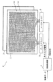
実施の形態1に係る液晶表示装置1を用いた画像表示装置2の概略構成について、図1〜図3を用いて説明する。図1は、実施の形態1に係る画像表示装置2の概略構成を模式的に示す図である。図2は、同画像表示装置2に用いられる液晶表示装置1の画素回路を示す図である。図3は、同液晶表示装置1における共通電極30の配置の一例を示す図である。なお、図2において、「G」はゲート線40を示し、「D」はデータ線50を示し、「T」はタッチ線60を示し、「VG」は、ゲート引出線41を示し、「dmyT」は、ダミータッチ線60Aを示し、「dmyVG」は、ダミーゲート引出線41Aを示している。また、図3において、黒丸は、各共通電極30とタッチ線60とのコンタクト部を示している。
(Embodiment 1)
The schematic configuration of the image display device 2 using the liquid
画像表示装置2は、静止画像又は動画像の画像(映像)を表示する表示装置の一例である。図1に示すように、画像表示装置2は、液晶表示装置1と、バックライト3と、画像処理部4とを備える。
The image display device 2 is an example of a display device that displays an image (video) of a still image or a moving image. As shown in FIG. 1, the image display device 2 includes a liquid
液晶表示装置1は、画像が表示される液晶表示パネルである。液晶表示装置1は、バックライト3の光出射側に配置される。したがって、液晶表示装置1には、バックライト3から出射した光が入射する。
The liquid
液晶表示装置1の液晶駆動方式は、例えばIPS(In−Plane Switching)方式及びFFS(Fringe Field Switching)方式等の横電界方式である。また、液晶表示装置1は、例えば、ノーマリーブラック方式により電圧の制御が行われるが、電圧制御の方式は、ノーマリーブラック方式に限らない。
The liquid crystal drive system of the liquid
図1及び図2に示すように、液晶表示装置1は、画像表示領域1a(アクティブ領域)と、画像表示領域1aを囲む額縁領域1bとを有する。画像表示領域1aには、カラー画像又はモノクロ画像が表示される。
As shown in FIGS. 1 and 2, the liquid
画像表示領域1aは、画像が表示される表示領域(有効領域)であり、例えば、第1方向と第1方向に交差する第2方向とに配列された複数の画素PXによって構成されている。本実施の形態において、第1方向と第2方向とは直交している。具体的には、第1方向は、行方向であり、第2方向は、行方向に直交する列方向である。したがって、画像表示領域1aは、行方向と列方向とに配列された複数の画素PXによって構成されている。つまり、複数の画素PXは、マトリクス状に配列されている。 The image display area 1a is a display area (effective area) in which an image is displayed, and is composed of, for example, a plurality of pixel PXs arranged in a first direction and a second direction intersecting the first direction. In the present embodiment, the first direction and the second direction are orthogonal to each other. Specifically, the first direction is the row direction, and the second direction is the column direction orthogonal to the row direction. Therefore, the image display area 1a is composed of a plurality of pixels PX arranged in the row direction and the column direction. That is, the plurality of pixels PX are arranged in a matrix.
額縁領域1bは、液晶表示装置1の周辺領域であって、画像表示領域1aの外側に位置する領域である。また、額縁領域1bは、画像が表示されない非表示領域(無効領域)である。本実施の形態において、液晶表示装置1の平面視形状は、矩形状である。したがって、画像表示領域1aの平面視形状は、矩形状であり、額縁領域1bの平面視形状は、矩形枠状である。
The
複数の画素PXは、行方向に沿って周期的に繰り返して配列された複数種の画素によって構成されている。具体的には、複数の画素PXは、赤色画素PXR、緑色画素PXG及び青色画素PXBの3種類の画素によって構成されている。この場合、本実施の形態では、赤色画素PXR、緑色画素PXG及び青色画素PXBの3つの画素がこの順で1組となって行方向に沿って繰り返して配列されている。なお、列方向には、同一種類の画素PXが配列されている。 The plurality of pixels PX are composed of a plurality of types of pixels arranged periodically and repeatedly along the row direction. Specifically, the plurality of pixels PX are composed of three types of pixels: a red pixel PXR, a green pixel PXG, and a blue pixel PXB. In this case, in the present embodiment, the three pixels of the red pixel PXR, the green pixel PXG, and the blue pixel PXB are arranged in this order as a set repeatedly along the row direction. The same type of pixels PX are arranged in the column direction.
図2に示すように、液晶表示装置1は、複数の画素PXの各々に設けられたトランジスタ10及び画素電極20と、画素電極20に対向する共通電極30とを備える。
As shown in FIG. 2, the liquid
また、液晶表示装置1は、第1方向である行方向に延在する複数のゲート線40(走査線)と、第1方向に直交する第2方向である列方向に延在する複数のデータ線50(映像信号線)とを備える。
Further, the liquid
液晶表示装置1は、さらに、ゲート線40に接続されたゲート引出線41と、ゲート線40に接続されていないダミーゲート引出線41Aとを備える。本実施の形態において、ゲート引出線41とダミーゲート引出線41Aとは、複数本ずつ設けられている。複数のゲート引出線41と複数のダミーゲート引出線41Aとは、複数のデータ線50と同じ方向に延在している。つまり、複数のゲート引出線41及び複数のダミーゲート引出線41Aは、タッチ線60と同様に、列方向に延在している。したがって、複数のゲート引出線41及び複数のダミーゲート引出線41Aは、複数のデータ線50と同じ方向に延在しているとともに、複数のゲート線40と直交している。
The liquid
また、本実施の形態における液晶表示装置1は、表示機能だけではなく、タッチ機能を有するインセル型の液晶表示パネル(インセルタッチパネル)である。したがって、液晶表示装置1は、さらに、ユーザが液晶表示装置1をタッチしたときのタッチ位置を検出するための複数のタッチ線60を備える。複数のタッチ線60は、複数のデータ線50と同じ方向に延在している。具体的には、複数のタッチ線60は、列方向に延在している。
Further, the liquid
さらに、本実施の形態における液晶表示装置1は、ユーザが液晶表示装置1をタッチしたときのタッチ位置を検出することに寄与しないダミータッチ線60Aを備える。本実施の形態において、ダミータッチ線60Aは、複数本設けられている。複数のダミータッチ線60Aは、複数のデータ線50と同じ方向に延在している。つまり、複数のダミータッチ線60Aは、タッチ線60と同様に、列方向に延在している。
Further, the liquid
各画素PXに設けられたトランジスタ10は、薄膜トランジスタ(TFT;Thin Film Transistor)であり、ゲート電極10G、ソース電極10S及びドレイン電極10Dを有する。なお、本明細書において、ソース電極10S及びドレイン電極10Dは、まとめてソースドレイン電極と記載することもあり、ソースドレイン電極とは、ソース電極10S及びドレイン電極10Dの少なくとも一方のこと、ソース電極10S及びドレイン電極10Dのいずれかのみのこと、あるいは、ソース電極10S及びドレイン電極10Dの両方のことを意味する。
The
画素電極20は、複数の画素PXの各々に設けられている。画素電極20は、複数の画素PXの各々において、当該画素PXに対応するトランジスタ10を介して当該画素PXに対応するゲート線40及びデータ線50と接続されている。
The
本実施の形態において、トランジスタ10及び画素電極20は、各画素PXに1つずつ設けられているが、トランジスタ10及び画素電極20は、各画素PXに複数ずつ設けられていてもよい。
In the present embodiment, one
各画素PXにおける画素電極20は、例えば、ストライプ状の複数本のライン電極を有する。一例として、画素電極20は、櫛歯状の電極又は複数のスリットが形成された電極である。なお、各画素電極20における複数本のライン電極は、列方向に隣り合う2つの画素PXで直線状のライン電極の向きを反転させて列方向の2画素分で略「く」の字状となるように形成されていてもよいし、1つの画素PX内で「く」の字状に屈曲されていてもよい。
The
共通電極30は、画素電極20に対向する対向電極である。図3に示すように、本実施の形態において、共通電極30は、複数設けられている。複数の共通電極30は、行方向及び列方向の各々に配列されている。つまり、複数の共通電極30は、マトリクス状に配列されている。複数の共通電極30の各々には、同一の共通電圧(Vcom)が印加される。
The
複数の共通電極30の各々は、矩形状であり、1つ以上の画素電極20に対向している。本実施の形態において、複数の共通電極30の各々は、複数の画素PXにわたって設けられた矩形状であり、矩形領域に存在する複数の画素PXに対応する複数の画素電極20に対向している。例えば、複数の共通電極30は、一辺が数十〜数十個の複数の画素PXからなる矩形状に形成されている。
Each of the plurality of
本実施の形態における液晶表示装置1は、自己容量方式の静電容量方式によるタッチセンシング機能を有する液晶表示パネルである。したがって、共通電極30は、画素電極20との間で容量を形成するタッチ電極でもある。つまり、共通電極30は、画素電極20と対になって、画像表示駆動の際に用いられるだけではなく、タッチ位置検出駆動の際にも用いられる。複数の共通電極30の各々は、タッチ位置を検出するための単位電極(タッチ電極)である。このように、タッチ位置検出駆動の際、共通電極30は、各々が1つ以上の画素電極20に対向するとともに互いに分離して設けられた複数のタッチ電極として構成される。
The liquid
複数の共通電極30は、マトリクス状に配列されており、行方向に延在する配線(ゲート線40)上と、列方向に延在する配線(データ線50、ゲート引出線41、ダミーゲート引出線41A、ダミータッチ線60A)上とを、分離領域として互いに分離されている。
The plurality of
1つの共通電極30のサイズは、例えば、40×40画素分である。つまり、1つの共通電極30の行方向及び列方向の長さが画素40個分の長さである。この場合、1つの共通電極30における1本のタッチ線60とのコンタクト部は、40ヵ所となる。なお、1つの共通電極30のサイズは、これに限るものではなく、32×32画素分であってもよし、また、正方形に限らず、長方形であってもよい。
The size of one
行方向に延在する複数のゲート線40の各々は、複数の画素PXの各々におけるトランジスタ10にゲート信号を供給する。複数のゲート線40の各々は、画像表示領域1a内において、列方向に隣り合う2つの画素PXの境界部に設けられている。具体的には、各ゲート線40は、列方向に隣り合う2の画素列の間に設けられている。複数のゲート線40は、例えば、直線状に行方向に延在している。
Each of the plurality of
各ゲート線40は、行方向に配列された複数の画素PXの各々のトランジスタ10と接続されている。つまり、各ゲート線40は、各画素PXにおいて、1つのトランジスタ10と接続されている。具体的には、各ゲート線40は、各トランジスタ10のゲート電極10Gと接続されている。
Each
本実施の形態において、液晶表示装置1は、デュアルゲート構造であり、2G1Dの配線接続構造を有している。したがって、複数のゲート線40は、列方向に隣り合う2つの画素PXの境界部ごとに2本ずつ設けられている。つまり、列方向に隣り合う2つの画素列の境界部ごとに、ゲート線40が2本ずつ設けられている。
In the present embodiment, the liquid
列方向に延在する複数のゲート引出線41及び列方向に延在する複数のダミーゲート引出線41Aの各々は、データ線50と同様に、画像表示領域1a内において、行方向に隣り合う2つの画素PXの境界部に設けられている。具体的には、各ゲート引出線41及び各ダミーゲート引出線41Aは、行方向に隣り合う2つの画素列の間に設けられている。複数のゲート引出線41及び複数のダミーゲート引出線41Aの各々は、例えば、直線状に行方向に延在しているが、画素毎に向きを反転させて列方向に沿ってジグサグ状となるように形成されていてもよい。
Each of the plurality of gate leader lines 41 extending in the column direction and the plurality of dummy
複数のゲート引出線41及び複数のダミーゲート引出線41Aは、複数のゲート線40と直交している。本実施の形態において、複数のゲート引出線41及び複数のダミーゲート引出線41Aは、データ線50と同層に形成されている。したがって、複数のゲート引出線41及び複数のダミーゲート引出線41Aと、複数のゲート線40とは、絶縁膜を介して立体交差している。
The plurality of gate leader lines 41 and the plurality of dummy
複数のゲート引出線41の各々は、ゲートドライバ5から出力されるゲート信号を、当該ゲート引出線41に対応するゲート線40に供給する。つまり、各ゲート引出線41は、中継配線として、ゲートドライバ5から出力されるゲート信号をゲート線40に供給するための中継配線である。したがって、複数のゲート引出線41は、複数のゲート線40と複数のゲート引出線41との複数の交差部のうちの少なくとも1箇所でゲート線40と接続されている。つまり、複数のゲート線40の各々は、1つ以上のゲート引出線41と電気的に接続されている。具体的には、複数のゲート線40と複数のゲート引出線41とは、画像表示領域1a内における複数のゲート線40と複数のゲート引出線41との複数の立体交差部のうちの少なくとも1箇所において、ゲートコンタクトホールを介して接続されている。
Each of the plurality of gate leader lines 41 supplies the gate signal output from the
例えば、1本のゲート線40と1本のゲート引出線41とは、1箇所で接続されている。したがって、各ゲート線40は、1箇所のゲートコンタクトホールにおいて1本のゲート引出線41に接続されている。なお、1本のゲート線40が2本以上の複数本のゲート引出線41に接続されていてもよい。この場合、1本のゲート線40は、複数箇所のゲートコンタクトホールにおいて複数本のゲート引出線41に接続される。
For example, one
このように、本実施の形態における液晶表示装置1では、ゲートドライバ5から出力されるゲート信号用の配線として、行方向に延在する横ゲート線であるゲート線40と列方向に延在する縦ゲート線であるゲート引出線41とが設けられている。
As described above, in the liquid
また、複数のダミーゲート引出線41Aの各々は、ゲート線40と立体交差しているが、ゲート線40には接続されていない。したがって、各ダミーゲート引出線41Aには、ゲート信号が供給されない。なお、ダミーゲート引出線41Aには、共通電圧(Vcom)等の所定の電圧が印加されていてもよいし、所定の電圧が印加されなくてもよい。つまり、ダミーゲート引出線41Aは、フローティングであってもよい。
Further, each of the plurality of dummy
列方向に延在する複数のデータ線50の各々は、複数の画素PXの各々におけるトランジスタ10にデータ信号(映像信号)を供給する。複数のデータ線50の各々は、画像表示領域1a内において、行方向に隣り合う2つの画素PXの境界部に設けられている。具体的には、各データ線50は、行方向に隣り合う2つの画素列の間に設けられている。本実施の形態において、複数のデータ線50と複数のゲート引出線41及び複数のダミーゲート引出線41Aとは、同層に形成されている。また、複数のデータ線50と複数のゲート引出線41とは、行方向に隣り合う2つの画素PXの境界部ごとに周期的に繰り返して設けられている。具体的には、複数のデータ線50と複数のゲート引出線41とは、行方向に隣り合う2つの画素PXの境界部ごとに1本ずつ交互に設けられている。つまり、複数のデータ線50と複数のゲート引出線41とは、列方向に並ぶ複数の画素PXからなる画素列ごとに1本ずつ交互に設けられている。例えば、データ線50とゲート引出線41とは、画素列の奇数ライン又は偶数ラインに分けて配置される。
Each of the plurality of
各データ線50は、列方向に配列された複数の画素PXの各々のトランジスタ10と接続されている。つまり、各データ線50は、各画素PXにおいて、1つのトランジスタ10と接続されている。具体的には、各データ線50は、各トランジスタ10のドレイン電極10Dと接続されている。つまり、本実施の形態において、データ線50は、ドレイン線である。なお、複数のデータ線50の各々は、例えば、直線状に行方向に延在しているが、画素毎に向きを反転させて列方向に沿ってジグサグ状となるように形成されていてもよい。
Each
列方向に延在する複数のタッチ線60の各々は、データ線50と同様に、画像表示領域1a内において、行方向に隣り合う2つの画素PXの境界部に設けられている。具体的には、タッチ線60は、行方向に隣り合う2つの画素列の間に設けられている。複数のタッチ線60の各々は、例えば、直線状に行方向に延在しているが、画素毎に向きを反転させて列方向に沿ってジグサグ状となるように形成されていてもよい。
Like the
図3に示すように、複数のタッチ線60は、複数の共通電極30のうち列方向に配列された複数の共通電極30と一対一で接続されている。具体的には、列方向に配列された複数の共通電極30の各列における複数のタッチ線60(列タッチ線群)の各々は、当該列に含まれる複数の共通電極30の全てを横断するように設けられているが、当該列に含まれる複数の共通電極30のいずれか1つのみに接続されている。したがって、各共通電極30は、当該共通電極30を横断する複数のタッチ線60のうちのいずれか1つと接続されているが、他の残りのタッチ線60とは接続されておらず絶縁されている。列方向に並ぶ共通電極30を跨るタッチ線60の本数は、列方向に並ぶ共通電極30と同数あればよい。
As shown in FIG. 3, the plurality of
タッチ線60と共通電極30とは絶縁膜を介して形成されており、タッチ線60と当該タッチ線60に対応する共通電極30とは絶縁膜に形成されたコンタクトホールを介して接続されている。このコンタクトホールは、タッチ線60と共通電極30とを接続するコンタクト部になる。
The
複数のタッチ線60は、複数のデータ線50、ゲート引出線41及びダミーゲート引出線41Aと同じ方向に延在しているが、複数のデータ線50、ゲート引出線41及びダミーゲート引出線41Aとは異なる層に設けられている。なお、複数のタッチ線60の各々は、平面視において、複数のデータ線50の各々に重なっているとよい。
The plurality of
列方向に延在する複数のダミータッチ線60Aの各々は、データ線50と同様に、画像表示領域1a内において、行方向に隣り合う2つの画素PXの境界部に設けられている。具体的には、ダミータッチ線60Aは、行方向に隣り合う2つの画素列の間に設けられている。本実施の形態において、ダミータッチ線60Aは、ダミーゲート引出線41Aが配置された画素列の間に設けられているが、これに限らない。また、ダミータッチ線60Aは、行方向に隣り合う2つの共通電極30を分離する分離領域(タッチ電極境界)に設けられている。複数のタッチ線60の各々は、例えば、直線状に行方向に延在しているが、画素毎に向きを反転させて列方向に沿ってジグサグ状となるように形成されていてもよい。
Like the
ダミータッチ線60Aは、タッチ線60とは異なり、タッチ位置を検出することに寄与しない。したがって、ダミータッチ線60Aは、共通電極30には接続されていない。具体的には、列方向に隣り合う2つの共通電極30の間に設けられるダミータッチ線60Aは、共通電極30と重なっていない。したがって、ダミータッチ線60Aと共通電極30とを接続するコンタクト部が形成されていない。
Unlike the
複数のダミータッチ線60Aは、複数のデータ線50、ゲート引出線41及びダミーゲート引出線41Aと同じ方向に延在しているが、複数のダミータッチ線60Aは、複数のデータ線50、ゲート引出線41及びダミーゲート引出線41Aとは異なる層に設けられている。本実施の形態において、ダミータッチ線60Aは、タッチ線60と同層に形成されている。
The plurality of
ダミータッチ線60Aは、ダミーゲート引出線41Aが配置された画素列間と同じ画素間に設けられている。この場合、複数のダミータッチ線60Aの各々は、平面視において、複数のダミーゲート引出線41Aの各々に重なっているとよい。
The
本実施の形態において、ダミータッチ線60Aは、画像表示領域1a内では、どの配線にも接続されていないが、額縁領域1bに引き出されて、ダミータッチ線60Aには、固定電圧が印加されている。具体的には、ダミータッチ線60Aと共通電極30とが同電位となるように、ダミータッチ線60Aには、共通電極30と同様に共通電圧(Vcom)が印加される。なお、ダミータッチ線60Aに印加される電圧は、共通電圧に限らず、ゲートオフ電圧(Vgoff)等の所定の電圧であってもよい。また、ダミータッチ線60Aには、所定の電圧が印加されなくてもよい。つまり、ダミータッチ線60Aは、フローティングであってもよい。
In the present embodiment, the
図1に示すように、液晶表示装置1は、入力された映像信号に応じた画像を表示するために、ゲートドライバ5及びソースドライバ6を有する。ゲートドライバ5及びソースドライバ6は、例えばドライバIC(ICパッケージ)である。
As shown in FIG. 1, the liquid
ゲートドライバ5及びソースドライバ6は、液晶表示装置1の額縁領域1bに実装される。具体的には、ゲートドライバ5及びソースドライバ6は、COF(Chip on Film)方式又はCOG(Chip on Glass)方式によって液晶表示装置1の端部に実装される。
The
ゲートドライバ5及びソースドライバ6をCOF方式によって実装する場合、FFC(Flexible Flat Cable)又はFPC(Flexible Printed Cable)等のフレキシブル配線基板にゲートドライバ5又はソースドライバ6が実装された異方性導電性フィルム(ACF;Anisotropic Conductive Film)からなるCOFを、熱圧着によって液晶表示装置1の端部に設けられた電極端子に接続する。
When the
一方、ゲートドライバ5及びソースドライバ6をCOG方式によって実装する場合、液晶表示装置1のアクティブマトリクス基板にゲートドライバ5及びソースドライバ6を直接実装する。
On the other hand, when the
なお、ゲートドライバ5及びソースドライバ6の両方をCOF方式又はCOG方式によって実装することに限らず、ゲートドライバ5及びソースドライバ6の一方をCOF方式で実装し、他方をCOG方式によって実装してもよい。
It should be noted that both the
図2に示すように、ゲートドライバ5は、ゲート線40に電気的に接続されている。本実施の形態において、ゲートドライバ5は、ゲート引出線41を介してゲート線40と電気的に接続されている。ゲートドライバ5は、画像処理部4から入力されるタイミング信号に応じてデータ信号を書き込む画素PXを選択し、選択した画素PXのトランジスタ10をオンする電圧(ゲートオン電圧;Vgon)をゲート線40に供給する。これにより、選択された画素PXの画素電極20には、トランジスタ10を介してデータ電圧が供給される。
As shown in FIG. 2, the
ソースドライバ6は、液晶表示装置1のデータ線50に接続されている。ソースドライバ6は、ゲートドライバ5によるゲート線40の選択に合わせて、画像処理部4から入力される映像信号に応じた電圧(データ電圧)をデータ線50に供給する。
The
本実施の形態では、ソースドライバ6として、タッチ機能付きソースドライバを用いている。タッチ機能付きソースドライバは、画像表示駆動を行う際に必要な画像表示回路とタッチ位置検出駆動を行う際に必要なタッチ位置検出回路とが共用化されたドライバである。本実施の形態において、複数のデータ線50と複数のタッチ線60とは、タッチ機能付きソースドライバであるソースドライバ6に接続されている。また、タッチ線60をコモン線として利用することで、タッチ機能付きソースドライバは、コモン線を介して共通電極30に共通電圧(Vcom)を供給する。
In this embodiment, a source driver with a touch function is used as the
ゲートドライバ5及びソースドライバ6は、額縁領域1bにおける一対の辺のうちの一方に実装されている。つまり、ゲートドライバ5及びソースドライバ6は、額縁領域1bの同じ辺に設けられている。
The
具体的には、ゲートドライバ5及びソースドライバ6は、液晶表示装置1の列方向側の端部に実装される。なお、ゲートドライバ5とソースドライバ6の実装箇所はこれに限るものではなく、ゲートドライバ5及びソースドライバ6が、額縁領域1bの異なる辺に実装されていてもよい。
Specifically, the
バックライト3は、図1に示すように、液晶表示装置1の背面側に配置されており、液晶表示装置1に向けて光を照射する。本実施の形態において、バックライト3は、LED(Light Emitting Diode)を光源とするLEDバックライトであるが、これに限るものではない。また、バックライト3は、液晶表示装置1に対面するようにLEDが基板上に二次元状に配列された直下型のLEDバックライトであるが、エッジ型のバックライトであってもよい。バックライト3は、平面状の均一な散乱光(拡散光)を照射する面発光ユニットである。なお、バックライト3は、光源からの光を拡散させるために拡散板(拡散シート)等の光学部材を有していてもよい。
As shown in FIG. 1, the
画像処理部4は、CPU等の演算処理回路と、ROMやRAM等のメモリとを備える制御装置である。画像処理部4には、液晶表示装置1に表示するための映像データが入力される。画像処理部4は、CPUがメモリに格納されたプログラムを読み出して実行することにより各種の処理を実行する。具体的には、画像処理部4は、外部のシステム(図示せず)から入力された映像データに対して色調整等の各種の画像信号処理を行って各画素PXの階調値を示す映像信号と、各画素PXに映像信号を書き込むタイミングを示すタイミング信号とを生成するタイミングコントローラ等を含む。画像処理部4は、映像信号をソースドライバ6に出力するとともにタイミング信号をゲートドライバ5に出力する。
The image processing unit 4 is a control device including an arithmetic processing circuit such as a CPU and a memory such as a ROM or RAM. Video data for display on the liquid
本実施の形態における液晶表示装置1は、表示機能及びタッチ機能を有する。つまり、液晶表示装置1は、画像表示駆動とタッチ位置検出駆動とを行う。この場合、液晶表示装置1では、タッチ線60を利用して、時分割によって画像表示駆動とタッチ位置検出駆動とを行う。例えば、図4A及び図4Bに示すように、1フレーム期間(16.6ms)内に画像表示駆動とタッチ位置検出駆動とを交互に複数回繰り返して行う。この場合、タッチ位置検出駆動は、例えばブランキング期間を利用して行うことができる。
The liquid
液晶表示装置1が画像表示駆動を行う際、ゲートドライバ5からのゲートオン電圧がゲート引出線41を介してゲート線40に供給される。これにより、選択された画素PXのトランジスタ10がオンし、このトランジスタ10に接続されたデータ線50からデータ電圧が画素電極20に供給される。そして、画素電極20に供給されたデータ電圧と共通電極30に供給された共通電圧との差により液晶層に電界が生じる。この電界により各画素PXにおける液晶層の液晶分子の配向状態が変化し、液晶表示装置1を通過するバックライト3の光の透過率が画素PXごとに制御される。これにより、液晶表示装置1の画像表示領域1aに所望の画像が表示される。
When the liquid
また、液晶表示装置1がタッチ位置検出駆動を行う際は、タッチ機能付きソースドライバであるソースドライバ6によって、タッチ線60を介して複数の共通電極30の各々の静電容量の変化をタッチ検出信号として検出する。これにより、タッチされた位置の共通電極30を特定することができ、ユーザがタッチした位置を検知することができる。
Further, when the liquid
なお、図4Bに示される制御は、図4Aに示される制御と比べて、画像表示駆動及びタッチ位置検出駆動の1回あたりの駆動期間が長い。本実施の形態では、図4Bに示される制御と図4Aに示される制御とのいずれを用いてもよい。ただし、図4Bに示される制御は、図4Aに示される制御と比べて、タッチ位置検出駆動中の画像データをメモリに蓄える量が多くなるため、ICドライバのチップサイズが大きくなる。 The control shown in FIG. 4B has a longer driving period per operation of the image display drive and the touch position detection drive than the control shown in FIG. 4A. In this embodiment, either the control shown in FIG. 4B or the control shown in FIG. 4A may be used. However, the control shown in FIG. 4B has a larger amount of image data stored in the memory during the touch position detection drive than the control shown in FIG. 4A, so that the chip size of the IC driver becomes larger.
次に、液晶表示装置1の断面構造の一例について、図5及び図6を用いて説明する。図5は、実施の形態1に係る液晶表示装置1の画素PXにおけるトランジスタ10の周辺の構成を示す断面図である。図6は、同液晶表示装置1におけるタッチ線60の周辺の構成を示す断面図である。
Next, an example of the cross-sectional structure of the liquid
図5に示すように、液晶表示装置1は、第1基板100と、第1基板100に対向する第2基板200と、第1基板100と第2基板200との間に配置された液晶層300とを備えている。本実施の形態では、第1基板100がバックライト3側に位置し、第2基板200が観察者側に位置する。なお、図示しないが、液晶層300は、枠状の封止部材によって第1基板100と第2基板200との間に封止されている。
As shown in FIG. 5, the liquid
第1基板100は、トランジスタ10としてTFTを有するTFT基板である。具体的には、第1基板100は、複数のトランジスタ10がマトリクス状に配列されたアクティブマトリクス基板である。また、第1基板100には、トランジスタ10だけではなく、ゲート線40、ゲート引出線41、ダミーゲート引出線41A、データ線50、タッチ線60及びダミータッチ線60A等の各種配線、これらの配線間を絶縁する絶縁膜、画素電極20及び共通電極30等が設けられている。これらの部材は、第1透明基材110の上に形成される。第1透明基材110は、例えば、ガラス基板等の透明基板である。
The
図5に示すように、第1透明基材110に形成されたトランジスタ10は、ゲート電極10Gと、ソース電極10Sと、ドレイン電極10Dと、チャネル層となる半導体層10SCとによって構成されている。本実施の形態において、トランジスタ10は、ボトムゲート構造のTFTであり、第1透明基材110の上に形成されたゲート電極10Gと、ゲート電極10Gの上に形成されたゲート絶縁膜(GI)である第1絶縁膜121と、第1絶縁膜121を介してゲート電極10Gの上方に形成された半導体層10SCとを備える。ソース電極10S及びドレイン電極10Dは、半導体層10SCの一部を覆うように形成されている。第1絶縁膜121は、ゲート電極10Gを覆うように第1透明基材110の全面にわたって形成されている。
As shown in FIG. 5, the
ゲート電極10Gは、例えば、モリブデン膜と銅膜との2層構造からなる金属膜によって構成されていてもよいし、銅膜等からなる1層の金属膜によって構成されていてもよい。第1絶縁膜121は、例えば、酸化シリコン膜と窒化シリコン膜との2層構造の絶縁膜によって構成されていてもよいし、酸化シリコン膜又は窒化シリコン膜の1層の絶縁膜によって構成されていてもよい。半導体層10SCは、例えば、i−アモルファスシリコン膜とn−アモルファスシリコン膜との2層構造からなる半導体膜によって構成されていてもよいし、i−アモルファスシリコン膜の1層のみの半導体膜によって構成されていてもよい。ソース電極10S及びドレイン電極10Dは、例えば、モリブデン膜と銅膜との2層構造からなる金属膜によって構成されていてもよいし、銅膜等からなる1層の金属膜によって構成されていてもよい。
The
なお、ゲート電極10G、ソース電極10S、ドレイン電極10D、半導体層10SC及び第1絶縁膜121の材料は、これらに限定されるものではない。例えば、半導体層10SCの材料としては、In−Ga−Zn−O系酸化物半導体等を用いてもよい。
The materials of the
図5に示すように、第1基板100には、ゲート線40及びデータ線50が形成されている。ゲート線40及びデータ線50は、第1透明基材110の上に形成される。
As shown in FIG. 5, a
ゲート線40は、ゲート電極10Gと同層に形成されている。つまり、ゲート線40とゲート電極10Gとは、同じ金属膜をパターニングすることによって形成される。ゲート線40とゲート電極10Gとは、メタル層である第1配線層(GAL層)に形成されている。
The
データ線50は、ソース電極10S及びドレイン電極10Dと同層に形成されている。つまり、データ線50とソース電極10S及びドレイン電極10Dとは、同じ金属膜をパターニングすることによって形成される。データ線50とソース電極10S及びドレイン電極10Dとは、第1配線層の上のメタル層である第2配線層(SD層)に形成されている。
The
なお、図示しないが、ゲート引出線41及びダミーゲート引出線41Aは、データ線50と同層に形成されている。つまり、ゲート引出線41及びダミーゲート引出線41Aは、SD層に形成されており、ゲート引出線41とダミーゲート引出線41Aとデータ線50とソース電極10S及びドレイン電極10Dとは、同じ金属膜をパターニングすることによって形成される。
Although not shown, the
第1配線層(GAL層)と第2配線層(SD層)との間には、第1絶縁層(GI層)として第1絶縁膜121が形成されている。第1絶縁膜121は、ゲート線40及びゲート電極10Gを覆うように第1透明基材110の全面にわたって形成されている。第1配線層、第1絶縁膜121及び第2配線層は、TFTであるトランジスタ10が形成されたTFT層である。
A first insulating
なお、トランジスタ10のソース電極10Sは、コンタクトホールを介して画素電極20に接続されている。一方、トランジスタ10のドレイン電極10Dは、データ線50に接続されている。具体的には、データ線50の一部がドレイン電極10Dとなっている。
The
また、第1絶縁膜121の上には、データ線50及びトランジスタ10のソースドレイン電極を覆うように、第2絶縁層(PAS層)として第2絶縁膜122が形成されている。つまり、データ線50及びトランジスタ10のソースドレイン電極は、第1絶縁膜121と第2絶縁膜122との間に形成されている。第2絶縁膜122は、第1絶縁膜121の全面にわたって形成されている。第2絶縁膜122は、例えば、窒化シリコン膜等の無機材料からなる無機絶縁膜によって構成されている。無機絶縁膜である第2絶縁膜122は、例えばCVD(Chemical Vapor Deposition)法によって成膜することができる。
Further, on the first insulating
さらに、第2絶縁膜122の上には、第3絶縁層(OPAS層)として第3絶縁膜123が形成されている。第3絶縁膜123は、第2絶縁膜122の全面にわたって形成されている。本実施の形態において、第3絶縁膜123の厚さは、第2絶縁膜122の厚さよりも厚い。具体的には、第3絶縁膜123の厚さは、第2絶縁膜122の厚さの10倍以上であり、一例として、3000nmである。これにより、ゲート線40及びデータ線50等の配線と共通電極30との間の厚み方向の距離を大きくすることができるので、ゲート線40及びデータ線50等の配線と共通電極30とで形成される寄生容量を軽減することができる。しかも、第3絶縁膜123を厚くすることで、トランジスタ10、ゲート線40及びデータ線50を形成することで生じるTFT層の凹凸差を軽減してTFT層を平坦化することもできる。これにより、表面が平坦化された第3絶縁膜123を形成することができるので、第3絶縁膜123の直上の共通電極30を平坦な平面状に形成することができる。つまり、第3絶縁膜123は、平坦化層として機能している。
Further, a third
また、第3絶縁膜123は、炭素を含む有機材料からなる有機絶縁膜によって構成されている。有機絶縁膜である第3絶縁膜123は、例えば液状の有機材料を塗布して硬化することによって形成することができる。これにより、第3絶縁膜123を容易に厚膜化することができるので、全ての画素PXにわたって第3絶縁膜123の表面を容易に平坦にすることができる。
Further, the third
第3絶縁膜123の上には、タッチ線60が形成されている。図示しないが、タッチ線60と同層に形成されるダミータッチ線60Aも、第3絶縁膜123の上に形成される。タッチ線60及びダミータッチ線60Aは、金属等の低抵抗材料によって構成されている。例えば、タッチ線60及びダミータッチ線60Aは、銅等によって構成された金属膜である。本実施の形態において、タッチ線60及びダミータッチ線60Aは、銅膜からなる銅線である。タッチ線60及びダミータッチ線60Aは、第2配線層の上のメタル層である第3配線層(CMT層)に形成されている。したがって、タッチ線60及びダミータッチ線60Aは、ゲート線40及びデータ線50とは異なる層に設けられている。
A
第3絶縁膜123とタッチ線60の上には、第4絶縁層(TPS層)として第4絶縁膜124が形成されている。なお、第3絶縁膜123は、タッチ線60と同層に形成されるダミータッチ線60Aも覆っている。したがって、タッチ線60及びダミータッチ線60Aは、第3絶縁膜123と第4絶縁膜124との間に形成されている。第4絶縁膜124は、タッチ線60及びダミータッチ線60Aを覆うように第3絶縁膜123の全面にわたって形成されている。第4絶縁膜124は、例えば、窒化シリコン膜等の無機材料からなる無機絶縁膜によって構成されている。
A fourth insulating
第4絶縁膜124の上には、共通電極30が形成されている。共通電極30は、例えば、インジウム錫酸化物(ITO:Indium Tin Oxide)等の透明金属酸化物によって構成された透明電極である。本実施の形態において、共通電極30は、ITO膜である。共通電極30は、第3配線層の上の第4配線層(MIT層)に形成されている。
A
上述のように、共通電極30は複数形成されている。具体的には、図3に示すように、共通電極30は、行方向及び列方向に互いに分離した状態でマトリクス状に配置されている。
As described above, a plurality of
また、複数の共通電極30は、画像表示領域1a内の全ての画素PXにわたって形成されている。これにより、ゲート線40及びデータ線50等の配線が共通電極30によって覆われるので、ゲート線40及びデータ線50等の配線で発生する電界を共通電極30によって遮蔽することができる。つまり、TFT層で発生する電界を共通電極30によってシールドすることができる。したがって、共通電極30の上に形成される画素電極20の形状及び大きさの設計の自由度が向上するので、画素PXの光透過率及び開口率を容易に向上させることができる。
Further, the plurality of
図6に示すように、共通電極30は、第4絶縁膜124に形成されたコンタクトホール124aを介して1本のタッチ線60に接続されている。これにより、タッチ位置検出駆動を行う際に、ユーザがタッチした位置の共通電極30の容量変化を、当該共通電極30に接続されたタッチ線60を介して検出することができる。
As shown in FIG. 6, the
また、ITO膜は比較的に抵抗値が高いが、このように低抵抗の金属膜からなるタッチ線60を共通電極30に接続することによって、ITO膜からなる共通電極30を低抵抗化することができ、共通電極30の時定数を下げることができる。つまり、画像表示駆動を行う際に、タッチ線60をコモン線として利用することができる。
Further, although the ITO film has a relatively high resistance value, the resistance of the
さらに、タッチ線60の上に共通電極30を設けることで、共通電極30によってタッチ線60を覆うことができる。これにより、共通電極30上にタッチ線60を設ける場合と比べて、腐食しやすい金属材料からなるタッチ線60の腐食を抑制することができる。
Further, by providing the
第4絶縁膜124及び共通電極30の上には、第5絶縁層(UPS層)として第5絶縁膜125が形成されている。第5絶縁膜125は、共通電極30を覆うように第4絶縁膜124の全面にわたって形成されている。第5絶縁膜125は、例えば、窒化シリコン膜等の無機材料からなる無機絶縁膜によって構成されている。
A fifth insulating
第5絶縁膜125の上には、画素電極20が形成されている。画素電極20は、第5絶縁膜125を介して共通電極30に対向している。画素電極20は、例えば、インジウム錫酸化物等の透明金属酸化物によって構成された透明電極である。本実施の形態において、画素電極20は、共通電極30と同様に、ITO膜である。画素電極20は、第4配線層の上の第5配線層(PIT層)に形成されている。
A
なお、図示しないが、画素電極20を覆うように第5絶縁膜125の全面にわたって配向膜が形成されていてもよい。液晶分子の初期配向角度を一定方向に揃えるために、配向膜にはラビング処理が施されている。
Although not shown, an alignment film may be formed over the entire surface of the fifth insulating
次に、第2基板200について説明する。第2基板200は、第1基板100に対向する対向基板である。図5及び図6に示すように、第2基板200は、第2透明基材210と、第2透明基材210に形成されたブラックマトリクス220と、カラーフィルタ230とを有する。したがって、第2基板200は、カラーフィルタ230を有するカラーフィルタ基板(CF基板)となる。
Next, the
第2透明基材210は、第1透明基材110と同様に、例えば、ガラス基板等の透明基板である。
The second
ブラックマトリクス220は、黒色層の遮光層であり、例えばカーボンブラックによって構成されている。ブラックマトリクス220は、第2透明基材210の液晶層300側の面に形成される。ブラックマトリクス220は、行方向及び列方向に隣り合う2つの画素間に形成される。したがった、ブラックマトリクス220は、画素間に配置された各種配線を覆うように形成されている。一例として、ブラックマトリクス220は、全体として格子状に形成される。
The
カラーフィルタ230は、複数の画素PXごとに形成されている。具体的には、カラーフィルタ230は、赤色画素PXR、緑色画素PXG及び青色画素PXBの各々に対応して、赤色カラーフィルタ、青色カラーフィルタ及び緑色カラーフィルタが形成される。各カラーフィルタは、ブラックマトリクス220の間の領域(つまりブラックマトリクス220の開口部)に形成される。
The
また、第2基板200は、複数のスペーサ240を有する。スペーサ240は、第1基板100に向かって突出するように第2透明基材210に形成されている。スペーサ240は、第1基板100と第2基板200との間隔(セルギャップ)を一定に維持するための柱状部材である。スペーサ240を設けることで、液晶層300の厚さを容易に一定に維持することができる。一例として、スペーサ240は、円柱台形状であり、上端部及び下端部の平面視形状は円形である。スペーサ240は、アクリル樹脂等の樹脂材料によって構成されており、弾性変形することができる。スペーサ240は、例えばフォトリソグラフィー等によって所定のパターンに形成することができる。
Further, the
なお、液晶表示装置1には、一対の偏光板(不図示)が貼り合わされている。例えば、一対の偏光板の一方が第1基板100の外面に形成され、一対の偏光板の他方が第2基板200の外面に形成される。一対の偏光板は、偏光方向が互いに直交するように配置されている。また、一対の偏光板には、位相差板が貼り合わされていてもよい。
A pair of polarizing plates (not shown) are attached to the liquid
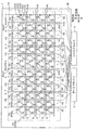
次に、図7〜図10を用いて、実施の形態1に係る液晶表示装置1の効果等について、本開示に至った経緯も含めて説明する。図7〜図10は、それぞれ、実施の形態1に係る液晶表示装置1の一態様における画素配列と配線との関係を示す図である。このうち、図10は、図1〜図6に示される液晶表示装置1そのものにおける画素配列と配線との関係を示している。なお、図7〜図10において、「D」に対応する太い実線は、データ線50を示しており、「VG」に対応する一点鎖線は、ゲート引出線41を示しており、「T」に対応する細い実線は、タッチ線60を示しており、「dmyVG」に対応する太い破線は、ダミーゲート引出線41Aを示しており、「dmyT」に対応する細い破線は、ダミータッチ線60Aを示しており、「G」に対応する実線は、ゲート線40を示している。また、「R」、「G」及び「B」で示される領域は、それぞれ、赤色画素PXRの画素列、緑色画素PXGの画素列及び青色画素PXBの画素列を示している。
Next, with reference to FIGS. 7 to 10, the effects and the like of the liquid
液晶表示装置では、狭額縁化等を目的として、ゲートドライバとソースドライバとを額縁領域の同じ辺に設ける技術が提案されている。例えば、ゲートドライバとソースドライバとを、額縁領域における画素の列方向の端部に設けることが考えられる。この場合、行方向に延在するゲート線と列方向の端部に実装されたゲートドライバとを電気的に接続するために、中継配線として列方向に延在するゲート引出線を別途形成することが考えられる。具体的には、ゲート線に直交するように複数のゲート引出線を形成し、ゲート引出線とゲート線との交差部でゲート引出線とゲート線とを接続することで、ゲート線とゲートドライバとをゲート引出線を介して接続する。 In the liquid crystal display device, a technique has been proposed in which a gate driver and a source driver are provided on the same side of the frame area for the purpose of narrowing the frame. For example, it is conceivable to provide a gate driver and a source driver at the end of the pixel in the frame area in the column direction. In this case, in order to electrically connect the gate wire extending in the row direction and the gate driver mounted at the end in the column direction, a gate leader wire extending in the column direction is separately formed as a relay wiring. Can be considered. Specifically, by forming a plurality of gate leader lines so as to be orthogonal to the gate line and connecting the gate leader line and the gate line at the intersection of the gate leader line and the gate line, the gate line and the gate driver And are connected via a gate leader.
このように構成すると、ゲート引出線とデータ線とが同じ方向に延在することになるので、製造工程でのマスク数の増加を抑えるために、ゲート引出線とデータ線とを同層に形成することが考えられる。つまり、ゲート引出線とデータ線とを同じ工程でパターニングすることが考えられる。 With this configuration, the gate leader line and the data line extend in the same direction, so the gate leader line and the data line are formed in the same layer in order to suppress an increase in the number of masks in the manufacturing process. It is conceivable to do. That is, it is conceivable to pattern the gate leader line and the data line in the same process.
しかしながら、ゲート引出線とデータ線とを同じ方向に延在させるとともにゲート引出線とデータ線とを同層に形成すると、データ線が配置された画素間にゲート引出線までも配置されてしまう。この結果、1つの画素間にゲート引出線とデータ線との2本の配線が並ぶことになる。この結果、画素の開口率や透過率が低下し、画像品位が低下する。 However, if the gate leader line and the data line extend in the same direction and the gate leader line and the data line are formed in the same layer, even the gate leader line is arranged between the pixels in which the data line is arranged. As a result, two wires, a gate leader line and a data line, are lined up between one pixel. As a result, the aperture ratio and transmittance of the pixels are lowered, and the image quality is lowered.
そこで、本願発明者らは、この課題を解決するために鋭意検討した。その結果、ゲート引出線とデータ線とのレイアウトを工夫することで、ゲート引出線とデータ線とが同じ方向に延在し且つ同層に形成されていたとしても画素の開口率や透過率が低下することを抑制できることを見出した。 Therefore, the inventors of the present application have diligently studied to solve this problem. As a result, by devising the layout of the gate leader line and the data line, even if the gate leader line and the data line extend in the same direction and are formed in the same layer, the aperture ratio and transmittance of the pixels can be increased. It was found that the decrease can be suppressed.
具体的には、まず、デュアルゲート構造を採用してゲート引出線とデータ線とを配置した。デュアルゲート構造では、図7に示すように、ゲート線40は、列方向に隣り合う2つの画素の境界部ごとに2本ずつ配置されるとともに、データ線50は、行方向の2つの画素ごとに設けられる。つまり、データ線50については、画素間を一つ飛ばしにして配置される。例えば、画素列の奇数ラインのみ又は偶数ラインのみにデータ線50を配置する。
Specifically, first, a dual gate structure was adopted and the gate leader line and the data line were arranged. In the dual gate structure, as shown in FIG. 7, two
このように、デュアルゲート構造を採用することで、隣り合う2本のデータ線50の間に、データ線50が形成されない画素の境界部が存在することになるので、この空いた画素の境界部を利用して、データ線50と同層にゲート引出線41を形成することができる。つまり、図7に示すように、データ線50とゲート引出線41とは、行方向に隣り合う2つの画素の境界部ごとに1本ずつ交互に設けられる。例えば、データ線50を画素列の奇数ラインに配置した場合、ゲート引出線41を偶数ラインに配置する。あるいは、データ線50を画素列の偶数ラインに配置した場合、ゲート引出線41を奇数ラインに配置する。
In this way, by adopting the dual gate structure, the boundary portion of the pixel in which the
このように、図7に示される液晶表示装置の構成によれば、複数のデータ線50と複数のゲート引出線41とは、同層に形成されており、かつ、行方向に隣り合う2つの画素の境界部ごとに周期的に繰り返して設けられている。これにより、平面視で1つの画素列間に2本の配線を並んで配置する必要がなくなる。
As described above, according to the configuration of the liquid crystal display device shown in FIG. 7, the plurality of
これにより、ゲート線40に交差するゲート引出線41とデータ線50とが同じ方向に延在し且つ同層に形成されていたとしても、画素PXの開口率や透過率が低下することを抑制できる。したがって、開口率や透過率の低下に伴って画像品位が低下することを抑制できる。
As a result, even if the
また、近年、タッチ機能を有するインセル方式の液晶表示装置が検討されている。この種の液晶表示装置では、ユーザがタッチした位置を検出するために、複数の共通電極に接続されたタッチ線を形成する。この場合、タッチ線とデータ線とを同じ方向に沿って形成して、タッチ機能付きソースドライバに接続することが考えられる。例えば、データ線とタッチ線とをいずれも列方向に延在するように形成することが考えられる。この場合、列方向に延在する配線として、データ線とゲート引出線とに加えて、タッチ線も形成されることになる。 Further, in recent years, an in-cell liquid crystal display device having a touch function has been studied. In this type of liquid crystal display device, a touch line connected to a plurality of common electrodes is formed in order to detect a position touched by the user. In this case, it is conceivable that the touch line and the data line are formed along the same direction and connected to the source driver with a touch function. For example, it is conceivable to form both the data line and the touch line so as to extend in the column direction. In this case, a touch line is formed in addition to the data line and the gate leader line as the wiring extending in the column direction.
例えば、図7に示される構成の液晶表示装置に、列方向に延在するタッチ線60を配置すると、図8に示される構成の液晶表示装置が考えられる。具体的には、図8に示すように、緑色画素PXGと青色画素PXBとの間のみにタッチ線60を配置することが考えられる。この場合、タッチ線60は、平面視においてデータ線50とゲート引出線41との各々に重なるように、データ線50が配置された画素間とゲート引出線41が配置された画素間とに交互に配置される。
For example, when the
このため、図8に示される構成の液晶表示装置では、ゲート引出線41の容量に周期性が生じるため、表示ムラが発生するおそれがある。特に、ゲート線40に接続されるゲート引出線41にはパルス状のゲート電圧が印加されるため、ゲート引出線41の容量による表示ムラへの感度が高い。また、タッチ線60の容量の周期性によってタッチ位置の検出性能が低下するおそれもある。さらに、ゲート引出線41にはパルス状のゲート電圧が印加されるため、ゲート引出線41とタッチ線60との結合容量に起因して表示ムラが発生するおそれもある。
Therefore, in the liquid crystal display device having the configuration shown in FIG. 8, the capacitance of the
そこで、図9に示される構成の液晶表示装置が考えられる。具体的には、図9に示すように、タッチ線60をデータ線50上のみに配置し、ゲート引出線41の上にはタッチ線60を配置しないようにする。
Therefore, a liquid crystal display device having the configuration shown in FIG. 9 can be considered. Specifically, as shown in FIG. 9, the
しかしながら、図9に示される構成の液晶表示装置では、隣り合う2つの画素の種類が同じ組み合わせの画素間に、タッチ線60が配置されるタッチ線配置画素間と、タッチ線60が配置されないタッチ線非配置画素間とが存在することになり、タッチ線配置画素間とタッチ線非配置画素間とが周期的に繰り返すことになる。例えば、図9では、緑色画素PXGと青色画素PXBとの画素間については、タッチ線60が配置されるタッチ線配置画素間とタッチ線60が配置されないタッチ線非配置画素間とが1画素おきに繰り返して存在している。
However, in the liquid crystal display device having the configuration shown in FIG. 9, the
これにより、図9に示される構成の液晶表示装置では、タッチ線配置画素間とタッチ線非配置画素間とが周期的に繰り返して存在するので、幾何光学的ムラが発生して画像品位が低下するおそれがある。 As a result, in the liquid crystal display device having the configuration shown in FIG. 9, since the touch line-arranged pixels and the touch-line-non-arranged pixels are periodically and repeatedly present, geometrical optics unevenness occurs and the image quality is deteriorated. There is a risk of
そこで、図10に示される構成の液晶表示装置1が考えられる。図10に示される液晶表示装置1は、図8に示される液晶表示装置において、タッチ線60とゲート引出線41とが重なる画素間について、タッチ線60及びゲート引出線41をダミータッチ線60A及びダミーゲート引出線41Aに代えた構成になっている。
Therefore, the liquid
この場合、行方向に隣り合う2つの画素PXの境界部は、データ線50が配置される第1境界部と、ゲート引出線41又はダミーゲート引出線41Aが配置される第2境界部とを交互に含んでおり、タッチ線60は、第1境界部に配置され、ダミータッチ線60Aは、第2境界部に配置されている。
In this case, the boundary between the two pixels PX adjacent to each other in the row direction includes a first boundary where the
この構成により、図8に示される構成の液晶表示装置の課題と図9に示される液晶表示装置の課題とを解決することができる。 With this configuration, it is possible to solve the problems of the liquid crystal display device having the configuration shown in FIG. 8 and the problems of the liquid crystal display device shown in FIG.
つまり、図10に示される液晶表示装置では、ゲート引出線41の容量を共通にすることができるので、ゲート引出線41の容量の周期性に起因する表示ムラを抑制できる。また、タッチ線60の容量を共通にすることができるので、タッチ線の容量の周期性に起因するタッチ位置の検出性能の低下を抑制できる。さらに、ゲート引出線41とタッチ線60とが重ならないので、ゲート引出線41とタッチ線60との結合容量に起因する表示ムラの発生も抑制できる。
That is, in the liquid crystal display device shown in FIG. 10, since the capacity of the
また、図10に示される液晶表示装置1では、隣り合う2つの画素の種類が同じ組み合わせの画素間については、タッチ線60又はタッチ線60と同一視されるダミータッチ線60Aが配置されることになる。例えば、図10では、緑色画素PXGと青色画素PXBとの画素間については、タッチ線60が配置される画素間とダミータッチ線60Aが配置されない画素間とが1画素おきに繰り返している。これにより、タッチ線60の配置/非配置による幾何光学的ムラを抑制できる。
Further, in the liquid
特に、本実施の形態では、タッチ線60又はダミータッチ線60Aが、緑色画素PXG及び青色画素PXBとの間(GB間)のみに設けられており、赤色画素PXRと緑色画素PXGとの間(RG間)及び赤色画素PXRと青色画素PXBとの間(RB間)には設けられていない。これにより、赤色の単色ラスター表示のときの色ムラを効果的に抑制することができ、上記実施の形態1と比べて、レンズムラの対策も可能となる。なお、レンズムラとは、例えば特開2017−167351号公報に記載のように、タッチ線60又はダミータッチ線60Aで反射したバックライトからの光が、データ線50等の他の配線で再度反射して観察者側に透過した際に、タッチ線60の波長反射特性に依存して色ムラがみえてしまう現状をいう。例えば、タッチ線60が主として銅にて構成される場合、タッチ線60は赤成分の光を多く反射するため、タッチ線60で反射したバックライトからの光が、データ線等の他の配線で再度反射し赤画素から観察者側に抜け出て色ムラを引き起こす。
In particular, in the present embodiment, the
このように、図10に示される液晶表示装置1によれば、デュアルゲート構造を採用してゲート線40に交差するゲート引出線41とデータ線50とを同じ方向に延在させ且つ同層に形成し、しかも、タッチ機能を持たせるためにタッチ線60を配置したとしても、画像品位が低下することを効果的に抑制することができる。
As described above, according to the liquid
(実施の形態2)
次に、実施の形態2に係る液晶表示装置について、図11を用いて説明する。図11は、実施の形態2に係る液晶表示装置における画素配列と配線との関係を示す図である。
(Embodiment 2)
Next, the liquid crystal display device according to the second embodiment will be described with reference to FIG. FIG. 11 is a diagram showing the relationship between the pixel arrangement and the wiring in the liquid crystal display device according to the second embodiment.
本実施の形態に係る液晶表示装置は、上記実施の形態1に係る液晶表示装置1と同様に、複数の画素PXの各々に設けられたトランジスタ10及び画素電極20と、行方向及び列方向に配列された複数の共通電極30と、行方向に延在する複数のゲート線40と、列方向に延在する複数のゲート引出線41と、列方向に延在する複数のデータ線50と、列行方向に延在する複数のタッチ線60とを備える。
The liquid crystal display device according to the present embodiment is the same as the liquid
また、本実施の形態における液晶表示装置でもデュアルゲート構造が採用されており、複数のゲート線40は、列方向に隣り合う2つの画素PXの境界部ごとに2本ずつ設けられている。
Further, the liquid crystal display device according to the present embodiment also adopts a dual gate structure, and a plurality of
ただし、本実施の形態における液晶表示装置では、上記実施の形態における液晶表示装置1とは異なり、ダミーゲート引出線41A及びダミータッチ線60Aが設けられていない。
However, unlike the liquid
また、本実施の形態における液晶表示装置では、上記実施の形態1における液晶表示装置1と同様に、複数の画素PXは、赤色画素PXR、緑色画素PXG及び青色画素PXBの3種類の画素によって構成されている。そして、本実施の形態における液晶表示装置でも、上記実施の形態1における液晶表示装置1と同様に、複数の画素PXは、行方向に沿って周期的に繰り返して配列された複数種の画素によって構成されている。
Further, in the liquid crystal display device according to the present embodiment, similarly to the liquid
ただし、上記実施の形態における液晶表示装置1とは異なり、3種類の画素の配列が異なる。具体的には、本実施の形態における液晶表示装置では、図11に示すように、赤色画素PXR、緑色画素PXG、青色画素PXB、緑色画素PXG、青色画素PXB及び赤色画素PXRの6つの画素がこの順で1組となって行方向に沿って繰り返して配列されている。つまり、上記実施の形態1では、赤色画素PXR、緑色画素PXG及び青色画素PXBの3種類の画素PXが、RGBRGBの配列を1周期として配置されていたが、本実施の形態では、RGBGBRの配列を1周期として画素PXが配置されている。図11では、RGBGBRを1周期として2周期分が図示されている。なお、列方向には、同一種類の画素PXが配列されている。
However, unlike the liquid
また、本実施の形態における液晶表示装置では、上記実施の形態1における液晶表示装置1と同様に、複数のデータ線50と複数のゲート引出線41とは、同層に形成されており、かつ、行方向に隣り合う2つの画素PXの境界部ごとに周期的に繰り返して設けられている。また、本実施の形態における液晶表示装置でも、平面視において、複数のタッチ線60の各々は、複数のデータ線50の各々に重なっている。
Further, in the liquid crystal display device of the present embodiment, similarly to the liquid
ただし、本実施の形態における液晶表示装置では、ダミーゲート引出線41A及びダミータッチ線60Aが設けられていないので、上記実施の形態1における液晶表示装置1とは、列方向に延在する配線(データ線50.ゲート引出線41、タッチ線60)の繰り返しのレイアウトが異なる。
However, since the liquid crystal display device according to the present embodiment is not provided with the dummy
つまり、上記実施の形態1では、画素PXの配列をRGBRGBの配列に維持する代わりに、ダミーゲート引出線41A及びダミータッチ線60Aを別途設けたが、本実施の形態では、ダミーゲート引出線41A及びダミータッチ線60Aを別途設けない代わりに、画素PXの配列をRGBGBRの配列に変更している。
That is, in the first embodiment, instead of maintaining the arrangement of the pixel PX in the array of RGBRGB, the dummy
このように構成される本実施の形態に係る液晶表示装置でも、上記実施の形態1における液晶表示装置と同様の効果を得ることができる。 The liquid crystal display device according to the present embodiment configured as described above can also obtain the same effect as the liquid crystal display device according to the first embodiment.
すなわち、本実施の形態に係る液晶表示装置でも、図7に示される構成の配線レイアウトを含むので、ゲート線40に交差するゲート引出線41とデータ線50とが同じ方向に延在し且つ同層に形成されていたとしても、画素PXの開口率や透過率が低下することを抑制することができる。したがって、画像品位が低下することを抑制できる。
That is, since the liquid crystal display device according to the present embodiment also includes the wiring layout having the configuration shown in FIG. 7, the
さらに、本実施の形態に係る液晶表示装置でも、図8に示される構成の液晶表示装置の課題と図9に示される液晶表示装置の課題とを解決することができる。 Further, the liquid crystal display device according to the present embodiment can also solve the problems of the liquid crystal display device having the configuration shown in FIG. 8 and the problems of the liquid crystal display device shown in FIG.
具体的には、本実施の形態に係る液晶表示装置でも、ゲート引出線41の容量を共通にすることができるので、ゲート引出線41の容量の周期性に起因する表示ムラを抑制できる。また、タッチ線60の容量を共通にすることができるので、タッチ線の容量の周期性に起因するタッチ位置の検出性能の低下を抑制できる。さらに、ゲート引出線41とタッチ線60とが重ならないので、ゲート引出線41とタッチ線60との結合容量に起因する表示ムラも発生しない。また、本実施の形態に係る液晶表示装置でも、タッチ線60の配置/非配置による幾何光学的ムラを抑制できる。
Specifically, even in the liquid crystal display device according to the present embodiment, since the capacity of the
このように、本実施の形態に係る液晶表示装置についても、デュアルゲート構造を採用してゲート線40に交差するゲート引出線41とデータ線50とが同じ方向に延在し且つ同層に形成され、しかも、タッチ機能を持たせるためにタッチ線60を配置したとしても、画像品位が低下することを効果的に抑制することができる。
As described above, also in the liquid crystal display device according to the present embodiment, the dual gate structure is adopted, and the
また、本実施の形態における液晶表示装置は、上記実施の形態1における液晶表示装置と比べて、さらに、以下の効果も奏する。 Further, the liquid crystal display device according to the present embodiment also has the following effects as compared with the liquid crystal display device according to the first embodiment.
具体的には、データ線50の容量も共通にすることができるので、データ線50の容量の周期性に起因する表示ムラも抑制できる。
Specifically, since the capacity of the
また、ダミーゲート引出線41A及びダミータッチ線60Aを設ける必要がないので、データ線50を配置できる有効領域を多くできるので、液晶表示装置の行方向の長さが無駄に大きくなることを抑制できる。これにより、縦長(Landscape型)の画像表示領域1aを有する液晶表示装置を容易に実現することができる。例えば、縦横比(アスペクト比)が3:2の画像表示領域1aを実現できる。
Further, since it is not necessary to provide the dummy
さらに、ダミーゲート引出線41A及びダミータッチ線60Aを設けないことで、ダミーゲート引出線41A及びダミータッチ線60Aを設ける場合と比べて、額縁領域1bの周辺に形成される斜め配線による抵抗成分を小さくすることができる。つまり、ゲートドライバ5に接続するためにゲート引出線41を額縁領域1bに集約させたり、ソースドライバ6に接続するためにデータ線50及びタッチ線60を額縁領域1bに集約させたりすると、額縁領域1bの周辺には、これらの配線を引き回すために中継配線として斜め配線が形成されるが、ダミーゲート引出線41A及びダミータッチ線60Aを設けないことで、この斜め配線の領域を小さくすることができる。これにより、斜め配線の線路長による抵抗成分を小さくすることができる。
Further, by not providing the dummy
(実施の形態3)
次に、実施の形態3に係る液晶表示装置について、図12を用いて説明する。図12は、実施の形態3に係る液晶表示装置における画素配列と配線との関係を示す図である。
(Embodiment 3)
Next, the liquid crystal display device according to the third embodiment will be described with reference to FIG. FIG. 12 is a diagram showing the relationship between the pixel arrangement and the wiring in the liquid crystal display device according to the third embodiment.
本実施の形態に係る液晶表示装置は、上記実施の形態1に係る液晶表示装置1と同様に、複数の画素PXの各々に設けられたトランジスタ10及び画素電極20と、行方向及び列方向に配列された複数の共通電極30と、行方向に延在する複数のゲート線40と、列方向に延在する複数のゲート引出線41と、列方向に延在する複数のデータ線50と、列行方向に延在する複数のタッチ線60とを備える。
The liquid crystal display device according to the present embodiment is the same as the liquid
また、本実施の形態における液晶表示装置でもデュアルゲート構造が採用されており、複数のゲート線40は、列方向に隣り合う2つの画素PXの境界部ごとに2本ずつ設けられている。
Further, the liquid crystal display device according to the present embodiment also adopts a dual gate structure, and a plurality of
ただし、本実施の形態における液晶表示装置では、上記実施の形態における液晶表示装置1とは異なり、ダミーゲート引出線41A及びダミータッチ線60Aが設けられていない。
However, unlike the liquid
また、本実施の形態における液晶表示装置では、上記実施の形態1における液晶表示装置1と同様に、複数の画素PXは、赤色画素PXR、緑色画素PXG及び青色画素PXBの3種類の画素によって構成されている。そして、本実施の形態における液晶表示装置でも、上記実施の形態1における液晶表示装置1と同様に、赤色画素PXR、緑色画素PXG及び青色画素PXBの3つの画素がこの順で1組となって行方向に沿って繰り返して配列されている。具体的には、本実施の形態における液晶表示装置でも、RGBRGBの配列を1周期として画素PXが配置されている。なお、列方向には、同一種類の画素PXが配列されている。
Further, in the liquid crystal display device according to the present embodiment, similarly to the liquid
また、本実施の形態における液晶表示装置では、上記実施の形態1における液晶表示装置1と同様に、複数のデータ線50と複数のゲート引出線41とは、同層に形成されている。さらに、本実施の形態における液晶表示装置では、データ線50及びゲート引出線41だけではなく、タッチ線60も同層に形成されている。つまり、複数のデータ線50、複数のゲート引出線41及び複数のタッチ線60は、同層に形成されている。具体的には、タッチ線60は、データ線50及びゲート引出線41が形成されるSD層に形成されている。
Further, in the liquid crystal display device of the present embodiment, similarly to the liquid
また、本実施の形態における液晶表示装置では、上記実施の形態1における液晶表示装置1と同様に、複数のデータ線50と複数のゲート引出線41とは、行方向に隣り合う2つの画素PXの境界部ごとに周期的に繰り返して設けられている。さらに、本実施の形態における液晶表示装置では、データ線50及びゲート引出線41だけではなく、タッチ線60についても、行方向に隣り合う2つの画素PXの境界部ごとに周期的に繰り返して設けられている。
Further, in the liquid crystal display device according to the present embodiment, similarly to the liquid
具体的には、複数のデータ線50は、行方向に並ぶ2つの画素PXごとに設けられており、複数のゲート引出線41及び複数のタッチ線60は、データ線50が設けられていない画素PXの境界部ごとに、1本ずつ交互に設けられている。
Specifically, the plurality of
つまり、本実施の形態における液晶表示装置では、列方向に延在する3種類の配線(データ線50、ゲート引出線41、タッチ線60)が、データ線50、タッチ線60、データ線50及びゲート引出線41の4本を1組とする周期を繰り返して、各画素間に1本ずつ配置されている。
That is, in the liquid crystal display device of the present embodiment, the three types of wiring (
このように構成される本実施の形態に係る液晶表示装置でも、上記実施の形態1における液晶表示装置と同様の効果を得ることができる。 The liquid crystal display device according to the present embodiment configured as described above can also obtain the same effect as the liquid crystal display device according to the first embodiment.
例えば、本実施の形態に係る液晶表示装置でも、平面視で1つの画素列間に2本の配線が並んで配置されないので、画素PXの開口率や透過率が低下することを抑制することができる。したがって、画像品位が低下することを抑制できる。 For example, even in the liquid crystal display device according to the present embodiment, since two wirings are not arranged side by side between one pixel row in a plan view, it is possible to suppress a decrease in the aperture ratio and the transmittance of the pixel PX. it can. Therefore, it is possible to suppress deterioration of image quality.
さらに、本実施の形態に係る液晶表示装置では、タッチ線60をデータ線50及びゲート引出線41と同層に形成しているので、タッチ線60を形成するための配線層(CMT層)が不要になるとともに、タッチ線60と共通電極30とを絶縁するための第4絶縁膜124(TPS層)が不要になる。これにより、本実施の形態に係る液晶表示装置は、上記実施の形態1に係る液晶表示装置1と比べて、製造する際のマスク数を減らすことができる。
Further, in the liquid crystal display device according to the present embodiment, since the
(変形例)
以上、本開示に係る液晶表示装置及び画像表示装置等について、実施の形態に基づいて説明したが、本開示は、上記実施の形態1〜3に限定されるものではない。
(Modification example)
The liquid crystal display device, the image display device, and the like according to the present disclosure have been described above based on the embodiments, but the present disclosure is not limited to the
例えば、上記実施の形態1〜3では、データ線50とトランジスタ10のドレイン電極10Dとが接続され、画素電極20とトランジスタ10のソース電極10Sとが接続されていたが、これに限らない。例えば、データ線50とトランジスタ10のソース電極10Sとが接続され、画素電極20とトランジスタ10のドレイン電極10Dとが接続されていてもよい。
For example, in the first to third embodiments, the
また、上記実施の形態1〜3では、ゲート線40が行方向に延在し、データ線50、タッチ線60、ダミータッチ線60A、ゲート引出線41及びダミーゲート引出線41Aが列方向に延在していたが、これに限らない。ゲート線40が列方向に延在し、データ線50、タッチ線60、ダミータッチ線60A、ゲート引出線41及びダミーゲート引出線41Aが行方向に延在していてもよい。つまり、第1方向が列方向で、第1方向に直交する方向が行方向であってもよい。この場合、赤色画素PXR、緑色画素PXG及び青色画素PXBの3種の画素は、所定の配列で列方向に周期的に配列されていればよいし、ゲートドライバ5及びソースドライバ6は、液晶表示装置1の行方向側の端部に実装されていればよい。
Further, in the first to third embodiments, the
また、上記実施の形態1〜3における液晶表示装置は、タッチ機能及び表示機能の両方の機能を有するインセルタッチパネルであったが、これに限らず、タッチ機能及び表示機能のうち表示機能のみを有していてもよい。この場合、タッチ機能を有さない液晶表示装置は、タッチ線60及びダミータッチ線60Aを有しておらず、タッチ線60は、コモン線として利用することができる。また、この場合、共通電極30は、複数に分割されずに画像表示領域1a全体にわたって形成された1枚のべた電極であってもよい。
Further, the liquid crystal display device according to the first to third embodiments is an in-cell touch panel having both a touch function and a display function, but the present invention is not limited to this, and the liquid crystal display device has only the display function among the touch function and the display function. You may be doing it. In this case, the liquid crystal display device having no touch function does not have the
その他、上記実施の形態及び変形例に対して当業者が思いつく各種変形を施して得られる形態や、本開示の趣旨を逸脱しない範囲で実施の形態及び変形例における構成要素及び機能を任意に組み合わせることで実現される形態も本開示に含まれる。 In addition, a form obtained by applying various modifications to the above-described embodiment and modification that can be conceived by those skilled in the art, and components and functions in the embodiment and modification are arbitrarily combined without departing from the spirit of the present disclosure. The form realized by this is also included in the present disclosure.
1 液晶表示装置
1a 画像表示領域
1b 額縁領域
2 画像表示装置
3 バックライト
4 画像処理部
5 ゲートドライバ
6 ソースドライバ
10 トランジスタ
10G ゲート電極
10S ソース電極
10D ドレイン電極
10SC 半導体層
20 画素電極
21 ライン電極
22 連結電極
30 共通電極
30a セグメント電極
40 ゲート線
41 ゲート引出線
41A ダミーゲート引出線
50 データ線
60 タッチ線
60A ダミータッチ線
100 第1基板
110 第1透明基材
121 第1絶縁膜
122 第2絶縁膜
123 第3絶縁膜
124 第4絶縁膜
124a コンタクトホール
125 第5絶縁膜
200 第2基板
210 第2透明基材
220 ブラックマトリクス
230 カラーフィルタ
240 スペーサ
300 液晶層
PX 画素
PXR 赤色画素
PXG 緑色画素
PXB 青色画素
1 Liquid crystal display device 1a
Claims (14)
前記複数の画素の各々に設けられたトランジスタ及び画素電極と、
前記画素電極に対向する共通電極と、
前記第1方向に沿って延在し、前記複数の画素の各々における前記トランジスタにゲート信号を供給する複数のゲート線と、
前記第2方向に延在し、前記複数のゲート線との複数の交差部のうちの少なくとも1箇所で前記ゲート線に接続される複数のゲート引出線と、
前記第2方向に沿って延在し、前記複数の画素の各々における前記トランジスタにデータ信号を供給する複数のデータ線とを備え、
前記複数の画素は、前記第1方向に沿って周期的に繰り返して配列された複数種の画素によって構成されており、
前記複数のデータ線と前記複数のゲート引出線とは、同層に形成されており、かつ、前記第1方向に隣り合う2つの前記画素の境界部ごとに周期的に繰り返して設けられている、
液晶表示装置。 A liquid crystal display device having an image display area composed of a plurality of pixels arranged in a first direction and a second direction intersecting the first direction.
Transistors and pixel electrodes provided in each of the plurality of pixels
A common electrode facing the pixel electrode and
A plurality of gate lines extending along the first direction and supplying a gate signal to the transistor in each of the plurality of pixels.
A plurality of gate leader lines extending in the second direction and connected to the gate line at at least one of the plurality of intersections with the plurality of gate lines.
A plurality of data lines extending along the second direction and supplying a data signal to the transistor in each of the plurality of pixels are provided.
The plurality of pixels are composed of a plurality of types of pixels arranged periodically and repeatedly along the first direction.
The plurality of data lines and the plurality of gate leader lines are formed in the same layer, and are periodically and repeatedly provided at the boundary between two adjacent pixels in the first direction. ,
Liquid crystal display device.
請求項1に記載の液晶表示装置。 The plurality of data lines and the plurality of gate leader lines are alternately provided one by one at the boundary portion of the two pixels adjacent to each other in the first direction.
The liquid crystal display device according to claim 1.
複数の前記共通電極が、前記第1方向及び前記第2方向の各々に配列され、各々が1つ以上の前記画素電極に対向するとともに互いに分離して設けられ、
前記複数のタッチ線は、各々に対応する前記共通電極に接続されており、
前記複数のタッチ線は、前記複数のデータ線及び前記ゲート引出線とは異なる層に設けられている、
請求項2に記載の液晶表示装置。 Further, a plurality of touch lines extending along the second direction and for detecting a touch position when the user touches the liquid crystal display device are provided.
A plurality of the common electrodes are arranged in each of the first direction and the second direction, and each of the common electrodes faces one or more of the pixel electrodes and is provided separately from each other.
The plurality of touch lines are connected to the common electrode corresponding to each of the plurality of touch lines.
The plurality of touch lines are provided in a layer different from the plurality of data lines and the gate leader line.
The liquid crystal display device according to claim 2.
請求項3に記載の液晶表示装置。 The plurality of touch lines are provided for each of the plurality of pixels arranged in the first direction.
The liquid crystal display device according to claim 3.
請求項3又は4に記載の液晶表示装置。 In a plan view, each of the plurality of touch lines overlaps each of the plurality of data lines.
The liquid crystal display device according to claim 3 or 4.
前記第2方向に沿って延在し、前記複数のタッチ線と同層に形成され、かつ、前記複数の共通電極に接続されていない複数のダミータッチ線と、
前記第2方向に延在し、前記ゲート線に接続されない複数のダミーゲート引出線とを備え、
平面視において、前記複数のダミータッチ線の各々は、前記複数のダミーゲート引出線の各々に重なっている、
請求項5に記載の液晶表示装置。 further,
A plurality of dummy touch lines extending along the second direction, formed in the same layer as the plurality of touch lines, and not connected to the plurality of common electrodes.
A plurality of dummy gate leader lines extending in the second direction and not connected to the gate line are provided.
In a plan view, each of the plurality of dummy touch lines overlaps each of the plurality of dummy gate leader lines.
The liquid crystal display device according to claim 5.
請求項6に記載の液晶表示装置。 The boundary between the two pixels adjacent to each other in the first direction includes a first boundary where the data line is arranged and a second boundary where the gate leader line or the dummy gate leader line is arranged. Alternately included,
The liquid crystal display device according to claim 6.
請求項7に記載の液晶表示装置。 The touch line is arranged at the first boundary portion, and the dummy touch line is arranged at the second boundary portion.
The liquid crystal display device according to claim 7.
前記赤色画素、前記緑色画素及び前記青色画素の3つの画素がこの順で1組となって前記第1方向に沿って繰り返して配列されている、
請求項6〜8のいずれか1項に記載の液晶表示装置。 The plurality of pixels are composed of three types of pixels, a red pixel, a green pixel, and a blue pixel.
The three pixels of the red pixel, the green pixel, and the blue pixel are arranged in a set in this order repeatedly along the first direction.
The liquid crystal display device according to any one of claims 6 to 8.
前記複数のタッチ線の各々は、前記緑色画素及び前記青色画素との間のみに設けられている、
請求項4に記載の液晶表示装置。 The plurality of pixels include three types of pixels, a red pixel, a green pixel, and a blue pixel.
Each of the plurality of touch lines is provided only between the green pixel and the blue pixel.
The liquid crystal display device according to claim 4.
複数の前記共通電極が、前記第1方向及び前記第2方向の各々に配列され、各々が1つ以上の前記画素電極に対向するとともに互いに分離して設けられ、
前記複数のタッチ線は、各々に対応する前記共通電極に接続されており、
前記複数の画素は、赤色画素、緑色画素及び青色画素の3種類の画素によって構成されており、
前記赤色画素、前記緑色画素、前記青色画素、前記緑色画素、前記青色画素及び前記赤色画素の6つの画素がこの順で1組となって前記第1方向に沿って繰り返して配列されており、
平面視において、前記複数のタッチ線の各々は、前記複数のデータ線の各々に重なっている、
請求項2に記載の液晶表示装置。 Further, a plurality of touch lines extending along the second direction and for detecting a touch position when the user touches the liquid crystal display device are provided.
A plurality of the common electrodes are arranged in each of the first direction and the second direction, and each of the common electrodes faces one or more of the pixel electrodes and is provided separately from each other.
The plurality of touch lines are connected to the common electrode corresponding to each of the plurality of touch lines.
The plurality of pixels are composed of three types of pixels, a red pixel, a green pixel, and a blue pixel.
Six pixels, the red pixel, the green pixel, the blue pixel, the green pixel, the blue pixel, and the red pixel, are arranged in this order as a set repeatedly along the first direction.
In a plan view, each of the plurality of touch lines overlaps each of the plurality of data lines.
The liquid crystal display device according to claim 2.
複数の前記共通電極が、前記第1方向及び前記第2方向の各々に配列され、各々が1つ以上の前記画素電極に対向するとともに互いに分離して設けられ、
前記複数のタッチ線は、各々に対応する前記共通電極に接続されており、
前記複数のデータ線は、前記第1方向に並ぶ2つの前記画素ごとに設けられており、
前記複数のゲート引出線及び前記複数のタッチ線は、前記データ線が設けられていない前記画素の境界部ごとに、1本ずつ交互に設けられており、
前記複数のデータ線、前記複数のゲート引出線及び前記複数のタッチ線は、同層に形成されている、
請求項1に記載の液晶表示装置。 Further, a plurality of touch lines extending along the second direction and for detecting a touch position when the user touches the liquid crystal display device are provided.
A plurality of the common electrodes are arranged in each of the first direction and the second direction, and each of the common electrodes faces one or more of the pixel electrodes and is provided separately from each other.
The plurality of touch lines are connected to the common electrode corresponding to each of the plurality of touch lines.
The plurality of data lines are provided for each of the two pixels arranged in the first direction.
The plurality of gate leader lines and the plurality of touch lines are alternately provided one by one at each boundary portion of the pixel to which the data line is not provided.
The plurality of data lines, the plurality of gate leader lines, and the plurality of touch lines are formed in the same layer.
The liquid crystal display device according to claim 1.
前記赤色画素、前記緑色画素及び前記青色画素の3つの画素がこの順で1組となって前記第1方向に沿って繰り返して配列されている、
請求項12に記載の液晶表示装置。 The plurality of pixels are composed of three types of pixels, a red pixel, a green pixel, and a blue pixel.
The three pixels of the red pixel, the green pixel, and the blue pixel are arranged in a set in this order repeatedly along the first direction.
The liquid crystal display device according to claim 12.
請求項1〜13のいずれか1項に記載の液晶表示装置。 Two of the plurality of gate lines are provided for each boundary portion of the two pixels adjacent to each other in the second direction.
The liquid crystal display device according to any one of claims 1 to 13.
Priority Applications (3)
| Application Number | Priority Date | Filing Date | Title |
|---|---|---|---|
| JP2019035901A JP2020140088A (en) | 2019-02-28 | 2019-02-28 | Liquid crystal display device |
| US16/777,435 US10996530B2 (en) | 2019-02-28 | 2020-01-30 | Liquid crystal display device |
| CN202010081356.8A CN111624825A (en) | 2019-02-28 | 2020-02-06 | Liquid crystal display device having a plurality of pixel electrodes |
Applications Claiming Priority (1)
| Application Number | Priority Date | Filing Date | Title |
|---|---|---|---|
| JP2019035901A JP2020140088A (en) | 2019-02-28 | 2019-02-28 | Liquid crystal display device |
Publications (1)
| Publication Number | Publication Date |
|---|---|
| JP2020140088A true JP2020140088A (en) | 2020-09-03 |
Family
ID=72237211
Family Applications (1)
| Application Number | Title | Priority Date | Filing Date |
|---|---|---|---|
| JP2019035901A Pending JP2020140088A (en) | 2019-02-28 | 2019-02-28 | Liquid crystal display device |
Country Status (3)
| Country | Link |
|---|---|
| US (1) | US10996530B2 (en) |
| JP (1) | JP2020140088A (en) |
| CN (1) | CN111624825A (en) |
Families Citing this family (5)
| Publication number | Priority date | Publication date | Assignee | Title |
|---|---|---|---|---|
| CN112420736A (en) * | 2019-08-20 | 2021-02-26 | 友达光电股份有限公司 | Pixel array substrate |
| CN111796462A (en) * | 2020-07-07 | 2020-10-20 | Tcl华星光电技术有限公司 | Array substrate and display device |
| US11500237B2 (en) * | 2020-11-09 | 2022-11-15 | Sharp Kabushiki Kaisha | Array substrate and display device |
| WO2022109950A1 (en) * | 2020-11-26 | 2022-06-02 | 京东方科技集团股份有限公司 | Display substrate, display panel and display apparatus |
| JP2023064256A (en) * | 2021-10-26 | 2023-05-11 | シャープディスプレイテクノロジー株式会社 | Active matrix substrate and display device |
Family Cites Families (7)
| Publication number | Priority date | Publication date | Assignee | Title |
|---|---|---|---|---|
| GB0411970D0 (en) | 2004-05-28 | 2004-06-30 | Koninkl Philips Electronics Nv | Non-rectangular display device |
| CN102650916B (en) * | 2011-02-25 | 2014-11-26 | 乐金显示有限公司 | Touch sensor integrated display device |
| TWI483165B (en) * | 2012-09-21 | 2015-05-01 | Au Optronics Corp | Capacitive touch sensor structure and applications thereof |
| CN105575977B (en) * | 2016-01-04 | 2018-11-06 | 京东方科技集团股份有限公司 | Display base plate, preparation method and display device |
| CN105760035B (en) * | 2016-03-24 | 2018-12-25 | 京东方科技集团股份有限公司 | A kind of touch-control display panel, display device |
| KR102585764B1 (en) * | 2016-04-29 | 2023-10-06 | 엘지디스플레이 주식회사 | Touch display device and touch display panel |
| CN109387965A (en) * | 2017-08-03 | 2019-02-26 | 中华映管股份有限公司 | Image element array substrates |
-
2019
- 2019-02-28 JP JP2019035901A patent/JP2020140088A/en active Pending
-
2020
- 2020-01-30 US US16/777,435 patent/US10996530B2/en active Active
- 2020-02-06 CN CN202010081356.8A patent/CN111624825A/en active Pending
Also Published As
| Publication number | Publication date |
|---|---|
| US20200278585A1 (en) | 2020-09-03 |
| CN111624825A (en) | 2020-09-04 |
| US10996530B2 (en) | 2021-05-04 |
Similar Documents
| Publication | Publication Date | Title |
|---|---|---|
| US10996530B2 (en) | Liquid crystal display device | |
| US11036107B2 (en) | Liquid crystal display device | |
| JP2019184945A (en) | Wiring board and display device | |
| US9684198B2 (en) | Liquid crystal display device | |
| JP6069362B2 (en) | LCD display | |
| US11126025B2 (en) | In-cell touch panel | |
| JP2020140089A (en) | In-cell touch panel | |
| US11054927B2 (en) | In-cell touch panel | |
| JP2019184765A (en) | Display device with position input function | |
| JP2014032346A (en) | Liquid crystal display panel | |
| CN111625113A (en) | Active matrix substrate, liquid crystal display device and embedded touch panel | |
| US11500237B2 (en) | Array substrate and display device | |
| JP2017146767A (en) | Display device | |
| JP4092309B2 (en) | Liquid crystal display | |
| JP2017003903A (en) | Liquid crystal display device | |
| JP2020140078A (en) | Liquid crystal display device | |
| US11385513B2 (en) | Liquid crystal display device and liquid crystal display device manufacturing method | |
| US11333935B2 (en) | Liquid crystal display panel | |
| KR20140139414A (en) | Liquid crystal display device | |
| JP2020140083A (en) | In-cell touch panel | |
| TWI534517B (en) | Liquid crystal display panel | |
| US10838274B2 (en) | Liquid crystal display panel | |
| US10732465B2 (en) | Liquid crystal display panel | |
| JP2020140075A (en) | In-cell touch panel | |
| JP2020140489A (en) | In-cell touch panel |