JP2019124873A - Image forming apparatus and method for controlling the same - Google Patents
Image forming apparatus and method for controlling the same Download PDFInfo
- Publication number
- JP2019124873A JP2019124873A JP2018006691A JP2018006691A JP2019124873A JP 2019124873 A JP2019124873 A JP 2019124873A JP 2018006691 A JP2018006691 A JP 2018006691A JP 2018006691 A JP2018006691 A JP 2018006691A JP 2019124873 A JP2019124873 A JP 2019124873A
- Authority
- JP
- Japan
- Prior art keywords
- scanning direction
- photosensitive member
- forming apparatus
- image forming
- main scanning
- Prior art date
- Legal status (The legal status is an assumption and is not a legal conclusion. Google has not performed a legal analysis and makes no representation as to the accuracy of the status listed.)
- Pending
Links
Images


Classifications
-
- G—PHYSICS
- G03—PHOTOGRAPHY; CINEMATOGRAPHY; ANALOGOUS TECHNIQUES USING WAVES OTHER THAN OPTICAL WAVES; ELECTROGRAPHY; HOLOGRAPHY
- G03G—ELECTROGRAPHY; ELECTROPHOTOGRAPHY; MAGNETOGRAPHY
- G03G15/00—Apparatus for electrographic processes using a charge pattern
- G03G15/04—Apparatus for electrographic processes using a charge pattern for exposing, i.e. imagewise exposure by optically projecting the original image on a photoconductive recording material
- G03G15/043—Apparatus for electrographic processes using a charge pattern for exposing, i.e. imagewise exposure by optically projecting the original image on a photoconductive recording material with means for controlling illumination or exposure
-
- G—PHYSICS
- G03—PHOTOGRAPHY; CINEMATOGRAPHY; ANALOGOUS TECHNIQUES USING WAVES OTHER THAN OPTICAL WAVES; ELECTROGRAPHY; HOLOGRAPHY
- G03G—ELECTROGRAPHY; ELECTROPHOTOGRAPHY; MAGNETOGRAPHY
- G03G15/00—Apparatus for electrographic processes using a charge pattern
- G03G15/04—Apparatus for electrographic processes using a charge pattern for exposing, i.e. imagewise exposure by optically projecting the original image on a photoconductive recording material
- G03G15/041—Apparatus for electrographic processes using a charge pattern for exposing, i.e. imagewise exposure by optically projecting the original image on a photoconductive recording material with variable magnification
- G03G15/0415—Apparatus for electrographic processes using a charge pattern for exposing, i.e. imagewise exposure by optically projecting the original image on a photoconductive recording material with variable magnification and means for controlling illumination or exposure
Landscapes
- Physics & Mathematics (AREA)
- General Physics & Mathematics (AREA)
- Exposure Or Original Feeding In Electrophotography (AREA)
- Facsimile Scanning Arrangements (AREA)
- Laser Beam Printer (AREA)
- Mechanical Optical Scanning Systems (AREA)
- Control Or Security For Electrophotography (AREA)
Abstract
Description
本発明は、電子写真方式の画像形成装置およびその制御方法に関する。 The present invention relates to an electrophotographic image forming apparatus and a control method thereof.
電子写真方式の画像形成装置の露光部に採用される露光方式として、レーザ露光方式がある。レーザ露光方式は、光源部からのレーザ光を走査部に導き、かつ、走査部によって偏向走査されたレーザ光を感光体上に結像させるレンズを有する。感光体表面を走査するレーザ光の走査速度は感光体表面の位置によらず一定であることが望ましい。また、感光体表面に結像するスポット形状の大きさ(以下、スポット径)は感光体表面の位置によらず均一であることが望ましい。そのため、fθ特性を有するレンズを結像レンズとして用いることが一般的である。fθ特性を有するレンズを結像レンズとして用いることで、感光体表面を走査するレーザ光の走査速度は感光体表面の位置によらず一定となり、感光体表面に結像するスポット形状の大きさ(以下、スポット径)は感光体表面の位置によらず均一となる。 There is a laser exposure method as an exposure method adopted for an exposure unit of an electrophotographic image forming apparatus. The laser exposure method has a lens for guiding the laser light from the light source unit to the scanning unit and for forming an image of the laser light deflected and scanned by the scanning unit on the photosensitive member. It is desirable that the scanning speed of the laser beam scanning the surface of the photosensitive member be constant regardless of the position of the surface of the photosensitive member. Further, it is desirable that the size of the spot shape (hereinafter, spot diameter) formed on the surface of the photosensitive member be uniform regardless of the position of the surface of the photosensitive member. Therefore, it is common to use a lens having fθ characteristics as an imaging lens. By using a lens having the fθ characteristic as an imaging lens, the scanning speed of laser light for scanning the surface of the photosensitive member becomes constant regardless of the position of the photosensitive member surface, and the size of the spot shape forming an image on the photosensitive member surface ( Hereinafter, the spot diameter is uniform regardless of the position of the photosensitive member surface.
一方、小型化やコストダウンを目的としてfθ特性を有さない結像レンズを用いる設計例が存在する。fθ特性を有さない結像レンズを用いる場合には走査速度は一定とならず、また、スポット径も均一とならない。特許文献1では、fθ特性のレンズを用いることなく、ドラム面への単位面積あたりの露光量が一定となるようにレーザ光の発光輝度の補正を行う方法が開示されている。
On the other hand, there are design examples using an imaging lens having no fθ characteristic for the purpose of downsizing and cost reduction. When an imaging lens having no fθ characteristic is used, the scanning speed is not constant, and the spot diameter is not uniform.
しかしながら、ドラム面への単位面積あたりの露光量が一定となるようにレーザ光の発光輝度を調整した場合であっても、主走査方向の位置に応じてスポット径が異なるため、ライン幅が不均一になってしまう。 However, even if the light emission luminance of the laser light is adjusted so that the exposure amount per unit area on the drum surface becomes constant, the spot diameter is different according to the position in the main scanning direction, so the line width is not sufficient. It becomes uniform.
本発明は、主走査方向の位置に応じてスポット径が異なる光走査装置を用いた画像形成装置において、主走査方向位置でライン幅が不均一となることを抑制・防止することを目的とする。 An object of the present invention is to suppress and prevent non-uniform line widths at positions in the main scanning direction in an image forming apparatus using an optical scanning device having different spot diameters according to positions in the main scanning direction. .
上記課題を解決するために本願発明は以下の構成を有する。すなわち、画像形成装置であって、感光体と、前記感光体を帯電させる帯電手段と、前記感光体の主走査方向の走査位置に応じてスポット径が異なるレーザ光により前記感光体を走査して潜像を形成する露光手段と、前記潜像が形成された前記感光体にトナーを付着させて現像を行う現像手段と、前記感光体の主走査方向の走査位置に応じて、前記レーザ光の輝度と、前記感光体の副走査方向の解像度を制御する制御手段を備える。 In order to solve the above-mentioned subject, the present invention has the following composition. That is, in the image forming apparatus, the photosensitive member is scanned with laser light having different spot diameters according to the photosensitive member, the charging unit for charging the photosensitive member, and the scanning position in the main scanning direction of the photosensitive member. According to the exposure means for forming a latent image, the developing means for attaching toner to the photosensitive member on which the latent image is formed to perform development, and the scanning position of the laser beam in the main scanning direction of the photosensitive member. Control means is provided for controlling the luminance and the resolution in the sub scanning direction of the photosensitive member.
本発明により、主走査方向の位置に応じてスポット径が異なる光走査装置を用いた画像形成装置において、主走査方向位置でライン幅が不均一となることを抑制・防止することができる。 According to the present invention, in an image forming apparatus using an optical scanning device in which the spot diameter is different depending on the position in the main scanning direction, it is possible to suppress or prevent the line width from becoming uneven at the position in the main scanning direction.
以下、本発明の例示的な実施例について図面を参照して説明する。なお、以下の実施形態は例示であり、本発明を実施例の内容に限定するものではない。また、以下の各図においては、実施形態の説明に必要ではない構成要素については図から省略する。 Hereinafter, exemplary embodiments of the present invention will be described with reference to the drawings. The following embodiments are exemplifications, and the present invention is not limited to the contents of the embodiments. Further, in each of the following drawings, components that are not necessary for the description of the embodiment will be omitted from the drawings.
<第1実施形態>
図1は、本実施形態に係る画像形成装置9の概略的な構成図である。光走査装置(走査手段)400のレーザ駆動部300は、画像信号生成部100から出力される画像データに基づき、レーザ光(光)208を射出する。レーザ光208は、帯電部(不図示)により帯電された感光体4を走査・露光し、感光体4の表面に潜像を形成する。現像部(不図示)は、この潜像にトナー(現像剤)を付着させることで現像してトナー像を形成する。また、給紙ユニット8から給紙された記録媒体(例えば、紙)は、ローラ5により感光体4と転写ローラ41とのニップ領域に搬送される。転写ローラ41は、感光体4に形成されたトナー像を搬送されてきた記録媒体に転写する。記録媒体は、その後、定着部6に搬送される。定着部6は、記録媒体を加熱・加圧してトナー像を記録媒体に定着させる。トナー像が定着された記録媒体は、排紙ローラ7により画像形成装置9の外部に排出される。
First Embodiment
FIG. 1 is a schematic block diagram of an
図2は、本実施形態に係る光走査装置400の構成例を示す図であり、図2(A)は、主走査方向の断面を示し、図2(B)は、副走査方向の断面を示している。光源401が射出したレーザ光208は、開口絞り402によって楕円形状に整形されてカップリングレンズ403に入射する。カップリングレンズ403を通過したレーザ光208は、略平行光に変換されて、アナモフィックレンズ404に入射する。なお、略平行光とは、弱収束光及び弱発散光を含む。アナモフィックレンズ404は、主走査断面内において正の屈折力を有しており、入射する光束を主走査断面内においては収束光に変換する。また、アナモフィックレンズ404は、副走査断面内において偏向器405の反射面405aの近傍に光束を集光しており、主走査方向に長い線像を形成する。
FIG. 2 is a view showing a configuration example of the
そして、アナモフィックレンズ404を通過した光束は、偏向器(ポリゴンミラー)405の反射面405aにて反射される。ここでは、偏向器405は、4つの反射面から構成される偏向器を例に挙げて説明しているが、反射面の数はこれに限定するものではない。反射面405aで反射したレーザ光208は、結像レンズ406を透過し、感光体4の表面で結像し、所定のスポット状の像(以降、「スポット」と記述する)を形成する。偏向器405を駆動部(不図示)により矢印Ao方向(図2の時計回り方向)に一定の角速度で回転させることにより、感光体4の被走査面407上でスポットが主走査方向に移動し、被走査面407上に静電潜像を形成する。なお、主走査方向とは、感光体4の表面に平行で且つ感光体4の表面の移動方向に直交する方向である。図2(A)の例の場合、感光体4の幅方向Wに対応する。また、副走査方向とは、感光体4の表面の移動方向である。
Then, the light flux that has passed through the
ビームディテクト(以降、BDと記述する)センサ409とBDレンズ408は、被走査面407上に静電潜像を書き込むタイミングを決定する同期用光学系である。BDレンズ408を通過したレーザ光208は、フォトダイオードを含むBDセンサ409に入射し検知される。BD信号は、偏向器405の反射面が切り替わるごとに出力されることとなる。BDセンサ409によりレーザ光208を検知したタイミングに基づいて、書き込みタイミングの制御が行われる。本実施形態の光源401は1つの発光部を有するものであるが、光源401として、独立して発光制御可能な複数の発光部を備えるものであっても良い。
A beam detect (hereinafter referred to as BD)
図2に示すように、結像レンズ406は、入射面406a及び出射面406bの2つの光学面(レンズ面)を有する。結像レンズ406は、主走査断面内において、反射面405aにて偏向された光束が被走査面407上を所望の走査特性で走査する構成となっている。また、結像レンズ406は、被走査面407上でのレーザ光208のスポットを所望の形状にする構成となっている。
As shown in FIG. 2, the
本実施形態に係る結像レンズ406は、所謂、fθ特性を有していない。fθ特性を有さない結像レンズ406を用いることにより、光走査装置400の小型化が実現される。すなわち、結像レンズ406を偏向器405に近接して(距離D1が小さい位置に)配置することが可能となる。また、fθ特性を有さない結像レンズ406はfθ特性を有する結像レンズよりも、主走査方向の長さ(幅LW)及び光軸方向の長さ(厚みLT)を小さくできる。
The
本実施形態に係る結像レンズ406は、fθ特性を有していないことで、偏向器405が等角速度で回転しているときに、スポットは被走査面407上を等速に移動しない。また、被走査面407上のスポット径が均一とならない。特に、偏向器405から感光体4までの光路長(D2)が短くなる程、画角が大きくなるため、上述した軸上像高と最軸外像高とで走査速度の差およびスポット径の差が大きくなる。本実施形態では、このような光学構成において、画質の維持を目的とする。
Since the
[部分倍率補正]
図3は、本実施形態に係る像高と部分倍率との関係を示している。図3において、横軸が像高[mm]を示し、縦軸が部分倍率[%]を示す。なお、像高が0とは、スポットが結像レンズ406の光軸上にある場合であり、以下では「軸上像高」と呼ぶ。また、軸上像高以外の像高を以下では、「軸外像高」と呼ぶ。さらに、像高の絶対値の最大値を「最軸外像高」と呼ぶ。図2(A)に示す様に、被走査面407における最軸外像高の位置は中心からW/2である。図3において、例えば、像高の部分倍率が30%とは、当該像高における走査速度が、部分倍率が0%の像高における走査速度の1.3倍であることを意味している。図3の例では、軸上像高における走査速度が最も低く、像高の絶対値が大きくなる程、走査速度が速くなっている。従って、クロックの周期によって決めた一定の時間間隔で主走査方向の画素幅を決めてしまうと、軸上像高と軸外像高とで画素密度が異なってしまう。したがって、本実施形態では、部分倍率補正を行う。具体的には、像高に拘らず画素幅が略一定となる様に像高に応じてクロック周波数を調整する。なお、部分倍率補正の方法としては、クロック周波数を対象とした方法に限定するものではない。例えば、1画素未満のサイズから構成される画素片を主走査方向のいずれかの位置にて挿抜することで画素幅を調整するような方法であってもよい。
Partial magnification correction
FIG. 3 shows the relationship between the image height and the partial magnification according to the present embodiment. In FIG. 3, the horizontal axis indicates the image height [mm], and the vertical axis indicates the partial magnification [%]. Note that the image height of 0 means that the spot is on the optical axis of the
図5は、上記で説明した部分倍率補正の一例を示す図である。図5では、走査速度の変化が35%で、軸上像高を100%としたとき最軸外像高で135%の部分倍率補正が発生する場合を例にとって説明している。図4のROM3には、光走査装置400に関するクロック周波数比が記憶されており、CPU2はこの情報を基に、ビデオクロック信号VCLK113を画像処理部101に送信し、クロック周波数を制御する。つまり、画像処理部101から発信されるVDO信号110のクロック周波数比が、軸上像高を100%としたとき最軸外像高で135%とされる。このとき、レーザ光208のスポットが被走査面407上を1画素の幅(例えば、42.3um)だけ移動する期間は、最軸外像高では軸上像高の0.74倍になる。このように、1画素に対応する画素位置におけるレーザ光208の露光時間を制御することで画素幅を補正し、主走査方向に関して実質的に等間隔、そして等サイズで、各画素に対応する潜像を形成できるようになる。なお、上述したような、画素片を抜差する方法で部分倍率補正を行う場合にも、図3に示す割合に応じて、抜差する画素片のサイズを切り替えることとなる。
FIG. 5 is a view showing an example of the partial magnification correction described above. In FIG. 5, the case where the change of the scanning speed is 35% and the on-axis image height is 100% and the off-axis image height is 135% partial magnification correction is described as an example. The clock frequency ratio for the
しかしながら、光源401の輝度が一定の場合、軸上像高付近の単位長さ当たりの総露光量よりも、最軸外像高付近の単位長さ当たりの総露光量の方が少なくなってしまう。そこで本実施形態では、良好な画質を得る為に、上述した部分倍率の補正と併せて、単位長さ当たりの総露光量を補正する為の輝度補正を行う。
However, when the luminance of the
[輝度補正]
次に、図4、図5を用いて、輝度補正について説明する。
[Brightness correction]
Next, luminance correction will be described with reference to FIGS. 4 and 5.
図4は、画像形成に用いられる各部位の構成の概略を示す図である。ここでは、制御部1、画像信号生成部100、及びレーザ駆動部300を示している。制御部1は、CPU2、ROM3、DAコンバータ(不図示)、及びレギュレータ(不図示)を有しており、レーザ駆動部300と合わせて輝度補正手段を構成する。レーザ駆動部300は、電圧を電流に変換するVI変換回路306と、レーザドライバIC307を有し、光源401のレーザダイオードである発光部11へ駆動電流を供給する。ROM3には、部分倍率特性情報が保存されているとともに、発光部11に供給する補正電流の情報が保存されている。
FIG. 4 is a diagram schematically illustrating the configuration of each portion used for image formation. Here, the
次に、レーザ駆動部300の動作を説明する。ROM3に格納された発光部11に対する補正電流の情報に基づいて、制御部1は、BD信号111に同期して、感光体4に対する主走査方向内で増加減する輝度補正アナログ電圧312を出力する。そして、輝度補正アナログ電圧312は、後段のVI変換回路306で電流値に変換され、レーザドライバIC307に出力される。
Next, the operation of the
レーザドライバIC307は、発光部11の光量モニタとして光源401に設けられたフォトディテクタ(不図示)が検知する輝度が所望の輝度となるように、レーザドライバIC307内部の回路によりフィードバック制御することで自動調整する。所謂、APC(Auto Power Control)が行われる。発光部11の輝度の自動調整は、図5に示すように、主走査ライン毎の印刷領域外でBD信号を検知するために発光部11を発光させている間に実施する。
The
発光部11の輝度補正方法としては、最軸外像高における輝度を得るために必要な電流をAPCで自動調整し、そこからROM3に格納された発光部11に対する補正電流の情報に基づいて輝度補正アナログ電圧312を制御する。更に、発光部11の駆動電流を所定電流分差し引くことで、像高の絶対値が大きくなるほど、輝度が大きくなるように補正を行う。つまり、感光体4の主走査方向において、中央部側(軸上像高)の走査位置になるほど、レーザ光208の輝度が低下するように制御される。結果、光源401の輝度は最軸外像高で100%としたときに、軸上像高が74%(≒100%/135%)となり、1画素への総露光量(積分光量)が各像高で一定となるように補正する。
As a method of correcting the luminance of the
なお、輝度補正の方法としては、上記の方法に限定するものではない。例えば、元データとなる入力画像データに対し、感光体4上の描画位置(主走査位置)に応じて濃度補正を行い、この濃度補正を行った画像データに基づいて、画像形成を行うような構成であってもよい。
In addition, as a method of luminance correction, it is not limited to said method. For example, density correction is performed on input image data as original data in accordance with the drawing position (main scanning position) on the
[画像処理]
次に本実施形態に係る画像形成装置の画像処理の流れについて説明する。図6はプリント時の画像処理を説明するための機能ブロック図である。画像処理部101は、図6に示す濃度補正処理部101z、中間調処理部101a、位置制御部101b、及びPWM制御部101cを有し、以下に説明する画像処理を実行する。
[Image processing]
Next, the flow of image processing of the image forming apparatus according to the present embodiment will be described. FIG. 6 is a functional block diagram for explaining image processing at the time of printing. The
本実施形態に係る画像形成装置は、ディザ法に基づく階調変換を行い連続的なハーフトーン画像を得る画像処理を行う。ホストコンピュータ(不図示)から入力された印刷データは、一旦、メモリ103に蓄えられる。そして、メモリ103から印刷データが読み出され、後述する濃度補正処理部101zで処理を終えた後、印刷データは、中間調処理部101aに送られる。中間調処理部101aは、ビット深さ8ビット(256階調)の印刷データを多値ディザ処理して、ビット深さ5ビット(32階調)の画像データに変換する。位置制御部101bは、中間調処理部101aが多値ディザ処理に用いたディザマトリクスに対応する位置制御マトリクスを用いて、ドットの成長方向を表す2ビットの位置制御データを、中間調処理部101aが出力する画像データに付加する。PWM制御部101cは、位置制御データが付加された7ビットの画像データを、PWM制御を行いパルス信号であるVDO信号110に変換し、レーザ駆動部300へ出力する。
The image forming apparatus according to the present embodiment performs gradation conversion based on a dither method to perform image processing for obtaining a continuous halftone image. Print data input from a host computer (not shown) is temporarily stored in the
このようなディザ法を用いた画像処理により、印刷データを、画像形成装置9において適切に階調表現する為のハーフトーン処理を行った露光用のVDO信号110へ変換する。
By image processing using such a dither method, print data is converted into a
[PWM処理]
PWM制御部101cによるPWM(Pulse Width Modulation)処理について説明する。図7は、位置制御部101bにより各画素に割り当てられたデータ(7ビット)と、PWM処理によって生成するパルス信号との関係を示すテーブルの一例を示す。このテーブルには、パルス信号の幅(PWM値)とパルスの位置に関する情報を備える。PWM制御部101cは、入力される画像データは各画素に割り当てられた7ビットのデータを、下位5ビットのデータ(レベル値:0〜31)、上位2ビットのデータ(位置制御データ:C、L、R)に分けてPWM処理を行い、パルス信号を生成する。
[PWM processing]
The PWM (Pulse Width Modulation) processing by the
PWM値は、各レベル0〜31に対し、0〜255の間の整数値が割り当てられる。パルス位置は、パルス信号を同期させる画素間隔を定義する画像クロックの基準位置(例えば1画素の起点)からのパルス立ち上がり位置の遅延量に相当する情報である。図7に示すテーブルでは、レベル0(非発光)からレベルが上がると共に、位置制御データに対応するパルス位置と成長方向でパルスの幅が太くなるように設定されている。位置制御データがCにおいては、1画素の中央の基準位置から左右方向に略同様にパルスの幅が成長する。位置制御データがLにおいては、1画素の左端の基準位置から右方向にパルスの幅が成長する。位置制御データがRにおいては、1画素の右端の基準位置から右方向にパルスの幅が成長する。レベル31に到達すると、PWM値が255となり、1画素における全画素幅で発光する。このような処理を行うことにより、7ビットの画像データをパルス信号であるビデオ信号(VDO信号110)に変換する。なお、レベルに応じたパルスの幅の成長の度合いは図7に示すものに限定するものではなく、任意の成長度合いが設定されてよい。
The PWM value is assigned an integer value between 0 and 255 for each level 0-31. The pulse position is information corresponding to the delay amount of the pulse rising position from the reference position (for example, the starting point of one pixel) of the image clock which defines the pixel interval for synchronizing the pulse signal. In the table shown in FIG. 7, the level rises from level 0 (no light emission), and the pulse width corresponding to the position control data is set to be wider at the pulse position and the growth direction. When the position control data is C, the width of the pulse grows in substantially the same manner in the left-right direction from the reference position at the center of one pixel. When the position control data is L, the pulse width grows to the right from the reference position at the left end of one pixel. When the position control data is R, the pulse width grows to the right from the reference position at the right end of one pixel. When the
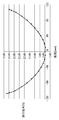
[光量プロファイル]
本実施形態に係る光走査装置400の被走査面407上におけるレーザスポット径は、軸上像高において60μm、最軸外像高において80μmである。上述したように、偏向器405と感光体4の被走査面407との距離は、偏向器405の主走査方向において端部側(最軸外像高)の方が遠いため、端部側になるに従ってスポット径が大きくなる。図8は、静止スポット光量プロファイルの例を示しており、縦軸が光量[arb]を示し、横軸が主走査方向位置[μm]を示す。また、図8中の実線は軸上像高における静止スポット光量プロファイルを示し、点線は最軸外像高における静止スポット光量プロファイルを示す。
[Light intensity profile]
The laser spot diameter on the surface to be scanned 407 of the
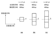
次に図13(a)に示す1×1ドット画像の軸上aに対応する主走査方向の積算光量プロファイルについて説明する。図13においては、軸が主走査方向に対応し、これに直交する方向を副走査方向として説明する。1×1ドットの主走査方向の積算プロファイルは図8に示す静止スポット光量プロファイルを主走査方向に1ドット(1画素分の幅:42.3μm)分足し合わせることで算出される。つまり、1×1ドットにおいては、他の隣接するドットが無いため、他のドットの積算光量プロファイルの影響は受けていない。 Next, the integrated light amount profile in the main scanning direction corresponding to the on axis a of the 1 × 1 dot image shown in FIG. 13A will be described. In FIG. 13, the axis corresponds to the main scanning direction, and the direction orthogonal to this is described as the sub-scanning direction. The integration profile of the 1 × 1 dot in the main scanning direction is calculated by adding the stationary spot light quantity profile shown in FIG. 8 by 1 dot (width of one pixel: 42.3 μm) in the main scanning direction. That is, since there is no other adjacent dot in 1 × 1 dot, it is not influenced by the integrated light amount profile of the other dots.
図13(b)は、主走査方向および副走査方向の解像度がそれぞれ600dpiである1×3ドットの縦線画像を示している。図13(c)は、主走査方向の解像度が600dpiであり、副走査方向の画像解像度が400dpiである1×3ドットの縦線画像を示している。 FIG. 13B shows a 1 × 3 dot vertical line image in which the resolutions in the main scanning direction and the sub scanning direction are each 600 dpi. FIG. 13C shows a 1 × 3 dot vertical line image in which the resolution in the main scanning direction is 600 dpi and the image resolution in the sub scanning direction is 400 dpi.
1×3ドットの縦線の積算光量プロファイルは、1×1ドット画像の積算光量プロファイルを副走査方向に3つ足し合わせることで算出される。また、軸上bにおける積算光量プロファイルは中央のドット以外のドット、すなわち上下に位置するドットの積算光量プロファイルの影響を受ける。ここで、副走査方向の解像度が400dpiの場合には、600dpiの場合に比べ、お互いの1×1ドットの積算光量プロファイルの重なり量が小さくなる。そのため、副走査方向の解像度が400dpiの場合の軸上bにおける主走査方向の積算光量プロファイルは、副走査方向の解像度が600dpiの場合の軸上bにおける主走査方向の積算光量プロファイルに比べピーク値は低くなり、また、裾野は狭くなる。 The integrated light amount profile of the 1 × 3 dot vertical line is calculated by adding three integrated light amount profiles of the 1 × 1 dot image in the sub-scanning direction. Further, the integrated light amount profile on the axis b is influenced by integrated light amount profiles of dots other than the central dot, that is, dots located at upper and lower positions. Here, when the resolution in the sub-scanning direction is 400 dpi, the overlapping amount of integrated light amount profiles of 1 × 1 dots of each other becomes smaller than in the case of 600 dpi. Therefore, the integrated light amount profile in the main scanning direction on the axis b when the resolution in the sub scanning direction is 400 dpi has a peak value compared to the integrated light amount profile in the main scanning direction on the axis b when the resolution in the sub scanning direction is 600 dpi. Will be lower and the skirt will be narrower.
図9に副走査方向の解像度が600dpiと400dpiの場合の積算光量プロファイルを示す。図9に示す各積算光量プロファイルにおいて、縦軸が積算光量[arb]を示し、横軸が主走査方向位置[μm]を示す。図9(a)、(b)、(c)は、副走査方向の解像度が600dpiの場合の1×3ドット画像の積算光量プロファイルを示す。一方、図9(d)、(e)、(f)は、副走査方向の解像度が400dpiの場合の積算光量プロファイルを示す。また、図9(a)、(d)は輝度がPの場合、図9(b)、(e)は輝度がP×1.5の場合、図9(c)、(f)は輝度がP×2.0の場合の軸上bにおける主走査方向の積算光量プロファイルをそれぞれ示している。 FIG. 9 shows integrated light quantity profiles when the resolution in the sub scanning direction is 600 dpi and 400 dpi. In each integrated light amount profile shown in FIG. 9, the vertical axis indicates the integrated light amount [arb], and the horizontal axis indicates the position in the main scanning direction [μm]. FIGS. 9A, 9B, and 9C show integrated light amount profiles of 1 × 3 dot images when the resolution in the sub scanning direction is 600 dpi. 9D, 9E, and 9F show integrated light amount profiles when the resolution in the sub scanning direction is 400 dpi. 9 (a) and 9 (d) show the case where the luminance is P, FIGS. 9 (b) and 9 (e) show the case where the luminance is P × 1.5, and FIGS. 9 (c) and 9 (f) show the luminance. The integrated light quantity profile in the main scanning direction on the axis b in the case of P × 2.0 is shown.
図9中の実線は軸上像高における積算光量プロファイルを、点線は最軸外像高における積算光量プロファイルを示す。図9に示すように、輝度によらず、最軸外像高の積算光量プロファイルの方が軸上像高の積算光量プロファイルに比べ、積算光量のピークが低く、プロファイルの裾野部分が広くなる。このように軸上像高と最軸外像高とで積算光量プロファイルが異なるのは、静止スポットの光量プロファイルが図8に示したように、軸上像高に比べ最軸外像高において、静止スポットの光量プロファイルのピーク値が低く、裾野が広いためである。また、同じ輝度おいて、副走査方向の解像度が異なる場合を比較すると、副走査方向の解像度が低い方が、ピーク値は低くなり、また、裾野は狭くなる。 The solid line in FIG. 9 indicates the integrated light amount profile at the axial image height, and the dotted line indicates the integrated light amount profile at the outermost off-axis image height. As shown in FIG. 9, regardless of the luminance, the peak of the integrated light amount is lower in the integrated light amount profile of the outermost off-axis image height compared to the integrated light amount profile of the on-axis image height, and the base portion of the profile is wider. The reason why the integrated light amount profile differs between the on-axis image height and the off-axis image height in this way is that the light amount profile of the stationary spot is different at the off-axis image height compared to the on-axis image height as shown in FIG. This is because the peak value of the light intensity profile of the stationary spot is low and the foot is wide. Further, comparing the case where the resolution in the sub scanning direction is different at the same luminance, the lower the resolution in the sub scanning direction, the lower the peak value and the narrower the base.
[E−V曲線]
図10は、本実施形態に係る感光体4(感光ドラム)の単位面積当たりのドラム面露光量とドラム電位の関係(E−V曲線)を示す。図10では、縦軸はドラム電位[−V]を示し、横軸はドラム面光量[μJ/cm2]を示す。図10に示すように、露光量が0、すなわち光源401が発光していない時の感光体4の表面電位は約−540Vであり、露光量を上げるほど、感光体4の電位は低く(絶対値は小さく)なる傾向がある。
[E-V curve]
FIG. 10 shows the relationship (EV curve) between the drum surface exposure amount per unit area of the photosensitive member 4 (photosensitive drum) according to this embodiment and the drum potential. In FIG. 10, the vertical axis indicates the drum potential [-V], and the horizontal axis indicates the drum surface light quantity [μJ / cm 2]. As shown in FIG. 10, the surface potential of the
[電位プロファイル]
図9に示す積算光量プロファイルと図10に示すE−V曲線を元に算出した電位プロファイルを図11に示す。図11に示す各電位プロファイルにおいて、縦軸がドラム電位[−V]を示し、横軸が主走査方向位置[μm]を示す。図11(a)、(b)、(c)は、副走査方向の解像度が600dpiの場合の1×3ドット画像の軸上bの感光体4の表面電位のプロファイルを示す。一方、図11(d)、(e)、(f)は、副走査方向の解像度が400dpiの場合の電位プロファイルを示す。また、図11(a)、(d)は輝度がPの場合、図11(b)、(e)は輝度がP×1.5の場合、図11(c)、(f)は輝度がP×2.0の場合の各軸上における主走査方向の電位プロファイルをそれぞれ示している。
[Potential profile]
The potential profile calculated based on the integrated light quantity profile shown in FIG. 9 and the EV curve shown in FIG. 10 is shown in FIG. In each potential profile shown in FIG. 11, the vertical axis indicates the drum potential [-V], and the horizontal axis indicates the position in the main scanning direction [μm]. 11A, 11 B, and 11 C show profiles of the surface potential of the
図11中の実線は軸上像高における電位プロファイルを、点線は最軸外像高における電位プロファイルを示す。図11に示すように、輝度によらず、最軸外像高の電位プロファイルの方が軸上像高の電位プロファイルに比べ、電位プロファイルのピーク値が低く、プロファイルの裾野部分が広くなる。このように軸上像高と最軸外像高とで電位プロファイルが異なるのは、図9に示したように、積算光量プロファイルが、軸上像高に比べ最軸外像高において、積算光量プロファイルのピーク値が低く、裾野が広いためである。 The solid line in FIG. 11 indicates the potential profile at the on-axis image height, and the dotted line indicates the potential profile at the outermost off-axis image height. As shown in FIG. 11, the peak value of the potential profile is lower in the potential profile of the outermost off-axis image height than the potential profile of the on-axis image height regardless of luminance, and the base portion of the profile is wider. The reason why the potential profile differs between the on-axis image height and the most off-axis image height in this way is that, as shown in FIG. 9, the integrated light quantity profile has an integrated light quantity at the most off-axis image height compared to the on-axis image height. This is because the peak value of the profile is low and the tail is wide.
図11における破線Vdcは本実施形態に係る現像電位(ここでは、−470V)を示し、図11の矢印の幅はドラム電位が現像電位以下となる部分の幅(以降、「現像幅」と呼ぶ)を示す。この現像幅は、後述するライン幅と相関があることが実験により証明されている。 The broken line Vdc in FIG. 11 indicates the developing potential (here, -470 V) according to this embodiment, and the width of the arrow in FIG. 11 is the width of a portion where the drum potential is equal to or less than the developing potential (hereinafter referred to as "developing width" ). It has been proved by experiment that this development width is correlated with the line width described later.
図11(a)、(d)に示すように、輝度がPの場合には最軸外像高の電位プロファイルは、軸上像高の電位プロファイルと比較して浅くなり、前述した現像幅は小さくなる。一方、図11(b)、(e)に示すように輝度がP×1.5の場合には、電位プロファイルが深くなることで、現像幅は大きくなる。特に、最軸外像高の方がより顕著に現像幅が大きくなる。理由は、最軸外像高の方が、電位プロファイルの裾野が広いため、輝度を上げた場合の現像幅への影響が大きくなるためである。更に輝度を上げ、図11(c)、(f)に示すように輝度をP×2.0とした場合には、輝度Pとした場合と大小関係が逆転し、軸上像高に対して最軸外像高の方が、現像幅が大きくなる。 As shown in FIGS. 11 (a) and 11 (d), when the luminance is P, the potential profile of the outermost off-axis image height is shallow compared to the potential profile of the on-axis image height, and the development width described above is It becomes smaller. On the other hand, as shown in FIGS. 11B and 11E, when the luminance is P × 1.5, the development width becomes large because the potential profile becomes deep. In particular, the development width increases more remarkably at the outermost off-axis image height. The reason is that since the base of the potential profile is wider at the outermost off-axis image height, the influence on the development width at the time of increasing the luminance is increased. When the luminance is further increased to P × 2.0 as shown in FIGS. 11 (c) and 11 (f), the magnitude relationship is reversed as compared with the luminance P, and the on-axis image height The development width is larger at the outermost off-axis image height.
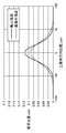
[ライン幅測定結果]
図12は、1×200ドットの縦線ライン画像を各主走査方向位置で印刷した際のライン幅の測定結果を示す。ここでのライン幅とは、主走査方向の1ドット(1画素)の長さに相当する。図12において、縦軸はライン幅測定結果[μm]を示し、横軸は主走査方向位置[mm]を示す。測定器としてはScanMateF10を使用した。本実施形態に係る結果1とともに、比較例として、比較例1、比較例2のライン幅測定結果も同様に示す。図12において(a)は、本実施形態の結果1としてのライン幅測定結果を示している。図12において(b)は比較例1としてのライン幅測定結果を示している。図12において(c)は比較例2としてのライン幅測定結果を示している。
[Line width measurement result]
FIG. 12 shows the measurement results of the line width when a 1 × 200 dot vertical line image is printed at each position in the main scanning direction. The line width here corresponds to the length of one dot (one pixel) in the main scanning direction. In FIG. 12, the vertical axis represents the line width measurement result [μm], and the horizontal axis represents the position in the main scanning direction [mm]. As a measuring instrument, ScanMateF10 was used. The line width measurement results of Comparative Example 1 and Comparative Example 2 are similarly shown as Comparative Example together with
各構成と各構成におけるライン幅評価結果を以下の表1に示す。各構成は単位面積当たりのドラム面光量と輝度、および、副走査方向の解像度の組み合わせが異なる。本実施形態に係る結果1と比較例1の単位面積当たりのドラム面光量は0.3μJ/cm2である。一方、比較例2においては、単位面積当たりのドラム面光量は、0.45μJ/cm2である。
Table 1 below shows the line width evaluation results for each configuration and each configuration. Each configuration differs in the combination of the drum surface light amount per unit area and the luminance, and the resolution in the sub scanning direction. The drum surface light quantity per unit area of the
また、比較例1の輝度をPとした場合、本実施形態に係る結果1と比較例2の輝度は1.5倍のP×1.5である。また、比較例1と比較例2は、副走査方向の解像度は600dpiに対して、本実施形態に係る結果1における副走査方向の解像度は400dpiである。なお、以下の説明において、解像度を600dpiと400dpiを例に挙げて説明するが、これに限定するものでは無い。
Moreover, when the brightness | luminance of the comparative example 1 is set to P, the brightness | luminance of the
ここで、副走査方向の解像度が600dpiの場合と400dpiの場合で偏向器405の回転数は同一である。一方、プロセススピード、すなわち、感光体4の回転速度は副走査方向の解像度が600dpiの場合に対し、400dpiの場合において1.5倍としている。そのため、単位面積当たりのドラム面光量は、本実施形態に係る結果1と比較例1とは等しくなる。

図12の(b)に示すように比較例1の構成においては最軸外像高におけるライン幅は、軸上像高のライン幅と比較して、細くなっている。これは、図11(a)の1×3ドット画像の電位プロファイルが示すように、軸上像高における現像幅と比較して、最軸外像高における現像幅が狭くなるためである。 As shown in (b) of FIG. 12, in the configuration of Comparative Example 1, the line width at the outermost off-axis image height is narrower than the line width at the on-axis image height. This is because, as shown in the potential profile of the 1 × 3 dot image in FIG. 11A, the development width at the outermost off-axis image height is narrower than the development width at the on-axis image height.
一方、図12の(c)に示すように、比較例2においてライン幅は各像高でほぼ均一になる。これは、図11(b)の1×3ドット画像の電位プロファイルが示すように、現像幅が軸上像高と最軸外像高でほぼ同一となるためである。しかしながら、比較例2の場合においてはライン幅が像高によらず均一となるものの、ライン幅自体が適正値よりも太くなるため、ライン画像として適さない。このような構成では、例えば、1ドットの白抜き文字を印刷した場合に白抜き部分が不明瞭になってしまうという問題が生じる。 On the other hand, as shown in (c) of FIG. 12, in Comparative Example 2, the line width is substantially uniform at each image height. This is because, as shown by the potential profile of the 1 × 3 dot image in FIG. 11B, the development width is substantially the same between the on-axis image height and the most off-axis image height. However, in the case of Comparative Example 2, although the line width is uniform regardless of the image height, the line width itself becomes thicker than the appropriate value, and therefore, it is not suitable as a line image. In such a configuration, for example, there is a problem that the white portion becomes unclear when one-dot white character is printed.
一方、本実施形態に係る構成とすることで、図12の(a)に示すようにライン均一性を保ちつつ、ライン幅を適正値とすることができる。これは、輝度をP×1.5とし、副走査方向の解像度を400dpiとすることで、ライン幅を像高によらず均一とするとともに、ライン幅自体が適正値よりも太くなることを抑制しているためである。 On the other hand, with the configuration according to the present embodiment, the line width can be set to an appropriate value while maintaining the line uniformity as shown in FIG. By setting the luminance to P × 1.5 and the resolution in the sub scanning direction to 400 dpi, the line width is made uniform regardless of the image height, and the line width itself is prevented from becoming thicker than the appropriate value. It is because
以上述べたように、各像高に応じてスポット径が異なる光走査装置を用いた場合であっても、本実施形態では、ライン幅が中央と端部で略等しくなるように、輝度を調節した上で、副走査方向の解像度を主走査方向に対して低くしている。これにより、主走査方向位置に応じて、ライン幅が変わってしまうことを抑制するとともに、適正なライン幅とすることができる。 As described above, even in the case where light scanning devices having different spot diameters according to each image height are used, in the present embodiment, the brightness is adjusted so that the line width becomes substantially equal at the center and at the end. In addition, the resolution in the sub-scanning direction is lowered relative to the main scanning direction. Thus, the line width can be prevented from changing according to the position in the main scanning direction, and the line width can be made appropriate.
<第2実施形態>
第1実施形態においては入力画像データに応じて、PWM値を図7に示すように制御していた。これに対し、第2実施形態では、例えば、第1実施形態にて用いたPWM値をPWMとした場合、PWM値をPWM×400dpi/600dpi=PWM×2/3に制御する。例えば、第1実施形態のパルス信号のテーブルにおける最高画像階調(すなわち、レベル31)におけるPWM値は“255”であるのに対し、本実施形態のレベル31におけるPWM値は“170”である点が異なる。
Second Embodiment
In the first embodiment, the PWM value is controlled as shown in FIG. 7 according to the input image data. On the other hand, in the second embodiment, when the PWM value used in the first embodiment is PWM, for example, the PWM value is controlled to PWM × 400 dpi / 600 dpi = PWM × 2/3. For example, while the PWM value at the highest image gradation (ie, level 31) in the table of pulse signals of the first embodiment is "255", the PWM value at
本実施形態においては、1画素ごとに発光と非発光が一定の比率で繰り返される。具体的には、上記の制御内容に基づくと、
発光時間:非発光時間=170:(255−170)=2:1
の比率で発光と非発光を1画素毎に繰り返す。これにより、例えば、最高画像階調における1画素に対する光量が“170”に相当する値となる。なお、1画素において、非発光動作と発光動作のいずれを先に行ってもよい。
In the present embodiment, light emission and non-light emission are repeated at a constant ratio for each pixel. Specifically, based on the above control contents,
Light emission time: Non-light emission time = 170: (255-170) = 2: 1
Light emission and non-light emission are repeated for each pixel at a ratio of Thereby, for example, the light quantity for one pixel in the highest image gradation becomes a value corresponding to "170". Note that in one pixel, either the non-light emitting operation or the light emitting operation may be performed first.
また、第1実施形態における副走査方向の画像解像度は400dpiであるのに対し、本実施形態における副走査方向の画像解像度は600dpiである点が異なる。また、本実施形態においても、主走査方向の画像解像度は600dpiである。レーザ輝度は、本実施形態においても、第1実施形態と同様にP×1.5である。その他の構成に関しては第1実施形態と同様であるため、詳細な説明は省略する。 Further, while the image resolution in the sub-scanning direction in the first embodiment is 400 dpi, the image resolution in the sub-scanning direction in the present embodiment is 600 dpi. Also in the present embodiment, the image resolution in the main scanning direction is 600 dpi. The laser brightness in this embodiment is P × 1.5 as in the first embodiment. The other configuration is the same as that of the first embodiment, and thus the detailed description will be omitted.
本実施形態の構成により、副走査方向の画像解像度が主走査方向の画像解像度と同じである場合に、第1実施形態と同様に主走査方向位置に応じて、ライン幅が変わってしまうことを抑制するとともに、適正なライン幅とすることができる。具体的には、本実施形態の構成により、第1実施形態の図12で説明した比較例2で問題となったライン自体が適正値よりも太くなってしまうことを抑制することができる。 According to the configuration of this embodiment, when the image resolution in the sub scanning direction is the same as the image resolution in the main scanning direction, the line width may be changed according to the position in the main scanning direction as in the first embodiment. While suppressing, it can be set as an appropriate line width. Specifically, with the configuration of the present embodiment, it is possible to suppress that the line itself, which becomes a problem in the comparative example 2 described in FIG. 12 of the first embodiment, becomes thicker than the appropriate value.
以下、上記の理由を説明する。図13(b)に示す1×3ドット画像の軸上bにおける、本実施形態に係る積算光量プロファイルを図14に示す。図14において、縦軸は積算光量[arb]を示し、横軸は主走査方向位置[μm]を示す。一方、図9(b)に示す積算光量プロファイルは比較例2の積算光量プロファイルである。本実施形態に係る図14の積算光量プロファイルと、図9(b)に示す比較例2の積算光量プロファイルはいずれも、副走査解像度が600dpiであり、輝度がP×1.5の場合である。図14の積算光量プロファイルは図9(b)の積算光量プロファイルと比較して、ピーク値が低く、裾野も狭くなる。図9(b)はPWM値が“255”であり、主走査方向に約42.3μm分(1画素分)の静止スポット光量プロファイルが積算される。これに対し、本実施形態の場合にはPWM値が“170”であり、主走査方向に約28.2μm分のみ、静止スポット光量プロファイルが積算される。そのため、図14のような構成となる。 Hereinafter, the above reasons will be described. FIG. 14 shows an integrated light quantity profile according to the present embodiment on the axis b of the 1 × 3 dot image shown in FIG. In FIG. 14, the vertical axis represents the integrated light quantity [arb], and the horizontal axis represents the position in the main scanning direction [μm]. On the other hand, the integrated light amount profile shown in FIG. 9B is the integrated light amount profile of Comparative Example 2. Both the integrated light amount profile of FIG. 14 according to the present embodiment and the integrated light amount profile of Comparative Example 2 shown in FIG. 9 (b) have a sub-scanning resolution of 600 dpi and a luminance of P × 1.5. . Compared with the integrated light amount profile of FIG. 9B, the integrated light amount profile of FIG. 14 has a lower peak value and a narrower base. In FIG. 9B, the PWM value is “255”, and the static spot light intensity profile of about 42.3 μm (one pixel) in the main scanning direction is integrated. On the other hand, in the case of the present embodiment, the PWM value is "170", and the stationary spot light quantity profile is integrated only for about 28.2 μm in the main scanning direction. Therefore, the configuration is as shown in FIG.
図15は、図13(b)に示す1×3ドット画像の軸上bにおける、本実施形態に係る電位プロファイルを示す。図15において、縦軸はドラム電位[−V]を示し、横軸は主走査方向位置[μm]を示す。一方、図11(b)に示す電位プロファイルは比較例2の電位プロファイルである。本実施形態に係る図15の電位プロファイルと、図11(b)に示す比較例2の電位プロファイルはいずれも、副走査解像度が600dpiであり、輝度がP×1.5の場合である。図15の電位プロファイルは図11(b)の電位プロファイルと比較して、ピーク値が低く、裾野も狭くなる。 FIG. 15 shows a potential profile according to the present embodiment on the axis b of the 1 × 3 dot image shown in FIG. 13 (b). In FIG. 15, the vertical axis indicates the drum potential [-V], and the horizontal axis indicates the position in the main scanning direction [μm]. On the other hand, the potential profile shown in FIG. 11B is the potential profile of Comparative Example 2. Both the potential profile of FIG. 15 and the potential profile of Comparative Example 2 shown in FIG. 11B according to this embodiment have a sub-scanning resolution of 600 dpi and a luminance of P × 1.5. Compared with the potential profile of FIG. 11B, the potential profile of FIG. 15 has a lower peak value and a narrower skirt.
図16は、本実施形態に係るライン幅測定結果を示す。図16において(a)は、本実施形態の結果2としてのライン幅測定結果を示している。図16において(b)は、比較例2としてのライン測定結果を示している。上述したように、本実施形態の結果2も比較例2も主走査解像度、副走査解像度がともに600dpiであり、輝度がP×1.5の場合を示している。
FIG. 16 shows line width measurement results according to the present embodiment. In FIG. 16, (a) shows the line width measurement result as the
図16に示されているように、本実施形態の構成により、主走査方向位置に応じて、ライン幅が変わってしまうことを抑制するとともに、適正なライン幅とすることができる。これは、図15の電位プロファイルからも明らかである。 As shown in FIG. 16, according to the configuration of the present embodiment, it is possible to suppress the line width from being changed according to the position in the main scanning direction, and to make the line width appropriate. This is also apparent from the potential profile of FIG.
<第3実施形態>
第3実施形態として、副走査方向の画像解像度に応じて、PWM値を切り換える機能を有する実施形態について説明する。つまり、画像形成装置は、副走査方向の画像解像度を切り替えた複数のモードにて画像形成を行うことが可能であり、切り替えた際に、PWM値も切り替える構成とする。なお、第1、第2実施形態と同様の構成については、詳細な説明を省略する。
Third Embodiment
As a third embodiment, an embodiment having a function of switching the PWM value according to the image resolution in the sub-scanning direction will be described. That is, the image forming apparatus can perform image formation in a plurality of modes in which the image resolution in the sub-scanning direction is switched, and when switching is performed, the PWM value is also switched. In addition, detailed description is abbreviate | omitted about the structure similar to 1st, 2nd embodiment.
[処理フロー]
図17は、本実施形態に係るPWM値の切り替え処理を示すフローチャートである。本処理フローは、複数の処理部が連携して制御を行うため、ここでは、処理主体を画像形成装置9として説明する。
Processing flow
FIG. 17 is a flowchart showing PWM value switching processing according to the present embodiment. In the present processing flow, since a plurality of processing units perform control in cooperation, the processing subject is described as the
画像形成装置9は、ユーザからプリンタードライバー(不図示)を介して、副走査方向の画像解像度情報を取得すると、副走査方向の画像解像度情報に応じたプロセススピードを設定し、画像形成装置を動作させる。ここでは、400dpiもしくは600dpiのいずれかの値が副走査方向の画像解像度として指定されるものとして説明を行う。なお、以下に示すプロセススピードPS、偏向器405の回転数F、輝度Pは、予め規定され、その情報が画像形成装置9にて保持されているものとする。
When image resolution information in the sub scanning direction is acquired from the user via a printer driver (not shown) from the user, the
S1701にて、画像形成装置9は、指定された副走査方向の画像解像度が400dpiか否かを判定する。400dpiが指定された場合(S1701にてYES)S1702へ進み、600dpiが指定された場合(S1701にてNO)S1706へ進む。
In S1701, the
S1702にて、画像形成装置9は、プロセススピードをPSに設定する。具体的には、感光体4の回転速度を120mm/sに設定する。
In S1702, the
S1703にて、画像形成装置9は、偏向器405の回転速度が副走査方向の画像解像度情報によらず、一定の回転数Fに収束させるように駆動部(不図示)を制御する。
In S1703, the
S1704にて、画像形成装置9は、光源401の発光輝度が副走査方向の画像解像度情報によらず、輝度P×1.5(=600/400)となるように制御する。
In S1704, the
S1705にて、画像形成装置9は、最高画像階調のPWM値を255に設定する。これに合せて、画像の各階調のPWM値を設定する。つまり、第1実施形態にて図7を用いた構成となるように設定する。そして、本処理フローを終了する。
At S1705, the
S1706にて、画像形成装置9は、プロセススピードを(PS×400/600)に設定する。具体的には、感光体4の回転速度を80mm/sに設定する。
At S1706, the
S1707にて、画像形成装置9は、偏向器405の回転速度が副走査方向の画像解像度情報によらず、一定の回転数Fに収束させるように駆動部(不図示)を制御する。
In S1707, the
S1708にて、画像形成装置9は、光源401の発光輝度が副走査方向の画像解像度情報によらず、輝度P×1.5(=600/400)となるように制御する。
In S1708, the
S1709にて、画像形成装置9は、最高画像階調のPWM値が170(=255×400/600)となるように制御する。これに合せて、画像の各階調のPWM値に2/3の重み付けした値となるように制御する。つまり、第2実施形態にて説明した構成となるように設定する。そして、本処理フローを終了する。
At S1709, the
以上、本実施形態の構成により、副走査方向の画像解像度に係らず、主走査方向位置に応じて、ライン幅が変わってしまうことを抑制するとともに、適正なライン幅とすることができる。 As described above, with the configuration of the present embodiment, regardless of the image resolution in the sub scanning direction, the line width can be suppressed from changing according to the position in the main scanning direction, and the line width can be made appropriate.
なお、上記の構成では、主走査方向と副走査方向の解像度において、600dpiと400dpiを例に挙げて説明したが、この組み合わせに限定するものでははく、他の構成であってもよい。また、図3に示した像高と部分倍率の関係は一例であり、この関係性の変動に応じて各種制御に用いる情報は定義されてよい。例えば、副走査方向の解像度がAdpiの場合とB(>A)dpiの場合を考える。このとき、Aの場合のPWM値を“255”とした場合、Bの場合のPWM値は“255×(A/B)”として制御される。このときのある走査位置におけるレーザ光の発光と非発光の比は、255×(A/B):{255−(255×(A/B))}=(A/B):{1−(A/B)}となる。また、レーザ光の輝度Pは(B/A)となるように制御される。 In the above-described configuration, 600 dpi and 400 dpi have been described by way of example in the resolutions in the main scanning direction and the sub scanning direction, but the present invention is not limited to this combination, and other configurations may be used. Further, the relationship between the image height and the partial magnification shown in FIG. 3 is an example, and information used for various controls may be defined according to the fluctuation of the relationship. For example, consider the case where the resolution in the sub-scanning direction is Adpi and the case where B (> A) dpi. At this time, assuming that the PWM value in the case of A is “255”, the PWM value in the case of B is controlled as “255 × (A / B)”. The ratio of light emission to non-light emission of laser light at a certain scanning position at this time is 255 × (A / B): {255− (255 × (A / B))} = (A / B): {1− A / B)}. Further, the luminance P of the laser light is controlled to be (B / A).
<その他の実施形態>
本発明は上述の実施形態の1以上の機能を実現するプログラムをネットワーク又は記憶媒体を介してシステム又は装置に供給し、そのシステム又は装置のコンピュータにおける1つ以上のプロセッサがプログラムを読出し実行する処理でも実現可能である。また、1以上の機能を実現する回路(例えば、ASIC)によっても実現可能である。
<Other Embodiments>
The present invention supplies a program that implements one or more functions of the above-described embodiments to a system or apparatus via a network or storage medium, and one or more processors in a computer of the system or apparatus read and execute the program. But it is possible. It can also be implemented by a circuit (eg, an ASIC) that implements one or more functions.
4…感光体、9…画像形成装置、100…画像信号生成部、101…画像処理部、101a…中間調処理部(ハーフトーン処理手段)、101z…濃度補正処理部、208…レーザ光(光)、400…光走査装置(走査手段)
Claims (15)
前記感光体を帯電させる帯電手段と、
前記感光体の主走査方向の走査位置に応じてスポット径が異なるレーザ光により前記感光体を走査して潜像を形成する露光手段と、
前記潜像が形成された前記感光体にトナーを付着させて現像を行う現像手段と、
を有する画像形成装置であって、
前記感光体の主走査方向の走査位置に応じて、前記レーザ光の輝度と、前記感光体の副走査方向の解像度を制御する制御手段を備えることを特徴とする画像形成装置。 A photoconductor,
Charging means for charging the photosensitive member;
An exposure unit configured to scan the photosensitive member with laser light having a different spot diameter depending on a scanning position in the main scanning direction of the photosensitive member to form a latent image;
Developing means for causing toner to adhere to the photosensitive member on which the latent image is formed, and performing development;
An image forming apparatus having
An image forming apparatus comprising: control means for controlling the brightness of the laser beam and the resolution in the sub scanning direction of the photosensitive member according to the scanning position in the main scanning direction of the photosensitive member.
前記感光体を帯電させる帯電手段と、
前記感光体の主走査方向の走査位置に応じてスポット径が異なるレーザ光により前記感光体を走査して潜像を形成する露光手段と、
前記潜像が形成された前記感光体にトナーを付着させて現像を行う現像手段と、
を有する画像形成装置であって、
前記感光体の主走査方向における画素の位置ごとに、前記レーザ光の輝度と、前記レーザ光の発光時間とを制御する制御手段を備えることを特徴とする画像形成装置。 A photoconductor,
Charging means for charging the photosensitive member;
An exposure unit configured to scan the photosensitive member with laser light having a different spot diameter depending on a scanning position in the main scanning direction of the photosensitive member to form a latent image;
Developing means for causing toner to adhere to the photosensitive member on which the latent image is formed, and performing development;
An image forming apparatus having
An image forming apparatus comprising: control means for controlling the brightness of the laser light and the light emission time of the laser light for each position of a pixel in the main scanning direction of the photosensitive member.
第1のモードの副走査方向の解像度がAであり、第2のモードの副走査方向の解像度がB(>A)であり、前記第1のモードのプロセススピードをPSとした場合、
前記第2のモードのプロセススピードをPS×A/Bとし、
前記第2のモードでは、前記感光体の主走査方向の走査位置それぞれにおいて、対応する画像データの値に(A/B)の重み付けをした値に対応する光量となるように、前記レーザ光の露光を制御することを特徴とする請求項1乃至7のいずれか一項に記載の画像形成装置。 The image forming apparatus can perform image formation in a plurality of modes in which the resolution in the sub scanning direction of the photosensitive member is switched.
Assuming that the resolution in the sub-scanning direction of the first mode is A, the resolution in the sub-scanning direction of the second mode is B (> A), and the process speed of the first mode is PS
The process speed of the second mode is PS × A / B,
In the second mode, at each scanning position in the main scanning direction of the photosensitive member, the amount of the laser light corresponds to a value obtained by weighting the value of the corresponding image data with (A / B). The image forming apparatus according to any one of claims 1 to 7, which controls exposure.
前記感光体を帯電させる帯電手段と、
前記感光体の主走査方向の走査位置に応じてスポット径が異なるレーザ光により前記感光体を走査して潜像を形成する露光手段と、
前記潜像が形成された前記感光体にトナーを付着させて現像を行う現像手段と、
を有する画像形成装置の制御方法であって、
前記感光体の主走査方向の走査位置に応じて、前記レーザ光の輝度と、前記感光体の副走査方向の解像度を制御することを特徴とする画像形成装置の制御方法。 A photoconductor,
Charging means for charging the photosensitive member;
An exposure unit configured to scan the photosensitive member with laser light having a different spot diameter depending on a scanning position in the main scanning direction of the photosensitive member to form a latent image;
Developing means for causing toner to adhere to the photosensitive member on which the latent image is formed, and performing development;
A control method of an image forming apparatus having
A control method of an image forming apparatus, comprising: controlling the brightness of the laser beam and the resolution in the sub scanning direction of the photosensitive member according to a scanning position in the main scanning direction of the photosensitive member.
前記感光体を帯電させる帯電手段と、
前記感光体の主走査方向の走査位置に応じてスポット径が異なるレーザ光により前記感光体を走査して潜像を形成する露光手段と、
前記潜像が形成された前記感光体にトナーを付着させて現像を行う現像手段と、
を有する画像形成装置の制御方法であって、
前記感光体の主走査方向における画素の位置ごとに、前記レーザ光の輝度と、前記レーザ光の発光時間とを制御することを特徴とする画像形成装置の制御方法。 A photoconductor,
Charging means for charging the photosensitive member;
An exposure unit configured to scan the photosensitive member with laser light having a different spot diameter depending on a scanning position in the main scanning direction of the photosensitive member to form a latent image;
Developing means for causing toner to adhere to the photosensitive member on which the latent image is formed, and performing development;
A control method of an image forming apparatus having
A control method of an image forming apparatus, comprising: controlling the brightness of the laser beam and the light emission time of the laser beam for each position of a pixel in the main scanning direction of the photosensitive member.
Priority Applications (3)
| Application Number | Priority Date | Filing Date | Title |
|---|---|---|---|
| JP2018006691A JP2019124873A (en) | 2018-01-18 | 2018-01-18 | Image forming apparatus and method for controlling the same |
| US16/247,395 US10520849B2 (en) | 2018-01-18 | 2019-01-14 | Image forming apparatus and control method thereof |
| JP2022200503A JP2023051967A (en) | 2018-01-18 | 2022-12-15 | Image forming apparatus and method for controlling the same |
Applications Claiming Priority (1)
| Application Number | Priority Date | Filing Date | Title |
|---|---|---|---|
| JP2018006691A JP2019124873A (en) | 2018-01-18 | 2018-01-18 | Image forming apparatus and method for controlling the same |
Related Child Applications (1)
| Application Number | Title | Priority Date | Filing Date |
|---|---|---|---|
| JP2022200503A Division JP2023051967A (en) | 2018-01-18 | 2022-12-15 | Image forming apparatus and method for controlling the same |
Publications (2)
| Publication Number | Publication Date |
|---|---|
| JP2019124873A true JP2019124873A (en) | 2019-07-25 |
| JP2019124873A5 JP2019124873A5 (en) | 2021-04-01 |
Family
ID=67213854
Family Applications (2)
| Application Number | Title | Priority Date | Filing Date |
|---|---|---|---|
| JP2018006691A Pending JP2019124873A (en) | 2018-01-18 | 2018-01-18 | Image forming apparatus and method for controlling the same |
| JP2022200503A Pending JP2023051967A (en) | 2018-01-18 | 2022-12-15 | Image forming apparatus and method for controlling the same |
Family Applications After (1)
| Application Number | Title | Priority Date | Filing Date |
|---|---|---|---|
| JP2022200503A Pending JP2023051967A (en) | 2018-01-18 | 2022-12-15 | Image forming apparatus and method for controlling the same |
Country Status (2)
| Country | Link |
|---|---|
| US (1) | US10520849B2 (en) |
| JP (2) | JP2019124873A (en) |
Families Citing this family (1)
| Publication number | Priority date | Publication date | Assignee | Title |
|---|---|---|---|---|
| CN113284395B (en) * | 2021-05-19 | 2022-12-02 | 山东电子职业技术学院 | Laser pen for multimedia teaching |
Citations (3)
| Publication number | Priority date | Publication date | Assignee | Title |
|---|---|---|---|---|
| JPH09323443A (en) * | 1996-06-07 | 1997-12-16 | Canon Inc | Led printer and density adjusting method for the same |
| JP2006154337A (en) * | 2004-11-30 | 2006-06-15 | Konica Minolta Business Technologies Inc | Laser scanning optical system |
| JP2016000511A (en) * | 2014-06-12 | 2016-01-07 | キヤノン株式会社 | Image forming device |
Family Cites Families (8)
| Publication number | Priority date | Publication date | Assignee | Title |
|---|---|---|---|---|
| JPS6125164A (en) | 1984-07-13 | 1986-02-04 | Fujitsu Ltd | Printing device |
| JP2000351234A (en) | 1999-06-11 | 2000-12-19 | Hitachi Koki Co Ltd | Apparatus for controlling laser of electrophotographic apparatus |
| US7675532B2 (en) | 2007-09-28 | 2010-03-09 | Canon Kabushiki Kaisha | Image-forming apparatus and control method thereof |
| EP3722880B1 (en) | 2014-06-12 | 2022-10-05 | Canon Kabushiki Kaisha | Image-forming apparatus |
| JP6489861B2 (en) * | 2015-02-19 | 2019-03-27 | キヤノン株式会社 | Image forming apparatus |
| JP6700744B2 (en) | 2015-11-26 | 2020-05-27 | キヤノン株式会社 | Image forming apparatus and control method thereof |
| JP6706144B2 (en) | 2016-05-27 | 2020-06-03 | キヤノン株式会社 | Image forming device |
| JP6836308B2 (en) * | 2017-05-15 | 2021-02-24 | キヤノン株式会社 | Image forming device |
-
2018
- 2018-01-18 JP JP2018006691A patent/JP2019124873A/en active Pending
-
2019
- 2019-01-14 US US16/247,395 patent/US10520849B2/en active Active
-
2022
- 2022-12-15 JP JP2022200503A patent/JP2023051967A/en active Pending
Patent Citations (3)
| Publication number | Priority date | Publication date | Assignee | Title |
|---|---|---|---|---|
| JPH09323443A (en) * | 1996-06-07 | 1997-12-16 | Canon Inc | Led printer and density adjusting method for the same |
| JP2006154337A (en) * | 2004-11-30 | 2006-06-15 | Konica Minolta Business Technologies Inc | Laser scanning optical system |
| JP2016000511A (en) * | 2014-06-12 | 2016-01-07 | キヤノン株式会社 | Image forming device |
Also Published As
| Publication number | Publication date |
|---|---|
| US20190219942A1 (en) | 2019-07-18 |
| JP2023051967A (en) | 2023-04-11 |
| US10520849B2 (en) | 2019-12-31 |
Similar Documents
| Publication | Publication Date | Title |
|---|---|---|
| JP6836308B2 (en) | Image forming device | |
| US9665031B2 (en) | Image forming apparatus that forms latent image by irradiating photosensitive member with light | |
| JP6261453B2 (en) | Image forming apparatus | |
| JP6706144B2 (en) | Image forming device | |
| US8605131B2 (en) | Image forming apparatus and image forming method | |
| US9091956B2 (en) | Image forming apparatus for performing exposure a plurality of times | |
| JP2023051967A (en) | Image forming apparatus and method for controlling the same | |
| JP2022159275A (en) | Image forming apparatus | |
| JP7030889B2 (en) | Image forming device | |
| JP6594142B2 (en) | Image forming apparatus, image forming method, and program | |
| JP2008012852A (en) | Image forming device | |
| JP6727913B2 (en) | Image forming device | |
| JP2018089866A (en) | Image formation apparatus and image formation method | |
| JP6812216B2 (en) | Image forming device | |
| JP2018069682A (en) | Image forming apparatus | |
| JP2018001588A (en) | Image formation apparatus | |
| JP2020204702A (en) | Image forming apparatus | |
| JP2017030309A (en) | Image forming apparatus, and method for controlling image forming apparatus | |
| JP6740796B2 (en) | Information processing device, pixel setting method, and program | |
| JP2021151714A (en) | Image forming device | |
| JP2017223733A (en) | Information processing apparatus, image forming apparatus, image processing method, and program | |
| JP2017223732A (en) | Image forming apparatus and image forming method | |
| JP2013141798A (en) | Image forming apparatus and control method for the image forming apparatus | |
| JP2017191208A (en) | Image forming apparatus, information processing method, and program | |
| JP2013011765A (en) | Image forming apparatus and image forming method |
Legal Events
| Date | Code | Title | Description |
|---|---|---|---|
| RD01 | Notification of change of attorney |
Free format text: JAPANESE INTERMEDIATE CODE: A7421 Effective date: 20210103 |
|
| A521 | Request for written amendment filed |
Free format text: JAPANESE INTERMEDIATE CODE: A523 Effective date: 20210113 |
|
| A521 | Request for written amendment filed |
Free format text: JAPANESE INTERMEDIATE CODE: A523 Effective date: 20210115 |
|
| A621 | Written request for application examination |
Free format text: JAPANESE INTERMEDIATE CODE: A621 Effective date: 20210115 |
|
| A977 | Report on retrieval |
Free format text: JAPANESE INTERMEDIATE CODE: A971007 Effective date: 20211026 |
|
| A131 | Notification of reasons for refusal |
Free format text: JAPANESE INTERMEDIATE CODE: A131 Effective date: 20211101 |
|
| A521 | Request for written amendment filed |
Free format text: JAPANESE INTERMEDIATE CODE: A523 Effective date: 20211221 |
|
| A131 | Notification of reasons for refusal |
Free format text: JAPANESE INTERMEDIATE CODE: A131 Effective date: 20220506 |
|
| A521 | Request for written amendment filed |
Free format text: JAPANESE INTERMEDIATE CODE: A523 Effective date: 20220704 |
|
| A02 | Decision of refusal |
Free format text: JAPANESE INTERMEDIATE CODE: A02 Effective date: 20220916 |