JP2019096902A - Method for manufacturing semiconductor component and semiconductor component - Google Patents
Method for manufacturing semiconductor component and semiconductor component Download PDFInfo
- Publication number
- JP2019096902A JP2019096902A JP2019024750A JP2019024750A JP2019096902A JP 2019096902 A JP2019096902 A JP 2019096902A JP 2019024750 A JP2019024750 A JP 2019024750A JP 2019024750 A JP2019024750 A JP 2019024750A JP 2019096902 A JP2019096902 A JP 2019096902A
- Authority
- JP
- Japan
- Prior art keywords
- semiconductor
- layer
- contact
- support
- contact area
- Prior art date
- Legal status (The legal status is an assumption and is not a legal conclusion. Google has not performed a legal analysis and makes no representation as to the accuracy of the status listed.)
- Granted
Links
- 239000004065 semiconductor Substances 0.000 title claims abstract description 346
- 238000000034 method Methods 0.000 title abstract description 63
- 238000004519 manufacturing process Methods 0.000 title abstract description 50
- 238000004873 anchoring Methods 0.000 claims description 39
- 239000000463 material Substances 0.000 claims description 33
- 230000005855 radiation Effects 0.000 claims description 18
- 239000002245 particle Substances 0.000 claims description 8
- 239000000853 adhesive Substances 0.000 claims description 7
- 230000001070 adhesive effect Effects 0.000 claims description 7
- 239000012212 insulator Substances 0.000 claims description 6
- OAICVXFJPJFONN-UHFFFAOYSA-N Phosphorus Chemical compound [P] OAICVXFJPJFONN-UHFFFAOYSA-N 0.000 claims description 5
- 238000007789 sealing Methods 0.000 claims description 5
- 229910052751 metal Inorganic materials 0.000 claims description 4
- 239000002184 metal Substances 0.000 claims description 4
- 239000011159 matrix material Substances 0.000 claims description 3
- 238000005304 joining Methods 0.000 claims description 2
- 229910000679 solder Inorganic materials 0.000 claims description 2
- 239000012780 transparent material Substances 0.000 claims description 2
- 239000000758 substrate Substances 0.000 abstract description 144
- 239000010410 layer Substances 0.000 description 215
- 229920002120 photoresistant polymer Polymers 0.000 description 14
- 238000005530 etching Methods 0.000 description 12
- 230000005670 electromagnetic radiation Effects 0.000 description 10
- 238000002161 passivation Methods 0.000 description 9
- 150000001875 compounds Chemical class 0.000 description 8
- 229910052581 Si3N4 Inorganic materials 0.000 description 5
- VYPSYNLAJGMNEJ-UHFFFAOYSA-N Silicium dioxide Chemical compound O=[Si]=O VYPSYNLAJGMNEJ-UHFFFAOYSA-N 0.000 description 5
- 239000012790 adhesive layer Substances 0.000 description 5
- 230000015572 biosynthetic process Effects 0.000 description 5
- HQVNEWCFYHHQES-UHFFFAOYSA-N silicon nitride Chemical compound N12[Si]34N5[Si]62N3[Si]51N64 HQVNEWCFYHHQES-UHFFFAOYSA-N 0.000 description 5
- 229910052814 silicon oxide Inorganic materials 0.000 description 5
- XUIMIQQOPSSXEZ-UHFFFAOYSA-N Silicon Chemical compound [Si] XUIMIQQOPSSXEZ-UHFFFAOYSA-N 0.000 description 4
- 238000001312 dry etching Methods 0.000 description 4
- 238000000206 photolithography Methods 0.000 description 4
- 239000011241 protective layer Substances 0.000 description 4
- 229910052710 silicon Inorganic materials 0.000 description 4
- 239000010703 silicon Substances 0.000 description 4
- 230000008878 coupling Effects 0.000 description 3
- 238000010168 coupling process Methods 0.000 description 3
- 238000005859 coupling reaction Methods 0.000 description 3
- 230000001419 dependent effect Effects 0.000 description 3
- 230000000694 effects Effects 0.000 description 3
- 238000000059 patterning Methods 0.000 description 3
- 229920000642 polymer Polymers 0.000 description 3
- 229910052594 sapphire Inorganic materials 0.000 description 3
- 239000010980 sapphire Substances 0.000 description 3
- KDLHZDBZIXYQEI-UHFFFAOYSA-N Palladium Chemical compound [Pd] KDLHZDBZIXYQEI-UHFFFAOYSA-N 0.000 description 2
- 229910052782 aluminium Inorganic materials 0.000 description 2
- 238000004140 cleaning Methods 0.000 description 2
- 238000000576 coating method Methods 0.000 description 2
- 238000010586 diagram Methods 0.000 description 2
- 239000003989 dielectric material Substances 0.000 description 2
- 238000000227 grinding Methods 0.000 description 2
- BASFCYQUMIYNBI-UHFFFAOYSA-N platinum Chemical compound [Pt] BASFCYQUMIYNBI-UHFFFAOYSA-N 0.000 description 2
- 238000000926 separation method Methods 0.000 description 2
- 239000002904 solvent Substances 0.000 description 2
- 238000004528 spin coating Methods 0.000 description 2
- 239000000126 substance Substances 0.000 description 2
- 229910002601 GaN Inorganic materials 0.000 description 1
- JMASRVWKEDWRBT-UHFFFAOYSA-N Gallium nitride Chemical compound [Ga]#N JMASRVWKEDWRBT-UHFFFAOYSA-N 0.000 description 1
- 229910004298 SiO 2 Inorganic materials 0.000 description 1
- BQCADISMDOOEFD-UHFFFAOYSA-N Silver Chemical compound [Ag] BQCADISMDOOEFD-UHFFFAOYSA-N 0.000 description 1
- 230000002411 adverse Effects 0.000 description 1
- 229910045601 alloy Inorganic materials 0.000 description 1
- 239000000956 alloy Substances 0.000 description 1
- XAGFODPZIPBFFR-UHFFFAOYSA-N aluminium Chemical compound [Al] XAGFODPZIPBFFR-UHFFFAOYSA-N 0.000 description 1
- 229910052785 arsenic Inorganic materials 0.000 description 1
- 238000005229 chemical vapour deposition Methods 0.000 description 1
- 239000011248 coating agent Substances 0.000 description 1
- 238000004891 communication Methods 0.000 description 1
- 238000011161 development Methods 0.000 description 1
- 230000018109 developmental process Effects 0.000 description 1
- 238000000605 extraction Methods 0.000 description 1
- 229910052733 gallium Inorganic materials 0.000 description 1
- PCHJSUWPFVWCPO-UHFFFAOYSA-N gold Chemical compound [Au] PCHJSUWPFVWCPO-UHFFFAOYSA-N 0.000 description 1
- 229910052737 gold Inorganic materials 0.000 description 1
- 239000010931 gold Substances 0.000 description 1
- 229910052739 hydrogen Inorganic materials 0.000 description 1
- 239000001257 hydrogen Substances 0.000 description 1
- 238000005286 illumination Methods 0.000 description 1
- 229910052738 indium Inorganic materials 0.000 description 1
- 238000009413 insulation Methods 0.000 description 1
- 230000003993 interaction Effects 0.000 description 1
- 238000002955 isolation Methods 0.000 description 1
- 238000010329 laser etching Methods 0.000 description 1
- -1 nitride compound Chemical class 0.000 description 1
- 229910052757 nitrogen Inorganic materials 0.000 description 1
- 229910052763 palladium Inorganic materials 0.000 description 1
- 229910052698 phosphorus Inorganic materials 0.000 description 1
- 238000005240 physical vapour deposition Methods 0.000 description 1
- 238000007747 plating Methods 0.000 description 1
- 229910052697 platinum Inorganic materials 0.000 description 1
- 229920003223 poly(pyromellitimide-1,4-diphenyl ether) Polymers 0.000 description 1
- 229910052703 rhodium Inorganic materials 0.000 description 1
- 239000010948 rhodium Substances 0.000 description 1
- MHOVAHRLVXNVSD-UHFFFAOYSA-N rhodium atom Chemical compound [Rh] MHOVAHRLVXNVSD-UHFFFAOYSA-N 0.000 description 1
- HBMJWWWQQXIZIP-UHFFFAOYSA-N silicon carbide Chemical compound [Si+]#[C-] HBMJWWWQQXIZIP-UHFFFAOYSA-N 0.000 description 1
- 229910010271 silicon carbide Inorganic materials 0.000 description 1
- 229910052709 silver Inorganic materials 0.000 description 1
- 239000004332 silver Substances 0.000 description 1
- 230000003595 spectral effect Effects 0.000 description 1
- 238000004544 sputter deposition Methods 0.000 description 1
- 238000001039 wet etching Methods 0.000 description 1
Images


Classifications
-
- H—ELECTRICITY
- H01—ELECTRIC ELEMENTS
- H01L—SEMICONDUCTOR DEVICES NOT COVERED BY CLASS H10
- H01L25/00—Assemblies consisting of a plurality of individual semiconductor or other solid state devices ; Multistep manufacturing processes thereof
- H01L25/03—Assemblies consisting of a plurality of individual semiconductor or other solid state devices ; Multistep manufacturing processes thereof all the devices being of a type provided for in the same subgroup of groups H01L27/00 - H01L33/00, or in a single subclass of H10K, H10N, e.g. assemblies of rectifier diodes
- H01L25/04—Assemblies consisting of a plurality of individual semiconductor or other solid state devices ; Multistep manufacturing processes thereof all the devices being of a type provided for in the same subgroup of groups H01L27/00 - H01L33/00, or in a single subclass of H10K, H10N, e.g. assemblies of rectifier diodes the devices not having separate containers
- H01L25/075—Assemblies consisting of a plurality of individual semiconductor or other solid state devices ; Multistep manufacturing processes thereof all the devices being of a type provided for in the same subgroup of groups H01L27/00 - H01L33/00, or in a single subclass of H10K, H10N, e.g. assemblies of rectifier diodes the devices not having separate containers the devices being of a type provided for in group H01L33/00
- H01L25/0753—Assemblies consisting of a plurality of individual semiconductor or other solid state devices ; Multistep manufacturing processes thereof all the devices being of a type provided for in the same subgroup of groups H01L27/00 - H01L33/00, or in a single subclass of H10K, H10N, e.g. assemblies of rectifier diodes the devices not having separate containers the devices being of a type provided for in group H01L33/00 the devices being arranged next to each other
-
- H—ELECTRICITY
- H01—ELECTRIC ELEMENTS
- H01L—SEMICONDUCTOR DEVICES NOT COVERED BY CLASS H10
- H01L33/00—Semiconductor devices having potential barriers specially adapted for light emission; Processes or apparatus specially adapted for the manufacture or treatment thereof or of parts thereof; Details thereof
- H01L33/005—Processes
- H01L33/0062—Processes for devices with an active region comprising only III-V compounds
- H01L33/0066—Processes for devices with an active region comprising only III-V compounds with a substrate not being a III-V compound
- H01L33/007—Processes for devices with an active region comprising only III-V compounds with a substrate not being a III-V compound comprising nitride compounds
-
- H—ELECTRICITY
- H01—ELECTRIC ELEMENTS
- H01L—SEMICONDUCTOR DEVICES NOT COVERED BY CLASS H10
- H01L33/00—Semiconductor devices having potential barriers specially adapted for light emission; Processes or apparatus specially adapted for the manufacture or treatment thereof or of parts thereof; Details thereof
- H01L33/005—Processes
- H01L33/0093—Wafer bonding; Removal of the growth substrate
-
- H—ELECTRICITY
- H01—ELECTRIC ELEMENTS
- H01L—SEMICONDUCTOR DEVICES NOT COVERED BY CLASS H10
- H01L33/00—Semiconductor devices having potential barriers specially adapted for light emission; Processes or apparatus specially adapted for the manufacture or treatment thereof or of parts thereof; Details thereof
- H01L33/005—Processes
- H01L33/0095—Post-treatment of devices, e.g. annealing, recrystallisation or short-circuit elimination
-
- H—ELECTRICITY
- H01—ELECTRIC ELEMENTS
- H01L—SEMICONDUCTOR DEVICES NOT COVERED BY CLASS H10
- H01L33/00—Semiconductor devices having potential barriers specially adapted for light emission; Processes or apparatus specially adapted for the manufacture or treatment thereof or of parts thereof; Details thereof
- H01L33/02—Semiconductor devices having potential barriers specially adapted for light emission; Processes or apparatus specially adapted for the manufacture or treatment thereof or of parts thereof; Details thereof characterised by the semiconductor bodies
- H01L33/20—Semiconductor devices having potential barriers specially adapted for light emission; Processes or apparatus specially adapted for the manufacture or treatment thereof or of parts thereof; Details thereof characterised by the semiconductor bodies with a particular shape, e.g. curved or truncated substrate
- H01L33/22—Roughened surfaces, e.g. at the interface between epitaxial layers
-
- H—ELECTRICITY
- H01—ELECTRIC ELEMENTS
- H01L—SEMICONDUCTOR DEVICES NOT COVERED BY CLASS H10
- H01L33/00—Semiconductor devices having potential barriers specially adapted for light emission; Processes or apparatus specially adapted for the manufacture or treatment thereof or of parts thereof; Details thereof
- H01L33/02—Semiconductor devices having potential barriers specially adapted for light emission; Processes or apparatus specially adapted for the manufacture or treatment thereof or of parts thereof; Details thereof characterised by the semiconductor bodies
- H01L33/26—Materials of the light emitting region
- H01L33/30—Materials of the light emitting region containing only elements of Group III and Group V of the Periodic Table
- H01L33/32—Materials of the light emitting region containing only elements of Group III and Group V of the Periodic Table containing nitrogen
-
- H—ELECTRICITY
- H01—ELECTRIC ELEMENTS
- H01L—SEMICONDUCTOR DEVICES NOT COVERED BY CLASS H10
- H01L33/00—Semiconductor devices having potential barriers specially adapted for light emission; Processes or apparatus specially adapted for the manufacture or treatment thereof or of parts thereof; Details thereof
- H01L33/36—Semiconductor devices having potential barriers specially adapted for light emission; Processes or apparatus specially adapted for the manufacture or treatment thereof or of parts thereof; Details thereof characterised by the electrodes
- H01L33/38—Semiconductor devices having potential barriers specially adapted for light emission; Processes or apparatus specially adapted for the manufacture or treatment thereof or of parts thereof; Details thereof characterised by the electrodes with a particular shape
- H01L33/382—Semiconductor devices having potential barriers specially adapted for light emission; Processes or apparatus specially adapted for the manufacture or treatment thereof or of parts thereof; Details thereof characterised by the electrodes with a particular shape the electrode extending partially in or entirely through the semiconductor body
-
- H—ELECTRICITY
- H01—ELECTRIC ELEMENTS
- H01L—SEMICONDUCTOR DEVICES NOT COVERED BY CLASS H10
- H01L33/00—Semiconductor devices having potential barriers specially adapted for light emission; Processes or apparatus specially adapted for the manufacture or treatment thereof or of parts thereof; Details thereof
- H01L33/44—Semiconductor devices having potential barriers specially adapted for light emission; Processes or apparatus specially adapted for the manufacture or treatment thereof or of parts thereof; Details thereof characterised by the coatings, e.g. passivation layer or anti-reflective coating
- H01L33/46—Reflective coating, e.g. dielectric Bragg reflector
- H01L33/465—Reflective coating, e.g. dielectric Bragg reflector with a resonant cavity structure
-
- H—ELECTRICITY
- H01—ELECTRIC ELEMENTS
- H01L—SEMICONDUCTOR DEVICES NOT COVERED BY CLASS H10
- H01L2933/00—Details relating to devices covered by the group H01L33/00 but not provided for in its subgroups
- H01L2933/0008—Processes
- H01L2933/0033—Processes relating to semiconductor body packages
-
- H—ELECTRICITY
- H01—ELECTRIC ELEMENTS
- H01L—SEMICONDUCTOR DEVICES NOT COVERED BY CLASS H10
- H01L2933/00—Details relating to devices covered by the group H01L33/00 but not provided for in its subgroups
- H01L2933/0008—Processes
- H01L2933/0033—Processes relating to semiconductor body packages
- H01L2933/0058—Processes relating to semiconductor body packages relating to optical field-shaping elements
Landscapes
- Engineering & Computer Science (AREA)
- Microelectronics & Electronic Packaging (AREA)
- Power Engineering (AREA)
- Computer Hardware Design (AREA)
- Manufacturing & Machinery (AREA)
- Physics & Mathematics (AREA)
- Condensed Matter Physics & Semiconductors (AREA)
- General Physics & Mathematics (AREA)
- Led Devices (AREA)
- Led Device Packages (AREA)
Abstract
Description
本発明は、半導体部品を製造するための方法、および半導体部品に関する。 The present invention relates to a method for manufacturing a semiconductor component and to a semiconductor component.
LEDを用いたエリア照明には、多数の小型LEDを支持体にダイボンディングすることが必要となる。標準的なLED製造方法を利用し、標準的なダイボンディング技法を利用した場合、このことに長い時間と多くの費用が費やされる。 Area illumination using LEDs requires die bonding of a large number of small LEDs to a support. This takes a long time and a lot of cost when using standard LED manufacturing methods and using standard die bonding techniques.
本発明の目的は、1つまたは複数の半導体部品を製造するための著しく柔軟性に富む方法を特定し、さらに、単純かつコスト効率的に製造可能な半導体部品を特定することである。 The object of the present invention is to identify a very flexible method for producing one or more semiconductor components, and also to identify semiconductor components that can be produced simply and cost-effectively.
この目的は、独立請求項の主題によって達成される。従属請求項は、さらなる構成や発展に関するものである。 This object is achieved by the subject matter of the independent claims. The dependent claims relate to further configurations and developments.
1つまたは複数の半導体部品を製造する方法の一実施形態では、基板が用意される。基板は、パターンを形成することも、平坦にすることも可能である。例えば、基板は、放射透過性、特に、透明なものとなる。基板は、例えば、この場合は特に、サファイアまたはシリコンで構成されるかサファイアまたはシリコンを含有し得る、成長基板となる。 In one embodiment of a method of manufacturing one or more semiconductor components, a substrate is provided. The substrate can be patterned or planarized. For example, the substrate will be radiation transparent, in particular transparent. The substrate is, for example, a growth substrate, which in this case may in particular be made of sapphire or silicon or may contain sapphire or silicon.
半導体部品を製造する方法の少なくとも一実施形態によれば、第1の半導体層と、第2の半導体層と、活性領域とを有する半導体積層体が、基板上に、例えばエピタキシャル成長させるなどして設けられる。 According to at least one embodiment of a method of manufacturing a semiconductor component, a semiconductor stack having a first semiconductor layer, a second semiconductor layer, and an active region is provided, for example by epitaxial growth, on a substrate. Be
半導体積層体は、基板に面する第1の主表面と、基板とは反対側を向く第2の主表面とを有する。第1の主表面は、例えば、基板の表面に面する。第1および第2の主表面は、特に、半導体積層体を垂直方向に区切るものとなる。垂直方向とは、活性領域の主延在平面に対して横断方向に、例えば鉛直に進む方向を意味するものと理解される。横方向とは、活性領域の主延在平面に対し、平行に進む方向である。特に、横方向と垂直方向は、互いに直角の関係となる。 The semiconductor stack has a first major surface facing the substrate and a second major surface facing away from the substrate. The first major surface faces, for example, the surface of the substrate. The first and second main surfaces, in particular, divide the semiconductor stack in the vertical direction. Perpendicular is understood to mean a direction transverse to the main extension plane of the active area, for example vertically. The lateral direction is a direction that travels parallel to the main extension plane of the active region. In particular, the lateral and vertical directions are at right angles to each other.
例えば、第1の半導体層はn伝導層として形成され、第2の半導体層はp伝導層として形成される。この逆とすることも可能である。活性領域は、例えば、第1の半導体層と第2の半導体層との間に配置される。特に、活性領域は、半導体部品の動作中に電磁放射を発生させるか検出するために設けられる、pn接合域となる。 For example, the first semiconductor layer is formed as an n-conductive layer, and the second semiconductor layer is formed as a p-conductive layer. The reverse is also possible. The active region is disposed, for example, between the first semiconductor layer and the second semiconductor layer. In particular, the active area is a pn junction area provided for generating or detecting electromagnetic radiation during operation of the semiconductor component.
半導体積層体は、例えば、第13族から少なくとも1つの元素(例えば、Al、Ga、Inなど)、および第15族から少なくとも1つの元素(例えば、N、P、Asなど)を含む、III−V族化合物半導体材料系となる。特に、「III−V族化合物半導体材料」という用語は、例えば窒化物化合物半導体やリン化物化合物半導体など、第13族の少なくとも1つの元素と第15族の少なくとも1つの元素とを含有する二元化合物、三元化合物、および四元化合物から成る群を包含するものである。n伝導層およびp伝導層は、それぞれ、半導体材料を適切にドープすることによって製造可能である。半導体積層体は、II−VI族化合物半導体材料系とすることもできる。
The semiconductor stack includes, for example, at least one element from Group 13 (eg, Al, Ga, In, etc.) and at least one element from Group 15 (eg, N, P, As, etc.), III- It becomes a group V compound semiconductor material system. In particular, the term "III-V compound semiconductor material" is a binary compound containing at least one element of
方法の少なくとも一実施形態によれば、少なくとも第1の接触域と、第2の接触域と、バイアとを備える接触構造が、第2の主表面側に形成される。バイアは、例えば、第1の接触域に電気的に接続される。第1の半導体層と電気的に接触するために、バイアは、第2の主表面から、第2の半導体層および活性領域を貫通するように延び、第1の半導体層にまで達し得る。バイアは、第1の半導体層を貫通して延びてもよい。第2の接触域は、例えば、第2の半導体層に電気的に接続される。 According to at least one embodiment of the method, a contact structure comprising at least a first contact area, a second contact area and a via is formed on the second main surface side. The vias are, for example, electrically connected to the first contact area. Vias may extend from the second major surface, through the second semiconductor layer and the active region, to the first semiconductor layer to make electrical contact with the first semiconductor layer. Vias may extend through the first semiconductor layer. The second contact area is electrically connected to, for example, the second semiconductor layer.
特に、バイアは、半導体積層体に形成された凹部の垂直面を覆う。横方向において、凹部は、半導体積層体により、例えば完全に囲繞される。凹部は、第2の半導体層および活性領域を貫通して延び、第1の半導体層にまで達し、および/または第1の半導体層を貫通してもよい。凹部は、エッチング法(例えば、ドライエッチング法)によって形成され得る。複数の凹部と複数のバイアが形成されてよい。 In particular, the vias cover the vertical surfaces of the recesses formed in the semiconductor stack. In the lateral direction, the recess is, for example, completely surrounded by the semiconductor stack. The recess may extend through the second semiconductor layer and the active region to reach the first semiconductor layer and / or penetrate the first semiconductor layer. The recess may be formed by an etching method (for example, a dry etching method). A plurality of recesses and a plurality of vias may be formed.
方法の少なくとも一実施形態によれば、半導体積層体が、基板から離れた側にパターンを形成されることにより、基板から離れた、半導体積層体のパターン形成された第2の主表面が形成される。第2の主表面は、複数のマイクロプリズムを備え得る。特に、第2の主表面は、接触構造を形成するステップの前に(例えば、接触構造の第1の接触域と第2の接触域を形成する前に)パターン形成される。 In accordance with at least one embodiment of the method, the semiconductor stack is patterned on the side away from the substrate to form a patterned second major surface of the semiconductor stack away from the substrate. Ru. The second major surface may comprise a plurality of microprisms. In particular, the second major surface is patterned (e.g. before forming the first contact area and the second contact area of the contact structure) before the step of forming the contact structure.
方法の少なくとも一実施形態によれば、パターン形成された第2の主表面の上に、ミラー層が設けられる。ミラー層は、特に、少なくとも所々において、パターン形成された第2の主表面を再現する。半導体積層体の第1の主表面が、放射出口領域として形成されてよい。第2の主表面方向に放出された放射を、ミラー層により、第1の主表面に向けて反射させることができる。 According to at least one embodiment of the method, a mirror layer is provided on the patterned second major surface. The mirror layer reproduces the patterned second main surface, in particular at least in places. The first major surface of the semiconductor stack may be formed as a radiation exit area. The radiation emitted towards the second major surface can be reflected by the mirror layer towards the first major surface.
方法の少なくとも一実施形態によれば、半導体積層体に補助基板が設けられることにより、半導体積層体が、補助基板と基板の間に配置される。接触構造の第1の接触域および第2の接触域は、特に、補助基板と半導体積層体との間に完全に配置される。補助基板は、ポリマを含み得る。ポリマは、その温度依存性のため、一時的な接合処理に特に適している。 According to at least one embodiment of the method, the semiconductor stack is provided between the auxiliary substrate and the substrate by providing the auxiliary substrate on the semiconductor stack. The first contact area and the second contact area of the contact structure are in particular completely arranged between the auxiliary substrate and the semiconductor stack. The auxiliary substrate may comprise a polymer. Polymers are particularly suitable for temporary bonding processes due to their temperature dependence.
補助基板は、接続層により、半導体積層体に機械的に固定(特に、一時的に接合)され得る。例えば、接続層は、スピンコーティング法によって半導体積層体に塗布することのできる、接合材を含む。例えば、接続層は、補助基板を半導体積層体に一時的に接合する、スピンオン接合材を含有する。このとき、接続層は、補助基板を半導体積層体から適時に解放することが可能となる。接続層は、例えば、温度依存性の粘着力を有する熱分解性のスピンオン接合材を含む。接続層には、他の好適な材料を使用することも可能である。例えば、接続層は、フォトレジスト材料から形成されてよい。フォトレジスト材料を使用することにより、接続層は、例えばフォトリソグラフィ工程により、単純な方法で溶解させることができる。 The auxiliary substrate can be mechanically fixed (in particular, temporarily bonded) to the semiconductor stack by means of the connection layer. For example, the connection layer includes a bonding material that can be applied to the semiconductor stack by spin coating. For example, the connection layer contains a spin-on bonding material that temporarily bonds the auxiliary substrate to the semiconductor stack. At this time, the connection layer can release the auxiliary substrate from the semiconductor stack in a timely manner. The connection layer includes, for example, a thermally decomposable spin-on bonding material having temperature-dependent adhesion. Other suitable materials can also be used for the connection layer. For example, the connection layer may be formed of a photoresist material. By using a photoresist material, the connection layer can be dissolved in a simple manner, for example by a photolithographic process.
方法の少なくとも一実施形態によれば、基板が、半導体積層体から取り外される。特に、補助基板が、基板の取り外し処理の前に設けられる。凹部とバイア、または複数の凹部とバイアが、基板の取り外し前または取り外し後に形成され得る。 According to at least one embodiment of the method, the substrate is removed from the semiconductor stack. In particular, an auxiliary substrate is provided prior to the substrate removal process. Recesses and vias, or recesses and vias may be formed before or after removal of the substrate.
方法の少なくとも一実施形態によれば、半導体積層体が、複数の半導体本体へと構造化される。半導体積層体は、例えば、半導体本体を横方向に隔てる少なくとも1つまたは複数のトレンチを形成することにより、複数の半導体本体へと分割され得る。半導体積層体の構造化は、例えば、メサトレンチまたは複数のトレンチを形成するためのエッチングおよび/またはレーザ分離法によって進めることができる。トレンチは、第1の主表面から、半導体積層体を貫通して接続層にまで延びても、接続層を貫通して補助基板にまで延びてもよい。一例として、トレンチまたは複数のトレンチは、補助基板が部分的に露出するように形成される。半導体積層体を構造化した後、補助基板上に配置された半導体本体は、特に、互いに電気的に絶縁される。半導体積層体を複数の半導体本体へと構造化するステップは、補助基板を半導体積層体に固定する処理の前に行うことも可能である。 According to at least one embodiment of the method, a semiconductor stack is structured into a plurality of semiconductor bodies. The semiconductor stack may be divided into a plurality of semiconductor bodies, for example by forming at least one or more trenches laterally separating the semiconductor bodies. The structuring of the semiconductor stack can proceed, for example, by etching and / or laser isolation methods to form mesa trenches or trenches. The trench may extend from the first major surface through the semiconductor stack to the connection layer, or may extend through the connection layer to the auxiliary substrate. As one example, the trench or trenches are formed such that the auxiliary substrate is partially exposed. After structuring the semiconductor stack, the semiconductor bodies arranged on the auxiliary substrate are in particular electrically insulated from one another. The step of structuring the semiconductor stack into a plurality of semiconductor bodies can also be performed prior to the process of fixing the auxiliary substrate to the semiconductor stack.
方法の少なくとも一実施形態によれば、半導体積層体が、パターン形成されていない(例えば、平坦または平面な)基板表面上に設けられることにより、初めは、半導体積層体の第1の主表面がパターンのないものとなり得る。基板の取り外し後、半導体本体の第1の主表面を、例えば、エッチング法によってパターン形成することができる。半導体積層体を複数の半導体本体へと構造化、および半導体本体の第1の主表面のパターン形成は、共通の処理ステップで実現することも、直に続く2つのステップで実現することも可能である。一方、基板にはパターン表面を設けることができ、その基板のパターン表面上に半導体積層体を設けることができる。半導体積層体の第1の主表面は、特に、基板を取り外す前にパターン形成される。例えば、第1の主表面は、基板のパターン表面を再現する。 According to at least one embodiment of the method, the semiconductor laminate is provided on an unpatterned (e.g. flat or planar) substrate surface such that initially the first major surface of the semiconductor laminate is It can be unpatterned. After removal of the substrate, the first major surface of the semiconductor body can be patterned, for example by etching. The structuring of the semiconductor stack into a plurality of semiconductor bodies and the patterning of the first main surface of the semiconductor bodies can be realized either in a common processing step or in two successive steps. is there. On the other hand, the substrate can be provided with a pattern surface, and the semiconductor laminate can be provided on the pattern surface of the substrate. The first major surface of the semiconductor stack is in particular patterned before removing the substrate. For example, the first major surface reproduces the patterned surface of the substrate.
方法の少なくとも一実施形態によれば、固着層が、構造化された半導体積層体の上に設けられる。このとき、固着層は、トレンチまたは複数のトレンチ、および半導体本体の垂直面を覆う。特に、固着層は、補助基板と直接物理的に接触する。固着層は、例えば、酸化ケイ素または窒化ケイ素などのシリコンを含有する誘電層とすることができる。固着層は、例えば、化学的または物理的な蒸着など、スパッタリングまたはコーティングによって半導体本体に設けることができる。固着層は、フォトレジスト層によって形成されてもよい。フォトレジスト材料を使用することにより、固着層は、例えばフォトリソグラフィ工程により、単純な仕方で構造化することができる。 According to at least one embodiment of the method, an anchoring layer is provided on the structured semiconductor stack. The anchoring layer then covers the trench or trenches and the vertical surfaces of the semiconductor body. In particular, the anchoring layer is in direct physical contact with the auxiliary substrate. The pinned layer can be, for example, a dielectric layer containing silicon, such as silicon oxide or silicon nitride. The anchoring layer can be provided on the semiconductor body, for example, by sputtering or coating, such as chemical or physical vapor deposition. The anchoring layer may be formed by a photoresist layer. By using a photoresist material, the anchoring layer can be structured in a simple manner, for example by means of a photolithographic process.
方法の少なくとも一実施形態によれば、複数のテザーが、トレンチを覆う領域において固着層を構造化することによって形成される。特に、テザーが、トレンチまたは複数のトレンチ内に形成される。この場合、テザーは、平面視において、半導体本体の活性領域から横方向に配置される。テザーまたは複数のテザーは、固着層をエッチングすることによって形成され得る。フォトレジスト材料を含有する複数のテザーを形成するために、フォトリソグラフィ工程を利用することができる。 According to at least one embodiment of the method, a plurality of tethers are formed by structuring the anchoring layer in the area covering the trench. In particular, a tether is formed in the trench or trenches. In this case, the tether is disposed laterally from the active region of the semiconductor body in plan view. The tether or tethers may be formed by etching the anchoring layer. A photolithographic process can be utilized to form a plurality of tethers containing a photoresist material.
方法の少なくとも一実施形態によれば、固着層が構造化されることにより、異なる半導体本体に付随するテザーが切り離される。トレンチまたは複数のトレンチを覆う領域における固着層を構造化することにより、半導体本体の間に、少なくとも固着バーを形成することも可能である。このとき、半導体本体は、テザーによって固着バーに接続されている。固着バーは、例えば、半導体本体を隔てる少なくとも1つのトレンチに沿って延在する。また、固着バーは、半導体本体から補助基板を取り外すステップの間、半導体本体を定位置に固定する助けとなる。 According to at least one embodiment of the method, the anchoring layer is structured so that the tethers associated with different semiconductor bodies are separated. It is also possible to form at least the anchoring bars between the semiconductor bodies by structuring the anchoring layer in the area covering the trench or trenches. At this time, the semiconductor body is connected to the fixing bar by the tether. The anchoring bar extends, for example, along at least one trench separating the semiconductor bodies. The securing bar also helps to secure the semiconductor body in place during the step of removing the auxiliary substrate from the semiconductor body.
方法の少なくとも一実施形態によれば、補助基板が、半導体本体から局部的に取り外される。補助基板を半導体本体から局部的に取り外すということは、特に、活性領域または半導体本体によって覆われる補助基板の少なくとも当該領域において、補助基板が半導体本体から切り離されるという意味である。ただし、半導体本体は、例えば、少なくとも部分的に半導体本体から側方に配置されるテザーにより、補助基板に間接的に接続されたままにすることが可能である。補助基板の局部的な取り外しは、補助基板と半導体本体の間の機械的接続を、接続層において溶解させることによって達成することができる。この作業は、例えば、接続層を取り外すか、接続層の接着効果を時間的に変化させることによって行われる。 According to at least one embodiment of the method, the auxiliary substrate is locally removed from the semiconductor body. The local removal of the auxiliary substrate from the semiconductor body means that the auxiliary substrate is separated from the semiconductor body, in particular in at least that area of the auxiliary substrate which is covered by the active region or the semiconductor body. However, it is possible to leave the semiconductor body indirectly connected to the auxiliary substrate, for example by means of a tether arranged at least partially laterally from the semiconductor body. Local removal of the auxiliary substrate can be achieved by dissolving the mechanical connection between the auxiliary substrate and the semiconductor body in the connection layer. This operation is performed, for example, by removing the connection layer or changing the adhesion effect of the connection layer in time.
補助基板の局部的取り外しは、テザーの形成後に進められ得る。半導体本体から補助基板を局部的に取り外すステップの間、および同ステップの後、テザーは、特に、補助基板に直接的または間接的に取り付けられたままとなる。この場合、少なくとも補助基板を局部的に取り外すステップの間、半導体本体を定位置に固定することができる。半導体本体から補助基板を局部的に取り外すステップの後、活性領域または半導体本体によって覆われる補助基板の少なくとも当該領域において、補助基板は半導体本体から切り離されている。ただし、補助基板は、テザーにより、特にテザーによって覆われる補助基板の当該領域において、半導体本体に機械的かつ間接的に接続されることが好ましい。 Local removal of the auxiliary substrate can proceed after formation of the tether. During and after the step of locally removing the auxiliary substrate from the semiconductor body, the tether in particular remains attached directly or indirectly to the auxiliary substrate. In this case, the semiconductor body can be fixed in place, at least during the step of locally removing the auxiliary substrate. After the step of locally removing the auxiliary substrate from the semiconductor body, the auxiliary substrate is separated from the semiconductor body at least in the area of the auxiliary substrate which is covered by the active region or the semiconductor body. Preferably, however, the auxiliary substrate is mechanically and indirectly connected to the semiconductor body by means of the tether, in particular in the area of the auxiliary substrate covered by the tether.
方法の少なくとも一実施形態によれば、1つの第1の半導体層と、1つの第2の半導体層と、1つの活性領域とを、付随する接触構造と併せ持つ、少なくとも1つの半導体本体が、補助基板からテザーを切り離すことにより、選択的に拾い上げられる。補助基板からのテザーの切り離しは、テザーを機械的に破壊するか、補助基板からテザーを解放または溶解することによって行うことができる。その後、少なくとも1つの半導体本体は、補助基板から完全に切り離され、インターポーザまたは最終ボードなどの支持体に移送される。特にテザーだけで補助基板に機械的に接続されている、半導体本体は、半導体本体の第1の主表面側に取り付けられたスタンプによって選択的に取り外すことができる。補助基板から半導体本体を持ち上げることにより、半導体本体を補助基板に取り付けているテザーを機械的に破壊または解放することができる。それにより、半導体本体は、補助基板から完全に切り離される。補助基板から複数の半導体本体を取り外す作業は、一斉にまたは逐次的に行うこともできる。 According to at least one embodiment of the method, at least one semiconductor body combining one first semiconductor layer, one second semiconductor layer and one active region with an associated contact structure is It can be selectively picked up by disconnecting the tether from the substrate. Detachment of the tether from the backing substrate can be accomplished by mechanically breaking the tether or releasing or dissolving the tether from the backing substrate. Thereafter, at least one semiconductor body is completely separated from the auxiliary substrate and transferred to a support, such as an interposer or final board. The semiconductor body, which is mechanically connected to the auxiliary substrate, in particular by means of the tether alone, can be selectively removed by means of a stamp attached to the first main surface side of the semiconductor body. By lifting the semiconductor body from the auxiliary substrate, it is possible to mechanically break or release the tether attaching the semiconductor body to the auxiliary substrate. Thereby, the semiconductor body is completely separated from the auxiliary substrate. The operation of removing the plurality of semiconductor bodies from the auxiliary substrate can also be performed simultaneously or sequentially.
各々が半導体本体を有する複数の半導体部品を製造する方法の少なくとも一実施形態によれば、半導体積層体が基板上に設けられ、このとき、半導体積層体は、第1の半導体層と、第2の半導体層と、第1および第2の半導体層の間に配置される活性領域とを備える。第1の半導体層と第2の半導体層を電気的に接触させるための、接触構造が形成される。第1の半導体層を電気的に接触させるために、一例として、接触構造は、第2の半導体層および活性領域を貫通して延びる、少なくとも1つのバイアまたは複数のバイアを備える。半導体積層体は、半導体本体を隔てる少なくとも1つのトレンチまたは複数のトレンチを形成することにより、複数の半導体本体へと構造化される。半導体積層体に補助基板が設けられることにより、半導体積層体が、補助基板と基板の間に配置される。後続のステップでは、基板が、半導体積層体から取り外される。トレンチまたは複数のトレンチおよび半導体本体の垂直面を覆うように、固着層が補助基板の上に設けられる。次のステップでは、トレンチまたは複数のトレンチを覆う領域の固着層を構造化することにより、複数のテザーが形成される。テザーの形成後、補助基板が半導体本体から局部的に取り外されるが、テザーは補助基板に取り付けられたままとなる。次いで、各半導体本体または複数の半導体本体を、補助基板からテザーを切り離すことによって補助基板から選択的に拾い上げることができる。このとき、半導体本体は、1つの第1の半導体層と、1つの第2の半導体層と、1つの活性領域とを、1つの付随する接触構造と併せ持つ。 According to at least one embodiment of a method of manufacturing a plurality of semiconductor components, each having a semiconductor body, a semiconductor stack is provided on a substrate, wherein the semiconductor stack comprises a first semiconductor layer and a second semiconductor layer. And a semiconductor active layer disposed between the first and second semiconductor layers. A contact structure is formed to electrically contact the first semiconductor layer and the second semiconductor layer. In order to electrically contact the first semiconductor layer, as an example, the contact structure comprises at least one via or a plurality of vias extending through the second semiconductor layer and the active region. The semiconductor stack is structured into a plurality of semiconductor bodies by forming at least one trench or a plurality of trenches separating the semiconductor bodies. By providing the auxiliary substrate on the semiconductor laminate, the semiconductor laminate is disposed between the auxiliary substrate and the substrate. In a subsequent step, the substrate is removed from the semiconductor stack. An anchoring layer is provided on the auxiliary substrate to cover the vertical surface of the trench or trenches and the semiconductor body. In the next step, multiple tethers are formed by structuring the anchoring layer in the region covering the trench or trenches. After formation of the tether, the auxiliary substrate is locally removed from the semiconductor body, but the tether remains attached to the auxiliary substrate. Each semiconductor body or plurality of semiconductor bodies can then be selectively picked up from the auxiliary substrate by disconnecting the tether from the auxiliary substrate. At this time, the semiconductor body combines one first semiconductor layer, one second semiconductor layer and one active region with one associated contact structure.
テザーによる補助基板への結合を利用することにより(このとき、半導体本体に接続されたテザーは、半導体本体同士を隔てるか絶縁する複数のトレンチの形成後に形成される)、各半導体本体を、半導体本体から補助基板を局部的に取り外すステップの間、テザーによって定位置に固定することができる。後続のステップでは、半導体本体を、例えばスタンプにより、補助基板からテザーを破壊するか解放することで選択的に拾い上げることができる。半導体本体は、逐次的に、または多数を一斉に、インターポーザまたは最終ボードなどの支持体に移送することが可能である。 Each semiconductor body is formed into a semiconductor by utilizing coupling to the auxiliary substrate by means of tethers (wherein the tethers connected to the semiconductor bodies are formed after the formation of a plurality of trenches separating or insulating the semiconductor bodies from each other) The tether can be fixed in place during the step of locally removing the auxiliary substrate from the body. In a subsequent step, the semiconductor body can be selectively picked up, for example by means of a stamp, by breaking or releasing the tether from the auxiliary substrate. The semiconductor bodies can be transferred to a support, such as an interposer or a final board, sequentially or in batches.
方法の少なくとも一実施形態によれば、半導体部品が、直接接合方法によって形成される。このとき、半導体部品の半導体本体および接触構造を備える本体が、半導体部品の支持体に直接接合される。直接接合とは、本体を支持体に接続する処理が、特に、接着材を一切使用しないことを意味する。 According to at least one embodiment of the method, the semiconductor component is formed by a direct bonding method. At this time, the main body including the semiconductor body of the semiconductor component and the contact structure is directly bonded to the support of the semiconductor component. Direct bonding means that the process of connecting the body to the support does not, in particular, use any adhesive.
本体は、例えば、第1の接触域と第2の接触域に面する半導体本体側に形成される、絶縁層を備える。本体は、本体を垂直方向に区切る、平らな接続面を持ち得る。この平らな接続面は、表面、特に、第1の接触域と、第2の接触域と、絶縁層とから成る、露出した横面によって形成され得る。 The body comprises, for example, an insulating layer formed on the side of the semiconductor body facing the first contact area and the second contact area. The body can have a flat connecting surface that divides the body vertically. This flat connection surface can be formed by an exposed lateral surface consisting of a surface, in particular a first contact area, a second contact area, and an insulating layer.
支持体は、第1の接触パッドと、絶縁パッドと、絶縁パッドによって第1の接触パッドから横方向に離間した、第2の接触パッドとを備え得る。支持体は、例えば、表面、特に、第1の接触パッドと、第2の接触パッドと、絶縁パッドとから成る、露出した横面によって形成される、平らな接合面を有することが好ましい。平らな接合面と平らな接続面を直接重ねて、本体と支持体の間に共通の境界面を形成することができる。共通の境界面は、少なくとも局部的に平面である。共通の境界面は、所々において、平らな接合面と平らな接続面が直接接触することのない、穴を備え得る。共通の境界面は、全体的に平面であることが好ましい。特に、共通の境界面には、ステップやエッジが存在しない。 The support may comprise a first contact pad, an insulating pad, and a second contact pad laterally spaced from the first contact pad by the insulating pad. The support preferably has a flat joint surface, which is formed by an exposed lateral surface, which consists, for example, of a surface, in particular a first contact pad, a second contact pad, and an insulation pad. The flat interface and the flat interface can be directly superimposed to form a common interface between the body and the support. The common interface is at least locally planar. The common interface may in some cases be provided with holes without direct contact between the flat joint surface and the flat connection surface. The common interface is preferably entirely planar. In particular, there are no steps or edges in the common interface.
一例として、共通の境界面は、金属と金属の境界面と、絶縁体と絶縁体の境界面と、金属と絶縁体の境界面とによって部分的に形成される。そうすると、半導体部品は、支持体と本体の間の共通の境界面に接着材がなくても済む。このとき、支持体と本体は、特に、共通の境界面において相互に固定される。この場合、第1の接触域および第2の接触域は、それぞれ、第1の接触パッドおよび第2の接触パッドに直接、電気的に接触し得る。直接接合方法を利用することにより、本体と支持体の電気的相互接続は、本体に対する電気的トラックのワイヤボンディングまたはプレーティングなどの追加のステップなしに実現することができる。 As an example, the common interface is partially formed by the metal-metal interface, the insulator-insulator interface, and the metal-insulator interface. The semiconductor component then does not need to have adhesive at the common interface between the support and the body. The support and the body are in particular fixed to one another at a common interface. In this case, the first contact area and the second contact area may be in direct electrical contact with the first contact pad and the second contact pad, respectively. By utilizing the direct bonding method, electrical interconnection of the body and the support can be realized without additional steps such as wire bonding or plating of electrical tracks to the body.
直接接合方法において、各々が平らな表面を有する2つの物体は、好適な圧力と好適な温度で重ね合わされ、平らな表面上の原子同士のファンデルワールス相互作用または水素結合によって相互に機械的に接続される。平らな表面とは、特に、微視的平坦に形成された表面を意味するものと理解される。例えば、そのような平らな表面が持つ凹凸は、例えば50nmよりも小さく、例えば10nmよりも小さく、とりわけ1nmよりも小さいものである。そのような平らな表面には、エッジがないことが好ましい。特に、この接合技法は、接着材またははんだ材などの接合材を全く使用する必要がない。このようにするのではなく、支持体および本体を、接合材を用いる代替的な方法によって相互接続することも可能である。 In a direct bonding method, two objects, each having a flat surface, are superimposed at a suitable pressure and a suitable temperature, and mechanically mechanically from each other by means of van der Waals interactions or hydrogen bonds between atoms on the flat surface. Connected Flat surface is understood in particular to mean a surface which is microscopically flat. For example, the roughness of such a flat surface is, for example, less than 50 nm, for example less than 10 nm, in particular less than 1 nm. Such flat surfaces are preferably free of edges. In particular, this bonding technique does not require the use of any bonding material such as adhesive or solder. Instead of doing this, it is also possible to interconnect the support and the body by an alternative method using a bonding material.
方法の少なくとも一実施形態によれば、平らな接合面を平らな表面に直接接合するステップの前に、接合面および接続面は、例えばプラズマ洗浄方法により、表面仕上げされ、平面化される。 According to at least one embodiment of the method, prior to directly bonding the flat bonding surface to the flat surface, the bonding surface and the connection surface are surface finished and planarized, for example by a plasma cleaning method.
半導体部品の少なくとも一実施形態によれば、部品が、本体および支持体を有する。本体は、支持体から離れた第1の主表面と、支持体に面する第2の主表面とを有する半導体本体を備える。半導体本体は、第1の半導体層、第2の半導体層、および第1の半導体層と第2の半導体層の間に配置される、活性領域を備える。本体は、第1の半導体層と電気的に接触するために、第2の主表面から、第2の半導体層および活性領域を貫通して延びるバイアを有する接触構造を備える。接触構造は、バイアに電気的に接続された第1の接触域と、第2の接触域とを、第2の主表面側にさらに備え、このとき、第1の接触域および第2の接触域は、絶縁層によって横方向に離間される。本体は、第1の接触域と、第2の接触域と、絶縁層との表面によって形成される、平らな接続面を備える。支持体は、平らな接合面を備え、この接合面が本体の平らな接続面と直接接触することにより、本体と支持体の間に共通の境界面が形成される。このとき、共通の境界面には、接着材が存在しない。共通の境界面は、特に、平らな接続面と平らな接合面とが重なる領域となる。 According to at least one embodiment of the semiconductor component, the component comprises a body and a support. The body comprises a semiconductor body having a first major surface remote from the support and a second major surface facing the support. The semiconductor body comprises a first semiconductor layer, a second semiconductor layer, and an active region disposed between the first semiconductor layer and the second semiconductor layer. The body comprises a contact structure having a via extending through the second semiconductor layer and the active region from the second major surface to make electrical contact with the first semiconductor layer. The contact structure further comprises a first contact area electrically connected to the via and a second contact area on the second major surface side, wherein the first contact area and the second contact The areas are laterally separated by an insulating layer. The body comprises a flat connection surface formed by the surfaces of the first contact area, the second contact area and the insulating layer. The support comprises a flat joint surface, which is in direct contact with the flat connection surface of the body to form a common interface between the body and the support. At this time, no adhesive is present at the common interface. The common interface is in particular the area where the flat connection surface and the flat connection surface overlap.
本体は、共通の境界面において、支持体に機械的に固定されることが好ましい。特に、共通の境界面には、肉眼で見える凹凸またはステップやエッジが存在しない。複数の本体を、単一で共通な支持体上に配置することが可能である。本体は、縦列と横列のある行列の形態で配置されてよい。 The bodies are preferably mechanically fixed to the support at a common interface. In particular, there are no visible irregularities or steps or edges in the common interface. It is possible to arrange multiple bodies on a single common support. The body may be arranged in the form of a matrix with columns and rows.
そのような半導体部品は、本明細書に記述される、半導体部品の製造方法によって製造することが可能である。したがって、1つまたは複数の半導体部品の製造方法に関連して記述される特徴は、半導体部品に対しても利用することが可能であり、その逆も同様である。 Such semiconductor components can be manufactured by the methods of manufacturing semiconductor components described herein. Thus, the features described in connection with the method of manufacturing one or more semiconductor components can also be utilized for semiconductor components, and vice versa.
半導体部品の少なくとも一実施形態によれば、第2の主表面は、パターンを形成され、複数のマイクロプリズムを備える。半導体部品は、例えば、第2の主表面と支持体の間に配置され、好ましくは、少なくとも所々において、パターン形成された第2の主表面を再現する、ミラー層を備える。活性領域は、例えば、半導体部品の動作中に電磁放射を発生させるように構成される。電磁放射は、第1の主表面において、半導体部品から結合が解かれてよい。光出力結合の効率は、パターン形成されたミラー層によって改善され得る。なぜなら、パターン形成されたミラー層が電磁放射を様々な方向で第1の主表面に目がけて反射させる結果、第1の主表面における全内部反射による悪影響が抑えられるためである。 According to at least one embodiment of the semiconductor component, the second major surface is patterned and comprises a plurality of microprisms. The semiconductor component comprises, for example, a mirror layer disposed between the second major surface and the support, and preferably reproducing the patterned second major surface at least in places. The active region is configured, for example, to generate electromagnetic radiation during operation of the semiconductor component. The electromagnetic radiation may be decoupled from the semiconductor component at the first major surface. The efficiency of light output coupling can be improved by the patterned mirror layer. This is because the patterned mirror layer reflects electromagnetic radiation in various directions to the first major surface in a targeted manner, thereby reducing the adverse effect of total internal reflection on the first major surface.
部品の少なくとも一実施形態によれば、支持体は、接合面から離れた背面を有する。このとき、垂直方向において、第1の接触パッドおよび第2の接触パッドが、接合面から、特に、支持体を貫通して背面にまで延びる。部品は、背面の上の第1および第2の接触パッドを通じて、外部電源へと電気的に接触させることが可能である。 According to at least one embodiment of the part, the support has a back surface remote from the joining surface. At this time, in the vertical direction, the first contact pad and the second contact pad extend from the joint surface, in particular through the support to the back surface. The component can be in electrical contact with the external power supply through the first and second contact pads on the back surface.
部品の少なくとも一実施形態によれば、蛍光体粒子および/または散乱粒子が、第1の主表面を覆う層に埋め込まれる。蛍光体粒子は、活性領域によって放出された電磁放射を吸収し、蛍光体粒子が吸収した電磁放射よりもピーク波長が長い電磁放射を再放出することができる。その結果、部品は、合計した白色光を放出することが可能となる。 According to at least one embodiment of the part, phosphor particles and / or scattering particles are embedded in the layer covering the first major surface. The phosphor particles can absorb the electromagnetic radiation emitted by the active region and re-emit electromagnetic radiation having a longer peak wavelength than the electromagnetic radiation absorbed by the phosphor particles. As a result, the part is capable of emitting a total white light.
本明細書に記述される方法、および本明細書に記述される半導体部品について、例示的な実施形態と関連図面を参照しながら、以下でより詳細に説明する。 The methods described herein, and the semiconductor components described herein, are described in more detail below with reference to the exemplary embodiments and the associated drawings.
同一または類似の要素、あるいは同様に作用する要素は、各図面において同一の参照番号を付して示す。いずれの場合も図面は概略図であるため、必ずしも縮尺が正しいとは限らない。むしろ、比較的小型な要素、とりわけ層厚については、説明のために過度に拡大して描写している場合がある。 The same or similar elements, or elements acting in a similar manner, are indicated with the same reference numerals in the respective drawings. In any case, the drawings are schematic and therefore not necessarily to scale. Rather, relatively small elements, in particular layer thicknesses, may be drawn too large for illustration.
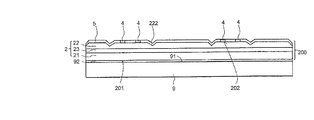
図1では、基板9が用意される。基板9は、平坦な表面91を有する。基板9は、パターン表面91を備えることもある。基板9は、例えば、可視、赤外線、および/または紫外線のスペクトル範囲にある電磁放射に関して、放射透過性、特に、透明なものである。あるいは、基板9は、放射不透過性のものとすることができる。基板9は、窒化ガリウム、または炭化ケイ素、またはサファイアを含み得る。基板9は、特に、シリコン基板となる。
In FIG. 1, a
半導体積層体200が、基板9の表面91の上に設けられる。半導体積層体200は、第1の半導体層21、第2の半導体層22、および第1の半導体層21と第2の半導体層22の間に配置される活性領域23を備える。第1の半導体層21はn伝導層とすることができ、第2の半導体層22はp伝導層とすることができる。この逆とすることも可能である。活性領域23は、例えば、電磁放射を発生させるように、または電磁放射を電気信号もしくはエネルギに吸収させ変換するように構成される。
The
半導体積層体200は、基板9の上にエピタキシャル成長させてよい。半導体積層体200は、基板9に面する第1の主表面201と、基板9から離れた第2の主表面202とを有する。半導体積層体200というエピタキシャル半導体層の品質を向上させるために、基板9は、パターン表面91を有してもよい。さらに、半導体積層体200は、第1の主表面201が基板9のパターン表面91を再現できるように、パターン表面91の上に成長させてもよい。
The
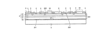
ミラー層3が、基板9から離れた第2の主表面202の上に堆積される。ミラー層3は、互いが横方向に離間した、複数の小領域を備える。特に、ミラー層3は、複数の開口部30を備える。ミラー層3の各小領域は、例えば、ミラー層3の開口部30を少なくとも1つは備える、連続したものであってよい。
A
ミラー層3は、特に、導電性のものとなる。平面視において、ミラー層3は、例えば、同じく導電性である、連絡層4によって覆われる。ミラー層3および/または連絡層4には、アルミニウム、ロジウム、パラジウム、銀、金、またはプラチナなどの金属、またはこれらの元素の合金が含有されてよい。
The
図2では、例えば、窒化ケイ素層または酸化ケイ素層である誘電層5が、半導体積層体200の上に設けられる。このとき、誘電層5が、連絡層4と、特に半導体積層体200とを、完全に覆う。
In FIG. 2, a
図3では、複数の凹部24が、ミラー層3の開口部30の領域に形成される。垂直方向において、各凹部24は、誘電層5、第2の半導体層22、活性領域23を貫通するように延び、第1の半導体層21にまで達する。凹部24は、半導体積層体200に有底穴を形成する。このとき、横方向において、凹部24は、半導体積層体200により、例えば完全に囲繞される。凹部24は、エッチング法(例えば、ドライエッチング法)によって形成され得る。
In FIG. 3, a plurality of
凹部24の形成後、例えば、SiO2などの酸化ケイ素層または窒化ケイ素層である不活性化層61が、凹部24の垂直面を覆うように形成される。不活性化層61は、凹部24および誘電層5を完全に覆うことが可能である。後続のステップにおいて、不活性化層61は、部分的に除去され得る。不活性化層61および誘電層5は、異なる誘電材料で構成されることが好ましい。一例として、誘電層5は窒化ケイ素を含有するか主成分とし、不活性化層61は酸化ケイ素を含有するか主成分とする。
After the formation of the
図4では、第1の半導体層21が凹部24の領域において露出するように、不活性化層61が、例えばエッチングによって部分的に除去される。不活性化層61を部分的に除去することにより、誘電層5も、少なくとも部分的に露出する。次のステップにおいて、誘電層5は、例えばエッチングにより、所々で除去される。その結果、誘電層5は、凹部24の領域における第1の開口部51に加え、凹部24の横方向に配置される複数の第2の開口部52を備える。第2の開口部52では、連絡層4などの導電層が、部分的に露出する。
In FIG. 4, the
図5では、第1の接触域71と、第2の接触域72と、バイア70とを備える接触構造7が、半導体積層体200の第2の主表面202の側に形成される。第1の接触域71および第2の接触域72は横方向に離間しており、このようにすることで、互いが電気的に絶縁する。垂直方向において、第2の接触域72は、誘電層5の第2の開口部52を貫通して延びており、ミラー層3および連絡層4により、第2の半導体層22に電気的に接続される。第1の接触域71は、凹部24の外側に堆積され、凹部24の内部に配置されたバイア70に電気的に接続される。垂直方向において、バイア70は、少なくとも第2の主表面202から、第2の半導体層22および活性領域23を貫通するように延び、第1の半導体層21にまで達する。凹部24の中では、横方向において、バイア70は、凹部24の垂直面を覆う不活性化層61により、第2の半導体層22および活性領域23から電気的に絶縁される。
In FIG. 5, a
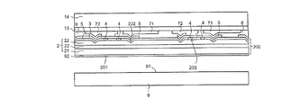
図6では、絶縁層6が、半導体積層体200の第2の主表面202の側に形成される。一例として、絶縁層6は、まず接触構造7を完全に覆う。後続のステップにおいて、絶縁層6は、略平坦な、特に、略平面な接続面67が形成されるように平面化することができる。図6での接続面67は、例えば、第1の接触域71および第2の接触域72の表面と、半導体積層体200から離れた絶縁層6の表面とによって形成される。換言すれば、平面化が施された後、垂直方向において、絶縁層6の表面は、特に、第1の接触域71および第2の接触域72の表面と同一の高さになる。接続面67において、第1の接触域71および第2の接触域72は部分的に露出する。凹部24と、ミラー層3の小領域間の領域との外側では、接続面67が平らな接続面として形成されることが好ましい。絶縁層6が凹部24を完全に埋めてもよい。
In FIG. 6, the insulating
図7では、補助基板14が、接続層13によって半導体積層体200に一時的に固定される。その結果、半導体積層体200は、補助基板14と基板9の間に配置される。補助基板14は、ポリマを含み得るか、ポリマ製のものとなる。接続層13は、スピンコーティング法によって接続面67に塗布することのできる接合材を含み得る。例えば、接続層13は、補助基板14を半導体積層体200に一時的に接合し、適時に半導体積層体200から補助基板14を解放するスピンオン接合材を含有する。接続層13は、例えば、温度依存性の粘着力を有する熱分解性のスピンオン接合材を含む。一例として、waferBOND(登録商標)処理(Brewer Science(登録商標))を利用すれば、補助基板14を半導体積層体200に一時的に接合し、その後、管理可能な時間を経た後で、補助基板14が勝手に剥離するようにすることが可能である。
In FIG. 7, the
接続層13には、他の好適な材料を使用することも可能である。例えば、接続層13は、フォトレジスト材料から形成されてよい。フォトレジスト材料(特に、ポジ型フォトレジスト材料)を使用することにより、接続層13は、例えばフォトリソグラフィ工程により、単純な方法で溶解させることができる。この場合、補助基板14は、放射透過性の材料から形成され得る。それにより、フォトレジスト材料を含む接続層13を、補助基板14を通過する放射に曝すことが可能となる。補助基板14の接続層13から離れた側に、保護層15が形成されることが好ましい。保護層15は、例えば放射不透過性であり、接続層13内のフォトレジスト材料の露出前に除去されてよい。例えば、保護層15は、Kapton(登録商標)層となる。
Other suitable materials can also be used for the
図8では、基板9が、半導体積層体200から切り離される。この切り離しは、例えば、機械的、化学的、または物理的な処理によってなされてよい。例えば、エッチング(特に、ドライエッチング)、研削、またはレーザ分離処理(レーザリフトオフ処理など)を利用することが可能である。基板除去のために、研削とエッチングを組み合わせて利用してもよい。
In FIG. 8, the
図9Aでは、半導体積層体200が横方向に構造化されて、複数の半導体本体2となる。横方向に構造化するということは、半導体積層体200が、互いが横方向に間隔を有する複数の半導体本体2へと分割されることを意味する。メサトレンチ20、または複数のトレンチ20が、半導体本体2の間に形成される。垂直方向において、トレンチ20は、半導体積層体200を貫通し、接続層13にまで延びる。トレンチ20は、エッチング法により(例えば、ドライエッチング法、ウェットエッチング法、またはレーザエッチング法により)、特に、ミラー層3の小領域間の領域において形成され得る。トレンチ20は、半導体積層体200から側方に形成されてもよい。半導体積層体200を複数の半導体本体2へと構造化するステップは、補助基板14を固定し、基板9を除去する処理の前に行うことも可能である。
In FIG. 9A, the
図9Aでは、半導体本体2の第1の主表面201にパターンが形成され、その結果、最適な光抽出面201となる。トレンチ20の形成および第1の主表面201のパターン形成は、共通の処理ステップで実現することも、直に続く2つのステップで実現することも可能である。とりわけ、トレンチ20を形成するステップは、半導体積層体200の第1の主表面201にパターンを形成するステップに続くものとなる。
In FIG. 9A, a pattern is formed on the first
図9Bに描かれた製造ステップは、実質的に、図9Aに描かれた製造ステップに相当するものである。図9Aと対照的なのは、基板9がパターン表面91を有しており、その上に半導体積層体200が設けられるということである。この場合、半導体積層体200は、パターンが形成された、特に、基板9のパターン表面91を再現した第1の主表面201を備える。基板9を除去し、半導体積層体200を構造化した後、各半導体本体2は、パターン形成された第1の主表面201を備えたものとなる。
The fabrication steps depicted in FIG. 9B substantially correspond to the fabrication steps depicted in FIG. 9A. In contrast to FIG. 9A, the
図10では、補助基板14がトレンチ20の領域において露出するように、接続層13が部分的に除去される。トレンチ20の領域の接続層13は、例えば、エッチング法やフォトリソグラフィ工程により、溶媒を用いて除去することができる。その結果、保護層15が部分的または完全に除去され得る。
In FIG. 10, the
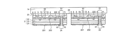
図11では、固着層8が、例えばコーティング法により、半導体本体2および補助基板14の上に設けられる。このとき、固着層8は、半導体本体2の垂直面と、半導体本体2の側方に配置された1つまたは複数のトレンチ20とを覆う。固着層8は、半導体本体2を補助基板に固定する。固着層8は、補助基板14と直接物理的に接触することが好ましい。図11に示すように、固着層8は、半導体本体2の垂直面および/または第1の主表面201を完全に覆うことができる。補助基板14を、半導体本体2に面するパターン表面(図示なし)を持たせて形成することが可能である。この場合、固着層8は、パターンが形成された補助基板14に侵入することができるため、固着層8が最適な形で補助基板14に固着される。なぜなら、表面がパターン形成されることによって補助基板14と固着層8の境界面が拡大されており、かかるパターン表面の接着面積も増大しているからである。
In FIG. 11, an
固着層8は、酸化ケイ素もしくは窒化ケイ素などの誘電材料から、またはフォトレジスト材料から形成され得る。例えば、固着層8は、フォトレジスト材料を相当に含むか、フォトレジスト材料から成るものとなる。固着層8は、実質的に、低温(<220℃)の誘電体から形成することや、低温の誘電体およびフォトレジスト材料によって形成することも可能である。
The pinned
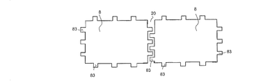
固着層8を設けた後、少なくとも、1つまたは複数のトレンチ20を覆う領域の固着層8を構造化することにより、複数のテザー83が形成される。テザー83は、特に、固着層8の一部を成すものであり、付随する半導体本体2の横方向に配置される。補助基板14を上面視した際、半導体本体2がテザー83と一切重なりを持たない場合もある。テザー83は、半導体本体2を補助基板14に機械的に固定するように形成される。固着層8を構造化するために、フォトリソグラフィ工程および/またはエッチング処理が利用され得る。
After providing the
図11Aでは、テザー83を備える固着層8が、補助基板14を平面視した状態で示されている。各半導体本体2の垂直面は、固着層8によって覆われている。固着層8は、異なる半導体本体2に付随する、横方向に離間した複数の固着層8へと構造化される。各半導体本体2は、その側面に、少なくとも1つまたは複数のテザー83を備える。固着層8は、異なる半導体本体2に付随するテザー83が切り離されるような形で、トレンチ20を覆う領域において構造化される。これにより、個々の半導体本体2を持ち上げる処理が単純化され、隣接する半導体本体2に影響を与えることはなくなる。
In FIG. 11A, the
図11Bでは、固着層8の別部分として、固着バー84が、半導体本体2の間に形成される。一例として、固着バー84は、横方向に沿って半導体本体2の列に沿って延在する。テザー83は、固着バー84に接続する。この場合、隣接する半導体本体2は、テザー83および固着バー84によって互いが機械的に接続されたものとなり得るため、複数の半導体本体2を、単純かつ安全な方法で同時に持ち上げることが可能となる。
In FIG. 11B, as another part of the
図12では、補助基板14が、半導体本体2から局部的に取り外される。しかし、半導体本体2は、テザー83により、間接的に補助基板14に接続されたままとなる。補助基板14の局部的な取り外しは、補助基板14と半導体本体2との間の機械的接続を、接続層13において溶解させることによって達成することができる。この作業は、例えば、時間経過による接続層13の溶媒剥離を利用するか、接続層13の接着効果を時間的に変化させることによって行われる。接続層13がフォトレジスト材料から形成される場合、接続層13は、補助基板14を透過可能な放射に曝すことによって溶解させることができる。テザー83を形成するステップおよび補助基板14を局部的に取り外すステップは、例えばフォトリソグラフィ工程により、共通の処理ステップで実現することが可能である。
In FIG. 12, the
図13では、半導体本体2の第1の主表面201側に、スタンプ82が取り付けられる。1つの第1の半導体層21と、1つの第2の半導体層22と、1つの活性領域23とを、バイア70を有する付随の接触構造7と併せ持つ半導体本体2は、テザー83が補助基板14から切り離されるような形で、スタンプ82によって選択的に拾い上げられ、補助基板14から持ち上げられてよい。例えば、テザー83は、機械的に破壊されるか、補助基板14から解放される。テザー83、または少なくともテザー83の何らかの残余物は、半導体本体2が完全に補助基板14から取り去られた後も、固着層8がテザー83、または少なくともテザー83の何らかの残余物を備えたままとなるような形で、補助基板14から取り外すことが可能である。複数の半導体本体2を、同時かつ選択的に拾い上げることも可能である。
In FIG. 13, the
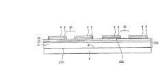
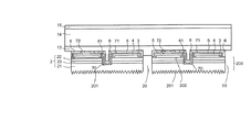
図14では、半導体本体2、ミラー層3、連絡層4、誘電層5、絶縁層6、不活性化層61、および接触構造7を有する本体210が、スタンプ82によって移送され、第1の接触パッド171と、絶縁パッド16によって第1の接触パッド171から横方向に離間された第2の接触パッド172とを有する支持体1に、機械的に接続される。支持体1は、例えば、第1の接触パッド171と、第2の接触パッド172と、絶縁パッド16との表面によって形成される、平らな接合面10を備える。本体210は、少なくとも凹部24の外側において、第1の接触域71と、第2の接触域72と、絶縁層6との表面によって形成される、平らな接続面67を備える。凹部24は、絶縁層6で完全に埋められてもよい。接合面10および接続面67は、例えばプラズマ洗浄方法により、表面仕上げされ、平面化されてよい。
In FIG. 14, the
特に、本体210および支持体1は、直接接合方法によって相互に接続される。この場合、接合面10が接続面67と直接接触することにより、本体210と支持体1の間に共通の境界面が形成される。このとき、共通の境界面は平らな表面であり、接着材は存在しない。共通の境界面は、特に、接続面67と接合面10の領域を直接重ねることによって形成される。特に、第1の接触域71および第2の接触域72は、それぞれ第1の接触パッド171および第2の接触パッド172と直接、電気的に接触する。例えば、共通の境界面は、金属と金属の境界面と、絶縁体と絶縁体の境界面と、金属と絶縁体の境界面とによって部分的に形成される(図15)。これとは対照的に、本体210を、接着材を用いる方法によって支持体1に接続することも可能である。
In particular, the
図15には、本明細書に記述される方法によって製造された、半導体部品100が示されている。接続面67と接合面10が直接重なり合う領域によって形成された共通の境界面において、第1の接触パッド171と合わさる第1の接触域71、および第2の接触パッド172と合わさる第2の接触域72は、いずれの場合も、垂直方向にステップ(すなわち、ジャンプ)を形成する。このことは、各接触域および各接触パッドが単一で共通の製造ステップではなく、異なる製造ステップにおいて形成され、直接接合方法によって相互に接続されることを示唆している。図15では、固着層8が、半導体部品100から完全に取り外される。特に、封止層が半導体本体2に設けられてよい。この封止層には、例えば、同封止層のマトリックス材料に埋め込まれた蛍光体粒子および/または散乱粒子が含まれる。固着層8は、放射透過性または放射透明な材料によって形成された場合、取り外す必要のないものとなり、半導体層部品100の封止層として機能し得る。
FIG. 15 shows a
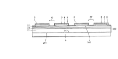
図16は、半導体部品100の別の例示的な実施形態を示す概略図である。この実施形態は、実質的に、図15の半導体部品100の実施形態に相当するものである。図15の実施形態と対照的なのは、垂直方向において、第1の接触パッド171および第2の接触パッド172が、接合面10から支持体1を貫通して基板の背面102にまで延びていることである。部品100は、例えば、背面102上の第1および第2の接触パッド171および172を通じて、外部電源へと電気的に接触させることが可能である。第1の主表面201は、放射通過領域101として、特に部品の放射出口領域として形成される。放射出口領域は、さらなる層によって保護されてもよい。
FIG. 16 is a schematic diagram illustrating another exemplary embodiment of the
図17Aから図17Hは、複数の半導体部品100を製造する方法に関する、いくつかの別のステップを示す図である。
17A-17H illustrate some additional steps in the method of fabricating a plurality of
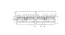
図17Aに描かれた製造ステップは、本質的に、図1で説明した製造ステップに相当するものである。対照的なのは、半導体積層体200には、基板9から離れた側にパターンが形成されており、その結果、半導体積層体200が有するパターン形成された第2の主表面202は、複数のマイクロプリズム222を備える形で形成されていることである。また、連絡層4が横方向に離間した複数の小領域を有しており、それらはいずれの場合も、誘電層を貫通して延び、第2の半導体層22と電気的に接触している。さらに、基板9と半導体層2との間に、中間層92が形成されている。中間層92は、エピタキシャル成長させる半導体本体2の品質を向上させることができる。特に、中間層92は、半導体本体2の半導体層のバンドギャップよりもバンドギャップが低い導電層となる。
The fabrication steps depicted in FIG. 17A essentially correspond to the fabrication steps described in FIG. In contrast, in the
図17Bでは、ミラー層3がパターン形成された第2の主表面202の上に設けられることにより、少なくとも所々で複数のマイクロプリズム222を形成している、パターン形成された第2の主表面202を、ミラー層3が再現する。ミラー層3は、連絡層4と電気的に接触する。絶縁層6にもパターンが形成される。
In FIG. 17B, the patterned second
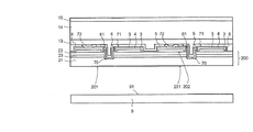
図17Cでは、接触構造7の第1の接触域71および第2の接触域72が、基板9から離れた半導体積層体200の側に形成される。このとき、平らな接続面67が、第1の接触域71と、第2の接触域72と、絶縁層6との表面によって形成される。平らな接続面67には、その全体にわたって凹凸が存在しない。
In FIG. 17C, the
図17Dおよび図17Eに描かれた製造ステップは、本質的に、図8から図10で説明した製造ステップに相当する。対照的なのは、凹部24およびバイア70が、基板9の取り外し後に形成されることである。垂直方向において、凹部24は、第1の主表面201から、半導体積層体200の全体を貫通し、第1の接触域71にまで延びる。バイア70は、第1の接触域71から第1の主表面201へと垂直方向に延び、特に、第1の主表面201において、第1の半導体層21と直接、電気的に接触する。
The fabrication steps depicted in FIGS. 17D and 17E essentially correspond to the fabrication steps described in FIGS. 8-10. In contrast, recesses 24 and vias 70 are formed after removal of
図17Fおよび図17Gに描かれた別の製造ステップは、本質的に、図12および図13で説明した製造ステップに相当する。ここでは、本体210のバイア70が、半導体本体2を貫通して延びている。本体210は、テザー83が機械的に破壊されるように、補助基板14から選択的に持ち上げることが可能である。このとき、テザー83、または少なくともテザー83の何らかの残余物は、補助基板14から取り外される。選択的に持ち上げられた本体210の固着層8は、補助基板14から完全に取り外された後も、テザー83、または少なくともテザー83の何らかの残余物を備える。
The additional manufacturing steps depicted in FIGS. 17F and 17G essentially correspond to the manufacturing steps described in FIGS. 12 and 13. Here, the
図17Hに描かれた製造ステップは、本質的に、図14で説明した製造ステップに相当するものである。対照的なのは、平らな接続面67に凹部24が存在しないことである。この場合、平らな接続面67には、特に、その全体にわたって凹凸が存在しない。
The fabrication steps depicted in FIG. 17H essentially correspond to the fabrication steps described in FIG. The contrast is the absence of the
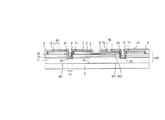
図17Iは、図17Gに描かれた本体210と、図16に描かれた支持体1とを備える、半導体部品100の例示的な別の実施形態を示す図である。この半導体部品100は支持体1の接合面10に配置された少なくとも1つのテザー83またはテザー83の残余物を有する固着層8を備える。固着層8は、半導体本体2の少なくとも1つの垂直面を覆う。このとき、テザー83、またはテザー83の残余物は、半導体本体2から側方に配置される。固着層8は、部分的または完全に取り外されてよい。特に、固着層8は、活性領域23によって放出された放射に対して放射透過性または放射透明な材料から形成され得る。この場合、支持体1から離れた固着層8の表面は、部品の放射出口領域101として形成されてよい。図17Iでは、凹部24が、固着層8によって完全には埋められない。固着層8の材料または別の材料により、凹部24を完全に埋めることも可能である。
FIG. 17I is a diagram showing another exemplary embodiment of a
半導体本体を補助基板に結合するためのテザーを、半導体本体を隔てるメサトレンチ内に形成する形で利用することにより、補助基板を取り外す処理の間、およびそれ以降、半導体本体を定位置に固定することができる。次いで、半導体本体を選択的に拾い上げ、支持体に直接接合することができる。このとき、支持体に対する半導体本体を電気的相互接続するための追加のステップは不要である。テザーを使用することにより、複数の半導体部品を製造する方法が単純化され、結果的に製造コストが抑えられる。 Fixing the semiconductor body in place during and after the process of removing the auxiliary substrate by utilizing a tether for coupling the semiconductor body to the auxiliary substrate in the form of a mesa trench separating the semiconductor body. Can. The semiconductor body can then be selectively picked up and bonded directly to the support. At this time, the additional step of electrically interconnecting the semiconductor body to the support is not necessary. The use of tethers simplifies the method of manufacturing multiple semiconductor components and consequently reduces manufacturing costs.
例示的な実施形態を参照しながら行った説明は、本発明をそれらの実施形態に限定するものではない。むしろ、本発明は、あらゆる新規の特徴と、特に請求項内の特徴のあらゆる組み合わせを含む、特徴の組み合わせの一切とを、たとえそれらの特徴またはそれらの組み合わせ自体が請求項または例示的な実施形態において明示されないものであったとしても、包含するものである。 The description given with reference to the exemplary embodiments does not limit the invention to these embodiments. Rather, the invention resides in any and all novel features, and in particular any combination of features, including any combination of features in the claims, even if the features or combinations thereof are themselves claim or example embodiments. Even if it is not specified in, it is included.
本出願は、米国特許出願第62/110,365号の優先権を主張するものであり、その開示内容は参照によって本明細書に組み込まれる。 This application claims priority to US Patent Application No. 62 / 110,365, the disclosure of which is incorporated herein by reference.
Claims (17)
前記本体(210)が、前記支持体(1)から離れた第1の主表面(201)と、前記支持体(1)に面する第2の主表面(202)とを有する半導体本体(2)を備え、
前記半導体本体(2)が、第1の半導体層(21)と、第2の半導体層(22)と、前記第1の半導体層と前記第2の半導体層との間に配置される活性領域(23)とを備え、
前記本体(210)が、前記第1の半導体層(21)と電気的に接触するために、前記第2の主表面(202)から、前記第2の半導体層(22)および前記活性領域(23)を貫通して延びるバイア(70)を有する接触構造(7)を備え、
前記接触構造(7)が、前記バイア(70)に電気的に接続された第1の接触域(71)と、第2の接触域(72)とを、前記第2の主表面(200)側に備え、
前記第1の接触域(71)および前記第2の接触域(72)が、絶縁層(6)によって横方向に離間され、
前記本体(210)が、前記第1の接触域(71)と、前記第2の接触域(72)と、前記絶縁層(6)との表面によって形成される、平らな接続面(67)を備え、
前記支持体(1)が、平らな接合面(10)を備え、前記接合面(10)が前記本体(210)の前記平らな接続面(67)と直接接触することにより、前記本体(210)と前記支持体(1)との間に共通の境界面が形成され、前記共通の境界面には、接着材またははんだ材が一切存在しない、
半導体部品。 A semiconductor component comprising a body (210) arranged on a support (1),
Semiconductor body (2) wherein said body (210) comprises a first major surface (201) remote from said support (1) and a second major surface (202) facing said support (1) Equipped with
An active region in which the semiconductor body (2) is disposed between a first semiconductor layer (21), a second semiconductor layer (22), and the first semiconductor layer and the second semiconductor layer And (23),
From the second major surface (202), the second semiconductor layer (22) and the active region (22) and the active region (22) for the body (210) to be in electrical contact with the first semiconductor layer (21). 23) comprising contact structures (7) with vias (70) extending through
A first contact area (71) electrically connected to the via (70) and a second contact area (72) by the contact structure (7); the second major surface (200) Prepare for the side,
Said first contact area (71) and said second contact area (72) being laterally separated by an insulating layer (6);
A flat connection surface (67), wherein said body (210) is formed by the surface of said first contact area (71), said second contact area (72) and said insulating layer (6). Equipped with
Said support (1) comprises a flat joint surface (10), said joint surface (10) being in direct contact with said flat connection surface (67) of said body (210), said body (210) A common interface between the support (1) and the support (1), wherein no adhesive or solder is present at the common interface,
Semiconductor parts.
前記平らな接合面(10)が、前記第1の接触パッド(171)と、前記第2の接触パッド(172)と、前記絶縁パッド(16)との表面によって形成され、
前記共通の境界面が、金属と金属の境界面と、絶縁体と絶縁体の境界面と、金属と絶縁体の境界面とによって部分的に形成される、
請求項1に記載の半導体部品。 The support (1) comprises a first contact pad (171) and a second contact pad (172) laterally spaced from the first contact pad (171) by an insulating pad (16). ,
The flat bonding surface (10) is formed by the surfaces of the first contact pad (171), the second contact pad (172) and the insulating pad (16).
The common interface is partially formed by a metal-to-metal interface, an insulator-to-insulator interface, and a metal-to-insulator interface.
The semiconductor component according to claim 1.
前記第1の接触域(71)および前記第2の接触域(72)はそれぞれ、前記第1の接触パッド(171)および前記第2の接触パッド(172)に直接、電気的に接触する、
請求項2に記載の半導体部品。 Said support (1) and said body (210) are fixed to each other at said common interface;
The first contact area (71) and the second contact area (72) are in direct electrical contact with the first contact pad (171) and the second contact pad (172), respectively
The semiconductor component according to claim 2.
請求項1〜3の何れか1項に記載の半導体部品。 The common interface is formed by the direct superposition of the flat connection surface (67) and the area of the flat connection surface (10) and is generally planar and without steps or edges.
The semiconductor component according to any one of claims 1 to 3.
請求項1〜4の何れか1項に記載の半導体部品。 The phosphor particles and / or scattering particles are embedded in a layer covering the first major surface (201),
The semiconductor component according to any one of claims 1 to 4.
ミラー層(3)が、前記第2の主表面(202)と前記支持体(1)との間に配置され、
前記ミラー層(3)が、少なくとも所々において、前記パターン形成された第2の主表面(202)を再現する、
請求項1〜5の何れか1項に記載の半導体部品。 The second major surface (202) is patterned and comprises a plurality of microprisms (222)
A mirror layer (3) is disposed between the second major surface (202) and the support (1);
The mirror layer (3) reproduces the patterned second major surface (202), at least in part.
The semiconductor component according to any one of claims 1 to 5.
前記絶縁層(6)の表面は、前記支持体(1)に面するように、前記第1の接触域(71)および前記第2の接触域(72)の表面と同一の高さにある、
請求項6に記載の半導体部品。 A pattern is formed on the insulating layer (6) facing away from the support (1).
The surface of the insulating layer (6) is at the same height as the surfaces of the first contact area (71) and the second contact area (72) so as to face the support (1). ,
The semiconductor component according to claim 6.
請求項1〜7の何れか1項に記載の半導体部品。 From the first main surface (201), through the whole of the semiconductor body (2) to a recess (24) extending to the first contact area (71);
The semiconductor component according to any one of claims 1 to 7.
請求項8に記載の半導体部品。 The via (70) is disposed in the recess (24) and extends vertically from the first contact area (71) to the first major surface (201), the first major surface ( Directly in electrical contact with the first semiconductor layer (21) at 201)
The semiconductor component according to claim 8.
前記バイア(70)は、前記凹部(24)の内側に配置され、前記第2の主表面(202)から前記第2の半導体層(22)および前記活性領域(23)を通って前記第1の半導体層(21)まで延びる、
請求項1〜7の何れか1項に記載の半導体部品。 The semiconductor body (2) is completely surrounded by the recess (24) forming a bottomed hole in the semiconductor body (2);
The via (70) is disposed inside the recess (24), and the first main surface (202) passes through the second semiconductor layer (22) and the active region (23). Extend to the semiconductor layer (21) of
The semiconductor component according to any one of claims 1 to 7.
請求項10に記載の半導体部品。 The first contact area (71) is deposited outside the recess (24) and electrically connected to the via (70).
The semiconductor component according to claim 10.
前記テザー(83)または前記テザー(83)の残部は、前記半導体本体(2)から側方に配置される、
請求項1〜11の何れか1項に記載の半導体部品。 Comprising an anchoring layer (8) comprising a residue of at least one tether (83) or tether (83) arranged on said joining surface (10) of said support (1);
The tether (83) or the remainder of the tether (83) is disposed laterally from the semiconductor body (2),
The semiconductor component according to any one of claims 1 to 11.
前記固着層(8)は、前記活性領域(23)によって放出された放射に対して放射透過性または放射透明な材料から形成され、
前記支持体(1)から離れた前記固着層(8)の表面は、部品の放射出口領域(101)を形成する、
請求項12に記載の半導体部品。 The vertical surface of the semiconductor body (2) is covered by the anchoring layer (8),
The anchoring layer (8) is formed of a material which is radiation transparent or radiation transparent to the radiation emitted by the active area (23).
The surface of the anchoring layer (8) remote from the support (1) forms the radiation exit area (101) of the part
The semiconductor component according to claim 12.
請求項12または13に記載の半導体部品。 The anchoring layer (8) is formed of a radiation-transparent or radiation-transparent material and functions as a sealing layer of the semiconductor component,
The semiconductor component according to claim 12 or 13.
前記本体(210)が、前記支持体(1)から離れた第1の主表面(201)と、前記支持体(1)に面する第2の主表面(202)とを有する半導体本体(2)を備え、
前記半導体本体(2)が、第1の半導体層(21)と、第2の半導体層(22)と、前記第1の半導体層と前記第2の半導体層との間に配置される活性領域(23)とを備え、
前記本体(210)が、前記第1の半導体層(21)と電気的に接触するために、前記第2の主表面(202)から、前記第2の半導体層(22)および前記活性領域(23)を貫通して延びるバイア(70)を有する接触構造(7)を備え、
前記接触構造(7)が、前記バイア(70)に電気的に接続された第1の接触域(71)と、第2の接触域(72)とを、前記第2の主表面(202)側に備え、
前記第1の接触域(71)および前記第2の接触域(72)が、絶縁層(6)によって横方向に離間され、
前記本体(210)が、前記第1の接触域(71)と、前記第2の接触域(72)と、前記絶縁層(6)との表面によって形成される、平らな接続面(67)を備え、
前記支持体(1)が、第1の接触パッド(171)と、絶縁パッド(16)によって前記第1の接触パッド(171)から横方向に離間した第2の接触パッド(172)とを備え、
前記支持体(1)が、が、前記第1の接触パッド(171)と、前記第2の接触パッド(172)と、前記絶縁パッド(16)との表面によって形成される平らな接合面(10)を備え、
前記支持体(1)および前記本体(210)は、接合材を用いて相互接続される、
半導体部品。 A semiconductor component comprising a body (210) arranged on a support (1),
Semiconductor body (2) wherein said body (210) comprises a first major surface (201) remote from said support (1) and a second major surface (202) facing said support (1) Equipped with
An active region in which the semiconductor body (2) is disposed between a first semiconductor layer (21), a second semiconductor layer (22), and the first semiconductor layer and the second semiconductor layer And (23),
From the second major surface (202), the second semiconductor layer (22) and the active region (22) and the active region (22) for the body (210) to be in electrical contact with the first semiconductor layer (21). 23) comprising contact structures (7) with vias (70) extending through
A first contact area (71) electrically connected to the via (70) and a second contact area (72) by the contact structure (7), the second major surface (202) Prepare for the side,
Said first contact area (71) and said second contact area (72) being laterally separated by an insulating layer (6);
A flat connection surface (67), wherein said body (210) is formed by the surface of said first contact area (71), said second contact area (72) and said insulating layer (6). Equipped with
The support (1) comprises a first contact pad (171) and a second contact pad (172) laterally spaced from the first contact pad (171) by an insulating pad (16). ,
Said support (1) is a flat bonding surface formed by the surface of said first contact pad (171), said second contact pad (172) and said insulating pad (16) 10),
The support (1) and the body (210) are interconnected using a bonding material
Semiconductor parts.
全ての前記半導体部品(100)の前記支持体(1)が、単一で共通な支持体として形成される、
デバイス。 A device comprising a plurality of semiconductor components (100) according to any one of the preceding claims, wherein
The supports (1) of all the semiconductor components (100) are formed as a single, common support
device.
請求項16に記載のデバイス。 Each of the semiconductor components (100) comprises a body (210) arranged in the form of a matrix with columns and rows on the single common support.
A device according to claim 16.
Applications Claiming Priority (2)
| Application Number | Priority Date | Filing Date | Title |
|---|---|---|---|
| US201562110365P | 2015-01-30 | 2015-01-30 | |
| US62/110,365 | 2015-01-30 |
Related Parent Applications (1)
| Application Number | Title | Priority Date | Filing Date |
|---|---|---|---|
| JP2017536551A Division JP6483841B2 (en) | 2015-01-30 | 2016-01-28 | Method, semiconductor component and device for manufacturing a semiconductor component |
Publications (2)
| Publication Number | Publication Date |
|---|---|
| JP2019096902A true JP2019096902A (en) | 2019-06-20 |
| JP6824307B2 JP6824307B2 (en) | 2021-02-03 |
Family
ID=55405301
Family Applications (2)
| Application Number | Title | Priority Date | Filing Date |
|---|---|---|---|
| JP2017536551A Active JP6483841B2 (en) | 2015-01-30 | 2016-01-28 | Method, semiconductor component and device for manufacturing a semiconductor component |
| JP2019024750A Active JP6824307B2 (en) | 2015-01-30 | 2019-02-14 | Methods for manufacturing semiconductor components and semiconductor components |
Family Applications Before (1)
| Application Number | Title | Priority Date | Filing Date |
|---|---|---|---|
| JP2017536551A Active JP6483841B2 (en) | 2015-01-30 | 2016-01-28 | Method, semiconductor component and device for manufacturing a semiconductor component |
Country Status (5)
| Country | Link |
|---|---|
| US (1) | US9773945B2 (en) |
| JP (2) | JP6483841B2 (en) |
| CN (1) | CN107210294B (en) |
| DE (1) | DE112016000533T5 (en) |
| WO (1) | WO2016120398A1 (en) |
Families Citing this family (11)
| Publication number | Priority date | Publication date | Assignee | Title |
|---|---|---|---|---|
| DE102014102029A1 (en) * | 2014-02-18 | 2015-08-20 | Osram Opto Semiconductors Gmbh | Process for the production of semiconductor devices and semiconductor device |
| JP6483841B2 (en) * | 2015-01-30 | 2019-03-13 | オスラム オプト セミコンダクターズ ゲゼルシャフト ミット ベシュレンクテル ハフツングOsram Opto Semiconductors GmbH | Method, semiconductor component and device for manufacturing a semiconductor component |
| DE102017106730A1 (en) | 2017-03-29 | 2018-10-04 | Osram Opto Semiconductors Gmbh | Method for producing a component and component for an electronic component |
| DE102017114467A1 (en) | 2017-06-29 | 2019-01-03 | Osram Opto Semiconductors Gmbh | Semiconductor chip with transparent current spreading layer |
| DE102017115794A1 (en) * | 2017-07-13 | 2019-01-17 | Osram Opto Semiconductors Gmbh | Optoelectronic component and method for producing an optoelectronic component |
| EP3591345B1 (en) * | 2018-07-02 | 2020-11-11 | Dr. Johannes Heidenhain GmbH | Position measuring device and method for producing a light source for a sensor unit of a position measuring device |
| EP3591346B1 (en) * | 2018-07-02 | 2020-11-11 | Dr. Johannes Heidenhain GmbH | Position measuring device and method for producing a light source for a sensor unit of a position measuring device |
| DE102019108701A1 (en) * | 2019-04-03 | 2020-10-08 | OSRAM Opto Semiconductors Gesellschaft mit beschränkter Haftung | Process for the production of a plurality of components, component and component composite from components |
| JP7364603B2 (en) | 2019-06-13 | 2023-10-18 | 京東方科技集團股▲ふん▼有限公司 | Mass transfer method and system for micro light emitting diode |
| US11038088B2 (en) | 2019-10-14 | 2021-06-15 | Lextar Electronics Corporation | Light emitting diode package |
| TWM643626U (en) * | 2020-09-30 | 2023-07-11 | 日商信越化學工業股份有限公司 | Laser-induced forward transfer system, laser-induced forward transfer device, optical element transferred acceptor substrate manufacturing system, and display manufacturing system |
Citations (9)
| Publication number | Priority date | Publication date | Assignee | Title |
|---|---|---|---|---|
| JP2007173579A (en) * | 2005-12-22 | 2007-07-05 | Matsushita Electric Works Ltd | Semiconductor light emitting device and its manufacturing method |
| US20100317132A1 (en) * | 2009-05-12 | 2010-12-16 | Rogers John A | Printed Assemblies of Ultrathin, Microscale Inorganic Light Emitting Diodes for Deformable and Semitransparent Displays |
| JP2011044643A (en) * | 2009-08-24 | 2011-03-03 | Oki Data Corp | Semiconductor light-emitting element array device, image exposure apparatus, image forming apparatus, and image display device |
| JP2012009901A (en) * | 2011-10-07 | 2012-01-12 | Oki Data Corp | Display device |
| JP2012019217A (en) * | 2010-07-08 | 2012-01-26 | Samsung Led Co Ltd | Semiconductor light-emitting device and method of manufacturing the same, illuminating device and backlight |
| JP2014090052A (en) * | 2012-10-30 | 2014-05-15 | Nichia Chem Ind Ltd | Light-emitting element, light-emitting device and light-emitting device manufacturing method |
| JP2014139999A (en) * | 2013-01-21 | 2014-07-31 | Toshiba Corp | Semiconductor light-emitting device |
| JP2014160736A (en) * | 2013-02-19 | 2014-09-04 | Toshiba Corp | Semiconductor light-emitting device and light-emitting device |
| JP6483841B2 (en) * | 2015-01-30 | 2019-03-13 | オスラム オプト セミコンダクターズ ゲゼルシャフト ミット ベシュレンクテル ハフツングOsram Opto Semiconductors GmbH | Method, semiconductor component and device for manufacturing a semiconductor component |
Family Cites Families (9)
| Publication number | Priority date | Publication date | Assignee | Title |
|---|---|---|---|---|
| US7576365B2 (en) * | 2004-03-12 | 2009-08-18 | Showa Denko K.K. | Group III nitride semiconductor light-emitting device, forming method thereof, lamp and light source using same |
| CN101517700B (en) | 2006-09-20 | 2014-04-16 | 伊利诺伊大学评议会 | Release strategies for making transferable semiconductor structures, devices and device components |
| DE102007019776A1 (en) | 2007-04-26 | 2008-10-30 | Osram Opto Semiconductors Gmbh | Optoelectronic component and method for producing a plurality of optoelectronic components |
| JP4381439B2 (en) * | 2007-09-18 | 2009-12-09 | 株式会社沖データ | LED backlight device and liquid crystal display device |
| WO2010111601A2 (en) | 2009-03-26 | 2010-09-30 | Semprius, Inc. | Methods of forming printable integrated circuit devices and devices formed thereby |
| DE102009056386A1 (en) * | 2009-11-30 | 2011-06-01 | Osram Opto Semiconductors Gmbh | Process for the production of semiconductor devices |
| DE102010013494A1 (en) * | 2010-03-31 | 2011-10-06 | Osram Opto Semiconductors Gmbh | Optoelectronic semiconductor chip |
| JP2014139998A (en) * | 2013-01-21 | 2014-07-31 | Toshiba Corp | Semiconductor light-emitting device |
| CN106716611B (en) * | 2014-10-17 | 2019-08-20 | 英特尔公司 | Micro- pickup and bonding assembling |
-
2016
- 2016-01-28 JP JP2017536551A patent/JP6483841B2/en active Active
- 2016-01-28 WO PCT/EP2016/051827 patent/WO2016120398A1/en active Application Filing
- 2016-01-28 DE DE112016000533.4T patent/DE112016000533T5/en active Granted
- 2016-01-28 US US15/009,736 patent/US9773945B2/en active Active
- 2016-01-28 CN CN201680007835.7A patent/CN107210294B/en active Active
-
2019
- 2019-02-14 JP JP2019024750A patent/JP6824307B2/en active Active
Patent Citations (9)
| Publication number | Priority date | Publication date | Assignee | Title |
|---|---|---|---|---|
| JP2007173579A (en) * | 2005-12-22 | 2007-07-05 | Matsushita Electric Works Ltd | Semiconductor light emitting device and its manufacturing method |
| US20100317132A1 (en) * | 2009-05-12 | 2010-12-16 | Rogers John A | Printed Assemblies of Ultrathin, Microscale Inorganic Light Emitting Diodes for Deformable and Semitransparent Displays |
| JP2011044643A (en) * | 2009-08-24 | 2011-03-03 | Oki Data Corp | Semiconductor light-emitting element array device, image exposure apparatus, image forming apparatus, and image display device |
| JP2012019217A (en) * | 2010-07-08 | 2012-01-26 | Samsung Led Co Ltd | Semiconductor light-emitting device and method of manufacturing the same, illuminating device and backlight |
| JP2012009901A (en) * | 2011-10-07 | 2012-01-12 | Oki Data Corp | Display device |
| JP2014090052A (en) * | 2012-10-30 | 2014-05-15 | Nichia Chem Ind Ltd | Light-emitting element, light-emitting device and light-emitting device manufacturing method |
| JP2014139999A (en) * | 2013-01-21 | 2014-07-31 | Toshiba Corp | Semiconductor light-emitting device |
| JP2014160736A (en) * | 2013-02-19 | 2014-09-04 | Toshiba Corp | Semiconductor light-emitting device and light-emitting device |
| JP6483841B2 (en) * | 2015-01-30 | 2019-03-13 | オスラム オプト セミコンダクターズ ゲゼルシャフト ミット ベシュレンクテル ハフツングOsram Opto Semiconductors GmbH | Method, semiconductor component and device for manufacturing a semiconductor component |
Also Published As
| Publication number | Publication date |
|---|---|
| JP6483841B2 (en) | 2019-03-13 |
| DE112016000533T5 (en) | 2017-10-19 |
| US20160225953A1 (en) | 2016-08-04 |
| CN107210294B (en) | 2020-03-03 |
| JP2018506850A (en) | 2018-03-08 |
| WO2016120398A1 (en) | 2016-08-04 |
| JP6824307B2 (en) | 2021-02-03 |
| CN107210294A (en) | 2017-09-26 |
| US9773945B2 (en) | 2017-09-26 |
Similar Documents
| Publication | Publication Date | Title |
|---|---|---|
| JP2019096902A (en) | Method for manufacturing semiconductor component and semiconductor component | |
| JP6544730B2 (en) | Method and semiconductor component for manufacturing semiconductor component | |
| US10892384B2 (en) | Etched trenches in bond materials for die singulation, and associated systems and methods | |
| JP6262745B2 (en) | Light emitting diode display manufacturing method and light emitting diode display | |
| US8604491B2 (en) | Wafer level photonic device die structure and method of making the same | |
| US8236584B1 (en) | Method of forming a light emitting diode emitter substrate with highly reflective metal bonding | |
| CN106537616B (en) | Light emitting device | |
| US20110198609A1 (en) | Light-Emitting Devices with Through-Substrate Via Connections | |
| US20170069804A1 (en) | Method for manufacturing light emitting device | |
| JP5964970B2 (en) | Discontinuous patterned bonding and related systems and methods for semiconductor devices | |
| JP2014523632A (en) | Semiconductor wafer bonding incorporating electrical and optical interconnects | |
| EP2438625B1 (en) | Method of forming a dielectric layer on a semiconductor light emitting device, and semiconductor light emitting device with a dielectric layer | |
| JP6470677B2 (en) | Encapsulated semiconductor light emitting device | |
| US8598611B2 (en) | Vertical solid-state transducers and solid-state transducer arrays having backside terminals and associated systems and methods | |
| WO2014120086A1 (en) | Method of fabricating semiconductor devices | |
| US11107944B2 (en) | Method of manufacturing an optoelectronic semiconductor chip and optoelectronic semiconductor chip | |
| WO2014106306A1 (en) | High-voltage flip chip led structure and manufacturing method therefor | |
| JP5834109B2 (en) | Semiconductor light emitting device, method for manufacturing semiconductor light emitting device, and method for manufacturing light emitting device | |
| WO2013057668A1 (en) | Led wafer bonded to carrier wafer for wafer level processing | |
| US20240097087A1 (en) | Method of Transferring Patterned Micro-LED Die onto a Silicon Carrier for Wafer-to-Wafer Hybrid Bonding to a CMOS Backplane | |
| US20160343924A1 (en) | LED-Based Light Emitting Devices Having Metal Spacer Layers |
Legal Events
| Date | Code | Title | Description |
|---|---|---|---|
| A621 | Written request for application examination |
Free format text: JAPANESE INTERMEDIATE CODE: A621 Effective date: 20190214 |
|
| RD02 | Notification of acceptance of power of attorney |
Free format text: JAPANESE INTERMEDIATE CODE: A7422 Effective date: 20190703 |
|
| RD04 | Notification of resignation of power of attorney |
Free format text: JAPANESE INTERMEDIATE CODE: A7424 Effective date: 20190708 |
|
| A131 | Notification of reasons for refusal |
Free format text: JAPANESE INTERMEDIATE CODE: A131 Effective date: 20191119 |
|
| A521 | Request for written amendment filed |
Free format text: JAPANESE INTERMEDIATE CODE: A523 Effective date: 20200204 |
|
| A131 | Notification of reasons for refusal |
Free format text: JAPANESE INTERMEDIATE CODE: A131 Effective date: 20200602 |
|
| A521 | Request for written amendment filed |
Free format text: JAPANESE INTERMEDIATE CODE: A523 Effective date: 20200824 |
|
| TRDD | Decision of grant or rejection written | ||
| A01 | Written decision to grant a patent or to grant a registration (utility model) |
Free format text: JAPANESE INTERMEDIATE CODE: A01 Effective date: 20201215 |
|
| A61 | First payment of annual fees (during grant procedure) |
Free format text: JAPANESE INTERMEDIATE CODE: A61 Effective date: 20210112 |
|
| R150 | Certificate of patent or registration of utility model |
Ref document number: 6824307 Country of ref document: JP Free format text: JAPANESE INTERMEDIATE CODE: R150 |
|
| R250 | Receipt of annual fees |
Free format text: JAPANESE INTERMEDIATE CODE: R250 |