JP2018091888A - Optical receptacle, optical module, and manufacturing method of optical module - Google Patents

Optical receptacle, optical module, and manufacturing method of optical module Download PDF

Info

Publication number
JP2018091888A
JP2018091888A JP2016232527A JP2016232527A JP2018091888A JP 2018091888 A JP2018091888 A JP 2018091888A JP 2016232527 A JP2016232527 A JP 2016232527A JP 2016232527 A JP2016232527 A JP 2016232527A JP 2018091888 A JP2018091888 A JP 2018091888A
Authority
JP
Japan
Prior art keywords
optical
optical receptacle
contact surface
bonding
support member
Prior art date
Legal status (The legal status is an assumption and is not a legal conclusion. Google has not performed a legal analysis and makes no representation as to the accuracy of the status listed.)
Ceased
Application number
JP2016232527A
Other languages
Japanese (ja)
Inventor
心平 森岡
Shinpei Morioka
心平 森岡
崇文 國谷
Takafumi Kunitani
崇文 國谷
Current Assignee (The listed assignees may be inaccurate. Google has not performed a legal analysis and makes no representation or warranty as to the accuracy of the list.)
Enplas Corp
Original Assignee
Enplas Corp
Priority date (The priority date is an assumption and is not a legal conclusion. Google has not performed a legal analysis and makes no representation as to the accuracy of the date listed.)
Filing date
Publication date
Application filed by Enplas Corp filed Critical Enplas Corp
Priority to JP2016232527A priority Critical patent/JP2018091888A/en
Priority to PCT/JP2017/041937 priority patent/WO2018101137A1/en
Priority to CN201780073695.8A priority patent/CN110023806A/en
Priority to US16/465,194 priority patent/US10627586B2/en
Publication of JP2018091888A publication Critical patent/JP2018091888A/en
Ceased legal-status Critical Current

Links

Images

Classifications

    • GPHYSICS
    • G02OPTICS
    • G02BOPTICAL ELEMENTS, SYSTEMS OR APPARATUS
    • G02B6/00Light guides; Structural details of arrangements comprising light guides and other optical elements, e.g. couplings
    • G02B6/24Coupling light guides
    • G02B6/42Coupling light guides with opto-electronic elements
    • G02B6/4201Packages, e.g. shape, construction, internal or external details
    • G02B6/4204Packages, e.g. shape, construction, internal or external details the coupling comprising intermediate optical elements, e.g. lenses, holograms
    • G02B6/4206Optical features
    • GPHYSICS
    • G02OPTICS
    • G02BOPTICAL ELEMENTS, SYSTEMS OR APPARATUS
    • G02B6/00Light guides; Structural details of arrangements comprising light guides and other optical elements, e.g. couplings
    • G02B6/24Coupling light guides
    • G02B6/42Coupling light guides with opto-electronic elements
    • G02B6/4201Packages, e.g. shape, construction, internal or external details
    • G02B6/4204Packages, e.g. shape, construction, internal or external details the coupling comprising intermediate optical elements, e.g. lenses, holograms
    • G02B6/4214Packages, e.g. shape, construction, internal or external details the coupling comprising intermediate optical elements, e.g. lenses, holograms the intermediate optical element having redirecting reflective means, e.g. mirrors, prisms for deflecting the radiation from horizontal to down- or upward direction toward a device
    • GPHYSICS
    • G02OPTICS
    • G02BOPTICAL ELEMENTS, SYSTEMS OR APPARATUS
    • G02B6/00Light guides; Structural details of arrangements comprising light guides and other optical elements, e.g. couplings
    • G02B6/24Coupling light guides
    • G02B6/42Coupling light guides with opto-electronic elements
    • G02B6/4201Packages, e.g. shape, construction, internal or external details
    • G02B6/4219Mechanical fixtures for holding or positioning the elements relative to each other in the couplings; Alignment methods for the elements, e.g. measuring or observing methods especially used therefor
    • G02B6/4236Fixing or mounting methods of the aligned elements
    • G02B6/4239Adhesive bonding; Encapsulation with polymer material
    • GPHYSICS
    • G02OPTICS
    • G02BOPTICAL ELEMENTS, SYSTEMS OR APPARATUS
    • G02B6/00Light guides; Structural details of arrangements comprising light guides and other optical elements, e.g. couplings
    • G02B6/24Coupling light guides
    • G02B6/42Coupling light guides with opto-electronic elements
    • G02B6/4201Packages, e.g. shape, construction, internal or external details
    • G02B6/4246Bidirectionally operating package structures
    • GPHYSICS
    • G02OPTICS
    • G02BOPTICAL ELEMENTS, SYSTEMS OR APPARATUS
    • G02B6/00Light guides; Structural details of arrangements comprising light guides and other optical elements, e.g. couplings
    • G02B6/24Coupling light guides
    • G02B6/42Coupling light guides with opto-electronic elements
    • G02B6/4292Coupling light guides with opto-electronic elements the light guide being disconnectable from the opto-electronic element, e.g. mutually self aligning arrangements
    • GPHYSICS
    • G02OPTICS
    • G02BOPTICAL ELEMENTS, SYSTEMS OR APPARATUS
    • G02B6/00Light guides; Structural details of arrangements comprising light guides and other optical elements, e.g. couplings
    • G02B6/24Coupling light guides
    • G02B6/36Mechanical coupling means
    • G02B6/38Mechanical coupling means having fibre to fibre mating means
    • G02B6/3807Dismountable connectors, i.e. comprising plugs
    • G02B6/3873Connectors using guide surfaces for aligning ferrule ends, e.g. tubes, sleeves, V-grooves, rods, pins, balls
    • G02B6/3885Multicore or multichannel optical connectors, i.e. one single ferrule containing more than one fibre, e.g. ribbon type

Landscapes

  • Physics & Mathematics (AREA)
  • General Physics & Mathematics (AREA)
  • Optics & Photonics (AREA)
  • Optical Couplings Of Light Guides (AREA)

Abstract

PROBLEM TO BE SOLVED: To improve the degree of design freedom by securing on a substrate an area for wire bonding and an area for arranging other optical components and electronic components, and to suppress displacement of the position of an optical receptacle due to stress generated when an optical transmission body is attached and detached.SOLUTION: The optical receptacle has an optical receptacle body and a bearing member. The optical receptacle body contacts the bearing member on a first contact surface, a second contact surface and a third contact surface. The bearing member includes a second engagement part engaging with a first engagement part arranged on the first contact surface of the optical receptacle body. With being separated from a virtual plane including an installation surface of the bearing member, the optical receptacle body is attached to the bearing member through adhesive arranged in an adhesive open hole of the optical receptacle body and in an adhesive recess of the bearing member. The adhesive open hole opens to the third contact surface of the optical receptacle body and a surface thereof opposite the third contact surface.SELECTED DRAWING: Figure 1

Description

本発明は、光レセプタクル、当該光レセプタクルを有する光モジュール、および当該光モジュールの製造方法に関する。   The present invention relates to an optical receptacle, an optical module having the optical receptacle, and a method for manufacturing the optical module.

従来、光ファイバーや光導波路などの光伝送体を用いた光通信には、面発光レーザー(例えば、VCSEL:Vertical Cavity Surface Emitting Laser)などの発光素子(以下、「光素子」ともいう)を備えた光モジュールが使用されている。光モジュールは、発光素子から出射された通信情報を含む光を、光伝送体に入射させる光レセプタクル(以下、「光ソケット」ともいう)を有する(例えば、特許文献1参照)。   Conventionally, optical communication using an optical transmission body such as an optical fiber or an optical waveguide has been provided with a light emitting element (hereinafter also referred to as an “optical element”) such as a surface emitting laser (for example, VCSEL: Vertical Cavity Surface Emitting Laser). An optical module is used. The optical module has an optical receptacle (hereinafter also referred to as “optical socket”) that allows light including communication information emitted from the light emitting element to enter the optical transmission body (see, for example, Patent Document 1).

特許文献1に記載の光モジュールは、透明基板と、透明基板の一方の面に配置され、光素子と光伝送体の端面とを光学的に結合するための光ソケットと、透明基板の他方の面であって、光ソケットに対応する位置に配置された光素子と、を有する。光ソケットおよび光素子は、透明基板に直接接着されている。光ソケットには、光伝送体の一端部に設けられた光プラグが取り付けられる。特許文献1に記載の光モジュールでは、光素子の発光面は透明基板に対向しているため、当該発光面の破損や、当該発光面に対する異物の付着などの不具合を抑制することができる。   The optical module described in Patent Document 1 is arranged on a transparent substrate, one surface of the transparent substrate, an optical socket for optically coupling the optical element and the end surface of the optical transmission body, and the other of the transparent substrate. And an optical element disposed at a position corresponding to the optical socket. The optical socket and the optical element are directly bonded to the transparent substrate. An optical plug provided at one end of the optical transmission body is attached to the optical socket. In the optical module described in Patent Document 1, since the light emitting surface of the optical element faces the transparent substrate, problems such as breakage of the light emitting surface and adhesion of foreign matters to the light emitting surface can be suppressed.

特開2004−246279号公報JP 2004-246279 A

しかしながら、特許文献1に記載の光モジュールでは、光ソケットが基板に直接接着されているため、当該基板上において、ワイヤーボンディングのための領域、および他の光学部品や電子部品などを配置するための領域が制限されるという問題がある。光伝送体の一端部に設けられた光プラグは、光ソケットに直接取り付けられるため、光伝送体の着脱時、および光モジュールの使用時に生じる応力が、光プラグを介して光ソケットに伝達しうる。この結果として、光ソケットの位置がずれたり、光ソケットが外れたりするという問題もある。   However, in the optical module described in Patent Document 1, since the optical socket is directly bonded to the substrate, the region for wire bonding and other optical components and electronic components are arranged on the substrate. There is a problem that the area is limited. Since the optical plug provided at one end of the optical transmission body is directly attached to the optical socket, the stress generated when the optical transmission body is attached or detached and when the optical module is used can be transmitted to the optical socket through the optical plug. . As a result, there is a problem that the position of the optical socket is shifted or the optical socket is detached.

本発明の目的は、基板上において、ワイヤーボンディングのための領域、および他の光学部品や電子部品などを配置するための領域を確保することで設計の自由度をより高め、かつ光伝送体の着脱時、および光モジュールの使用時に生じる応力によって、光レセプタクル本体の位置がずれたり、光レセプタクル本体が外れたりし難くすることである。   An object of the present invention is to increase the degree of freedom of design by securing a region for wire bonding and a region for arranging other optical components and electronic components on a substrate, and for an optical transmission body. This is to make it difficult for the position of the optical receptacle body to be displaced or to be removed from the optical receptacle body due to the stress generated when the optical module is attached or detached and when the optical module is used.

本発明に係る光レセプタクルは、基板上に光電変換素子が配置された光電変換装置と、光伝送体との間に配置され、前記光電変換素子と前記光伝送体の端面とを光学的に結合するための光レセプタクルであって、前記光伝送体の端面に対向する面側から順に配置されている、第1当接面、第2当接面および第3当接面を含む光レセプタクル本体と、前記第1当接面、前記第2当接面および前記第3当接面に当接した状態で、前記光レセプタクル本体を支持している支持部材と、を有し、前記光レセプタクル本体は、前記光電変換素子から出射された送信光を入射させるか、または前記光伝送体の端面から出射され、前記光レセプタクル本体の内部を通った受信光を前記光電変換素子に向けて出射させる第1光学面と、前記光電変換素子から出射され、前記光レセプタクル本体の内部を通った前記送信光を前記光伝送体に向けて出射させるか、または前記光伝送体から出射された前記受信光を入射させる第2光学面と、前記第1光学面で入射した前記送信光を前記第2光学面に向けて反射させるか、または前記第2光学面で入射した前記受信光を前記第1光学面に向けて反射させる反射面と、前記第1当接面に配置されている第1嵌合部と、前記第3当接面と、前記第3当接面の反対側に位置している面とに開口している接着用貫通孔と、を有し、前記第1当接面および前記第3当接面は、前記第1光学面が配置された面の反対側に配置され、前記第2当接面は、前記第2光学面が配置された面の反対側に配置され、前記支持部材は、前記基板に設置されるための設置面と、前記第1当接面に対向する面に配置され、前記第1嵌合部に嵌合されている第2嵌合部と、前記第3当接面に対向する面に開口し、かつ前記接着用貫通孔に連通している接着用凹部と、を有し、前記光レセプタクル本体は、前記設置面を含む仮想平面と離間した状態で、前記接着用貫通孔および前記接着用凹部の内部に配置されている接着剤を介して、前記支持部材に接着されている。   An optical receptacle according to the present invention is disposed between a photoelectric conversion device having a photoelectric conversion element disposed on a substrate and an optical transmission body, and optically couples the photoelectric conversion element and an end face of the optical transmission body. An optical receptacle main body including a first contact surface, a second contact surface, and a third contact surface, which are disposed in order from the surface facing the end surface of the optical transmission body. A support member that supports the optical receptacle body in a state of being in contact with the first contact surface, the second contact surface, and the third contact surface, wherein the optical receptacle body is First, the transmission light emitted from the photoelectric conversion element is incident, or the reception light emitted from the end face of the optical transmission body and passing through the inside of the optical receptacle body is emitted toward the photoelectric conversion element. The optical surface and the photoelectric conversion element A second optical surface that emits the transmission light that has passed through the inside of the optical receptacle main body toward the optical transmission body, or that receives the reception light emitted from the optical transmission body, and the first optical surface. A reflection surface that reflects the transmission light incident on the optical surface toward the second optical surface, or reflects the reception light incident on the second optical surface toward the first optical surface; A bonding through-hole opened to a first fitting portion disposed on one contact surface, the third contact surface, and a surface located on the opposite side of the third contact surface; The first contact surface and the third contact surface are disposed on the opposite side of the surface on which the first optical surface is disposed, and the second contact surface is the second optical surface. Is disposed on the opposite side of the surface on which the support member is disposed, the support member is disposed on the substrate, and the first surface is disposed on the substrate. A second fitting portion that is disposed on a surface that faces the contact surface, is fitted to the first fitting portion, and is open to a surface that faces the third contact surface. A bonding recess that is in communication, and the optical receptacle body is disposed inside the bonding through-hole and the bonding recess in a state of being separated from a virtual plane including the installation surface. It is bonded to the support member via an agent.

本発明に係る光モジュールは、基板および前記基板上に配置されている光電変換素子を含む光電変換装置と、本発明に係る光レセプタクルと、を有し、前記基板および前記光レセプタクル本体は互いに離間している。   An optical module according to the present invention includes a substrate, a photoelectric conversion device including a photoelectric conversion element disposed on the substrate, and an optical receptacle according to the present invention, and the substrate and the optical receptacle body are separated from each other. doing.

本発明に係る光モジュールの製造方法は、前記第1当接面、前記第2当接面および前記第3当接面で、前記光レセプタクル本体を前記支持部材に当接させた状態で、前記接着用貫通孔および前記接着用凹部の内部に接着剤を注入し、硬化させることで、前記光レセプタクル本体および前記支持部材を互いに接着する工程と、前記基板および前記光レセプタクル本体が互いに離間した状態で、前記光レセプタクルおよび前記基板を互いに固定する工程と、を含む。   The method of manufacturing an optical module according to the present invention includes the first contact surface, the second contact surface, and the third contact surface, wherein the optical receptacle body is in contact with the support member, A step of bonding the optical receptacle body and the support member to each other by injecting an adhesive into the bonding through-hole and the bonding recess, and curing the adhesive; and a state where the substrate and the optical receptacle body are separated from each other And fixing the optical receptacle and the substrate to each other.

本発明によれば、基板上において、ワイヤーボンディングのための領域、および他の光学部品や電子部品などを配置するための領域を確保することで設計の自由度をより高めることができ、かつ光伝送体の着脱時および光モジュールの使用時に生じる応力によって、光レセプタクル本体の位置がずれたり、光レセプタクル本体が外れたりし難くすることができる。   According to the present invention, it is possible to further increase the degree of freedom of design by securing an area for wire bonding and an area for arranging other optical components and electronic components on the substrate, and light. It is possible to make it difficult for the position of the optical receptacle body to shift or to remove the optical receptacle body due to stress generated when the transmission body is attached or detached and when the optical module is used.

図1は、実施の形態1に係る光モジュールの構成を模式的に示す側面図である。FIG. 1 is a side view schematically showing the configuration of the optical module according to Embodiment 1. FIG. 図2A〜Dは、実施の形態1に係る光レセプタクル本体の構成を示す図である。2A to 2D are diagrams showing the configuration of the optical receptacle body according to Embodiment 1. FIG. 図3A〜Dは、実施の形態1に係る支持部材の構成を示す図である。3A to 3D are diagrams illustrating the configuration of the support member according to the first embodiment. 図4A〜Cは、変形例1〜3に係る光レセプタクルの構成を示す部分拡大断面図である。4A to 4C are partial enlarged cross-sectional views illustrating the configurations of the optical receptacles according to the first to third modifications. 図5A〜Dは、実施の形態2に係る光レセプタクル本体の構成を示す図である。5A to 5D are diagrams showing the configuration of the optical receptacle body according to Embodiment 2. FIG. 図6A〜Dは、実施の形態2に係る支持部材の構成を示す図である。6A to 6D are diagrams illustrating a configuration of a support member according to Embodiment 2. FIG. 図7は、実施の形態3に係る光モジュールの構成を模式的に示す側面図である。FIG. 7 is a side view schematically showing the configuration of the optical module according to the third embodiment. 図8A〜Dは、実施の形態3に係る光レセプタクル本体の構成を示す図である。8A to 8D are diagrams showing the configuration of the optical receptacle body according to Embodiment 3. FIG. 図9A〜Dは、実施の形態3に係る支持部材の構成を示す図である。9A to 9D are diagrams illustrating the configuration of the support member according to Embodiment 3. FIG.

以下、本発明の実施の形態に係る光モジュールについて、図面を参照して詳細に説明する。   Hereinafter, an optical module according to an embodiment of the present invention will be described in detail with reference to the drawings.

[実施の形態1]
(光モジュールの構成)
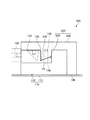
図1は、実施の形態1に係る光モジュール100の構成を模式的に示す側面図である。より具体的には、図1は、支持部材140の内側からみた光モジュール100の右側面図である。図1に示されるように、光モジュール100は、光電変換装置110および光レセプタクル120を有する。光レセプタクル120は、光レセプタクル本体130および支持部材140を有する。
[Embodiment 1]
(Configuration of optical module)
FIG. 1 is a side view schematically showing the configuration of the optical module 100 according to the first embodiment. More specifically, FIG. 1 is a right side view of the optical module 100 as viewed from the inside of the support member 140. As shown in FIG. 1, the optical module 100 includes a photoelectric conversion device 110 and an optical receptacle 120. The optical receptacle 120 includes an optical receptacle body 130 and a support member 140.

光モジュール100は、光伝送体150が接続された状態で使用される。光伝送体150の種類は、特に限定されず、必要に応じて適宜選択されうる。光伝送体150の種類の例には、光ファイバーおよび光導波路が含まれる。本実施の形態では、光伝送体150は、光ファイバーである。光ファイバーは、シングルモード方式であってもよいし、マルチモード方式であってもよい。光伝送体150の数は、特に限定されず、必要に応じて適宜選択されうる。本実施の形態では、12本の光ファイバーは、図1における紙面の奥行き方向に沿って、一定間隔で配列されている。なお、光伝送体150は、2列以上に配列されていてもよい。   The optical module 100 is used in a state where the optical transmission body 150 is connected. The type of the optical transmission body 150 is not particularly limited, and can be appropriately selected as necessary. Examples of types of optical transmission body 150 include optical fibers and optical waveguides. In the present embodiment, the optical transmission body 150 is an optical fiber. The optical fiber may be a single mode method or a multimode method. The number of the optical transmission bodies 150 is not particularly limited, and can be appropriately selected as necessary. In the present embodiment, the twelve optical fibers are arranged at regular intervals along the depth direction of the paper surface in FIG. Note that the optical transmitters 150 may be arranged in two or more rows.

光電変換装置110は、光モジュール100における光信号と電気信号とを互いに変換する。光電変換装置110は、基板111および光電変換素子112を有する。   The photoelectric conversion device 110 converts an optical signal and an electric signal in the optical module 100 to each other. The photoelectric conversion device 110 includes a substrate 111 and a photoelectric conversion element 112.

基板111は、光電変換素子112および支持部材140を支持している。基板111の例には、ガラスコンポジット基板、ガラスエポキシ基板およびフレキブシル基板が含まれる。   The substrate 111 supports the photoelectric conversion element 112 and the support member 140. Examples of the substrate 111 include a glass composite substrate, a glass epoxy substrate, and a flexible substrate.

光電変換素子112は、基板111上に配置されている。光電変換素子112は、発光素子または受光素子である。送信用の光モジュール100では、光電変換素子112として発光素子が使用される。受信用の光モジュール100では、光電変換素子112として受光素子が使用される。送受信用の光モジュール100では、光電変換素子112として発光素子および受光素子が使用される。本実施の形態に係る光モジュール100は、光伝送体150の端面への光の送信および光伝送体150の端面からの光の受信の両方を行うための送受信用光モジュールである。すなわち、光電変換装置110は、光電変換素子112として発光素子および受光素子を有する。   The photoelectric conversion element 112 is disposed on the substrate 111. The photoelectric conversion element 112 is a light emitting element or a light receiving element. In the transmission optical module 100, a light emitting element is used as the photoelectric conversion element 112. In the receiving optical module 100, a light receiving element is used as the photoelectric conversion element 112. In the optical module 100 for transmission / reception, a light emitting element and a light receiving element are used as the photoelectric conversion element 112. The optical module 100 according to the present embodiment is a transmission / reception optical module for performing both transmission of light to the end face of the optical transmission body 150 and reception of light from the end face of the optical transmission body 150. That is, the photoelectric conversion device 110 includes a light emitting element and a light receiving element as the photoelectric conversion element 112.

発光素子は、発光素子が配置された基板111の表面に対する垂直方向(法線方向)に光を出射する。発光素子の数は、特に限定されず、必要に応じて適宜設定されうる。たとえば、発光素子の数は、2個、4個、6個、8個または12個である。本実施の形態では、発光素子の数は、6個である。発光素子は、基板111上において、光レセプタクル本体130の第1光学面131(後述)に対向する位置に配置されている。6個の発光素子は、第1光学面131の配列方向および光伝送体150の配列方向(図1における紙面の奥行き方向)に沿って、一定間隔で配列されている。より具体的には、6個の発光素子は、同一直線上に位置するように配列されている。なお、光伝送体150が2列以上で配列されている場合は、発光素子も同じ列数で配列されうる。発光素子の例には、垂直共振器面発光レーザー(VCSEL)が含まれる。   The light emitting element emits light in a direction perpendicular to the surface of the substrate 111 on which the light emitting element is disposed (normal direction). The number of light emitting elements is not particularly limited, and can be set as appropriate. For example, the number of light emitting elements is 2, 4, 6, 8, or 12. In the present embodiment, the number of light emitting elements is six. The light emitting element is disposed on the substrate 111 at a position facing a first optical surface 131 (described later) of the optical receptacle body 130. The six light emitting elements are arranged at regular intervals along the arrangement direction of the first optical surface 131 and the arrangement direction of the optical transmission body 150 (the depth direction of the paper surface in FIG. 1). More specifically, the six light emitting elements are arranged so as to be positioned on the same straight line. In addition, when the optical transmission bodies 150 are arranged in two or more rows, the light emitting elements can also be arranged in the same number of rows. Examples of light emitting elements include vertical cavity surface emitting lasers (VCSEL).

受光素子は、光伝送体150の端面から出射された受信光を受光する。受光素子の数も、特に限定されず、必要に応じて適宜設定されうる。たとえば、受光素子の数は、2個、4個、6個、8個または12個である。本実施の形態では、受光素子の数は、6個である。受光素子も、光レセプタクル本体130の第1光学面131に対向する位置に配置されている。本実施の形態では、6個の受光素子は、第1光学面131の配列方向および光伝送体150の配列方向(図1における紙面の奥行き方向)に沿って、一定間隔で配列されている。より具体的には、6個の受光素子は、同一直線上に位置するように配列されている。なお、光伝送体150が2列以上に配列されている場合は、受光素子も同じ列数で配列されうる。受光素子は、例えば、フォトダイオードである。   The light receiving element receives the received light emitted from the end face of the optical transmission body 150. The number of light receiving elements is not particularly limited, and can be set as appropriate. For example, the number of light receiving elements is 2, 4, 6, 8, or 12. In the present embodiment, the number of light receiving elements is six. The light receiving element is also disposed at a position facing the first optical surface 131 of the optical receptacle body 130. In the present embodiment, the six light receiving elements are arranged at regular intervals along the arrangement direction of the first optical surface 131 and the arrangement direction of the optical transmitter 150 (the depth direction of the paper surface in FIG. 1). More specifically, the six light receiving elements are arranged so as to be positioned on the same straight line. When the optical transmission bodies 150 are arranged in two or more rows, the light receiving elements can be arranged in the same number of rows. The light receiving element is, for example, a photodiode.

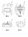
図2A〜Dは、光レセプタクル本体130の構成を示す図である。図2Aは、光レセプタクル本体130の平面図であり、図2Bは、底面図であり、図2Cは、正面図であり、図2Dは、右側面図である。なお、以下の説明では、光伝送体150の端面と対向する面を光レセプタクル本体130の正面として説明する(図1参照)。   2A to 2D are diagrams showing the configuration of the optical receptacle main body 130. 2A is a plan view of the optical receptacle main body 130, FIG. 2B is a bottom view, FIG. 2C is a front view, and FIG. 2D is a right side view. In the following description, the surface facing the end surface of the optical transmission body 150 will be described as the front surface of the optical receptacle body 130 (see FIG. 1).

光レセプタクル本体130は、光電変換装置110と光伝送体150との間に配置された状態で、光電変換素子112と、光伝送体150の端面とを光学的に結合する。本実施の形態では、光レセプタクル本体130は、6個の発光素子と、6本の光伝送体150の端面とをそれぞれ光学的に結合するとともに、6個の受光素子と、6本の光伝送体150の端面とをそれぞれ光学的に結合する。   The optical receptacle main body 130 optically couples the photoelectric conversion element 112 and the end face of the optical transmission body 150 while being disposed between the photoelectric conversion device 110 and the optical transmission body 150. In the present embodiment, the optical receptacle main body 130 optically couples the six light emitting elements and the end faces of the six optical transmission bodies 150, the six light receiving elements, and the six optical transmissions. The end surfaces of the body 150 are optically coupled to each other.

図2A〜Dに示されるように、光レセプタクル本体130は、略直方体形状の部材である。本実施の形態では、光レセプタクル本体130の天面には、光レセプタクル本体130の正面側から順に、第1凹部1301および第2凹部1302が形成されている。第1凹部1301の形状は、略五角柱形状であり、第2凹部1302の形状は、四角柱形状である。第1凹部1301および第2凹部1302は、光レセプタクル本体130の天面において、互いに離間して形成されている。すなわち、第1凹部1301および第2凹部1302の間には、壁部が形成される。   2A to 2D, the optical receptacle main body 130 is a substantially rectangular parallelepiped member. In the present embodiment, a first recess 1301 and a second recess 1302 are formed on the top surface of the optical receptacle body 130 in order from the front side of the optical receptacle body 130. The first recess 1301 has a substantially pentagonal prism shape, and the second recess 1302 has a quadrangular prism shape. The first recess 1301 and the second recess 1302 are formed on the top surface of the optical receptacle body 130 so as to be separated from each other. That is, a wall portion is formed between the first recess 1301 and the second recess 1302.

光レセプタクル本体130は、透光性を有する。光レセプタクル本体130は、発光素子から出射された送信光を光伝送体150の端面に向けて出射させるとともに、光伝送体150の端面から出射された受信光を受光素子に向けて出射させる。光レセプタクル本体130は、光通信に用いられる波長の光(送信光および受信光)に対して透光性を有する材料を用いて形成される。光レセプタクル本体130の材料の例には、ポリエーテルイミド(PEI)および環状オレフィン樹脂が含まれる。   The optical receptacle body 130 has translucency. The optical receptacle body 130 emits the transmission light emitted from the light emitting element toward the end face of the optical transmission body 150 and emits the reception light emitted from the end face of the optical transmission body 150 toward the light receiving element. The optical receptacle main body 130 is formed using a material having translucency with respect to light having a wavelength used for optical communication (transmitted light and received light). Examples of the material of the optical receptacle body 130 include polyetherimide (PEI) and cyclic olefin resin.

光レセプタクル本体130は、12個の第1光学面131と、12個の第2光学面132と、反射面133と、第1当接面134、第2当接面135、第3当接面136、2個の第1嵌合部137と、2個の接着用貫通孔138と、2個のフェルール用凸部139とを有する。第1当接面134、第2当接面135および第3当接面136は、光伝送体150の端面に対向する、光レセプタクル本体130の正面側から順に配置されている。光レセプタクル本体130の図2A〜Cの右側半分は、送信用の光レセプタクル本体130として機能し、光レセプタクル本体130の図2A〜Cの左側半分は、受信用の光レセプタクル本体130として機能する。   The optical receptacle main body 130 includes twelve first optical surfaces 131, twelve second optical surfaces 132, a reflecting surface 133, a first contact surface 134, a second contact surface 135, and a third contact surface. 136, two first fitting portions 137, two bonding through holes 138, and two ferrule convex portions 139. The first contact surface 134, the second contact surface 135, and the third contact surface 136 are sequentially arranged from the front side of the optical receptacle body 130 facing the end surface of the optical transmission body 150. 2A to 2C of the optical receptacle body 130 functions as an optical receptacle body 130 for transmission, and the left half of the optical receptacle body 130 in FIGS. 2A to 2C functions as an optical receptacle body 130 for reception.

図1に示されるように、光レセプタクル本体130は、第1当接面134、第2当接面135および第3当接面136で支持部材140に当接し、かつ支持部材140の設置面146を含む仮想平面(基板111の表面)と離間した状態で、接着用貫通孔138および接着用凹部148の内部に配置されている接着剤10を介して、支持部材140に接着されている。なお、本明細書中、「接着剤」には、硬化前の状態の接着剤と、硬化後の状態の接着剤(硬化物)との両方が含まれる。   As shown in FIG. 1, the optical receptacle main body 130 abuts the support member 140 at the first abutment surface 134, the second abutment surface 135, and the third abutment surface 136, and the installation surface 146 of the support member 140. In a state of being separated from a virtual plane including the surface (the surface of the substrate 111), it is bonded to the support member 140 via the adhesive 10 disposed inside the bonding through hole 138 and the bonding recess 148. In the present specification, “adhesive” includes both an adhesive in a state before curing and an adhesive (cured product) in a state after curing.

第1光学面131は、発光素子から出射された送信光を光レセプタクル本体130の内部に入射させる光学面である。また、第1光学面131は、光伝送体150の端面から出射され、光レセプタクル本体130の内部を通った受信光を受光素子に向けて出射させる光学面でもある。   The first optical surface 131 is an optical surface that causes the transmission light emitted from the light emitting element to enter the inside of the optical receptacle body 130. The first optical surface 131 is also an optical surface that emits the received light emitted from the end face of the optical transmission body 150 and passed through the inside of the optical receptacle body 130 toward the light receiving element.

本実施の形態では、第1光学面131の形状は、光電変換素子112に向かって凸形状の凸レンズ面である。第1光学面131は、発光素子から出射された送信光をコリメート光に変換させる。また、第1光学面131は、光レセプタクル本体130の内部を通った、光伝送体150からの受信光を収束させる。また、第1光学面131の平面視形状は、円形状である。   In the present embodiment, the shape of the first optical surface 131 is a convex lens surface that is convex toward the photoelectric conversion element 112. The first optical surface 131 converts transmission light emitted from the light emitting element into collimated light. The first optical surface 131 converges the received light from the optical transmission body 150 that has passed through the inside of the optical receptacle body 130. Further, the planar view shape of the first optical surface 131 is a circular shape.

本実施の形態では、第1光学面131の数は、12個である。第1光学面131は、光レセプタクル本体130の底面に形成されている凹部の底面に配置されている。12個の第1光学面131は、12個の光電変換素子112(6個の発光素子および6個の受光素子)とそれぞれ対向するように、光電変換素子112の配列方向に沿って配列されている。第1光学面131の中心軸(光軸)は、光電変換素子112の光電変換面に対して垂直であることが好ましい。また、第1光学面131の中心軸(光軸)は、発光素子から出射される送信光の光軸、および受光素子に入射する受信光の光軸と一致していることが好ましい。なお、光電変換素子112および光伝送体150が2列以上に配列されている場合は、第1光学面131も同じ列数で配列される。   In the present embodiment, the number of first optical surfaces 131 is twelve. The first optical surface 131 is disposed on the bottom surface of the recess formed on the bottom surface of the optical receptacle body 130. The twelve first optical surfaces 131 are arranged along the arrangement direction of the photoelectric conversion elements 112 so as to face the twelve photoelectric conversion elements 112 (six light emitting elements and six light receiving elements). Yes. The central axis (optical axis) of the first optical surface 131 is preferably perpendicular to the photoelectric conversion surface of the photoelectric conversion element 112. The central axis (optical axis) of the first optical surface 131 preferably coincides with the optical axis of transmission light emitted from the light emitting element and the optical axis of reception light incident on the light receiving element. In addition, when the photoelectric conversion elements 112 and the optical transmission bodies 150 are arranged in two or more rows, the first optical surfaces 131 are also arranged in the same number of rows.

本実施の形態では、12個の第1光学面131のうち、図2Bの右側の6個の第1光学面131は、送信用の第1光学面131として使用され、左側の6個の第1光学面131は、受信用の第1光学面131として使用される。発光素子からの送信光は、送信用の第1光学面131で光レセプタクル本体130の内部に入射し、光レセプタクル本体130の内部を通った受信光は、受信用の第1光学面131から出射する。   In the present embodiment, among the twelve first optical surfaces 131, the six first optical surfaces 131 on the right side in FIG. 2B are used as the first optical surfaces 131 for transmission, and the six first optical surfaces 131 on the left side. The first optical surface 131 is used as the first optical surface 131 for reception. Transmitted light from the light emitting element is incident on the inside of the optical receptacle body 130 at the first optical surface 131 for transmission, and received light that has passed through the interior of the optical receptacle body 130 is emitted from the first optical surface 131 for reception. To do.

第2光学面132は、発光素子から出射され、光レセプタクル本体130の内部を通った送信光を光伝送体150の端面に向けて出射させる光学面である。また、第2光学面132は、光伝送体150の端面から出射された受信光を光レセプタクル本体130の内部に入射させる光学面でもある。   The second optical surface 132 is an optical surface that emits transmission light emitted from the light emitting element and passed through the inside of the optical receptacle main body 130 toward the end surface of the optical transmission body 150. The second optical surface 132 is also an optical surface that causes the received light emitted from the end surface of the optical transmission body 150 to enter the inside of the optical receptacle main body 130.

本実施の形態では、第2光学面132の形状は、光伝送体150の端面に向かって凸状の凸レンズ面である。第2光学面132は、光レセプタクル本体130の内部を通った送信光を光伝送体150の端面に向けて収束させる。また、光伝送体150の端面から出射された受信光をコリメート光に変換させる。また、第2光学面132の平面視形状は、円形状である。   In the present embodiment, the shape of the second optical surface 132 is a convex lens surface that is convex toward the end surface of the optical transmission body 150. The second optical surface 132 converges the transmission light that has passed through the inside of the optical receptacle body 130 toward the end surface of the optical transmission body 150. Further, the received light emitted from the end face of the optical transmission body 150 is converted into collimated light. Further, the planar view shape of the second optical surface 132 is a circular shape.

本実施の形態では、第2光学面132の数は、12個である。第2光学面132は、光レセプタクル本体130の正面に形成されている凹部の底面に配置されている。12個の第2光学面132は、12本の光伝送体150の端面とそれぞれ対向するように、光伝送体150の配列方向に沿って配列されている。第2光学面132の中心軸(光軸)は、光伝送体150の端面に対して垂直であることが好ましい。また、第2光学面132の中心軸(光軸)は、光伝送体150から出射される受信光の光軸、および光伝送体150に入射する送信光の光軸と一致していることが好ましい。なお、光電変換素子112および光伝送体150が2列以上に配列されている場合は、第2光学面132も同じ列数で配列される。   In the present embodiment, the number of second optical surfaces 132 is twelve. The second optical surface 132 is disposed on the bottom surface of a recess formed on the front surface of the optical receptacle body 130. The twelve second optical surfaces 132 are arranged along the arrangement direction of the optical transmitters 150 so as to face the end surfaces of the twelve optical transmitters 150, respectively. The central axis (optical axis) of the second optical surface 132 is preferably perpendicular to the end surface of the optical transmission body 150. In addition, the central axis (optical axis) of the second optical surface 132 coincides with the optical axis of the reception light emitted from the optical transmission body 150 and the optical axis of the transmission light incident on the optical transmission body 150. preferable. When the photoelectric conversion elements 112 and the optical transmission bodies 150 are arranged in two or more rows, the second optical surfaces 132 are also arranged in the same number of rows.

本実施の形態では、12個の第2光学面132のうち、図2Cの右側の6個の第2光学面132は、送信用の第2光学面132として使用され、左側の6個の第2光学面132は、受信用の第2光学面132として使用される。光レセプタクル本体130の内部を通った送信光は、送信用の第2光学面132から出射し、光伝送体150からの受信光は、受信用の第2光学面132で光レセプタクル本体130の内部に入射する。   In the present embodiment, among the 12 second optical surfaces 132, the six second optical surfaces 132 on the right side in FIG. 2C are used as the second optical surfaces 132 for transmission, and the six second optical surfaces 132 on the left side are used. The second optical surface 132 is used as the second optical surface 132 for reception. The transmitted light that has passed through the inside of the optical receptacle body 130 is emitted from the second optical surface 132 for transmission, and the received light from the optical transmission body 150 is transmitted to the interior of the optical receptacle body 130 at the second optical surface 132 for reception. Is incident on.

反射面133は、第1光学面131で光レセプタクル本体130の内部に入射した送信光を第2光学面132に向けて反射させる。また、反射面133は、第2光学面132で光レセプタクル本体130の内部に入射した受信光を第1光学面131に向けて反射させる。反射面133は、光レセプタクル本体130の天面に形成されている第1凹部1301の内面の一部である。反射面133は、第2光学面132が配置された面(光レセプタクル本体130の正面)と、第2当接面135との間に配置されている。   The reflection surface 133 reflects the transmission light incident on the inside of the optical receptacle body 130 by the first optical surface 131 toward the second optical surface 132. The reflection surface 133 reflects the reception light incident on the inside of the optical receptacle main body 130 by the second optical surface 132 toward the first optical surface 131. The reflective surface 133 is a part of the inner surface of the first recess 1301 formed on the top surface of the optical receptacle body 130. The reflecting surface 133 is disposed between the surface on which the second optical surface 132 is disposed (the front surface of the optical receptacle main body 130) and the second contact surface 135.

本実施の形態では、反射面133は、光レセプタクル本体130の天面から底面に向かうにつれて第2光学面132(光伝送体150)から離れるように傾斜している。反射面133の傾斜角は、第1光学面131の光軸および第2光学面132の光軸に対して45°である。   In the present embodiment, the reflecting surface 133 is inclined so as to move away from the second optical surface 132 (the optical transmission body 150) as it goes from the top surface to the bottom surface of the optical receptacle body 130. The inclination angle of the reflecting surface 133 is 45 ° with respect to the optical axis of the first optical surface 131 and the optical axis of the second optical surface 132.

第1当接面134は、光レセプタクル本体130の天面の一部である。第1当接面134は、支持部材140の内面と当接している。第1当接面134は、第1光学面131が配置された面(光レセプタクル本体130の底面)の反対側に配置されている。   The first contact surface 134 is a part of the top surface of the optical receptacle body 130. The first contact surface 134 is in contact with the inner surface of the support member 140. The first contact surface 134 is disposed on the opposite side of the surface on which the first optical surface 131 is disposed (the bottom surface of the optical receptacle body 130).

第2当接面135は、第2凹部1302の側面である。第2当接面135も、支持部材140の内面と当接している。本実施の形態では、第2当接面135は、支持部材140の内面に形成されている凸部1411(図3A参照)の側面と当接している。第2当接面135は、第2光学面132が配置された面(光レセプタクル本体130の正面)の反対側に配置されている。第2当接面135は、光伝送体150の端面と第2光学面132との対向方向に対して直交する方向に沿うように配置されている。本実施の形態では、第2当接面135は、第2光学面132が配置された面と平行であり、第2光学面132の光軸(中心軸)に対して垂直である。   The second contact surface 135 is a side surface of the second recess 1302. The second contact surface 135 is also in contact with the inner surface of the support member 140. In the present embodiment, the second contact surface 135 is in contact with the side surface of the convex portion 1411 (see FIG. 3A) formed on the inner surface of the support member 140. The second contact surface 135 is disposed on the opposite side of the surface on which the second optical surface 132 is disposed (the front surface of the optical receptacle main body 130). The second contact surface 135 is disposed along a direction orthogonal to the facing direction of the end surface of the optical transmission body 150 and the second optical surface 132. In the present embodiment, the second contact surface 135 is parallel to the surface on which the second optical surface 132 is disposed and is perpendicular to the optical axis (center axis) of the second optical surface 132.

第3当接面136は、第2凹部1302の底面である。第3当接面136は、第1光学面131が配置された面(光レセプタクル本体130の底面)の反対側に配置されている。第3当接面136と、光レセプタクル本体130の底面との間隔は、第1当接面134と、光レセプタクル本体130の底面との間隔より小さい。第3当接面136も、支持部材140の内面と当接している。第3当接面136は、支持部材140の内面に形成されている凸部1411の頂面と当接している。第3当接面136は、第1当接面134と平行であってもよいし、平行でなくてもよい。本実施の形態では、第3当接面136は、第1当接面134と平行である。   The third contact surface 136 is the bottom surface of the second recess 1302. The third contact surface 136 is disposed on the opposite side of the surface on which the first optical surface 131 is disposed (the bottom surface of the optical receptacle body 130). The distance between the third contact surface 136 and the bottom surface of the optical receptacle body 130 is smaller than the distance between the first contact surface 134 and the bottom surface of the optical receptacle body 130. The third contact surface 136 is also in contact with the inner surface of the support member 140. The third contact surface 136 is in contact with the top surface of the convex portion 1411 formed on the inner surface of the support member 140. The third contact surface 136 may or may not be parallel to the first contact surface 134. In the present embodiment, the third contact surface 136 is parallel to the first contact surface 134.

第1嵌合部137は、光レセプタクル本体130の第1当接面134に配置されており、支持部材140の第2嵌合部147(図3A参照)に嵌合されている。第1嵌合部137および第2嵌合部147が、互いに嵌合されていることによって、支持部材140に支持される光レセプタクル本体130の位置が決定されうる。   The first fitting portion 137 is disposed on the first contact surface 134 of the optical receptacle body 130 and is fitted to the second fitting portion 147 (see FIG. 3A) of the support member 140. By fitting the first fitting portion 137 and the second fitting portion 147 with each other, the position of the optical receptacle body 130 supported by the support member 140 can be determined.

第1嵌合部137の位置、形状、大きさ、および数は、上記機能を発揮することができれば特に限定されず、支持部材140の第2嵌合部147の位置、形状、大きさ、および数にそれぞれ対応する。本実施の形態では、第1嵌合部137の数は、2個である。2個の第1嵌合部137は、光レセプタクル本体130の右側面および左側面の対向方向に沿って、第1凹部1301の両側に配置されている。第1嵌合部137の形状の例には、円柱形状、多角柱形状および貫通孔形状が含まれる。本実施の形態では、第1嵌合部137は、円柱形状の凹部である。   The position, shape, size, and number of the first fitting portion 137 are not particularly limited as long as the above functions can be exhibited, and the position, shape, size, and size of the second fitting portion 147 of the support member 140 are not limited. Each corresponds to a number. In the present embodiment, the number of first fitting portions 137 is two. The two first fitting portions 137 are arranged on both sides of the first recess 1301 along the opposing direction of the right side surface and the left side surface of the optical receptacle body 130. Examples of the shape of the first fitting portion 137 include a columnar shape, a polygonal column shape, and a through-hole shape. In the present embodiment, the first fitting portion 137 is a cylindrical recess.

接着用貫通孔138は、第3当接面136と、第3当接面136の反対側に位置している面(光レセプタクル本体130の底面)とに開口している。接着用貫通孔138の内部には、接着剤10が配置されている。光レセプタクル本体130および支持部材140は、接着剤10を介して互いに接着されている。   The bonding through-hole 138 opens to the third contact surface 136 and a surface (the bottom surface of the optical receptacle main body 130) located on the opposite side of the third contact surface 136. An adhesive 10 is disposed inside the bonding through hole 138. The optical receptacle body 130 and the support member 140 are bonded to each other via the adhesive 10.

接着用貫通孔138の位置、形状、大きさおよび数は、接着用貫通孔138の内部に接着剤10が配置されることができれば、特に限定されない。接着用貫通孔138の位置および数は、後述の接着用凹部148の位置および数にそれぞれ対応している。本実施の形態では、接着用貫通孔138の数は、2個である。2個の接着用貫通孔138は、光レセプタクル本体130の右側面および左側面の対向方向に沿って、第3当接面136の両端部に配置されている。接着用貫通孔138の形状の例には、円柱形状および多角柱形状が含まれる。本実施の形態では、接着用貫通孔138の形状は、円柱形状である。接着用貫通孔138の大きさは、第3当接面136の反対側に位置している面から第3当接面136に亘って、同じであってもよいし、同じでなくてもよい(後述の変形例3参照)。本実施の形態では、接着用貫通孔138の大きさは、第3当接面136の反対側に位置している面から第3当接面136に亘って、同じである。   The position, shape, size, and number of the bonding through holes 138 are not particularly limited as long as the adhesive 10 can be disposed inside the bonding through holes 138. The positions and the number of bonding through holes 138 correspond to the positions and the number of bonding concaves 148 described later, respectively. In the present embodiment, the number of bonding through holes 138 is two. The two bonding through holes 138 are disposed at both ends of the third contact surface 136 along the opposing direction of the right side surface and the left side surface of the optical receptacle main body 130. Examples of the shape of the bonding through hole 138 include a cylindrical shape and a polygonal column shape. In the present embodiment, the shape of the bonding through-hole 138 is a cylindrical shape. The size of the bonding through-hole 138 may or may not be the same from the surface located on the opposite side of the third contact surface 136 to the third contact surface 136. (Refer to Modification 3 described later). In the present embodiment, the size of the bonding through hole 138 is the same from the surface located on the opposite side of the third contact surface 136 to the third contact surface 136.

フェルール用凸部139は、例えば、光伝送体150を保持するためのフェルールに形成されている嵌合部に嵌合される。これにより、光レセプタクル本体130の正面の面内方向において、光レセプタクル本体130に対する光伝送体150の相対位置が決定されうる。フェルール用凸部139の位置、形状、大きさおよび数は、上記機能を発揮することができれば特に限定されず、フェルールの嵌合部の位置、形状、大きさおよび数にそれぞれ対応する。本実施の形態では、フェルール用凸部139の数は、2個である。2個のフェルール用凸部139は、光レセプタクル本体130の正面に配置されている。本実施の形態では、フェルール用凸部139は、第2光学面132の配列方向に沿って、第2光学面132の両側に配置されている。フェルール用凸部139の形状は、先端部が半球形状である円柱形状である。   The ferrule convex portion 139 is fitted into a fitting portion formed on the ferrule for holding the optical transmission body 150, for example. Accordingly, the relative position of the optical transmission body 150 with respect to the optical receptacle body 130 can be determined in the in-plane direction of the front surface of the optical receptacle body 130. The position, shape, size, and number of the ferrule convex portions 139 are not particularly limited as long as the above functions can be exhibited, and correspond to the position, shape, size, and number of the fitting portions of the ferrule. In the present embodiment, the number of ferrule convex portions 139 is two. The two ferrule projections 139 are arranged on the front surface of the optical receptacle main body 130. In the present embodiment, the ferrule convex portions 139 are arranged on both sides of the second optical surface 132 along the arrangement direction of the second optical surfaces 132. The ferrule convex portion 139 has a cylindrical shape with a hemispherical tip.

図3A〜Dは、支持部材140の構成を示す図である。図3Aは、支持部材140の底面図であり、図3Bは、正面図であり、図3Cは、右側面図であり、図3Dは、図3AのD−D線における断面図である。なお、以下の説明では、光レセプタクル本体130の正面と同じ方向に向いて配置されている面を支持部材140の正面として説明する。   3A to 3D are diagrams illustrating the configuration of the support member 140. 3A is a bottom view of the support member 140, FIG. 3B is a front view, FIG. 3C is a right side view, and FIG. 3D is a cross-sectional view taken along the line DD of FIG. 3A. In the following description, the surface disposed in the same direction as the front surface of the optical receptacle body 130 will be described as the front surface of the support member 140.

図1に示されるように、支持部材140は、基板111および光レセプタクル本体130が互いに離間した状態で、光レセプタクル本体130を支持している。支持部材140は、光レセプタクル本体130の第1当接面134、第2当接面135および第3当接面136に当接している。支持部材140の形状および大きさは、光電変換素子112および光伝送体150の間の光路を通る光の進行の妨げにならず、かつ光レセプタクル本体130の第1当接面134、第2当接面135および第3当接面136に当接した状態で、光レセプタクル本体130を支持することができれば特に限定されない。本実施の形態では、支持部材140は、底面(基板111に対向する面)に形成された凹部内において、光レセプタクル本体130を支持している。支持部材140に形成された凹部の底面(内部空間の天面)の形状は、光レセプタクル本体130の天面の形状に対応している。   As shown in FIG. 1, the support member 140 supports the optical receptacle body 130 in a state where the substrate 111 and the optical receptacle body 130 are separated from each other. The support member 140 is in contact with the first contact surface 134, the second contact surface 135, and the third contact surface 136 of the optical receptacle body 130. The shape and size of the support member 140 do not hinder the progress of light passing through the optical path between the photoelectric conversion element 112 and the optical transmission body 150, and the first contact surface 134 and the second contact surface of the optical receptacle body 130. There is no particular limitation as long as the optical receptacle main body 130 can be supported while being in contact with the contact surface 135 and the third contact surface 136. In the present embodiment, the support member 140 supports the optical receptacle body 130 in a recess formed on the bottom surface (the surface facing the substrate 111). The shape of the bottom surface (the top surface of the internal space) of the recess formed in the support member 140 corresponds to the shape of the top surface of the optical receptacle body 130.

本実施の形態では、支持部材140は、天板141、右側板142、左側板143、前板144および背板145により構成されている。支持部材140を構成する各部材は、一体として形成されていてもよいし、別体として形成されていてもよい。本実施の形態では、支持部材140を構成する各部材は、一体として形成されている。   In the present embodiment, the support member 140 includes a top plate 141, a right side plate 142, a left side plate 143, a front plate 144, and a back plate 145. Each member constituting the support member 140 may be formed integrally or may be formed separately. In the present embodiment, the members constituting the support member 140 are integrally formed.

天板141は、右側板142、左側板143、前板144および背板145により形成される2つの開口のうち、一方の開口を覆う領域に配置されている。天板141の一方の面(支持部材140の内面)は、光レセプタクル本体130の天面の一部に当接している。天板141の一方の面の形状は、光レセプタクル本体130の天面に当接することができれば特に限定されず、光レセプタクル本体130の天面の形状に対応している。本実施の形態では、天板141の当該一方の面には、凸部1411が形成されている。凸部1411における、光レセプタクル本体130の正面側に配置された面は、光レセプタクル本体130の第2凹部1302の側面(第2当接面135)に当接している。凸部1411における、光レセプタクル本体130の底面側の面は、光レセプタクル本体130の第2凹部1302の底面(第3当接面136)に当接している。これにより、光レセプタクル本体130の天面と、支持部材140の内面とが互いに当接した状態で、支持部材140は、光レセプタクル本体130を支持することができる。   The top plate 141 is disposed in a region covering one of the two openings formed by the right side plate 142, the left side plate 143, the front plate 144, and the back plate 145. One surface of the top plate 141 (the inner surface of the support member 140) is in contact with a part of the top surface of the optical receptacle body 130. The shape of one surface of the top plate 141 is not particularly limited as long as it can contact the top surface of the optical receptacle main body 130, and corresponds to the shape of the top surface of the optical receptacle main body 130. In the present embodiment, a convex portion 1411 is formed on the one surface of the top plate 141. The surface of the convex portion 1411 disposed on the front side of the optical receptacle body 130 is in contact with the side surface (second contact surface 135) of the second recess 1302 of the optical receptacle body 130. The surface of the convex portion 1411 on the bottom surface side of the optical receptacle body 130 is in contact with the bottom surface (third contact surface 136) of the second recess 1302 of the optical receptacle body 130. Accordingly, the support member 140 can support the optical receptacle body 130 in a state where the top surface of the optical receptacle body 130 and the inner surface of the support member 140 are in contact with each other.

右側板142の一方の面(支持部材140の内面)は、光レセプタクル本体130の右側面と対向している。右側板142の当該一方の面と、光レセプタクル本体130の右側面とは、互いに接していてもよいし、互いに離間していてもよい。本実施の形態では、一対の右側板142の当該一方の面と、光レセプタクル本体130の右側面とは、互いに離間している。   One surface of the right side plate 142 (the inner surface of the support member 140) faces the right side surface of the optical receptacle body 130. The one side surface of the right side plate 142 and the right side surface of the optical receptacle main body 130 may be in contact with each other or may be separated from each other. In the present embodiment, the one surface of the pair of right side plates 142 and the right side surface of the optical receptacle body 130 are separated from each other.

左側板143の一方の面(支持部材140の内面)は、光レセプタクル本体130の左側面と対向している。左側板143の当該一方の面と、光レセプタクル本体130の左側面とは、互いに接していてもよいし、互いに離間していてもよい。本実施の形態では、一対の左側板143の当該一方の面と、光レセプタクル本体130の左側面とは、互いに離間している。   One surface of the left side plate 143 (the inner surface of the support member 140) faces the left side surface of the optical receptacle body 130. The one surface of the left side plate 143 and the left side surface of the optical receptacle body 130 may be in contact with each other or may be separated from each other. In the present embodiment, the one surface of the pair of left side plates 143 and the left side surface of the optical receptacle body 130 are separated from each other.

前板144には、開口部1441が形成されている。これにより、光伝送体150は、前板144側から光レセプタクル本体130に接続されうる。   An opening 1441 is formed in the front plate 144. Thereby, the optical transmission body 150 can be connected to the optical receptacle main body 130 from the front plate 144 side.

背板145の一方の面(支持部材140の内面)は、光レセプタクル本体130の背面の一部と対向している。背板145の当該一方の面と、光レセプタクル本体130の背面とは、互いに接していてもよいし、互いに離間していてもよい。本実施の形態では、背板145の当該一方の面と、光レセプタクル本体130の背面とは、互いに離間している。   One surface of the back plate 145 (the inner surface of the support member 140) faces a part of the back surface of the optical receptacle body 130. The one surface of the back plate 145 and the back surface of the optical receptacle body 130 may be in contact with each other or may be separated from each other. In the present embodiment, the one surface of the back plate 145 and the back surface of the optical receptacle body 130 are separated from each other.

支持部材140は、設置面146、第2嵌合部147および接着用凹部148を有する。   The support member 140 has an installation surface 146, a second fitting portion 147, and an adhesive recess 148.

設置面146は、支持部材140における基板111に設置されるための面である。本実施の形態では、設置面146は、右側板142、左側板143、前板144および背板145の下面(底面)である。右側板142、左側板143、前板144および背板145の高さ方向の長さは、互いに同じである。右側板142、左側板143、前板144および背板145の高さ方向の長さは、光レセプタクル本体130の高さより長い。これにより、支持部材140が基板111上に配置されたとき、光レセプタクル本体130は、基板111の表面(設置面146を含む仮想平面)から離間した状態で支持部材140に支持されうる。また、換言すると、光モジュール100において、光レセプタクル本体130および基板111の間には、空間が形成されている。   The installation surface 146 is a surface for installation on the substrate 111 in the support member 140. In the present embodiment, the installation surface 146 is the lower surface (bottom surface) of the right side plate 142, the left side plate 143, the front plate 144, and the back plate 145. The lengths of the right side plate 142, the left side plate 143, the front plate 144, and the back plate 145 in the height direction are the same. The lengths of the right side plate 142, the left side plate 143, the front plate 144, and the back plate 145 in the height direction are longer than the height of the optical receptacle body 130. As a result, when the support member 140 is disposed on the substrate 111, the optical receptacle body 130 can be supported by the support member 140 in a state of being separated from the surface of the substrate 111 (a virtual plane including the installation surface 146). In other words, in the optical module 100, a space is formed between the optical receptacle body 130 and the substrate 111.

第2嵌合部147は、第1当接面134に対向する面に配置されている。第2嵌合部147は、光レセプタクル本体130の第1嵌合部137に嵌合されている。第1嵌合部137および第2嵌合部147が、互いに嵌合されていることによって、支持部材140に支持される光レセプタクル本体130の位置が決定されうる。   The second fitting portion 147 is disposed on the surface facing the first contact surface 134. The second fitting portion 147 is fitted to the first fitting portion 137 of the optical receptacle body 130. By fitting the first fitting portion 137 and the second fitting portion 147 with each other, the position of the optical receptacle body 130 supported by the support member 140 can be determined.

第2嵌合部147の位置、形状、大きさ、および数は、上記機能を発揮することができれば特に限定されず、光レセプタクル本体130の第1嵌合部137の位置、形状、大きさおよび数にそれぞれ対応する。本実施の形態では、第2嵌合部147の数は、2個である。2個の第2嵌合部147は、右側板142および左側板143の対向方向に沿って配置されている。第2嵌合部147の形状の例には、円柱形状、多角柱形状および貫通孔形状が含まれる。本実施の形態では、第2嵌合部147は、円柱形状の凸部である。   The position, shape, size, and number of the second fitting portions 147 are not particularly limited as long as the above functions can be exhibited. The position, shape, size, and number of the first fitting portions 137 of the optical receptacle body 130 are not limited. Each corresponds to a number. In the present embodiment, the number of second fitting portions 147 is two. The two second fitting portions 147 are arranged along the facing direction of the right side plate 142 and the left side plate 143. Examples of the shape of the second fitting portion 147 include a cylindrical shape, a polygonal column shape, and a through-hole shape. In the present embodiment, the second fitting portion 147 is a cylindrical convex portion.

接着用凹部148は、第3当接面136に対向する面に開口し、かつ接着用貫通孔138に連通している。本実施の形態では、接着用凹部148は、天板141に形成されている凸部1411の天面に開口している。接着用凹部148の内部には、接着剤10が配置されている。前述のとおり、光レセプタクル本体130および支持部材140は、接着剤10を介して互いに接着されている。   The bonding recess 148 opens to a surface facing the third contact surface 136 and communicates with the bonding through hole 138. In the present embodiment, the bonding concave portion 148 is opened on the top surface of the convex portion 1411 formed on the top plate 141. The adhesive 10 is disposed inside the bonding recess 148. As described above, the optical receptacle main body 130 and the support member 140 are bonded to each other via the adhesive 10.

接着用凹部148の位置、形状、大きさおよび数は、接着用貫通孔138を介して接着用凹部148の内部に接着剤を充填し硬化させることができれば、特に限定されない。接着用凹部148の位置および数は、接着用貫通孔138の位置および数にそれぞれ対応している。本実施の形態では、接着用貫通孔138の数は、2個であり、2個の右側板142および左側板143の対向方向に沿って配置されている。接着用凹部148の形状の例には、円柱形状および多角柱形状が含まれる。本実施の形態では、接着用凹部148の形状は、円柱形状である。接着用凹部148の大きさは、接着用凹部148の底面から、接着用凹部148の開口部に亘って、同じであってもよいし、同じでなくてもよい。本実施の形態では、接着用凹部148の大きさは、接着用凹部148の底面から、接着用凹部148の開口部に亘って同じである。   The position, shape, size and number of the bonding recesses 148 are not particularly limited as long as the adhesive can be filled and cured inside the bonding recesses 148 through the bonding through holes 138. The position and number of the bonding recesses 148 correspond to the position and number of the bonding through holes 138, respectively. In the present embodiment, the number of bonding through holes 138 is two, and the bonding through holes 138 are arranged along the opposing direction of the two right side plates 142 and 143. Examples of the shape of the bonding recess 148 include a cylindrical shape and a polygonal column shape. In the present embodiment, the shape of the bonding recess 148 is a cylindrical shape. The size of the bonding recess 148 may or may not be the same from the bottom surface of the bonding recess 148 to the opening of the bonding recess 148. In the present embodiment, the size of the bonding recess 148 is the same from the bottom surface of the bonding recess 148 to the opening of the bonding recess 148.

また、接着用貫通孔138の第3当接面136側の開口部の大きさと、接着用凹部148の開口部の大きさとは、互いに同じであってもよいし、互いに異なっていてもよい(後述の変形例1、2参照)。本実施の形態では、接着用貫通孔138の第3当接面136側の開口部の大きさと、接着用凹部148の開口部の大きさとは、互いに同じである。本明細書中、「開口部の大きさ」とは、貫通孔または凹部の開口面内の、開口面の中心(重心)を通る任意の方向における、貫通孔または凹部の開口長さをいう。たとえば、貫通孔または凹部の開口端面の形状が、円形状である場合には、貫通孔または凹部の開口部の大きさは、当該開口端面の直径である。   In addition, the size of the opening on the third contact surface 136 side of the bonding through-hole 138 and the size of the opening of the bonding recess 148 may be the same or different from each other ( (See Modifications 1 and 2 below). In the present embodiment, the size of the opening on the third contact surface 136 side of the bonding through hole 138 and the size of the opening of the bonding recess 148 are the same. In the present specification, the “size of the opening” means the opening length of the through hole or the recess in any direction passing through the center (center of gravity) of the opening surface in the opening surface of the through hole or the recess. For example, when the shape of the opening end surface of the through hole or the recess is circular, the size of the opening of the through hole or the recess is the diameter of the opening end surface.

支持部材140は、透光性を有する材料で形成されていてもよいし、透光性を有しない材料で形成されていてもよい。支持部材140の材料の例には、ポリカーボネート(PC)、ポリエーテルイミド(PEI)およびポリエーテルサルフォン(PES)が含まれる。   The support member 140 may be formed of a light-transmitting material or may be formed of a material that does not have light-transmitting properties. Examples of the material of the support member 140 include polycarbonate (PC), polyetherimide (PEI), and polyethersulfone (PES).

(光モジュールの製造方法)
光モジュール100の製造方法は、特に限定されない。たとえば、光モジュール100は、以下に説明する製造方法により製造されうる。
(Optical module manufacturing method)
The manufacturing method of the optical module 100 is not particularly limited. For example, the optical module 100 can be manufactured by a manufacturing method described below.

光モジュール100の製造方法は、光レセプタクル本体130および支持部材140を互いに固定する第1工程と、光レセプタクル本体130が固定された支持部材140と、基板111とを互いに固定する第2工程と、を含む。   The method for manufacturing the optical module 100 includes a first step of fixing the optical receptacle body 130 and the support member 140 to each other, a second step of fixing the support member 140 to which the optical receptacle body 130 is fixed, and the substrate 111 to each other, including.

1)第1工程
第1工程では、光レセプタクル本体130および支持部材140を互いに固定する。まず、光レセプタクル本体130および支持部材140を準備する。光レセプタクル本体130および支持部材140は、例えば、射出成形により製造されうる。
1) First Step In the first step, the optical receptacle body 130 and the support member 140 are fixed to each other. First, the optical receptacle main body 130 and the support member 140 are prepared. The optical receptacle main body 130 and the support member 140 can be manufactured by injection molding, for example.

次いで、準備した光レセプタクル本体130を準備した支持部材140の所定の位置に配置し、固定する。より具体的には、第1当接面134、第2当接面135および第3当接面136で、光レセプタクル本体130を支持部材140に当接させるとともに、光レセプタクル本体130の第1嵌合部137を、支持部材140の第2嵌合部147に嵌合させる。これにより、光レセプタクル本体130が位置決めされ、光レセプタクル本体130の接着用貫通孔138と、支持部材140の接着用凹部148とが互いに連通した状態で、光レセプタクル本体130および支持部材140が、互いに連結される。本実施の形態では、光レセプタクル本体130の天面と、支持部材140の天面とを下に向けた状態で、光レセプタクル本体130を、支持部材140の底面側から所定の位置に配置する。   Next, the prepared optical receptacle main body 130 is arranged at a predetermined position of the prepared support member 140 and fixed. More specifically, the optical receptacle body 130 is brought into contact with the support member 140 at the first contact surface 134, the second contact surface 135, and the third contact surface 136, and the first fitting of the optical receptacle body 130 is performed. The joint portion 137 is fitted to the second fitting portion 147 of the support member 140. As a result, the optical receptacle body 130 is positioned, and the optical receptacle body 130 and the support member 140 are connected to each other in a state where the bonding through-hole 138 of the optical receptacle body 130 and the bonding recess 148 of the support member 140 are in communication with each other. Connected. In the present embodiment, the optical receptacle body 130 is disposed at a predetermined position from the bottom surface side of the support member 140 with the top surface of the optical receptacle body 130 and the top surface of the support member 140 facing downward.

第1当接面134、第2当接面135および第3当接面136で、光レセプタクル本体130を支持部材140に当接させた状態で、接着用貫通孔138および接着用凹部148の内部に接着剤を注入し、硬化させる。これにより、光レセプタクル本体130および支持部材140は、接着用貫通孔138および接着用凹部148の内部に配置された接着剤10を介して、互いに接着されうる。本実施の形態では、光レセプタクル本体130の天面と、支持部材140の天面とを下に向けた状態で、光レセプタクル本体130の底面側から接着用貫通孔138および接着用凹部148の内部に接着剤を注入する。   In the state where the optical receptacle body 130 is in contact with the support member 140 with the first contact surface 134, the second contact surface 135, and the third contact surface 136, the inside of the bonding through hole 138 and the bonding recess 148 Adhesive is poured into and cured. Thereby, the optical receptacle main body 130 and the support member 140 can be bonded to each other via the adhesive 10 disposed inside the bonding through hole 138 and the bonding recess 148. In the present embodiment, with the top surface of the optical receptacle body 130 and the top surface of the support member 140 facing downward, the inside of the bonding through-hole 138 and the bonding recess 148 from the bottom surface side of the optical receptacle body 130. Inject adhesive.

前述のとおり、反射面133は、第2光学面132が配置された面(光レセプタクル本体130の正面)と、第2当接面135との間に配置されており、第1凹部1301および第2凹部1302の間には、壁部が配置されている。このため、接着用貫通孔138側から接着剤を注入するときに、接着剤は、光レセプタクル本体130の第3当接面136と、支持部材140の第3当接面136に対向する面との間に流れ込んだとしても、反射面133に到達することがない。このように、本実施の形態では、接着剤が、光学面(反射面133)に付着することによる、光レセプタクル120の光学特性の低下を抑制することができる。   As described above, the reflection surface 133 is disposed between the surface on which the second optical surface 132 is disposed (the front surface of the optical receptacle body 130) and the second contact surface 135, and the first recess 1301 and the first Between the two recesses 1302, a wall portion is disposed. For this reason, when injecting the adhesive from the bonding through hole 138 side, the adhesive includes a third contact surface 136 of the optical receptacle body 130 and a surface facing the third contact surface 136 of the support member 140. Even if it flows in between, the reflective surface 133 is not reached. Thus, in this Embodiment, the adhesive agent adheres to an optical surface (reflecting surface 133), and the fall of the optical characteristic of the optical receptacle 120 can be suppressed.

2)第2工程
第2工程では、基板111および光レセプタクル本体130が互いに離間した状態で、光レセプタクル本体130が固定された支持部材140(光レセプタクル120)と、基板111とを互いに固定する。まず、基板111に光電変換素子112(発光素子および受光素子)が実装された光電変換装置110を準備する。たとえば、光電変換装置110は、市販品として購入されうる。次いで、光レセプタクル120を光電変換装置110上に配置し、固定する。より具体的には、光レセプタクル本体130の第1光学面131および光電変換素子112の光電変換面が互いに対向するように位置合わせし、光レセプタクル120の支持部材140および光電変換装置110の基板111を互いに固定する。これにより、光レセプタクル120は、光レセプタクル本体130が基板111に対して離間した状態で基板111上に固定される。
2) Second Step In the second step, the support member 140 (optical receptacle 120) to which the optical receptacle body 130 is fixed and the substrate 111 are fixed to each other in a state where the substrate 111 and the optical receptacle body 130 are separated from each other. First, the photoelectric conversion device 110 in which the photoelectric conversion element 112 (light emitting element and light receiving element) is mounted on the substrate 111 is prepared. For example, the photoelectric conversion device 110 can be purchased as a commercial product. Next, the optical receptacle 120 is disposed on the photoelectric conversion device 110 and fixed. More specifically, the first optical surface 131 of the optical receptacle body 130 and the photoelectric conversion surface of the photoelectric conversion element 112 are aligned so as to face each other, and the support member 140 of the optical receptacle 120 and the substrate 111 of the photoelectric conversion device 110 are aligned. Are fixed to each other. Thereby, the optical receptacle 120 is fixed on the substrate 111 in a state where the optical receptacle body 130 is separated from the substrate 111.

基板111および支持部材140を互いに固定する方法は、特に限定されない。たとえば、基板111および支持部材140は、接着剤により接着されることで、互いに固定されうる。基板111および支持部材140の接着位置は、光電変換素子112および光伝送体150の間の光路を通る光の進行の妨げにならなければ特に限定されない。たとえば、基板111の表面と、支持部材140の右側板142および左側板143の外表面とが互いに接着される。   A method for fixing the substrate 111 and the support member 140 to each other is not particularly limited. For example, the substrate 111 and the support member 140 can be fixed to each other by being bonded with an adhesive. The bonding position of the substrate 111 and the support member 140 is not particularly limited as long as it does not hinder the progress of light passing through the optical path between the photoelectric conversion element 112 and the optical transmission body 150. For example, the surface of the substrate 111 and the outer surfaces of the right side plate 142 and the left side plate 143 of the support member 140 are bonded to each other.

以上の方法により、本実施の形態に係る光モジュール100を製造することができる。   With the above method, the optical module 100 according to the present embodiment can be manufactured.

(効果)
以上のように、本実施の形態に係る光レセプタクル120では、光レセプタクル本体130は、設置面146を含む仮想平面と離間した状態で、接着用貫通孔138および接着用凹部148の内部に配置されている接着剤10を介して、支持部材140に接着されている。これにより、本実施の形態に係る光モジュール100では、光レセプタクル本体130は、基板111と接触していないため、基板111および光レセプタクル本体130の間には空間が形成されうる。結果として、ワイヤーボンディングのための領域、および他の光学部品や電子部品などを配置するための領域を確保して、光モジュールの設計の自由度を高めることができる。たとえば、より大きいICを基板111上に配置することができる。また、光電変換素子112の近くにICを設置することで、電磁干渉の発生を抑制することもできる。
(effect)
As described above, in the optical receptacle 120 according to the present embodiment, the optical receptacle main body 130 is disposed inside the bonding through hole 138 and the bonding recess 148 in a state of being separated from the virtual plane including the installation surface 146. The support member 140 is bonded via the adhesive 10. Thereby, in the optical module 100 according to the present embodiment, the optical receptacle main body 130 is not in contact with the substrate 111, so that a space can be formed between the substrate 111 and the optical receptacle main body 130. As a result, it is possible to secure a region for wire bonding and a region for arranging other optical components, electronic components, and the like, and increase the degree of freedom in designing the optical module. For example, a larger IC can be placed on the substrate 111. In addition, by installing an IC near the photoelectric conversion element 112, generation of electromagnetic interference can be suppressed.

また、本実施の形態に係る光レセプタクル120において、第2当接面135は、第2光学面132が配置された面(光レセプタクル120の正面)の反対側に配置されており、かつ支持部材140に当接している。また、第2当接面135は、第2光学面132が配置された面と、光伝送体150の端面との対向方向(フェルールの着脱方向)に直交する方向に沿うように配置されている。したがって、光伝送体150をフェルールに挿入したり、光伝送体150をフェルールから外したりするときに、光伝送体150の着脱時に生じる応力は、光レセプタクル本体130の第2当接面135で当接している支持部材140に加わり、光レセプタクル本体130には直接加わらない。さらには、光伝送体150の着脱時のみならず、光モジュール100の使用時においても、光伝送体150の引張方向および光伝送体150のフェルールに対する押し付け方向の応力が、光レセプタクル本体130に直接加わらない。この結果として、光レセプタクル本体130および支持部材140の接着部分に上記応力が加わらないため、光伝送体150の着脱時、および光モジュール100の使用時に、光レセプタクル本体130の位置がずれたり、光レセプタクル本体130が支持部材140から外れたりすることを抑制することができる。   In the optical receptacle 120 according to the present embodiment, the second contact surface 135 is disposed on the opposite side of the surface (the front surface of the optical receptacle 120) on which the second optical surface 132 is disposed, and the support member. 140 abuts. Further, the second contact surface 135 is disposed along a direction orthogonal to the facing direction (the ferrule attachment / detachment direction) between the surface on which the second optical surface 132 is disposed and the end surface of the optical transmission body 150. . Therefore, when the optical transmission body 150 is inserted into or removed from the ferrule, the stress generated when the optical transmission body 150 is attached or detached is applied to the second contact surface 135 of the optical receptacle body 130. It is added to the support member 140 that is in contact with the optical receptacle main body 130 and not directly to the optical receptacle body 130. Further, not only when the optical transmission body 150 is attached / detached but also when the optical module 100 is used, the stress in the tensile direction of the optical transmission body 150 and the pressing direction of the optical transmission body 150 against the ferrule is directly applied to the optical receptacle body 130. Don't join. As a result, the stress is not applied to the bonded portion of the optical receptacle main body 130 and the support member 140. Therefore, when the optical transmission body 150 is attached or detached and when the optical module 100 is used, the position of the optical receptacle main body 130 may be shifted, It is possible to prevent the receptacle main body 130 from being detached from the support member 140.

また、本実施の形態に係る光レセプタクル120において、光レセプタクル本体130は、接着用貫通孔138および接着用凹部148の内部に配置されている接着剤10を介して、支持部材140に接着されている。一方で、嵌合部分に接着剤10が配置されている場合、すなわち、第1嵌合部137および第2嵌合部147の一方または両方に接着剤を塗布し、硬化させて、光レセプタクル本体130および支持部材140を互いに接着させた場合には、接着剤の収縮によって光レセプタクル本体130の位置が設計位置からずれることがある。しかしながら、本実施の形態では、光レセプタクル本体130の第1嵌合部137と、支持部材140の第2嵌合部147との嵌合部分と異なる位置で、光レセプタクル本体130は、支持部材140に接着されている。これにより、光レセプタクル本体130および支持部材140を、高い精度で互いに接着することができ、接着剤に起因する、光レセプタクル本体130の位置ずれを抑制することができる。   In the optical receptacle 120 according to the present embodiment, the optical receptacle main body 130 is bonded to the support member 140 via the adhesive 10 disposed inside the bonding through-hole 138 and the bonding recess 148. Yes. On the other hand, when the adhesive 10 is arranged in the fitting portion, that is, the adhesive is applied to one or both of the first fitting portion 137 and the second fitting portion 147 and cured, so that the optical receptacle main body is cured. When 130 and the support member 140 are bonded to each other, the position of the optical receptacle body 130 may deviate from the design position due to shrinkage of the adhesive. However, in the present embodiment, the optical receptacle main body 130 is arranged at a position different from the fitting portion between the first fitting portion 137 of the optical receptacle body 130 and the second fitting portion 147 of the support member 140. It is glued to. Thereby, the optical receptacle main body 130 and the support member 140 can be bonded to each other with high accuracy, and the positional deviation of the optical receptacle main body 130 due to the adhesive can be suppressed.

また、嵌合部分(第1嵌合部137および第2嵌合部147)で光レセプタクル本体130が支持部材140に接着されている場合、接着剤が光レセプタクル本体130の光学面(例えば、反射面133)上に流れ込み、光レセプタクル本体130の光学特性が低下するおそれがある。しかしながら、本実施の形態では、光レセプタクル本体130および支持部材140の嵌合部分と、光レセプタクル本体130および支持部材140の接着部分との間に配置されている第2当接面135で、光レセプタクル本体130は、支持部材140に当接されている。これにより、光レセプタクル本体130および支持部材140の接着時に、光レセプタクル本体130および支持部材140の隙間を通って、接着剤が光学面上に到達することがない。これにより、接着剤が光学面に付着することに起因する光レセプタクル本体130の光学特性の低下を抑制することができる。   Further, when the optical receptacle main body 130 is bonded to the support member 140 at the fitting portions (the first fitting portion 137 and the second fitting portion 147), the adhesive is applied to the optical surface (for example, reflective) of the optical receptacle main body 130. The optical characteristics of the optical receptacle body 130 may deteriorate. However, in the present embodiment, the second contact surface 135 disposed between the fitting portion of the optical receptacle main body 130 and the support member 140 and the bonding portion of the optical receptacle main body 130 and the support member 140 causes the optical The receptacle body 130 is in contact with the support member 140. Accordingly, when the optical receptacle main body 130 and the support member 140 are bonded, the adhesive does not reach the optical surface through the gap between the optical receptacle main body 130 and the support member 140. As a result, it is possible to suppress a decrease in optical characteristics of the optical receptacle body 130 due to the adhesive adhering to the optical surface.

さらに、本実施の形態では、接着用貫通孔138および接着用凹部148の内部に接着剤を注入し、硬化させることによって、光レセプタクル本体130および支持部材140を簡単に接着することができる。結果として、本実施の形態に係る光レセプタクル120および光モジュール100は、簡単に製造されうる。   Furthermore, in this embodiment, the optical receptacle main body 130 and the support member 140 can be easily bonded by injecting an adhesive into the bonding through-hole 138 and the bonding recess 148 and curing it. As a result, the optical receptacle 120 and the optical module 100 according to the present embodiment can be easily manufactured.

[変形例]
上記実施の形態では、接着用貫通孔138の形状と接着用凹部148の形状とは、いずれも円柱形状であり、接着用貫通孔138の第3当接面136側の開口部の大きさと、接着用凹部148の開口部の大きさとが、互いに同じ場合について説明した。しかしながら、接着用貫通孔138の形状および大きさと、接着用凹部148の形状および大きさとは、接着用貫通孔138および接着用凹部148の内部に接着剤10を配置することができればよく、この態様に限定されない。
[Modification]
In the above embodiment, the shape of the bonding through hole 138 and the shape of the bonding recess 148 are both cylindrical, and the size of the opening of the bonding through hole 138 on the third contact surface 136 side, The case where the sizes of the openings of the bonding recess 148 are the same has been described. However, the shape and size of the bonding through-hole 138 and the shape and size of the bonding recess 148 may be any as long as the adhesive 10 can be disposed inside the bonding through-hole 138 and the bonding recess 148. It is not limited to.

図4A〜Cは、変形例1〜3に係る光レセプタクル120a〜cの構成を示す部分拡大断面図である。図4A〜Cは、図1の一点鎖線で囲まれる領域の部分拡大断面図である。図4Aは、変形例1に係る光レセプタクル120aの構成を示す部分拡大断面図であり、図4Bは、変形例2に係る光レセプタクル120bの構成を示す部分拡大断面図であり、図4Cは、変形例3に係る光レセプタクル120cの構成を示す部分拡大断面図である。   4A to 4C are partial enlarged cross-sectional views illustrating the configurations of optical receptacles 120a to 120c according to the first to third modifications. 4A to 4C are partially enlarged cross-sectional views of a region surrounded by a one-dot chain line in FIG. 4A is a partial enlarged cross-sectional view showing a configuration of an optical receptacle 120a according to Modification 1, FIG. 4B is a partial enlarged cross-sectional view showing a configuration of an optical receptacle 120b according to Modification 2, and FIG. FIG. 10 is a partial enlarged cross-sectional view showing a configuration of an optical receptacle 120c according to Modification 3.

図4Aに示されるように、接着用貫通孔138aの第3当接面136側の開口部の大きさは、接着用凹部148aの開口部の大きさより小さくてもよい。これにより、接着用貫通孔138の上記開口部の大きさと、接着用凹部148の開口部の大きさとが、互いに同じ場合と比較して、光レセプタクル本体130と、接着剤10との接触面積がより大きくなる。結果として、光レセプタクル本体130および支持部材140が、より強固に接着されうる。   As shown in FIG. 4A, the size of the opening on the third contact surface 136 side of the bonding through hole 138a may be smaller than the size of the opening of the bonding recess 148a. Accordingly, the contact area between the optical receptacle main body 130 and the adhesive 10 is smaller than that in the case where the size of the opening of the bonding through hole 138 and the size of the opening of the bonding recess 148 are the same. Become bigger. As a result, the optical receptacle body 130 and the support member 140 can be more firmly bonded.

一方で、図4Bに示されるように、接着用貫通孔138bの第3当接面136側の開口部の大きさは、接着用凹部148bの開口部の大きさより大きくてもよい。これによっても、接着用貫通孔138の上記開口部の大きさと、接着用凹部148の開口部の大きさとが、互いに同じ場合と比較して、支持部材140と、接着剤10との接触面積がより大きくなる。結果として、光レセプタクル本体130および支持部材140が、より強固に接着されうる。   On the other hand, as shown in FIG. 4B, the size of the opening on the third contact surface 136 side of the bonding through hole 138b may be larger than the size of the opening of the bonding recess 148b. Even in this case, the contact area between the support member 140 and the adhesive 10 is larger than that in the case where the size of the opening of the bonding through-hole 138 and the size of the opening of the bonding recess 148 are the same. Become bigger. As a result, the optical receptacle body 130 and the support member 140 can be more firmly bonded.

また、図4Cに示されるように、接着用貫通孔138cの、第3当接面136側の開口部を含む部分の形状は、第3当接面136の反対側に位置している面から第3当接面136に向かうにつれて、接着用貫通孔138cの大きさが小さくなるテーパー形状であってもよい。当該テーパー形状は、第3当接面136の反対側に位置している面から第3当接面136の間の全部に亘って形成されていてもよいし、一部に亘って形成されていてもよい。変形例3では、当該テーパー形状は、第3当接面136の反対側に位置している面から第3当接面136の間の一部に亘って形成されていている。また、変形例3に係る光レセプタクル120cでは、接着用凹部148cの開口部の大きさは、接着用貫通孔138cの、第3当接面136側の開口部の大きさと同じであってもよいし、それより小さくてもよい。変形例3では、接着用凹部148cの開口部の大きさは、接着用貫通孔138cの上記開口部の大きさと同じである。これにより、光レセプタクル本体130および支持部材140を接着する工程において、接着用貫通孔138cおよび接着用凹部148cの内部に接着剤を注入するときに、接着剤が、光レセプタクル本体130および支持部材140の間に流れ込み難くなる。結果として、光レセプタクル本体130および支持部材140を高精度に組み立てることができる。   Also, as shown in FIG. 4C, the shape of the portion of the bonding through-hole 138c including the opening on the third contact surface 136 side is from the surface located on the opposite side of the third contact surface 136. The taper shape may be such that the size of the bonding through hole 138c decreases toward the third contact surface 136. The taper shape may be formed over the entire area between the third contact surface 136 and the surface located on the opposite side of the third contact surface 136, or may be formed over a part thereof. May be. In the third modification, the tapered shape is formed from a surface located on the opposite side of the third contact surface 136 to a part between the third contact surface 136. Further, in the optical receptacle 120c according to the modification 3, the size of the opening of the bonding recess 148c may be the same as the size of the opening of the bonding through hole 138c on the third contact surface 136 side. However, it may be smaller. In the third modification, the size of the opening of the bonding recess 148c is the same as the size of the opening of the bonding through hole 138c. Thus, in the step of bonding the optical receptacle main body 130 and the support member 140, when the adhesive is injected into the bonding through-hole 138 c and the bonding concave portion 148 c, the adhesive is added to the optical receptacle main body 130 and the support member 140. It becomes difficult to flow in between. As a result, the optical receptacle body 130 and the support member 140 can be assembled with high accuracy.

[実施の形態2]
実施の形態2に係る光レセプタクルおよび光モジュールは、光レセプタクル本体230および支持部材240の形状のみが実施の形態1に係る光レセプタクル120および光モジュール100とそれぞれ異なる。そこで、実施の形態1に係る光レセプタクル120および光モジュール100と同一の構成要素については、同一の符号を付してその説明を省略する。
[Embodiment 2]
The optical receptacle and the optical module according to the second embodiment are different from the optical receptacle 120 and the optical module 100 according to the first embodiment only in the shapes of the optical receptacle main body 230 and the support member 240, respectively. Therefore, the same components as those of the optical receptacle 120 and the optical module 100 according to the first embodiment are denoted by the same reference numerals, and description thereof is omitted.

実施の形態2に係る光モジュールは、光電変換装置110および実施の形態2に係る光レセプタクルを有する。実施の形態2に係る光レセプタクルは、光レセプタクル本体230および支持部材240を有する。   The optical module according to the second embodiment includes the photoelectric conversion device 110 and the optical receptacle according to the second embodiment. The optical receptacle according to the second embodiment includes an optical receptacle main body 230 and a support member 240.

図5A〜Dは、光レセプタクル本体230の構成を示す図である。図5Aは、光レセプタクル本体230の平面図であり、図5Bは、底面図であり、図5Cは、正面図であり、図5Dは、右側面図である。   5A to 5D are diagrams showing the configuration of the optical receptacle body 230. FIG. 5A is a plan view of the optical receptacle body 230, FIG. 5B is a bottom view, FIG. 5C is a front view, and FIG. 5D is a right side view.

図5A〜Dに示されるように、光レセプタクル本体230は、略直方体形状の部材である。本実施の形態では、光レセプタクル本体230の天面には、第1凹部1301、第2凹部1302および切り欠き部2303が形成されている。切り欠き部2303は、第2凹部1302より、光レセプタクル本体230の底面側に配置されている部分の中央部に形成されている。   As shown in FIGS. 5A to 5D, the optical receptacle body 230 is a substantially rectangular parallelepiped member. In the present embodiment, a first recess 1301, a second recess 1302, and a notch 2303 are formed on the top surface of the optical receptacle body 230. The notch 2303 is formed in the central portion of the portion disposed on the bottom surface side of the optical receptacle body 230 from the second recess 1302.

光レセプタクル本体230は、透光性を有する。光レセプタクル本体230は、発光素子から出射された送信光を光伝送体150の端面に向けて出射させるとともに、光伝送体150の端面から出射された受信光を受光素子に向けて出射させる。光レセプタクル本体230は、光通信に用いられる波長の光(送信光および受信光)に対して透光性を有する材料を用いて形成される。光レセプタクル本体230の材料の例は、ポリエーテルイミド(PEI)および環状オレフィン樹脂が含まれる。   The optical receptacle body 230 has translucency. The optical receptacle body 230 emits the transmission light emitted from the light emitting element toward the end face of the optical transmission body 150 and emits the reception light emitted from the end face of the optical transmission body 150 toward the light receiving element. The optical receptacle main body 230 is formed using a material having translucency with respect to light having a wavelength used for optical communication (transmitted light and received light). Examples of the material of the optical receptacle body 230 include polyetherimide (PEI) and cyclic olefin resin.

光レセプタクル本体230は、12個の第1光学面131と、12個の第2光学面132と、反射面133と、第1当接面134、第2当接面135、2つの第3当接面136、2個の第1嵌合部137と、2個の接着用貫通孔138と、2個のフェルール用凸部139とを有する。   The optical receptacle body 230 includes twelve first optical surfaces 131, twelve second optical surfaces 132, a reflecting surface 133, a first contact surface 134, a second contact surface 135, and two third contacts. The contact surface 136 has two first fitting portions 137, two bonding through holes 138, and two ferrule convex portions 139.

光レセプタクル本体230は、第1当接面134、第2当接面135および2つの第3当接面136で支持部材240に当接し、かつ支持部材240の設置面146を含む仮想平面(基板111の表面)と離間した状態で、接着用貫通孔138および接着用凹部148の内部に配置されている接着剤10を介して、支持部材240に接着されている。   The optical receptacle body 230 is in contact with the support member 240 at the first contact surface 134, the second contact surface 135, and the two third contact surfaces 136, and includes a virtual plane (substrate) including the installation surface 146 of the support member 240. In a state of being separated from the surface 111), it is bonded to the support member 240 via the adhesive 10 disposed inside the bonding through hole 138 and the bonding recess 148.

図6A〜Dは、支持部材240の構成を示す図である。図6Aは、支持部材240の底面図であり、図6Bは、正面図であり、図6Cは、右側面図であり、図6Dは、図6AのD−D線における断面図である。   6A to 6D are diagrams illustrating the configuration of the support member 240. 6A is a bottom view of the support member 240, FIG. 6B is a front view, FIG. 6C is a right side view, and FIG. 6D is a cross-sectional view taken along the line DD of FIG. 6A.

支持部材240は、基板111および光レセプタクル本体230が互いに離間した状態で、光レセプタクル本体230を支持している。支持部材240は、光レセプタクル本体230の第1当接面134、第2当接面135および2つの第3当接面136に当接している。支持部材240の形状および大きさは、光電変換素子112および光伝送体150の間の光路を通る光の進行の妨げにならず、かつ光レセプタクル本体230の第1当接面134、第2当接面135および2つの第3当接面136に当接した状態で、光レセプタクル本体230を支持することができれば特に限定されない。本実施の形態では、支持部材240は、底面(基板111に対向する面)に形成された凹部内において、光レセプタクル本体230を支持している。支持部材240に形成された凹部の底面の形状は、光レセプタクル本体230の天面の形状に対応している。   The support member 240 supports the optical receptacle body 230 in a state where the substrate 111 and the optical receptacle body 230 are separated from each other. The support member 240 is in contact with the first contact surface 134, the second contact surface 135, and the two third contact surfaces 136 of the optical receptacle body 230. The shape and size of the support member 240 do not hinder the progress of light passing through the optical path between the photoelectric conversion element 112 and the optical transmission body 150, and the first contact surface 134 and the second contact surface of the optical receptacle body 230. There is no particular limitation as long as the optical receptacle main body 230 can be supported while being in contact with the contact surface 135 and the two third contact surfaces 136. In the present embodiment, the support member 240 supports the optical receptacle body 230 in a recess formed in the bottom surface (the surface facing the substrate 111). The shape of the bottom surface of the recess formed in the support member 240 corresponds to the shape of the top surface of the optical receptacle body 230.

本実施の形態では、支持部材240は、天板241、右側板142、左側板143、前板144および背板145により構成されている。支持部材240を構成する各部材は、一体として形成されていてもよいし、別体として形成されていてもよい。本実施の形態では、支持部材240を構成する各部材は、一体として形成されている。   In the present embodiment, the support member 240 includes a top plate 241, a right side plate 142, a left side plate 143, a front plate 144, and a back plate 145. Each member constituting the support member 240 may be formed integrally or may be formed separately. In the present embodiment, the members constituting the support member 240 are integrally formed.

天板241は、右側板142、左側板143、前板144および背板145により形成される2つの開口のうち、一方の開口を覆う領域に配置されている。天板241の一方の面(支持部材240の内面)は、光レセプタクル本体230の天面の一部に当接している。天板241の一方の面の形状は、光レセプタクル本体230の天面に当接することができれば特に限定されず、光レセプタクル本体230の天面の形状に対応している。本実施の形態では、天板241の当該一方の面には、第1凸部1411および第2凸部2412が形成されている。第2凸部2412は、第1凸部1411の中央部において、光レセプタクル本体230の底面側に形成されている。本実施の形態では、第1凸部1411および第2凸部2412における、光レセプタクル本体230の正面側の面は、光レセプタクル本体230の第2凹部1302の内面(第2当接面135)に当接している。   The top plate 241 is disposed in a region covering one of the two openings formed by the right side plate 142, the left side plate 143, the front plate 144, and the back plate 145. One surface of the top plate 241 (the inner surface of the support member 240) is in contact with a part of the top surface of the optical receptacle body 230. The shape of one surface of the top plate 241 is not particularly limited as long as it can contact the top surface of the optical receptacle main body 230, and corresponds to the shape of the top surface of the optical receptacle main body 230. In the present embodiment, a first convex portion 1411 and a second convex portion 2412 are formed on the one surface of the top plate 241. The second convex portion 2412 is formed on the bottom surface side of the optical receptacle body 230 in the central portion of the first convex portion 1411. In the present embodiment, the front-side surface of the optical receptacle main body 230 in the first convex portion 1411 and the second convex portion 2412 is the inner surface (second contact surface 135) of the second concave portion 1302 of the optical receptacle main body 230. It is in contact.

(効果)
以上のように、実施の形態2に係る光レセプタクルおよび光モジュールも、実施の形態1と同様の効果を有する。実施の形態2に係る光レセプタクルの光レセプタクル本体230には、切り欠き部2303が形成されている。これにより、実施の形態1に係る光レセプタクル120と比較して、ワイヤーボンディングのための領域、および他の光学部品や電子部品などを配置するための領域をより確保することができるため、光モジュールの設計の自由度をさらに高めることができる。また、光レセプタクル本体230の第2当接面135は、第1凸部1411および第2凸部2412の表面に当接している。これにより、実施の形態1に係る光レセプタクル120と比較して、支持部材240が、光伝送体150の着脱時および光モジュールの使用時に生じる応力を、より確実に受けることができる。この結果として、光伝送体150の着脱時に、光レセプタクル本体230の位置がずれたり、光レセプタクル本体230が支持部材240から外れたりすることをより抑制することができる。
(effect)
As described above, the optical receptacle and the optical module according to the second embodiment also have the same effects as those of the first embodiment. The optical receptacle body 230 of the optical receptacle according to Embodiment 2 has a notch 2303 formed therein. Thereby, compared with the optical receptacle 120 according to the first embodiment, a region for wire bonding and a region for arranging other optical components, electronic components, and the like can be secured more, so the optical module The degree of freedom of design can be further increased. The second contact surface 135 of the optical receptacle body 230 is in contact with the surfaces of the first convex portion 1411 and the second convex portion 2412. Thereby, as compared with the optical receptacle 120 according to the first embodiment, the support member 240 can more reliably receive the stress generated when the optical transmission body 150 is attached and detached and when the optical module is used. As a result, when the optical transmission body 150 is attached or detached, it is possible to further suppress the position of the optical receptacle body 230 from being displaced or the optical receptacle body 230 from being detached from the support member 240.

[実施の形態3]
実施の形態3に係る光レセプタクル320および光モジュール300は、光レセプタクル本体330の第3当接面336と、支持部材340の、第3当接面336に当接する面とが傾斜している点のみが実施の形態1に係る光レセプタクル120および光モジュール100とそれぞれ異なる。そこで、実施の形態1に係る光レセプタクル120および光モジュール100と同一の構成要素については、同一の符号を付してその説明を省略する。
[Embodiment 3]
In the optical receptacle 320 and the optical module 300 according to Embodiment 3, the third contact surface 336 of the optical receptacle body 330 and the surface of the support member 340 that contacts the third contact surface 336 are inclined. Only the optical receptacle 120 and the optical module 100 according to Embodiment 1 are different from each other. Therefore, the same components as those of the optical receptacle 120 and the optical module 100 according to the first embodiment are denoted by the same reference numerals, and description thereof is omitted.

図7は、実施の形態3に係る光モジュール300の構成を模式的に示す側面図である。より具体的には、図7は、支持部材340の内側からみた光モジュール300の右側面図である。図7に示されるように、実施の形態3に係る光モジュール300は、光電変換装置110および光レセプタクル320を有する。光レセプタクル320は、光レセプタクル本体330および支持部材340を有する。   FIG. 7 is a side view schematically showing the configuration of the optical module 300 according to the third embodiment. More specifically, FIG. 7 is a right side view of the optical module 300 viewed from the inside of the support member 340. As shown in FIG. 7, the optical module 300 according to the third embodiment includes a photoelectric conversion device 110 and an optical receptacle 320. The optical receptacle 320 has an optical receptacle body 330 and a support member 340.

図8A〜Dは、光レセプタクル本体330の構成を示す図である。図8Aは、光レセプタクル本体330の平面図であり、図8Bは、底面図であり、図8Cは、正面図であり、図8Dは、右側面図である。   8A to 8D are diagrams showing the configuration of the optical receptacle body 330. FIG. 8A is a plan view of the optical receptacle main body 330, FIG. 8B is a bottom view, FIG. 8C is a front view, and FIG. 8D is a right side view.

光レセプタクル本体330の天面には、光レセプタクル本体330の正面側から順に、第1凹部1301および第2凹部3302が形成されている。第2凹部3302の形状は、略四角柱形状である。   A first recess 1301 and a second recess 3302 are formed on the top surface of the optical receptacle body 330 in order from the front side of the optical receptacle body 330. The shape of the second recess 3302 is a substantially quadrangular prism shape.

光レセプタクル本体330は、12個の第1光学面131と、12個の第2光学面132と、反射面133と、第1当接面134、第2当接面135、第3当接面336、2個の第1嵌合部137と、2個の接着用貫通孔138と、2個のフェルール用凸部139とを有する。   The optical receptacle body 330 includes twelve first optical surfaces 131, twelve second optical surfaces 132, a reflecting surface 133, a first contact surface 134, a second contact surface 135, and a third contact surface. 336, two first fitting portions 137, two bonding through holes 138, and two ferrule convex portions 139.

光レセプタクル本体330は、第1当接面134、第2当接面135および第3当接面336で支持部材340に当接し、かつ支持部材340の設置面146を含む仮想平面(基板111の表面)と離間した状態で、接着用貫通孔138および接着用凹部148の内部に配置されている接着剤10を介して、支持部材340に接着されている。   The optical receptacle body 330 is in contact with the support member 340 at the first contact surface 134, the second contact surface 135, and the third contact surface 336, and includes a virtual plane (including the mounting surface 146 of the substrate 111). In a state of being separated from the front surface), it is bonded to the support member 340 through the adhesive 10 disposed inside the bonding through hole 138 and the bonding recess 148.

第3当接面336は、光レセプタクル本体330の天面に形成された第2凹部3302の底面である。第3当接面336は、第1光学面131が配置された面(光レセプタクル本体330の底面)の反対側に配置されている。第3当接面336は、支持部材340の内面と当接している。本実施の形態では、第3当接面336は、支持部材340の内面に形成されている凸部3411(図9A参照)の天面と当接している。本実施の形態では、第3当接面336は、第1当接面134と平行でない。より具体的には、第3当接面336は、第2光学面132が配置された面から離れるにつれて、第1光学面131が配置された面から離れるように傾斜している。   The third contact surface 336 is a bottom surface of the second recess 3302 formed on the top surface of the optical receptacle body 330. The third contact surface 336 is disposed on the opposite side of the surface on which the first optical surface 131 is disposed (the bottom surface of the optical receptacle body 330). The third contact surface 336 is in contact with the inner surface of the support member 340. In the present embodiment, the third contact surface 336 is in contact with the top surface of the convex portion 3411 (see FIG. 9A) formed on the inner surface of the support member 340. In the present embodiment, the third contact surface 336 is not parallel to the first contact surface 134. More specifically, the third contact surface 336 is inclined so as to be separated from the surface on which the first optical surface 131 is disposed as it is away from the surface on which the second optical surface 132 is disposed.

図9A〜Cは、支持部材340の構成を示す図である。図9Aは、支持部材340の底面図であり、図9Bは、正面図であり、図9Cは、右側面図であり、図9Dは、図9AのD−D線における断面図である。   9A to 9C are diagrams illustrating the configuration of the support member 340. 9A is a bottom view of the support member 340, FIG. 9B is a front view, FIG. 9C is a right side view, and FIG. 9D is a cross-sectional view taken along the line DD in FIG. 9A.

支持部材340は、基板111および光レセプタクル本体330が互いに離間した状態で、光レセプタクル本体330を支持している。本実施の形態では、支持部材340は、光レセプタクル本体330の第1当接面134、第2当接面135および第3当接面336に当接している。   The support member 340 supports the optical receptacle body 330 with the substrate 111 and the optical receptacle body 330 being separated from each other. In the present embodiment, support member 340 is in contact with first contact surface 134, second contact surface 135, and third contact surface 336 of optical receptacle body 330.

本実施の形態では、支持部材340は、天板341、右側板142、左側板143、前板144および背板145により構成されている。   In the present embodiment, the support member 340 includes a top plate 341, a right side plate 142, a left side plate 143, a front plate 144, and a back plate 145.

天板341は、右側板142、左側板143、前板144および背板145により形成される2つの開口のうち、一方の開口を覆う領域に配置されている。天板341の一方の面(支持部材340の内面)は、光レセプタクル本体330の天面の一部に当接している。天板341の一方の面の形状は、光レセプタクル本体330の天面に当接することができれば特に限定されず、光レセプタクル本体330の天面の形状に対応している。本実施の形態では、天板341の当該一方の面には、凸部3411が形成されている。本実施の形態では、凸部3411における、光レセプタクル本体330の正面側の面は、光レセプタクル本体330の第2凹部1302の側面(第2当接面135)に当接している。凸部3411の天面の形状は、第3当接面336の形状に対応している。すなわち、凸部3411の天面は、第2光学面132が配置された面から離れるにつれて、第1光学面131が配置された面から離れるように傾斜している。これにより、光レセプタクル本体330の天面と、支持部材340の内面とが互いに当接した状態で、支持部材340は、光レセプタクル本体330を支持することができる。   The top plate 341 is disposed in a region covering one of the two openings formed by the right side plate 142, the left side plate 143, the front plate 144, and the back plate 145. One surface of the top plate 341 (the inner surface of the support member 340) is in contact with a part of the top surface of the optical receptacle body 330. The shape of one surface of the top plate 341 is not particularly limited as long as it can contact the top surface of the optical receptacle body 330, and corresponds to the shape of the top surface of the optical receptacle body 330. In the present embodiment, a convex portion 3411 is formed on the one surface of the top plate 341. In the present embodiment, the surface of the convex portion 3411 on the front side of the optical receptacle main body 330 is in contact with the side surface (second contact surface 135) of the second concave portion 1302 of the optical receptacle main body 330. The shape of the top surface of the convex portion 3411 corresponds to the shape of the third contact surface 336. In other words, the top surface of the convex portion 3411 is inclined so as to be separated from the surface on which the first optical surface 131 is disposed as the distance from the surface on which the second optical surface 132 is disposed. Accordingly, the support member 340 can support the optical receptacle body 330 in a state where the top surface of the optical receptacle body 330 and the inner surface of the support member 340 are in contact with each other.

(効果)
以上のように、実施の形態3に係る光レセプタクル320および光モジュール300も、実施の形態1と同様の効果を有する。実施の形態3に係る光レセプタクル320では、第3当接面336は、第2光学面132が配置された面から離れるにつれて、第1光学面131が配置された面から離れるように傾斜している。これにより、実施の形態3では、光レセプタクル本体330および支持部材340を接着する工程において、接着用貫通孔138および接着用凹部148内に接着剤を注入するときに、接着剤が、光レセプタクル本体330および支持部材340の間に流れ込んだとしても、接着剤は、第2当接面135側には流れ込まず、光レセプタクル本体330の背面側に流れ易くすることができる。結果として、光レセプタクル本体330および支持部材340を高精度に組み立てることができる。
(effect)
As described above, the optical receptacle 320 and the optical module 300 according to the third embodiment also have the same effects as those of the first embodiment. In the optical receptacle 320 according to the third embodiment, the third abutting surface 336 is inclined so as to be separated from the surface on which the first optical surface 131 is disposed as the distance from the surface on which the second optical surface 132 is disposed. Yes. Thus, in the third embodiment, when the adhesive is injected into the bonding through hole 138 and the bonding recess 148 in the step of bonding the optical receptacle main body 330 and the support member 340, the adhesive is used as the optical receptacle main body. Even if it flows between 330 and the support member 340, the adhesive does not flow into the second contact surface 135 side but can easily flow into the back side of the optical receptacle body 330. As a result, the optical receptacle body 330 and the support member 340 can be assembled with high accuracy.

本発明に係る光レセプタクルおよび光モジュールは、例えば、光伝送体を用いた光通信に有用である。   The optical receptacle and the optical module according to the present invention are useful for optical communication using an optical transmission body, for example.

10 接着剤
100、300 光モジュール
110 光電変換装置
111 基板
112 光電変換素子
120、120a〜c、320 光レセプタクル
130、230、330 光レセプタクル本体
1301 第1凹部
1302、3302 第2凹部
2303 切り欠き部
131 第1光学面
132 第2光学面
133 反射面
134 第1当接面
135 第2当接面
136、336 第3当接面
137 第1嵌合部
138、138a〜c 接着用貫通孔
139 フェルール用凸部
140、240、340 支持部材
141、241、341 天板
142 右側板
143 左側板
144 前板
145 背板
146 設置面
147 第2嵌合部
148、148a〜c 接着用凹部
1441 開口部
1411、3411 (第1)凸部
2412 第2凸部
150 光伝送体
DESCRIPTION OF SYMBOLS 10 Adhesive 100,300 Optical module 110 Photoelectric conversion device 111 Substrate 112 Photoelectric conversion element 120, 120a-c, 320 Optical receptacle 130, 230, 330 Optical receptacle main body 1301 1st recessed part 1302, 3302 2nd recessed part 2303 Notch part 131 First optical surface 132 Second optical surface 133 Reflecting surface 134 First contact surface 135 Second contact surface 136, 336 Third contact surface 137 First fitting portion 138, 138a-c Adhesive through hole 139 For ferrule Convex portions 140, 240, 340 Support members 141, 241, 341 Top plate 142 Right side plate 143 Left side plate 144 Front plate 145 Back plate 146 Installation surface 147 Second fitting portion 148, 148a-c Adhesive concave portion 1441 Open portion 1411, 3411 (First) convex portion 2412 Second convex portion 150 Optical transmission

Claims (7)

基板上に光電変換素子が配置された光電変換装置と、光伝送体との間に配置され、前記光電変換素子と前記光伝送体の端面とを光学的に結合するための光レセプタクルであって、
前記光伝送体の端面に対向する面側から順に配置されている、第1当接面、第2当接面および第3当接面を含む光レセプタクル本体と、
前記第1当接面、前記第2当接面および前記第3当接面に当接した状態で、前記光レセプタクル本体を支持している支持部材と、
を有し、
前記光レセプタクル本体は、
前記光電変換素子から出射された送信光を入射させるか、または前記光伝送体の端面から出射され、前記光レセプタクル本体の内部を通った受信光を前記光電変換素子に向けて出射させる第1光学面と、
前記光電変換素子から出射され、前記光レセプタクル本体の内部を通った前記送信光を前記光伝送体に向けて出射させるか、または前記光伝送体から出射された前記受信光を入射させる第2光学面と、
前記第1光学面で入射した前記送信光を前記第2光学面に向けて反射させるか、または前記第2光学面で入射した前記受信光を前記第1光学面に向けて反射させる反射面と、
前記第1当接面に配置されている第1嵌合部と、
前記第3当接面と、前記第3当接面の反対側に位置している面とに開口している接着用貫通孔と、
を有し、
前記第1当接面および前記第3当接面は、前記第1光学面が配置された面の反対側に配置され、
前記第2当接面は、前記第2光学面が配置された面の反対側に配置され、
前記支持部材は、
前記基板に設置されるための設置面と、
前記第1当接面に対向する面に配置され、前記第1嵌合部に嵌合されている第2嵌合部と、
前記第3当接面に対向する面に開口し、かつ前記接着用貫通孔に連通している接着用凹部と、
を有し、
前記光レセプタクル本体は、前記設置面を含む仮想平面と離間した状態で、前記接着用貫通孔および前記接着用凹部の内部に配置されている接着剤を介して、前記支持部材に接着されている、
光レセプタクル。
An optical receptacle disposed between a photoelectric conversion device having a photoelectric conversion element disposed on a substrate and an optical transmission body for optically coupling the photoelectric conversion element and an end face of the optical transmission body. ,
An optical receptacle body including a first abutment surface, a second abutment surface, and a third abutment surface, which are arranged in order from the surface side facing the end surface of the optical transmission body;
A support member supporting the optical receptacle body in a state of being in contact with the first contact surface, the second contact surface, and the third contact surface;
Have
The optical receptacle body is
A first optical that allows the transmission light emitted from the photoelectric conversion element to enter or the reception light that is emitted from the end face of the optical transmission body and passes through the inside of the optical receptacle body to be emitted toward the photoelectric conversion element. Surface,
A second optical that emits the transmission light emitted from the photoelectric conversion element and passed through the inside of the optical receptacle main body toward the optical transmission body, or that receives the reception light emitted from the optical transmission body; Surface,
A reflecting surface that reflects the transmitted light incident on the first optical surface toward the second optical surface, or reflects the received light incident on the second optical surface toward the first optical surface; ,
A first fitting portion disposed on the first contact surface;
A bonding through-hole that opens to the third contact surface and a surface located on the opposite side of the third contact surface;
Have
The first contact surface and the third contact surface are disposed on opposite sides of the surface on which the first optical surface is disposed,
The second contact surface is disposed on the opposite side of the surface on which the second optical surface is disposed,
The support member is
An installation surface for installation on the substrate;
A second fitting portion that is disposed on a surface facing the first contact surface and is fitted to the first fitting portion;
A bonding recess that opens to a surface facing the third contact surface and communicates with the bonding through-hole;
Have
The optical receptacle body is bonded to the support member via an adhesive disposed inside the bonding through-hole and the bonding recess, in a state of being separated from a virtual plane including the installation surface. ,
Optical receptacle.
前記反射面は、前記第2光学面が配置された面と、前記第2当接面との間に配置されている、請求項1に記載の光レセプタクル。   The optical receptacle according to claim 1, wherein the reflection surface is disposed between a surface on which the second optical surface is disposed and the second contact surface. 前記接着用貫通孔の、前記第3当接面側の開口部の大きさと、前記接着用凹部の開口部の大きさとは、互いに異なる、請求項1または請求項2に記載の光レセプタクル。   3. The optical receptacle according to claim 1, wherein a size of the opening of the bonding through hole on the third contact surface side and a size of the opening of the bonding recess are different from each other. 前記接着用貫通孔の、前記第3当接面側の開口部を含む部分の形状は、前記第3当接面の反対側に位置している面から前記第3当接面に向かうにつれて、前記接着用貫通孔の大きさが小さくなるテーパー形状であり、
前記接着用凹部の開口部の大きさは、前記接着用貫通孔の、前記第3当接面側の開口部の大きさと同じか、それより小さい、
請求項1または請求項2に記載の光レセプタクル。
The shape of the part including the opening on the third contact surface side of the bonding through-hole is from the surface positioned on the opposite side of the third contact surface toward the third contact surface. It is a tapered shape that reduces the size of the bonding through-hole,
The size of the opening of the bonding recess is the same as or smaller than the size of the opening on the third contact surface side of the bonding through-hole,
The optical receptacle according to claim 1 or 2.
前記第3当接面は、前記第2光学面が配置された面から離れるにつれて、前記第1光学面が配置された面から離れるように傾斜している、請求項1〜4のいずれか一項に記載の光レセプタクル。   The said 3rd contact surface is inclined so that it may leave | separate from the surface where the said 1st optical surface is arrange | positioned, as it leaves | separates from the surface where the said 2nd optical surface is arrange | positioned. The optical receptacle according to Item. 基板および前記基板上に配置されている光電変換素子を含む光電変換装置と、
請求項1〜5のいずれか一項に記載の光レセプタクルと、
を有し、
前記基板および前記光レセプタクル本体は互いに離間している、
光モジュール。
A photoelectric conversion device including a substrate and a photoelectric conversion element disposed on the substrate;
An optical receptacle according to any one of claims 1 to 5;
Have
The substrate and the optical receptacle body are spaced apart from each other;
Optical module.
請求項6に記載の光モジュールの製造方法であって、
前記第1当接面、前記第2当接面および前記第3当接面で、前記光レセプタクル本体を前記支持部材に当接させた状態で、前記接着用貫通孔および前記接着用凹部の内部に接着剤を注入し、硬化させることで、前記光レセプタクル本体および前記支持部材を互いに接着する工程と、
前記基板および前記光レセプタクル本体が互いに離間した状態で、前記光レセプタクルおよび前記基板を互いに固定する工程と、
を含む、光モジュールの製造方法。
It is a manufacturing method of the optical module according to claim 6,
In the state where the optical receptacle body is in contact with the support member at the first contact surface, the second contact surface, and the third contact surface, the inside of the bonding through hole and the bonding recess Injecting and curing an adhesive to bond the optical receptacle body and the support member to each other;
Fixing the optical receptacle and the substrate to each other with the substrate and the optical receptacle body being separated from each other;
A method for manufacturing an optical module.
JP2016232527A 2016-11-30 2016-11-30 Optical receptacle, optical module, and manufacturing method of optical module Ceased JP2018091888A (en)

Priority Applications (4)

Application Number Priority Date Filing Date Title
JP2016232527A JP2018091888A (en) 2016-11-30 2016-11-30 Optical receptacle, optical module, and manufacturing method of optical module
PCT/JP2017/041937 WO2018101137A1 (en) 2016-11-30 2017-11-22 Optical receptacle, optical module, and method for manufacturing optical module
CN201780073695.8A CN110023806A (en) 2016-11-30 2017-11-22 The manufacturing method of optical receptacle, optical module and optical module
US16/465,194 US10627586B2 (en) 2016-11-30 2017-11-22 Optical receptacle, optical module, and method for manufacturing optical module

Applications Claiming Priority (1)

Application Number Priority Date Filing Date Title
JP2016232527A JP2018091888A (en) 2016-11-30 2016-11-30 Optical receptacle, optical module, and manufacturing method of optical module

Publications (1)

Publication Number Publication Date
JP2018091888A true JP2018091888A (en) 2018-06-14

Family

ID=62241442

Family Applications (1)

Application Number Title Priority Date Filing Date
JP2016232527A Ceased JP2018091888A (en) 2016-11-30 2016-11-30 Optical receptacle, optical module, and manufacturing method of optical module

Country Status (4)

Country Link
US (1) US10627586B2 (en)
JP (1) JP2018091888A (en)
CN (1) CN110023806A (en)
WO (1) WO2018101137A1 (en)

Cited By (1)

* Cited by examiner, † Cited by third party
Publication number Priority date Publication date Assignee Title
JP2020034730A (en) * 2018-08-30 2020-03-05 日本ルメンタム株式会社 Optical subassembly and optical module

Families Citing this family (3)

* Cited by examiner, † Cited by third party
Publication number Priority date Publication date Assignee Title
JP2018097032A (en) * 2016-12-08 2018-06-21 株式会社エンプラス Optical receptacle, optical module and method for manufacturing optical module
JP2018097146A (en) * 2016-12-13 2018-06-21 株式会社エンプラス Optical receptacle, optical module and method for manufacturing optical module
JP7484464B2 (en) * 2020-06-12 2024-05-16 富士通オプティカルコンポーネンツ株式会社 Optical Modules

Citations (5)

* Cited by examiner, † Cited by third party
Publication number Priority date Publication date Assignee Title
JP2008152060A (en) * 2006-12-19 2008-07-03 Fujikura Ltd Optical path conversion-type optical connector and circuit board using the same
JP2008257094A (en) * 2007-04-09 2008-10-23 Hitachi Cable Ltd Optical transmission module and optical patch cable
WO2013099753A1 (en) * 2011-12-28 2013-07-04 住友電気工業株式会社 Optical module
JP2016033600A (en) * 2014-07-31 2016-03-10 株式会社エンプラス Optical receptacle and optical module
US20160334592A1 (en) * 2015-04-24 2016-11-17 Avago Technologies General Ip (Singapore) Pte. Ltd Bidirectional optical transceiver module

Family Cites Families (6)

* Cited by examiner, † Cited by third party
Publication number Priority date Publication date Assignee Title
JP2004246279A (en) * 2003-02-17 2004-09-02 Seiko Epson Corp Optical module and its manufacturing method, optical communication device, optical and electric mixed integrated circuit, circuit board, electronic equipment
JP2009163212A (en) * 2007-12-12 2009-07-23 Enplas Corp Optically coupled device and optical module having the same
JP5702596B2 (en) * 2010-10-28 2015-04-15 株式会社エンプラス Lens array and optical module having the same
TWI563308B (en) * 2012-11-30 2016-12-21 Hon Hai Prec Ind Co Ltd Optical communication module
US9702261B2 (en) * 2013-12-06 2017-07-11 General Electric Company Steam turbine and methods of assembling the same
CN205484926U (en) * 2016-02-02 2016-08-17 武汉电信器件有限公司 Smooth subassembly that interconnects

Patent Citations (5)

* Cited by examiner, † Cited by third party
Publication number Priority date Publication date Assignee Title
JP2008152060A (en) * 2006-12-19 2008-07-03 Fujikura Ltd Optical path conversion-type optical connector and circuit board using the same
JP2008257094A (en) * 2007-04-09 2008-10-23 Hitachi Cable Ltd Optical transmission module and optical patch cable
WO2013099753A1 (en) * 2011-12-28 2013-07-04 住友電気工業株式会社 Optical module
JP2016033600A (en) * 2014-07-31 2016-03-10 株式会社エンプラス Optical receptacle and optical module
US20160334592A1 (en) * 2015-04-24 2016-11-17 Avago Technologies General Ip (Singapore) Pte. Ltd Bidirectional optical transceiver module

Cited By (2)

* Cited by examiner, † Cited by third party
Publication number Priority date Publication date Assignee Title
JP2020034730A (en) * 2018-08-30 2020-03-05 日本ルメンタム株式会社 Optical subassembly and optical module
JP7178214B2 (en) 2018-08-30 2022-11-25 日本ルメンタム株式会社 Optical subassemblies and optical modules

Also Published As

Publication number Publication date
CN110023806A (en) 2019-07-16
US20200003972A1 (en) 2020-01-02
WO2018101137A1 (en) 2018-06-07
US10627586B2 (en) 2020-04-21

Similar Documents

Publication Publication Date Title
WO2018101137A1 (en) Optical receptacle, optical module, and method for manufacturing optical module
TWI611230B (en) Optical receptacle and optical module
TW201627694A (en) Optical receptacle and optical module
JP6255237B2 (en) Optical receptacle and optical module
JP6291300B2 (en) Optical receptacle and optical module
CN110050213B (en) Optical receptacle, optical module, and method for manufacturing optical module
JP6357320B2 (en) Optical receptacle and optical module
WO2018105479A1 (en) Light receptacle, light module, and method for producing light receptacle
WO2018097072A1 (en) Optical module and manufacturing method for optical module
WO2019230638A1 (en) Mold for support member of optical receptacle body, support member and manufacturing method for same, and optical receptacle and optical module
WO2019150914A1 (en) Optical module and method for manufacturing optical module
JP6475911B2 (en) Optical connector holder, optical connector module, optical substrate module, and optical module
US10830973B2 (en) Optical receptacle, optical module, and method for manufacturing optical module
JP6649158B2 (en) Optical receptacle, optical module, and method of manufacturing optical module
WO2016175126A1 (en) Optical transmission module
WO2019138755A1 (en) Optical receptacle, optical module, and optical module manufacturing method
JP5282988B2 (en) Optical connector
TW201921019A (en) Optical receptacle manufacturing method and mold used for same
JP2017122754A (en) Optical receptacle, optical module, and measuring method

Legal Events

Date Code Title Description
RD02 Notification of acceptance of power of attorney

Free format text: JAPANESE INTERMEDIATE CODE: A7422

Effective date: 20190617

A621 Written request for application examination

Free format text: JAPANESE INTERMEDIATE CODE: A621

Effective date: 20191028

RD04 Notification of resignation of power of attorney

Free format text: JAPANESE INTERMEDIATE CODE: A7424

Effective date: 20191030

A01 Written decision to grant a patent or to grant a registration (utility model)

Free format text: JAPANESE INTERMEDIATE CODE: A01

Effective date: 20201117

A045 Written measure of dismissal of application [lapsed due to lack of payment]

Free format text: JAPANESE INTERMEDIATE CODE: A045

Effective date: 20210928