JP2017521963A - Differential crystal oscillation circuit - Google Patents
Differential crystal oscillation circuit Download PDFInfo
- Publication number
- JP2017521963A JP2017521963A JP2017503510A JP2017503510A JP2017521963A JP 2017521963 A JP2017521963 A JP 2017521963A JP 2017503510 A JP2017503510 A JP 2017503510A JP 2017503510 A JP2017503510 A JP 2017503510A JP 2017521963 A JP2017521963 A JP 2017521963A
- Authority
- JP
- Japan
- Prior art keywords
- coupled
- mosfet
- circuit
- transistors
- transistor
- Prior art date
- Legal status (The legal status is an assumption and is not a legal conclusion. Google has not performed a legal analysis and makes no representation as to the accuracy of the status listed.)
- Pending
Links
- 230000010355 oscillation Effects 0.000 title claims abstract description 43
- 239000013078 crystal Substances 0.000 title claims abstract description 12
- 230000005669 field effect Effects 0.000 claims abstract description 6
- 229910044991 metal oxide Inorganic materials 0.000 claims abstract description 5
- 150000004706 metal oxides Chemical class 0.000 claims abstract description 5
- 239000004065 semiconductor Substances 0.000 claims abstract description 5
- 238000000034 method Methods 0.000 claims description 18
- 230000008878 coupling Effects 0.000 claims description 11
- 238000010168 coupling process Methods 0.000 claims description 11
- 238000005859 coupling reaction Methods 0.000 claims description 11
- 238000010586 diagram Methods 0.000 description 12
- 230000004044 response Effects 0.000 description 3
- 238000001914 filtration Methods 0.000 description 2
- 238000012986 modification Methods 0.000 description 2
- 230000004048 modification Effects 0.000 description 2
- 239000003990 capacitor Substances 0.000 description 1
- 230000036039 immunity Effects 0.000 description 1
- 239000000463 material Substances 0.000 description 1
- 239000010453 quartz Substances 0.000 description 1
- VYPSYNLAJGMNEJ-UHFFFAOYSA-N silicon dioxide Inorganic materials O=[Si]=O VYPSYNLAJGMNEJ-UHFFFAOYSA-N 0.000 description 1
- 239000011032 tourmaline Substances 0.000 description 1
- 229940070527 tourmaline Drugs 0.000 description 1
- 229910052613 tourmaline Inorganic materials 0.000 description 1
Images


Classifications
-
- H—ELECTRICITY
- H03—ELECTRONIC CIRCUITRY
- H03B—GENERATION OF OSCILLATIONS, DIRECTLY OR BY FREQUENCY-CHANGING, BY CIRCUITS EMPLOYING ACTIVE ELEMENTS WHICH OPERATE IN A NON-SWITCHING MANNER; GENERATION OF NOISE BY SUCH CIRCUITS
- H03B5/00—Generation of oscillations using amplifier with regenerative feedback from output to input
- H03B5/30—Generation of oscillations using amplifier with regenerative feedback from output to input with frequency-determining element being electromechanical resonator
- H03B5/32—Generation of oscillations using amplifier with regenerative feedback from output to input with frequency-determining element being electromechanical resonator being a piezoelectric resonator
- H03B5/36—Generation of oscillations using amplifier with regenerative feedback from output to input with frequency-determining element being electromechanical resonator being a piezoelectric resonator active element in amplifier being semiconductor device
- H03B5/364—Generation of oscillations using amplifier with regenerative feedback from output to input with frequency-determining element being electromechanical resonator being a piezoelectric resonator active element in amplifier being semiconductor device the amplifier comprising field effect transistors
-
- H—ELECTRICITY
- H03—ELECTRONIC CIRCUITRY
- H03B—GENERATION OF OSCILLATIONS, DIRECTLY OR BY FREQUENCY-CHANGING, BY CIRCUITS EMPLOYING ACTIVE ELEMENTS WHICH OPERATE IN A NON-SWITCHING MANNER; GENERATION OF NOISE BY SUCH CIRCUITS
- H03B5/00—Generation of oscillations using amplifier with regenerative feedback from output to input
- H03B5/02—Details
- H03B5/06—Modifications of generator to ensure starting of oscillations
-
- H—ELECTRICITY
- H03—ELECTRONIC CIRCUITRY
- H03B—GENERATION OF OSCILLATIONS, DIRECTLY OR BY FREQUENCY-CHANGING, BY CIRCUITS EMPLOYING ACTIVE ELEMENTS WHICH OPERATE IN A NON-SWITCHING MANNER; GENERATION OF NOISE BY SUCH CIRCUITS
- H03B5/00—Generation of oscillations using amplifier with regenerative feedback from output to input
- H03B5/30—Generation of oscillations using amplifier with regenerative feedback from output to input with frequency-determining element being electromechanical resonator
- H03B5/32—Generation of oscillations using amplifier with regenerative feedback from output to input with frequency-determining element being electromechanical resonator being a piezoelectric resonator
- H03B5/36—Generation of oscillations using amplifier with regenerative feedback from output to input with frequency-determining element being electromechanical resonator being a piezoelectric resonator active element in amplifier being semiconductor device
-
- H—ELECTRICITY
- H03—ELECTRONIC CIRCUITRY
- H03B—GENERATION OF OSCILLATIONS, DIRECTLY OR BY FREQUENCY-CHANGING, BY CIRCUITS EMPLOYING ACTIVE ELEMENTS WHICH OPERATE IN A NON-SWITCHING MANNER; GENERATION OF NOISE BY SUCH CIRCUITS
- H03B2200/00—Indexing scheme relating to details of oscillators covered by H03B
- H03B2200/003—Circuit elements of oscillators
- H03B2200/004—Circuit elements of oscillators including a variable capacitance, e.g. a varicap, a varactor or a variable capacitance of a diode or transistor
-
- H—ELECTRICITY
- H03—ELECTRONIC CIRCUITRY
- H03B—GENERATION OF OSCILLATIONS, DIRECTLY OR BY FREQUENCY-CHANGING, BY CIRCUITS EMPLOYING ACTIVE ELEMENTS WHICH OPERATE IN A NON-SWITCHING MANNER; GENERATION OF NOISE BY SUCH CIRCUITS
- H03B2200/00—Indexing scheme relating to details of oscillators covered by H03B
- H03B2200/006—Functional aspects of oscillators
- H03B2200/0094—Measures to ensure starting of oscillations
Landscapes
- Oscillators With Electromechanical Resonators (AREA)
- Inductance-Capacitance Distribution Constants And Capacitance-Resistance Oscillators (AREA)
Abstract
差動水晶発振回路は、第1及び第2の出力端子と、第1及び第2の出力端子に交差結合された第1及び第2のトランジスタを含む交差結合発振ユニットと、第1及び第2の金属酸化物半導体電界効果トランジスタ(MOSFET)ダイオードと、各MOSFETダイオードはゲートとドレイン端子の間に接続される抵抗を含み、ここにおいて第1のMOSFETダイオードは、低周波数で低インピーダンス負荷を、及びより高い周波数で高インピーダンス負荷を前記第1のトランジスタに提供するために前記第1のトランジスタに結合し、第2のMOSFETダイオードは、低周波数で低インピーダンス負荷を、及びより高い周波数で高インピーダンス負荷を第2のトランジスタに提供するために第2のトランジスタに結合し、発振周波数を確定するために第1及び第2の出力端子の間に結合された参照共振器と、を含む。【選択図】図3The differential crystal oscillation circuit includes first and second output terminals, a cross-coupled oscillation unit including first and second transistors cross-coupled to the first and second output terminals, and first and second transistors. A metal oxide semiconductor field effect transistor (MOSFET) diode, and each MOSFET diode includes a resistor connected between a gate and a drain terminal, wherein the first MOSFET diode has a low impedance load at low frequency, and A second MOSFET diode is coupled to the first transistor to provide a high impedance load to the first transistor at a higher frequency, and a second MOSFET diode provides a low impedance load at a low frequency and a high impedance load at a higher frequency. Is coupled to the second transistor to provide the second transistor with an oscillation frequency Including references and resonator coupled between the first and second output terminals to a constant, a. [Selection] Figure 3
Description
[0001] 本発明は、水晶発振回路に関し、更に具体的には、差動水晶発振器に関する。 The present invention relates to a crystal oscillation circuit, and more specifically to a differential crystal oscillator.
[0002]水晶発振器(XO)回路は、RFシステムの重要な要素であり、トランシーバにおいて基準周波数発生のために使用される。これらのトランシーバのために、トランシーバが同調(スプリアス応答)される周波数とは異なる周波数に対する応答が、難しい問題のうちの1つである。XO高調波が複数の経路を介して他のRF回路に容易に結合でき、受信機及び送信機出力に出現できる。シングルエンド構造と比較して、差動XO回路は、干渉及びスプリアス応答により良い耐性のために望ましい。しかし、XO回路における低インピーダンスDC経路の欠如が、回路を発振させるよりむしろラッチアップさせる。従来の差動XO回路設計は、トランジスタの変形交差結合対の負のコンダクタンス(−gm)を能動デバイスとして使用しており、低周波数でのラッチングを避けるために高域フィルタリングを追加していた。 [0002] Crystal oscillator (XO) circuits are an important element of RF systems and are used in transceivers for reference frequency generation. Because of these transceivers, response to a frequency that is different from the frequency at which the transceiver is tuned (spurious response) is one of the difficult problems. XO harmonics can be easily coupled to other RF circuits via multiple paths and can appear at the receiver and transmitter outputs. Compared to a single-ended structure, a differential XO circuit is desirable for better immunity to interference and spurious responses. However, the lack of a low impedance DC path in the XO circuit causes the circuit to oscillate rather than oscillate. Traditional differential XO circuit designs use the negative conductance (-gm) of the modified cross-coupled pair of transistors as the active device and add high-pass filtering to avoid latching at low frequencies.
[0003]本発明は、差動発振回路の出力端子で発振周波数を発生するために提供する。 [0003] The present invention provides for generating an oscillation frequency at an output terminal of a differential oscillator circuit.
[0004]一実施形態においては、差動水晶発振回路が開示される。回路は、第1及び第2の出力端子と、第1及び第2の出力端子に交差結合される第1及び第2のトランジスタを含む交差結合発振ユニット(cross-coupled oscillation unit)と、第1及び第2の金属酸化物半導体電界効果トランジスタ(MOSFET)ダイオードと、各々のMOSFETダイオードはゲート及びドレイン端子の間に接続される抵抗を含み、第1のMOSFETダイオードは、低周波数で低インピーダンスを、高周波数で高インピーダンスを第1のトランジスタに提供するために第1のトランジスタに結合しており、第2のMOSFETダイオードは、低周波数で低インピーダンスを、高周波数で高インピーダンスを第2のトランジスタに提供するために第2のトランジスタに結合しており、発振周波数を確立するために第1及び第2の出力端子の間に結合された参照共振器(reference resonator)と、を含む。 [0004] In one embodiment, a differential crystal oscillator circuit is disclosed. The circuit includes first and second output terminals, a cross-coupled oscillation unit including first and second transistors cross-coupled to the first and second output terminals, and a first And a second metal oxide semiconductor field effect transistor (MOSFET) diode, each MOSFET diode including a resistor connected between the gate and drain terminals, the first MOSFET diode having a low impedance at a low frequency, Coupled to the first transistor to provide high impedance to the first transistor at high frequency, the second MOSFET diode provides low impedance at low frequency and high impedance at high frequency to the second transistor. Coupled to a second transistor for providing and first and second for establishing an oscillation frequency Including reference resonator coupled between the output terminal and (reference resonator), a.
[0005]他の実施形態では、差動発振回路の出力端子で発振周波数を発生するための方法が、開示されている。方法は、トランジスタの交差結合対(cross-coupled pair of transistors)と出力端子の間に結合された参照共振器とを用いて発振周波数を発生することと、トランジスタの交差結合対に結合されたMOSFETダイオードを用いて、低周波数で低インピーダンス負荷を、より高い周波数で高インピーダンス負荷を生成することと、含み、ここにおいて、MOSFETダイオードの各々は、ゲートとドレイン端子の間に接続された抵抗を含む。 [0005] In another embodiment, a method for generating an oscillation frequency at an output terminal of a differential oscillator circuit is disclosed. The method generates a oscillating frequency using a cross-coupled pair of transistors and a reference resonator coupled between output terminals, and a MOSFET coupled to the cross-coupled pair of transistors. Using a diode to generate a low impedance load at a low frequency and a high impedance load at a higher frequency, wherein each of the MOSFET diodes includes a resistor connected between the gate and drain terminals .
[0006] 更にもう一つの実施形態では、差動発振回路の出力端子に発振周波数を生成するための装置が開示されている。装置は、出力端子の間で結合された参照共振器を駆動することによって発振周波数を発生するための手段と、低周波数で低インピーダンス負荷及びより高い周波数で高インピーダンス負荷を生成するための手段と、を含み、生成するための手段は、発生するための手段に結合される。 [0006] In yet another embodiment, an apparatus for generating an oscillation frequency at an output terminal of a differential oscillator circuit is disclosed. The apparatus includes means for generating an oscillation frequency by driving a reference resonator coupled between output terminals, and means for generating a low impedance load at a low frequency and a high impedance load at a higher frequency. , And means for generating are coupled to the means for generating.
[0007]本発明の他の特徴及び利点は、例えば、本発明の態様を例示する現在の説明から明らかでなければならない。 [0007] Other features and advantages of the invention should be apparent from the current description, for example, illustrating aspects of the invention.
[0008] 本発明の詳細は、それの構造および動作の両方に関して、同様の参照符号は同様の部分を指している添付の図面を検討することによって部分において見つけられ得る。
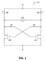
[0018]上述したように、従来の作動XO回路設計は、トランジスタの修正された交差結合対の負のコンダクタンス(−gm)アクティブデバイスとして用いていたし、低周波数でのラッチングを避けるためにハイパスフィルタを追加していた。例えば、図1は従来の差動XO回路100の回路図である。図1において、差動発振は、電界効果トランジスタ(FET)120,122の交差結合対と抵抗を使用して達成される。電源電圧(VDD)が抵抗140、142を介して交差結合FETのドレイン端子に結合する。2つの結合キャパシタ130,132がハイパスフィルタリング、故に、ゼロ近似DC利得(close-to-zero DC gain)を提供するために追加される。しかし、この構成は、特定の条件の下で発振を提供するよりもラッチアップさせることができた。
[0018] As mentioned above, the conventional working XO circuit design was used as a negative conductance (-gm) active device of a modified cross-coupled pair of transistors and a high pass filter to avoid latching at low frequencies Was added. For example, FIG. 1 is a circuit diagram of a conventional
[0019]ここに説明されている複数の実施形態は、差動XO回路を提供するために異なる構成を使用する。一実施形態において、トランジスタの交差結合対が、主発振デバイスとして使われる。低周波数でのラッチングを避けるために、フィードバックループに抵抗を有する金属酸化物半導体電界効果トランジスタ(MOSFET)ダイオードが、トランジスタの交差結合対の各分岐に追加される。低周波数では、MOSFETダイオードは低インピーダンス負荷(1/gm)として作用し、それはループ利得を減じ、ラッチングを防止する。より高い周波数では、回路のインピーダンスは、MOSFETダイオードのフィードバックループの抵抗の値まで上昇し、ループ利得を増加する。抵抗の値は、より高い周波数で高インピーダンスを提供するように適正に調整されることができる。従って、新規な構成は、XO回路がより少ない付加回路及びより高い振幅(higher swings)で発振を開始し、持続することを可能にする。この説明を読んだ後に、さまざまな実施態様及びアプリケーションで本発明を実施する実視方法が明らかになる。本発明のさまざまな実施態様が本願明細書において記載されているけれども、これらの実施態様が、例えば、一例だけとして提示されており、限定しないことは理解される。このように、さまざまな実施態様のこの詳細な説明は、本発明の範囲又は幅を制限するために解釈されるべきでない。 [0019] The embodiments described herein use different configurations to provide a differential XO circuit. In one embodiment, a cross-coupled pair of transistors is used as the main oscillation device. To avoid low frequency latching, a metal oxide semiconductor field effect transistor (MOSFET) diode with resistance in the feedback loop is added to each branch of the transistor's cross-coupled pair. At low frequencies, the MOSFET diode acts as a low impedance load (1 / gm), which reduces loop gain and prevents latching. At higher frequencies, the impedance of the circuit rises to the value of the MOSFET diode feedback loop resistance, increasing the loop gain. The value of the resistor can be appropriately adjusted to provide high impedance at higher frequencies. Thus, the novel configuration allows the XO circuit to start and sustain oscillation with fewer additional circuits and higher swings. After reading this description, the method of viewing the present invention in various embodiments and applications will become apparent. While various embodiments of the invention have been described herein, it is understood that these embodiments are presented by way of example only and not limitation. Thus, this detailed description of various embodiments should not be construed to limit the scope or breadth of the present invention.
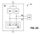
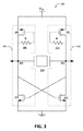
[0020]図2Aは、本発明の一実施形態に従った(差動発振器ドライバ回路250を含む)チップ上に構成される差動XO回路200及び参照共振器230の機能ブロック図である。共振器230は、水晶及び電気石(tourmaline)を含む、様々な共振する結晶物質から形成されることができる。例えば、共振器230は、特定の周波数で共振するように正確にカットされ、寸法づけられ、形成されることができる。一実施形態において、共振器230は水晶共振器である。
[0020] FIG. 2A is a functional block diagram of a
[0021]図2Aの例示の実施形態において、共振器230は、発振器ドライバ回路250の出力端子である一対の端末260、262を介して発振器ドライバ回路250に接続する。共振器230は、差動発振器ドライバ回路250からの好ましくはオフチップに取り付けられる。発振器ドライバ回路250は、第1の部品(part)222及び第2部品224を含む交差結合発振ユニット220及び一対の負荷210、212を含む。第1の部品222は負荷210に結合され、第2の部品224は負荷212に結合される。更に、負荷210、212の対は印加電圧(VDD)に結合され、発振デバイス220は接地電圧に接続される。動作において、差動発振器ドライバ回路250は、差動XO回路200の2つの対称出力端子260、262間に正弦波及び差動出力信号を規定するために特定の周波数で発振するように共振器230を駆動する。正弦波及び差動出力信号は、さまざまなアプリケーション、例えばフェーズロックループ、周波数可変同調型ディジタルフィルタ、直接デジタル周波数合成器及び同様に機能しているデバイスでの使用に適している。
[0021] In the exemplary embodiment of FIG. 2A, the
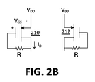
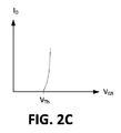
[0022]図2Bに示す実施形態において、対の負荷210、212の各々は、フィードバックループに抵抗(R)を有するMOSFETダイオードとして構成される。抵抗Rのための標準値は、数KΩの範囲内にある。図2Bにおいて、MOSFETダイオード210、212はpチャネルMOSFET(PMOS)ダイオードとして構成され、それらは、PMOSダイオードのゲート端子の電圧が閾値(VTh)を超えると、一方向だけに電流を導通する。図2Cに示すように、閾値(VTh)を超えて、(ID−VGSカーブで反映される)MOSFETダイオードの特性は、二次IV特性を有するダイオードと非常に類似しているように見える。ドレイン電流IDは、次のように表されることができる:
[0022] In the embodiment shown in FIG. 2B, each of the pair of

但し、ID=ドレイン電流;
W/L=幅対長さの比率;
μn=電子移動度;
Cox=単位面積当たりのゲート容量;
VGS=ゲート−ソース間電圧;
VTh=閾値電圧。
Where I D = drain current;
W / L = ratio of width to length;
μ n = electron mobility;
C ox = gate capacitance per unit area;
V GS = gate-source voltage;
V Th = threshold voltage.
[0023]図2Bへ戻って、抵抗(R)は、PMOSダイオードのゲート端子とドレイン端子の間に接続される。PMOSダイオードのソース端子は供給電圧(VDD)に接続される。従って、MOSFETダイオード負荷210、212のインピーダンスは低周波数で低い(1/gm)。その理由は、帰還抵抗(R)が切り離され、高周波でのMOSFETダイオード負荷210、212のインピーダンスが、帰還抵抗(R)の値で高いからである。上記したように、低周波数での負荷の低インピーダンスは、ループ利得を減らし、ラッチングを防止する。更に、より高い周波数での負荷の高インピーダンスは、回路のインピーダンスをフィードバックループの中の抵抗の値まで増加し、かつループ利得を増加する。他の実施形態では、負荷210、212は、NMOSダイオードのソース端子が接地電圧に接続される状態でNMOSダイオードの各々のゲート端子とドレイン端子との間に接続された抵抗(R)を有するn−チャンネルMOSFET(NMOS)として構成されることができる。
[0023] Returning to FIG. 2B, a resistor (R) is connected between the gate and drain terminals of the PMOS diode. The source terminal of the PMOS diode is connected to the supply voltage (VDD). Accordingly, the impedance of the MOSFET diode loads 210 and 212 is low (1 / g m ) at low frequencies. The reason is that the feedback resistor (R) is disconnected, and the impedance of the MOSFET diode loads 210 and 212 at a high frequency is high at the value of the feedback resistor (R). As described above, the low impedance of the load at low frequencies reduces the loop gain and prevents latching. Furthermore, the high impedance of the load at higher frequencies increases the circuit impedance to the value of the resistance in the feedback loop and increases the loop gain. In other embodiments, the
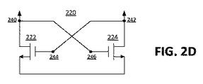
[0024]図2Dに示された実施形態において、主発振デバイス220が、トランジスタ222、224の交差結合対として構成される。この実施形態では、第1のトランジスタのゲート端子244が第2のトランジスタ224のドレイン端子242に接続されるが、第2のトランジスタ224のゲート端子は第1のトランジスタ222のドレイン端子240に接続される。図2Dの例示の実施形態において、トランジスタ222、224の交差結合対は、NMOSトランジスタで構成される。
[0024] In the embodiment shown in FIG. 2D, the main
[0025]図3は、本発明の一実施形態に従った2つの分岐350、352によって構成される差動XO回路300のブロック線図である。図3の例示の実施形態において、NMOSトランジスタ310、312の交差結合対は、第1の分岐350の第1のトランジスタ310及び第2の分岐352の第2トランジスタ312によって差動構成に配置される。第1のトランジスタ310のゲート端子は第2トランジスタ312のドレイン端子に接続されるが、第2のトランジスタ312のゲート端子は第1のトランジスタ310のドレイン端子に接続される。オフチップ参照共振器330は第1及び第2のトランジスタ310、312のドレイン端子に接続される。更に、第1の分岐350では、第1のトランジスタ310のドレイン端子が、第1のPMOSダイオード320のドレイン端子に接続され、それはゲート端子とドレイン端子間のフィードバックループ内に値Rを有する抵抗340を含む。対応して、第2の分岐352において、第2のトランジスタ312のドレイン端子が、第2のPMOSダイオード322のドレイン端子に接続され,それはゲート端子とドレイン端子間のフィードバックループ内に値Rを有するレジスタ342を含む。
[0025] FIG. 3 is a block diagram of a
[0026]図3において、第1の分岐に対して、第1のPMOSダイオード320は、低周波数では低インピーダンス負荷(1/gm)として作用し、より高い周波数では高インピーダンス負荷(R)として作用する。第2の分岐に対して、第2のPMOSダイオード322は、低周波数では低インピーダンス負荷(1/gm)として作用し、より高い周波数では高インピーダンス負荷(R)として作用する。動作において、PMOSダイオード320のゲート端子の電圧が閾値電圧を上回ると、電源が電流をPMOSダイオード320のソース端子に及びドレイン端子までに供給する。更に、PMOSダイオード322のゲート端子の電圧が閾値電圧を上回ると、電源がPMOSダイオード322のソース端子に及びドレイン端子まで電流を供給する。PMOSダイオード320、322のゲート端子の電圧は、参照共振器330の発振電圧によって決定される。図3に示される実施形態において、トランジスタ310、312はNMOSトランジスタによって構成されるけれども、トランジスタ310、312はPMOSトランジスタによって構成されることができる。
[0026] In FIG. 3, for the first branch, the
[0027]ノード360は、参照共振器330の1つの端子、第1のNMOSトランジスタ310のドレイン端子及び第1のPMOSダイオード320のドレイン端子を接続する。更に、ノード362は参照共振器330の他の端子、第2のNMOSトランジスタ312のドレイン端子及び第2のPMOSダイオード322のドレイン端子を接続する。第1及び第2のPMOSダイオード320、322のソース端子は、供給電圧(VDD)に共に接続されているが、第1及び第2のNMOSトランジスタ310、312のソース端子は接地電圧に共に接続されている。
[0027] The
[0028]図4は、本発明の他の実施形態に従った差動XO回路400の概略図である。図4の図示実施形態において、電流源450はPMOSダイオード420、422に適当量の電流を供給するために追加される。従って、PMOSダイオード420のゲート端子の電圧が閾値電圧を上回ると、電流源450がPMOSダイオード420のソース端子に及びドレイン端子まで電流を供給する。更に、PMOSダイオード422のゲート端子の電圧が閾値電圧を上回ると、電流源450がPMOSダイオード422のソース端子に及びドレイン端子まで電流を供給する。PMOSダイオード420、422のゲート端子の電圧は、共振器430の発振電圧によって決定される。
[0028] FIG. 4 is a schematic diagram of a
[0029]図3ですでに述べたように、NMOSトランジスタ410,412の交差結合対は、差動構成に配置され、ここにおいて、第1のトランジスタ410のゲート端子は第2のトランジスタ412のドレイン端子に接続されるが、第2のトランジスタ412のゲート端子は第1のトランジスタ410のドレイン端子に接続される。共振器430は、第1及び第2のトランジスタ410、412のドレイン端子に接続される。ノード460は、参照共振器430の1つの端子、第1のトランジスタ410のドレイン端子及び第1のPMOSダイオード420のドレイン端子を接続する。更に、ノード462は参照共振器430の他の端子、第2のトランジスタ412のドレイン端子及び第2のPMOSダイオード422のドレイン端子を接続する。第1及び第2のPMOSダイオード420、422のソース端子は、電流源450に接続される。
[0029] As already described in FIG. 3, the cross-coupled pair of
[0030]図5は、本発明の更にもう一つの実施形態に従った差動XO回路500の概略図である。図5の図示実施形態において、一対の電流源570、572の各電流源は各分岐550、552に追加されるが、MOSダイオード520、522のインピーダンス負荷はトランジスタ510、512の交差結合対と並列に接続させられた。図5において、MOSダイオード520、522のインピーダンス負荷は、NMOSトランジスタ510、512の交差結合対と並列に接続されたNMOSダイオードとして構成される。
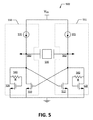
[0030] FIG. 5 is a schematic diagram of a
[0031]NMOSトランジスタの交差結合対510、512は、第2の分岐において第1の分岐550の第1のトランジスタ510及び第2の分岐552の第2のトランジスタ512と差動構成に配置される。第1のトランジスタ510のゲート端子は第2のトランジスタ512のドレイン端子に接続されるが、第2のトランジスタ512のゲート端子は第1のトランジスタ510のドレイン端子に接続される。参照共振器530は、第1及び第2のトランジスタ510、512のドレイン端子に接続される。更に、第1の分岐550において、第1のトランジスタ510のドレイン端子は、第1のNMOSダイオード520のドレイン端子に接続されるが、第1のトランジスタ510のソース端子は第1のNMOSダイオード520のソース端子に接続され、これは、ゲートとドレイン端子の間のフィードバックループの中に値Rを有する抵抗540を含む。このように、第1のトランジスタ510及び第1のNMOSダイオード520は、並列に接続される。上記したように、第1の分岐550に対しては、第1のNMOSダイオード520は、低周波数で低インピーダンス負荷(1/gm)として作用し、及びより高い周波数で高インピーダンス負荷(R)として作用する。対応して、第2の分岐552において、第2のトランジスタ512のドレイン端子は、第2のNMOSダイオード522のドレイン端子に接続されているが、第2のトランジスタ512のソース端子が第2のNMOSダイオード522のソース端子に接続され、それは、ゲートとドレイン端子の間のフィードバックループの中に値Rを有する抵抗器542を含む。このように、第2のトランジスタ512及び第2のNMOSダイオード522は、並列に接続される。第2のNMOSダイオード522は、第2の分岐552に対して、低周波数で低インピーダンス負荷(1/gm)として作用し、より高い周波数で高インピーダンス負荷(R)として作用する。
[0031] The NMOS transistor
[0032]ノード560は、参照共振器530の1つの端子、第1のトランジスタ510のドレイン端子及び第1のNMOSダイオード520のドレイン端子を接続する。更に、ノード562は、参照共振器530の他の端子、第1のトランジスタ512のドレイン端子及び第2のNMOSダイオード522のドレイン端子を接続する。第1及び第2のNMOSダイオード520、522のソース端子は、第1及び第2のトランジスタ510、512のソース端子に,及び接地電圧に接続される。
[0032]
[0033]動作において、NMOSダイオード520のゲート端子の電圧が閾値電圧を上回ると、電流源570がNMOSダイオード520のドレイン端子に及びソース端子まで電流を供給する。更に、NMOSダイオード522のゲート端子の電圧が閾値電圧を上回ると、電流源572がNMOSダイオード522のドレイン端子に、及びソース端子まで電流を供給する。NMOSダイオード520、522のゲート端子の電圧は、参照共振器530の発振電圧によって決定される。
[0033] In operation, when the voltage at the gate terminal of
[0034]図3、4及び5の差動構成は、低周波数でループ利得を減少し、ラッチングを防止すことによって、及びより高い周波数で回路のインピーダンスを(Rまで)及びループ利得を増やすことによって差動XO回路の従来の設計に勝る相当な利点を提供する。 [0034] The differential configurations of FIGS. 3, 4 and 5 reduce loop gain at low frequencies, prevent latching, and increase circuit impedance (to R) and loop gain at higher frequencies. Provides considerable advantages over conventional designs of differential XO circuits.
図6は、本発明の一実施形態に従った差動発振回路の出力端子で発振周波数を発生するための方法600を例示している機能的なフロー図である。一実施形態において、ステップ610では、トランジスタ310、312の交差結合対及び差動発振回路300の出力端子360、362の間に結合した参照共振器330を用いて、差動発振周波数が発生される。トランジスタ310、312の差動結合対が、差動構成に配置され、ここにおいて、第1のトランジスタ310のゲート端子は、第2のトランジスタ312のドレイン端子に接続されるが、第2のトランジスタ312のゲート端子が第1のトランジスタ310のドレイン端子に接続される。一実施形態において、参照共振器330は、通常、差動発振回路からオフチップに配置されるように構成される。ステップ620では、低インピーダンス負荷が、トランジスタ310、312の交差結合対に結合される一対のMOSFETダイオード320、322によって低周波数で生成される。低周波数での低インピーダンス負荷は、非常に小さい値である相互コンダクタンス(1/gm)の逆数(inverse)である。ステップ630では、高インピーダンス負荷が、トランジスタ310、312の交差結合対に結合されるMOSFETダイオード320、322の同じ対によってより高い周波数で生成される。より高い周波数での高インピーダンス負荷は、ゲートとドレイン端子との間における、MOSFETダイオードのフィードバックの中の抵抗(R)の値である。抵抗の値Rは、高インピーダンス負荷を提供するように調整されなければならない。
FIG. 6 is a functional flow diagram illustrating a
[0035]本発明の幾つかの実施形態が上記に説明されているが、本発明の多くのバリエーションが可能である。例えば、図示の実施形態は、低及び高周波数負荷の両方を提供するとしてMOSFETダイオードを示しているが、2つの差動周波数に対して適正な負荷を提供する回路の幾つかの構成が使用されることができる。更に、さまざまな実施形態の特徴は、上述したものとは異なる組合せで組み合わせることができる。更に、明白で簡単な説明のために、システム及び方法の多くの記述が簡略化されている。多くの説明は、特定の標準の用語及び構造を使用する。しかし、開示されたシステム及び方法は、広くより適用できる。 [0035] Although several embodiments of the invention have been described above, many variations of the invention are possible. For example, although the illustrated embodiment shows a MOSFET diode as providing both low and high frequency loads, several configurations of circuits that provide proper loading for two differential frequencies are used. Can. Further, the features of the various embodiments may be combined in different combinations than those described above. Moreover, many descriptions of systems and methods have been simplified for clarity and simplicity. Many descriptions use specific standard terms and structures. However, the disclosed systems and methods are more widely applicable.
[0036]当業者は、ここに開示された実施形態に関連して説明された様々な例示的なブロック及びモジュールは、様々な形態で実施され得ることを認識するだろう。幾つかのブロック及びモジュールは、一般にそれらの機能の観点から上述された。そのような機能が、如何に実施されるかは、システム全体に課せられる設計制約に依存する。当業者は、説明された機能性を、各特定のアプリケーションに関して様々な方法で実施できるが、そのような実施の決定は本発明の範囲から逸脱を生じさせるものと解釈されるべきでない。加えて、モジュール、ブロック、又はステップ内の機能のグループ分けは、説明を容易にするためのものである。特定の機能又はステップは、本発明から逸脱することなく1つのモジュール又はブロックから移動され得る。 [0036] Those skilled in the art will appreciate that the various exemplary blocks and modules described in connection with the embodiments disclosed herein can be implemented in various forms. Some blocks and modules have been generally described above in terms of their functionality. How such functions are implemented depends on the design constraints imposed on the entire system. Those skilled in the art can implement the described functionality in a variety of ways for each particular application, but such implementation decisions should not be construed as departing from the scope of the invention. In addition, the grouping of functions within a module, block, or step is for ease of explanation. Certain functions or steps may be moved from one module or block without departing from the invention.
[0037] ここに開示された例に関連して説明された様々な例示的な論理ブロック、モジュール、及び回路は、汎用プロセッサ、デジタルシグナルプロセッサ(DSP)、特定用途向け集積回路(ASIC)、フィールド・プログラマブル・ゲート・アレイ(FPGA)又はその他のプログラマブル論理デバイス、ディスクリートゲート又はトランジスタロジック、ディスクリート・ハードウェア・コンポーネント、あるいはここに説明された機能を実行するように設計されたこれらの任意の組み合わせで、インプリメント又は実行されうる。汎用プロセッサは、マイクロプロセッサであることができるが、別の方法では、プロセッサは、任意のプロセッサ、コントローラ、マイクロコントローラ、又はステートマシンであることができる。プロセッサはまた、コンピューティングデバイスの組み合わせ、例えば、DSPと1つのマイクロプロセッサ、複数のマイクロプロセッサ、DSPコアと連携した1つ以上のマイクロプロセッサ、又は任意の他のそのような構成との組み合わせとして実施され得る。更に、本願明細書において記載されている、実施形態を実施する回路及び機能ブロック並びにモジュールは、さまざまなトランジスタ・タイプ、ロジック系統及び設計方法論を用いて実現されることができる。 [0037] Various exemplary logic blocks, modules, and circuits described in connection with the examples disclosed herein may include general purpose processors, digital signal processors (DSPs), application specific integrated circuits (ASICs), fields, and the like. A programmable gate array (FPGA) or other programmable logic device, discrete gate or transistor logic, discrete hardware components, or any combination thereof designed to perform the functions described herein Can be implemented or implemented. A general purpose processor may be a microprocessor, but in the alternative, the processor may be any processor, controller, microcontroller, or state machine. A processor may also be implemented as a combination of computing devices, eg, a combination of a DSP and one microprocessor, multiple microprocessors, one or more microprocessors in conjunction with a DSP core, or any other such configuration. Can be done. Further, the circuits and functional blocks and modules implementing the embodiments described herein can be implemented using various transistor types, logic systems, and design methodologies.
[0038] 開示された実施形態の上記説明は、当業者が本発明を製造又は使用することができるように提供されている。これらの実施形態への様々な修正は、当業者には容易に明らかであるだろうし、ここに説明された一般的な原理は、本発明の精神又は範囲から逸脱しない限り他の実施形態にも適用可能であることができる。従って、ここに提示された説明及び図面は、本発明の現在好ましい実施形態を表し、よって、本発明により広く熟慮される主題事項を代表するものであることは理解されるべきである。更に、本発明の範囲は、当業者に自明になり得る他の実施形態を完全に包含すること、及び、本発明の範囲は従って、添付の特許請求の範囲以外の何によっても限定されないことは理解されるべきである。 [0038] The above description of the disclosed embodiments is provided to enable any person skilled in the art to make or use the present invention. Various modifications to these embodiments will be readily apparent to those skilled in the art, and the generic principles described herein may be practiced in other embodiments without departing from the spirit or scope of the invention. Can be applicable. Accordingly, it is to be understood that the description and drawings presented herein represent presently preferred embodiments of the invention and are therefore representative of subject matter that is widely contemplated by the present invention. Furthermore, the scope of the present invention fully encompasses other embodiments that may be apparent to those skilled in the art, and the scope of the present invention is therefore not limited by anything other than the appended claims. Should be understood.
[0038] 開示された実施形態の上記説明は、当業者が本発明を製造又は使用することができるように提供されている。これらの実施形態への様々な修正は、当業者には容易に明らかであるだろうし、ここに説明された一般的な原理は、本発明の精神又は範囲から逸脱しない限り他の実施形態にも適用可能であることができる。従って、ここに提示された説明及び図面は、本発明の現在好ましい実施形態を表し、よって、本発明により広く熟慮される主題事項を代表するものであることは理解されるべきである。更に、本発明の範囲は、当業者に自明になり得る他の実施形態を完全に包含すること、及び、本発明の範囲は従って、添付の特許請求の範囲以外の何によっても限定されないことは理解されるべきである。
以下に本件出願当初の特許請求の範囲に記載された発明を付記する。
[1] 差動水晶発振回路であって、
第1及び第2の出力端子と、
前記第1及び第2の出力端子に交差結合される第1及び第2のトランジスタを含む交差結合発振ユニットと、
第1及び第2の金属酸化物半導体電界効果トランジスタ(MOSFET)ダイオードと、各MOSFETダイオードはゲートとドレイン端子の間に接続される抵抗を含み、ここにおいて前記第1のMOSFETダイオードは、低周波数で低インピーダンス負荷を、及びより高い周波数で高インピーダンス負荷を前記第1のトランジスタに提供するために前記第1のトランジスタに結合し、前記第2のMOSFETダイオードは、低周波数で低インピーダンス負荷を、及びより高い周波数で高インピーダンス負荷を前記第2のトランジスタに提供するために前記第2のトランジスタに結合し、
発振周波数を確定するために前記第1及び第2の出力端子の間に結合された参照共振器と、
を備える、差動水晶発振回路。
[2] 前記第1及び第2のMOSFETダイオードが第1及び第2のpチャネルMOSFET(PMOS)ダイオードとしてそれぞれ構成される、[1に記載の回路。
[3] 前記第1及び第2のPMOSダイオードのソース端子に、及び供給電圧に結合された電流源を更に備える、[2に記載の回路。
[4] 前記第1及び第2のMOSFETダイオードのソース端子が、供給電圧に結合される、[1]に記載の回路。
[5] 前記第1及び第2のトランジスタが、nチャネルMOSFET(NMOS)トランジスタとして構成される、[1]に記載の回路。
[6] 前記NMOSトランジスタのソース端子が、接地電圧に結合される、[5]に記載の回路。
[7] 前記第1及び第2のMOSFETダイオードのドレイン端子が、前記第1及び第2のトランジスタのドレイン端子に結合される、[1]に記載の回路。
[8] 前記第1及び第2のMOSFETダイオードが、第1及び第2のnチャネルMOSFET(NMOS)ダイオードとしてそれぞれ構成される、[1]に記載の回路。
[9] 前記第1及び第2のNMOSダイオードのソース端子が、前記第1及び第2のトランジスタのソース端子に及び接地電圧に結合される、[8]に記載の回路。
[10] 前記第1及び第2のNMOSダイオードのドレイン端子並びに前記第1及び第2のトランジスタのドレイン端子に結合される第1及び第2の電流源を更に備え、前記第1及び第2の電流源がまた、供給電圧に結合される、[9]に記載の回路。
[11] 差動発振回路の出力端子に発振周波数を発生するための方法であって、前記方法は、
トランジスタの交差結合対及び出力端子の間に結合された参照共振器を使用して発振周波数を発生すること、
前記トランジスタの交差結合対に結合されるMOSFETダイオードを使用して低周波数で低インピーダンス負荷を、及びより高い周波数で高インピーダンス負荷を生成することと、を備え、
前記MOSFETダイオードの各々が、ゲートとドレイン端子の間に接続される抵抗を含む、方法。
[12] 前記MOSFETダイオードと供給電圧の間に電流源を結合することを更に備える、[11の方法。
[13] 接地電圧にトランジスタの交差結合対を結合することを更に備える、[11の方法。
[14] 供給電圧と、前記MOSFETダイオードとトランジスタの前記交差結合対との並列組み合わせとの間に一対の電流源を結合することを更に備える、[11の方法。
[15] 差動発振回路の出力端子に発振周波数を発生するための装置であって、前記装置は、
前記出力端子の間に結合される参照共振器を駆動することによって発振周波数を発生するための手段と、
低周波数で低インピーダンス負荷を、より高い周波数で高インピーダンス負荷を生成するための手段と、
を備え、生成するための手段は、発生するための手段に結合される、装置。
[16] 生成するための前記手段に電流を供給するための手段を更に備える、[11の装置。
[17] 発生するための手段を接地電圧に結合するための手段を更に備える、[11]に記載の装置。
[18] 発生するための前記手段及び生成するための前記手段に電流を供給するための手段を更に備える、[11]に記載の装置。
[0038] The above description of the disclosed embodiments is provided to enable any person skilled in the art to make or use the present invention. Various modifications to these embodiments will be readily apparent to those skilled in the art, and the generic principles described herein may be practiced in other embodiments without departing from the spirit or scope of the invention. Can be applicable. Accordingly, it is to be understood that the description and drawings presented herein represent presently preferred embodiments of the invention and are therefore representative of subject matter that is widely contemplated by the present invention. Furthermore, the scope of the present invention fully encompasses other embodiments that may be apparent to those skilled in the art, and the scope of the present invention is therefore not limited by anything other than the appended claims. Should be understood.
The invention described in the scope of the claims at the beginning of the present application is added below.
[1] A differential crystal oscillation circuit,
First and second output terminals;
A cross-coupled oscillation unit including first and second transistors cross-coupled to the first and second output terminals;
First and second metal oxide semiconductor field effect transistor (MOSFET) diodes, and each MOSFET diode includes a resistor connected between a gate and a drain terminal, wherein the first MOSFET diode has a low frequency A low impedance load is coupled to the first transistor to provide a high impedance load to the first transistor at a higher frequency, and the second MOSFET diode provides a low impedance load at a low frequency, and Coupling to the second transistor to provide a high impedance load to the second transistor at a higher frequency;
A reference resonator coupled between the first and second output terminals to determine an oscillation frequency;
A differential crystal oscillation circuit.
[2] The circuit according to [1], wherein the first and second MOSFET diodes are respectively configured as first and second p-channel MOSFET (PMOS) diodes.
[3] The circuit of [2], further comprising a current source coupled to a source terminal of the first and second PMOS diodes and to a supply voltage.
[4] The circuit of [1], wherein source terminals of the first and second MOSFET diodes are coupled to a supply voltage.
[5] The circuit according to [1], wherein the first and second transistors are configured as n-channel MOSFET (NMOS) transistors.
[6] The circuit according to [5], wherein a source terminal of the NMOS transistor is coupled to a ground voltage.
[7] The circuit according to [1], wherein drain terminals of the first and second MOSFET diodes are coupled to drain terminals of the first and second transistors.
[8] The circuit according to [1], wherein the first and second MOSFET diodes are respectively configured as first and second n-channel MOSFET (NMOS) diodes.
[9] The circuit of [8], wherein source terminals of the first and second NMOS diodes are coupled to source terminals of the first and second transistors and to a ground voltage.
[10] The apparatus further comprises first and second current sources coupled to drain terminals of the first and second NMOS diodes and drain terminals of the first and second transistors. The circuit of [9], wherein the current source is also coupled to a supply voltage.
[11] A method for generating an oscillation frequency at an output terminal of a differential oscillation circuit, the method comprising:
Generating an oscillation frequency using a reference resonator coupled between the cross-coupled pair of transistors and the output terminal;
Generating a low impedance load at a low frequency and a high impedance load at a higher frequency using a MOSFET diode coupled to a cross-coupled pair of transistors,
Each of the MOSFET diodes includes a resistor connected between a gate and a drain terminal.
[12] The method of [11], further comprising coupling a current source between the MOSFET diode and a supply voltage.
[13] The method of [11], further comprising coupling a cross-coupled pair of transistors to a ground voltage.
[14] The method of [11], further comprising coupling a pair of current sources between a supply voltage and a parallel combination of the MOSFET diode and the cross-coupled pair of transistors.
[15] A device for generating an oscillation frequency at an output terminal of a differential oscillation circuit, the device comprising:
Means for generating an oscillation frequency by driving a reference resonator coupled between said output terminals;
Means for generating a low impedance load at a low frequency and a high impedance load at a higher frequency;
And the means for generating is coupled to the means for generating.
[16] The apparatus of [11], further comprising means for supplying current to the means for generating.
[17] The apparatus of [11], further comprising means for coupling the means for generating to a ground voltage.
[18] The apparatus of [11], further comprising means for supplying current to the means for generating and the means for generating.
Claims (18)
第1及び第2の出力端子と、
前記第1及び第2の出力端子に交差結合される第1及び第2のトランジスタを含む交差結合発振ユニットと、
第1及び第2の金属酸化物半導体電界効果トランジスタ(MOSFET)ダイオードと、各MOSFETダイオードはゲートとドレイン端子の間に接続される抵抗を含み、ここにおいて前記第1のMOSFETダイオードは、低周波数で低インピーダンス負荷を、及びより高い周波数で高インピーダンス負荷を前記第1のトランジスタに提供するために前記第1のトランジスタに結合し、前記第2のMOSFETダイオードは、低周波数で低インピーダンス負荷を、及びより高い周波数で高インピーダンス負荷を前記第2のトランジスタに提供するために前記第2のトランジスタに結合し、
発振周波数を確定するために前記第1及び第2の出力端子の間に結合された参照共振器と、
を備える、差動水晶発振回路。 A differential crystal oscillation circuit,
First and second output terminals;
A cross-coupled oscillation unit including first and second transistors cross-coupled to the first and second output terminals;
First and second metal oxide semiconductor field effect transistor (MOSFET) diodes, and each MOSFET diode includes a resistor connected between a gate and a drain terminal, wherein the first MOSFET diode has a low frequency A low impedance load is coupled to the first transistor to provide a high impedance load to the first transistor at a higher frequency, and the second MOSFET diode provides a low impedance load at a low frequency, and Coupling to the second transistor to provide a high impedance load to the second transistor at a higher frequency;
A reference resonator coupled between the first and second output terminals to determine an oscillation frequency;
A differential crystal oscillation circuit.
トランジスタの交差結合対及び出力端子の間に結合された参照共振器を使用して発振周波数を発生すること、
前記トランジスタの交差結合対に結合されるMOSFETダイオードを使用して低周波数で低インピーダンス負荷を、及びより高い周波数で高インピーダンス負荷を生成することと、を備え、
前記MOSFETダイオードの各々が、ゲートとドレイン端子の間に接続される抵抗を含む、方法。 A method for generating an oscillation frequency at an output terminal of a differential oscillation circuit, the method comprising:
Generating an oscillation frequency using a reference resonator coupled between the cross-coupled pair of transistors and the output terminal;
Generating a low impedance load at a low frequency and a high impedance load at a higher frequency using a MOSFET diode coupled to a cross-coupled pair of transistors,
Each of the MOSFET diodes includes a resistor connected between a gate and a drain terminal.
前記出力端子の間に結合される参照共振器を駆動することによって発振周波数を発生するための手段と、
低周波数で低インピーダンス負荷を、より高い周波数で高インピーダンス負荷を生成するための手段と、
を備え、生成するための手段は、発生するための手段に結合される、装置。 A device for generating an oscillation frequency at an output terminal of a differential oscillation circuit, the device comprising:
Means for generating an oscillation frequency by driving a reference resonator coupled between said output terminals;
Means for generating a low impedance load at a low frequency and a high impedance load at a higher frequency;
And the means for generating is coupled to the means for generating.
Applications Claiming Priority (3)
| Application Number | Priority Date | Filing Date | Title |
|---|---|---|---|
| US14/338,241 US9300249B2 (en) | 2014-07-22 | 2014-07-22 | Differential crystal oscillator circuit |
| US14/338,241 | 2014-07-22 | ||
| PCT/US2015/036055 WO2016014176A1 (en) | 2014-07-22 | 2015-06-16 | Differential crystal oscillator circuit |
Publications (2)
| Publication Number | Publication Date |
|---|---|
| JP2017521963A true JP2017521963A (en) | 2017-08-03 |
| JP2017521963A5 JP2017521963A5 (en) | 2018-06-28 |
Family
ID=53490300
Family Applications (1)
| Application Number | Title | Priority Date | Filing Date |
|---|---|---|---|
| JP2017503510A Pending JP2017521963A (en) | 2014-07-22 | 2015-06-16 | Differential crystal oscillation circuit |
Country Status (5)
| Country | Link |
|---|---|
| US (1) | US9300249B2 (en) |
| EP (1) | EP3172835B1 (en) |
| JP (1) | JP2017521963A (en) |
| CN (1) | CN106664058A (en) |
| WO (1) | WO2016014176A1 (en) |
Cited By (3)
| Publication number | Priority date | Publication date | Assignee | Title |
|---|---|---|---|---|
| JP2017155122A (en) * | 2016-03-01 | 2017-09-07 | 日立化成株式会社 | Thermosetting resin composition, prepreg, laminate and printed wiring board |
| JP2018095889A (en) * | 2018-02-14 | 2018-06-21 | 日立化成株式会社 | Resin varnish, prepreg, laminate and printed wiring board |
| JPWO2018105070A1 (en) * | 2016-12-07 | 2018-12-06 | 日立化成株式会社 | Resin varnish, prepreg, laminate and printed wiring board |
Families Citing this family (9)
| Publication number | Priority date | Publication date | Assignee | Title |
|---|---|---|---|---|
| JP5979162B2 (en) * | 2014-01-16 | 2016-08-24 | 株式会社村田製作所 | Power-on reset circuit |
| US9531323B1 (en) | 2015-06-24 | 2016-12-27 | Qualcomm Incorporated | Low-power balanced crystal oscillator |
| US9553545B1 (en) * | 2015-12-29 | 2017-01-24 | Qualcomm Incorporated | Stable differential crystal oscillator with active super diodes |
| CN107947756A (en) * | 2017-11-28 | 2018-04-20 | 中科亿海微电子科技(苏州)有限公司 | Difference CMOS process circuits and oscillatory system |
| CN111342805B (en) * | 2018-12-18 | 2023-12-15 | 天津大学 | Filter unit with impedance curve adjustment module, filter and electronic equipment |
| US10985698B2 (en) | 2019-08-20 | 2021-04-20 | Analog Devices, Inc. | Differential electro-mechanical oscillating circuits and related methods |
| US10763786B1 (en) | 2019-10-28 | 2020-09-01 | Nxp B.V. | Differential crystal oscillator |
| US11177984B1 (en) | 2020-06-01 | 2021-11-16 | Xilinx, Inc. | CMOS analog circuits having a triode-based active load |
| US10998307B1 (en) * | 2020-06-01 | 2021-05-04 | Xilinx, Inc. | CMOS analog circuits having a triode-based active load |
Citations (3)
| Publication number | Priority date | Publication date | Assignee | Title |
|---|---|---|---|---|
| US6696898B1 (en) * | 1998-11-12 | 2004-02-24 | Broadcom Corporation | Differential crystal oscillator |
| US20090206936A1 (en) * | 2008-02-19 | 2009-08-20 | Spectralinear, Inc. | Voltage-controlled oscillator topology |
| JP2012094886A (en) * | 2000-06-22 | 2012-05-17 | Renesas Electronics Corp | Semiconductor integrated circuit |
Family Cites Families (13)
| Publication number | Priority date | Publication date | Assignee | Title |
|---|---|---|---|---|
| AU5299600A (en) * | 1999-05-26 | 2000-12-12 | Broadcom Corporation | Integrated vco |
| US6437652B1 (en) | 2000-12-29 | 2002-08-20 | Broadcom Corporation | Apparatus and method for reducing phase noise in oscillator circuits |
| US6542042B1 (en) | 2001-02-20 | 2003-04-01 | Analog Devices, Inc. | Low power crystal oscillator with feedback resistor pair |
| EP1265352B1 (en) | 2001-06-07 | 2011-08-10 | CSEM Centre Suisse d'Electronique et de Microtechnique S.A. - Recherche et Développement | Differential oscillator circuit comprising an electromechanical resonator |
| US7336138B2 (en) | 2006-04-28 | 2008-02-26 | Renesas Technology Corp. | Embedded structure circuit for VCO and regulator |
| US7391278B2 (en) | 2006-07-31 | 2008-06-24 | Freescale Semiconductor, Inc. | Oscillator with stacked amplifier |
| JP2008252783A (en) | 2007-03-30 | 2008-10-16 | Matsushita Electric Ind Co Ltd | Piezoelectric oscillator |
| EP2289164B1 (en) | 2008-05-30 | 2015-07-08 | Optis Cellular Technology, LLC | Dual-band voltage-controlled oscillator arrangement |
| US7768359B2 (en) | 2008-08-01 | 2010-08-03 | Broadcom Corporation | Low phase noise differential crystal oscillator circuit |
| US8487670B2 (en) * | 2009-09-03 | 2013-07-16 | Qualcomm, Incorporated | Divide-by-two injection-locked ring oscillator circuit |
| JP5900727B2 (en) * | 2011-09-28 | 2016-04-06 | セイコーエプソン株式会社 | OSCILLATOR CIRCUIT, OSCILLATOR, ELECTRONIC DEVICE, AND METHOD FOR STARTING OSCILLATOR |
| US8665030B2 (en) * | 2011-12-14 | 2014-03-04 | Taiwan Semiconductor Manufacturing Company, Ltd. | Voltage-controlled oscillator |
| US8643445B1 (en) | 2012-08-08 | 2014-02-04 | Texas Instruments Incorporated | Crystal oscillator circuit |
-
2014
- 2014-07-22 US US14/338,241 patent/US9300249B2/en active Active
-
2015
- 2015-06-16 EP EP15732148.0A patent/EP3172835B1/en not_active Not-in-force
- 2015-06-16 WO PCT/US2015/036055 patent/WO2016014176A1/en active Application Filing
- 2015-06-16 CN CN201580038394.2A patent/CN106664058A/en active Pending
- 2015-06-16 JP JP2017503510A patent/JP2017521963A/en active Pending
Patent Citations (3)
| Publication number | Priority date | Publication date | Assignee | Title |
|---|---|---|---|---|
| US6696898B1 (en) * | 1998-11-12 | 2004-02-24 | Broadcom Corporation | Differential crystal oscillator |
| JP2012094886A (en) * | 2000-06-22 | 2012-05-17 | Renesas Electronics Corp | Semiconductor integrated circuit |
| US20090206936A1 (en) * | 2008-02-19 | 2009-08-20 | Spectralinear, Inc. | Voltage-controlled oscillator topology |
Cited By (3)
| Publication number | Priority date | Publication date | Assignee | Title |
|---|---|---|---|---|
| JP2017155122A (en) * | 2016-03-01 | 2017-09-07 | 日立化成株式会社 | Thermosetting resin composition, prepreg, laminate and printed wiring board |
| JPWO2018105070A1 (en) * | 2016-12-07 | 2018-12-06 | 日立化成株式会社 | Resin varnish, prepreg, laminate and printed wiring board |
| JP2018095889A (en) * | 2018-02-14 | 2018-06-21 | 日立化成株式会社 | Resin varnish, prepreg, laminate and printed wiring board |
Also Published As
| Publication number | Publication date |
|---|---|
| EP3172835A1 (en) | 2017-05-31 |
| US9300249B2 (en) | 2016-03-29 |
| US20160028349A1 (en) | 2016-01-28 |
| WO2016014176A1 (en) | 2016-01-28 |
| EP3172835B1 (en) | 2018-10-17 |
| CN106664058A (en) | 2017-05-10 |
Similar Documents
| Publication | Publication Date | Title |
|---|---|---|
| JP2017521963A (en) | Differential crystal oscillation circuit | |
| US8872587B2 (en) | Generating negative impedance compensation | |
| US7332977B2 (en) | Crystal clock generator operating at third overtone of crystal's fundamental frequency | |
| US9407201B1 (en) | Crystal oscillator circuit | |
| US20110018646A1 (en) | Lc voltage-controlled oscillator | |
| US7570936B2 (en) | Sub-harmonically pumped mixer | |
| US8643445B1 (en) | Crystal oscillator circuit | |
| JP2017521963A5 (en) | ||
| TWI489767B (en) | Oscillator circuit | |
| US8264290B2 (en) | Dual positive-feedbacks voltage controlled oscillator | |
| TW201310892A (en) | Low noise oscillators | |
| US20060176121A1 (en) | Piezoelectric oscillator having symmetric inverter pair | |
| US20110148534A1 (en) | Lc voltage-controlled oscillator | |
| JP2006510254A (en) | Oscillator circuit that generates high-frequency electromagnetic oscillation | |
| CN107070405B (en) | Oscillator device | |
| CN106374837A (en) | Quadrature voltage controlled oscillator | |
| US7750730B2 (en) | Bandpass filter circuit | |
| US7928810B2 (en) | Oscillator arrangement and method for operating an oscillating crystal | |
| US7397311B2 (en) | Oscillator coupling to reduce spurious signals in receiver circuits | |
| Andriesei et al. | CMOS RF active inductor with improved tuning capability | |
| JP2010219769A (en) | Oscillator circuit and radio set using the oscillator circuit | |
| US20150123714A1 (en) | Highly linear buffer | |
| KR101563805B1 (en) | High frequency signal generator using rf negative resistance circuit with complementary cross-coupled oscillator topology | |
| US20140203880A1 (en) | Bias current circuit and semiconductor integrated circuit | |
| US9231568B2 (en) | Circuit reducing phase noise of oscillator |
Legal Events
| Date | Code | Title | Description |
|---|---|---|---|
| A521 | Request for written amendment filed |
Free format text: JAPANESE INTERMEDIATE CODE: A523 Effective date: 20170403 |
|
| A521 | Request for written amendment filed |
Free format text: JAPANESE INTERMEDIATE CODE: A523 Effective date: 20180521 |
|
| A621 | Written request for application examination |
Free format text: JAPANESE INTERMEDIATE CODE: A621 Effective date: 20180521 |
|
| A871 | Explanation of circumstances concerning accelerated examination |
Free format text: JAPANESE INTERMEDIATE CODE: A871 Effective date: 20181010 |
|
| A975 | Report on accelerated examination |
Free format text: JAPANESE INTERMEDIATE CODE: A971005 Effective date: 20181026 |
|
| A131 | Notification of reasons for refusal |
Free format text: JAPANESE INTERMEDIATE CODE: A131 Effective date: 20181120 |
|
| A02 | Decision of refusal |
Free format text: JAPANESE INTERMEDIATE CODE: A02 Effective date: 20190618 |