JP2017509269A - Combination of amplitude-time modulation and phase modulation - Google Patents
Combination of amplitude-time modulation and phase modulation Download PDFInfo
- Publication number
- JP2017509269A JP2017509269A JP2016562468A JP2016562468A JP2017509269A JP 2017509269 A JP2017509269 A JP 2017509269A JP 2016562468 A JP2016562468 A JP 2016562468A JP 2016562468 A JP2016562468 A JP 2016562468A JP 2017509269 A JP2017509269 A JP 2017509269A
- Authority
- JP
- Japan
- Prior art keywords
- amplitude
- phase
- sine wave
- data
- modulation
- Prior art date
- Legal status (The legal status is an assumption and is not a legal conclusion. Google has not performed a legal analysis and makes no representation as to the accuracy of the status listed.)
- Pending
Links
Images


Classifications
-
- H—ELECTRICITY
- H03—ELECTRONIC CIRCUITRY
- H03C—MODULATION
- H03C5/00—Amplitude modulation and angle modulation produced simultaneously or at will by the same modulating signal
-
- H—ELECTRICITY
- H04—ELECTRIC COMMUNICATION TECHNIQUE
- H04L—TRANSMISSION OF DIGITAL INFORMATION, e.g. TELEGRAPHIC COMMUNICATION
- H04L27/00—Modulated-carrier systems
- H04L27/02—Amplitude-modulated carrier systems, e.g. using on-off keying; Single sideband or vestigial sideband modulation
- H04L27/04—Modulator circuits; Transmitter circuits
-
- H—ELECTRICITY
- H03—ELECTRONIC CIRCUITRY
- H03C—MODULATION
- H03C99/00—Subject matter not provided for in other groups of this subclass
-
- H—ELECTRICITY
- H04—ELECTRIC COMMUNICATION TECHNIQUE
- H04L—TRANSMISSION OF DIGITAL INFORMATION, e.g. TELEGRAPHIC COMMUNICATION
- H04L27/00—Modulated-carrier systems
- H04L27/18—Phase-modulated carrier systems, i.e. using phase-shift keying
- H04L27/20—Modulator circuits; Transmitter circuits
-
- H—ELECTRICITY
- H04—ELECTRIC COMMUNICATION TECHNIQUE
- H04L—TRANSMISSION OF DIGITAL INFORMATION, e.g. TELEGRAPHIC COMMUNICATION
- H04L27/00—Modulated-carrier systems
- H04L27/32—Carrier systems characterised by combinations of two or more of the types covered by groups H04L27/02, H04L27/10, H04L27/18 or H04L27/26
- H04L27/34—Amplitude- and phase-modulated carrier systems, e.g. quadrature-amplitude modulated carrier systems
- H04L27/345—Modifications of the signal space to allow the transmission of additional information
-
- H—ELECTRICITY
- H04—ELECTRIC COMMUNICATION TECHNIQUE
- H04L—TRANSMISSION OF DIGITAL INFORMATION, e.g. TELEGRAPHIC COMMUNICATION
- H04L27/00—Modulated-carrier systems
- H04L27/32—Carrier systems characterised by combinations of two or more of the types covered by groups H04L27/02, H04L27/10, H04L27/18 or H04L27/26
- H04L27/34—Amplitude- and phase-modulated carrier systems, e.g. quadrature-amplitude modulated carrier systems
- H04L27/36—Modulator circuits; Transmitter circuits
-
- H—ELECTRICITY
- H03—ELECTRONIC CIRCUITRY
- H03C—MODULATION
- H03C2200/00—Indexing scheme relating to details of modulators or modulation methods covered by H03C
- H03C2200/0004—Circuit elements of modulators
- H03C2200/0029—Memory circuits, e.g. ROMs, RAMs, EPROMs, latches, shift registers
Abstract
少なくとも1つの振幅−時間変調された正弦波及び少なくとも1つの位相変調された波を含む複合ノッチ正弦波形を生成する1つ又は複数の可変位相変化波形と組み合わせられたエンコードされたデジタル情報を収容する1つ又は複数の実質的正弦波形を有する複合信号波を生成する方法。位相内の波の正弦波振幅に対する変更の存在又は不存在がデータ値を示している。これらのデータ値は、データサイクル又はパケット内において変化させることができる。従来の振幅変調技法と比較された際に、振幅−時間変調技法は、低減された変調歪を提示する。この通信信号における低減された歪は、増大した有効送信長、低減された誤り率、相対的に大きなデータレート、及び改善されたデータセキュリティを結果的にもたらす。Accommodates encoded digital information combined with one or more variable phase change waveforms that generate a composite notch sine waveform including at least one amplitude-time modulated sine wave and at least one phase modulated wave A method of generating a composite signal wave having one or more substantially sinusoidal waveforms. The presence or absence of a change to the sinusoidal amplitude of the wave in phase indicates the data value. These data values can be changed within a data cycle or packet. When compared to conventional amplitude modulation techniques, amplitude-time modulation techniques present reduced modulation distortion. This reduced distortion in the communication signal results in an increased effective transmission length, a reduced error rate, a relatively large data rate, and improved data security.
Description
関連出願の相互参照
本出願は、2014年1月7日付けで出願された「NuSine」という名称の米国仮特許出願第61/924,304号及び2014年12月18日付けで出願された「Combined Amplitude-Time and Phase Modulation」という名称の米国特許出願第14/574,577号の優先権を主張するものであり、これらの特許文献は、いずれも、引用により、そのすべてが本明細書に包含される。
CROSS REFERENCE TO RELATED APPLICATIONS This application is filed on Jan. 7, 2014, US Provisional Patent Application No. 61 / 924,304 entitled "NuSine" and Dec. 18, 2014. No. 14 / 574,577, entitled “Combined Amplitude-Time and Phase Modulation,” which claims priority, all of which are hereby incorporated by reference in their entirety. Is included.
発明の分野
本発明は、概して、データ送信に関し、且つ、更に詳しくは、増大したデータ送信レートを提供する正弦波変調技法に関する。
The present invention relates generally to data transmission, and more particularly to sinusoidal modulation techniques that provide increased data transmission rates.
発明の背景
デジタルデータの送信は、通常、波の振幅、周波数、及び位相からなる特徴的特性のうちの1つ又は複数の特性の変調を通じて、搬送波として利用されている正弦波を変調することにより、ポイントツーポイントで実現されている。
Background of the Invention Transmission of digital data typically involves modulating a sine wave utilized as a carrier wave through modulation of one or more of the characteristic characteristics consisting of the amplitude, frequency, and phase of the wave. Realized point-to-point.
正弦波の振幅変調は、従来、送信対象の供給源との関係において搬送波としての正弦波の振幅を直接的に変化させることにより、実装されている。通常の信号正弦波は、その振幅、周波数、及び位相により、特徴付けられている。正弦波は、異なる媒体からなるホスト上においてデータを送信するべく、使用される。振幅変調(AM:amplitude modulated)されたラジオの場合には、放送される搬送(正弦)波は、音声によって変調されており、且つ、簡単なAM受信機により、ダイオードによって音声を搬送波信号から分離することが可能であり、音声を増幅することが可能であり、且つ、これをスピーカーを通じて再生することができる。AMラジオは、信号のレンジ、品質、及び信頼性を制限する信号ノイズ副産物という問題点を有する。通常、純粋な正弦波に対する変調又はその他の変更は、高調波、側帯波、及び電磁干渉を含む副産物を生成することになる。 Conventionally, amplitude modulation of a sine wave is implemented by directly changing the amplitude of the sine wave as a carrier wave in relation to a transmission source. A normal signal sine wave is characterized by its amplitude, frequency, and phase. A sine wave is used to transmit data on a host of different media. In the case of an amplitude-modulated (AM) radio, the broadcast carrier (sine) wave is modulated by sound, and a simple AM receiver separates the sound from the carrier signal by a diode. It is possible to amplify the sound and reproduce it through the speaker. AM radio has the problem of signal noise by-products that limit the range, quality, and reliability of the signal. Typically, modulation or other changes to a pure sine wave will produce by-products including harmonics, sidebands, and electromagnetic interference.
搬送波としての正弦波の直接的な変調は、フィルタリングが困難な大きなノイズを生成する。周波数変調技法は、通常、波の瞬間的な周波数を変化させて搬送波としての正弦波内において情報をエンコードすることにより、実装されている。位相変調技法は、通常、搬送波の瞬間的な位相の変動によって搬送波としての正弦波上において情報をエンコードすることにより、実装されている。 Direct modulation of a sine wave as a carrier generates large noise that is difficult to filter. Frequency modulation techniques are usually implemented by encoding information in a sinusoid as a carrier by changing the instantaneous frequency of the wave. Phase modulation techniques are typically implemented by encoding information on a sine wave as a carrier by instantaneous phase variations of the carrier.
ハイブリッド型の変調方式も開発されており、これには、QAM、SM、及びSSBが含まれる。これらの確立されたハイブリッド型変調方式は、データ送信を改善してはいるが、依然として、実際の送信レートを低減する大きなノイズ及びその他の変調副産物という問題点を有しており、且つ、過剰なスペクトルリソースを使用する。 Hybrid modulation schemes have also been developed, including QAM, SM, and SSB. Although these established hybrid modulation schemes improve data transmission, they still have the problem of large noise and other modulation by-products that reduce the actual transmission rate, and excessive Use spectrum resources.
従って、データの波変調エンコーディングにおける改善が求められている。 Therefore, there is a need for improvements in wave modulation encoding of data.
発明の概要
以下、本発明が従来技術の欠点に対処する方法について更に詳細に説明することとするが、一般に、本発明は、大幅に改善された信号対ノイズ比(即ち、チャネルのノイズエネルギーに対するデータによって生成されるエネルギー)、低減された帯域幅要件、所与のビット誤り率(BER:bit error rate)におけるデータ回復における増大したノイズ耐性、及び変調プロセスの改善された動的制御を提供する新しい変調技法を提供する。
SUMMARY OF THE INVENTION In the following, the method by which the present invention addresses the shortcomings of the prior art will be described in more detail. Provides energy generated by data), reduced bandwidth requirements, increased noise immunity in data recovery at a given bit error rate (BER), and improved dynamic control of the modulation process Provide new modulation techniques.
位相−振幅−時間変調は、従来の変調方法/技法との比較において、データ送信レートの大幅な増大を提供する。この新しい技法は、任意の周波数及び大部分の既存の有線及び無線通信インフラストラクチャに対して適用することができる。 Phase-amplitude-time modulation provides a significant increase in data transmission rate in comparison to conventional modulation methods / techniques. This new technique can be applied to any frequency and most existing wired and wireless communication infrastructures.
本発明の一態様は、いくつかの実施形態において、位相0における送信のために正弦波を生成するステップと、ピーク及びゼロ交差位相からの更なる1つ又は複数の波送信を制限するステップと、可変非制限位相において少なくとも1つの更なる正弦波を生成するステップと、振幅−時間変調の歪を通じて正弦波のうちの1つ又は複数を歪ませてデジタル情報をエンコードするステップと、振幅−時間変調を通じて、正弦波の歪においてビットコンテンツ1〜nをエンコードするステップと、を含むデジタルデータをエンコードする方法を提供している。
One aspect of the invention, in some embodiments, generates a sine wave for transmission at
いくつかの実施形態においては、方法は、1サイクル内において、密度1〜nにおいて、位相シフトされた正弦波を送信するステップを含む。 In some embodiments, the method includes transmitting a phase shifted sine wave at a density of 1 to n within one cycle.
いくつかの実施形態においては、方法は、正弦波振幅の位相変動歪からデジタル情報をデコードするステップを含む。 In some embodiments, the method includes decoding the digital information from a sinusoidal amplitude phase variation distortion.
いくつかの実施形態においては、振幅−時間変調の歪は、短期間にわたって正弦波の振幅を維持するか又は最小限に遅延させるステップのうちの少なくとも1つを介して実現される。 In some embodiments, amplitude-time modulation distortion is achieved through at least one of maintaining or minimally delaying the amplitude of the sine wave over a short period of time.
いくつかの実施形態においては、正弦波の振幅−時間変調の歪は、正弦波上におけるステップ(段)を近似している。 In some embodiments, the amplitude-time modulation distortion of a sine wave approximates a step on the sine wave.
いくつかの実施形態においては、方法は、データ値と制御メッセージのうちの1つを正弦波のうちの1つの正弦波の位相シフトとしてエンコードするステップを含む。いくつかの実施形態においては、位相シフトは、変調の向きの反転、最上位ビット(MSB:most significant bit)の位置の反転、データビット場所の予め定義されたフォーマッティング、及びシンボル用の更なるデータビットの表現のうちの1つ又は複数を示している。 In some embodiments, the method includes encoding one of the data value and the control message as a phase shift of one of the sine waves. In some embodiments, the phase shift includes inversion of modulation direction, inversion of most significant bit (MSB) position, pre-defined formatting of data bit locations, and additional data for the symbol. One or more of the bit representations are shown.
いくつかの実施形態においては、正弦波のうちの1つ又は複数の正弦波の振幅及び位相成分は、互いに直交した状態において送信されている。 In some embodiments, the amplitude and phase components of one or more of the sine waves are transmitted orthogonal to each other.
いくつかの実施形態においては、方法は、正弦波を合計するステップと、正弦波を変換するステップと、正弦波を送信するステップと、を含む。いくつかの実施形態においては、方法は、正弦波を受け取るステップと、正弦波からデジタル情報を暗号解読するステップと、を含む。 In some embodiments, the method includes summing the sine waves, converting the sine waves, and transmitting the sine waves. In some embodiments, the method includes receiving a sine wave and decrypting the digital information from the sine wave.
本発明の別の態様は、いくつかの実施形態においては、正弦波上においてデジタルデータをエンコードするシステムを提供している。システムは、正弦波を生成するように構成された生成器回路と、ピーク及びゼロ交差位相からの可変波送信を制限すると共に、制限されていない位相において可変波送信を生成するように構成されたコントローラ/カウンタ回路と、正弦波の振幅−時間変調を歪ませることにより、1サイクル内において、1〜nのビットコンテンツにより、デジタル情報をエンコードするように構成されたコントローラ/遅延回路と、第1正弦波を可変位相シフト正弦波を用いて複合正弦波として合計するように構成された合計回路と、送信のために複合正弦波を変換するように構成されたアップコンバータ回路と、複合正弦波を送信するように構成されたフロントエンド回路と、を含む。 Another aspect of the invention provides a system for encoding digital data on a sinusoid in some embodiments. The system is configured to generate a variable wave transmission in an unrestricted phase with a generator circuit configured to generate a sine wave, and to limit variable wave transmission from peak and zero crossing phases A controller / counter circuit, a controller / delay circuit configured to encode digital information with 1 to n bit contents in one cycle by distorting the amplitude-time modulation of the sine wave; A summing circuit configured to sum the sine wave as a composite sine wave using a variable phase shift sine wave, an upconverter circuit configured to convert the composite sine wave for transmission, and a composite sine wave And a front end circuit configured to transmit.
いくつかの実施形態においては、システムは、複合正弦波からデジタルデータをデコードするように構成されたダウンコンバータ回路を含む。 In some embodiments, the system includes a downconverter circuit configured to decode digital data from the composite sine wave.
いくつかの実施形態においては、コントローラ/遅延回路は、波の位相を遅延させて正弦波の振幅−時間歪を生成するように構成されている。いくつかの実施形態においては、正弦波の振幅−時間歪は、波シグネチャにおけるステップとして示されている。 In some embodiments, the controller / delay circuit is configured to delay the phase of the wave to produce a sinusoidal amplitude-time distortion. In some embodiments, the amplitude-time distortion of the sine wave is shown as a step in the wave signature.
いくつかの実施形態においては、コントローラ/カウンタ回路は、正弦波に沿った既定の位相場所期間において複数の正弦波搬送波1〜nを生成するように構成されている。 In some embodiments, the controller / counter circuit is configured to generate a plurality of sine wave carriers 1-n in a predetermined phase location period along the sine wave.
本発明の別の態様は、いくつかの用途において、正弦波の振幅−時間変調と可変位相変調を組み合わせた変調方法を提供している。振幅−時間変調は、正弦波振幅のわずかな位相変動歪を通じてレガシー変調技法が提示するスプリアス放出の大部分を回避する。いくつかの実装形態においては、振幅−時間変調は、振幅−時間変調において正弦波に対するステップ又はポーチ様の位相変化として示されるわずかなビット当たりの変化に基づいたステップ−ポーチ歪として表現されている。 Another aspect of the invention provides a modulation method that combines sinusoidal amplitude-time modulation and variable phase modulation in some applications. Amplitude-time modulation avoids most of the spurious emissions that legacy modulation techniques present through slight phase variation distortion of sinusoidal amplitude. In some implementations, the amplitude-time modulation is expressed as a step-pouch distortion based on a slight bit-by-bit change that is shown as a step or pouch-like phase change for a sine wave in the amplitude-time modulation. .
レガシー変調方式は、通常、ノイズ及びその他の変調副産物に起因し、わずかな数の情報ビット/サイクルに制限されている。対照的に、振幅−時間変調は、1〜nビット/サイクルの能力を有しており、nは、通信ハードウェア装置アーキテクチャ並びにピーク及び交差位相によってのみ制限されている。それぞれのn個のビットの集合体は、それぞれの波の設定された位相角において配置されたビットの組を含み得る。更には、振幅−時間変調の低減されたノイズシグネチャにより、相対的に多くのビット/サイクルを送信することができる。通常、「0」値のビットは、正弦波の値の変化がないことにより、表され、且つ、「1」値のビットは、波上の所与の位置における正弦波振幅を(わずかに)増大又は減少させることにより、表される。交互に変化するビットの反転及び適応型の変更などの従来のエンコーディング技法を振幅−時間変調に対して適用してもよい。 Legacy modulation schemes are usually limited to a small number of information bits / cycle due to noise and other modulation by-products. In contrast, amplitude-time modulation has a capability of 1 to n bits / cycle, where n is limited only by the communication hardware device architecture and peak and cross phase. Each collection of n bits may include a set of bits arranged at a set phase angle of each wave. Furthermore, a relatively large number of bits / cycles can be transmitted with a reduced noise signature of amplitude-time modulation. Normally, a bit with a “0” value is represented by no change in the value of the sine wave, and a bit with a “1” value indicates (slightly) the sine wave amplitude at a given position on the wave. Expressed by increasing or decreasing. Conventional encoding techniques such as alternating bit inversion and adaptive change may be applied to amplitude-time modulation.
低減されたノイズとの間における振幅−時間変調の組合せによれば、可変位相シフト信号の密度を増大させることが可能であり、且つ、複数の正弦波搬送波1〜nを正弦波に沿った既定の位相場所期間において配置することができる。配置は、波上の任意の場所におけるものであってもよく、ここで、nの値は、例えば、装置ハードウェアアーキテクチャ、ピーク及び交差位相、並びに、クロック速度に依存している。正弦波の可変位相変調の追加を実装することにより、送信におけるデータコンテンツを増大させることができる。可変位相変調データは、更なるデータビット及び/又は制御ビットを促進することにより、所与の帯域幅において送信されるデータの量及びセキュリティを改善することもできる。
The combination of amplitude-time modulation with reduced noise makes it possible to increase the density of the variable phase-shifted signal and to set a plurality of
通信を目的として、振幅−時間変調された正弦波を1〜n次の1つ又は複数の可変位相変調正弦波と組み合わせることにより、複合信号波を形成する。複合信号波は、ほとんどの任意の形態の通信システム上において、フォーマット、変調、及び送信することができる。次いで、複合信号波は、通常の通信データとして、復調及び暗号解読することができる。有線及び無線通信システムのあらゆる組合せが、位相−振幅−時間変調技法の利益を享受し得る。 For communication purposes, a composite signal wave is formed by combining an amplitude-time modulated sine wave with one or more variable phase modulated sine waves of 1 to n order. The composite signal can be formatted, modulated, and transmitted over almost any form of communication system. The composite signal wave can then be demodulated and decrypted as normal communication data. Any combination of wired and wireless communication systems can benefit from phase-amplitude-time modulation techniques.
位相−振幅−時間変調は、リスト及びルックアップテーブルを利用した従来の電子ハードウェアと共に、且つ、様々な用途におけるカスタム装置又はソフトウェアソリューションと共に、利用することができる。 Phase-amplitude-time modulation can be used with conventional electronic hardware using lists and look-up tables, and with custom equipment or software solutions in various applications.
従って、開示されている位相−振幅−時間変調技法は、大幅に改善された信号対ノイズ比、低減された帯域幅要件、増大したノイズ耐性、及び変調プロセスの改善された制御を提供する。 Thus, the disclosed phase-amplitude-time modulation technique provides a greatly improved signal to noise ratio, reduced bandwidth requirements, increased noise immunity, and improved control of the modulation process.
図面の簡単な説明
添付図面との関連における検討の際に詳細な説明及び請求項を参照することにより、本発明について更に十分に理解することができよう。
BRIEF DESCRIPTION OF THE DRAWINGS The invention may be more fully understood by reference to the detailed description and claims when considered in connection with the accompanying drawings.
詳細な説明
以下の説明は、本発明の例示用の実施形態に関するものに過ぎず、且つ、本発明の範囲、適用可能性、又は構成の限定を意図したものではない。むしろ、以下の説明は、本発明の様々な実施形態を実装するための便利な例示を提供することを意図している。明らかになるように、本明細書において記述されている本発明の範囲を逸脱することなしに、これらの実施形態において記述されている要素の機能及び構成において様々な変更が実施され得る。本明細書における説明は、異なるコンポーネント、変調/復調メカニズム、及びこれらに類似したものを有する代替構成の装置と共に利用されるように適合されてもよく、且つ、依然として本発明の範囲に含まれ得ることを理解されたい。従って、本明細書における詳細な説明は、限定ではなく、例示を目的として提示されるものに過ぎない。
DETAILED DESCRIPTION The following description relates only to exemplary embodiments of the invention and is not intended to limit the scope, applicability, or configuration of the invention. Rather, the following description is intended to provide a convenient illustration for implementing various embodiments of the invention. As will become apparent, various changes may be made in the function and arrangement of the elements described in these embodiments without departing from the scope of the invention described herein. The description herein may be adapted to be used with alternative components having different components, modulation / demodulation mechanisms, and the like, and may still be within the scope of the present invention. Please understand that. Accordingly, the detailed description herein is presented for purposes of illustration and not limitation.
「一実施形態」又は「1つの実施形態」に対する本明細書における参照は、その実施形態との関連において記述されている特定の特徴、構造、又は特性が、本発明の少なくとも1つの実施形態に含まれていることを示すことを意図したものである。本明細書の様々な場所における「一実施形態においては」又は「1つの実施形態」というフレーズの出現は、必ずしも、そのすべてが、その同一の実施形態を参照しているというわけではない。 References herein to “one embodiment” or “one embodiment” refer to a particular feature, structure, or characteristic described in connection with that embodiment, in at least one embodiment of the invention. It is intended to show that it is included. The appearances of the phrases “in one embodiment” or “in one embodiment” in various places in the specification are not necessarily all referring to the same embodiment.
本発明の様々な態様によれば、正弦波の位相−振幅−時間変調は、低減されたノイズ及び増大したデータ密度を提供する。本発明は、通信システム上における送信のためにデータを効率的にエンコードするべく使用されてもよい。 In accordance with various aspects of the present invention, sinusoidal phase-amplitude-time modulation provides reduced noise and increased data density. The present invention may be used to efficiently encode data for transmission over a communication system.
図1を参照すれば、わずかな歪を有するデジタル的に合成された正弦波が示されており、この正弦波上においては、データストリーム内におけるデータビットの存在又は不存在によって特徴付けられたステップ関数を使用することにより、データが印加又はエンコードされている。デジタル情報は、ステップ−ポーチ型の波の歪として示される振幅−時間変調を通じて、エンコードすることができる。様々な実施形態においては、このステップ関数は、振幅−時間変調(「ATM」)又はATM成分と呼称される。情報をエンコードするステップ−ポーチ歪は、レガシーAM信号との比較において、信号歪を軽減する。低減された歪の更なる利益には、相対的に大きなワードワイズ(1〜n)、相対的に大きなデータ/サイクル、及び利用可能なスペクトルの効率的な使用が含まれる。 Referring to FIG. 1, a digitally synthesized sine wave with slight distortion is shown on which a step characterized by the presence or absence of data bits in the data stream. Data is applied or encoded by using functions. Digital information can be encoded through amplitude-time modulation, shown as step-pouch-type wave distortion. In various embodiments, this step function is referred to as amplitude-time modulation (“ATM”) or ATM component. Step-pouch distortion encoding information reduces signal distortion in comparison to legacy AM signals. Additional benefits of reduced distortion include relatively large word width (1-n), relatively large data / cycles, and efficient use of available spectrum.
代表的な正弦波は、D−Aコンバータ上において印加された正弦ルックアップテーブルを使用することにより、生成することができる。 A typical sine wave can be generated by using a sine look-up table applied on the DA converter.
本明細書において記述されている新しい変調技法は、位相−振幅時間変調と呼称される。位相−振幅−時間変調は、信号上においてインスタンス生成されたデータがユーザープログラム可能となることを許容する可変位相の直交信号(「位相成分」)を更に導入する。従って、位相−振幅−時間変調は、ATM成分及び位相成分の観点において記述することができる。 The new modulation technique described herein is referred to as phase-amplitude time modulation. Phase-amplitude-time modulation further introduces a variable phase quadrature signal ("phase component") that allows the instantiated data on the signal to be user programmable. Thus, phase-amplitude-time modulation can be described in terms of ATM components and phase components.
位相−振幅−時間変調における主データチャネルは、ATM変調された正弦波又はATM成分である。通信においては、それぞれのサイクルは、一般に、「シンボル」と呼称される。このチャネル上においては、ATMを使用することにより、16ビット/シンボルのデータレートが実現されているが、技術の更なる発展に伴って、更に大きなデータレートが予想される。ATM変調の向き、即ち、データビットがATM正弦波上において表現される方法は、完全にユーザープログラム可能である。図2及び図3は、1又は0のデータ値を選択的に表し得る選択肢を示している。この場合にも、ビット/シンボルの数値1〜nは、データの場所及び向きと同様に、可変であり、且つ、ユーザー選択可能である。
The main data channel in phase-amplitude-time modulation is an ATM modulated sine wave or ATM component. In communications, each cycle is commonly referred to as a “symbol”. On this channel, a data rate of 16 bits / symbol is realized by using ATM, but with the further development of the technology, a higher data rate is expected. The direction of ATM modulation, ie the way in which data bits are represented on an ATM sine wave, is completely user programmable. 2 and 3 show options that can selectively represent 1 or 0 data values. Also in this case, the
次いで、受信機において、正弦波から、nビットワードの未加工ビットを分離することが可能であり、ピーク及び谷は、プリアンブル又は制御ワード命令によって制御される0及び1のデータビットを表している。向き及びビット/シンボル(サイクル)の数値に加えて、そのサイクルにおけるビットの場所、即ち、ビットが存在している波上における角度も、プログラム可能である。この未加工データは、適宜、正規化、コンディショニング、及び保存することができる。 It is then possible to separate the raw bits of the n-bit word from the sine wave at the receiver, with the peaks and valleys representing the 0 and 1 data bits controlled by the preamble or control word instruction. . In addition to the orientation and bit / symbol (cycle) values, the location of the bit in the cycle, ie, the angle on the wave where the bit exists, is programmable. This raw data can be normalized, conditioned and stored as appropriate.
図4を参照すれば、ATMビットの向きは、エンコード対象の値を表すように選択され得る。関連する受信機は、意図された値を適切に判定するように、この構成について通知され得る。最後に、それぞれの場所におけるATM変調の持続時間も、プログラム可能である。ビット持続時間は、後続のビットの開始点とオーバーラップしない場合があることに留意されたい。 Referring to FIG. 4, the ATM bit orientation may be selected to represent the value to be encoded. The associated receiver can be informed about this configuration to properly determine the intended value. Finally, the duration of ATM modulation at each location is also programmable. Note that the bit duration may not overlap with the starting point of subsequent bits.
次に位相−振幅−時間変調の位相成分の説明に転じれば、実際のデータ値を収容しているATMチャネル/成分とは異なり、位相チャネル/成分は、データ値又は制御メッセージの「表現」である。この位相−振幅−時間変調方式におけるチャネルは、2つの波の合計によるATMチャネルへの位相シフトの導入によって生成されている。この更なるチャネルによれば、更なるデータビットをシンボルに追加するか又はATMチャネルデータのフォーマットに関して制御信号を送信機と受信機との間において送信する方法として、位相シフトの値を使用することができる。従って、位相チャネル成分は、動的に制御可能な物理層変調を可能にしている。例えば、特定の位相シフトの導入により、変調の向きが更なる通知の時点まで反転されることになり、最上位ビット(MSB)の位置が更なる通知の時点まで現時点の構成の反対となり、データビット場所が更なる通知の時点まで予め規定されたフォーマットに変化することになり、ユーザーによって生成されたカスタム構成が更なる通知の時点まで有効となり、又は、更なる位相情報が更なる通知の時点までシンボル用の更なるデータビットを表すことになることを後続のATMチャネル変調が示すことを受信器に対して通知することができよう。 Turning now to the description of the phase components of phase-amplitude-time modulation, unlike ATM channels / components that contain actual data values, phase channels / components are “representations” of data values or control messages. It is. The channel in this phase-amplitude-time modulation scheme is created by introducing a phase shift into the ATM channel by the sum of two waves. According to this further channel, using the value of the phase shift as a way to add further data bits to the symbol or to transmit a control signal between the transmitter and the receiver with respect to the format of the ATM channel data. Can do. Thus, the phase channel component enables dynamically controllable physical layer modulation. For example, with the introduction of a specific phase shift, the modulation direction will be reversed until further notification, the most significant bit (MSB) position will be the opposite of the current configuration until further notification, and the data The bit location will change to a pre-defined format until the time of further notification, and the custom configuration generated by the user will be valid until the time of further notification, or further phase information will be Could indicate to the receiver that the subsequent ATM channel modulation indicates that it would represent further data bits for the symbol.
いくつかの実装形態においては、それぞれのパケット境界における、又はそれぞれのシンボルにおける、変調特性を動的に変更するべく、変調の位相チャネル特性の制御の動的特性を使用することもできよう。 In some implementations, the dynamic characteristics of the modulation phase channel characteristics may be used to dynamically change the modulation characteristics at each packet boundary or at each symbol.
このチャネルによって表されるデータビットの数は、構成に依存することになり、例えば、45度、90度、135度、及び180度のシフトという4つの可能な値への位相チャネルの分割に依存することになる。この使用事例においては、ユーザーは、2つの更なるデータビット/シンボルを、即ち、45°=00、90°=01、135°=10、及び180°=11を追加することができる。これらのビットは、同一のシンボルにおいて、検出され、且つ、ATMチャネル上において送信されるデータに追加される。位相値の可能性が高いほど、許容されるデータビットが多くなることが明らかである。 The number of data bits represented by this channel will depend on the configuration, for example depending on the division of the phase channel into four possible values: 45 degree, 90 degree, 135 degree and 180 degree shifts. Will do. In this use case, the user can add two additional data bits / symbols: 45 ° = 00, 90 ° = 01, 135 ° = 10, and 180 ° = 11. These bits are detected in the same symbol and added to the data transmitted on the ATM channel. It is clear that the higher the likelihood of the phase value, the more data bits that are allowed.
このチャネルは、データバイト、ワード、又はパケットの開始点又は末尾を表す特定のシフトにより、送信されるデータを同期化する手段として使用されてもよい。この結果、その他の変調技法のように、送信を調整するための集約的なプリアンブル制御ビットの送信が不要であることから、相対的に実際的なデータペイロード効率が実現される。これらの様々な特徴の実装形態は、固有の用途要件を充足するためのカスタマイズされたプロプライエタリなプロトコルを生成することができる。この能力は、この技法を利用するシステムの有効データレートにおける更なる利益を生成する。 This channel may be used as a means to synchronize the transmitted data with a specific shift representing the start or end of a data byte, word or packet. As a result, relatively practical data payload efficiency is achieved because there is no need to transmit intensive preamble control bits to adjust the transmission as in other modulation techniques. These various feature implementations can generate customized proprietary protocols to meet unique application requirements. This capability generates additional benefits in the effective data rate of systems that utilize this technique.
図5を参照すれば、ATMチャネルと位相チャネルの関係が示されており、この場合に、位相チャネルは、ATMチャネルとの間において直交した状態にある(90度だけ位相がずれている)。これらの2つの波の値は、独立的にエンコードされる。位相チャネルの位相特性及び振幅特性の組合せは、所与のシンボルのデータ/制御情報を反映している。 Referring to FIG. 5, the relationship between the ATM channel and the phase channel is shown. In this case, the phase channel is orthogonal to the ATM channel (the phase is shifted by 90 degrees). These two wave values are encoded independently. The combination of phase and amplitude characteristics of the phase channel reflects the data / control information for a given symbol.
図6を参照すれば、シンボルエンコーディングの合成されたデータ値は、複合変調信号と呼称される。図4は、この技法によって生成される2つのチャネルを表している。上部のチャネルは、ATM(振幅時間変調)チャネルである。これは、主データチャネルである。これは、図1、図2、及び図3において記述されている変調の存在又は不存在を使用することにより、このデータチャネル上において、1〜n個のデータビット/シンボルをエンコードしている。 Referring to FIG. 6, the combined data value of the symbol encoding is referred to as a composite modulation signal. FIG. 4 represents the two channels generated by this technique. The upper channel is an ATM (amplitude time modulation) channel. This is the main data channel. This encodes 1 to n data bits / symbol on this data channel by using the presence or absence of the modulation described in FIGS. 1, 2 and 3.
下部のチャネルは、位相チャネルである。このチャネルは、更なるビット及び/又は制御ビットを本技術に追加している。位相チャネルの位相及び/又は振幅は、信号上においてエンコードされる望ましい情報又はデータビットを表すべく、変調される。この位相変調と振幅変調の組合せを使用することにより、このチャネル上においてn個の値を表している。このチャネル上におけるビット/シンボルの数値は、エンコード/デコードされるデータ値を生成及び認識するべく十分迅速に応答する送信及び受信回路の能力によって制限されている。 The lower channel is a phase channel. This channel adds additional bits and / or control bits to the technology. The phase and / or amplitude of the phase channel is modulated to represent the desired information or data bits to be encoded on the signal. By using this combination of phase and amplitude modulation, n values are represented on this channel. The number of bits / symbols on this channel is limited by the ability of the transmit and receive circuitry to respond quickly enough to generate and recognize the encoded / decoded data value.
2つのチャネルは、互いに直交した状態にあり、即ち、換言すれば、互いに90度だけ位相がずれている。これらの2つの信号を組み合わせることにより、送信装置から受信装置に送信されるデータ及び/又は制御を収容する複合信号が生成される。 The two channels are in a state of being orthogonal to each other, i.e. in other words, out of phase with each other by 90 degrees. By combining these two signals, a composite signal containing data and / or control transmitted from the transmitting device to the receiving device is generated.
いくつかの実装形態においては、データは、ATMチャネル内においてのみエンコードされてもよく、即ち、位相チャネル上において、位相シフトが00であってもよく、又は、データビットが0であってもよい。 In some implementations, the data may be encoded only within the ATM channel, i.e., the phase shift may be 00 or the data bits may be 0 on the phase channel. .
次に位相−振幅−時間変調された信号の送信の実装形態の説明に転じれば、変調された正弦波は、例えば、3dB圧縮点において、高調波成分を生成するべく、利得ブロックに送信される。このブロックは、ソフトミキサとして機能し、これにより、データレートと正弦波搬送波レートを混合して搬送波の第3、第5、及び第7高調波においてエネルギーを生成する。 Turning now to the description of an implementation of phase-amplitude-time modulated signal transmission, a modulated sine wave is transmitted to the gain block to generate harmonic components, for example, at a 3 dB compression point. The This block functions as a soft mixer, which mixes the data rate with the sinusoidal carrier rate to generate energy at the third, fifth and seventh harmonics of the carrier.
位相−振幅−時間変調技術の別の固有の特徴は、信号が、主には、高調波及びそのAM及びPM成分を使用することにより、送信され得るという点にある。生成された信号エネルギーは、高調波成分周波数においてセンタリングされた帯域通過フィルタを通過する。これは、送信された情報を回復するために必要なAM及びPM鋸歯エネルギー成分を有するスペクトルであることから、高調波以外のすべてがフィルタリングによって除去される。これらの成分は、互いに相補的であり、且つ、同一の時間スロット内において、互いに対称的に反対である。 Another inherent feature of the phase-amplitude-time modulation technique is that the signal can be transmitted primarily by using harmonics and their AM and PM components. The generated signal energy passes through a bandpass filter centered at the harmonic component frequency. Since this is a spectrum with the AM and PM sawtooth energy components necessary to recover the transmitted information, all but the harmonics are filtered out. These components are complementary to each other and are symmetrically opposite each other within the same time slot.
現在使用されている従来の変調の形態は、通常、帯域内又は側帯波エネルギー生成型であり、即ち、生成されるエネルギーは、生成されるノイズ及びその他の副産物と共に、チャネル内において存在している。これは、通常、SNR又はEb/Noの低減をもたらす。 Conventional modulation forms currently in use are typically in-band or sideband energy generation types, i.e., the energy generated is present in the channel along with the generated noise and other by-products. . This usually results in a reduction in SNR or Eb / No.
対照的に、位相−振幅−時間変調は、ほとんど又はまったく帯域内ノイズ生成物を生成せず、その理由は、位相−振幅−時間変調は、スペクトルの高調波部分内のエネルギーを主に使用しているからである。側帯波及び搬送波エネルギーは、すべて、高調波周波数においてセンタリングされた帯域通過フィルタにより、除去される。例えば、搬送波周波数が、100kHzであり、且つ、垂直方向スロープ当たりに9個のビット(又は、ステップ)を有する場合には、データレートは、搬送波レートの18倍、即ち、1.8Mb/sとなる。エネルギーのガウス分布濃縮が、高調波周波数において生成され、且つ、ビットレートにおいて交差する単位値の振幅及び位相を有する。次いで、このエネルギーは、ATM及び位相チャネルの両方の位相及び振幅検出器として機能するように構成されたDSP(digital signal processing:デジタル信号処理)エンジン又は等価な回路実装によって復調される。 In contrast, phase-amplitude-time modulation produces little or no in-band noise product, because phase-amplitude-time modulation mainly uses energy in the harmonic portion of the spectrum. Because. All sideband and carrier energy is removed by a bandpass filter centered at the harmonic frequency. For example, if the carrier frequency is 100 kHz and has 9 bits (or steps) per vertical slope, the data rate is 18 times the carrier rate, ie 1.8 Mb / s. Become. A Gaussian distribution enrichment of energy is generated at harmonic frequencies and has unit values of amplitude and phase that intersect at the bit rate. This energy is then demodulated by a DSP (digital signal processing) engine or equivalent circuit implementation configured to function as a phase and amplitude detector for both ATM and phase channels.
kTBと呼称される理論的ノイズフロア限度は、100kHzの場合に、室温で−124dBmであるが、データのピークパワーは、実際には、−70dBmである。この結果、50dBのRMSを上回るSNRが生成される。 The theoretical noise floor limit, referred to as kTB, is -124 dBm at room temperature at 100 kHz, but the peak power of the data is actually -70 dBm. This results in an SNR greater than 50 dB RMS.
注記:このデータレートは、通常、10e−8のBERの場合に、約100dBのEb/Noを必要とすることになろう。但し、位相−振幅−時間変調は、チャネル内ノイズ又はアーチファクトを生成せず、且つ、差分データビットのみを送信することから、位相−振幅−時間変調は、70dB未満のEb/Noを取得する。 Note: This data rate will typically require about 100 dB Eb / No for a BER of 10e-8. However, since phase-amplitude-time modulation does not generate intra-channel noise or artifacts and transmits only differential data bits, phase-amplitude-time modulation obtains an Eb / No of less than 70 dB.
位相−振幅−時間変調された信号の受信の説明に転じれば、高調波搬送波、即ち、高調波自体、プラス搬送波の周りの関連するエネルギーが、直交検出器に入力される。これは、IQ復調器を生成する、局部発振器において90度の位相シフトを有する二重平衡ミキサのペアを使用することにより、実行することができる。高調波の値によって除算された高調波に局部発振器をロックすることにより、いまや、二重平衡ミキサの、即ち、IQ復調器の、直交及びインシデントポートから到来する時間スロットデータ情報が得られる。位相及び振幅成分が互いに交差している際に、データが反転されているかどうかに応じて、「1」又は「0」が出力される。 Turning to the description of receiving a phase-amplitude-time modulated signal, the harmonic carrier, ie the harmonic itself, the associated energy around the plus carrier, is input to the quadrature detector. This can be done by using a pair of double balanced mixers that have a 90 degree phase shift in the local oscillator to produce an IQ demodulator. By locking the local oscillator to the harmonic divided by the harmonic value, the time slot data information coming from the quadrature and incident ports of the double balanced mixer, ie, the IQ demodulator, is now obtained. When the phase and amplitude components cross each other, “1” or “0” is output depending on whether the data is inverted.
検出器を構成するための別の方法は、搬送波のオリジナルの周波数を取得し、これを二重平衡ミキサに入力し、且つ、同一の周波数において局部発振器ポートにおいてデータを伴わない別の正弦波を入力するというものである。この構成は、差分検出器として機能し、その理由は、二重平衡ミキサのデータ出力は、これら2つの搬送波の差分であるからである。従って、これらの搬送波のいずれか1つにおける任意の位相シフト又は振幅シフトを使用し、データストリームを生成することができる。搬送波及び側帯波成分を破棄し、これにより、ノイズ及びスペクトル要件を低減することができる。この実装形態においては、搬送波の第1グループの高調波歪成分のみが使用されている。複数の正弦波がストリームを通じて伝達される場合には、例えば、通常は上部又は下部正弦波である1つのみが、クロックとして使用される。 Another way to configure the detector is to take the original frequency of the carrier, input it to a double balanced mixer, and generate another sine wave with no data at the local oscillator port at the same frequency. It is to input. This configuration functions as a difference detector because the data output of the double balanced mixer is the difference between these two carriers. Thus, any phase shift or amplitude shift on any one of these carriers can be used to generate the data stream. The carrier and sideband components can be discarded, thereby reducing noise and spectral requirements. In this implementation, only the first group of harmonic distortion components of the carrier are used. If multiple sine waves are transmitted through the stream, for example, only one, usually the upper or lower sine wave, is used as the clock.
マルチチャネル環境においては、高調波のうちの1つのみが送信される。本明細書においては、第3高調波の観点において、いくつかの例が記述されているが、任意の適切な高調波が使用されてもよい。すべての信号が同一位相において始まっている限り、この場合にも、信号が位相コヒーレントである際には、ATMモードと同様に、すべてのチャネルのフレームクロック用に1つの信号を使用することができる。従って、位相−振幅−時間変調においては、使用形態が、単一チャネルから複数チャネルに変化することにより、効率性が向上する。 In a multi-channel environment, only one of the harmonics is transmitted. Although some examples have been described herein in terms of third harmonics, any suitable harmonic may be used. Again, as long as all signals start in the same phase, one signal can be used for all channel frame clocks, as in ATM mode, when the signals are phase coherent. . Therefore, in the phase-amplitude-time modulation, the usage is changed from a single channel to a plurality of channels, thereby improving efficiency.
位相−振幅−時間変調技術の主要な利点の1つは、所与の帯域幅において、現時点の技術よりも多くの情報を通信する能力である。現時点においては、商用の変調形態は、既存の産業標準インフラストラクチャにおいて、約10ビット/ヘルツを実現することができる。レガシー変調技術は、しばしば、情報レート/ヘルツを増大させるために、ビット誤り率を犠牲にしており、産業規格は、約10e−8のビット誤り率(BER 10e−8)を必要としている。 One of the major advantages of phase-amplitude-time modulation techniques is the ability to communicate more information than a current technique in a given bandwidth. At present, commercial modulation formats can achieve about 10 bits / hertz in existing industry standard infrastructure. Legacy modulation techniques often sacrifice bit error rate to increase information rate / hertz, and industry standards require a bit error rate (BER 10e-8) of about 10e-8.
図7は、変調された正弦波搬送波信号を生成するコントローラ/遅延回路又は復調器回路のブロックダイアグラムである。表示されているブロックダイアグラムは、振幅−時間変調を実装するための機能的な基礎である。従来のブロック機能が示されているが、プログラムされたマイクロプロセッサ、デジタル信号プロセッサ、状態機械などのその他の信号処理技法も、このタスクに適している。正弦波ルックアップテーブル(LUT:look up table)がD/Aコンバータを駆動している。位相角0〜360度が、n個の個別の値に量子化されている。マルチビットカウンタが、クロックレートにおいて、これらの個別の値を通じて継続的にカウントしている。マルチビットカウンタの出力は、正弦波関数ルックアップテーブルをアドレス指定しており、正弦波関数ルックアップテーブルは、それぞれの量子化された位相角ごとのデジタルエンコードされた正弦波関数値を提供する。D/Aコンバータが、個別の位相角の正弦波に比例した電圧をルックアップテーブルの入力において出力している。クロック生成器が、遅延要素及びラッチと共に、マルチビットカウンタを駆動するものとして示されており、Highの際の値は、値がLowである際に、トランスペアレントである。この出力がルックアップテーブルを駆動している。ルックアップテーブルは、D/Aコンバータを駆動している。望ましい位相周期を実装する時間インターバルに等しい望ましい数のクロックパルスにわたってルックアップテーブルへの入力を保持することにより、ステップ−ポーチ振幅−時間変調技法を実装した変調。
FIG. 7 is a block diagram of a controller / delay circuit or demodulator circuit that generates a modulated sinusoidal carrier signal. The block diagram shown is the functional basis for implementing amplitude-time modulation. Although conventional block functions are shown, other signal processing techniques such as programmed microprocessors, digital signal processors, state machines, etc. are also suitable for this task. A sine wave look-up table (LUT) drives the D / A converter. The
エンコード対象である情報が、データ入力レジスタに導入されている。データ入力サイズは、装置ハードウェア及びクロック速度に依存したnである。データ入力レジスタは、メモリによってクロッキングされている。データは、予め読み込まれ、且つ、初期データビットが、データ入力レジスタの出力(シリアル)上において出現する。AND関数において出現するのに伴って、カウンタ及びデータ入力レジスタの両方が1の値を収容している場合には、D/Aコンバータの出力は、一定に留まることになる。動作の際に、カウンタは、継続し、且つ、出力は、メモリのコンテンツを順番にアドレス指定する。D/A出力は、カウンタとレジスタの間の値の差が検出された際にのみ、変化することになる。多くの変動を利用することにより、データスループットを極大化させつつ、信号歪を極小化するデジタル情報のエンコーディングを実装することができる。ビットレートコントローラを適応的に構成することにより、通信チャネル状態に適合するようにビットレート又は位相インターバルを変更することができる。更には、ビットレートコントローラは、データ送信用のセキュリティ及び制御機能を実装するように、適合させることもできる。 Information to be encoded is introduced into the data input register. The data input size is n depending on the device hardware and clock speed. The data input register is clocked by the memory. Data is pre-read and initial data bits appear on the output (serial) of the data input register. As it appears in the AND function, if both the counter and the data input register contain a value of 1, the output of the D / A converter will remain constant. In operation, the counter continues and the output addresses the contents of the memory in turn. The D / A output will change only when a value difference between the counter and the register is detected. By utilizing many variations, it is possible to implement encoding of digital information that minimizes signal distortion while maximizing data throughput. By adaptively configuring the bit rate controller, the bit rate or phase interval can be changed to suit the communication channel conditions. Furthermore, the bit rate controller can be adapted to implement security and control functions for data transmission.
図8は、正弦波搬送波信号を通信するための周波数アップコンバータのブロックダイアグラムである。局部発振器が、平衡ミキサの一方の入力を駆動している。変調された正弦波搬送波の組が、平衡ミキサの他方の入力から混合されている。平衡ミキサの出力は、帯域通過フィルタに接続されている。帯域通過フィルタの出力は、適切なドライバ回路を通じて送信される準備が完了した状態にある。 FIG. 8 is a block diagram of a frequency upconverter for communicating a sinusoidal carrier signal. A local oscillator drives one input of the balanced mixer. A set of modulated sinusoidal carriers is mixed from the other input of the balanced mixer. The output of the balanced mixer is connected to a band pass filter. The output of the bandpass filter is ready to be transmitted through an appropriate driver circuit.
図9は、正弦波搬送波信号を伝達するための周波数ダウンコンバータのブロックダイアグラムである。局部発振器が、平衡ミキサの一方の入力を駆動している。受信されたRF入力が、平衡ミキサの他方の入力に混合されている。平衡ミキサの出力は、暗号解読及びコンディショニングのために検出器に対して伝達されている。 FIG. 9 is a block diagram of a frequency down converter for transmitting a sinusoidal carrier signal. A local oscillator drives one input of the balanced mixer. The received RF input is mixed with the other input of the balanced mixer. The output of the balanced mixer is communicated to the detector for decryption and conditioning.
図10は、複合信号波を形成するべく1つに混合される出力を有する個別に変調された正弦波搬送波を特徴とする変調器回路のブロックダイアグラムである。図示のように、1つ又は複数のモジュラー回路(MOD.1、MOD.2、MOD.3、及びMOD.4)は、振幅−時間変調された正弦波搬送波を表している。これらのモジュラー回路は、コンディショニング、送信、及び受信/暗号解読のために、複合波形として混合する加算器/コンバイナに供給されている。加算器/コンバイナの出力は、送信のために、直列又は並列に、データコンボリュータに対して接続されている。可変正弦波搬送波の位置決めは、図4及び図11に示されているように、リスト、ルックアップテーブル、又はソフトウェア制御により、変更することができる。4つのモジュラー回路が示されているが、ハードウェア装置アーキテクチャ及びクロック速度によってのみ制限された状態において、最大でn個の回路を利用し得る。 FIG. 10 is a block diagram of a modulator circuit featuring individually modulated sinusoidal carriers with outputs mixed together to form a composite signal wave. As shown, one or more modular circuits (MOD.1, MOD.2, MOD.3, and MOD.4) represent amplitude-time modulated sinusoidal carriers. These modular circuits are fed into an adder / combiner that mixes as a composite waveform for conditioning, transmission, and reception / decryption. The output of the adder / combiner is connected to the data convolver in series or in parallel for transmission. The positioning of the variable sine wave carrier can be changed by a list, look-up table, or software control, as shown in FIGS. Although four modular circuits are shown, up to n circuits may be utilized, limited only by the hardware device architecture and clock speed.
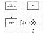
図11は、変調された正弦波から、エンコードされた情報を抽出する復調器回路のブロックダイアグラムである。まず、到来した変調された正弦波搬送波が、入力信号コンディショニングブロックに入力されている。送信のタイプに対して、適宜、様々な信号コンディショニング機能が信号コンディショニングブロック内において使用されることになる。送信のタイプは、限定を伴うことなしに、ツイストペア、無線、マイクロ波、又は差分ラインを含む。信号コンディショニングブロックの出力は、帯域通過フィルタに接続されている。帯域通過フィルタは、通常、100超のQを伴って、搬送波周波数上においてセンタリングされている。帯域通過フィルタからの信号は、Ampブロックによって増幅され、且つ、平衡ミキサブロックに挿入されている。ミキサブロックは、増幅された信号を数値制御発振器であるNCO(numerically controlled oscillator)ブロックと混合している。数値制御発振器の周波数及び位相は、帯域通過フィルタの通過帯域内の振幅−時間変調された正弦波のうちの1つの正弦波の周波数及び位相に対して設定されている。 FIG. 11 is a block diagram of a demodulator circuit that extracts encoded information from a modulated sine wave. First, an incoming modulated sine wave carrier is input to the input signal conditioning block. Depending on the type of transmission, various signal conditioning functions will be used within the signal conditioning block as appropriate. The type of transmission includes, without limitation, twisted pair, radio, microwave, or differential line. The output of the signal conditioning block is connected to a band pass filter. The bandpass filter is typically centered on the carrier frequency with a Q greater than 100. The signal from the band pass filter is amplified by the Amp block and inserted into the balanced mixer block. The mixer block mixes the amplified signal with a numerically controlled oscillator (NCO) block that is a numerically controlled oscillator. The frequency and phase of the numerically controlled oscillator are set with respect to the frequency and phase of one of the amplitude-time modulated sine waves within the passband of the bandpass filter.
図12は、n個の複数の位相変調ストリームを有する復調器回路のブロックダイアグラムである。図示されているのは、通信チャネル内の複数の変調された搬送波であり、エンコードされたデータを暗号解読するべく、それぞれの搬送波の別個の復調が伴っている。6個の平衡ミキサの集合体が示されているが、ハードウェア装置アーキテクチャ及びクロック速度の制限を伴って、n個のミキサを実装することができる。1つ又は複数の入力ラインが、すべての平衡ミキサに供給している。それぞれの平衡ミキサは、数値制御発振器のマルチ周波数正弦波生成器に対する固有の接続を有する。生成器の出力ラインは、搬送波の特定の周波数において、それから抽出されるべき波データを送信する。1つ又は複数のミキサの出力は、搬送波からの情報であり、且つ、こちらも、データコンボリュータに接続されている。データコンボリュータが、1つ又は複数の個々の振幅−時間変調された正弦波信号からのデジタルデータを再アセンブルしている。到来する搬送波は、適合可能な制御情報を利用することにより、異なる周波数及びデータレートを有してもよい。 FIG. 12 is a block diagram of a demodulator circuit having n multiple phase modulated streams. Shown are a plurality of modulated carriers in the communication channel, with separate demodulation of each carrier to decrypt the encoded data. Although a collection of six balanced mixers is shown, n mixers can be implemented with hardware device architecture and clock speed limitations. One or more input lines supply all balanced mixers. Each balanced mixer has a unique connection to the multi-frequency sine wave generator of the numerically controlled oscillator. The generator output line transmits the wave data to be extracted therefrom at a specific frequency of the carrier. The output of one or more mixers is information from the carrier and is also connected to the data convolver. A data convolver reassembles digital data from one or more individual amplitude-time modulated sinusoidal signals. Incoming carriers may have different frequencies and data rates by utilizing adaptable control information.
図13は、振幅−時間エンコーディングを伴う送信/受信通信システムの図である。一例として、RF無線通信のエンドツーエンドのブロックダイアグラムが示されている。それぞれの通信局は、通信機能を制御するためのユーザーインターフェイスを有する。更には、それぞれは、信号のエンコーディング/デコーディングのための変調器/復調器機能を有する。それぞれは、送信/受信される搬送波信号を変調/復調するためのトランシーバも有する。これらの変調通信技法にとっては、任意の最終段のコンディショニング及びトランシーバ機能が適している。 FIG. 13 is a diagram of a transmission / reception communication system with amplitude-time encoding. As an example, an end-to-end block diagram of RF wireless communication is shown. Each communication station has a user interface for controlling communication functions. Furthermore, each has a modulator / demodulator function for signal encoding / decoding. Each also has a transceiver for modulating / demodulating the transmitted / received carrier signal. Any final stage conditioning and transceiver function is suitable for these modulated communication techniques.
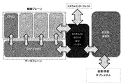
図14は、複合信号波を生成するソフトウェアによって構成可能な方法を実装したインターフェイス回路のブロックダイアグラムである。本ブロックダイアグラムは、ハードウェア機能であり、このハードウェア機能は、大部分の任意の通信システムに適合されるように構成されたソフトウェアであってもよい。インターフェイス回路は、制御プレーンを有するように実装されており、制御プレーンは、GPUによって制御されるIF信号とインターフェイスしたCPU(n個)の集合体である。GPUは、データプレーンを表し、且つ、変換受信及び送信機能を稼働させる。制御プレーン及びデータプレーンは、カスタムI/Oロジック及びバッファを収容したFPGAに対してインターフェイスしている。FPGAも、システムインターフェイスを促進している。FPGAは、信号送信の準備のために、変調器/復調器にもインターフェイスしている。変調器/復調器も、信号送信及び受信機能のために、RFインターフェイスにインターフェイスしている。図示のCPU/GPU実装は、同一機能を実行するようにプログラムされたデジタル信号プロセッサ(DSP)によって置換されてもよい。 FIG. 14 is a block diagram of an interface circuit that implements a method configurable by software that generates a composite signal wave. The block diagram is a hardware function, which may be software configured to be adapted to most arbitrary communication systems. The interface circuit is implemented with a control plane, which is a collection of CPUs (n) that interface with IF signals controlled by the GPU. The GPU represents a data plane and operates conversion reception and transmission functions. The control plane and data plane interface to an FPGA containing custom I / O logic and buffers. FPGAs also promote system interfaces. The FPGA also interfaces with a modulator / demodulator in preparation for signal transmission. The modulator / demodulator also interfaces with the RF interface for signal transmission and reception functions. The illustrated CPU / GPU implementation may be replaced by a digital signal processor (DSP) programmed to perform the same function.
あらゆる変調技術における重要な仕様の1つは、信号対ノイズ比(SNR:signal-to-noise ratio)である。これは、周辺ノイズを上回る、且つ、そのレベルにおいて実現されるBERとの関係においてしばしば表現される、デシベル(DB)を単位として計測された必要とされる信号強度である。換言すれば、ノイズを上回る所与の信号強度の場合に、変調技術は、特定のBERを確実に生成することができる。 One important specification in any modulation technique is the signal-to-noise ratio (SNR). This is the required signal strength measured in decibels (DB), which is often expressed in relation to the BER achieved at that level, above ambient noise. In other words, for a given signal strength above noise, the modulation technique can reliably generate a particular BER.
シンボル誤り率(SER:symbol error rate)は、ビット/シンボルの数値を考慮している。相対的に低いBERを生成するには、相対的に強い信号が必要とされ得る。256QAMのケースにおいては、これは、8ビット/シンボルとなり、従って、SERは、BERを8ビット/シンボルによって除算することによって算出される。相対的に複雑な変調方式は、通常、ノイズの影響を相対的に受けやすい。従って、確実に検出され、且つ、正しく解釈されるためには、信号は、ノイズよりも更に大きくなければならない。受信機が送信された信号を誤って解釈した際には、受信機は、使用されている誤り検出及び補正方式に基づいて、ソフトウェアにおいて、前進型誤り訂正アルゴリズムを実装する可能性があり、且つ、受信機は、送信機によるデータの再送を要求する可能性がある。これらの選択肢は、そのいずれもが、この技術に依存したネットワークの性能に対して悪影響を及ぼす可能性がある。従って、可能な最小のSNRにおいて最小のBERを生成することが有利である。 The symbol error rate (SER) takes into account the number of bits / symbol. To generate a relatively low BER, a relatively strong signal may be required. In the 256QAM case, this is 8 bits / symbol, so SER is calculated by dividing BER by 8 bits / symbol. A relatively complex modulation scheme is usually relatively susceptible to noise. Therefore, in order to be reliably detected and correctly interpreted, the signal must be much larger than the noise. When the receiver misinterprets the transmitted signal, the receiver may implement a forward error correction algorithm in software based on the error detection and correction scheme used, and The receiver may request retransmission of data by the transmitter. Any of these options can adversely affect the performance of networks that rely on this technology. Therefore, it is advantageous to generate the smallest BER at the smallest possible SNR.
QAM(QAM16、QAM64、最大でQAM1024)は、現時点においては、最良の従来型の変調であると見なされているが、その固有の制限は、QAMがアーチファクト及びノイズをチャネル内において生成するという点にある。QAMの場合には、信号を増幅することによって信号対ノイズ比を増大させようとするあらゆる試みは、同一の倍率により、ノイズも増幅する。従って、シャノン限界に常に到達する。従って、最小のQAMステップは、一般に、チャネル内のノイズよりも6dBだけ大きくなければならない。チャネル内にノイズが存在する場合には、ノイズに遭遇する前に、信号を増幅する必要がある。又、実際には、QAMの制限は、その他の既存の形態の変調にも適用されるものであり、その理由は、これらも、帯域内、側帯波、又は関係するコンポーネントタイプの変調を使用しているからである。 QAM (QAM16, QAM64, up to QAM1024) is currently considered the best conventional modulation, but its inherent limitation is that QAM generates artifacts and noise in the channel. It is in. In the case of QAM, any attempt to increase the signal to noise ratio by amplifying the signal will also amplify the noise by the same factor. Therefore, the Shannon limit is always reached. Therefore, the minimum QAM step must generally be 6 dB greater than the noise in the channel. If there is noise in the channel, the signal needs to be amplified before the noise is encountered. In practice, QAM limitations also apply to other existing forms of modulation because they also use in-band, sideband, or related component type modulation. Because.
振幅変調(AM)は、帯域内型であり、且つ、2つの側帯波を有するが、搬送波は不要であり、従って、搬送波と、側帯波のうちの1つと、が、受信機内においてフィルタリングによって除去され、これにより、送信された情報を提供するべく単一の側帯波のみが残される。周波数変調(FM)は、ノイズに対する耐性の観点において、いくつかの利点を有しているが、これは、スペクトルを温存しない。 Amplitude modulation (AM) is in-band and has two sidebands but does not require a carrier, so the carrier and one of the sidebands are filtered out in the receiver. This leaves only a single sideband to provide the transmitted information. Frequency modulation (FM) has several advantages in terms of noise immunity, but it does not preserve the spectrum.
QAMは、一般に、PCM、BPSK、AFSK、及びその他の形態の変調よりも優れていると見なされている。QAMは、正弦波の直交運動と、それぞれの正弦波の振幅ステップと、を利用している。正弦波のレートに応じて、帯域内ノイズ生成効果を伴って、同相において前方又は後方にシフトされたAM成分が存在している。FM又はPMを生成する正弦波の運動に加えて、QAMは、その独自のアーチファクトを有する振幅ステップを利用している。組み合わせられたこれら2つの要素は、チャネルの内部においてランダムノイズを生成する。従って、従来の変調方式は、側帯波又はその他のアーチファクトを生成するデータ搬送方法を利用している。 QAM is generally considered superior to PCM, BPSK, AFSK, and other forms of modulation. QAM uses the orthogonal motion of sine waves and the amplitude steps of each sine wave. Depending on the rate of the sine wave, there is an AM component that is shifted forward or backward in phase with an in-band noise generation effect. In addition to the sinusoidal motion that generates FM or PM, QAM utilizes an amplitude step with its own artifacts. These two elements combined produce random noise inside the channel. Thus, conventional modulation schemes utilize a data transport method that generates sidebands or other artifacts.
例えば、音楽を送信する1MHzのAMラジオ周波数の場合には、ナイキスト限界を破ることなしに、最大で1MHzの半分を、即ち、500KHzを、使用することができる。これを超過した場合には、送信している情報と、情報をその上部において送信している搬送波との間には、スペクトルの差が存在しないことになろう。この限界を超過した場合には、側帯波生成物が生成される。 For example, for a 1 MHz AM radio frequency transmitting music, up to half of 1 MHz, ie 500 KHz, can be used without breaking the Nyquist limit. If this is exceeded, there will be no spectral difference between the information being transmitted and the carrier transmitting the information above it. If this limit is exceeded, a sideband product is generated.
対照的に、位相−振幅−時間変調は、搬送波、側帯波、及びチャネル内外来要素を送信の前に破棄するか又はフィルタリングによって除去している。従って、位相−振幅−時間変調は、16超の数のステップが正弦波上に変調された際に、ナイキスト限界を破る可能性がある。位相−振幅−時間変調の場合には、同一の1MHzの搬送波を使用することにより、16メガビット/秒の第2データレートをサポートし、これにより、ナイキスト限界を抑圧する(例えば、1MHz内において16MHzの搬送波を変調する)ことが可能である。但し、これは、16MHzを有する搬送波ではなく、データストリームである。データストリームは、例えば、101、001、及び010などのいくつかのタイプの周波数のうちの1つであってもよく、最大でチャネル幅限度である更なる組合せを有する。 In contrast, phase-amplitude-time modulation discards the carrier, sidebands, and in-channel extraneous elements before transmission or removes them by filtering. Thus, phase-amplitude-time modulation can break the Nyquist limit when more than 16 steps are modulated onto a sine wave. In the case of phase-amplitude-time modulation, the same 1 MHz carrier is used to support a second data rate of 16 Mbit / s, thereby suppressing the Nyquist limit (eg, 16 MHz within 1 MHz). Can be modulated). However, this is a data stream, not a carrier having 16 MHz. The data stream may be one of several types of frequencies such as 101, 001, and 010, for example, with further combinations that are at most channel width limited.
特定の一実施形態においては、位相−振幅−時間変調された正弦波は、100KHzの搬送波及び数値制御発振器(NCO)を使用することにより、合成されている。例えば、最下位ビット又は最下位ビットの次などに、ビットステップサイズを設定するべく、D−Aコンバータが使用される。「1」、「0」の選択的なトグリングは、ATMと呼称されるステップ又はポーチを正弦波内において生成する。従って、ステップ又はポーチは、1つおきのビット場所及び1つおきの時間スロット場所において生成された「1」又は「0」を表し、従って、それぞれの時間スロットは異なっている。これらのステップ又はポーチは、通常、正弦波の相対的に垂直方向の部分上においてのみ、生成される。例えば、1MHzの正弦波のケースにおいては、垂直方向スロープの相対的に線形の部分のそれぞれごとに8ビットずつ、16個のステップが存在し得る。 In one particular embodiment, a phase-amplitude-time modulated sine wave is synthesized by using a 100 KHz carrier and a numerically controlled oscillator (NCO). For example, a DA converter is used to set the bit step size at the least significant bit or next to the least significant bit. A selective toggle of “1”, “0” creates a step or pouch called ATM in the sine wave. Thus, a step or pouch represents a “1” or “0” generated at every other bit location and every other time slot location, so each time slot is different. These steps or pouches are usually generated only on the relatively vertical portion of the sine wave. For example, in the case of a 1 MHz sine wave, there may be 16 steps, 8 bits for each relatively linear portion of the vertical slope.
8ビット/シンボルのみを有する位相−振幅−時間変調ATMチャネルは、データスループットにおいて、QAM256と等価である。この場合にも、ATMチャネルを使用して送信されるデータは、データの実際の値であり、これは、同一のデータ値を搬送するために2つの変調された波を必要としているQAM256におけるようなデータの表現ではなく、1つの変調された波のみを必要としている。図15は、コンステレーション内のそれぞれのポイントが0〜255の8ビットバイナリ値を表しているQAM256「コンステレーション」を示している。 A phase-amplitude-time modulated ATM channel with only 8 bits / symbol is equivalent to QAM256 in data throughput. Again, the data transmitted using the ATM channel is the actual value of the data, as in QAM256, which requires two modulated waves to carry the same data value. Only one modulated wave is needed rather than a simple data representation. FIG. 15 shows a QAM256 “constellation” where each point in the constellation represents an 8-bit binary value between 0 and 255.
図16を参照すれば、QAM1024コンステレーションマップのそれぞれの象限は、256個の点を収容している。QAM1024の場合には、QAM256に伴って存在している課題が更に顕著になる。例えば、コンステレーション上において、意図された地点を正確に識別し、且つ、その正確なデータ値を判定するには、2つの波が、シンボル周波数において、正確に計測され、且つ、解釈されることを要する。正確性は、システムのBE又はSERを維持するために、受信機の処理を低減するために、又は、更に劣悪なケースにおいては、データ再送信に対するニーズを回避するために、重要である。 Referring to FIG. 16, each quadrant of the QAM1024 constellation map contains 256 points. In the case of QAM1024, the problems that exist with QAM256 become more prominent. For example, on a constellation, two waves are accurately measured and interpreted at the symbol frequency to accurately identify the intended point and determine its exact data value. Cost. Accuracy is important to maintain the BE or SER of the system, to reduce receiver processing, or, in worse cases, to avoid the need for data retransmission.
特定の位相−振幅−時間変調の使用事例においては、位相チャネルは、増大したデータスループットを提供するべく、4つの値のうちの1つを指定するために使用されている。この使用事例は、ATMチャネルの信頼性の高いデータ送信特性を活用したものであり、且つ、位相チャネルデータを実装して有効データスループットを4倍(4×)にしている。QAM1024と同様に、位相チャネルが「コンステレーション」上の「象限」の位置を指定している一方で、実際のデータ値がATMチャネル波上においてエンコードされていることを除いて、位相チャネル上の値は、1つの象限と関連付けられている。 In a particular phase-amplitude-time modulation use case, the phase channel is used to specify one of four values to provide increased data throughput. This use case utilizes the highly reliable data transmission characteristics of the ATM channel, and phase channel data is implemented to increase the effective data throughput four times (4 ×). Similar to QAM1024, the phase channel specifies the location of the “quadrant” on the “constellation”, but the actual data value is encoded on the ATM channel wave, except on the phase channel. A value is associated with one quadrant.
図17を参照すれば、位相−振幅−時間変調のQAM1024と等価なスループットの実装形態は、相対的に優れたソリューションとして想定され得るであろう。これは、QAM1024に類似しているが、位相−振幅−時間変調の利益を有する。この使用事例は、位相チャネル上において2つのデータビットのみをエンコードし、且つ、ATMチャネル上において8ビット/シンボルのみをエンコードすることによって位相チャネルがATMチャネルにもたらすパワーを強調しており、即ち、QAM1024に等価なデータレートを位相−振幅−時間変調によって実現することができる。更には、位相−振幅−時間変調の改善されたSN及びスペクトル利用も維持される。更なるビットを位相チャネルに追加することにより、位相−振幅−時間変調のスループットを比例した方式で増大させることができる。 Referring to FIG. 17, a throughput implementation equivalent to phase-amplitude-time modulated QAM 1024 could be envisioned as a relatively good solution. This is similar to QAM1024, but has the benefit of phase-amplitude-time modulation. This use case highlights the power that the phase channel brings to the ATM channel by encoding only two data bits on the phase channel and encoding only 8 bits / symbol on the ATM channel: A data rate equivalent to QAM1024 can be realized by phase-amplitude-time modulation. Furthermore, improved SN and spectrum utilization of phase-amplitude-time modulation is maintained. By adding additional bits to the phase channel, the phase-amplitude-time modulation throughput can be increased in a proportional manner.
又、これらの位相チャネルの値は、ATMデータ用の「チャネル」と見なすこともできる。換言すれば、位相チャネルデータの3つのビットは、ATMデータ用の8個の一意の「チャネル」を結果的にもたらしている。 The values of these phase channels can also be regarded as “channels” for ATM data. In other words, the three bits of phase channel data result in eight unique “channels” for ATM data.
ATMチャネル信号は、利得ブロックに送信され、且つ、利得ブロックに対する入力は、正弦波のピークツーピーク値の圧縮点を実現するように、調節される。圧縮点は、増幅器の非線形部分であり、この部分においては、入力信号の増大に伴って、出力が入力レベルに追随していない。位相−振幅−時間変調技術は、現時点において、32個の高調波のうちの任意のものを使用する能力を有しているが、本明細書においては、第3高調波に合焦することにより、この技術について説明している。特定の選択された高調波の使用は、使用事例及び用途の要件に応じたプログラム可能な特徴である。対象の圧縮点は、第3高調波搬送波及び成分情報の全体が位置している地点である。従って、ステップの数が、正弦波を30〜40dBだけ歪ませている場合には、基本的周波数の搬送波振幅から30dBだけ低減された第3高調波搬送波が結果的に得られることになる。利得ブロックに対する入力は、関連するステップ成分が搬送波レートの3倍の正弦波と等しくなるように、更に調節される。 The ATM channel signal is transmitted to the gain block and the input to the gain block is adjusted to achieve a peak-to-peak compression point of the sine wave. The compression point is the non-linear part of the amplifier, where the output does not follow the input level as the input signal increases. Phase-amplitude-time modulation techniques currently have the ability to use any of the 32 harmonics, but here we focus on the third harmonic. Explains this technology. The use of specific selected harmonics is a programmable feature depending on the use case and application requirements. The compression point of interest is the point where the third harmonic carrier wave and the entire component information are located. Thus, if the number of steps distorts the sine wave by 30-40 dB, a third harmonic carrier is obtained which is reduced by 30 dB from the fundamental frequency carrier amplitude. The input to the gain block is further adjusted so that the associated step component is equal to a sine wave of 3 times the carrier rate.
増幅器内において上述の圧縮点を(例えば、線形圧縮の約2又は3dBに)調節することにより、第3高調波をクロックとして使用することができる。第3高調波の周りの成分は、結果的に得られるデータシンボルである。エネルギー(又は、このケースにおいては、データ)のガウス分布濃縮は、振幅において等しく、これは、有利には、Eb/No比率を、即ち、ノイズフロアを上回るビットの信号エネルギーを、最適化するべく使用することができる。位相−振幅−時間変調された正弦波のステップは、振幅及び位相という2つの成分を表している。これらの2つの成分が交差している際には、これらは、ガウス分布を有する第3高調波の周りのフーリエ成分として出現する。 By adjusting the compression point described above in the amplifier (eg, to about 2 or 3 dB of linear compression), the third harmonic can be used as a clock. The components around the third harmonic are the resulting data symbols. The Gaussian distribution enrichment of energy (or data in this case) is equal in amplitude, which advantageously advantageously optimizes the Eb / No ratio, ie the signal energy of the bits above the noise floor. Can be used. A phase-amplitude-time modulated sinusoidal step represents two components: amplitude and phase. When these two components intersect, they appear as Fourier components around the third harmonic having a Gaussian distribution.
従来の変調においては、FM送信と同様に、信号の変調レートは、送信されている搬送波の周波数オフセットである。周波数の逸脱の量は、変調する信号のボリュームである。位相変調においては、搬送波は、変調信号に基づいて位相において逸脱している。高調波を使用した位相−振幅−時間変調の場合には、ボリューム成分は存在してはおらず、チャネルスペクトル内にもはや存在していないレートのみであり、この結果、変調によって生成されたノイズが存在しないチャネルが得られる。 In conventional modulation, the signal modulation rate is the frequency offset of the carrier being transmitted, as in FM transmission. The amount of frequency deviation is the volume of the signal to be modulated. In phase modulation, the carrier deviates in phase based on the modulated signal. In the case of phase-amplitude-time modulation using harmonics, there is no volume component, only a rate that is no longer present in the channel spectrum, resulting in the presence of noise generated by the modulation. Channel is not obtained.
フーリエ成分のエネルギーの部分である位相成分は、送信されてはおらず、且つ、従って、スペクトルを必要としてはいない。位相−振幅−時間変調方式においては、振幅ステップのみが、高調波の周りのスペクトルを必要としている。位相は、2つの方法によって回復することができる。第1の方法は、振幅成分の直交検出によるものである。又、高調波にロックすることにより、ロックのための補正も、位相成分を生成する。振幅及び位相が交差している際に、データビットが検出器において出力される。 The phase component that is part of the energy of the Fourier component has not been transmitted and therefore does not require a spectrum. In phase-amplitude-time modulation schemes, only the amplitude step requires a spectrum around the harmonics. The phase can be recovered by two methods. The first method is based on orthogonal detection of amplitude components. Also, by locking to the harmonics, the correction for locking also generates a phase component. Data bits are output at the detector when the amplitude and phase are crossed.
位相−振幅−時間変調の場合には、ノイズフロアに至るエネルギーを生成する部分的成分を伴うことなしに、1つの振幅ステップのみが存在している。例えば、16ステップ/正弦波を有する100KHzの信号は、85KHzのチャネルを通じて稼働する1.6Mb/sのデータを結果的にもたらすことになろう(85KHzにおけるKTBは、負の125dBmである)。従って、この信号を「0」dBmにおいて送信することにより、125dBという信号対ノイズ比が得られる。 In the case of phase-amplitude-time modulation, there is only one amplitude step without a partial component that generates energy up to the noise floor. For example, a 100 KHz signal with 16 steps / sine wave will result in 1.6 Mb / s data operating through an 85 KHz channel (KTB at 85 KHz is negative 125 dBm). Therefore, by transmitting this signal at “0” dBm, a signal-to-noise ratio of 125 dB is obtained.
位相−振幅−時間変調をその他の変調方式と比較すれば、シャノン限界を使用することにより、位相−振幅−時間変調は、先程の85KHzチャネルにおける1.6Mbなどのように、通常送信されるものよりも格段に大きなデータ能力を有する帯域内アーチファクトを有していないチャネルを生成する。この結果、位相−振幅−時間変調は、任意のその他の形態の変調よりも格段に大きな信号対ノイズ比を有する。 Comparing phase-amplitude-time modulation with other modulation schemes, by using the Shannon limit, phase-amplitude-time modulation is normally transmitted, such as 1.6 Mb in the previous 85 KHz channel. A channel that does not have in-band artifacts with much greater data capability than is generated. As a result, phase-amplitude-time modulation has a much higher signal-to-noise ratio than any other form of modulation.
位相−振幅−時間変調は、所定のレベルのノイズに対する耐性を提供し、その理由は、振幅及び位相成分が、互いに直交する状態において送信されているからである。ATMチャネルにおいてデータについて検出されるのは、これらの2つの成分のクロスオーバー地点である。ノイズは、位相においてシフトしないことから、通常、約2dBの信号対ノイズ比を伴って、ノイズ閾値自体に接近することが可能であり、且つ、依然としてデータを検出することができる。その他の従来の形態の変調は、等価なビット誤り率(BER)の場合に、12dBのSINAD又は6dBの信号対ノイズを上回るものを必要とし得る。大規模なデータ破壊は、10e−8などの使用可能なBERを実現するために、データを複数回にわたって再送信するステップを必要とする。チャネル内のノイズは、通常、信号対ノイズ比を低減し、これには、ノイズフロアのファクタkTB、挿入損失、増幅器ノイズ、及び生成される様々なアーチファクトが含まれる。従って、チャネル内のノイズを増大させることなしには、使用可能な信号パワーを増大させることができない。 Phase-amplitude-time modulation provides immunity to a predetermined level of noise because the amplitude and phase components are transmitted in a state of being orthogonal to each other. It is the crossover point of these two components that is detected for data in the ATM channel. Since noise does not shift in phase, it is possible to approach the noise threshold itself, usually with a signal-to-noise ratio of about 2 dB, and data can still be detected. Other conventional forms of modulation may require more than 12 dB of SINAD or 6 dB of signal to noise for equivalent bit error rate (BER). Massive data corruption requires the step of retransmitting the data multiple times to achieve a usable BER such as 10e-8. Noise in the channel typically reduces the signal-to-noise ratio, which includes the noise floor factor kTB, insertion loss, amplifier noise, and various artifacts that are generated. Thus, the available signal power cannot be increased without increasing the noise in the channel.
但し、位相−振幅−時間変調は、一時的な成分のみを送信していることから、これらを非常に高いレベルにおいて送信することにより、大きなEb/No比を結果的にもたらすことが可能であり、例えば、データは、SNRが、わずかに2dBのEb/Noである際にも、容易に検出することができる。 However, since phase-amplitude-time modulation only transmits temporal components, it is possible to result in a large Eb / No ratio by transmitting them at a very high level. For example, data can be easily detected even when the SNR is only 2 dB Eb / No.
第3高調波は、基本周波数においてデジタル合成された発振器として生成される位相データの3倍を搬送することができる。発振器は、例えば、クロックの周波数、ステップサイズ、及びD−Aコンバータがどのように単調であるのか(R2Rラダーであるのか又はその他のタイプであるのか)に応じて、正弦波を生成している間に、歪を生成することになる。8ビットのR2Rラダー又はD−Aコンバータの場合には、第3高調波搬送波周波数からの10kHzにおいて、発振器からの160dB/ヘルツを実現することができる。 The third harmonic can carry three times the phase data generated as a digitally synthesized oscillator at the fundamental frequency. The oscillator generates a sine wave depending on, for example, the clock frequency, step size, and how the D-A converter is monotonic (R2R ladder or other type). In the meantime, distortion will be generated. In the case of an 8-bit R2R ladder or DA converter, 160 dB / Hertz from the oscillator can be realized at 10 kHz from the third harmonic carrier frequency.
通常のケースにおいては、第3高調波は、ある程度のランダムな側帯波及び数値ノイズを有するが、これは、第3高調波搬送波周波数から10KHzにおいて、160dBだけ低下する。これは、3次インターセプトポイント(IP3)におけるフーリエ成分の振幅の閾値未満である。この結果、第3高調波ノイズは、考慮する必要がない。 In the normal case, the third harmonic has some random sidebands and numerical noise, but this is reduced by 160 dB at 10 KHz from the third harmonic carrier frequency. This is less than the amplitude threshold of the Fourier component at the third-order intercept point (IP3). As a result, the third harmonic noise need not be considered.
次にマルチ搬送波の影響の説明に転じれば、大部分の高度な変調方式は、マルチ搬送波環境において使用されており、この場合に、ノイズは、多くの供給源から生成される。それにも拘らず、位相−振幅−時間変調は、実質的に、その独自のデータの送信からであるのか又はその他の搬送波によって生成されるクロスオーバーノイズからであるのかを問わず、ノイズ耐性を維持している。但し、パルスコード変調(PCM:pulse code modulation)、PSK31、AFSK、及び様々なその他のもののようないくつかの形態の変調は、位相−振幅−時間変調が受信を試みる時間スロットとしばしば干渉し得る非ゼロ復帰成分を有する。例えば、多くの上部空間成分及びチャネル内のその他のアーチファクトを有するテレビ周波数のケースにおいては、位相−振幅−時間変調の位相のレートにおいて遭遇する干渉が存在しており、これにより、ビット誤り率の劣化が生じ得る。但し、これらのイベントの最大発生率は、約16%であると推定され、その理由は、位相−振幅−時間変調のエネルギーのガウス濃縮が合計エネルギーの68%であるからである。残りの16%は、このエネルギーのガウス濃縮の部分の相補的なエリア外である。統計的に、位相−振幅−時間変調が遭遇することになる大部分の干渉は、合計時間の16%となろう。従って、位相−振幅−時間変調は、ノイズに対するかなりの耐性を有している。 Turning now to the description of multi-carrier effects, most advanced modulation schemes are used in a multi-carrier environment, where noise is generated from many sources. Nevertheless, phase-amplitude-time modulation maintains noise immunity, whether it is essentially from its own data transmission or from crossover noise generated by other carriers. doing. However, some form of modulation, such as pulse code modulation (PCM), PSK31, AFSK, and various others, can often interfere with the time slot that phase-amplitude-time modulation attempts to receive. Has a non-zero return component. For example, in the case of television frequencies with many headspace components and other artifacts in the channel, there is interference encountered at the phase rate of phase-amplitude-time modulation, which results in bit error rate Degradation can occur. However, the maximum incidence of these events is estimated to be about 16% because the Gaussian enrichment of phase-amplitude-time modulated energy is 68% of the total energy. The remaining 16% is outside the complementary area of the Gaussian enrichment portion of this energy. Statistically, most interference that phase-amplitude-time modulation will encounter will be 16% of the total time. Thus, phase-amplitude-time modulation is quite resistant to noise.
使用されている成分エネルギーは、所与の高調波の周りのスペクトルの部分内において更なるノイズを生成しない。又、チャネル帯域通過フィルタによって除去される変調間歪成分及びその他の側帯波生成ノイズ要素も存在している。 The component energy being used does not generate further noise in the portion of the spectrum around a given harmonic. There are also intermodulation distortion components and other sideband generation noise elements removed by the channel bandpass filter.
特定の例においては、帯域通過フィルタが、100KHzのチャネルにおける1.6メガビットの送信のために100KHzの通過帯域を有する場合には、シャノン限界に基づいて、約80dBの信号対ノイズ(SN)比が必要とされる。−124dBmという理論的ノイズフロアにより、最小限の信号パワーは、位相−振幅−時間変調によれば、わずかに−44dBmとなろう。必要な場合には、100KHzのチャネル帯域幅を低減することも可能であり、且つ、信号対ノイズ比を10dBから20dBに増大させることにより、結果的に、チャネル内において使用可能なデータレートが倍増する。 In a particular example, if the bandpass filter has a 100 KHz passband for 1.6 megabit transmission in a 100 KHz channel, a signal to noise (SN) ratio of about 80 dB based on the Shannon limit. Is needed. With a theoretical noise floor of -124 dBm, the minimum signal power will be only -44 dBm according to phase-amplitude-time modulation. If necessary, the channel bandwidth of 100 KHz can be reduced, and increasing the signal to noise ratio from 10 dB to 20 dB results in a doubling of the data rate available in the channel. To do.
この場合にも、第3高調波を使用する際には、位相−振幅−時間変調は、基本的に、第5及び第7高調波データ、並びに、データが存在し得る3つの周波数プラス又はマイナス使用されている搬送波周波数のうちの1つにおいて生成された2つの側帯波を破棄する。エネルギーの2つの濃縮が存在しているが、これらは、送信されず、その理由は、これらは、送信機内においてフィルタリングされるからである。これらは、不必要なエネルギーをチャネルに単純に追加することになり、従って、必要とされない。 Again, when using the third harmonic, the phase-amplitude-time modulation is basically the fifth and seventh harmonic data and the three frequencies plus or minus where the data can exist. Discard the two sidebands generated at one of the carrier frequencies used. There are two concentrations of energy, but these are not transmitted because they are filtered in the transmitter. These simply add unnecessary energy to the channel and are therefore not required.
位相−振幅−時間変調された信号は、任意の望ましいパワーレベルにおいて送信され得る単一の振幅である。これは、高調波と関連付けられたエネルギーである。ランダムデータが送信される場合には、これは、側帯波上において又は第3高調波の中心において配置され得るエネルギーのガウス濃縮である(sine x/x)。これは、正弦波の生成の際のポーチ又はステップの対称性によって実現される。好ましくは、エネルギー濃縮は、高調波搬送波の高周波数側において配置され、エネルギー、振幅、及び搬送波の間における時間コヒーレンスが送信される。高調波搬送波の振幅は、正弦波自体の合計歪の関数であり、従って、受信機内における検出のために、これを送信する必要はない。 A phase-amplitude-time modulated signal is a single amplitude that can be transmitted at any desired power level. This is the energy associated with the harmonics. If random data is transmitted, this is a Gaussian enrichment of energy (sine x / x) that can be placed on the sideband or at the center of the third harmonic. This is achieved by the symmetry of the pouch or step in the generation of the sine wave. Preferably, the energy enrichment is arranged on the high frequency side of the harmonic carrier, and the temporal coherence between energy, amplitude and carrier is transmitted. The amplitude of the harmonic carrier is a function of the total distortion of the sine wave itself and therefore does not need to be transmitted for detection in the receiver.
位相−振幅−時間変調は、正弦波上においてステップサイズを生成するために、最下位ビット、最下位の次、又はその他の組合せを使用するという柔軟性を提供する。波は、休止させることが可能であり、且つ、選択されたビットは、必要に応じて、トグルすることができる。更には、ステップ又はポーチが生成されるように、現時点の場所に先立って、以前の場所からのビットをルックアップテーブル内においてトグルすることもできる。これは、多くの可能な組合せに対応している。 Phase-amplitude-time modulation provides the flexibility of using the least significant bit, the least significant next, or some other combination to generate a step size on a sine wave. The wave can be paused and the selected bits can be toggled as needed. In addition, bits from the previous location can be toggled in the lookup table prior to the current location so that a step or pouch is generated. This corresponds to many possible combinations.
従って、エネルギーの関連する濃縮が高調波の周りにおいて極大化され得るのみならず、データの組合せの間において交互に変化すると共にエネルギーの2つの更なる濃縮を生成することもできる。ビットの複数のチャネル組合せを送信することができる。又、トリナリ、デュアルバイナリ、及び多数のその他の組合せも可能である。追加されたセキュリティ利益として、これらの組合せを非常に複雑化させることが可能であり、従って、これらは、適切なキーシーケンスなしには、デコードすることができない。 Thus, not only can the associated enrichment of energy be maximized around the harmonics, but it can alternate between data combinations and produce two further enrichments of energy. Multiple channel combinations of bits can be transmitted. Trinaries, dual binaries, and many other combinations are also possible. As an added security benefit, these combinations can be very complex and therefore they cannot be decoded without the proper key sequence.
位相−振幅−時間変調の重要な側面の1つが、スペクトルの温存である。位相−振幅−時間変調は、データ値の変化を送信する際に、スペクトルを使用し、これは、高調波において、変調間歪生成物として出現する。これらは、送信エネルギーを結果的にもたらすフーリエ成分である。データの変化のみが送信され、且つ、通常のデータは、ランダムであることから、通常必要とされるエネルギーの50%のみが、送信のために必要とされる。従って、必要とされる合計パワースペクトル密度は、半分である。すべてのビットを送信することが望ましい場合には、1つおきのビットが反転されてもよい。この結果、このデータのほぼすべてが、対称的であり、且つ、これは、高調波を中心としたエネルギーの古典的なガウス分布となる。但し、これは、通常必要とされる帯域幅の半分のみを含む。 One important aspect of phase-amplitude-time modulation is spectrum preservation. Phase-amplitude-time modulation uses a spectrum in transmitting data value changes, which appear as intermodulation distortion products in the harmonics. These are the Fourier components that result in transmission energy. Since only data changes are transmitted and normal data is random, only 50% of the energy normally required is required for transmission. Therefore, the total power spectral density required is half. If it is desired to transmit all bits, every other bit may be inverted. As a result, almost all of this data is symmetric, and this is a classical Gaussian distribution of energy centered on the harmonics. However, this includes only half of the normally required bandwidth.
本発明の諸側面は、衛星通信に適用可能であり、これにより、減少したノイズの影響を有する相対的に大きなデータスループットが得られる。一試験例として、300KHzのデータ第3高調波を有する100KHz正弦波を使用することにより、85KHzにおける1.6Mbのデータを送信した。シャノン限界は、「SNRの2を底とした対数は、dBを単位として表現されたSRN値の0.332倍である」により、推定することができる。SNRが120dBであると仮定し、且つ、プラス1及び数値を無視することにより、搬送波のパワーレベルが+30dBm又は1ワットである場合には、この値を考慮することが可能であり、その理由は、結果的に得られる第3高調波搬送波が約0dBmとなり、且つ、理論的ノイズフロアが−125dBmとなるからである。dBを単位とするパワー比率を数値に変換し、且つ、プラス1を加算することにより、結果は、dBを単位とするSNR×0.332×85KHzであり、これは、これらのパラメータがMb/秒を単位として付与された場合に、合計シャノン限界を表している。このケースにおいては、これは、3.0101Mbpsを結果的にもたらすことになろう。85KHzによって除算することにより、シャノンによれば、可能な最大の理論的スループットは、35.41ビット/ヘルツとして表れることになろう。 Aspects of the present invention are applicable to satellite communications, which results in relatively high data throughput with reduced noise effects. As one test example, 1.6 Mb data at 85 KHz was transmitted by using a 100 KHz sine wave having a data third harmonic of 300 KHz. The Shannon limit can be estimated by “the logarithm with SNR as the base is 0.332 times the SRN value expressed in dB”. By assuming that the SNR is 120 dB and ignoring the plus one and the number, this value can be taken into account if the carrier power level is +30 dBm or 1 watt, for the reason This is because the resulting third harmonic carrier wave is about 0 dBm and the theoretical noise floor is -125 dBm. By converting the power ratio in dB to a numerical value and adding +1, the result is SNR × 0.332 × 85 KHz in dB, since these parameters are Mb / When given in seconds, it represents the total Shannon limit. In this case this would result in 3.0101 Mbps. By dividing by 85 KHz, according to Shannon, the maximum possible theoretical throughput would appear as 35.41 bits / hertz.
30dBの増幅器によれば、チャネルは、ノイズフロアの上方における120dBのフリーダイナミックレンジを有し、且つ、チャネル内のノイズは、30dBだけ、増幅される。120dBから30dBを減算することにより、合計SNRは、90dBに低減される。このような要因は、39.84ビット/HZを、例えば、実際的な限界である、約30ビット/Hzに悪化及び劣化させる。変調の標準的形態は、これらの要因によって深刻な影響を受けるが、位相−振幅−時間変調は、これらの制限要因のいくつかが大きな影響を及ぼすことなしに、データ搬送を許容する。 With a 30 dB amplifier, the channel has a 120 dB free dynamic range above the noise floor, and the noise in the channel is amplified by 30 dB. By subtracting 30 dB from 120 dB, the total SNR is reduced to 90 dB. Such factors degrade and degrade 39.84 bits / HZ, for example, to a practical limit of about 30 bits / Hz. While the standard form of modulation is severely affected by these factors, phase-amplitude-time modulation allows data transport without some of these limiting factors having a significant effect.
本発明の諸態様は、地下における掘削及び探査の際の坑井データの送信に、即ち、様々なセンサデータや撮像データなどの送信に、更に適用可能である。位相−振幅−時間変調のノイズ耐性、データ速度、及びセキュリティの側面は、この用途において、特に有利であり得るであろう。 Aspects of the present invention can be further applied to transmission of well data during excavation and exploration underground, that is, transmission of various sensor data, imaging data, and the like. The noise tolerance, data rate, and security aspects of phase-amplitude-time modulation may be particularly advantageous in this application.
位相−振幅−時間変調受信機の実装形態
受信機構造の一実施形態は、受信機が、高調波及びその成分のみを受け取るべくフィルタリングされる場合の直接的変換又はゼロである。300KHzの例においては、このような受信機は、位相の実際の及び直交の想像成分を探すことになろう。受信機は、第3高調波においてロックし、3によって除算し、2つの出力を取得し、且つ、これらが交差している位相及び振幅についてこれらをチェックすることになろう。1つの振幅ステップサイズしか存在していないことから、振幅は、合計エネルギー濃縮内のパワーの関数である。これが、0dBmである場合には、200ミリボルトを検出することになろう。ノイズは、データ検出と干渉することになる前に、190ミリボルトに増大しなければならなくなろう。又、ノイズがデータとの間においてコヒーレントではないという事実も、位相−振幅−時間変調にとって固有のものである。
Phase-Amplitude-Time Modulation Receiver Implementation One embodiment of the receiver structure is a direct conversion or zero when the receiver is filtered to receive only the harmonics and their components. In the 300 KHz example, such a receiver would look for the actual and quadrature imaginary components of the phase. The receiver will lock at the third harmonic, divide by 3, obtain two outputs, and check them for the phase and amplitude they cross. Since there is only one amplitude step size, the amplitude is a function of power within the total energy enrichment. If this is 0 dBm, it would detect 200 millivolts. The noise will have to increase to 190 millivolts before it can interfere with data detection. The fact that noise is not coherent with the data is also inherent to phase-amplitude-time modulation.
必須ではないが、費用効率の優れた検出方法は、デジタル信号処理(DSP)エンジンであり、これは、位相−振幅−時間変調/復調に伴って、相対的に複雑な機能を提供することができる。位相−振幅−時間変調用のユニバーサルなDSPエンジンは、様々な用途について実証されている。 Although not required, a cost-effective detection method is a digital signal processing (DSP) engine, which can provide relatively complex functions with phase-amplitude-time modulation / demodulation. it can. A universal DSP engine for phase-amplitude-time modulation has been demonstrated for various applications.
IQ復調器の実装形態
いくつかの実装形態においては、受信機は、セル電話機内において使用されているものに類似したIQ復調器を含む。IQ復調器は、データを探す時点及びデータを探さない時点を判定するように、クロック3分周器及び暗号解読時間スロットを設定するべく、使用することができる。DSPは、クロックサイクルを浪費することなしに、データを効率的に暗号解読するために、数学モデルを必要としている。IQ復調器は、2つの二重平衡ミキサの間に90度の位相シフトを有するインシデント及び直交検出器である。入力信号が二重平衡ミキサのRポートを駆動している。局部発振器が、第3高調波の搬送波レートにおいて生成される。ポートは、互いに直交した状態にある。
IQ Demodulator Implementation In some implementations, the receiver includes an IQ demodulator similar to that used in a cell phone. The IQ demodulator can be used to set the clock 3 divider and the decryption time slot to determine when to look for data and when not to look for data. DSPs require a mathematical model to efficiently decrypt data without wasting clock cycles. The IQ demodulator is an incident and quadrature detector with a 90 degree phase shift between the two double balanced mixers. The input signal is driving the R port of the double balanced mixer. A local oscillator is generated at the third harmonic carrier rate. The ports are in a state of being orthogonal to each other.
この結果、出力が、一方のポートにおいて出現した際に、直交画像が、他方のポートにおいて出現する。一方の出力は、位相を表し、且つ、他方は、振幅を表している。これらは、反対の鋸歯波として出現し、この場合に、これらは互いに交差していることから、相補的な値は、明瞭に定義された振幅又はエネルギーパルスの形態を有する1を結果的にもたらす。これは、通常はチャネル内におけるものであるノイズ、エイリアシング、又はその他のアーチファクトなどの劣化と組み合わせられた場合にも、容易に検出可能である。 As a result, when the output appears at one port, the orthogonal image appears at the other port. One output represents the phase and the other represents the amplitude. These appear as opposite sawtooth waves, in which case they intersect each other, so complementary values result in 1 having a clearly defined amplitude or form of energy pulse. . This is also easily detectable when combined with degradation such as noise, aliasing, or other artifacts that are usually in the channel.
受信機の帯域通過フィルタ要件
一実装形態においては、位相−振幅−時間変調技法のATMチャネルは、楕円フィルタを利用している。楕円フィルタは、鋭い周波数カットオフを提供するが、これらは、群遅延によっても特徴付けられている。これは、すべての周波数が、同一の時間遅延を伴って、フィルタを通過するわけではないことを意味している。この群遅延は、周波数との間において線形である(対数的線形である)周波数に依存した位相の変化である。従って、フィルタは、検出対象の位相成分の無効化を回避するべく、群遅延を極小化するように構成される。受信されるビットの数が増大するのに伴って、群遅延は、フィルタの上部コーナー周波数において、益々重要になる。
Receiver Bandpass Filter Requirements In one implementation, the phase-amplitude-time modulation technique ATM channel utilizes an elliptic filter. Elliptic filters provide sharp frequency cutoffs, but these are also characterized by group delay. This means that not all frequencies pass through the filter with the same time delay. This group delay is a frequency dependent phase change that is linear (logarithmically linear) to and from frequency. Therefore, the filter is configured to minimize the group delay in order to avoid invalidation of the phase component to be detected. As the number of bits received increases, group delay becomes increasingly important at the upper corner frequency of the filter.
上部コーナー周波数においては、フィルタは、カットオフ周波数超の周波数を拒絶し、且つ、カットオフ周波数未満の周波数を受け入れる。この結果、反射損失として計測される反射を生成するインピーダンスの不連続性が生成される。反射損失は、コーナー周波数が、転送スロープがどのようなものであっても、位相成分を歪ませるように、反射されるパワーと受け入れられるパワーの電圧比である。この条件は、データ成分の検出を要する位相−振幅−時間のエリア内において歪を生成する。従って、群遅延と群遅延の位相補償とは、いずれも、重要な考慮事項である。良好に構築された楕円フィルタは、事実上、位相−振幅−時間変調用途について先程概説された問題を処理することができる。 At the upper corner frequency, the filter rejects frequencies above the cutoff frequency and accepts frequencies below the cutoff frequency. This results in impedance discontinuities that produce reflections measured as reflection losses. The reflection loss is the voltage ratio between reflected power and accepted power so that the corner frequency distorts the phase component whatever the transfer slope. This condition generates distortion in the phase-amplitude-time area that requires detection of the data component. Therefore, both group delay and group delay phase compensation are important considerations. A well constructed elliptical filter can effectively handle the problems outlined above for phase-amplitude-time modulation applications.
適切な通信システムの背景については、発明者であるForrest J. Brownらに対して2006年5月16日付けで発行された米国特許第7,046,741号(現在は、失効している)の図面において、更に詳細に開示されている。この文献の主題は、引用により、そのすべてが、本開示に包含される。 For background on a suitable communication system, US Pat. No. 7,046,741 issued May 16, 2006 to inventor Forrest J. Brown et al. (Currently out of date) Further details are disclosed in the drawings. The subject matter of this document is hereby incorporated by reference in its entirety.
振幅−時間変調された複合信号波変調器/復調器は、通常、従来の通信送信/受信システムとして構成されることになる。又、振幅−時間変調技法は、専用のスタンドアロン通信送信/受信システムであってもよい。 An amplitude-time modulated composite signal modulator / demodulator will typically be configured as a conventional communication transmission / reception system. The amplitude-time modulation technique may also be a dedicated stand-alone communication transmission / reception system.
理解されるように、位相−振幅−時間変調は、従来の変調方法の課題の多くを克服する情報通信用の新しい方法を提供する。この新しい変調技術によれば、大きなチャネル帯域幅及びノイズの課題に対処することができる。位相−振幅−時間変調は、相対的に大きなデータレート、相対的に効率的な周波数利用、及びノイズの影響に対する相対的に大きな耐性を提供することが実証されている。 As will be appreciated, phase-amplitude-time modulation provides a new method for information communication that overcomes many of the challenges of conventional modulation methods. This new modulation technique can address the challenges of large channel bandwidth and noise. Phase-amplitude-time modulation has been demonstrated to provide a relatively large data rate, a relatively efficient frequency utilization, and a relatively large immunity to noise effects.
様々な代替実施形態は、衛星データモデム、オイル/ガス産業用の坑井センサ通信、セルラークライアント及びインフラストラクチャ通信、電話機及びxDSL、並びに、多数の無線及びケーブル通信用の使用事例を含み得る。 Various alternative embodiments may include use cases for satellite data modems, well sensor communications for the oil / gas industry, cellular client and infrastructure communications, telephones and xDSL, and numerous wireless and cable communications.
同様に、本発明は、本明細書においては、信号変調装置及びデータ通信用の手段として記述されているが、本発明は、現在既知の又は今後開発される任意の数の通信システム又はその他の類似の装置と共に容易に使用され得る。 Similarly, although the invention is described herein as a signal modulator and means for data communication, the invention is not limited to any number of communication systems or other currently known or later developed. Can be easily used with similar devices.
最後に、様々な例示用の実施形態を参照し、本発明について上述したが、本発明の範囲を逸脱することなしに、多くの変更、組合せ、及び変形が例示用の実施形態に対して実施されてもよい。例えば、様々なコンポーネントは、代替方法により、実装されてもよい。これらの代替案は、特定の用途に応じて、又は、装置の動作と関連する任意の数の要因に鑑み、適切に選択することができる。更には、本明細書において記述されている技法は、その他のタイプの装置と共に使用されるべく、拡張又は変更されてもよい。これらの及びその他の変更又は変形は、本発明の範囲に含まれるものと解釈されたい。 Finally, while the present invention has been described above with reference to various exemplary embodiments, many modifications, combinations, and variations may be made to the exemplary embodiments without departing from the scope of the present invention. May be. For example, the various components may be implemented by alternative methods. These alternatives can be appropriately selected depending on the particular application or in view of any number of factors associated with the operation of the device. Further, the techniques described herein may be extended or modified for use with other types of devices. These and other changes or modifications should be construed as being included within the scope of the present invention.
Claims (15)
位相0において送信用の正弦波を生成するステップと、
ピーク及びゼロ交差位相からの1つ又は複数の更なる波送信を制限するステップと、
可変非制限位相において少なくとも1つの更なる正弦波を生成するステップと、
振幅−時間変調の歪を通じて前記正弦波のうちの1つ又は複数を歪ませてデジタル情報をエンコードするステップと、
振幅−時間変調を通じて前記正弦波の歪においてビットコンテンツ1〜nをエンコードするステップと、
を含む方法。 A method of encoding digital data,
Generating a sine wave for transmission at phase 0;
Limiting one or more further wave transmissions from the peak and zero crossing phases;
Generating at least one further sine wave in a variable unrestricted phase;
Encoding digital information by distorting one or more of the sine waves through amplitude-time modulated distortion;
Encoding bit contents 1-n in the sinusoidal distortion through amplitude-time modulation;
Including methods.
正弦波を生成するように構成された生成器回路と、
ピーク及びゼロ交差位相からの可変波送信を制限すると共に、制限されていない位相において可変波送信を生成するように構成されたコントローラ/カウンタ回路と、
前記正弦波の振幅−時間変調を歪ませることにより、1サイクル内において、1〜nのビットコンテンツによってデジタル情報をエンコードするように構成されたコントローラ/遅延回路と、
前記可変位相シフト正弦波を用いて第1正弦波を複合正弦波として合計するように構成された合計回路と、
送信のために前記複合正弦波を変換するように構成されたアップコンバータ回路と、
前記複合正弦波を送信するように構成されたフロントエンド回路と、
を含むシステム。 A system for encoding digital data on a sine wave,
A generator circuit configured to generate a sine wave;
A controller / counter circuit configured to limit variable wave transmission from peak and zero crossing phases and to generate variable wave transmission in an unrestricted phase;
A controller / delay circuit configured to encode digital information with 1-n bit content in one cycle by distorting the amplitude-time modulation of the sine wave;
A summing circuit configured to sum the first sine wave as a composite sine wave using the variable phase shift sine wave;
An upconverter circuit configured to convert the composite sine wave for transmission;
A front end circuit configured to transmit the composite sine wave;
Including system.
Applications Claiming Priority (5)
| Application Number | Priority Date | Filing Date | Title |
|---|---|---|---|
| US201461924304P | 2014-01-07 | 2014-01-07 | |
| US61/924,304 | 2014-01-07 | ||
| US14/574,577 US9407203B2 (en) | 2014-01-07 | 2014-12-18 | Combined amplitude-time and phase modulation |
| US14/574,577 | 2014-12-18 | ||
| PCT/US2015/010104 WO2015105744A1 (en) | 2014-01-07 | 2015-01-05 | Combined amplitude-time modulation and phase modulation |
Publications (1)
| Publication Number | Publication Date |
|---|---|
| JP2017509269A true JP2017509269A (en) | 2017-03-30 |
Family
ID=53495961
Family Applications (1)
| Application Number | Title | Priority Date | Filing Date |
|---|---|---|---|
| JP2016562468A Pending JP2017509269A (en) | 2014-01-07 | 2015-01-05 | Combination of amplitude-time modulation and phase modulation |
Country Status (13)
| Country | Link |
|---|---|
| US (1) | US9407203B2 (en) |
| EP (1) | EP3092763B1 (en) |
| JP (1) | JP2017509269A (en) |
| KR (1) | KR20160107239A (en) |
| CN (1) | CN106165365A (en) |
| AU (2) | AU2015204973A1 (en) |
| BR (1) | BR112016015913A2 (en) |
| CA (1) | CA2935926A1 (en) |
| EA (1) | EA031912B1 (en) |
| IL (1) | IL246631B (en) |
| MX (1) | MX361566B (en) |
| SG (1) | SG11201605496TA (en) |
| WO (1) | WO2015105744A1 (en) |
Cited By (1)
| Publication number | Priority date | Publication date | Assignee | Title |
|---|---|---|---|---|
| JP2021501540A (en) * | 2017-10-27 | 2021-01-14 | テラウェーブ,エルエルシー | Receiver for high spectral efficiency data communication system using coded sinusoidal waveform |
Families Citing this family (16)
| Publication number | Priority date | Publication date | Assignee | Title |
|---|---|---|---|---|
| US10382246B2 (en) * | 2014-01-07 | 2019-08-13 | Quantumsine Acquisitions Inc. | Combined amplitude-time and phase modulation |
| US11140018B2 (en) * | 2014-01-07 | 2021-10-05 | Quantumsine Acquisitions Inc. | Method and apparatus for intra-symbol multi-dimensional modulation |
| US10432222B2 (en) * | 2015-05-19 | 2019-10-01 | Samsung Electronics Co., Ltd. | Transmitting apparatus and mapping method thereof |
| CN105792422B (en) * | 2016-04-11 | 2017-06-30 | 电子科技大学 | A kind of switch switching circuit for LED |
| CN108667457A (en) * | 2017-03-31 | 2018-10-16 | 晨星半导体股份有限公司 | Bandwidth adjusting method and relevant Bandwidth adjustment unit and weakened phase restoring module |
| CN107357197B (en) * | 2017-06-20 | 2020-05-08 | 上海交通大学 | System and method for realizing servo corner simple harmonic motion based on FPGA |
| RU2663554C1 (en) * | 2017-06-27 | 2018-08-07 | Федеральное государственное казенное военное образовательное учреждение высшего образования "Военный учебно-научный центр Военно-воздушных сил "Военно-воздушная академия имени профессора Н.Е. Жуковского и Ю.А. Гагарина" (г. Воронеж) Министерства обороны Российской Федерации | Method of high-frequency signal amplitude and phase modulation and device for implementation thereof |
| WO2019060923A1 (en) * | 2017-09-25 | 2019-03-28 | Quantumsine Acquisitions Inc. | Combined amplitude-time and phase modulation |
| US11876659B2 (en) | 2017-10-27 | 2024-01-16 | Terawave, Llc | Communication system using shape-shifted sinusoidal waveforms |
| JP7454510B2 (en) * | 2018-06-18 | 2024-03-22 | アガーウォール、ラケシュ | Methods and systems for transmitting and receiving signals |
| CN110289922B (en) * | 2019-07-09 | 2021-08-10 | 南京航空航天大学 | Time modulation and demodulation method |
| CN110290090B (en) * | 2019-07-09 | 2021-08-10 | 南京航空航天大学 | Time amplitude phase joint modulation and demodulation method |
| CN113010141B (en) * | 2021-03-04 | 2022-11-08 | 湖北三赫智能科技有限公司 | Method, system and device for extracting signal head wave information and readable storage medium |
| US11689191B2 (en) | 2021-03-30 | 2023-06-27 | Stmicroelectronics International N.V. | High frequency resolution digital sinusoid generator |
| WO2023282782A1 (en) * | 2021-07-09 | 2023-01-12 | Общество С Ограниченной Ответственностью "Курэйт" | Amplitude and phase modulator based on semiconductor lasers |
| US11818581B2 (en) * | 2022-04-15 | 2023-11-14 | Qualcomm Incorporated | L1 security by adding artificial AM/PM |
Citations (3)
| Publication number | Priority date | Publication date | Assignee | Title |
|---|---|---|---|---|
| WO2002075949A1 (en) * | 2001-02-17 | 2002-09-26 | Casuh Corporation | Multiple phase cdma modulation and demodulation method and apparatus |
| US20030016762A1 (en) * | 2001-07-06 | 2003-01-23 | Martin Frederick L. | Modulator and signaling method |
| JP2008507157A (en) * | 2004-04-16 | 2008-03-06 | データ・フロー・テクノロジーズ・インコーポレーテッド | One and more sinusoidal modulation and demodulation techniques, apparatus, and communication systems |
Family Cites Families (9)
| Publication number | Priority date | Publication date | Assignee | Title |
|---|---|---|---|---|
| US5093636A (en) * | 1990-09-25 | 1992-03-03 | Hewlett-Packard Company | Phase based vector modulator |
| JPH04238439A (en) * | 1991-01-23 | 1992-08-26 | Sanyo Electric Co Ltd | Digital orthogonal modulator |
| US5767750A (en) * | 1992-03-30 | 1998-06-16 | Kabushiki Kaisha Toshiba | Modulator |
| US8611408B2 (en) | 2004-04-09 | 2013-12-17 | Entropic Communications, Inc. | Apparatus for and method of developing equalized values from samples of a signal received from a channel |
| US7340012B2 (en) | 2004-04-16 | 2008-03-04 | Data Flow Technologies, Inc. | Single and multiple sinewave modulation and demodulation techniques employing carrier-zero and carrier-peak data-word start and stop |
| US7978782B2 (en) * | 2007-02-28 | 2011-07-12 | Broadcom Corporation | Method and system for polar modulation using a direct digital frequency synthesizer |
| US8044744B2 (en) * | 2007-09-11 | 2011-10-25 | And Yet, Inc. | Time modulation with cosine function |
| US8064848B2 (en) * | 2008-10-27 | 2011-11-22 | Mediatek Inc. | Transmitter and control method for transmitting and calibrating a phase signal and an amplitude signal |
| US8804874B2 (en) * | 2012-01-20 | 2014-08-12 | Mediatek Inc. | Polar transmitter having digital processing block used for adjusting frequency modulating signal for frequency deviation of frequency modulated clock and related method thereof |
-
2014
- 2014-12-18 US US14/574,577 patent/US9407203B2/en active Active
-
2015
- 2015-01-05 SG SG11201605496TA patent/SG11201605496TA/en unknown
- 2015-01-05 CN CN201580012427.6A patent/CN106165365A/en active Pending
- 2015-01-05 MX MX2016008870A patent/MX361566B/en active IP Right Grant
- 2015-01-05 EP EP15735414.3A patent/EP3092763B1/en active Active
- 2015-01-05 AU AU2015204973A patent/AU2015204973A1/en not_active Abandoned
- 2015-01-05 JP JP2016562468A patent/JP2017509269A/en active Pending
- 2015-01-05 CA CA2935926A patent/CA2935926A1/en not_active Abandoned
- 2015-01-05 KR KR1020167021509A patent/KR20160107239A/en not_active Application Discontinuation
- 2015-01-05 EA EA201691310A patent/EA031912B1/en not_active IP Right Cessation
- 2015-01-05 BR BR112016015913-6A patent/BR112016015913A2/en not_active Application Discontinuation
- 2015-01-05 WO PCT/US2015/010104 patent/WO2015105744A1/en active Application Filing
-
2016
- 2016-07-06 IL IL246631A patent/IL246631B/en not_active IP Right Cessation
-
2018
- 2018-03-23 AU AU2018202397A patent/AU2018202397A1/en not_active Abandoned
Patent Citations (3)
| Publication number | Priority date | Publication date | Assignee | Title |
|---|---|---|---|---|
| WO2002075949A1 (en) * | 2001-02-17 | 2002-09-26 | Casuh Corporation | Multiple phase cdma modulation and demodulation method and apparatus |
| US20030016762A1 (en) * | 2001-07-06 | 2003-01-23 | Martin Frederick L. | Modulator and signaling method |
| JP2008507157A (en) * | 2004-04-16 | 2008-03-06 | データ・フロー・テクノロジーズ・インコーポレーテッド | One and more sinusoidal modulation and demodulation techniques, apparatus, and communication systems |
Cited By (2)
| Publication number | Priority date | Publication date | Assignee | Title |
|---|---|---|---|---|
| JP2021501540A (en) * | 2017-10-27 | 2021-01-14 | テラウェーブ,エルエルシー | Receiver for high spectral efficiency data communication system using coded sinusoidal waveform |
| JP7057428B2 (en) | 2017-10-27 | 2022-04-19 | テラウェーブ,エルエルシー | Receiver for high spectral efficiency data communication system using coded sinusoidal waveform |
Also Published As
| Publication number | Publication date |
|---|---|
| SG11201605496TA (en) | 2016-08-30 |
| IL246631A0 (en) | 2016-08-31 |
| BR112016015913A2 (en) | 2018-06-26 |
| EA201691310A1 (en) | 2017-05-31 |
| EP3092763B1 (en) | 2020-03-04 |
| MX361566B (en) | 2018-12-10 |
| US20150194930A1 (en) | 2015-07-09 |
| KR20160107239A (en) | 2016-09-13 |
| AU2015204973A1 (en) | 2016-08-18 |
| EP3092763A4 (en) | 2017-09-13 |
| EP3092763A1 (en) | 2016-11-16 |
| CN106165365A (en) | 2016-11-23 |
| CA2935926A1 (en) | 2015-07-16 |
| US9407203B2 (en) | 2016-08-02 |
| WO2015105744A1 (en) | 2015-07-16 |
| EA031912B1 (en) | 2019-03-29 |
| MX2016008870A (en) | 2016-12-02 |
| IL246631B (en) | 2020-05-31 |
| AU2018202397A1 (en) | 2018-04-19 |
Similar Documents
| Publication | Publication Date | Title |
|---|---|---|
| JP2017509269A (en) | Combination of amplitude-time modulation and phase modulation | |
| US10382246B2 (en) | Combined amplitude-time and phase modulation | |
| US9774348B2 (en) | Combined amplitude-time and phase modulation | |
| US8867654B2 (en) | Transmission device, communication system, transmission method and program | |
| Muslimin et al. | SDR-based transceiver of digital communication system using USRP and GNU radio | |
| US6775324B1 (en) | Digital signal modulation system | |
| Bohra et al. | Bit error rate analysis in simulation of digital communication systems with different modulation schemes | |
| US6741646B1 (en) | Modulation technique for transmitting a high data rate signal, and an auxiliary data signal, through a band limited channel | |
| US8503571B2 (en) | Dual purpose modulator | |
| Frenzel | Understanding modern digital modulation techniques | |
| US11140018B2 (en) | Method and apparatus for intra-symbol multi-dimensional modulation | |
| JP4651910B2 (en) | In-band on-channel broadcasting system for digital data | |
| CN100396063C (en) | Method for global digital broadcasting based on differential amplitude and phase combining modulation | |
| Torres-Figueroa et al. | Experimental evaluation of a modular coding scheme for physical layer security | |
| US7729410B2 (en) | Procedure for BPSK demodulation corresponding to BPSK modulation with reduced envelope peaking | |
| WO2019060923A1 (en) | Combined amplitude-time and phase modulation | |
| TW200803331A (en) | Communications system with selective baseband pilot injected carrier (BPIC) and input data modulation and related methods | |
| CN112600781A (en) | Envelope-variable frequency shift keying modulation and demodulation method and equipment | |
| JP3446816B2 (en) | Signal transmission method with clock information | |
| Bakhtin et al. | High data rate link modulation and coding scheme modeling | |
| WO2004032335A1 (en) | Digital communication method and digital communication device | |
| US20230318888A1 (en) | System and method for data communication using amplitude-encoded sinusoids | |
| JP2011166458A (en) | Digital signal transmitting method, digital signal receiving method, digital signal transmitting apparatus, and digital signal receiving apparatus | |
| Nordholm et al. | Modulation and Detection | |
| Waraya et al. | Proposal of Single Sideband Modulation Scheme Using Frequency Domain Filtering |
Legal Events
| Date | Code | Title | Description |
|---|---|---|---|
| A621 | Written request for application examination |
Free format text: JAPANESE INTERMEDIATE CODE: A621 Effective date: 20171220 |
|
| A977 | Report on retrieval |
Free format text: JAPANESE INTERMEDIATE CODE: A971007 Effective date: 20181112 |
|
| A131 | Notification of reasons for refusal |
Free format text: JAPANESE INTERMEDIATE CODE: A131 Effective date: 20181205 |
|
| A601 | Written request for extension of time |
Free format text: JAPANESE INTERMEDIATE CODE: A601 Effective date: 20190305 |
|
| A521 | Request for written amendment filed |
Free format text: JAPANESE INTERMEDIATE CODE: A523 Effective date: 20190507 |
|
| A02 | Decision of refusal |
Free format text: JAPANESE INTERMEDIATE CODE: A02 Effective date: 20191011 |