JP2017509266A - Patch antenna, method of manufacturing and using such an antenna, and antenna system - Google Patents
Patch antenna, method of manufacturing and using such an antenna, and antenna system Download PDFInfo
- Publication number
- JP2017509266A JP2017509266A JP2016559179A JP2016559179A JP2017509266A JP 2017509266 A JP2017509266 A JP 2017509266A JP 2016559179 A JP2016559179 A JP 2016559179A JP 2016559179 A JP2016559179 A JP 2016559179A JP 2017509266 A JP2017509266 A JP 2017509266A
- Authority
- JP
- Japan
- Prior art keywords
- patch
- antenna according
- antenna
- patch antenna
- ground plane
- Prior art date
- Legal status (The legal status is an assumption and is not a legal conclusion. Google has not performed a legal analysis and makes no representation as to the accuracy of the status listed.)
- Pending
Links
Images


Classifications
-
- H—ELECTRICITY
- H01—ELECTRIC ELEMENTS
- H01Q—ANTENNAS, i.e. RADIO AERIALS
- H01Q9/00—Electrically-short antennas having dimensions not more than twice the operating wavelength and consisting of conductive active radiating elements
- H01Q9/04—Resonant antennas
- H01Q9/0407—Substantially flat resonant element parallel to ground plane, e.g. patch antenna
-
- H—ELECTRICITY
- H01—ELECTRIC ELEMENTS
- H01Q—ANTENNAS, i.e. RADIO AERIALS
- H01Q1/00—Details of, or arrangements associated with, antennas
- H01Q1/48—Earthing means; Earth screens; Counterpoises
-
- H—ELECTRICITY
- H01—ELECTRIC ELEMENTS
- H01Q—ANTENNAS, i.e. RADIO AERIALS
- H01Q13/00—Waveguide horns or mouths; Slot antennas; Leaky-waveguide antennas; Equivalent structures causing radiation along the transmission path of a guided wave
- H01Q13/10—Resonant slot antennas
-
- H—ELECTRICITY
- H01—ELECTRIC ELEMENTS
- H01Q—ANTENNAS, i.e. RADIO AERIALS
- H01Q21/00—Antenna arrays or systems
- H01Q21/06—Arrays of individually energised antenna units similarly polarised and spaced apart
- H01Q21/061—Two dimensional planar arrays
- H01Q21/065—Patch antenna array
-
- H—ELECTRICITY
- H01—ELECTRIC ELEMENTS
- H01Q—ANTENNAS, i.e. RADIO AERIALS
- H01Q9/00—Electrically-short antennas having dimensions not more than twice the operating wavelength and consisting of conductive active radiating elements
- H01Q9/04—Resonant antennas
- H01Q9/0485—Dielectric resonator antennas
-
- H—ELECTRICITY
- H01—ELECTRIC ELEMENTS
- H01Q—ANTENNAS, i.e. RADIO AERIALS
- H01Q9/00—Electrically-short antennas having dimensions not more than twice the operating wavelength and consisting of conductive active radiating elements
- H01Q9/04—Resonant antennas
- H01Q9/16—Resonant antennas with feed intermediate between the extremities of the antenna, e.g. centre-fed dipole
- H01Q9/28—Conical, cylindrical, cage, strip, gauze, or like elements having an extended radiating surface; Elements comprising two conical surfaces having collinear axes and adjacent apices and fed by two-conductor transmission lines
- H01Q9/285—Planar dipole
-
- H—ELECTRICITY
- H01—ELECTRIC ELEMENTS
- H01Q—ANTENNAS, i.e. RADIO AERIALS
- H01Q19/00—Combinations of primary active antenna elements and units with secondary devices, e.g. with quasi-optical devices, for giving the antenna a desired directional characteristic
- H01Q19/10—Combinations of primary active antenna elements and units with secondary devices, e.g. with quasi-optical devices, for giving the antenna a desired directional characteristic using reflecting surfaces
- H01Q19/108—Combination of a dipole with a plane reflecting surface
-
- H—ELECTRICITY
- H01—ELECTRIC ELEMENTS
- H01Q—ANTENNAS, i.e. RADIO AERIALS
- H01Q9/00—Electrically-short antennas having dimensions not more than twice the operating wavelength and consisting of conductive active radiating elements
- H01Q9/04—Resonant antennas
- H01Q9/0407—Substantially flat resonant element parallel to ground plane, e.g. patch antenna
- H01Q9/0464—Annular ring patch
Landscapes
- Waveguide Aerials (AREA)
- Variable-Direction Aerials And Aerial Arrays (AREA)
Abstract
本発明はパッチアンテナに関する。また、本発明は、本発明に係る少なくとも一つのアンテナを含む電磁信号を送信及び受信するためのアンテナシステムに関する。更に、本発明は、本発明に係るアンテナを製造する方法に関する。更に、本発明は、本発明に係るアンテナを使用することによるワイヤレス通信で用いられる方法に関する。更に、本発明は、本発明に係る少なくとも一つのアンテナを含むワイヤレス通信デバイスのRFトランシーバに関する。更に、本発明は、本発明に係るRFトランシーバを含む電子デバイスに関する。The present invention relates to a patch antenna. The invention also relates to an antenna system for transmitting and receiving electromagnetic signals comprising at least one antenna according to the invention. Furthermore, the invention relates to a method for manufacturing an antenna according to the invention. The invention further relates to a method used in wireless communication by using an antenna according to the invention. Furthermore, the invention relates to an RF transceiver of a wireless communication device comprising at least one antenna according to the invention. The invention further relates to an electronic device comprising an RF transceiver according to the invention.
Description
本発明はパッチアンテナに関する。また、本発明は、本発明に係る少なくとも一つのアンテナを含む電子信号を送信及び受信するためのアンテナシステムに関する。更に、本発明は、本発明に係るアンテナを製造する方法に関する。更に、本発明は、本発明に係るアンテナを使用することによるワイヤレス通信で用いられる方法に関する。更に、本発明は、本発明に係る少なくとも一つのアンテナを含むワイヤレス通信デバイスのRFトランシーバに関する。本発明は、更に、本発明に係るRFトランシーバを含む電子デバイスに関する。 The present invention relates to a patch antenna. The invention also relates to an antenna system for transmitting and receiving electronic signals comprising at least one antenna according to the invention. Furthermore, the invention relates to a method for manufacturing an antenna according to the invention. The invention further relates to a method used in wireless communication by using an antenna according to the invention. Furthermore, the invention relates to an RF transceiver of a wireless communication device comprising at least one antenna according to the invention. The invention further relates to an electronic device comprising an RF transceiver according to the invention.
本発明は、本発明者Johan Gielisに対して2009年11月17日に発行された米国特許第7,620,527号に開示された主題について改良し、前記特許の内容は全て、本明細書に全て記述されているものとして、参照によって本明細書に援用される。更に、本発明は、2010年6月21日に出願されたJohan Gielisに対するComputer Implemented Tool Boxと題する米国仮特許出願第61/356,836号の全開示も参照によって本明細書に援用するが、該米国仮特許出願の全内容は、本明細書に全て記述されているものとして、参照によって本明細書に援用される。更に、本出願は、2011年6月22日に出願されたJohan Gielisに対するComputer Implemented Tool Boxと題する米国特許出願第13/165,240号の全開示も参照によって本明細書に援用するが、該米国特許出願の全内容は、本明細書に全て記述されているものとして、参照によって本明細書に援用される。 The present invention improves upon the subject matter disclosed in US Pat. No. 7,620,527 issued Nov. 17, 2009 to inventor Johan Gielis, the contents of which are all described herein. Are incorporated herein by reference as if set forth in full. In addition, the present invention incorporates by reference herein also the entire disclosure of US Provisional Patent Application No. 61 / 356,836 entitled Computer Implemented Tool Box for Johan Gielis, filed June 21, 2010, The entire contents of the US provisional patent application are hereby incorporated by reference as if set forth in full herein. Further, this application also incorporates by reference herein the entire disclosure of U.S. Patent Application No. 13 / 165,240 entitled Computer Implemented Tool Box for Johan Gielis, filed June 22, 2011, which is incorporated herein by reference. The entire contents of US patent applications are hereby incorporated by reference as if fully set forth herein.
上記米国特許第7,620,527号は、新たな数学的公式を用いてプログラムされたコンピュータを使用することによって、パターン(例えば、画像や、音、電磁波、又は他の信号のような波形等)の合成、変調や解析を行うシステム及び方法を記載している。前記公式は、様々な形状、波形、及び他の表現を生成するために用いられる。前記公式は、コンピュータの動作性能を大幅に向上し、コンピュータメモリの大幅な節約と、演算能力の大幅な増大をもたらす。 U.S. Pat. No. 7,620,527 uses a computer programmed with a new mathematical formula to create patterns (e.g., images, waveforms such as sound, electromagnetic waves, or other signals, etc.). ), And a system and method for performing modulation and analysis. The formula is used to generate various shapes, waveforms, and other representations. The formula greatly improves the operating performance of the computer, resulting in a significant savings in computer memory and a significant increase in computing power.
上記米国特許第7,620,527号の幾何学的概念は、なぜ特定の自然形状及び形態が、そのように形成されるかをモデル化し、説明するために役立つ。上記米国特許第7,620,527号で説明されているように、本発明者は、該特許において、円形及び多角形を含む、既存の幾何学的形態及び規則的な形状のほとんどが、次式の特別な実現化として記述されることを発見した。上記米国特許第7,620,527号は、この公式及び表現が、例えば、パターン(すなわち、例えば、画像パターン、及び電磁波(例えば、電気、光等)、音、及びその他の波形等の波形、又は信号パターンを含む)等の「合成」及び「解析」の両方でどのように利用されることが出来るかを説明している。

様々なパターンを合成するために、この式のパラメータを修正し、多様なパターンを合成出来る。特に、上記式に現れるパラメータは調整されることが出来る。回転対称性(m)、指数(n1〜n3)や短軸及び長軸(a、b)の数字を調整又は調節することによって、多様な自然形状、人工形状及び抽象的形状を二次元及び三次元空間で生成出来る。 In order to synthesize various patterns, it is possible to synthesize various patterns by modifying the parameters of this formula. In particular, the parameters appearing in the above formula can be adjusted. Various natural shapes, artificial shapes and abstract shapes can be adjusted in two dimensions by adjusting or adjusting the numbers of rotational symmetry (m), exponent (n 1 to n 3 ), short axis and long axis (a, b). And 3D space.
上記米国特許第7,620,527号の図1は、超公式演算子(super−formula operator)を用いたパターンの合成やパターンの解析のための様々な実施形態に含まれることが出来る様々な構成要素を示す概略図を示す。上記米国特許第7,620,527号に記載されているように、第1の態様によれば、前記図1を参照しながら例示的な目的のために、形状又は波形は、次の例示的な基本ステップの適用によって「合成」されることが出来る。即ち、第一のステップでは、パラメータの選択が(例えば、すなわち、キーボード20、タッチスクリーン、マウスポインタ、音声認識デバイス又はその他の入力デバイス等を介して、コンピュータ10に値を入力することによって、又はコンピュータ10に値を指定させることによって、)行われ、コンピュータ10を用いて、パラメータの選択に基づいて、選択された超形状を合成する。第二の任意選択的なステップでは、この超公式を用いて、選択した形状を適応させること、最適化の計算を行うこと等が出来る。このステップは、グラフィックプログラム(例えば、2D、3D等)、CADソフトウェア、有限要素解析プログラム、波形生成プログラム、又はその他ソフトウェアの使用を含むことが出来る。第三のステップでは、第一の又は第二のステップからの出力を用いて、例えば、(a)モニタ30上に超形状31を表示すること、プリンタ50(2D又は3D)から紙等の素材52上に印刷すること、(b)コンピュータ支援製造を(例えば、ステップスリーの出力に基づき、機械、ロボット等の外部デバイス60を制御することによって)行うこと、(c)スピーカシステム70等を介して音71を生成すること、(d)ステレオリソグラフィを行うこと、(e)ラピッドプロトタイピングを行うことや、(f)このような形状の変換を行うために当該技術において既知の別の方法で前記出力を利用すること等によって、コンピュータによる超形状を物理的形態に変換する。
FIG. 1 of the aforementioned US Pat. No. 7,620,527 shows various embodiments that can be included in various embodiments for pattern synthesis and pattern analysis using super-formula operators. Fig. 2 shows a schematic diagram showing the components. As described in the aforementioned US Pat. No. 7,620,527, according to a first aspect, for exemplary purposes with reference to FIG. 1, the shape or waveform is Can be "synthesized" by applying basic steps. That is, in the first step, the selection of parameters (ie, by entering values into the
上記米国特許第7,620,527号は、合成(例えば形状の創造等)及び解析(例えば、形状の解析等)の両方を論じている。解析に関しては、上記米国特許第7,620,527号は、「一般的に、それには限定されないが、形状又は波形は、次の基本ステップ(これらのステップは、合成における上記ステップの逆と同様である)の適用によって「解析」されることが出来る。即ち、第一のステップでは、パターンが走査され、即ち、コンピュータへ(例えば、デジタル形式で)入力される。例えば、対象の画像が走査されてもよく(2D又は3D)、マイクで音波を受け取ってもよく、又は電気信号(例えば、波)が入力されてもよく、例えば、CD−ROM、フロッピーディスク、内部又は外部フラッシュドライブ等のコンピュータ可読媒体からのデータが入力されてもよく、例えば、インターネット又はイントラネット等を介してオンラインでデータが受け取られてもよい。例えば、デジタルカメラ又はその他のカメラ(例えば、単一の写真であるか連続的なリアルタイムの写真であるか等を問わず)等を用いる様々な他の既知の入力技術が使用されることが出来る。“図1”は、画像スキャナ100(例えば、紙等の素材上の画像又は写真を走査するために利用されるドキュメントスキャナ、又は別のスキャナデバイス)やレコーダ200(例えば、マイク等を通して波形を受け取るもの)がコンピュータ10と共に利用される例を示す。第二のステップでは、画像が解析され、前記超公式(super−formula)のパラメータ値等を決定する。このステップでは、解析された信号の特定、分類、比較等が行われることも出来る。一部のコンピュータ解析の場合、コンピュータは、(例えば、パラメータ値によって雑多な超形状(supershapes)をカテゴリー化する)プリミティブの(例えばメモリに記憶された)ライブラリ又はカタログを含むことが出来る。かかる後者の場合、コンピュータを用いてこのライブラリ又はカタログにおける情報に基づいて超形状の近似、特定、分類等を行うことが出来る。プリミティブのカタログは、例えば、パターン又は形状の一次近似のために使用されてもよい。第三の任意選択的なステップでは、解析された信号は、必要に応じて調整されることが出来る(例えば、合成の第二の一般的な段階即ちステップを参照しながら上述のオペレーションと同様にオペレーションが行われることが出来る)。第四のステップでは、出力が生成されることが出来る。この出力は、(a)視覚的(例えば、表示又は印刷された)又は可聴的(例えば、音)出力を提供すること、(b)特定のデバイスのオペレーションを制御すること(例えば、特定の条件が画定された場合)、(c)解析したパターンに関連する指示を提供すること(例えば、その指示を特定すること、分類すること、好適又は最適な構成を特定すること、欠陥又は異常を特定すること等)、(d)当業者には明白であろう別の形態の出力又は結果を生成することを含むことが出来る。この解析では、パターンがデジタル化された後、コンピュータは、ある特定の表現形式を使用し始める。化学パターンの場合、XYグラフが選択されるべきである。閉形状の場合、変形したフーリエ解析が選択されるだろう。コンピュータは、デジタル化したパターンを表現するための前記方程式に関する正しいパラメータの評価を提供するように(例えば、ソフトウェアを介して)適応されるべきである。
U.S. Pat. No. 7,620,527 discusses both synthesis (e.g., shape creation, etc.) and analysis (e.g., shape analysis, etc.). Regarding analysis, the above-mentioned U.S. Pat. No. 7,620,527 states, “In general, but not limited to, the shape or waveform is the next basic step (these steps are similar to the reverse of the above steps in synthesis Can be "analyzed". That is, in the first step, the pattern is scanned, i.e. input (e.g. in digital form) to a computer. For example, the image of interest may be scanned (2D or 3D), a sound wave may be received by a microphone, or an electrical signal (eg, a wave) may be input, such as a CD-ROM, floppy disk, Data from a computer readable medium such as an internal or external flash drive may be input, for example, data may be received online via the Internet or an intranet. For example, various other known input techniques using a digital camera or other camera (eg, whether it is a single photo or a continuous real-time photo) can be used. . “FIG. 1” receives a waveform through an image scanner 100 (eg, a document scanner used to scan an image or photograph on a material such as paper, or another scanner device) or a recorder 200 (eg, a microphone, etc.). 1) is used together with the
上記米国特許第7,620,527号は、過去十年間の技術の注目すべき進歩を述べているが、本発明者は、驚くべきことに、幾つかの注目すべき進歩及び改善を発見しており、これらが本出願の主題である。 Although the above-mentioned US Pat. No. 7,620,527 describes remarkable advances in technology over the past decade, the inventor has surprisingly discovered several notable advances and improvements. These are the subject of this application.
本発明の幾つかの実施形態の目的は、上記技術が有益な方法で実施されるある区分の製品を見つけることである。 The purpose of some embodiments of the present invention is to find a segment of product in which the above techniques are implemented in a beneficial manner.
本発明の好適な実施形態では、改良したパッチアンテナ、特に、広範囲の区分のワイヤレスアプリケーション(Wi−Fiネットワークを含む)用のパッチアンテナが発明される。この改良パッチアンテナ、特にパッチアンテナは、少なくとも一つの導電性パッチと、少なくとも一つの導電性のグランドプレーンと、グランドプレーンから絶縁され、少なくとも一つのパッチに電気的に接続された少なくとも一つの給電コネクタと、前記少なくとも一つのパッチと前記少なくとも一つのグランドプレーンを分離するための少なくとも一つの誘電体スペーサとを含み、少なくとも一つのパッチが、実質的に超形状の少なくとも一つのベースプロファイルの少なくとも一部によって画定され、前記超形状のベースプロファイルは、次の極関数によって定義される。
提案のアンテナは、組立が極めて容易で、容器に機械加工可能で安価であるにもかかわらず、これらのアンテナは、驚くべきことに、動作帯域幅、最大利得(良好な効率と良好な指向性の両方)、及び放射パターンアジリティの点で、ワイヤレス通信において現在使用されているアンテナよりもかなり性能が優れている。これらの優れた性質は、特に、超公式(即ちGielisの公式)として科学文献にて既知の極方程式及びその三次元空間への一般化によって定義される、パッチアンテナ及び/又はグランドプレーンのベースプロファイルの特殊なジオメトリによるものである。この超公式は、J.Gielisに対する上記米国特許第7,620,527号にて詳細に説明されており、その全開示は参照によって本明細書に援用する。かかる方程式は、素粒子から一般化したラメ曲線に及ぶ自然形状及び抽象的形状の統一的記述を可能にする。発明のアンテナは、設計に関する自由度を増加させることができ変調可能な電磁特性を備える様々な放射構造及びセンサにつながる。 Despite the fact that the proposed antennas are extremely easy to assemble, can be machined into a container and are inexpensive, these antennas surprisingly have an operating bandwidth, maximum gain (good efficiency and good directivity) Both), and in terms of radiation pattern agility, it is significantly better than the antennas currently used in wireless communications. These superior properties are in particular the base profiles of patch antennas and / or ground planes defined by the polar equations known in the scientific literature as superformulas (ie Gielis formulas) and their generalization to three-dimensional space This is due to the special geometry. This super formula is This is described in detail in the aforementioned US Pat. No. 7,620,527 to Gielis, the entire disclosure of which is hereby incorporated by reference. Such an equation allows a unified description of natural and abstract shapes ranging from elementary particles to generalized lame curves. The inventive antenna leads to a variety of radiating structures and sensors with electromagnetic properties that can be modulated and that can increase design freedom.
実際、本発明に係る各パッチアンテナは、パッチとグランドプレーンが両方とも一般的に高さが制限されているにもかかわらず、三次元形状を有するパッチ及び/又はグランドプレーンを含んでいる。パッチの少なくとも一つのベースプロファイルと、場合によってはグランドプレーンの少なくとも一つのベースプロファイルにも超形状を与え、各超形状のベースプロファイルが、請求項1に記載の極関数(超公式)によって定義されるようにすることにより、単純なトポロジーと固有のアーキテクチャを備える新規のコンパクトな(ポータブルな)アンテナが実現され、さらに、既知のパッチアンテナよりも優れた性能を有することになる。
好ましくは、超形状のパッチアンテナの設計において、パッチの有効半径は、
Preferably, in the design of a super-shaped patch antenna, the effective radius of the patch is
広い動作帯域を実現するために、グランドプレーンと少なくとも一つのパッチアンテナの距離(hd)は、アンテナ構造に応じて、アンテナ(fc)の中心動作周波数において約1/8又は1/4波長になるように選択される。即ち、
アンテナの共振周波数を適切に変調するために、パッチ構造の断面寸法は、次のアスペクト比が得られるように設定される。プローブの位置及びジオメトリは、全波解析によって発見的に決定する。
本発明に係るパッチアンテナは、軽量、安価、且つ付属の電子部品との一体化が容易である。本発明に係るアンテナにて使用されるパッチ(単数又は複数)は、一般的に略平らであるため、パッチアンテナは、多くの場合、平面アンテナとも呼ばれる。しかしながら、少なくとも一つのパッチと、更には、アンテナそれ自体は、2Dの平らなジオメトリというよりも、3Dジオメトリを有し、特に、湾曲していたり鉤状であったりすることが考えられる。例えば、パッチは、スペーサ構造体の周囲を包み込む或いはアンテナ自体が、物体の周囲を包み込む又は巻き付けられている場合がある。この場合、グランドプレーンと空間構造体は両方とも、3D形状を有することになる。従って、本発明に係るアンテナは、3Dアンテナでもある。 The patch antenna according to the present invention is lightweight, inexpensive, and easy to integrate with attached electronic components. Since the patch (s) used in the antenna according to the present invention is generally substantially flat, the patch antenna is often also referred to as a planar antenna. However, it is conceivable that the at least one patch, and even the antenna itself, has a 3D geometry rather than a 2D flat geometry, in particular curved or saddle-shaped. For example, the patch may wrap around the spacer structure or the antenna itself may wrap or wrap around the object. In this case, both the ground plane and the spatial structure have a 3D shape. Therefore, the antenna according to the present invention is also a 3D antenna.
このアンテナで使用される少なくとも一つのパッチは、一般的にスペーサ構造体上に印刷(又は蒸着)されているため、パッチアンテナは、多くの場合、印刷アンテナとも呼ばれる。しかしながら、アンテナの一つ以上のパッチは、予め作製され、後に、例えば貼り付け又は機械的締め付けによって、スペーサ構造体に取り付けられることが考えられる。 Since at least one patch used in this antenna is typically printed (or vapor deposited) on the spacer structure, the patch antenna is often also referred to as a printed antenna. However, it is envisaged that one or more patches of the antenna are pre-fabricated and later attached to the spacer structure, for example by application or mechanical clamping.
本発明に係るパッチアンテナは、好ましくは、複数のパッチを含み、その複数のパッチの各々は、好ましくは、別体の給電コネクタに接続される。従って、パッチアンテナは、利得及び放射パターンの点で最も有利な構成に更に適応させることが出来る。別体の給電コネクタにより、印加される電圧とそのタイミングの点でパッチ間の差別化が可能になる。更に、本発明に係るパッチアンテナの複数のパッチは、互いに距離を置いて配置されることが好ましい。 The patch antenna according to the present invention preferably includes a plurality of patches, and each of the plurality of patches is preferably connected to a separate power feeding connector. Accordingly, the patch antenna can be further adapted to the most advantageous configuration in terms of gain and radiation pattern. A separate power connector allows differentiation between patches in terms of applied voltage and its timing. Furthermore, it is preferable that the plurality of patches of the patch antenna according to the present invention are arranged at a distance from each other.
本発明に係るパッチアンテナにおいては、各パッチが、実質的に超形状のベースプロファイルを有していることが好ましい。これにより、パッチアンテナに対するパッチの有益な効果が全体として高められる。 In the patch antenna according to the present invention, it is preferable that each patch has a substantially super-shaped base profile. This enhances the overall beneficial effect of the patch on the patch antenna.
本発明に係るパッチアンテナの更に好適な一実施形態では、一次パッチとして作用する給電コネクタに接続された少なくとも一つのパッチを含み、パッチアンテナは、前記一次パッチから距離を置いて配置された少なくとも一つの二次パッチを更に含み、一次パッチ及び二次パッチが、互いに電磁的に相互作用するように構成されることが好ましい。この構成では、コネクタ給電を介した一次パッチの起動に続いて、共振によって二次パッチの起動が行われる。各パッチは独自の電磁特性を有するため、パッチアンテナは、二つの異なる周波数にて送信及び受信することが出来る(デュアルバンド性能)。 In a further preferred embodiment of the patch antenna according to the present invention, the patch antenna comprises at least one patch connected to a power supply connector acting as a primary patch, the patch antenna being arranged at a distance from the primary patch. Preferably further comprising two secondary patches, wherein the primary patch and the secondary patch are configured to interact electromagnetically with each other. In this configuration, the secondary patch is activated by resonance following the activation of the primary patch via the connector power supply. Since each patch has its own electromagnetic characteristics, the patch antenna can transmit and receive at two different frequencies (dual band performance).
本発明に係るパッチアンテナの上記のデュアルバンド性能は、一組の少なくとも一つの一次パッチと少なくとも一つの二次パッチが、実質的に超形状の合成ベースプロファイルを有する時に更に強くなる。パッチアンテナへの超形状の寄与は、上記に既に説明されている。 The dual band performance of the patch antenna according to the present invention is further enhanced when a set of at least one primary patch and at least one secondary patch has a substantially super-shaped composite base profile. The super-shape contribution to the patch antenna has already been explained above.
本発明に係るデュアルバンド性能を有するパッチアンテナは、更に好ましくは、少なくとも一つのスロットによって互いに分離された少なくとも一つの一次パッチと少なくとも一つの二次パッチとを含み、前記少なくとも一つのスロットは、実質的に超形状のベースプロファイルを有する。このスロットの超形状のベースプロファイルは、パッチアンテナの有利な特徴を更に高めることが分かっている。一次パッチ及び二次パッチの少なくとも一方、好ましくは両方が、(前記超公式を使用することによって)実質的に超形状にしたベースプロファイルを有する。しかしながら、一次パッチ及び二次パッチの組立体が、(前記超公式を使用することによって)実質的に超形状にした(全体的な)ベースプロファイルを有することも考えられる。更に、本発明に係るデュアルバンド性能を有するパッチアンテナは、好ましくは、少なくとも一つのスロットによって互いに分離された少なくとも一つの一次パッチ及び少なくとも一つの二次パッチを含み、このスロットは、好ましくは4mmから最大で6mmの範囲の略一定の幅を有する。パッチアンテナの周波数応答は、ギャップ幅に依存することが実験から分かっている。二つの周波数帯で非常に良好に動作するパッチアンテナの最適なギャップ幅の一例は5mmである。 The patch antenna having dual band performance according to the present invention preferably further includes at least one primary patch and at least one secondary patch separated from each other by at least one slot, wherein the at least one slot is substantially In particular, it has a super-shaped base profile. This super-shaped base profile of the slot has been found to further enhance the advantageous features of the patch antenna. At least one of the primary patch and the secondary patch, preferably both, have a base profile that is substantially hypershaped (by using the super formula). However, it is also conceivable that the assembly of primary and secondary patches has a (overall) base profile that is substantially super-shaped (by using the super formula). Furthermore, the dual-band patch antenna according to the present invention preferably comprises at least one primary patch and at least one secondary patch separated from each other by at least one slot, the slot preferably from 4 mm. It has a substantially constant width in the range of up to 6 mm. Experiments have shown that the frequency response of a patch antenna depends on the gap width. An example of an optimal gap width for a patch antenna that works very well in two frequency bands is 5 mm.
本発明に係るデュアルバンド性能を有するパッチアンテナの好適な一実施形態は、少なくとも一つの二次パッチを少なくとも部分的に取り囲む少なくとも一つの一次パッチを含む。 One preferred embodiment of a dual-band patch antenna according to the present invention includes at least one primary patch that at least partially surrounds at least one secondary patch.
本発明に係るデュアルバンド性能を有するパッチアンテナの特別な好適な一実施形態は、少なくとも一つの一次パッチを少なくとも部分的に、好ましくは完全に取り囲む少なくとも一つの二次パッチを含む。かかる構成のパッチに関しては、放射効率及び利得が著しく高い。 One particularly preferred embodiment of a patch antenna with dual-band performance according to the invention comprises at least one secondary patch which at least partly, preferably completely surrounds at least one primary patch. For such a patch configuration, the radiation efficiency and gain are significantly higher.
好ましくは、本発明に係るパッチアンテナは、少なくとも一つの切り欠きを備える少なくとも一つのパッチを含む。このように、パッチアンテナは、利得、放射効率、及び場合によっては多周波数能力の点で具体的な要求事項に適応させることが出来る。 Preferably, the patch antenna according to the present invention includes at least one patch with at least one notch. In this way, the patch antenna can be adapted to specific requirements in terms of gain, radiation efficiency, and possibly multi-frequency capability.
好都合なことに、本発明に係るパッチアンテナは、少なくとも一つの誘電体基板層を含む基板を含むスペーサ構造体を含み、前記基板は、グランドプレーンと少なくとも一つのパッチの間に配置される。かかる構造的な組み立ては、パッチアンテナを作製する点で、及びパッチアンテナの耐久性及び小型化の点で最も好都合である。特に有利な一実施形態では、誘電体基板層は、印刷回路基板(PCB)の一部を成し、上記と同一の利点を有する。誘電体スペーサ構造体、及び特に少なくとも一つの基板層は、ガラス、特にPyrex(登録商標)(コーニング社が市販する透明な低熱膨張性のホウケイ酸ガラス)、クリスタル、シリカ(二酸化珪素)、強誘電体材料、液晶、少なくとも一つのポリマー、特にポリ塩化ビニル(PVC)、ポリスチレン(PS)、ポリイミド(PI)、バイオプラスチック(植物油脂、コーンスターチ、ピースターチ又は微生物相等の再生可能なバイオマス資源に由来するプラスチック)、又はフッ素プラスチック、及び/又は金属酸化物、特に酸化チタン、酸化アルミニウム、酸化バリウム、又は酸化ストロンチウム等の、他の誘電体材料から作られることも出来る。特に、用途は、財政的な視点と設計的な視点の両方から用意されることになる。ポリマーは、比較的安価で、更に、従来の成形、押し出しや熱成形の技術を使用した成形が容易であり、更には、相当な設計自由度を提供する3D印刷によって成形されることも出来る。これに関連して、一部の実施形態では、流体、好ましくは空気又は脱塩水(誘電体として作用する)が少なくとも部分的に充填された少なくとも一つの内部空間を取り囲む少なくとも一つのガラス、クリスタル、及び/又は少なくとも一つのポリマーから少なくとも部分的に作成されたシェルを含むスペーサ構造体を適用することが出来る。空気及び水の適用により、使用される他の材料の量が少なくなり、スペーサ構造体ひいては本発明に係るアンテナの原価が低くなる。スペーサ構造体の少なくとも一部は、グランドプレーンを支持し、少なくとも一つのパッチを支持するために略U字形の構造体を有し、グランドプレーンと少なくとも一つのパッチの間に空隙が存在することも考えられる。単なる空気の存在も誘電体として機能することになろう。スペーサ構造体の一部として中間基板が使用される場合、前記基板は、グランドプレーンと少なくとも一つのパッチの間に設置され、前記基板は、コア層、吸収層、反射層等の複数の基板層の積層体によって構成されることが出来る。複数層の基板を含むことにより、全体的な特性がより容易に最適化されることが出来る。 Conveniently, the patch antenna according to the invention comprises a spacer structure comprising a substrate comprising at least one dielectric substrate layer, the substrate being arranged between the ground plane and the at least one patch. Such a structural assembly is most advantageous in terms of making the patch antenna and in terms of durability and miniaturization of the patch antenna. In one particularly advantageous embodiment, the dielectric substrate layer forms part of a printed circuit board (PCB) and has the same advantages as described above. The dielectric spacer structure, and in particular at least one substrate layer, is made of glass, in particular Pyrex® (transparent low thermal expansion borosilicate glass marketed by Corning), crystal, silica (silicon dioxide), ferroelectric Body materials, liquid crystals, at least one polymer, especially polyvinyl chloride (PVC), polystyrene (PS), polyimide (PI), bioplastics (plastics derived from renewable biomass resources such as vegetable oils, corn starch, pea starch or microbiota Or other dielectric materials such as fluoroplastics and / or metal oxides, in particular titanium oxide, aluminum oxide, barium oxide or strontium oxide. In particular, applications will be prepared from both a financial and design perspective. Polymers are relatively inexpensive, can be easily molded using conventional molding, extrusion and thermoforming techniques, and can also be molded by 3D printing that provides considerable design freedom. In this regard, in some embodiments, at least one glass, crystal, surrounding at least one interior space that is at least partially filled with a fluid, preferably air or demineralized water (acting as a dielectric), And / or a spacer structure comprising a shell made at least partially from at least one polymer can be applied. The application of air and water reduces the amount of other materials used and reduces the cost of the spacer structure and thus the antenna according to the invention. At least a portion of the spacer structure supports the ground plane and has a substantially U-shaped structure to support at least one patch, and there may be a gap between the ground plane and the at least one patch. Conceivable. The presence of mere air will function as a dielectric. When an intermediate substrate is used as part of the spacer structure, the substrate is disposed between a ground plane and at least one patch, and the substrate includes a plurality of substrate layers such as a core layer, an absorption layer, and a reflective layer. It can be comprised by the laminated body of. By including multiple layers of substrates, the overall characteristics can be more easily optimized.
本発明に係るパッチアンテナの好適な一実施形態では、極関数におけるパラメータは、m≧1という条件を満たす。このパラメータ条件は、鋭いエッジを含むパッチの従来にない対称的な形状をもたらし、その結果、円筒形のパッチ(m=0)の場合と比較してより対称的な空間的な電力密度分布となる。このようにして、電磁放射が、複数の焦点方向に放射されることが出来る。鋭いエッジの存在は、必ずしも好適なアンテナの放射効率を低下させる訳ではない。更に好適な境界条件はa1bである。これらの境界条件も、特にn1が約0.5、n2が約1.0、且つn3が約1.0である時、従来にない形状のパッチをもたらす。 In a preferred embodiment of the patch antenna according to the present invention, the parameters in the polar function satisfy the condition that m ≧ 1. This parameter condition results in an unprecedented symmetrical shape of the patch with sharp edges, resulting in a more symmetric spatial power density distribution compared to the cylindrical patch (m = 0) case. Become. In this way, electromagnetic radiation can be emitted in multiple focal directions. The presence of sharp edges does not necessarily reduce the radiation efficiency of a suitable antenna. A more preferable boundary condition is a 1 b. These boundary conditions also result in unconventional patches, especially when n1 is about 0.5, n2 is about 1.0, and n3 is about 1.0.
本発明に係るパッチアンテナの更に好適な一実施形態では、少なくとも一つのパッチは、パッチの平面を画定するx軸及びy軸に関して対称的なベースプロファイルを有する。かかるパッチアンテナの比較的程度の低い交差偏波を示す。 In a further preferred embodiment of the patch antenna according to the invention, the at least one patch has a base profile which is symmetric with respect to the x-axis and the y-axis defining the plane of the patch. A relatively low cross polarization of such a patch antenna is shown.
本発明に係るパッチアンテナの次に好適な一実施形態では、複数のパッチは、各自の給電コネクタが、対称的な位置に接続されている。かかる構成により、アンテナの偏波純度が高められる。 In one preferred embodiment of the patch antenna according to the present invention, each of the plurality of patches has its power feeding connector connected to a symmetrical position. With this configuration, the polarization purity of the antenna is increased.
本発明に係るパッチアンテナの更に好適な一実施形態では、少なくとも一つのパッチは、実質的に丸い周縁を有するベースプロファイルを有する。かかる構成により、アンテナの交差偏波レベルが更に低減する。 In a further preferred embodiment of the patch antenna according to the invention, the at least one patch has a base profile with a substantially rounded periphery. Such a configuration further reduces the cross polarization level of the antenna.
本発明に係るパッチアンテナの別の好適な実施形態では、少なくとも一つのパッチは、実質的に凸状の周縁を有するベースプロファイルを有する。かかる構成により、アンテナは、小型化及び帯域幅の向上により適したものになる。 In another preferred embodiment of the patch antenna according to the invention, at least one patch has a base profile with a substantially convex periphery. Such a configuration makes the antenna more suitable for miniaturization and bandwidth improvement.
好ましくは、本発明に係るパッチアンテナでは、スペーサ構造体及び/又はグランドプレーンは、略円形又は楕円形であり、好ましくは、基板層及びグランドプレーンは、実質的に合同である。かかる構成は、都合よく作製されることが出来、小型化に適している。 Preferably, in the patch antenna according to the present invention, the spacer structure and / or the ground plane is substantially circular or elliptical, and preferably the substrate layer and the ground plane are substantially congruent. Such a configuration can be conveniently produced and is suitable for miniaturization.
更に好ましくは、本発明に係るパッチアンテナは、選択的な給電箇所に接続された給電コネクタを含む。この給電箇所は、アンテナの所望の(基本)共振モードを励起し、アンテナの入力端子にて投入される電力の指向性放射を生じる一方で、入力伝送ラインとの良好なインピーダンス整合を達成するために、発見的に選択される。 More preferably, the patch antenna according to the present invention includes a power feeding connector connected to a selective power feeding point. This feed point excites the desired (fundamental) resonance mode of the antenna to produce directional radiation of power input at the input terminal of the antenna while achieving good impedance matching with the input transmission line And heuristically selected.
本発明の好適な一実施形態に係るパッチアンテナでは、パッチは、導電性金属から、好ましくは銅、銀、及び/又は金から実質的に作製された薄板である。これらの材料は、トランシーバとしての機能の点でパッチアンテナに非常に適していることが分かっている。 In a patch antenna according to a preferred embodiment of the present invention, the patch is a thin plate made substantially from a conductive metal, preferably from copper, silver and / or gold. These materials have been found to be very suitable for patch antennas in terms of their function as transceivers.
パッチアンテナの機能部の更に好ましく適した寸法は、パッチが、1と10マイクロメートルの間の厚み、好ましくは、3と4マイクロメートルの間、より好ましくは、約3.5マイクロメートルの厚みを有し、パッチの主面が、2と100cm2のサイズを有し、パッチ及びグランドプレーンの対向面の間の距離が、2と20ミリメートルの間であり、パッチに面するグランドプレーンの主面のサイズが、最も低い動作周波数において1波長×1波長のサイズを有する。
A further preferred and suitable dimension of the functional part of the patch antenna is that the patch has a thickness between 1 and 10 micrometers, preferably between 3 and 4 micrometers, more preferably about 3.5 micrometers. The major surface of the patch has a size of 2 and 100
更に好ましくは、本発明に係るパッチアンテナのパッチのベースプロファイルは、グランドプレーンによって画定される平面と略平行な方向に延在する。これにより、一般的に、グランドプレーンによって画定される(中心)平面に対して垂直なパッチの対称軸となり、空間的な電力密度分布に有利になる。 More preferably, the base profile of the patch of the patch antenna according to the present invention extends in a direction substantially parallel to a plane defined by the ground plane. This generally provides an axis of symmetry of the patch perpendicular to the (center) plane defined by the ground plane, which is advantageous for spatial power density distribution.
有利なことには、本発明に係るパッチアンテナは、電磁放射を受信及び/又は送信するように構成されたパッチを含む。これにより、本発明に係るアンテナは、電磁放射を受信及び/又は送信するために使用されることが出来るようになる。従って、少なくとも一つの給電コネクタの機能性は、アンテナの所望の機能性によって決まる。従って、給電コネクタは、電磁放射を受信及び/又は送信するように構成されることが考えられる。一般的に、給電コネクタは、少なくとも一つのプローブを含む。給電コネクタの、形状及び寸法を含むジオメトリは、一般的に、完全にアンテナの具体的な目的及び用途によって決まる。様々な種類の給電コネクタが使用可能である。周知の給電コネクタは、スペーサ構造体の表面(基板)上に一般的には蒸着によって取り付けられるマイクロストリップである。別の選択肢として、給電コネクタは、同軸給電プローブであり、このプローブは、スペーサ構造体内に少なくとも部分的に収容され、グランドプレーンに設けられた孔に挿通している。この目的のため、スペーサ構造体は、一般的に、少なくとも部分的にプローブを収容するための収容空間と備える。 Advantageously, the patch antenna according to the present invention comprises a patch configured to receive and / or transmit electromagnetic radiation. This allows the antenna according to the invention to be used for receiving and / or transmitting electromagnetic radiation. Thus, the functionality of the at least one power connector depends on the desired functionality of the antenna. Accordingly, it is contemplated that the power connector is configured to receive and / or transmit electromagnetic radiation. In general, the power supply connector includes at least one probe. The geometry of the feed connector, including shape and dimensions, generally depends entirely on the specific purpose and application of the antenna. Various types of power supply connectors can be used. A known power connector is a microstrip that is typically attached by vapor deposition on the surface (substrate) of a spacer structure. As another option, the feed connector is a coaxial feed probe, which is at least partially housed within the spacer structure and is inserted through a hole provided in the ground plane. For this purpose, the spacer structure generally comprises an accommodation space for at least partially accommodating the probe.
単一の給電コネクタ及び単一のパッチがパッチアンテナにおいて使用される場合は、アンテナは、単一の指定周波数帯の範囲内で動作することが適している。前記周波数帯域の周波数範囲は、完全にアンテナの用途によって決まる。現在、多くの移動体通信システムが、GMS900/1800/1900帯域(890〜960MHz及び1710〜1990MHz)、ユニバーサル移動体遠隔通信システム(UMTS)及びUMTS 3G拡張帯域(1900〜2200MHz及び2500〜2700MHz)、マイクロ波スペクトルにおける周波数帯域(1〜100GHz)、特に衛星通信用に使用されるKa帯域(26.5〜40GHz)及びKu帯域(12〜18GHz)、及びWi−Fi(ワイヤレスフィディリティ)/ワイヤレスローカルエリアネットワーク(WLAN)帯域(2400〜2500MHz及び5100〜5800MHz)、及び9000から10000MHzの間の異なる比率関連帯域、及び地中レーダ周波数帯域(0.4〜4.5GHz)等、幾つかの周波数帯域を使用している。しかしながら、本発明の好適な実施形態に係るパッチアンテナは、上記に列挙した周知の周波数帯域に限定されない。 When a single feed connector and a single patch are used in a patch antenna, it is suitable for the antenna to operate within a single specified frequency band. The frequency range of the frequency band depends entirely on the antenna application. Currently, many mobile communication systems include GMS900 / 1800/1900 bands (890-960 MHz and 1710-1990 MHz), Universal Mobile Telecommunications Systems (UMTS) and UMTS 3G extended bands (1900-2200 MHz and 2500-2700 MHz), Frequency band in microwave spectrum (1-100 GHz), especially Ka band (26.5-40 GHz) and Ku band (12-18 GHz) used for satellite communications, and Wi-Fi (wireless fidelity) / wireless local area Network (WLAN) bands (2400-2500 MHz and 5100-5800 MHz), and different ratio related bands between 9000 and 10000 MHz, and ground penetrating radar frequency band (0.4-4.5 GHz) , We are using some of the frequency bands. However, the patch antenna according to the preferred embodiment of the present invention is not limited to the known frequency bands listed above.
従来、単一のパッチを有する単一のアンテナは、これらの全ての移動体通信周波数帯域では動作することが出来ないため、これらの帯域を別々にカバーする複数の異なるアンテナが使用されることが出来る。しかしながら、多くのアンテナの使用は、通例、用途の体積及びコスト的な制約によって制限される。従って、移動体通信のための多機能動作をもたらすには、マルチバンドアンテナ及びワイドバンドアンテナが必須である。移動体通信システムにおけるマルチバンドアンテナは、帯域間の中間周波数では動作しないが、別個の周波数帯域で動作するアンテナと定義することが出来る。この目的のため、本発明に係るアンテナは、複数のパッチを含み、少なくとも二つのパッチは、夫々の給電コネクタに接続され、パッチ同士が互いに個別に制御されることが出来るようにする。更に、能動的に電力を供給されるパッチと動作中に電磁的に相互作用するように構成されているが給電コネクタに直接的には接続されていない更なるパッチも、アンテナが所望の周波数帯域で動作することを可能にするためには非常に有用になり得る。
グランドプレーンは、金属又は任意のその他の導電性材料によって少なくとも部分的に作製される。一般的に、このグランドプレーンは、金属ディスク、金属スクリーン(箔)、又は金属コーティングからなる。
Traditionally, a single antenna with a single patch cannot operate in all these mobile communication frequency bands, so multiple different antennas covering these bands separately may be used. I can do it. However, the use of many antennas is typically limited by application volume and cost constraints. Therefore, a multiband antenna and a wideband antenna are indispensable to provide a multi-function operation for mobile communication. A multiband antenna in a mobile communication system can be defined as an antenna that does not operate at an intermediate frequency between bands but operates in a separate frequency band. For this purpose, the antenna according to the invention comprises a plurality of patches, at least two patches being connected to the respective feed connector, so that the patches can be controlled independently of each other. In addition, additional patches that are configured to interact electromagnetically in operation with the actively powered patch but are not directly connected to the feed connector will also cause the antenna to operate in the desired frequency band. Can be very useful to be able to work with.
The ground plane is at least partially made of metal or any other conductive material. Typically, this ground plane consists of a metal disk, a metal screen (foil), or a metal coating.
好適な実施形態では、アンテナは、給電コネクタの双方向通信のために放射線送信モードと放射線受信モードの間で給電コネクタ(プロービング構造)を自動的に切り替えるために少なくとも一つのプロセッサを含む。特に、プロセッサは、好ましくは、各周波数帯における双方向通信のために第一の周波数帯域と第二の周波数帯域の間で自動的に切り替わるように構成される。 In a preferred embodiment, the antenna includes at least one processor to automatically switch the feed connector (probing structure) between a radiation transmission mode and a radiation reception mode for bidirectional communication of the feed connector. In particular, the processor is preferably configured to automatically switch between a first frequency band and a second frequency band for bidirectional communication in each frequency band.
好ましくは、本発明に係るパッチアンテナでは、少なくとも一つのパッチは、0.5から最大で4GHz、又は2から20GHz、又は0.5から最大で20GHzの範囲に及ぶ広い周波数範囲において動作するように構成される。かかるパッチアンテナは、超広帯域(UWB)の用途が可能である。 Preferably, in the patch antenna according to the invention, at least one patch is adapted to operate in a wide frequency range ranging from 0.5 to a maximum of 4 GHz, or from 2 to 20 GHz, or from 0.5 to a maximum of 20 GHz. Composed. Such a patch antenna can be used for ultra wideband (UWB).
本発明の範囲内では、超広帯域用途に特に好適なパッチアンテナは次の通りである。
i)少なくとも一つのパッチが、2GHzから20GHzの範囲に及ぶ広い周波数範囲において動作するように構成され、このパッチが、次の極関数によって定義されるパッチアンテナ。
i) A patch antenna in which at least one patch is configured to operate in a wide frequency range ranging from 2 GHz to 20 GHz, the patch being defined by the following polar function:
ii)少なくとも一つのパッチが、2GHzから20GHzの範囲に及ぶ広い周波数範囲において動作するように構成され、このパッチが、次の極関数によって定義されるパッチアンテナ。
iii)少なくとも一つのパッチが、2GHzから20GHzまでの範囲に及ぶ広い周波数範囲において動作するように構成され、このパッチが、次の極関数によって定義されるパッチアンテナ。
iv)少なくとも一つのパッチが、2GHzから20GHzまでの範囲に及ぶ広い周波数範囲において動作するように構成され、このパッチが、当該パッチ内の切除領域であるスロットを備え、前記パッチが、次の極関数によって定義され、
上記設計に係るUWBパッチアンテナは、給電構造が、前記パッチの垂直な対称平面に対して平行に、前記対称平面から距離を置いて配置されたマイクロストリップラインであって、前記距離が前記マイクロストリップの幅よりも大きい場合、達成される帯域幅を更に改善する可能性がある。 The UWB patch antenna according to the above design is a microstrip line in which a feeding structure is arranged parallel to a vertical symmetry plane of the patch and spaced from the symmetry plane, the distance being the microstrip If it is greater than the width of, the bandwidth achieved can be further improved.
例えば、0.5から2.0mmまでの幅のマイクロストリップを使用する時、2.0と5.0mmの間の対称平面からの距離は、使用されるパッチの具体的なベースプロファイルによっては、10GHz以上のある帯域幅の増大となる可能性がある。 For example, when using microstrips with a width of 0.5 to 2.0 mm, the distance from the symmetry plane between 2.0 and 5.0 mm depends on the specific base profile of the patch used. There is a possibility of a certain bandwidth increase of 10 GHz or more.
v)少なくとも一つのパッチが、0.5GHzから4GHzまでの範囲に及ぶ広い周波数範囲において動作するように構成され、このパッチが、次の極関数によって定義されるパッチアンテナ。
また、本発明の好適な実施形態は、本発明に係る少なくとも一つのパッチアンテナを含む電磁信号を送信及び受信するためのアンテナシステムに関する。該アンテナシステムは、複数のMIMO構成アンテナ(Multiple Input Multiple Output:多重入力多重出力)を含み、各アンテナは、複数のパッチ及び複数の給電コネクタを含み、少なくとも二つのパッチは、異なる給電コネクタに接続される。該システムは、好ましくは、少なくとも二つのマルチバンドアンテナと、周波数帯域の少なくとも一つにおいて切り替えるための少なくとも一つのプロセッサも含むことにより、この帯域における信号の受信及び送信のダイバーシティを保証する。好ましくは、プロセッサは、切り替え手段を制御するように構成され、切り替え手段は、SPDT(Single Port Double Throw:単極双投)スイッチ又はDPDT(Double port Double Throw:双極双投)スイッチである。好ましくは、該システムは、前記少なくとも一つのプロセッサをプログラミングするため、ひいてはアンテナ自体をプログラミングする(構成する)ための少なくとも一つのインターフェース手段を更に含む。 The preferred embodiment of the present invention also relates to an antenna system for transmitting and receiving electromagnetic signals including at least one patch antenna according to the present invention. The antenna system includes a plurality of MIMO configuration antennas (Multiple Input Multiple Outputs), each antenna including a plurality of patches and a plurality of feeding connectors, and at least two patches are connected to different feeding connectors. Is done. The system preferably also includes at least two multi-band antennas and at least one processor for switching in at least one of the frequency bands to ensure signal reception and transmission diversity in this band. Preferably, the processor is configured to control the switching means, and the switching means is a SPDT (Single Port Double Throw) switch or a DPDT (Double Port Double Throw) switch. Preferably, the system further comprises at least one interface means for programming the at least one processor and thus programming the antenna itself.
一部の実施形態によれば、本発明は、更に、本発明に係るアンテナを製造する方法であって、
A)少なくとも一つのパッチが、実質的に超形状の少なくとも一つのベースプロファイルを有するように前記パッチを設計することであって、前記超形状が、次の極関数によって定義されること、及び
A) designing the patch such that at least one patch has at least one base profile that is substantially supershaped, wherein the supershape is defined by the following polar function; and
一部の実施形態によれば、パッチ、及び結果的にはグランドプレーン及び中間スペーサ構造体(基板)を設計するための超形状を使用する利点は、上記で既に総合的に説明されている。ステップB)の間、好ましくは、複数の給電コネクタは、アンテナの異なるパッチに接続され、より好ましくは、アンテナが第一の周波数帯域及び別個の第二の周波数帯域において通信することを可能にする。 According to some embodiments, the advantages of using patches and, consequently, a super-shape for designing ground planes and intermediate spacer structures (substrates) have already been comprehensively described above. During step B), preferably a plurality of feed connectors are connected to different patches of the antenna, more preferably allowing the antenna to communicate in a first frequency band and a separate second frequency band. .
一部の実施形態によれば、本発明は、更に、本発明に係るアンテナを使用することによるワイヤレス通信での使用方法に関し、該方法は、通信回路をアンテナネットワークに接続するステップを含み、前記ネットワークは、本発明に係る複数のアンテナを含み、各アンテナは、少なくとも一つの指定の周波数帯域にて動作するように最適化される。アンテナのジオメトリ及び材料の最適化は、完全に具体的な目的によって決まる。通信回路は、一般的に、組み合わせてトランシーバを形成するトランスミッタ及び/又はレシーバを含む。各アンテナは、好ましくは、複数の周波数帯域で動作するために最適化され、各プローブは、指定の(単一の)周波数又は周波数帯域内で動作するように構成される。アンテナは、並列又は直列に接続されることが出来る。 According to some embodiments, the invention further relates to a method for use in wireless communication by using an antenna according to the invention, said method comprising the step of connecting a communication circuit to an antenna network, The network includes a plurality of antennas according to the present invention, each antenna being optimized to operate in at least one designated frequency band. The optimization of the antenna geometry and material depends entirely on the specific purpose. Communication circuits typically include a transmitter and / or receiver that combine to form a transceiver. Each antenna is preferably optimized to operate in multiple frequency bands, and each probe is configured to operate within a specified (single) frequency or frequency band. The antennas can be connected in parallel or in series.
一部の実施形態によれば、本発明は、更に、本発明に係るアンテナにて使用されるパッチに関する。該パッチの利点及び実施形態は、上記に総合的に説明されている。 According to some embodiments, the invention further relates to a patch for use with an antenna according to the invention. The advantages and embodiments of the patch have been comprehensively described above.
本発明のさらに別の実施形態は、ワイヤレス通信デバイスのRFトランシーバに関し、本発明に係るアンテナが採用される。 Yet another embodiment of the present invention relates to an RF transceiver of a wireless communication device, wherein an antenna according to the present invention is employed.
最後に、一部の実施形態において、本発明は、上記のRFトランシーバを含むワイヤレスインターフェースを有する電子デバイスに関する。 Finally, in some embodiments, the invention relates to an electronic device having a wireless interface that includes the RF transceiver described above.
本発明の様々な例示的実施形態が、次の図面に示す非制限的な例示的実施形態に基づいて説明される。
<GPR用途向けの例示的パッチアンテナ>
地中レーダ(GPR)は、地中を探査するために電磁的な広い周波数帯域のレーダパルスを使用する。送信されたレーダパルスは、地中内の様々な誘電的な不連続性によって反射され、反射波は、受信アンテナから検出される。土壌層位、地下水面、土と岩の界面、人工物、又は誘電特性に差異を有するその他の界面が、高分解能で検出、局所化、及び特徴化されることが出来る。GPRシステムの性能にとって最も重要なハードウェアコンポーネントの内の一つがアンテナである。インパルスGPRに関しては、アンテナは、ターゲットのマスキングを避けるために後期リンギングを抑制した状態で短時間のタイムドメイン波形を送信及び受信するために、十分に大きな帯域幅を有する必要がある。加えて、アンテナは、経時的なパルスの広がりを避けるために全体的な動作周波数帯域に渡って線形位相特性を示さなければならない。GPRアンテナの動作周波数及び帯域幅は、システムの性能にとって重要である。GPRアンテナは、ブロードバンド仕様を満足しなければならない一方で、小さな物体を判定するためにより良好な分解能にはより高い周波数が必要であり、探査深度にはより低い周波数が必要である。従って、タイムドメインアンテナパルスの持続時間は、距離分解能と探査深度の間のトレードオフである。更に、高効率、高利得、ポータビリティ、使い易さ、より高い空間サンプリングに対する小さい体積占有率、取り付け容易性、電気回路との一体化能力、製造容易性等は、GPRアンテナが準拠しなければならない基本的な要求事項である。抵抗装荷円筒モノポール、抵抗装荷ボウタイアンテナ、ワイヤボウタイアンテナ、TEMホーンアンテナ、及びそれらの改良物及びスパイラルアンテナは、GPRシステムにおいて過去に広く使用されてきた。大型のアンテナはブロードバンド挙動、高分解能、より深い探査深度、及び地面のスペクトルフィルタリング効果の補償能力を提供するが、大型のアンテナは、コンパクトでもポータブルでもない。更に、現在既知のパッチGPRアンテナ(ダイポール、ボウタイ等)の全てではなくてもそのほとんどは、GPRの潜在的能力を完全に利用するのに十分な帯域幅を有していることは稀で、とりわけ、これらのアンテナは、共通の設計のグランドプレーンを有さず、遮蔽又は空洞が追加される場合は相当な歪みを生じる。
<Example Patch Antenna for GPR Applications>
Ground penetrating radar (GPR) uses electromagnetic wide frequency band radar pulses to explore the ground. The transmitted radar pulse is reflected by various dielectric discontinuities in the ground, and the reflected wave is detected from the receiving antenna. Soil strata, groundwater surfaces, soil and rock interfaces, artifacts, or other interfaces with differences in dielectric properties can be detected, localized and characterized with high resolution. One of the most important hardware components for GPR system performance is the antenna. For impulse GPR, the antenna needs to have a sufficiently large bandwidth to transmit and receive a short time domain waveform with late ringing suppressed to avoid target masking. In addition, the antenna must exhibit linear phase characteristics over the entire operating frequency band to avoid pulse broadening over time. The operating frequency and bandwidth of the GPR antenna are important for system performance. GPR antennas must satisfy the broadband specification, while higher resolution is required for better resolution to determine small objects, and lower frequencies are required for exploration depth. Therefore, the time domain antenna pulse duration is a trade-off between distance resolution and probe depth. In addition, high efficiency, high gain, portability, ease of use, small volume occupancy for higher spatial sampling, ease of installation, ability to integrate with electrical circuits, ease of manufacture, etc. must comply with GPR antennas It is a basic requirement. Resistive loaded cylindrical monopoles, resistively loaded bowtie antennas, wire bowtie antennas, TEM horn antennas, and their modifications and spiral antennas have been widely used in the past in GPR systems. Larger antennas offer broadband behavior, higher resolution, deeper exploration depth, and the ability to compensate for ground spectral filtering effects, but large antennas are neither compact nor portable. In addition, most if not all of the currently known patch GPR antennas (dipole, bowtie, etc.) rarely have sufficient bandwidth to fully utilize the potential of GPR, In particular, these antennas do not have a common design ground plane, and will cause considerable distortion if shielding or cavities are added.
上記欠点の一つ以上を克服するため、優れた性能を備える改良型パッチアンテナが設計され、これを、図1A及び図1Bに示し、以下により詳細に説明する。提案のトポロジー及びアーキテクチャを特徴とする該アンテナは、低い周波数スペクトル及び高い周波数スペクトルをカバーする0.5から4GHzの周波数帯域において動作するため、上記に取り上げられた問題の全てを解決することが出来る。 In order to overcome one or more of the above disadvantages, an improved patch antenna with superior performance has been designed and is shown in FIGS. 1A and 1B and described in more detail below. Featuring the proposed topology and architecture, the antenna operates in the 0.5 to 4 GHz frequency band covering the low and high frequency spectrum, thus solving all of the above-listed problems. .
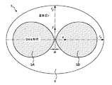
図1Aの平面図及び図1Bの断面図にて示すように、パッチアンテナ1は、金属グランドプレーン2と、吸収体層3と、誘電体基板4と、グランドプレーン2とは反対側の基板4の(上)面に付着された二つのパッチ5a、5bとの積層体を含む。パッチ5aと5bの各々は、基板4及び吸収体層3を通って引き込まれた給電線6a又は6bに接続される。グランドプレーン2に設けられた中心孔は、給電線6aと6bをグランドプレーン2から分離する。グランドプレーン2と誘電体基板4との間に吸収材料からなる薄い吸収体層3を挿入することにより、抵抗装荷アンテナ設計の場合に通例発生していたように、アンテナ1の効率を大きく低下することなく、フローティンググランドプレーン2からの波反射を緩和するため、送信パルスのリンギング効果が軽減する。吸収体層3は、磁性体装荷吸収体ECCOSORB SF−1からなる。電磁波は損失の多い土壌を通って伝播するため、GPRシステムにおいて効率は重要な要素である。
As shown in the plan view of FIG. 1A and the cross-sectional view of FIG. 1B, the
パッチ5aと5bは、同一形状を有し、対称的に配置された超形状の羽であり、その輪郭プロファイルは、請求項1に記載の超形状公式の三つの連続パラメータによって決まる。
基板4は、アンテナ1に構造的剛性、開口空洞における磁場の閉じ込め、反射波の吸収をもたらし、また、構造の高さの低減を可能にする。基板4は、誘電率er=2.55を有する誘電体材料PREPERMからなる。
The
給電線6aと6bは、グランドプレーン2の円形スロットを通る100オームの入力インピーダンスを備える二つのめっきスルーホール(PTH)ピンによって形成される。実用的なPTH技術は、給電ピン6a、6bのリアクタンスを低減するため、及び帯域幅強化のために導入される。
Feed lines 6a and 6b are formed by two plated through-hole (PTH) pins with a 100 ohm input impedance through the circular slot of
超形状化ダイポールアンテナ1のリターンロスパラメータを図2に示す。アンテナ1は、低周波数スペクトル及び高周波数スペクトルにおける動作をもたらす0.5GHzから4.5GHzを上回る範囲に及ぶ周波数インピーダンス帯域幅を有することが分かる。アンテナ1がそのパッチ構造により占有する体積が小さいにもかかわらず、アンテナ1は、等価の大型アンテナの全スペクトル特性を保持していることに注目すべきである。アンテナ1は、差異のある給電線に適合するように約100オームの入力インピーダンスを示すように設計された。動作周波数範囲に渡る入力インピーダンスプロファイルを図3に示す。
Return loss parameters of the
タイムドメインアンテナ応答は、二つの部分、即ち、主パルス及びリンギング領域によって構成される。主パルスは、給電点における励起パルスの直接的な放射に起因するが、リンギング部分は、グランドプレーンからの不連続性及び反射によるアンテナ1の内部構造における電流パルスの反射によって生じる。過渡アンテナの主な目的は、ターゲットのマスキングを避けるためのパルスリンギング領域の低減である。アンテナ形状は、表面電流分布を決定するため、内部波反射に対して重要な役割を果たす。前記超形状公式は、三つのパラメータの調整を通してアンテナ形状を最適化する可能性を提供する。このようにして、望ましくない反射を引き起こすアンテナ構造におけるインピーダンス不連続性は、緩和することが出来る。
The time domain antenna response is composed of two parts: the main pulse and the ringing region. The main pulse is due to the direct emission of the excitation pulse at the feed point, but the ringing part is caused by the reflection of the current pulse in the internal structure of the
励起信号は、約0.6nsの幅を有するガウスパルスである。励起パルスの波形及びスペクトルを図4に示す。アンテナは電子微分回路として動作するため、出力波形は、理想的には、入力信号の時間微分であることが期待される。図5は、吸収層を有する場合と吸収層を有しない場合の側面方向に25cmの距離における送信パルスを示し、図6は、送信パルスのスペクトル成分を描写している。吸収体がない場合、中間構造体は、厚みh=47.08mmの誘電体材料PREPERMのみの基板4のみから構成されることになる。パルス振幅が吸収層により僅かな劣化しか示さない一方でリンギングが大幅に低減していることが分かる。具体的には、送信パルスのピークトゥピーク振幅は、抵抗装荷のある場合及び抵抗装荷のない場合の超形状のアンテナ1に関して、夫々、21.11V/m及び19.15V/mである。これは、吸収体の導入によるパルス振幅減少が約9%であることを意味する。
The excitation signal is a Gaussian pulse having a width of about 0.6 ns. The waveform and spectrum of the excitation pulse are shown in FIG. Since the antenna operates as an electronic differentiation circuit, the output waveform is expected to be ideally a time derivative of the input signal. FIG. 5 shows the transmission pulse at a distance of 25 cm in the lateral direction with and without the absorption layer, and FIG. 6 depicts the spectral components of the transmission pulse. When there is no absorber, the intermediate structure is composed only of the
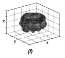
GPRアンテナに対する基本的な要求事項は、GPRシステムの電子機器に干渉しないように地面に向かって放射することである。また、上半分の空間からGPR受信アンテナへの外部信号の影響は最低限にしなければならない。従って、典型的には全方向に放射するダイポール状アンテナに関しては、遮蔽が必要である。遮蔽設計は、遮蔽がタイムドメインパルスに歪みを引き起こすため、難しい処理になる可能性がある。本発明に係るアンテナ1は、フローティンググランドプレーンのため、遮蔽機構を採用しなくても、上半分の空間からの電磁的分離をもたらす。このようにして、製造コストは大幅に減少されることが出来る。0.5GHz乃至4GHzの四つの異なる周波数における三次元の自由空間の放射パターンを図7に示す。特に、超形状のダイポールアンテナ1の正規化された放射パターンを、0.5GHz(図7A)、1GHz(図7B)、2GHz(図7C)、3GHz(図7D)、3.5GHz(図7E)、及び4GHz(図7F)にて示す。図から分かるように、アンテナ1は側面方向に向かって放射し、パターンは、動作周波数範囲に渡って比較的安定している。放射パターンの安定性及び限定的な圧縮及び歪みは、アンテナ1の短くなった長さ(典型的な既知のダイポールと比較して)及び全アンテナ領域に渡る電流の分布によるものである。
The basic requirement for a GPR antenna is to radiate towards the ground so as not to interfere with the electronics of the GPR system. Also, the influence of external signals from the upper half space to the GPR receiving antenna must be minimized. Thus, shielding is typically required for dipole antennas that typically radiate in all directions. Shielding designs can be a difficult process because shielding causes distortion in the time domain pulses. Since the
従って、図1A及び図1Bには、且つ図2から図7によって裏付けられるように、新規のコンパクトなアンテナが、GPR用途の単純なトポロジー及び固有のアーキテクチャと共に示されている。このアンテナは、前記超形状公式によって数学的に設計された第一の球根型GPRアンテナであり、様々な利点をもたらす。このアンテナは、0.5から4GHzの周波数範囲をカバーすることが出来、このようにして、探査深度と距離分解能の能力を同時にもたらすことが出来る。吸収層3の挿入により、アンテナ1の放射効率に大きく影響を及ぼすことなく後期リンギングが低減される。更に、アンテナ1は、既知のダイポール状設計とは対照的に、単一指向性放射を特徴とするため、遮蔽又は吸収空洞を必要としない。これにより、アンテナ1は、GPRシステムの低コストな解決法となる。また、アンテナ1は、大抵の従来のGPRアンテナと比べて、製造が容易で、ポータブルであり、且つ優れた性能を有する。
Thus, in FIGS. 1A and 1B, and as supported by FIGS. 2-7, a new compact antenna is shown with a simple topology and unique architecture for GPR applications. This antenna is the first bulb-type GPR antenna that is mathematically designed by the hyperform formula, and provides various advantages. This antenna can cover a frequency range of 0.5 to 4 GHz, thus providing the capability of exploration depth and distance resolution simultaneously. By inserting the
(その他の例)
図8を参照するが、図8は、米国特許第7,620,527号にも図16として組み込まれているが、本発明に係るアンテナのグランドプレーン及び/又はパッチの形状又は波形は、次の例示的な基本ステップの適用によって「合成」されることが出来る。
1)第一のステップでは、パラメータの選択が行われる(例えば、値をコンピュータ10に入力することによって、即ち、キーボード20、タッチスクリーン、マウスポインタ、音声認識装置、又はその他の入力装置等を介して、又は、コンピュータ10に値を指定させることによって)、コンピュータ10を使用して、パラメータの選択に基づいて選択された超形状を合成する。
2)第二の任意選択的なステップでは、超公式を使用して、選択した形状を適応させること、最適化を計算すること等が出来る。このステップは、グラフィックスプログラム(例えば、2D、3D等)、CADソフトウェア、有限要素解析プログラム、波生成プログラム、又はその他のソフトウェアの使用を含むことが出来る。
3)第三のステップでは、第一の又は第二のステップからの出力を使用して、例えば、(a)超形状31をモニタ30に表示し、超形状51をプリンタ50(2D又は3D)からの紙等の素材52に印刷することによって、(b)コンピュータ支援製造を行うことによって(例えば、ステップスリーの出力に基づいて、例えば、機械、ロボット等の外部デバイス60を制御することによって)、(c)スピーカシステム70等を介して音声71を生成することによって、(d)ステレオリソグラフィを行うことによって、(e)一般的には3D印刷技術に基づいてラピッドプロトタイピングを行うことによって、及び/又は(f)かかる形状を変形するための当該技術おいて既知の別の方法で出力を利用することによって、コンピュータ化された超形状を物理的な形態に変形する。
(Other examples)
Referring to FIG. 8, FIG. 8 is also incorporated as FIG. 16 in US Pat. No. 7,620,527. The shape or waveform of the ground plane and / or patch of the antenna according to the present invention is as follows. Can be “synthesized” by applying the following exemplary basic steps:
1) In the first step, a parameter is selected (for example, by inputting a value into the
2) In the second optional step, the hyperform can be used to adapt the selected shape, calculate the optimization, etc. This step can include the use of a graphics program (eg, 2D, 3D, etc.), CAD software, a finite element analysis program, a wave generation program, or other software.
3) In the third step, using the output from the first or second step, for example, (a) the
様々なコンピュータ支援製造(「CAM」)技術及びその技術から作製される製品は、当該技術では既知であり、任意の適切なCAM技術及び作製された製品が選択されることが出来る。CAM技術及びそれらの技術から作製される製品のごく一部の例として、次の米国特許(括弧内はタイトル)を参照することとし、それら特許の全開示は、参照によって本明細書に援用されるものとする。米国特許第5,796,986号(Method and apparatus for linking computer aided design databases with numerical control machine database)、米国特許第4,864,520号(Shape generating/creating system for computer aided design, computer aided manufacturing,computer aided engineering and computer applied technology)、米国特許第5,587,912号(Computer aided processing of three dimensional objects and apparatus therefor)、米国特許第5,880,962号(Computer aided processing of 3−D objects and apparatus thereof)、米国特許第5,159,512号(Cоnstruction of Minkowski sums and derivatives morphological combinations of arbitrary polyhedral in CAD/CAM systems)。 Various computer-aided manufacturing (“CAM”) technologies and products made from those technologies are known in the art, and any suitable CAM technology and manufactured product can be selected. For a few examples of CAM technology and products made from those technologies, reference is made to the following US patents (titled in parentheses), the entire disclosures of which are incorporated herein by reference: Shall be. US Pat. No. 5,796,986 (Method and apparatus for linking computer aided design databases with numerical control machine database), US Pat. No. 4,864,520 (Shape generating / creating system for computer aided design, computer aided manufacturing, computer aided engineering and computer applied technology), US Pat. No. 5,587,912 (Computer aided processing of three dimensions). onal objects and apparatus therefor), U.S. Pat. No. 5,880,962 (Computer aided processing of 3-D objects and apparatus thereof), U.S. Patent No. 5,159,512 (Cоnstruction of Minkowski sums and derivatives morphological combinations of arbitrary polyhedral in CAD / CAM systems).
様々なステレオリソグラフィ技術及びそれらの技術から作製される製品は、当該技術において既知であり、任意の適切なステレオリソグラフィ技術及び作製される製品が選択されることが出来る。ステレオリソグラフィ技術及びそれらの技術から作製される製品のごく一部の例としては、次の米国特許(括弧内はタイトル)を参照することとし、それら特許の全開示は、参照によって本明細書に援用されるものとする。米国特許第5,728,345号(Method for making an electrode for electrical discharge machining by use of a stereo lithography model)、米国特許第5,711,911号(Method of and apparatus for making a three−dimensional object by stereo lithography)、米国特許第5,639,413号(Methods and compositions related to stereo lithography)、米国特許第5,616,293号(Rapid making of a prototype part or mold using stereo lithography model)、米国特許第5,609,813号(Method of making a three−dimensional object by stereo lithography)、米国特許第5,609,812号(Method of making a three−dimensional object by stereo lithography)、米国特許第5,296,335号(Method for manufacturing fibre−reinforced parts utilizing stereo lithography tooling)、米国特許第5,256,340号(Method of making a three−dimensional object by stereo lithography)、米国特許第5,247,180号(Stereo lithographic apparatus and method of use)、米国特許第5,236,637号(Method of and apparatus for production of three dimensional objects by stereo lithography)、米国特許第5,217,653号(Method and apparatus for producing a stepless 3−dimensional object by stereo lithography),米国特許第5,184,307号(Method and apparatus for production of high resolution three−dimensional objects by stereo lithography)、米国特許第5,182,715号(Rapid and accurate production of stereo lithographic parts)、米国特許第5,182,056号(Stereo lithography method and apparatus employing various penetration depths)、米国特許第5,182,055号(Method of making a three−dimensional object by stereo lithography)、米国特許第5,167,882号(Stereo lithography method)、米国特許第5,143,663号(Stereo lithography method and apparatus)、米国特許第5,130,064号(Method of making a three dimensional object by stereo lithography)、米国特許第5,059,021号(Apparatus and method for correcting for drift in production of objects by stereo lithography)、米国特許第4,942,001号(Method of forming a three−dimensional object by stereo lithography and composition therefore)、米国特許第4,844,144号(Investment casting utilizing patterns produced by stereo lithography)。
Various stereolithography techniques and products made from those techniques are known in the art, and any suitable stereolithography technique and product made can be selected. For a few examples of stereolithography techniques and products made from those techniques, reference is made to the following US patents (titles in parentheses), the entire disclosure of which is hereby incorporated by reference: Shall be incorporated. U.S. Patent No. 5,728,345 (Method for making an electrical for electrical discharge by use of the stereolithology model, U.S. Patent No. 5,711,911) stereolithography), U.S. Pat. No. 5,639,413 (Methods and compositions related to stereolithography), U.S. Pat. No. 5,616,293 (Rapid making of a prototype type). ld using stereolithography model), U.S. Pat. No. 5,609,813 (Method of making a three-dimensional object of the stereolithology), U.S. Pat.No. 5,609,812 Lithography), U.S. Pat. No. 5,296,335 (Method for manufacturing fibre-reinforced parts utility stereolithography, U.S. Pat. No. 5,256,340) Dimensional object by stereolithography, United States Patent No. 5,247,180 (Stereolithographic and biofunctions and method of use), United States Patent No. 5,236,637 (Method of use and caps and methods). U.S. Pat. No. 5,217,653 (Method and apparatus for producing a stepless 3-dimensional object by stereolithography), U.S. Pat. No. 5,184,307 (Method a nd apparatus for production of high resolution three-dimensional objects by stereo lithography), US Pat. No. 5,182,715 (Rapid and accurate production of stereo lithographic parts), US Pat. No. 5,182,056 (Stereo lithography method and apparatus developing variant penetration depths), US Pat. No. 5,182,055 (Method of making a three-dimensional object by stereolithograph) hy), U.S. Pat. No. 5,167,882 (Stereo lithography method), U.S. Pat. No. 5,143,663 (Stereo lithography method and apparatus), U.S. Pat. No. 5,130,064 (Method of making). dimensional object by stereolithography), U.S. Pat.No. 5,059,021 (Apparatus and method for correcting for the production of
更に、本発明は、既知のマイクロステレオリソグラフィ手順で使用されることが出来る。従って、例えば、本発明は、コンピュータチップ及びその他の物品の作製において使用されることが出来る。一部の例示的な論文は次の通りであり、それらの開示は参照によって本明細書に援用されるものとする。A.Bertsch, H Lorenz, P.Renaud“3D microfabrication by combining microstereolithography and thick resist UV lithography”,Sensors and Actuators:A,73,pp.14−23,(1999).L.Beluze,A.Bertsch,P.Renaud“Microstereolithography:a new process to build complex 3D objects”,Symposium on Design,Test and microfabrication of MEMs/MOEMs,Proceedings of SPIE,3680(2),pp.808−817,(1999).A.Bertsch,H.Lorenz,P.Renaud“Combining Microstereolithography and thick resist UV lithography for 3D microfabrication”,Proceedings of the IEEE MEMS 98 Workshop,Heidelberg,Germany,pp.18−23,(1998).A.Bertsch,J.Y.Jezequel,J.C.Andre“Study of the spatial resolution of a new 3D microfabrication process:the microstereophotolithography using a dynamic mask−generator technique”,Journal of Photochem.and Photobiol.A:Chemistry,107,pp.275−281,(1997).A.Bertsch,S.Zissi,J.Y.Jezequel,S.Corbel,J.C.Andre,“Microstereophotolithography using a liquid crystal display as dynamic mask−generator”,Micro.Tech.,3(2),pp.42−47,(1997).A.Bertsch,S.Zissi,M.Calin,S.Ballandras,A.Bourjault,D.Hauden,J.C.Andre,“Conception and realization of miniaturized actuators fabricated by Microstereophotolithography and actuated by Shape Memory Alloys”,Proceedings of the 3rd France−Japan Congress and 1st Europe−Asia Congress on Mechatronics,Besancon,2,pp.631−634,(1996). Furthermore, the present invention can be used in known microstereolithographic procedures. Thus, for example, the present invention can be used in the manufacture of computer chips and other articles. Some exemplary papers are as follows, the disclosures of which are incorporated herein by reference. A. Bertsch, H Lorenz, P.M. Renaud, “3D microfabrication by combining microstereolithography and thick resist UV lithography”, Sensors and Actuators: A, 73, pp. 196 14-23, (1999). L. Belize, A.D. Bertsch, P.M. Renaud “Microstereolithography: a new process to build complex 3D objects”, Symposium on Design, Test and microfabrication of MEMs / MOEMs, ProSingp. 808-817, (1999). A. Bertsch, H.C. Lorenz, P.M. Renaud “Combining Microstereolithography and thick resist UV lithography for 3D microfabrication”, Proceedings of the IEEE MEMS 98 Working Hope, Hep. 18-23, (1998). A. Bertsch, J .; Y. Jezequel, J. et al. C. Andre “Study of the spatial resolution of a new 3D microfabrication process, the microstereomorphic using the dynamic masker. and Photobiol. A: Chemistry, 107, pp. 275-281, (1997). A. Bertsch, S.M. Zissi, J. et al. Y. Jezequel, S .; Corbel, J .; C. Andre, “Microstereophotolithography using a liquid crystal display as dynamic mask-generator”, Micro. Tech. , 3 (2), pp. 42-47, (1997). A. Bertsch, S.M. Zissi, M .; Calin, S.M. Ballandras, A.M. Bourjault, D.M. Hauden, J. et al. C. Andre, "Conception and realization of miniaturized actuators fabricated by Microstereophotolithography and actuated by Shape Memory Alloys", Proceedings of the 3rd France-Japan Congress and 1st Europe-Asia Congress on Mechatronics, Besancon, 2, pp. 631-634, (1996).
同様に、様々なラピッドプロトタイピング技術及びそれらの技術から作製される製品(例えば、成形品)が当該技術において知られており、任意の適切な技術及び作製される製品が選択されることが出来る。例えば、現在利用可能な三つの例示的な3Dモデルのラピッドプロトタイピング法として、その全開示が参照によって本明細書に援用されることとする米国特許第5,578,227号に開示されているように、a)光硬化液体凝固又はステレオリソグラフィ(例えば、上記を参照)、b)選択的レーザ焼結法(SLS)又は粉末層焼結法、c)熱溶解積層法(FDM)又は押出溶融プラスチック積層法が挙げられる。ラピッドプロトタイピング技術及びそれら技術から作製される製品のごく一部の例としては、次の米国特許(括弧内はタイトル)を参照することとし、それら特許の全開示は参照によって本明細書に援用されるものとする。米国特許第5,846,370号(Rapid prototyping process and apparatus therefor)、米国特許第5,818,718号(Higher order construction algorithm method for rapid prototyping)、米国特許第5,796,620号(Computerized system for lost foam casting process using rapid tooling set−up)、米国特許第5,663,883号(Rapid prototyping method)、米国特許第5,622,577号(Rapid prototyping process and cooling chamber therefor)、米国特許第5,587,913号(Method employing sequential two−dimensional geometry for producing shells for fabrication by a rapid prototyping system)、米国特許第5,578,227号(Rpid prototyping system)、米国特許第5,547,305号(Rapid,tool−less adjusting system for hot stick tooling)、米国特許第5,491,643号(Method for optimizing parameters characteristic of an object developed in a rapid prototyping system)、米国特許第5,458,825号(Utilization of blow molding tooling manufactured by stereo lithography for rapid container prototyping)、米国特許第5,398,193号(Method of three−dimensional rapid prototyping through controlled layerwise deposition/extraction and apparatus therefor)。
Similarly, various rapid prototyping techniques and products made from those techniques (eg, molded articles) are known in the art, and any suitable technique and product made can be selected. . For example, three exemplary 3D model rapid prototyping methods currently available are disclosed in US Pat. No. 5,578,227, the entire disclosure of which is hereby incorporated by reference. A) photocured liquid solidification or stereolithography (see above, for example), b) selective laser sintering (SLS) or powder layer sintering, c) hot melt lamination (FDM) or extrusion melting The plastic lamination method is mentioned. For a few examples of rapid prototyping techniques and products made from those techniques, reference is made to the following US patents (titles in parentheses), the entire disclosures of which are incorporated herein by reference: Shall be. U.S. Pat. No. 5,846,370 (Rapid prototyping process and apparatus thefore), U.S. Pat. No. 5,818,718 (Higher construction construction quat,
上述の三つのステップ、即ち段階は、図9に示す概略図でも概略的に説明される(ステップ1及び2は、図示のコンピュータ自体内で実行されることが出来る)。この図面は、米国特許第7,620,527号の図17に対応する。次のセクションでは、超公式によるパターン「合成」の幾つかの例示的実施形態が更に詳細に説明される。
The above three steps or stages are also schematically illustrated in the schematic diagram shown in FIG. 9 (
A.2Dグラフィカルソフトウェア
本発明は、2Dグラフィックソフトアプリケーションにおいて有用性が大きい。本発明は、例えば、Corel−Draw(商標)及びCorel−Paint(商標),Open Officeアプリケーション、 Adobe Illustrator and Photoshop(商標)のSupergraphx(商標),Adobe Photoshop(商標)等の従来の商用プログラムにおいて、Visual Basic(商標)又はWindows(商標)における様々な描画プログラムにおいて、又は、例えば、Lotus WordPro(商標)及びLotus Freelance Graphics(商標)、Java(商標)、Visual C(商標)、Visual C++(商標)及びあらゆるその他のC環境のようなその他の環境において適用されることが出来る。とりわけ、本アプローチは、古典的関数(累乗、三角関数等)を備える前記超公式のみを利用すればよいだけなので、コンピュータメモリ空間の相当な節約が可能なため、本発明は、画像合成において相当な利点を有する。更に、前記超公式によって利用可能な画像形状の数は、以前に利用可能な画像形状の数よりも相当増加する。グラフィックスプログラム(Windows(商標)のペイント、Microsoft Word(商標)の描画ツール、Corel−Draw(商標)、CAD、建築設計において使用されるもの等)は、コンピュータにプログラムされた形状である「プリミティブ」を使用する。これらは非常に限定的であり、例えば、多くの場合、主に円、楕円、正方形、及び矩形に限定される(3Dでは、体積プリミティブも非常に限定的である)。前記超公式の導入により、2Dグラフィックス(また以下に記述するように3Dグラフィックスにおいても)全体的な可能性が桁違いに大幅に拡大する。線形演算子として使用されるため、前記超公式は、極座標等であれ、また球座標、円柱座標、均質化した円柱のパラメトリック公式化等を使用する3Dでも、様々な方法及び公式で演算することが出来る。
A. 2D Graphical Software The present invention has great utility in 2D graphic software applications. The present invention includes conventional commercial programs such as Corel-Draw (TM) and Corel-Paint (TM), Open Office application, Supergraphx (TM), Adobe Photoshop (TM), Adobe's Illustrator and Photoshop (TM), etc. In various drawing programs in Visual Basic ™ or Windows ™ or, for example, Lotus WordPro ™ and Lotus Freegraphic Graphics ™, Java ™, Visual C ™, Visual C ++ ™ And can be applied in other environments, such as any other C environment. In particular, this approach only requires the use of the above-mentioned super formulas with classical functions (powers, trigonometric functions, etc.), so that considerable savings in computer memory space are possible, so the present invention is significant in image synthesis. Have the following advantages. Furthermore, the number of image shapes available by the super formula is considerably greater than the number of image shapes previously available. Graphics programs (such as Windows ™ paint, Microsoft Word ™ drawing tools, Corel-Draw ™, CAD, those used in architectural design, etc.) are computer-programmed shapes “primitives” Is used. These are very limited, for example, often limited primarily to circles, ellipses, squares, and rectangles (in 3D, volume primitives are also very limited). With the introduction of the super formula, the overall possibilities of 2D graphics (and also in 3D graphics as described below) are greatly expanded by orders of magnitude. Since it is used as a linear operator, the super-formula can be computed in various ways and formulas, such as polar coordinates, or 3D using spherical coordinates, cylindrical coordinates, parametric formulation of a homogenized cylinder, etc. I can do it.
2Dグラフィックソフトウェアアプリケーションの範囲内における一部の例示的な実施形態は次の通りである。
a.1.コンピュータは、例えば、極座標において又はXY座標において、ごく普通にオペレータを利用するように構成される。この意味で、パラメータは、(例えば、オペレータ入力によって又はコンピュータ自体によって)選択され、前記超公式において(例えば、プログラミングによって)入力として使用されることが出来る。個別の形状又は物体は、物体を印刷したり表示したりする等、任意の方法で使用されることが出来る。
a.2.コンピュータは、面積、周囲長、慣性モーメント等を計算するために積分等の演算を行うように構成されることも出来る。この点に関して、コンピュータは、a)オペレータ入力によって(例えば、キーボード20を介して)かかる演算を選択することによって、又はb)かかる演算を行うように(例えば、プログラミングを介して)コンピュータの構成を行うことによって、かかる演算を行うように構成されることが出来る。
a.3.コンピュータは、a)形状を表示又は提示するように、b)ユーザがそれらの表示の後にかかる形状を修正することが出来るように、及びc)ユーザによって修正された形状を表示するように(例えば、ソフトウェアを介して)構成されることが出来る。この点について、ユーザは、例えば、パラメータを変更することによって形状を修正することが出来る。例示的な一実施形態では、コンピュータは、ステップスリーにおいて創造された物理的表現に物理的に作用することによって表示される或いは提示される(即ち、上述のステップスリーにて提示される)形状を可能にするように構成されることが出来る。好適な一実施形態では、コンピュータは、モニタに表示された形状が、パターン、例えば、画像の辺及び/又は角を引き出すことによって修正されることが出来るように構成されることが出来る。この点に関して、好ましくは、画像31は、コンピュータスクリーン又はモニタ30に表示され、ユーザは、自身の手で操作される「マウス」40(又はその他のユーザ操作スクリーン又はディスプレイポインタデバイス)を使用して、表示されたポインタ32を形状の上に載置し、ポインタ32を「クリック」して新しい位置33に「ドラッグ」することによって、新たな「超形状」の構成34を呈するように超形状を修正することが出来る。これは、公式及びパラメータの再計算も含むことになるだろう。
a.4.コンピュータは、a1又はa3にて生成された個別の形状の二つ以上を、重畳処理のいずれかを通して、互いに融合するブール演算を行うように構成されることも出来る。場合によっては、例えば、重畳及び/又は反復等によって組み合わせられた個別の超形状は、例えば、異なる断面又は領域を有する形状を作成するために組み合わせ可能な扇形又は断面でもよい(単に一例として、例えば、0からπ/2の間の円の扇形は、例えば、π/2からπの間の正方形の扇形と組み合わされて複数の構成要素からなる形状を創出することが出来る)。コンピュータは、作成された超形状に更なる演算を行うように、例えば、かかる形状を平坦化、スキュー、伸長、拡大、回転、移動又は並進、又はその他の方法で修正するように構成されることも出来る。
Some exemplary embodiments within the scope of 2D graphics software applications are as follows.
a. 1. The computer is configured to utilize the operator quite commonly, for example in polar coordinates or in XY coordinates. In this sense, parameters can be selected (eg, by operator input or by the computer itself) and used as input in the paraform (eg, by programming). Individual shapes or objects can be used in any way, such as printing or displaying an object.
a. 2. The computer can also be configured to perform operations such as integration to calculate area, perimeter, moment of inertia, and the like. In this regard, the computer can configure the computer to: a) select such an operation by operator input (eg, via keyboard 20), or b) perform such an operation (eg, via programming). By doing so, it can be configured to perform such operations.
a. 3. The computer a) displays or presents the shapes, b) allows the user to modify such shapes after their display, and c) displays the shapes modified by the user (eg, , Via software). In this regard, the user can correct the shape by changing parameters, for example. In one exemplary embodiment, the computer displays the shape displayed or presented (ie, presented at the above step three) by physically acting on the physical representation created at the step three. Can be configured to enable. In a preferred embodiment, the computer can be configured such that the shape displayed on the monitor can be modified by extracting patterns, eg, edges and / or corners of the image. In this regard, preferably, the
a. 4). The computer can also be configured to perform a Boolean operation that fuses two or more of the individual shapes generated in a1 or a3 with each other through either superposition processing. In some cases, the individual super-shapes combined, eg, by overlapping and / or repeating, etc. may be, for example, sectors or cross-sections that can be combined to create shapes having different cross-sections or regions (for example, as an example only) , A circular sector between 0 and π / 2 can be combined, for example, with a square sector between π / 2 and π to create a shape consisting of multiple components). The computer is configured to perform further operations on the created supershape, for example, to flatten, skew, stretch, enlarge, rotate, move or translate, or otherwise modify such shape You can also.
B.3Dグラフィカルソフトウェア
2Dアプリケーションと同様に、本発明は、3Dグラフィックアプリケーションにおいて(及び様々なその他の次元における表現において)有用性が大きい。
本発明は、例えば、コンピュータ支援設計(「CAM」)ソフトウェア、有限要素解析(「FEM」)用ソフトウェア、Supergraphx 3D Shape Explorer、CST、Ansoft HFSS、Remcom XFdtd、EMSS Feko、Empire XCcel等のアンテナ設計及び解析ソフトウェア、建築設計ソフトウェア等において適用可能である。本発明により、例えば、様々な用途に向けて、スプライン関数ではなく単一連続関数を使用することが出来るようになる。CADの産業的用途としては、例えば、ラピッドプロトタイピング、又は3D印刷を含むコンピュータ支援製造(「CAM」)における使用を含む。
B. 3D Graphical Software Like 2D applications, the present invention has great utility in 3D graphic applications (and in representations in various other dimensions).
The present invention includes, for example, computer-aided design ("CAM") software, finite element analysis ("FEM") software, Supergraphx 3D Shape Explorer, CST, Anft HFSS, Remcom XFdtd, EMSS Feko, Empire XCcel, etc. It can be applied to analysis software, architectural design software, etc. The present invention makes it possible to use a single continuous function instead of a spline function, for example, for various applications. CAD industrial applications include, for example, rapid prototyping, or use in computer-aided manufacturing (“CAM”), including 3D printing.
本発明の好適な実施形態に係るパッチアンテナ300の一実施形態を示す図10A及び10Bを参照する。アンテナ300は、キャリア構造体として機能する基板301を含み、基板301は、基板301の一方の側の導電性グランドプレーン302と反対側に積層された複数の導電性パッチ303a、303b、304a、及び304bとを離間する。パッチ303a、303b、304a、及び304bは、二つのパッチ組になって配置され、各パッチ組は、一次パッチ303a、304aと、一次パッチ303a、304aに近い距離に配置された二次パッチ303b、304bとによって形成され、動作時に一次パッチ303a、304aと二次パッチ303b、304bの間で電磁相互作用が生じることが出来るようになっている。各一次パッチ303a、304aは、基板301から及びグランドプレーン302に設けられた中心孔から導出された給電プローブの、給電線、給電構造とも呼ばれる給電コネクタ305a、305bに接続される。二次パッチ303bと304bは、給電コネクタに直接的には接続されない。一次パッチ303aと304aの各々が給電コネクタ305a、305bに接続されているため、これらの一次パッチ303aと304aが最初に作動する。一次パッチ303aと304aの作動により、二次パッチ303bと304bが続いて作動(共振)することになる。各パッチ組(303a、303b、304a、304b)のベースプロファイルは、実質的に、次の極関数によって定義されるベースプロファイルに合致する。
この例では、次の値を使用して図10A及び図10Bに示すパッチ302(の断面)形状にする。即ち、a=b=5.74、m=1、及びn1=0.4825、およびn2=n3=1.0662。パッチ303a、303b、304a、及び304bの厚みは、典型的には約数マイクロメートルである。この例では、パッチ厚みtは、0.068mmに等しい。給電コネクタ305aと305bの間の距離wは、この例では5.253mmに等しい。各給電コネクタ305a、305bの直径即ち厚みdfは、この例では1.82に等しい。 In this example, the following values are used to form the patch 302 (cross section) shown in FIGS. 10A and 10B. That is, a = b = 5.74, m = 1, and n 1 = 0.4825, and n 2 = n 3 = 1.0662. The thickness of the patches 303a, 303b, 304a, and 304b is typically about a few micrometers. In this example, the patch thickness t is equal to 0.068 mm. The distance w between the power supply connectors 305a and 305b is equal to 5.253 mm in this example. Each power supply connector 305a, diameter or thickness d f of 305b in this example equal to 1.82.
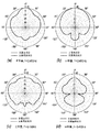
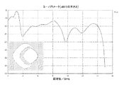
図10A及び図10Bに示すアンテナ300は、無指向性Wi−Fiデュアルバンドアンテナ300として構成され、2.2〜2.77GHz(802.11b/g/n)の第一の周波数帯域と4.53〜6.96GHz(802.11a/n/ac)の第二の周波数帯域の両方において動作するように構成される。両方の周波数帯域は、別々に制御されることが出来る。二次パッチ303bと304bは、アンテナ300がより低い周波数帯域で動作することを可能にするために重要な役割を果たす。各一次パッチ303a、304aと各二次パッチ303b、304bの間に配置されたギャップ306a、306bも同様である。ギャップ306a、306b(即ちスロット)のジオメトリは、上記の極関数によって定義される超形状のベースプロファイルの少なくとも一部に適合する。R関数を使用して、超形状のパッチ組と超形状のギャップ306a、306bの両方を組み合わせて超形状のジオメトリの組立体とすることが出来る。この例では、各ギャップ306a、306bは、円の弧の形を有する。周波数応答は、ギャップ幅によって決まることが実験により示されており、これを図11に示す。この例では、アンテナ300が両方の周波数帯域において非常に良好に動作する最適なギャップ幅は5ミリメートルである。その他のギャップ幅(より大きい又はより小さい)では、アンテナの性能が悪化することになる。この例では、基板301及びグランドプレーン302のx半径は8.64cmに等しく、y半径は5.92cmに等しい。基板301の厚みは、この例では9.525mmに等しく、これは、低い帯域における1/8波長に実質的に等しい。E平面とH平面の両方におけるアンテナ300の放射パターンを、2.45GHzの周波数と5.45GHzの周波数の両方において図12に示す。図面から分かるように、放射パターンは無指向性である。従って、バックキャビティは省略することが出来る。放射効率は非常に高く、98.5%から99.1%である。二つの対称平面の間では交差偏波が発生しない。従って、図10A及び図10Bに示すアンテナを使用することによって、優れたアンテナ性能が達成される。
An
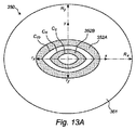
本発明に係る別のパッチアンテナ350を図13A(平面図)及び図13B(断面図)に示す。アンテナ350は、アンテナ350のコアを形成する誘電基板351を含む。基板351の上面は、二つの金属パッチ352aと352b、特に、内側パッチ352a(一次パッチ)と、内側パッチ253aを包囲する外側パッチ352b(二次パッチ)とを備える。基板351の底面は、金属グランドプレーン353を備える。グランドプレーン353は、内側パッチ253aに接続された金属給電コネクタ354のための貫通開口を包囲する管状の中心部353aを備える。この目的のため、給電コネクタ354は、誘電基板351を通って延在している。パッチ352aと352bと、一方の側の給電コネクタ354と、他方の側のグランドプレーン353とは、互いに分離(絶縁)されている。パッチ352aと352bの組立体、特にこの組立体のジオメトリは、請求項1に記載の極関数によって定義される超形状に基づくベースプロファイルの重畳に基づく。より具体的には、図示の組立体は、四つの重畳層からなり、連続的に、楕円形の中実な(材料で充填された)外形によって第一層が形成され、超形状の、特に口形状の中空な(材料のない)層によって第二層が形成され、より小さな超形状の、特に口形状の中実層によって第三層が形成され、より小さな重畳された、特に口形状の中空層によって、重畳された最上層(第四層)が形成される。この層の重畳により、図示のように、一次パッチ352aは、内縁C1iと外縁C1oの両方において実質的に口形状になり、一次パッチ352Aは、二次パッチ352bによって包囲され、二次パッチ352bの内縁C2iは実質的に口形状になり、二次パッチ352bの外縁は楕円形に形成される。コンピュータデバイスにより、超形状の層の前記重畳は、R関数を用いることによって容易に行うことが出来る。縁が夫々C1i、C1o、及びC2iに対応するベースプロファイルをもたらす極関数において、次のパラメータが使用される。
Another
実験的な試験によれば、上記値は、2.4GHz(2.35〜2.52GHz)及び5GHz(5.12GHz〜5.94GHz)周波数帯域におけるWi−Fiデュアルバンドアンテナとしてのアンテナ350の最高の性能を得るために、パッチ352a、352b及び前記パッチ352a、352b間に配置されたギャップ355の最適な設計をもたらしている。誘電体基板351及びグランドプレーン353は、同一の楕円形の設計及び寸法を有する。基板351及びグランドプレーン353の長さRxは、この例では、39.7mmに等しく、幅Ryは、33.7mmに等しい。この例における二次パッチ352bの外側寸法は、長さrxが19.8mmに等しく、幅ryが11.8mmに等しい。基板351の厚みhは、この例では、9.525mmに等しい。パッチ厚みtは0.07mmに等しい。給電コネクタ354の厚みdfは1.28mmに等しい。グランドプレーン353の管状部353aの内径Dfは4.28mmに等しい。これにより、給電コネクタ354とグランドプレーン353の間に1.5mmの距離がもたらされる。
According to experimental tests, the above values are the highest of the
図14に示すように、実現した放射パターンは一方向性である。放射効率は比較的高く、94.4%から98.8%まで変化する。実現した利得も優れた結果を示し、6.84dBと7.08dの間に位置している。 As shown in FIG. 14, the realized radiation pattern is unidirectional. The radiation efficiency is relatively high and varies from 94.4% to 98.8%. The realized gain also shows excellent results and is located between 6.84 dB and 7.08 d.
図15は、本発明の別の好適な一実施形態、即ち、パッチ402、給電コネクタ404、及び基板406を含むパッチアンテナ400の立体図を示す。基板の背面は、グランドプレーン(図15では見えない)によって覆われており、基板の表面は、グランドプレーンと同一の大きさである。グランドプレーンとパッチ402の厚みは、グランドプレーンに比べてかなり小さくなっている。基板406は、誘電体材料から作製され、グランドプレーンとパッチ402の間のスペーサ構造体として作用する。給電コネクタ404は、基板406の表面上に引き込まれたマイクロストリップの形状を有している。パッチ402のベースプロファイルは、実質的に、次の極関数によって定義されるベースプロファイルと略合致している。
この例では、次の値を使用して図示のパッチ406の形状にする。即ち、m1=4、m2=4、a=1、b=1、n1=2、n2=6、及びn3=6である。 In this example, the following values are used to shape the illustrated patch 406: That is, m 1 = 4, m 2 = 4, a = 1, b = 1, n 1 = 2, n 2 = 6, and n 3 = 6.
図15に示すパッチアンテナ400は、10.2GHzの周波数帯域にて動作するように構成された単一帯域アンテナとして構成されている。10.2GHzでのアンテナの全効率は、約82%である。最大指向性は13.2dBiである(比較:短いダイポールアンテナは1.76dBiを達成し、大型の皿型アンテナは50dBiを達成する)。
The
(比較例)
図16は、円形パッチ452、給電コネクタ454、及び基板456を含む先行技術に係るパッチアンテナ450の既知の設計の立体図を示す。基板の背面は、グランドプレーン(図16では見えない)によって覆われており、基板の表面は、グランドプレーンと同一の大きさである。グランドプレーンとパッチ452の厚みは、グランドプレーンに比べてかなり小さくなっている。
(Comparative example)
FIG. 16 shows a three dimensional view of a known design of a
基板456は、誘電体材料から作製され、グランドプレーンとパッチ452の間のスペーサ構造体として作用する。給電コネクタ454は、基板456の表面上に引き込まれたマイクロストリップの形状を有する。円形パッチ452のベースプロファイルは、ベースプロファイルを画定する極関数に関してm1=0且つm2=0であることを必要とするため、本発明に係るベースプロファイルと合致しない。図15に示すパッチアンテナ450は、11.12GHzの周波数帯域にて動作するように構成された単一帯域アンテナとして構成されている。11.12GHzでのアンテナの全効率は、約4.2%である。11.12GHzでの最大指向性は5.6dBiである。
The
この比較例は、パッチのベースプロファイルが請求項1で言及される超公式によって実質的に定義されるようにパッチのベースプロファイルを再設計することによって、既知のパッチアンテナの全効率及び最大指向性を大幅に上昇させることが出来ることを証明している。
This comparative example shows the overall efficiency and maximum directivity of a known patch antenna by redesigning the patch base profile so that the patch base profile is substantially defined by the super formula referred to in
図17は、本発明に係る別のパッチアンテナ500の断面図を示す。パッチアンテナ500は、導電性のグランドプレーン502を支持するため及び少なくとも一つの導電性パッチ503を支持するために取り付け構造体として作用する誘電体のU字形のスペーサ構造体501を含む。グランドプレーン502と少なくとも一つのパッチ503の間には誘電体の空隙504が存在する。少なくとも一つのパッチが給電コネクタ(図示せず)に接続される。給電コネクタとグランドプレーン502は両方とも、アンテナ500に電力を供給するための電源(図示せず)に接続される。パッチ503及び結果的にはグランドプレーン502のベースプロファイルは、次の極関数によって設計及び定義される。
上述のように、少なくとも一つの超形状のパッチの適用により、アンテナ性能の大幅な改善がもたらされる。 As mentioned above, the application of at least one super-shaped patch provides a significant improvement in antenna performance.
(超広帯域アンテナの例)
本発明に係る超形状のパッチアンテナは、アンテナが2から20GHzまでの周波数範囲に渡って動作可能でありながら、略全ての周波数範囲に渡って約−10dB又は−10dB未満の大きさでSパラメータを達成することが必要である超広帯域アンテナ(UWA)を設計するために使用されることも出来る。
(Example of ultra-wideband antenna)
The super-shaped patch antenna according to the present invention is capable of operating over the frequency range from 2 to 20 GHz, while the S parameter has a magnitude of less than about -10 dB or less than -10 dB over almost all frequency ranges. Can also be used to design ultra wideband antennas (UWA) that are required to achieve
連邦通信委員会(FCC)及び国際電気通信連合無線通信部門(ITU−R)は、現在、アンテナからの送信に関するUWBを、放射された信号の帯域幅が500MHz又は中心周波数の20%のいずれか小さい方を超過するものと定義している。 The Federal Communications Commission (FCC) and the International Telecommunication Union Radiocommunications Department (ITU-R) are currently using UWB for transmission from antennas, either with a radiated signal bandwidth of 500 MHz or 20% of the center frequency. It is defined as exceeding the smaller one.
円状の超形状
パッチアンテナは、次の基本的な組み立て、即ち、
導電性パッチ、
矩形の導電性グランドプレーン、
グランドプレーンから絶縁され、少なくとも一つのパッチに導電的に接続される50オームのインピーダンスの給電を行うマイクロストリップの形状の少なくとも一つの給電コネクタ、及び
前記少なくとも一つのパッチと前記少なくとも一つのグランドプレーンを分離するための少なくとも一つの誘電基板、
を有し、
実質的に超形状の少なくとも一つのベースプロファイルの少なくとも一部によって少なくとも一つのパッチが画定され、前記超形状のベースプロファイルは、極関数によって定義される。
Conductive patch,
Rectangular conductive ground plane,
At least one power supply connector in the form of a microstrip, which is insulated from the ground plane and electrically conductively connected to at least one patch, and which feeds power of 50 ohms, and the at least one patch and the at least one ground plane At least one dielectric substrate for separation,
Have
At least one patch is defined by at least a portion of the at least one substantially super-shaped base profile, the super-shaped base profile being defined by a polar function.
更に、超形状のパッチは、次の条件、即ち、
m1はm2に等しく、1から3.5までの範囲に及び、
a=b=1であり、
n3はn2に等しく、0.7から3までの範囲に及び、且つ
n1は0.5から3の範囲に及び、
且つ、より具体的には、
m1はm2に等しく、1から3.5までの範囲に及び、
a=b=1であり、
次のうち、
n3はn2に等しく、3、1、及び0.7から選択される一方でn1=3、
n3はn2に等しく、3、2.5、及び1から選択される一方でn1=1、
n3はn2に等しく且つ3である一方でn1=0.7、又は
n3はn2に等しく且つ2.5である一方でn1=0.5
のいずれかと組み合わされる条件を満足する。
Furthermore, the super-shaped patch has the following conditions:
m1 is equal to m2 and ranges from 1 to 3.5;
a = b = 1,
n3 is equal to n2, ranges from 0.7 to 3, and n1 ranges from 0.5 to 3.
And more specifically,
m1 is equal to m2 and ranges from 1 to 3.5;
a = b = 1,
Of the following
n3 is equal to n2 and is selected from 3, 1, and 0.7 while n1 = 3,
n3 is equal to n2 and is selected from 3, 2.5 and 1 while n1 = 1,
n3 is equal to n2 and 3 while n1 = 0.7, or n3 is equal to n2 and 2.5 while n1 = 0.5
Satisfy the conditions combined with any of the above.
図18a及び図18bは、上記で定義した円状の超形状のパッチアンテナの二つの例を、各々の広帯域特性のグラフと共に示す。
図18a及び図18bの挿入図には、次の条件、即ち
a)に関しては、m1=m2=2.25、n3=n2=2.7、a=b=1、n1=1.43、c=13.28、
b)に関しては、m1=m2=1.65、n3=n2=3.6、a=b=1、n1=0.65、c=12.14。
を満たす二つの超形状が描かれており、cは、ρd(j)に乗算する因子であるスケール因子である。
FIGS. 18a and 18b show two examples of circular super-shaped patch antennas as defined above, together with their respective broadband characteristic graphs.
In the insets of FIGS. 18a and 18b, for the following conditions: a), m 1 = m 2 = 2.25, n 3 = n 2 = 2.7, a = b = 1, n1 = 1 .43, c = 13.28,
For b), m 1 = m 2 = 1.65, n 3 = n 2 = 3.6, a = b = 1, n1 = 0.65, c = 12.14.
2 are drawn, and c is a scale factor that is a factor by which ρd (j) is multiplied.
これらのグラフは、両方の超形状のパッチアンテナが、2から20GHzまでの広い周波数範囲に渡って約−10dB又は−10dB未満のS11の大きさを達成することを示している。 These graphs show that both super-shaped patch antennas achieve a S11 magnitude of about -10 dB or less than -10 dB over a wide frequency range from 2 to 20 GHz.
従来の円形のモノポールと比較した場合のこの円形のパッチアンテナの一つの更なる利点は、より低い周波数でのインピーダンス整合特性が向上することにある。これは、大幅な向上であり、結果的に、アンテナ帯域幅も増大する。 One further advantage of this circular patch antenna when compared to a conventional circular monopole is improved impedance matching characteristics at lower frequencies. This is a significant improvement and, as a result, the antenna bandwidth also increases.
細長い楕円状の超形状
上述の円形状の超形状の特別な細長い変形は、上記と同一の基本的な組み立てに基づいて得られ、
m1=m2=1であり、
a=b=1であり、
n3はn2に等しく、1から10までの範囲に及び、
n1は1から1.5までの範囲に及ぶ
というパラメータの組み合わせを有する点で異なる。
これにより、20GHzと26GHzの範囲で変化する帯域幅を得ることが出来る。
Elongate elliptical super-shape The special elongate deformation of the above-mentioned circular super-shape is obtained based on the same basic assembly as above,
m1 = m2 = 1,
a = b = 1,
n3 is equal to n2 and ranges from 1 to 10;
n1 is different in that it has a combination of parameters ranging from 1 to 1.5.
Thereby, the bandwidth which changes in the range of 20 GHz and 26 GHz can be obtained.
正方形の超形状
正方形の超形状は、上記と同一の基本的な組み立てに基づいて得られ、
m1はm2に等しく、3.6から4.5までの範囲に及び、
a=b=1であり、
n3=n2=3であり、且つ、
n1=3である。
というパラメータの組み合わせを有する点で異なる。
Square super shape Square super shape is obtained based on the same basic assembly as above,
m1 is equal to m2 and ranges from 3.6 to 4.5;
a = b = 1,
n3 = n2 = 3 and
n1 = 3.
It is different in that it has a combination of parameters.
図19は、上記に定義した正方形の超形状のパッチアンテナ(右下)と、一般的に使用される正方形のパッチアンテナ(右上)の描画を、夫々の広帯域幅特性のグラフ(下側の線が超形状のパッチアンテナに対応)と共に示す。 FIG. 19 shows a plot of the above-defined square super-shaped patch antenna (lower right) and a commonly used square patch antenna (upper right). Corresponding to a super-shaped patch antenna).
当グラフは、正方形の超形状のパッチアンテナが、3から30GHzまでに及ぶ広い周波数範囲に渡って−10dB未満のS11に関する大きさを達成することを示している。対照的に、一般的な正方形のパッチアンテナは、そのような値、約2、17、及び25GHzのみを達成するが、全周波数範囲に及んでは達成しない。 The graph shows that the square super-shaped patch antenna achieves a magnitude for S11 of less than -10 dB over a wide frequency range ranging from 3 to 30 GHz. In contrast, a typical square patch antenna achieves only such values, approximately 2, 17, and 25 GHz, but not over the full frequency range.
更に、正方形の超形状のパッチアンテナは、一般的な正方形のパッチアンテナと比べて、2から30GHzまでに及ぶ全周波数範囲に渡ってより低い又は同様な入力反射係数を達成する。 Furthermore, a square super-shaped patch antenna achieves a lower or similar input reflection coefficient over the entire frequency range extending from 2 to 30 GHz compared to a typical square patch antenna.
スロット付き超形状(1)
スロット付き超形状は、上記に示す同一の組み立てに基づいて得られ、前記パッチが、パッチ内の切除領域であるスロットを備え、次の極関数によって定義され、
A slotted supershape is obtained based on the same assembly shown above, where the patch comprises a slot that is an ablation region in the patch and is defined by the following polar function:
図20は、上記に定義したスロット付き超形状のパッチアンテナの形状を挿入図にて、固有の広帯域特性を描く図と共に示す。
当グラフは、2から20GHzまでの周波数範囲に渡って十分な感度を示している。図21は、同一のスロット付き超形状のパッチアンテナの効率のグラフを示す。この効率は、同一の周波数範囲に渡って少なくとも90%以上である。
FIG. 20 shows the shape of a super-shaped patch antenna with a slot as defined above in an inset, together with a diagram depicting the inherent broadband characteristics.
The graph shows sufficient sensitivity over the frequency range from 2 to 20 GHz. FIG. 21 shows a graph of the efficiency of the same slotted super-shaped patch antenna. This efficiency is at least 90% over the same frequency range.
スロット付き超形状(2)
UWB用のその他のスロット付き超形状のパッチアンテナを考えることも出来る。
例えば、一次パッチ内のスロットの切除領域内に二次パッチが存在する設計が効果的になり得る。
かかるスロット付き超形状は、上記に示す同一の基本的な組み立てに基づいて得られ、前記パッチは、前記パッチ内の切除領域であるスロットを備え、
前記スロットが、二次パッチを備え、
一次パッチとも呼ばれる前記主パッチ、前記スロット、及び前記二次パッチは全て、極関数によって定義されるという点で異なる。
Other slotted super-shaped patch antennas for UWB can also be considered.
For example, a design in which a secondary patch exists in the ablation region of a slot in the primary patch can be effective.
Such a slotted super-shape is obtained based on the same basic assembly shown above, the patch comprising a slot that is an ablation region in the patch,
The slot comprises a secondary patch;
The main patch, also called the primary patch, the slot, and the secondary patch are all different in that they are defined by polar functions.
より概括的に言うならば、本発明は、c1、c2、及びc3の値がc1>c2>c3という条件を満たす限り上記値とは異なることが出来る上記のスロット付き超形状を含む。 More generally speaking, the present invention includes the above-described slotted supershape that can differ from the above values as long as the values of c1, c2, and c3 satisfy the condition of c1> c2> c3.
図22は、このような一次パッチ及び二次パッチを有するスロット付き超形状を、夫々の広帯域幅特性を強調するグラフと共に示す。
当グラフから、4から15GHzに渡り、S11の大きさは、必要に応じて、約−10dB又は−10dB未満であるということになる。
上記設計に係るUWBパッチアンテナは、給電構造がマイクロストリップ線であり、パッチの垂直な対称平面から距離を置いて前記対称平面に平行に配置され、前記距離が前記マイクロストリップの幅よりも大きい場合に、得られる帯域幅を更に向上し得る。
例えば、0.5から2.0mmまでのマイクロストリップラインを使用する場合、2.0と5.0mmの間の対称平面からの距離により、結果的に帯域幅を増大することが出来、その帯域幅は、使用されるパッチの具体的なベースプロファイルによっては、10GHz以上になり得る。
FIG. 22 shows such a slotted super-shape with primary and secondary patches, along with a graph highlighting the respective wide bandwidth characteristics.
From this graph, it can be seen that over 4 to 15 GHz, the magnitude of S11 is about -10 dB or less than -10 dB as required.
In the UWB patch antenna according to the above design, the feeding structure is a microstrip line, arranged parallel to the symmetry plane at a distance from the vertical symmetry plane of the patch, and the distance is larger than the width of the microstrip In addition, the obtained bandwidth can be further improved.
For example, when using microstrip lines from 0.5 to 2.0 mm, the distance from the plane of symmetry between 2.0 and 5.0 mm can result in an increase in bandwidth and the bandwidth The width can be 10 GHz or more depending on the specific base profile of the patch used.
(まとめ)
本発明は、本明細書にて図示及び説明された例示的実施形態に限定されないこと、添付の請求項の範囲内で、当業者に自明であろう数々の変形が可能であることは明らかになろう。更に、本開示に基づき、本発明は、数々の発明的装置、構成要素、態様、方法などを含む数々の実施形態を有することが理解される。本明細書では、「本発明(the invention)」との言及は、本発明の全ての実施形態に当てはまることを意図しない。
(Summary)
It will be apparent that the invention is not limited to the exemplary embodiments shown and described herein, and that many modifications will be apparent to those skilled in the art within the scope of the appended claims. Become. Further, based on this disclosure, it is understood that the present invention has numerous embodiments, including numerous inventive devices, components, aspects, methods and the like. In this specification, references to “the invention” are not intended to apply to all embodiments of the invention.
本概要は、本明細書の範囲内に開示される概念の概論を提供するものであり、多くの教示と、本開示の範囲内で拡大させた議論において提供されるこれら教示における変化を網羅したリストとなるものではない。従って、本概要の内容は、次の請求項の範囲を制限するものとして使用されるべきではない。 This summary provides an overview of the concepts disclosed within the scope of this specification and covers many teachings and variations in these teachings provided in an expanded discussion within the scope of this disclosure. Not a list. Accordingly, the content of this summary is not to be used as limiting the scope of the following claims.
発明の概念は、一連の例において説明され、二つ以上の発明の概念を示す例もある。個々の発明の概念は、特定の例において提供された全ての細部を実施しなくても実施されることが出来る。当業者は、様々な例にて説明された発明の概念が、特定の用途に対処するために互いに組み合わされることが出来ることを理解するので、以下に提供される発明の概念の全ての考え得る組み合わせの例を提供する必要はない。 The inventive concept is illustrated in a series of examples, with some examples showing more than one inventive concept. Individual inventive concepts may be practiced without the implementation of all the details provided in the specific examples. Those skilled in the art will understand that the inventive concepts described in the various examples can be combined with each other to address a particular application, so that all possible inventive concepts provided below are considered. There is no need to provide examples of combinations.
開示された教示のその他のシステム、方法、特徴、及び利点は、次の図面及び詳細な説明の考察により、当業者には明らかになるだろう。全てのこのような更なるシステム、方法、特徴、及び利点は、添付の請求項の範囲内に含まれ、それによって保護されることを意図している。 Other systems, methods, features, and advantages of the disclosed teachings will become apparent to those skilled in the art upon consideration of the following drawings and detailed description. All such further systems, methods, features, and advantages are intended to be included within the scope of the appended claims and protected thereby.
請求項における限定事項(例えば、後に追加されるものも含む)は、請求項にて採用された言語に基づいて広く解釈されるべきであり、本明細書にて又は出願手続きの遂行中に説明された例に限定されず、これらの例は、非排他的なものとみなされるべきである。例えば、本開示において、「好ましくは(preferably)」という言葉は非排他的であり、「に限定されないが、好ましくは(preferably, but not limited to)」を意味する。本開示において、及び本出願の手続きの遂行中において、ミーンズプラスファンクション又はステッププラスファンクション制限は、具体的な請求項の限定事項に関して、その限定事項において次の条件の全てが存在する場合にのみ採用されるだろう。即ち、a)「するための手段(means for)」又は「するためのステップ(step for)」が明示的に記載されている、b)対応する機能が明示的に記載されている、及びc)構造、材料、又はその構造を支持する作用が記載されていない。本開示において、及び本出願の手続きの遂行中において、「本発明(present invention)」又は「発明(invention)」という用語は、本開示の範囲内の一つ以上の態様を指すものとして使用される場合がある。本発明又は発明という言語は、臨界性を特定するものとして不適切に解釈されるべきではなく、全ての態様又は実施形態に渡って適用されるものと不適切に解釈されるべきではなく(即ち、本発明は、多くの態様又は実施形態を有するものと理解すべきである)、且つ本出願即ち請求項の範囲を制限するものと不適切に解釈されるべきではない。本開示において、及び本出願の手続きの遂行中において、「実施形態(embodiment)」という用語は、任意の態様、特徴、プロセス、又はステップ、それらの任意の組み合わせ、及び/又はそれらの任意の一部等を説明するために使用される場合がある。一部の例では、様々な実施形態が、重複する特徴を含む可能性がある。本開示において、「例えば(for example)」を意味する次の省略語“e.g.”が採用されている場合がある。 Limitations in the claims (including those added later) should be construed broadly based on the language employed in the claims, and are described in this specification or during the performance of the application process. Without being limited to the examples given, these examples should be considered non-exclusive. For example, in the present disclosure, the term “preferably” is non-exclusive and means “preferably, but not limited to”. In the present disclosure and during the performance of the procedures of this application, means plus function or step plus function restrictions are only employed with respect to specific claims limitations if all of the following conditions exist in the limitations: Will be done. A) “means for” or “step for” is explicitly stated, b) the corresponding function is explicitly stated, and c ) No structure, material, or action to support the structure is described. In this disclosure and during the performance of the procedures of this application, the term “present invention” or “invention” is used to refer to one or more embodiments within the scope of this disclosure. There is a case. The language of the present invention or invention should not be construed inappropriately as specifying criticality, nor should it be construed as inappropriately applied across all aspects or embodiments (ie, The present invention should be understood to have many aspects or embodiments) and should not be inappropriately construed as limiting the scope of the application or claims. In this disclosure and during the performance of the procedures of this application, the term “embodiment” refers to any aspect, feature, process, or step, any combination thereof, and / or any one of them. It may be used to describe a part or the like. In some examples, various embodiments may include overlapping features. In the present disclosure, the following abbreviation “eg” meaning “for example” may be employed.
Claims (66)
少なくとも一つの導電性パッチと、
少なくとも一つの導電性グランドプレーンと、
前記グランドプレーンから絶縁され、少なくとも一つのパッチに導電的に接続される少なくとも一つの給電コネクタと、
前記少なくとも一つのパッチと前記少なくとも一つのグランドプレーンを分離するための少なくとも一つの誘電体スペーサ構造体とを備え、
少なくとも一つのパッチが、実質的に超形状の少なくとも一つのベースプロファイルの少なくとも一部によって画定され、前記超形状のベースプロファイルは、次の極関数によって定義されるパッチアンテナ。
At least one conductive patch;
At least one conductive ground plane;
At least one power connector that is insulated from the ground plane and conductively connected to at least one patch;
And at least one dielectric spacer structure for separating the at least one patch and the at least one ground plane;
A patch antenna wherein at least one patch is defined by at least a portion of at least one base profile that is substantially super-shaped, wherein the super-shaped base profile is defined by the following polar function:
A)少なくとも一つのパッチが、実質的に超形状の少なくとも一つのベースプロファイルの少なくとも一部によって画定され、前記超形状は次の極関数によって定義されるように、前記パッチを設計すること、及び
A) designing the patch such that at least one patch is defined by at least a portion of at least one base profile that is substantially super-shaped, wherein the super-shape is defined by the following polar function; and
Applications Claiming Priority (3)
| Application Number | Priority Date | Filing Date | Title |
|---|---|---|---|
| NL2014050188 | 2014-03-26 | ||
| NLPCT/NL2014/050188 | 2014-03-26 | ||
| PCT/NL2015/050070 WO2015147635A1 (en) | 2014-03-26 | 2015-02-03 | Patch antenna, method of manufacturing and using such an antenna, and antenna system |
Publications (1)
| Publication Number | Publication Date |
|---|---|
| JP2017509266A true JP2017509266A (en) | 2017-03-30 |
Family
ID=52596584
Family Applications (1)
| Application Number | Title | Priority Date | Filing Date |
|---|---|---|---|
| JP2016559179A Pending JP2017509266A (en) | 2014-03-26 | 2015-02-03 | Patch antenna, method of manufacturing and using such an antenna, and antenna system |
Country Status (6)
| Country | Link |
|---|---|
| US (1) | US10128572B2 (en) |
| EP (1) | EP3123561B1 (en) |
| JP (1) | JP2017509266A (en) |
| KR (1) | KR20160138490A (en) |
| CN (1) | CN106463834A (en) |
| WO (1) | WO2015147635A1 (en) |
Cited By (1)
| Publication number | Priority date | Publication date | Assignee | Title |
|---|---|---|---|---|
| US11718553B2 (en) | 2019-03-19 | 2023-08-08 | AGC Inc. | Alkali-free glass substrate |
Families Citing this family (20)
| Publication number | Priority date | Publication date | Assignee | Title |
|---|---|---|---|---|
| CN107148702A (en) * | 2014-09-24 | 2017-09-08 | 天线国际有限责任公司 | Blade antenna and the WLAN for including blade antenna |
| NL2015592B1 (en) * | 2015-10-09 | 2017-05-02 | The Antenna Company International N V | Antenna suitable for integration in a laptop or tablet computer. |
| TWI628862B (en) * | 2016-05-10 | 2018-07-01 | 啟碁科技股份有限公司 | Communication device |
| NL2017865B1 (en) | 2016-11-24 | 2018-06-01 | The Antenna Company International N V | Waveguide for electromagnetic radiation |
| US10811764B2 (en) * | 2017-03-03 | 2020-10-20 | Logitech Europe S.A. | Wireless wearable electronic device communicatively coupled to a remote device |
| FR3075524B1 (en) * | 2017-12-15 | 2020-01-03 | Alessandro Manneschi | DOUBLE TECHNOLOGY DETECTOR WITH TRANSVERSE REELS |
| FR3075523B1 (en) * | 2017-12-15 | 2020-01-10 | Alessandro Manneschi | DUAL TECHNOLOGY DETECTOR INCLUDING AN INDUCTIVE SENSOR AND A RADAR |
| EP3588674B1 (en) * | 2018-06-29 | 2021-10-06 | Advanced Automotive Antennas, S.L.U. | Dual broadband antenna system for vehicles |
| US10680326B2 (en) * | 2018-07-03 | 2020-06-09 | The Florida International University Board Of Trustees | Robotic intelligent antennas |
| CN108899648A (en) * | 2018-07-04 | 2018-11-27 | 桂林电子科技大学 | A kind of wide band high-gain antenna applied to cerebration detection |
| CN108649337B (en) * | 2018-07-13 | 2023-12-01 | 吉林大学 | Compact microstrip dual-frequency antenna |
| NL2022440B1 (en) * | 2019-01-24 | 2020-08-18 | The Antenna Company International N V | Wi-Fi antenna for IEEE 802.11ax applications, wireless device, and wireless communication system |
| NL2022790B1 (en) * | 2019-03-22 | 2020-09-28 | The Antenna Company International N V | Antenna for IEEE 802.11 applications, wireless device, and wireless communication system |
| KR20210101361A (en) * | 2020-02-07 | 2021-08-19 | 삼성디스플레이 주식회사 | Radio frequency device and display device having the same |
| US11502414B2 (en) | 2021-01-29 | 2022-11-15 | Eagle Technology, Llc | Microstrip patch antenna system having adjustable radiation pattern shapes and related method |
| CA3223152A1 (en) * | 2021-06-22 | 2022-12-29 | Lance BAMFORD | Transparent broadband antenna |
| CN115051164B (en) * | 2022-06-21 | 2023-06-27 | 中山大学 | Broadband circular polarization horn antenna based on acceleration spiral super-elliptic double ridges |
| CN115693119B (en) * | 2022-10-28 | 2023-11-14 | 荣耀终端有限公司 | Terminal antenna and electronic equipment |
| WO2024097188A1 (en) * | 2022-10-31 | 2024-05-10 | John Mezzalingua Associates, LLC. | Ultra-flat 2x2 mimo broadband antenna |
| CN116995434A (en) * | 2023-08-22 | 2023-11-03 | 中铁隧道局集团有限公司 | Ultra-wideband antenna of ground penetrating radar |
Family Cites Families (37)
| Publication number | Priority date | Publication date | Assignee | Title |
|---|---|---|---|---|
| JPS6074003A (en) | 1983-09-30 | 1985-04-26 | Ryozo Setoguchi | Shape creating device |
| US5236637A (en) | 1984-08-08 | 1993-08-17 | 3D Systems, Inc. | Method of and apparatus for production of three dimensional objects by stereolithography |
| US4942001A (en) | 1988-03-02 | 1990-07-17 | Inc. DeSoto | Method of forming a three-dimensional object by stereolithography and composition therefore |
| US5256340A (en) | 1988-04-18 | 1993-10-26 | 3D Systems, Inc. | Method of making a three-dimensional object by stereolithography |
| US5130064A (en) | 1988-04-18 | 1992-07-14 | 3D Systems, Inc. | Method of making a three dimensional object by stereolithography |
| US5182055A (en) | 1988-04-18 | 1993-01-26 | 3D Systems, Inc. | Method of making a three-dimensional object by stereolithography |
| US5184307A (en) | 1988-04-18 | 1993-02-02 | 3D Systems, Inc. | Method and apparatus for production of high resolution three-dimensional objects by stereolithography |
| US5609813A (en) | 1988-04-18 | 1997-03-11 | 3D Systems, Inc. | Method of making a three-dimensional object by stereolithography |
| US5182056A (en) | 1988-04-18 | 1993-01-26 | 3D Systems, Inc. | Stereolithography method and apparatus employing various penetration depths |
| US5059359A (en) | 1988-04-18 | 1991-10-22 | 3 D Systems, Inc. | Methods and apparatus for production of three-dimensional objects by stereolithography |
| US4844144A (en) | 1988-08-08 | 1989-07-04 | Desoto, Inc. | Investment casting utilizing patterns produced by stereolithography |
| US5143663A (en) | 1989-06-12 | 1992-09-01 | 3D Systems, Inc. | Stereolithography method and apparatus |
| EP0405106A3 (en) | 1989-06-16 | 1992-04-08 | International Business Machines Corporation | Construction of minkowski sums and derivative morphological combinations of arbitrary polyhedra in cad/cam systems |
| US5182715A (en) | 1989-10-27 | 1993-01-26 | 3D Systems, Inc. | Rapid and accurate production of stereolighographic parts |
| US5167882A (en) | 1990-12-21 | 1992-12-01 | Loctite Corporation | Stereolithography method |
| US5217653A (en) | 1991-02-18 | 1993-06-08 | Leonid Mashinsky | Method and apparatus for producing a stepless 3-dimensional object by stereolithography |
| US5247180A (en) | 1991-12-30 | 1993-09-21 | Texas Instruments Incorporated | Stereolithographic apparatus and method of use |
| JP2558431B2 (en) | 1993-01-15 | 1996-11-27 | ストラタシイス,インコーポレイテッド | Method for operating system for manufacturing three-dimensional structure and apparatus for manufacturing three-dimensional structure |
| US5296335A (en) | 1993-02-22 | 1994-03-22 | E-Systems, Inc. | Method for manufacturing fiber-reinforced parts utilizing stereolithography tooling |
| SE501411C2 (en) | 1993-07-12 | 1995-02-06 | Nobelpharma Ab | Method and apparatus for three-dimensional body useful in the human body |
| US5458825A (en) | 1993-08-12 | 1995-10-17 | Hoover Universal, Inc. | Utilization of blow molding tooling manufactured by sterolithography for rapid container prototyping |
| US5398193B1 (en) | 1993-08-20 | 1997-09-16 | Alfredo O Deangelis | Method of three-dimensional rapid prototyping through controlled layerwise deposition/extraction and apparatus therefor |
| US5491643A (en) | 1994-02-04 | 1996-02-13 | Stratasys, Inc. | Method for optimizing parameters characteristic of an object developed in a rapid prototyping system |
| US5796620A (en) | 1995-02-03 | 1998-08-18 | Cleveland Advanced Manufacturing Program | Computerized system for lost foam casting process using rapid tooling set-up |
| US5547305A (en) | 1995-03-02 | 1996-08-20 | The Whitaker Corporation | Rapid, tool-less adjusting system for hotstick tooling |
| US5728345A (en) | 1995-03-03 | 1998-03-17 | General Motors Corporation | Method for making an electrode for electrical discharge machining by use of a stereolithography model |
| US5616293A (en) | 1995-03-03 | 1997-04-01 | General Motors Corporation | Rapid making of a prototype part or mold using stereolithography model |
| US5639413A (en) | 1995-03-30 | 1997-06-17 | Crivello; James Vincent | Methods and compositions related to stereolithography |
| WO1996036921A1 (en) | 1995-05-19 | 1996-11-21 | 3Com Corporation | Method and apparatus for linking computer aided design databases with a numerical control machine database |
| US5663883A (en) | 1995-08-21 | 1997-09-02 | University Of Utah Research Foundation | Rapid prototyping method |
| US5622577A (en) | 1995-08-28 | 1997-04-22 | Delco Electronics Corp. | Rapid prototyping process and cooling chamber therefor |
| US5818718A (en) | 1996-04-01 | 1998-10-06 | University Of Utah Research Foundation | Higher order construction algorithm method for rapid prototyping |
| US5578227A (en) | 1996-11-22 | 1996-11-26 | Rabinovich; Joshua E. | Rapid prototyping system |
| US5846370A (en) | 1997-03-17 | 1998-12-08 | Delco Electronics Corporation | Rapid prototyping process and apparatus therefor |
| US7620527B1 (en) | 1999-05-10 | 2009-11-17 | Johan Leo Alfons Gielis | Method and apparatus for synthesizing and analyzing patterns utilizing novel “super-formula” operator |
| JP5565823B2 (en) * | 2008-10-07 | 2014-08-06 | 独立行政法人情報通信研究機構 | Pulse signal generator |
| EP2583253A2 (en) * | 2010-06-21 | 2013-04-24 | Johan Gielis | Computer implemented tool box systems and methods |
-
2015
- 2015-02-03 CN CN201580025778.0A patent/CN106463834A/en active Pending
- 2015-02-03 US US15/129,092 patent/US10128572B2/en active Active
- 2015-02-03 JP JP2016559179A patent/JP2017509266A/en active Pending
- 2015-02-03 WO PCT/NL2015/050070 patent/WO2015147635A1/en active Application Filing
- 2015-02-03 KR KR1020167029755A patent/KR20160138490A/en not_active Application Discontinuation
- 2015-02-03 EP EP15707191.1A patent/EP3123561B1/en active Active
Non-Patent Citations (1)
| Title |
|---|
| P. BIA,D. CARATELLI,L. MESCIA,J. GIELIS: "Electromagnetic characterization of supershaped lens antennas for high-frequency applications", 2013 EUROPEAN MICROWAVE CONFERENCE, JPN6017050765, 2013, pages pp. 1679 - 1682 * |
Cited By (1)
| Publication number | Priority date | Publication date | Assignee | Title |
|---|---|---|---|---|
| US11718553B2 (en) | 2019-03-19 | 2023-08-08 | AGC Inc. | Alkali-free glass substrate |
Also Published As
| Publication number | Publication date |
|---|---|
| CN106463834A (en) | 2017-02-22 |
| EP3123561A1 (en) | 2017-02-01 |
| KR20160138490A (en) | 2016-12-05 |
| US20170222321A1 (en) | 2017-08-03 |
| US10128572B2 (en) | 2018-11-13 |
| WO2015147635A1 (en) | 2015-10-01 |
| EP3123561B1 (en) | 2017-09-20 |
Similar Documents
| Publication | Publication Date | Title |
|---|---|---|
| US10128572B2 (en) | Patch antenna, method of manufacturing and using such an antenna, and antenna system | |
| EP2896089B1 (en) | Lens antenna, method of manufacturing and using such an antenna, and antenna system | |
| US8576125B2 (en) | Planar wideband antenna | |
| JP2005303348A (en) | Antenna and communications apparatus | |
| Levy et al. | A novelistic fractal antenna for ultra wideband (UWB) applications | |
| US8648764B2 (en) | Components and methods for designing efficient antennae | |
| Sarshar et al. | Design of a stacked stub-loaded patch element for X-band reflectarray antenna with true time delay | |
| Sakya et al. | Design of a Microstrip Circular Patch Antenna at 2.4 GHz Using HFSS for IoT Application | |
| Gayathri et al. | Design and Analysis of Vivaldi Antenna by an Iterative Method | |
| Andreeva | Modeling of fractal antennas | |
| Uskov et al. | Synthesis of Ultra-Wideband TEM Horn with Inhomogeneous Dielectric Medium | |
| OGADI | DESIGN AND CONSTRUCTION OF A RECTANGULAR MICROSTRIP PATCH ANTENNA | |
| Nagar et al. | Design and analysis of microstrip patch antenna | |
| Desai | Novel Circular Ring Phased Array Antenna Design |
Legal Events
| Date | Code | Title | Description |
|---|---|---|---|
| A521 | Request for written amendment filed |
Free format text: JAPANESE INTERMEDIATE CODE: A523 Effective date: 20161128 |
|
| A529 | Written submission of copy of amendment under article 34 pct |
Free format text: JAPANESE INTERMEDIATE CODE: A529 Effective date: 20161128 |
|
| A621 | Written request for application examination |
Free format text: JAPANESE INTERMEDIATE CODE: A621 Effective date: 20161128 |
|
| A977 | Report on retrieval |
Free format text: JAPANESE INTERMEDIATE CODE: A971007 Effective date: 20171226 |
|
| A131 | Notification of reasons for refusal |
Free format text: JAPANESE INTERMEDIATE CODE: A131 Effective date: 20180109 |
|
| A02 | Decision of refusal |
Free format text: JAPANESE INTERMEDIATE CODE: A02 Effective date: 20180731 |