JP2017192261A - Synchronous rectification circuit for wireless power receiver, control circuit therefor, control method, wireless power receiver and power reception control circuit, and electronic apparatus - Google Patents
Synchronous rectification circuit for wireless power receiver, control circuit therefor, control method, wireless power receiver and power reception control circuit, and electronic apparatus Download PDFInfo
- Publication number
- JP2017192261A JP2017192261A JP2016082074A JP2016082074A JP2017192261A JP 2017192261 A JP2017192261 A JP 2017192261A JP 2016082074 A JP2016082074 A JP 2016082074A JP 2016082074 A JP2016082074 A JP 2016082074A JP 2017192261 A JP2017192261 A JP 2017192261A
- Authority
- JP
- Japan
- Prior art keywords
- circuit
- full bridge
- control
- bridge circuit
- control circuit
- Prior art date
- Legal status (The legal status is an assumption and is not a legal conclusion. Google has not performed a legal analysis and makes no representation as to the accuracy of the status listed.)
- Granted
Links
Images

Landscapes
- Rectifiers (AREA)
Abstract
Description
本発明は、ワイヤレス受電装置の同期整流回路に関する。 The present invention relates to a synchronous rectifier circuit of a wireless power receiving apparatus.
図1は、ワイヤレス給電システム900のブロック図である。ワイヤレス給電システム900は、ワイヤレス送電装置902と、ワイヤレス受電装置910を備える。ワイヤレス送電装置902は、送信コイル904から電力信号S1を送信する。ワイヤレス受電装置910は、受信コイル912に電力信号S1を受ける。フルブリッジ回路914は、受信コイル912に流れる電流IACを整流する。コントローラ918は、フルブリッジ回路914を、電流IACの波形と同期してスイッチング制御する。
FIG. 1 is a block diagram of a wireless
フルブリッジ回路914により整流された電流は、平滑キャパシタ916により平滑化される。平滑キャパシタ916に生ずる電圧VRECTは、レギュレータ(たとえばLDO)920によって定電圧化される。フルブリッジ回路914、コントローラ918、レギュレータ920等は、受電制御IC(Integrated Circuit)930に集積化されている。
The current rectified by the
送電装置902と受電装置910は通信可能であり、整流電圧VRECTを目標値(DP:Desired Point)に保つようなフィードバックループが形成される。ところが、フィードバックの応答速度を超えるような速度で、送信コイル904と受信コイル912の結合度が変化したり、あるいはレギュレータ920の負荷が急激に変動すると、整流電圧VRECTが跳ね上がる。整流電圧VRECTが過電圧となると、フルブリッジ回路914やレギュレータ920を構成するトランジスタの耐圧を超えるおそれがある。
The
整流電圧VRECTの過電圧を検出するために、コンパレータ932が設けられている。また、VRECT>VOVPとなり過電圧状態が検出されると、スイッチSW91,SW92がターンオンする。これにより受信アンテナ934に、キャパシタC91,C92が並列に接続されることなり、受信アンテナ934の共振周波数が変化し、受信電力が低下する。その結果、整流電圧VRECTの上昇が抑制され、過電圧保護がかかる。
A
図1の過電圧保護では、共振周波数を変化させるために、外付けのキャパシタC91,C92が必要となり、コストアップ、実装面積の増加の要因となる。特にワイヤレス受電装置では、キャパシタC91,C92のほかにも、共振周波数を設定するためのキャパシタC93,C94、変調用のキャパシタ(不図示)などが外付けされるため、キャパシタの個数を減らすことができれば有意義である。 In the overvoltage protection shown in FIG. 1, external capacitors C91 and C92 are required to change the resonance frequency, which increases the cost and increases the mounting area. In particular, in the wireless power receiving apparatus, in addition to the capacitors C91 and C92, capacitors C93 and C94 for setting the resonance frequency, a modulation capacitor (not shown), and the like are externally attached, so that the number of capacitors can be reduced. It is meaningful if possible.
また、この過電圧保護では、受信アンテナ934の共振周波数を変化させるため、保護がかかるまでに遅延が生じ、整流電圧VRECTが低下するまでに時間を要する場合がある。
In this overvoltage protection, since the resonance frequency of the receiving
本発明はかかる課題に鑑みてなされたものであり、そのある態様の例示的な目的のひとつは、従来と異なる過電圧保護機能を備える同期整流回路の提供にある。 The present invention has been made in view of such a problem, and one of the exemplary purposes of an aspect thereof is to provide a synchronous rectifier circuit having an overvoltage protection function different from the conventional one.
本発明のある態様は、フルブリッジ回路とともに同期整流回路を構成する制御回路に関する。制御回路は、フルブリッジ回路が接続される第1交流入力および第2交流入力の電圧の少なくともひとつをしきい値電圧と比較し、比較結果を示す少なくともひとつの検出信号を生成するゼロカレント検出回路と、少なくともひとつの検出信号に応じて、フルブリッジ回路を構成する4個のトランジスタのオン、オフを指示する4個の制御信号を生成する制御ロジックと、フルブリッジ回路の整流ラインの電圧が過電圧しきい値電圧を超えると過電圧検出信号をアサートする過電圧検出コンパレータと、過電圧検出信号のアサートに応答して4個のトランジスタの少なくともひとつのスイッチングタイミングを、制御信号の指示するタイミングと異ならしめるタイミング制御部と、を備える。 One embodiment of the present invention relates to a control circuit that forms a synchronous rectifier circuit together with a full bridge circuit. The control circuit compares at least one of the voltages of the first AC input and the second AC input to which the full bridge circuit is connected with a threshold voltage, and generates at least one detection signal indicating the comparison result. And the control logic for generating four control signals for instructing on and off of the four transistors constituting the full bridge circuit according to at least one detection signal, and the voltage of the rectifier line of the full bridge circuit is overvoltage. An overvoltage detection comparator that asserts an overvoltage detection signal when a threshold voltage is exceeded, and a timing control that makes the switching timing of at least one of the four transistors different from the timing indicated by the control signal in response to the assertion of the overvoltage detection signal A section.
この態様によると、過電圧状態において、スイッチングタイミングを制御信号が示す最適点からずらすことにより、電圧波形に対する電流波形の位相をずらし、力率を制御することにより、整流回路を過電圧状態から保護でき、また過電圧状態を抑制できる。 According to this aspect, in the overvoltage state, the rectifier circuit can be protected from the overvoltage state by shifting the switching timing from the optimum point indicated by the control signal, thereby shifting the phase of the current waveform with respect to the voltage waveform, and controlling the power factor. Moreover, an overvoltage state can be suppressed.
タイミング制御部は、過電圧検出信号のアサートに応答して、少なくともローサイド側の2個のトランジスタのスイッチングタイミングを変化させてもよい。タイミング制御部は、過電圧検出信号のアサートに応答して、4個のトランジスタのスイッチングタイミングを変化させてもよい。 The timing control unit may change the switching timing of at least two transistors on the low side in response to the assertion of the overvoltage detection signal. The timing control unit may change the switching timing of the four transistors in response to the assertion of the overvoltage detection signal.
タイミング制御部は、過電圧検出信号のアサートに応答して、4個の制御信号の少なくともひとつを遅延させる遅延回路を含んでもよい。 The timing control unit may include a delay circuit that delays at least one of the four control signals in response to the assertion of the overvoltage detection signal.
遅延回路の遅延量は、レジスタの設定値に応じていてもよい。外部から遅延量を調節できるようにすることで、システムに最適な過電圧保護を実現できる。 The delay amount of the delay circuit may depend on the set value of the register. By making it possible to adjust the delay amount from the outside, it is possible to realize overvoltage protection optimal for the system.
過電圧検出信号がアサートされたときの遅延量は、整流ラインの電圧の傾きに応じていてもよい。電圧の傾きが大きいほど遅延量を大きくすることで、適応的な過電圧保護が実現できる。 The amount of delay when the overvoltage detection signal is asserted may depend on the slope of the voltage of the rectification line. By increasing the delay amount as the voltage gradient increases, adaptive overvoltage protection can be realized.
過電圧検出信号がアサートされたときの遅延量は、整流ラインの電圧レベルに応じていてもよい。電圧レベルの高いほど遅延量を大きくすることで、適応的な過電圧保護が実現できる。 The amount of delay when the overvoltage detection signal is asserted may depend on the voltage level of the rectification line. Adaptive overvoltage protection can be realized by increasing the delay amount as the voltage level increases.
制御回路は、ひとつの半導体基板に一体集積化されてもよい。「一体集積化」とは、回路の構成要素のすべてが半導体基板上に形成される場合や、回路の主要構成要素が一体集積化される場合が含まれ、回路定数の調節用に一部の抵抗やキャパシタなどが半導体基板の外部に設けられていてもよい。 The control circuit may be integrated on a single semiconductor substrate. “Integrated integration” includes the case where all of the circuit components are formed on a semiconductor substrate and the case where the main components of the circuit are integrated. A resistor, a capacitor, or the like may be provided outside the semiconductor substrate.
本発明の別の態様は、同期整流回路に関する。同期整流回路は、フルブリッジ回路と、フルブリッジ回路を制御する上述のいずれかの制御回路と、を備えてもよい。 Another aspect of the present invention relates to a synchronous rectifier circuit. The synchronous rectifier circuit may include a full bridge circuit and any of the control circuits described above that control the full bridge circuit.
同期整流回路は、ワイヤレス受電装置に使用され、受信コイルの電流を整流してもよい。 The synchronous rectifier circuit may be used for a wireless power receiving apparatus and rectify the current of the receiving coil.
本発明の別の態様は、ワイヤレス受電装置に使用される受電制御回路に関する。受電制御回路は、受信コイルと接続されるフルブリッジ回路を制御する上述のいずれかの制御回路と、フルブリッジ回路により生成される整流電圧を安定化するレギュレータと、ワイヤレス送電装置に送信すべきデータを生成するコントローラと、データを変調し受信コイルに重畳する変調器と、を備えてもよい。 Another aspect of the present invention relates to a power reception control circuit used in a wireless power receiving apparatus. The power reception control circuit includes any one of the above-described control circuits that controls the full bridge circuit connected to the reception coil, a regulator that stabilizes the rectified voltage generated by the full bridge circuit, and data to be transmitted to the wireless power transmission apparatus. And a modulator that modulates data and superimposes it on the receiving coil.
本発明の別の態様は、ワイヤレス受電装置に関する。ワイヤレス受電装置は、受信コイルと、受信コイルと接続されるフルブリッジ回路と、フルブリッジ回路と接続される平滑キャパシタと、フルブリッジ回路を制御する制御回路と、平滑キャパシタに生ずる整流電圧を安定化するレギュレータと、を備えてもよい。 Another aspect of the present invention relates to a wireless power receiving apparatus. The wireless power receiving apparatus stabilizes a rectified voltage generated in a receiving coil, a full bridge circuit connected to the receiving coil, a smoothing capacitor connected to the full bridge circuit, a control circuit for controlling the full bridge circuit, and the smoothing capacitor. And a regulator to perform.
本発明の別の態様は電子機器に関する。電子機器は、ワイヤレス受電装置を備える。 Another embodiment of the present invention relates to an electronic device. The electronic device includes a wireless power receiving device.
なお、以上の構成要素の任意の組み合わせや、本発明の構成要素や表現を、方法、装置、システムなどの間で相互に置換したものもまた、本発明の態様として有効である。 It should be noted that any combination of the above-described constituent elements, and those in which constituent elements and expressions of the present invention are mutually replaced between methods, apparatuses, systems, and the like are also effective as an aspect of the present invention.
本発明のある態様によれば、同期整流回路を過電圧状態から保護できる。 According to an aspect of the present invention, the synchronous rectifier circuit can be protected from an overvoltage state.
以下、本発明を好適な実施の形態をもとに図面を参照しながら説明する。各図面に示される同一または同等の構成要素、部材、処理には、同一の符号を付するものとし、適宜重複した説明は省略する。また、実施の形態は、発明を限定するものではなく例示であって、実施の形態に記述されるすべての特徴やその組み合わせは、必ずしも発明の本質的なものであるとは限らない。 The present invention will be described below based on preferred embodiments with reference to the drawings. The same or equivalent components, members, and processes shown in the drawings are denoted by the same reference numerals, and repeated descriptions are omitted as appropriate. The embodiments do not limit the invention but are exemplifications, and all features and combinations thereof described in the embodiments are not necessarily essential to the invention.
本明細書において、「部材Aが、部材Bと接続された状態」とは、部材Aと部材Bが物理的に直接的に接続される場合のほか、部材Aと部材Bが、それらの電気的な接続状態に実質的な影響を及ぼさない、あるいはそれらの結合により奏される機能や効果を損なわせない、その他の部材を介して間接的に接続される場合も含む。 In this specification, “the state in which the member A is connected to the member B” means that the member A and the member B are electrically connected to each other in addition to the case where the member A and the member B are physically directly connected. It includes cases where the connection is indirectly made through other members that do not substantially affect the general connection state, or that do not impair the functions and effects achieved by their combination.
同様に、「部材Cが、部材Aと部材Bの間に設けられた状態」とは、部材Aと部材C、あるいは部材Bと部材Cが直接的に接続される場合のほか、それらの電気的な接続状態に実質的な影響を及ぼさない、あるいはそれらの結合により奏される機能や効果を損なわせない、その他の部材を介して間接的に接続される場合も含む。 Similarly, “the state in which the member C is provided between the member A and the member B” refers to the case where the member A and the member C or the member B and the member C are directly connected, as well as their electric It includes cases where the connection is indirectly made through other members that do not substantially affect the general connection state, or that do not impair the functions and effects achieved by their combination.
図2は、実施の形態に係る制御回路200を備える同期整流回路100の回路図である。同期整流回路100は、フルブリッジ回路102および制御回路200を備える。制御回路200は、フルブリッジ回路102とともにひとつの半導体基板に集積化されたIC(Integrated Circuit)である。なお大電力のアプリケーションでは、フルブリッジ回路102を構成するパワートランジスタを、ディスクリート素子で構成してもよい。
FIG. 2 is a circuit diagram of the
同期整流回路100は、AC1端子(第1交流入力)、AC2端子(第2交流入力)、RECT端子、GND端子を有する。AC1端子、AC2端子には、交流信号を発生する電源やコイル、アンテナが接続される。RECT端子には、平滑キャパシタ104が接続され、GND端子は接地される。フルブリッジ回路102は、整流ライン106およびRECT端子と接続され、接地ライン108を介してGND端子と接続される。
The
フルブリッジ回路102は、Hブリッジ形式で接続される第1トランジスタM1〜第4トランジスタM4を備える。本実施の形態において第1トランジスタM1〜第4トランジスタM4はMOSFET(Metal Oxide Semiconductor Field Effect Transistor)であるが、IGBT(Insulated Gate Bipolar Transistor)やバイポーラトランジスタ、GaN(窒化ガリウム)FETなどを用いてもよい。またハイサイド側の第1トランジスタM1、第2トランジスタM2は、Pチャンネル(あるいはPNP型)を用いてもよい。
The
また第1トランジスタM1〜第4トランジスタM4それぞれと並列に、還流(フライホイル)ダイオードが設けられるが、図示していない。還流ダイオードは、MOSFETのボディダイオードであってもよいし、ディスクリート素子であってもよい。 In addition, a freewheeling (flywheel) diode is provided in parallel with each of the first transistor M1 to the fourth transistor M4, but this is not shown. The free-wheeling diode may be a MOSFET body diode or a discrete element.
制御回路200は、通常状態においていわゆるゼロカレントスイッチングを行い、以下の状態φ1〜φ4を繰り返す。
・第1状態φ1
第1トランジスタM1=OFF
第2トランジスタM2=ON
第3トランジスタM3=ON
第4トランジスタM4=OFF
・第2状態φ2
第1トランジスタM1=OFF
第2トランジスタM2=OFF
第3トランジスタM3=OFF
第4トランジスタM4=OFF
・第3状態φ3
第1トランジスタM1=ON
第2トランジスタM2=OFF
第3トランジスタM3=OFF
第4トランジスタM4=ON
・第4状態φ4
第1トランジスタM1=OFF
第2トランジスタM2=OFF
第3トランジスタM3=OFF
第4トランジスタM4=OFF
The
・ First state φ1
1st transistor M1 = OFF
Second transistor M2 = ON
Third transistor M3 = ON
Fourth transistor M4 = OFF
・ Second state φ2
1st transistor M1 = OFF
Second transistor M2 = OFF
Third transistor M3 = OFF
Fourth transistor M4 = OFF
・ Third state φ3
1st transistor M1 = ON
Second transistor M2 = OFF
Third transistor M3 = OFF
4th transistor M4 = ON
・ Fourth state φ4
1st transistor M1 = OFF
Second transistor M2 = OFF
Third transistor M3 = OFF
Fourth transistor M4 = OFF
制御回路200は、ゼロカレントスイッチングのために、ゼロカレント検出回路202、制御ロジック204、ドライバ208を備える。
The
ゼロカレント検出回路202は、AC1端子およびAC2端子の電圧VAC1,VAC2の少なくともひとつをしきい値電圧と比較し、比較結果を示す少なくともひとつの検出信号ZC_DET1,ZC_DET2を生成する。ZC_DET1信号は、電流IAC1のゼロクロスタイミングごとにレベルが遷移する。ZC_DET2信号は、電流IAC2のゼロクロスタイミングごとにレベルが遷移する。なおZC_DET1信号およびZC_DET2信号が示すゼロクロスタイミングは、回路の遅延時間を考慮して、厳密な電流ゼロクロス点を示すのではなく、それよりも時間的に前の時刻を示すものであってもよい。
The zero
制御ロジック204は、ZC_DET1信号およびZC_DET2信号にもとづいて、フルブリッジ回路102を構成する4個のトランジスタM1〜M4のオン、オフを指示する4個の制御信号SG1〜SG4を生成する。
Based on the ZC_DET1 signal and the ZC_DET2 signal, the
ゼロカレント検出回路202および制御ロジック204の構成は特に限定されず、公知技術を用いればよい。
The configurations of the zero
本実施の形態では、ゼロカレント検出回路202は、第1コンパレータZC_COMP1および第2コンパレータZC_COMP2を含む。第1コンパレータZC_COMP1は、AC1端子の電圧VAC1をしきい値電圧VZC1と比較し、ZC_DET1信号を生成する。第2コンパレータZC_COMP2は、AC2端子の電圧VAC2をしきい値電圧VZC2と比較し、ZC_DET2信号を生成する。
In the present embodiment, the zero
しきい値電圧VZC1およびVZC2は、ゼロ近傍に設定され、通常はゼロよりわずかに低い電圧レンジ(−数mV〜−数十mV)に設定される。しきい値電圧VZC1,VZC2が低いほど、ゼロカレントの検出が時間的に早められ、高いほど、ゼロカレントの検出が時間的に遅くなる。したがってしきい値電圧VZC1,VZC2は、コンパレータの応答速度や信号の伝搬遅延等を考慮して定められる。 Threshold voltage V ZC1 and V ZC2 is set to near zero, typically slightly lower voltage range than zero - is set to (number mV~- tens mV). As the threshold value voltage V ZC1, V ZC2 low, zero current detection is earlier in time, higher, zero current detection is delayed temporally. Therefore the threshold voltage V ZC1, V ZC2 is determined in consideration of the propagation delay, etc. of the response speed and signal of the comparator.
ZC_DET1信号は、VAC1>VZCのときに第1レベル(本実施の形態ではハイレベル)、低いとき第2レベル(ローレベル)となる。第1コンパレータZC_COMP1はヒステリシスコンパレータであり、VAC1<VZC1であるときには、しきい値電圧VZC1は高い値に設定され、VAC1>VZC1であるときには、しきい値電圧VZC1は低い値(便宜的にVZC3と記す)に設定される。 The ZC_DET1 signal is at the first level (high level in the present embodiment) when V AC1 > V ZC and is at the second level (low level) when low. First comparator ZC_COMP1 is hysteresis comparator, V AC1 <when a V ZC1, the threshold voltage V ZC1 is set to a high value, V AC1> when a V ZC1, the threshold voltage V ZC1 is low ( Denoted as VZC3 for convenience).
ZC_DET2信号は、VAC2>VZC2のとき第1レベル(ハイレベル)、VAC2<VZC2のとき第2レベル(ローレベル)となる。第2コンパレータZC_COMP2もヒステリシスコンパレータで構成され、VAC2<VZC2であるときには、しきい値電圧VZC2は高い値に設定され、VAC2>VZC2であるときには、しきい値電圧VZC2は低い値(便宜的にVZC4と記す)に設定される。 The ZC_DET2 signal is at the first level (high level) when V AC2 > V ZC2 and at the second level (low level) when V AC2 <V ZC2 . The second comparator ZC_COMP2 is also composed of a hysteresis comparator. When V AC2 <V ZC2 , the threshold voltage V ZC2 is set to a high value, and when V AC2 > V ZC2 , the threshold voltage V ZC2 is low. It is set to a value (denoted as VZC4 for convenience).
ゼロカレント検出回路202は、第1コンパレータZC_COMP1、第2コンパレータZC_COMP2のノイズを除去するためのマスク回路を含んでもよい。
The zero
制御ロジック204は、
(1)ZC_DET1信号が第1レベル(ハイレベル)となると、フルブリッジ回路102を第1状態φ1から第2状態φ2に遷移させ、
(2)ZC_DET2信号が第2レベル(ローレベル)となると、フルブリッジ回路102を第2状態φ2から第3状態φ3に遷移させ、
(3)ZC_DET2信号が第1レベル(ハイレベル)となると、フルブリッジ回路102を、第3状態φ3から第4状態φ4に遷移させ、
(4)ZC_DET1信号が第2レベル(ローレベル)となると、フルブリッジ回路102を第4状態φ4から第1状態φ1に遷移させる。
The
(1) When the ZC_DET1 signal becomes the first level (high level), the
(2) When the ZC_DET2 signal becomes the second level (low level), the
(3) When the ZC_DET2 signal becomes the first level (high level), the
(4) When the ZC_DET1 signal becomes the second level (low level), the
制御ロジック204はステートマシンであってもよい。制御ロジック204は、第1トランジスタM1〜第4トランジスタM4それぞれのオン、オフを指示する制御信号SG1〜SG4を生成する。ドライバ208は、ゲート信号SG1〜SG4に応じて第1トランジスタM1〜第4トランジスタM4のオン、オフを切りかえる。なおハイサイドトランジスタM1,M2がNチャンネルである場合、ドライバ208はブートストラップ回路を用いて構成されるが、ここではブートストラップ用のキャパシタ等は省略している。
The
以上の構成より、正常状態においてフルブリッジ回路102がゼロカレントスイッチングされ、高効率動作が実現される。続いて、過電圧保護について説明する。
With the above configuration, the
制御回路200は、過電圧保護のために、タイミング制御部206および過電圧検出コンパレータ(OVPコンパレータ)210を備える。
The
OVPコンパレータ210は、フルブリッジ回路102の整流ライン106の電圧VRECTが過電圧しきい値電圧VOVPを超えると過電圧検出信号(OVP信号)SOVPをアサート(たとえばハイレベル)する。
The
タイミング制御部206は、たとえば制御ロジック204とドライバ208の間に挿入され、あるいは制御ロジック204に内蔵され、あるいはドライバ208に組み込まれる。
The
タイミング制御部206は、OVP信号SOVPのアサートに応答して4個のトランジスタM1〜M4の少なくともひとつのスイッチングタイミングを、制御信号SG1〜SG4の指示するタイミングと異ならしめる。本実施の形態では、4個の制御信号SG1〜SG4すべてのタイミングを、制御信号SG1〜SG4が示すゼロカレントスイッチングのための最適タイミングからシフトさせる。
In response to the assertion of the OVP signal S OVP , the
タイミング制御部206は、たとえば複数の遅延回路212を含む。各遅延回路212は、OVP信号SOVPに応じてイネーブル、ディセーブルが切りかえ可能であり、イネーブル状態において対応する制御信号SGに、遅延τOVPを与え、ディセーブル状態において制御信号SGをスルーする。遅延量τOVPは、数ns〜数十ns程度とすることができる。
The
遅延回路212の遅延量は、レジスタに格納される設定値に応じて調節可能とすることが好ましい。レジスタには、外部のマイコン等から、遅延量の設定値を書き込み可能となっている。
The delay amount of the
以上が同期整流回路100の構成である。続いてその動作を説明する。図3は、図2の同期整流回路100の正常時の動作波形図である。M1〜M4は、ゲート信号を示す。
The above is the configuration of the
時刻t0より前は第1状態φ1である。時刻t0に、AC1端子の第1電圧VAC1が第1しきい値電圧VZC1を超えると、ZC_DET1信号が第1レベル(ハイレベル)となり、制御回路200は、第2状態φ2への遷移を指示する。なお理解を容易とするために、ZC_DET1信号は、VAC1=VZC1となると同時にレベル遷移するものとして示すが、実際にはコンパレータの応答遅れによって、ZC_DET1信号の遷移は、時刻t0より遅れる。ZC_DET2信号についても同様である。その後、制御遅延τ1の経過後の時刻t1に、第2トランジスタM2、第3トランジスタM3のゲート信号SG2,SC3がローレベルとなり、ターンオフする。制御遅延τ1は、ゼロカレント検出回路(コンパレータ)202の検出遅延、制御ロジック204の演算遅延、ドライバ208の伝搬遅延などを含む。この制御遅延τ1(τ2〜τ4)は、上述の過電圧状態において追加される遅延時間τOVPは含まない。
Prior to time t0, the first state φ1. At time t0, when the first voltage V AC1 in AC1 terminal exceeds a first threshold voltage V ZC1, ZC_DET1 signal is the first level (high level), the
時刻t2に、AC2端子の第2電圧VAC2がしきい値電圧VZC4を下回ると、ZC_DET2信号が第2レベル(ローレベル)となり、制御回路200は、第3状態φ3への遷移を指示する。その後、制御遅延τ2の経過後の時刻t3に第4トランジスタM4がオンし、遅れた時刻t4に第1トランジスタM1がオンする。
At time t2, when the second voltage V AC2 of AC2 terminal falls below the threshold voltage V ZC4, ZC_DET2 signal is the second level (low level), the
時刻t5に、AC2端子の第2電圧VAC2が第2しきい値電圧VZC2を超えると、ZC_DET2信号が第1レベル(ハイレベル)となり、制御回路200は、第4状態φ4への遷移を指示する。その後、制御遅延τ3の経過後の時刻t6に、第1トランジスタM1、第4トランジスタM4のゲート信号SG1,SG4がローレベルとなり、第1トランジスタM1、第4トランジスタM4がターンオフする。
At time t5, when the second voltage V AC2 of AC2 terminal exceeds the second threshold voltage V ZC2, ZC_DET2 signal is the first level (high level), the
時刻t7に、AC1端子の第1電圧VAC1がしきい値電圧VZC3を下回ると、ZC_DET1信号が第2レベル(ローレベル)となり、制御回路200は、第1状態φ1への遷移を指示する。その後、制御遅延τ4の経過後の時刻t8に第3トランジスタM3がオンし、遅れた時刻t9に第2トランジスタM2がオンする。
When the first voltage V AC1 at the AC1 terminal falls below the threshold voltage V ZC3 at time t7, the ZC_DET1 signal becomes the second level (low level), and the
フルブリッジ回路102の状態(実際のトランジスタの状態)φ1’〜φ4’はそれぞれ、制御回路200の対応する状態φ1〜φ4よりも遅延して遷移する。制御回路200の第1しきい値電圧VZC1〜第4しきい値電圧VZC4は、遅延したフルブリッジ回路102の状態φ1’〜φ4’が、実際の電流IAC1、IAC2のゼロクロス点と一致するように定められる。
The state (actual transistor state) φ1 ′ to φ4 ′ of the
第1状態φ1から第2状態φ2への遷移に着目する。
第1状態φ1における第1電圧VAC1は、IAC1×RON3で与えられる。RON3は、第3トランジスタM3のオン抵抗である。しきい値電圧VZC1は、VAC1がVZC1と交差してから遅延時間τ1の経過後に、実際の電流ゼロカレント(IAC1=0)が発生するように定めればよい。
Pay attention to the transition from the first state φ1 to the second state φ2.
The first voltage V AC1 in the first state φ1 is given by I AC1 × R ON3 . R ON3 is the on-resistance of the third transistor M3. The threshold voltage V ZC1 may be determined such that an actual current zero current (I AC1 = 0) is generated after a delay time τ1 has elapsed since V AC1 crossed V ZC1 .
電流IAC1の傾きをα(A/s)とすれば、第1電圧VAC1の傾きは、α×RON3(V/s)となる。したがって、式(1)を満たすようにしきい値電圧VZC1を定めることで、理想的なゼロカレントスイッチングが実現できる。
VZC1=α×RON3×τ1 …(1)
If the slope of the current I AC1 is α (A / s), the slope of the first voltage V AC1 is α × R ON3 (V / s). Therefore, ideal zero current switching can be realized by determining the threshold voltage V ZC1 so as to satisfy the expression (1).
V ZC1 = α × R ON3 × τ1 (1)
続いて、過電圧状態の動作を説明する。図4は、過電圧状態における動作波形図である。一点鎖線は、図3のゼロカレントスイッチングにおける波形を参考のために示したものである。第1トランジスタM1〜第4トランジスタM4のゲート信号は、図3の波形図に比べて、遅延時間τOVPだけ遅れている。この遅延時間τOVPにより、電圧がクロスしている状態で電流が反転することとなり、無効電力区間が発生する。この区間では、送電装置からみて、同期整流回路100よりも後段の負荷がハイインピーダンスに見えるため、負荷に電力が供給されなくなる。これにより、平滑キャパシタ104および整流ライン106に供給される電流が減少し、過電圧状態を抑制することができる。
Subsequently, the operation in the overvoltage state will be described. FIG. 4 is an operation waveform diagram in the overvoltage state. The alternate long and short dash line shows the waveform in the zero current switching of FIG. 3 for reference. The gate signals of the first transistor M1 to the fourth transistor M4 are delayed by a delay time τ OVP compared to the waveform diagram of FIG. Due to this delay time τ OVP , the current is inverted while the voltage is crossed, and a reactive power section is generated. In this section, since the load after the
以上が同期整流回路100の動作である。この同期整流回路100によれば、過電圧状態を抑制できる。
The above is the operation of the
図1のようなキャパシタC91,C92を必要としないため、コストを削減でき、ICのピン数を減らすことができ、回路の実装面積を小さくできる。 Since the capacitors C91 and C92 as shown in FIG. 1 are not required, the cost can be reduced, the number of IC pins can be reduced, and the circuit mounting area can be reduced.
またキャパシタC91,C92による共振周波数のシフトでは、電力信号S1の数サイクルをかけて緩やかに過電圧保護が有効となる。これに対して本実施の形態によれば、OVPコンパレータ210およびタイミング制御部206によって、サイクルバイサイクルで、無効電力区間を発生させることができるため、高速な過電圧保護が実現できる。
In addition, when the resonance frequency is shifted by the capacitors C91 and C92, overvoltage protection is gradually enabled over several cycles of the power signal S1. On the other hand, according to the present embodiment, the reactive power section can be generated on a cycle-by-cycle basis by the
また整流電圧VRECTの上昇を従来よりも抑制できるため、回路に要求される耐圧を下げることができる場合もある。 In addition, since the rise of the rectified voltage V RECT can be suppressed more than before, the breakdown voltage required for the circuit may be lowered.
(用途)
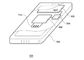
続いて同期整流回路100の好ましい用途を説明する。図5は、図2の同期整流回路100を備えるワイヤレス受電装置300のブロック図である。ワイヤレス受電装置300は、受信コイルLRX、共振キャパシタCs,Cd、平滑キャパシタCRECT(104)および受電制御IC400を備える。同期整流回路100は、受電制御IC400に集積化されている。受電制御IC400は、同期整流回路100に加えて、レギュレータ310、コントローラ312、変調器314を備える。同期整流回路100は、受信コイル302に流れる電流を整流する。
(Use)
Next, a preferred application of the
レギュレータ310は、フルブリッジ回路102および平滑キャパシタ104により生成される整流電圧VRECTを安定化し、出力(OUT)ピンから外部へと出力する。
The
コントローラ312は、受電制御IC400全体を統括的に制御するとともに、ワイヤレス送電装置902に送信すべきデータを生成する。このデータには、整流電圧VRECTとその目標値DPの誤差を示すコントロールエラーパケットや、ワイヤレス受電装置300が受信した電力を示すパケットなどを含んでもよい。変調器314はコントローラ312からのデータ(パケット)を変調し、COMM1,COMM2端子を介して受信コイル302に重畳する。
The
ワイヤレス受電装置300は、電磁誘導方式、磁気共鳴方式のいずれに採用してもよい。前者としては、WPC(Wireless power consortium)が策定するQi規格や、Air-Fuel Alliance規格が例示される。Air-Fuel Alliance規格が採用する磁気共鳴方式では、電磁誘導方式の150k〜200kHzよりも高い周波数帯域(たとえば6.78MHz)が用いられる。したがって過電圧保護に関しても、より高速な応答性が求められるため、実施の形態に係る同期整流回路100のメリットをより享受できる可能性がある。あるいは、電気シェーバや電動歯ブラシ、コードレスホン、ゲーム機器のコントローラ、電動工具などに使用される非接触電力伝送(無接点電力伝送、ワイヤレス給電ともいう)に用いることもできる。
The wireless
ワイヤレス受電装置300は電子機器500に搭載される。図6は、ワイヤレス受電装置300を備える電子機器500を示す図である。電子機器500は、携帯電話端末やタブレット端末、ノートPC、デジタルカメラ、デジタルビデオカメラ、ポータブルオーディオ機器、ポータブルゲーム機器などであってもよい。
The wireless
電子機器500の筐体502には、受信コイルLRXや受電制御IC400に加えて、充電回路504や二次電池506が収容される。充電回路504は、受電制御IC400の出力電圧VOUTを受け、二次電池506を充電する。なお、これらの部品のレイアウトは特に限定されない。
The
以上、本発明について、実施の形態をもとに説明した。これらの実施の形態は例示であり、それらの各構成要素や各処理プロセスの組み合わせにいろいろな変形例が可能なこと、またそうした変形例も本発明の範囲にあることは当業者に理解されるところである。以下、こうした変形例について説明する。 The present invention has been described based on the embodiments. Those skilled in the art will understand that these embodiments are exemplifications, and that various modifications can be made to combinations of the respective constituent elements and processing processes, and such modifications are also within the scope of the present invention. By the way. Hereinafter, such modifications will be described.
(第1変形例)
実施の形態では過電圧状態において、第1トランジスタM1〜第4トランジスタM4のすべてのゲート信号を遅延させたが、本発明はそれに限定されない。たとえばタイミング制御部206は、ローサイド側の2個のトランジスタM3,M4のゲート信号を遅延させてもよい。さらに言えば、過電圧状態において、理想的なゼロカレントスイッチングから遠ざければよいため、少なくともひとつのゲート信号を遅延させてもよい。
(First modification)
In the embodiment, all the gate signals of the first transistor M1 to the fourth transistor M4 are delayed in the overvoltage state, but the present invention is not limited to this. For example, the
あるいは、タイミング制御部206は、過電圧状態において、各トランジスタのスイッチングタイミングを、ゼロカレントスイッチングの理想タイミングよりも、早めてもよい。
Alternatively, the
(第2変形例)
過電圧検出信号SOVPがアサートされたときの、スイッチングのタイミングの変化量、たとえば遅延量τOVPは、整流ライン106の電圧VRECTの傾きに応じていてもよい。電圧VRECTの傾きが大きいほど遅延量τOVPを大きくすることで、適応的な過電圧保護が実現できる。電圧VRECTの傾きは、ハイパスフィルタ(微分回路)を利用して検出してもよいし、A/Dコンバータで取り込んだデジタル値から計算してもよい。
(Second modification)
The amount of change in switching timing when the overvoltage detection signal S OVP is asserted, for example, the delay amount τ OVP , may depend on the slope of the voltage V RECT of the rectifying
(第3変形例)
過電圧検出信号SOVPがアサートされたときのスイッチングのタイミングの変化量、たとえば遅延量τOVPは、整流ライン106の電圧レベルVRECTに応じていてもよい。整流電圧VRECTが高いほど遅延量τOVPを大きくすることで、適応的な過電圧保護が実現できる。整流電圧VRECTの電圧レベルは、A/Dコンバータで取り込んでもよいし、しきい値が異なる複数のOVPコンパレータを併用して検出してもよい。
(Third Modification)
The amount of change in switching timing when the overvoltage detection signal S OVP is asserted, for example, the delay amount τ OVP , may depend on the voltage level V RECT of the rectifying
(第4変形例)
実施の形態では、フルブリッジ回路102が制御回路200と同一のICに集積化される場合を説明したが、大電力のアプリケーションでは、フルブリッジ回路102のトランジスタM1〜M4としてディスクリート素子を用いてもよい。
(Fourth modification)
In the embodiment, the case where the
(第5変形例)
実施の形態では、しきい値電圧VZC1〜VZC4をゼロ近傍としたが、整流電圧VRECT側に設定してもよい。
(5th modification)
In the embodiment, the threshold voltage V ZC1 ~V ZC4 was near zero, may be set to the rectified voltage V RECT side.
(第6変形例)
実施の形態に係る同期整流回路100は、電力信号の周波数が、商用交流よりも高いワイヤレス給電の整流回路として好適に使用できる。なお同期整流回路100の用途はこれには限定されず、AC/DCコンバータなどさまざまな用途に利用しうる。
(Sixth Modification)
The
実施の形態にもとづき、具体的な用語を用いて本発明を説明したが、実施の形態は、本発明の原理、応用を示しているにすぎず、実施の形態には、請求の範囲に規定された本発明の思想を逸脱しない範囲において、多くの変形例や配置の変更が認められる。 Although the present invention has been described using specific terms based on the embodiments, the embodiments only illustrate the principles and applications of the present invention, and the embodiments are defined in the claims. Many variations and modifications of the arrangement are permitted without departing from the spirit of the present invention.
100…同期整流回路、102…フルブリッジ回路、104…平滑キャパシタ、106…整流ライン、108…接地ライン、200…制御回路、202…ゼロカレント検出回路、204…制御ロジック、206…タイミング制御部、208…ドライバ、210…OVPコンパレータ、300…ワイヤレス受電装置、LRX…受信コイル、Cs,Cd…共振キャパシタ、310…レギュレータ、312…コントローラ、314…変調器、400…受電制御IC、500…電子機器、502…筐体、504…充電回路、506…二次電池、M1…第1トランジスタ、M2…第2トランジスタ、M3…第3トランジスタ、M4…第4トランジスタ。
DESCRIPTION OF
Claims (13)
前記制御回路は、
前記フルブリッジ回路が接続される第1交流入力および第2交流入力の電圧の少なくともひとつをしきい値電圧と比較し、比較結果を示す少なくともひとつの検出信号を生成するゼロカレント検出回路と、
前記少なくともひとつの検出信号に応じて、前記フルブリッジ回路を構成する4個のトランジスタのオン、オフを指示する4個の制御信号を生成する制御ロジックと、
前記フルブリッジ回路の整流ラインの電圧が過電圧しきい値電圧を超えると過電圧検出信号をアサートする過電圧検出コンパレータと、
前記過電圧検出信号のアサートに応答して前記4個のトランジスタの少なくともひとつのスイッチングタイミングを、前記制御信号の指示するタイミングと異ならしめるタイミング制御部と、
を備えることを特徴とする制御回路。 A control circuit that is used in a wireless power receiving apparatus and that forms a synchronous rectifier circuit together with a full bridge circuit,
The control circuit includes:
A zero current detection circuit that compares at least one of the voltages of the first AC input and the second AC input to which the full bridge circuit is connected with a threshold voltage and generates at least one detection signal indicating the comparison result;
In response to the at least one detection signal, a control logic that generates four control signals for instructing on and off of the four transistors constituting the full bridge circuit;
An overvoltage detection comparator that asserts an overvoltage detection signal when the voltage of the rectification line of the full bridge circuit exceeds an overvoltage threshold voltage;
A timing control section that makes the switching timing of at least one of the four transistors different from the timing indicated by the control signal in response to the assertion of the overvoltage detection signal;
A control circuit comprising:
前記フルブリッジ回路を制御する請求項1から8のいずれかに記載の制御回路と、
を備え、受信コイルの電流を整流することを特徴とする同期整流回路。 Full bridge circuit,
The control circuit according to any one of claims 1 to 8, which controls the full bridge circuit;
A synchronous rectifier circuit characterized by rectifying the current of the receiving coil.
受信コイルと接続されるフルブリッジ回路を制御する請求項1から8のいずれかに記載の制御回路と、
前記フルブリッジ回路により生成される整流電圧を安定化するレギュレータと、
ワイヤレス送電装置に送信すべきデータを生成するコントローラと、
前記データを変調し、前記受信コイルに重畳する変調器と、
を備えることを特徴とする受電制御回路。 A power reception control circuit used in a wireless power receiving apparatus,
The control circuit according to any one of claims 1 to 8, which controls a full bridge circuit connected to the receiving coil;
A regulator for stabilizing a rectified voltage generated by the full bridge circuit;
A controller that generates data to be transmitted to the wireless power transmission device;
A modulator that modulates the data and superimposes the data on the receiving coil;
A power reception control circuit comprising:
前記受信コイルと接続されるフルブリッジ回路と、
前記フルブリッジ回路と接続される平滑キャパシタと、
前記フルブリッジ回路を制御する請求項1から8のいずれかに記載の制御回路と、
前記平滑キャパシタに生ずる整流電圧を安定化するレギュレータと、
を備えることを特徴とするワイヤレス受電装置。 A receiving coil;
A full bridge circuit connected to the receiving coil;
A smoothing capacitor connected to the full bridge circuit;
The control circuit according to any one of claims 1 to 8, which controls the full bridge circuit;
A regulator for stabilizing a rectified voltage generated in the smoothing capacitor;
A wireless power receiving apparatus comprising:
前記フルブリッジ回路の第1交流入力および第2交流入力の電圧にもとづき、前記フルブリッジ回路をソフトスイッチングさせることができるタイミングで遷移する4個の制御信号を生成するステップと、
前記4個の制御信号にもとづいて前記フルブリッジ回路を駆動するステップと、
前記フルブリッジ回路の出力である整流電圧が過電圧しきい値電圧を超えると、前記4個の制御信号の少なくともひとつを遅延させて、前記フルブリッジ回路を非ソフトスイッチング動作させるステップと、
を備えることを特徴とする制御方法。 A control method of a full bridge circuit for rectifying a current flowing in a receiving coil of a wireless power receiving apparatus,
Generating four control signals that transition at a timing at which the full bridge circuit can be soft-switched based on voltages of the first AC input and the second AC input of the full bridge circuit;
Driving the full bridge circuit based on the four control signals;
When the rectified voltage, which is the output of the full bridge circuit, exceeds an overvoltage threshold voltage, delaying at least one of the four control signals to cause the full bridge circuit to perform a non-soft switching operation;
A control method comprising:
Priority Applications (1)
| Application Number | Priority Date | Filing Date | Title |
|---|---|---|---|
| JP2016082074A JP6711679B2 (en) | 2016-04-15 | 2016-04-15 | Synchronous rectification circuit of wireless power receiving device, control circuit thereof, control method, wireless power receiving device and power receiving control circuit, electronic device |
Applications Claiming Priority (1)
| Application Number | Priority Date | Filing Date | Title |
|---|---|---|---|
| JP2016082074A JP6711679B2 (en) | 2016-04-15 | 2016-04-15 | Synchronous rectification circuit of wireless power receiving device, control circuit thereof, control method, wireless power receiving device and power receiving control circuit, electronic device |
Publications (2)
| Publication Number | Publication Date |
|---|---|
| JP2017192261A true JP2017192261A (en) | 2017-10-19 |
| JP6711679B2 JP6711679B2 (en) | 2020-06-17 |
Family
ID=60086088
Family Applications (1)
| Application Number | Title | Priority Date | Filing Date |
|---|---|---|---|
| JP2016082074A Active JP6711679B2 (en) | 2016-04-15 | 2016-04-15 | Synchronous rectification circuit of wireless power receiving device, control circuit thereof, control method, wireless power receiving device and power receiving control circuit, electronic device |
Country Status (1)
| Country | Link |
|---|---|
| JP (1) | JP6711679B2 (en) |
Cited By (2)
| Publication number | Priority date | Publication date | Assignee | Title |
|---|---|---|---|---|
| KR20200010466A (en) * | 2018-06-27 | 2020-01-30 | 칩원 테크놀로지(베이징) 컴퍼니 리미티드 | LED drive controller, LED drive circuit and LED light emitting device |
| JP2020178442A (en) * | 2019-04-18 | 2020-10-29 | ローム株式会社 | Control circuit of wireless power reception device, electronic apparatus, and control method of wireless power reception device |
Citations (10)
| Publication number | Priority date | Publication date | Assignee | Title |
|---|---|---|---|---|
| JPH09219938A (en) * | 1995-12-05 | 1997-08-19 | Denso Corp | Power generating equipment for automobile |
| JP2000152633A (en) * | 1998-11-16 | 2000-05-30 | Omron Corp | Power unit |
| JP2004032980A (en) * | 1998-05-18 | 2004-01-29 | Seiko Epson Corp | Overcharge-preventing method, circuit for charging, and electronic equipment and time-piece |
| JP2004248342A (en) * | 2003-02-10 | 2004-09-02 | Sanyo Electric Co Ltd | System interconnection power generation system, control method, control program and recording medium |
| JP2006174636A (en) * | 2004-12-17 | 2006-06-29 | Fuji Electric Systems Co Ltd | Auxiliary power unit |
| JP2006174836A (en) * | 1993-08-30 | 2006-07-06 | Baylor College Medicine | Senescent cell-derived dna synthesis-inhibiting factor |
| JP2012044489A (en) * | 2010-08-20 | 2012-03-01 | Fujitsu Semiconductor Ltd | Skew adjusting circuit |
| JP2012235669A (en) * | 2010-11-19 | 2012-11-29 | Rohm Co Ltd | Switching rectification circuit and battery charger using the same |
| US20140265610A1 (en) * | 2013-03-13 | 2014-09-18 | Integrated Device Technology, Inc. | Apparatuses and related methods for modulating power of a wireless power receiver |
| JP2016025702A (en) * | 2014-07-17 | 2016-02-08 | ローム株式会社 | Wireless power reception device, receiver circuit thereof and control method for wireless power reception device |
-
2016
- 2016-04-15 JP JP2016082074A patent/JP6711679B2/en active Active
Patent Citations (10)
| Publication number | Priority date | Publication date | Assignee | Title |
|---|---|---|---|---|
| JP2006174836A (en) * | 1993-08-30 | 2006-07-06 | Baylor College Medicine | Senescent cell-derived dna synthesis-inhibiting factor |
| JPH09219938A (en) * | 1995-12-05 | 1997-08-19 | Denso Corp | Power generating equipment for automobile |
| JP2004032980A (en) * | 1998-05-18 | 2004-01-29 | Seiko Epson Corp | Overcharge-preventing method, circuit for charging, and electronic equipment and time-piece |
| JP2000152633A (en) * | 1998-11-16 | 2000-05-30 | Omron Corp | Power unit |
| JP2004248342A (en) * | 2003-02-10 | 2004-09-02 | Sanyo Electric Co Ltd | System interconnection power generation system, control method, control program and recording medium |
| JP2006174636A (en) * | 2004-12-17 | 2006-06-29 | Fuji Electric Systems Co Ltd | Auxiliary power unit |
| JP2012044489A (en) * | 2010-08-20 | 2012-03-01 | Fujitsu Semiconductor Ltd | Skew adjusting circuit |
| JP2012235669A (en) * | 2010-11-19 | 2012-11-29 | Rohm Co Ltd | Switching rectification circuit and battery charger using the same |
| US20140265610A1 (en) * | 2013-03-13 | 2014-09-18 | Integrated Device Technology, Inc. | Apparatuses and related methods for modulating power of a wireless power receiver |
| JP2016025702A (en) * | 2014-07-17 | 2016-02-08 | ローム株式会社 | Wireless power reception device, receiver circuit thereof and control method for wireless power reception device |
Cited By (4)
| Publication number | Priority date | Publication date | Assignee | Title |
|---|---|---|---|---|
| KR20200010466A (en) * | 2018-06-27 | 2020-01-30 | 칩원 테크놀로지(베이징) 컴퍼니 리미티드 | LED drive controller, LED drive circuit and LED light emitting device |
| KR102279464B1 (en) * | 2018-06-27 | 2021-07-21 | 칩원 테크놀로지(베이징) 컴퍼니 리미티드 | LED drive controller, LED drive circuit and LED light emitting device |
| JP2020178442A (en) * | 2019-04-18 | 2020-10-29 | ローム株式会社 | Control circuit of wireless power reception device, electronic apparatus, and control method of wireless power reception device |
| JP7256677B2 (en) | 2019-04-18 | 2023-04-12 | ローム株式会社 | Control circuits for wireless power receivers, electronic devices |
Also Published As
| Publication number | Publication date |
|---|---|
| JP6711679B2 (en) | 2020-06-17 |
Similar Documents
| Publication | Publication Date | Title |
|---|---|---|
| JP6554317B2 (en) | Synchronous rectifier circuit, control circuit therefor, wireless power receiver and electronic device | |
| US10734817B2 (en) | Method for wireless power transfer using a power converter with a bypass mode | |
| US10218283B2 (en) | Insulated synchronous rectification DC/DC converter | |
| CN110022068B (en) | Synchronous rectification gate driver with active clamper | |
| TWI509931B (en) | Wireless power receiving and supplying apparatus, wireless power supply system and auto-adjusting assistant circuit | |
| JP5764082B2 (en) | Wireless power receiving device, wireless power feeding device, and wireless power transmission system | |
| WO2017042987A1 (en) | Wireless power transmission system and power transmission device | |
| CN108206634B (en) | Insulating synchronous rectification DC/DC converter, controller, adapter and equipment | |
| JPWO2017145602A1 (en) | Wireless power transmission apparatus, control method therefor, power transmission control circuit, charger | |
| JP2017212858A (en) | Wireless power reception device and control method thereof, power reception control circuit, and electronic apparatus | |
| JP6632308B2 (en) | Wireless power transmission device, control circuit and control method thereof, and charger | |
| US9356521B2 (en) | Switching power-supply device having wide input voltage range | |
| US9356519B2 (en) | Current balance circuit of resonant type switching power-supply circuit | |
| KR20120031812A (en) | Duty balancing oscilator | |
| US20200052527A1 (en) | Power transmitter and method for wirelessly transferring power | |
| JPWO2015125655A1 (en) | Power receiving apparatus, power supply control method, and power supply system | |
| KR20230103963A (en) | Pwm control of analog front end | |
| US10840742B2 (en) | Wireless power receiver synchronization detection circuit | |
| JP6711679B2 (en) | Synchronous rectification circuit of wireless power receiving device, control circuit thereof, control method, wireless power receiving device and power receiving control circuit, electronic device | |
| TW202107809A (en) | Switching power converters, and the primary-side controllers and methods of controlling same | |
| US11316435B2 (en) | Insulated DC/DC converter, AC/DC converter, power adapter, and electric device | |
| WO2018116621A1 (en) | Gate driving device | |
| JP7256677B2 (en) | Control circuits for wireless power receivers, electronic devices | |
| JP2021019449A (en) | Control ic of wireless power reception device, electronic apparatus, and modulation method in wireless power reception device | |
| KR20070020422A (en) | Switch mode power supply with output voltage equalizer |
Legal Events
| Date | Code | Title | Description |
|---|---|---|---|
| A621 | Written request for application examination |
Free format text: JAPANESE INTERMEDIATE CODE: A621 Effective date: 20190225 |
|
| A131 | Notification of reasons for refusal |
Free format text: JAPANESE INTERMEDIATE CODE: A131 Effective date: 20200107 |
|
| A977 | Report on retrieval |
Free format text: JAPANESE INTERMEDIATE CODE: A971007 Effective date: 20191226 |
|
| A521 | Request for written amendment filed |
Free format text: JAPANESE INTERMEDIATE CODE: A523 Effective date: 20200306 |
|
| TRDD | Decision of grant or rejection written | ||
| A01 | Written decision to grant a patent or to grant a registration (utility model) |
Free format text: JAPANESE INTERMEDIATE CODE: A01 Effective date: 20200519 |
|
| A61 | First payment of annual fees (during grant procedure) |
Free format text: JAPANESE INTERMEDIATE CODE: A61 Effective date: 20200528 |
|
| R150 | Certificate of patent or registration of utility model |
Ref document number: 6711679 Country of ref document: JP Free format text: JAPANESE INTERMEDIATE CODE: R150 |
|
| R250 | Receipt of annual fees |
Free format text: JAPANESE INTERMEDIATE CODE: R250 |