JP2017010726A - Display device - Google Patents
Display device Download PDFInfo
- Publication number
- JP2017010726A JP2017010726A JP2015124169A JP2015124169A JP2017010726A JP 2017010726 A JP2017010726 A JP 2017010726A JP 2015124169 A JP2015124169 A JP 2015124169A JP 2015124169 A JP2015124169 A JP 2015124169A JP 2017010726 A JP2017010726 A JP 2017010726A
- Authority
- JP
- Japan
- Prior art keywords
- layer
- electrode
- display device
- electrode pattern
- color filter
- Prior art date
- Legal status (The legal status is an assumption and is not a legal conclusion. Google has not performed a legal analysis and makes no representation as to the accuracy of the status listed.)
- Pending
Links
- 238000005192 partition Methods 0.000 claims abstract description 27
- 239000003086 colorant Substances 0.000 claims abstract description 4
- 229910052751 metal Inorganic materials 0.000 claims description 15
- 239000002184 metal Substances 0.000 claims description 15
- 239000004020 conductor Substances 0.000 claims description 6
- 239000000758 substrate Substances 0.000 abstract description 29
- 239000000203 mixture Substances 0.000 abstract description 2
- 239000010410 layer Substances 0.000 description 148
- 239000000463 material Substances 0.000 description 12
- 229910052581 Si3N4 Inorganic materials 0.000 description 11
- 238000005401 electroluminescence Methods 0.000 description 11
- HQVNEWCFYHHQES-UHFFFAOYSA-N silicon nitride Chemical compound N12[Si]34N5[Si]62N3[Si]51N64 HQVNEWCFYHHQES-UHFFFAOYSA-N 0.000 description 11
- 239000011159 matrix material Substances 0.000 description 9
- 230000003287 optical effect Effects 0.000 description 7
- 239000012044 organic layer Substances 0.000 description 7
- 230000002093 peripheral effect Effects 0.000 description 7
- 238000000034 method Methods 0.000 description 6
- 230000000694 effects Effects 0.000 description 5
- 230000004048 modification Effects 0.000 description 5
- 238000012986 modification Methods 0.000 description 5
- 239000010408 film Substances 0.000 description 4
- 238000007639 printing Methods 0.000 description 3
- ZOKXTWBITQBERF-UHFFFAOYSA-N Molybdenum Chemical compound [Mo] ZOKXTWBITQBERF-UHFFFAOYSA-N 0.000 description 2
- RTAQQCXQSZGOHL-UHFFFAOYSA-N Titanium Chemical compound [Ti] RTAQQCXQSZGOHL-UHFFFAOYSA-N 0.000 description 2
- 229910052782 aluminium Inorganic materials 0.000 description 2
- XAGFODPZIPBFFR-UHFFFAOYSA-N aluminium Chemical compound [Al] XAGFODPZIPBFFR-UHFFFAOYSA-N 0.000 description 2
- -1 for example Substances 0.000 description 2
- 230000005525 hole transport Effects 0.000 description 2
- 229910052750 molybdenum Inorganic materials 0.000 description 2
- 239000011733 molybdenum Substances 0.000 description 2
- 230000035945 sensitivity Effects 0.000 description 2
- 229910052719 titanium Inorganic materials 0.000 description 2
- 239000010936 titanium Substances 0.000 description 2
- WFKWXMTUELFFGS-UHFFFAOYSA-N tungsten Chemical compound [W] WFKWXMTUELFFGS-UHFFFAOYSA-N 0.000 description 2
- 229910052721 tungsten Inorganic materials 0.000 description 2
- 239000010937 tungsten Substances 0.000 description 2
- QNRATNLHPGXHMA-XZHTYLCXSA-N (r)-(6-ethoxyquinolin-4-yl)-[(2s,4s,5r)-5-ethyl-1-azabicyclo[2.2.2]octan-2-yl]methanol;hydrochloride Chemical compound Cl.C([C@H]([C@H](C1)CC)C2)CN1[C@@H]2[C@H](O)C1=CC=NC2=CC=C(OCC)C=C21 QNRATNLHPGXHMA-XZHTYLCXSA-N 0.000 description 1
- 238000010586 diagram Methods 0.000 description 1
- 239000011521 glass Substances 0.000 description 1
- AMGQUBHHOARCQH-UHFFFAOYSA-N indium;oxotin Chemical compound [In].[Sn]=O AMGQUBHHOARCQH-UHFFFAOYSA-N 0.000 description 1
- 239000011810 insulating material Substances 0.000 description 1
- 238000010030 laminating Methods 0.000 description 1
- 238000007644 letterpress printing Methods 0.000 description 1
- 238000000059 patterning Methods 0.000 description 1
- 238000000206 photolithography Methods 0.000 description 1
- 238000005215 recombination Methods 0.000 description 1
- 230000006798 recombination Effects 0.000 description 1
- 238000002310 reflectometry Methods 0.000 description 1
- 238000007789 sealing Methods 0.000 description 1
- 229910052709 silver Inorganic materials 0.000 description 1
- 239000004332 silver Substances 0.000 description 1
- 238000000638 solvent extraction Methods 0.000 description 1
- 239000010409 thin film Substances 0.000 description 1
- YVTHLONGBIQYBO-UHFFFAOYSA-N zinc indium(3+) oxygen(2-) Chemical compound [O--].[Zn++].[In+3] YVTHLONGBIQYBO-UHFFFAOYSA-N 0.000 description 1
Images


Classifications
-
- H—ELECTRICITY
- H10—SEMICONDUCTOR DEVICES; ELECTRIC SOLID-STATE DEVICES NOT OTHERWISE PROVIDED FOR
- H10K—ORGANIC ELECTRIC SOLID-STATE DEVICES
- H10K59/00—Integrated devices, or assemblies of multiple devices, comprising at least one organic light-emitting element covered by group H10K50/00
- H10K59/40—OLEDs integrated with touch screens
-
- H—ELECTRICITY
- H10—SEMICONDUCTOR DEVICES; ELECTRIC SOLID-STATE DEVICES NOT OTHERWISE PROVIDED FOR
- H10K—ORGANIC ELECTRIC SOLID-STATE DEVICES
- H10K50/00—Organic light-emitting devices
- H10K50/80—Constructional details
- H10K50/805—Electrodes
- H10K50/81—Anodes
- H10K50/818—Reflective anodes, e.g. ITO combined with thick metallic layers
-
- H—ELECTRICITY
- H10—SEMICONDUCTOR DEVICES; ELECTRIC SOLID-STATE DEVICES NOT OTHERWISE PROVIDED FOR
- H10K—ORGANIC ELECTRIC SOLID-STATE DEVICES
- H10K50/00—Organic light-emitting devices
- H10K50/80—Constructional details
- H10K50/805—Electrodes
- H10K50/82—Cathodes
- H10K50/828—Transparent cathodes, e.g. comprising thin metal layers
-
- H—ELECTRICITY
- H10—SEMICONDUCTOR DEVICES; ELECTRIC SOLID-STATE DEVICES NOT OTHERWISE PROVIDED FOR
- H10K—ORGANIC ELECTRIC SOLID-STATE DEVICES
- H10K59/00—Integrated devices, or assemblies of multiple devices, comprising at least one organic light-emitting element covered by group H10K50/00
- H10K59/30—Devices specially adapted for multicolour light emission
- H10K59/38—Devices specially adapted for multicolour light emission comprising colour filters or colour changing media [CCM]
Landscapes
- Physics & Mathematics (AREA)
- Optics & Photonics (AREA)
- Electroluminescent Light Sources (AREA)
- Optical Filters (AREA)
Abstract
Description
本発明は、表示装置に関する。 The present invention relates to a display device.
従来、有機EL(Electro Luminescence)表示装置においては、カラーフィルタ層を構成する複数の着色層が、有機EL素子を覆う封止層上に、単位画素毎に区分されて形成される構成が知られている(例えば、特許文献1参照)。 2. Description of the Related Art Conventionally, in an organic EL (Electro Luminescence) display device, a configuration in which a plurality of colored layers constituting a color filter layer is formed separately for each unit pixel on a sealing layer covering an organic EL element is known. (For example, refer to Patent Document 1).
ここで、着色層が互いに隣接して形成される場合、単位画素間において光の混色が生じるおそれがある。 Here, when the colored layers are formed adjacent to each other, there is a possibility that color mixture of light occurs between the unit pixels.
上記課題に鑑みて、本発明は、単位画素間における光の混色を抑制する表示装置を提供することを目的とする。 In view of the above problems, an object of the present invention is to provide a display device that suppresses color mixing of light between unit pixels.
本発明の一態様は、画像を構成する複数の単位画素それぞれで輝度が制御されて発光する発光素子層と、複数色の着色層を有し、いずれかの色の前記着色層がいずれかの前記単位画素に対応するカラーフィルタ層と、少なくとも1層からなる絶縁層と、タッチ入力を検出するために前記絶縁層の両面にそれぞれ設けられた第1電極及び第2電極と、を有し、隣同士の前記着色層は、隔壁によって区画され、前記隔壁は、高さ方向の少なくとも一部が、前記第1電極によって構成されていることを特徴とする。 One embodiment of the present invention includes a light-emitting element layer that emits light with controlled brightness in each of a plurality of unit pixels that form an image, and a plurality of colored layers. A color filter layer corresponding to the unit pixel, an insulating layer composed of at least one layer, and a first electrode and a second electrode respectively provided on both surfaces of the insulating layer to detect touch input; The colored layers adjacent to each other are partitioned by partition walls, and at least a part of the partition walls in the height direction is configured by the first electrodes.
以下に、本発明の各実施形態について、図面を参照しつつ説明する。なお、開示はあくまで一例にすぎず、当業者において、発明の主旨を保っての適宜変更について容易に想到し得るものについては、当然に本発明の範囲に含有されるものである。また、図面は説明をより明確にするため、実際の態様に比べ、各部の幅、厚さ、形状等について模式的に表される場合があるが、あくまで一例であって、本発明の解釈を限定するものではない。また、本明細書と各図において、既出の図に関して前述したものと同様の要素には、同一の符号を付して、詳細な説明を適宜省略することがある。 Embodiments of the present invention will be described below with reference to the drawings. It should be noted that the disclosure is merely an example, and those skilled in the art can easily conceive of appropriate modifications while maintaining the gist of the invention are naturally included in the scope of the present invention. In addition, the drawings may be schematically represented with respect to the width, thickness, shape, and the like of each part in comparison with actual aspects for the sake of clarity of explanation, but are merely examples, and the interpretation of the present invention is not limited. It is not limited. In addition, in the present specification and each drawing, elements similar to those described above with reference to the previous drawings are denoted by the same reference numerals, and detailed description may be omitted as appropriate.
まず、図1〜図6を参照して、第1実施形態に係る有機EL(Electro Luminescence)表示装置(以下、単に表示装置という)100について説明する。表示装置100は、第1電極パターン6と第2電極パターン9を有し、ユーザが画面上の表示を押すことによる第1電極パターン6の電極6a(第1電極)と第2電極パターン9の電極9a(第2電極)の間の静電容量の変化を検出し、機器を操作可能とするタッチ入力式の表示装置である。
First, an organic EL (Electro Luminescence) display device (hereinafter simply referred to as a display device) 100 according to the first embodiment will be described with reference to FIGS. The
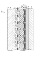
図1は、第1実施形態に係る表示装置100の構成を示す模式断面図である。表示装置100は、回路層側基板1と、回路層2と、発光素子層3と、下地層4と、カラーフィルタ層5と、第1電極パターン6と、充填層7と、対向基板8と、第2電極パターン9とを有し、それらが積層して構成される。
FIG. 1 is a schematic cross-sectional view illustrating a configuration of a
回路層側基板1は透明なガラスからなる。回路層2は回路層側基板1上に形成される。回路層2は、詳細な構成に関しては図1においては省略するが、発光素子層3の発光を制御する薄膜トランジスタがマトリクス状に多数配列された基板である。
The circuit layer side substrate 1 is made of transparent glass. The
発光素子層3は、下部電極31と、発光する有機EL層32と、上部電極33と、ITO(Indium Tin Oxide、酸化インジウムスズ)層34と、反射層35と、バンク層36とを有し、画素を構成する複数の単位画素(副画素)それぞれで輝度が制御されて発光する。ITO層34は、回路層2上に形成される透明導電層である。反射層35は、ITO層34上に形成され、銀等の金属からなる層である。
The light
なお、第1実施形態においては、一つの画素は複数の副画素で構成されている。発色の異なる副画素が複数集まって一画素が構成され、表示装置100のカラー表示を可能としている。
In the first embodiment, one pixel is composed of a plurality of subpixels. A plurality of sub-pixels having different colors are collected to form one pixel, which enables the
図1においては簡略化して図示するが、有機EL層32は、カソード側からアノード側に向けて順に、電子輸送層、発光層、ホール輸送層が積層して構成される。下部電極31は、アノードとして機能し、ITOからなる。上部電極33は、カソードとして機能し、IZO(Indium Zinc Oxide、酸化インジウム亜鉛)からなる。
Although simplified in FIG. 1, the
下部電極31と上部電極33に直流電圧が印加されると、下部電極31側から注入されたホールがホール輸送層を経由し、一方、上部電極33側から注入された電子が電子輸送層を経由して、それぞれ有機EL層32に到達し、電子とホールが再結合する。このような電子とホールの再結合により、発光素子層3は所定の波長の発光を行う。下部電極31は、発光領域となる部分を覆うように形成される。また、バンク層36は、非発光領域となる部分に形成される。有機EL層32は、下部電極31を覆うように形成されるが、非発光領域では、バンク層36によって下部電極31から分離される。
When a DC voltage is applied to the
有機EL層32及び上部電極33は、非発光領域となる部分において、バンク層36の形状に沿った形状となる。また、下地層4は、上部電極33を覆うように形成され、上部電極33(バンク層36)の形状に沿って、上部電極33と面する側の反対側の表面が凸となる。
The
また、第1実施形態においては、タッチ入力を検出する電極の一つである第1電極パターン6の電極6aが下地層4の凸部4a上にそれぞれ形成される。
In the first embodiment, the
また、カラーフィルタ層5は複数色の着色層を有し、いずれかの色の着色層がいずれかの単位画素に対応するように下地層4上に形成される。第1実施形態においては、カラーフィルタ層5は、白色の着色層5W、赤色の着色層5R、緑色の着色層5G、青色の着色層5Bを有する。
The
着色層5W、5R、5G、5Bは、下地層4の凸部4a間にそれぞれ形成され、隣同士の着色層は隔壁によって区画されている。第1実施形態においては、下地層4の凸部4aが隔壁の下部を形成し、第1電極パターン6が隔壁の上部を形成する。また、図1に示すように、隔壁の高さは着色層の高さと略同じであり、隣同士の着色層は隔壁により分離されている。
The
着色層5W、5R、5G、5Bは、インクジェットを用いた印刷方式により形成される。第1実施形態においては、各色の着色層の材料が充填される領域は、隔壁により区画されているため、着色層の充填時に各着色層の材料が混ざり合うことがない。
The
さらに、第1電極パターン6上には遮光膜として機能するブラックマトリックスBMが形成される。そのため、隣同士の着色層間(副画素間)において光が遮光され、光学的な混色が抑制される。なお、図1に示すように、ブラックマトリックスBMは、隣り合う着色層を掛け渡すように形成される。
Further, a black matrix BM that functions as a light shielding film is formed on the
さらに、充填層7がカラーフィルタ層5及び第1電極パターン6を覆うように形成され、充填層7上には対向基板8が積層される。充填層7及び対向基板8は、透明絶縁材料からなる。なお、第1実施形態の充填層7及び対向基板8が本発明の絶縁層に対応する構成であり、充填層7が絶縁層の第1層に対応し、対向基板8が絶縁層の第2層に対応する。
Further, the
対向基板8上には第2電極パターン9が設けられる。ユーザが画面にタッチすると、第2電極パターン9の電極9aと第1電極パターン6の電極6aでタッチ入力が検出され、機器の操作が行われる。なお、第1実施形態においては、電極9aは透明導電材料からなる。本発明においては電極6aは透明導電材料で形成される必要は無く、金属の配線でもよい。第1電極パターン6の上にはブラックマトリクスBMが配置され、金属配線による外光の反射を防止している。なお、透明導電材料としては、例えば、ITOを用いるとよい。
A
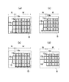
ここで、図2、図3を参照して、第1電極パターン6の構成について説明する。図2は、第1実施形態に係る表示装置の概要を示す斜視図である。図3は、図2の領域A周辺の拡大図であって、第1電極パターンの様々な配列を示す図である。
Here, the configuration of the
表示装置100の積層構造は図1で説明した通りであり、図2においては、説明の便宜上、回路層側基板1、回路層2、発光素子層3、及び下地層4を含む基板101と、充填層7及び対向基板8を含む基板102と、第1電極パターン6のみを示し、第2電極パターン9等については省略する。第1電極パターン6は、基板101と基板102の間に形成されている。
The stacked structure of the
表示装置100は、マトリクス状に設けられる複数の副画素を含む表示領域Mと、表示領域Mの周辺の周辺領域Nを有する。表示領域Mに対応する領域には第1電極が設けられる。
The
図2に示すように、周辺領域Nには、電極6aと電気的に接続される配線6cが設けられている。配線6cは複数本設けられ、それらの端部はの端子に接続される。なお、配線6cが接続される端子にはのフレキシブル配線基板が接続される。
As shown in FIG. 2, the peripheral region N is provided with a
ここで、電極6aの配列の詳細について説明するが、まず、図3(a)を参照して、電極6aの一の配列パターンについて説明する。図3(a)に示すように、第1電極パターン6は、一方向に延び、略等間隔に複数本設けられる細線状の電極6aを有する。そして、電極6aは、表示領域Mの周辺の周辺領域Nに設けられる配線6cと電気的に接続される。また、複数の電極6a間の領域には、電極6aと直交する方向に延び、短い線状の電極6bが略等間隔で配列されている。電極6bを設けることにより、電極6a間の空白領域が埋められ、ユーザが表示領域Mを斜めから見た場合であっても、電極6aが縞状に視認されることが抑制される。
Here, details of the arrangement of the
複数の電極6aの間隔と、複数の電極6bの間隔は、隣り合う一対の電極6aと隣り合う一対の電極6bとで1つの副画素を囲むような間隔であることが好ましい。言い換えると、隣り合う一対の電極6aと、隣り合う一対の電極6bとの4つの電極で囲まれる領域が1つの副画素に対応する領域となる。
The interval between the plurality of
なお、図3(a)で示した第1電極パターン6の配列は例示であり、この配列に限られるものではない。例えば、第1電極パターン6は、図3(b)〜図3(d)に示すような配列であってもよい。
The arrangement of the
すなわち、図3(b)に示すように、配線6cに接続される電極6aを間引いた構成としてもよい。このように、配線6cに接続される電極6aの本数を調整することで、第1電極パターン6の電極6aと第2電極パターン9の電極9aの間の静電容量を調整することができ、それにより、タッチ入力の感度を調整することができる。
In other words, as shown in FIG. 3B, the
また、図3(c)に示すように、電極6bの一端が電極6aと接続された構成としてもよい。図3(a)の構成においては、1つの副画素を囲む領域において電極6aと電極6bとが離間する箇所が4箇所であるのに対して、図3(c)の構成においては、1つの副画素を囲む領域において電極6aと電極6bとが離間する箇所が2箇所であるため、副画素間の遮光性、反射性が向上する。それにより、副画素間での光学的な混色が抑制される。
Moreover, as shown in FIG.3 (c), it is good also as a structure by which the end of the
また、図3(d)に示すように、図3(c)の構成において、配線6cに接続される電極6aを間引いた構成としてもよい。このような構成を採用することにより、上述のように、タッチ入力の感度の調整を可能にしつつ、副画素間での光学的な混色を抑制できる。
Further, as shown in FIG. 3D, in the configuration of FIG. 3C, the
さらに、図4、図5を参照して、第2電極パターン9の構成について説明する。図4は、図2で示した構成に加えてさらに第2電極パターン9を図示した斜視図であり、図5は、図4の領域Aの拡大図であって、第1電極パターン6及び第2電極パターン9の様々な配列を示す図である。なお、第2電極パターン9は、基板102上に形成されている。
Further, the configuration of the
図5(a)は、図3(a)で示した第1電極パターン6上に第2電極パターン9が配置された状態を示しており、図5(b)は、図3(c)で示した第1電極パターン6上に第2電極パターン9が配置された状態を示している。
FIG. 5A shows a state in which the
電極9aは、周辺領域Nに設けられる配線9cと電気的に接続される。配線9cは複数本設けられ、それらの端部は端子に接続される。なお、配線9cが接続される端子にはフレキシブル配線基板が接続される。また、第2電極パターン9は、第1電極パターン6の電極6aが延びる方向と直交する方向に延びる細線状の電極9bと、複数の副画素を覆う大きさの平面形状が略菱形の電極9aを有している。
The
ここで、電極9a間の空白領域が大きいと、ユーザが表示領域Mを斜めから見たときに、表示ムラが視認されてしまう。そのため、第1実施形態においては、電極9aと同じ材料で端子と電気的に接続されないダミーパターン9dを設けている。ダミーパターン9dを設けることにより、電極9a間の空白領域が埋められ、ユーザが表示領域Mを斜めから見た場合であっても、表示ムラが視認されにくい。
Here, when the blank area between the
以上述べたように、第1実施形態においては、各着色層5W、5R、5G、5Bが、隔壁として機能する第1電極パターン6及び下地層4の凸部4aによって区画されて形成されるため、光学的な混色が抑制される。その結果、コントラストや視認性が向上する。また、隔壁は着色層の材料が充填される領域と略同じ高さ形成されているため、着色層の充填時に隣り合う着色層の材料が混ざり合うことがなく、各着色層は隔壁により分離して形成され、光学的な混色が抑制される。また、タッチ入力を検出するための第1電極パターン6が隔壁としてしての役割を兼ねるため、別途隔壁を構成する部材を設ける必要がなく、装置の薄型化及びコストの抑制を実現できる。
As described above, in the first embodiment, the
図6は、第1実施形態の変形例に係る表示装置を示す模式断面図である。図1においては、第2電極パターン9が対向基板8の上面に形成される構成について説明したが、図6に示すように、第2電極パターン9を対向基板8の下面に形成する構成であってもよい。このように、タッチ入力を検出するための第1電極パターン6及び第2電極パターン9が、絶縁層としての充填層7の両面にそれぞれ設けられる構成であっても、第1実施形態で説明した効果と同様の効果を得ることができる。
FIG. 6 is a schematic cross-sectional view showing a display device according to a modification of the first embodiment. In FIG. 1, the configuration in which the
次に、図7〜図9を参照して、第2実施形態に係る表示装置について説明する。 Next, the display device according to the second embodiment will be described with reference to FIGS.
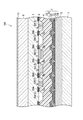
図7は、第2実施形態に係る表示装置を示す模式断面図である。第1実施形態においては第2電極パターンの材料として透明導電材料を用いたが、第2実施形態においては、第2電極パターンの材料として低反射金属を用いる。なお、第2実施形態の第1電極パターン6は、第1実施形態で説明したものと同様とする。また、その他、第1実施形態と同じ構成については同じ符号を用いてその説明は省略する。
FIG. 7 is a schematic cross-sectional view showing a display device according to the second embodiment. In the first embodiment, a transparent conductive material is used as the material of the second electrode pattern. However, in the second embodiment, a low reflection metal is used as the material of the second electrode pattern. The
図7に示すように、第2実施形態に係る表示装置100は、対向基板8上に低反射金属膜としての第2電極パターン19を有する。低反射金属としては、例えば、アルミニウム等と比較して可視広域の反射率の低い金属であるチタン、タングステン、モリブデン等を用いるとよい。低反射金属は、入射された光の一部を反射し、残りの光を吸収する。
As shown in FIG. 7, the
図8は、第2実施形態に係る表示装置の概要を示す斜視図である。図8に示すように、周辺領域Nには、電極19a(第2電極)と電気的に接続される配線19cが設けられている。配線19cは複数本設けられ、それらの端部は不図示の端子に接続される。
FIG. 8 is a perspective view illustrating an outline of a display device according to the second embodiment. As shown in FIG. 8, in the peripheral region N, a
図9は、図8の領域B周辺の拡大図であって、第2電極パターンの様々な配列を示す図である。ここで、第2実施形態の第2電極パターン19の配列の詳細について説明するが、まず、図9(a)を参照して、第2電極パターン19の一の配列パターンについて説明する。図9(a)に示すように、第2電極パターン19は、一方向に延び、略等間隔に複数本設けられる細線状の電極19aを有する。そして、電極19aは、表示領域Mの周辺の周辺領域Nに設けられる配線19cと電気的に接続される。
FIG. 9 is an enlarged view around the region B in FIG. 8 and shows various arrangements of the second electrode pattern. Here, details of the arrangement of the
また、電極19aが配列される間の領域には、電極19aと直交する方向に延び、短い線状の電極19bが略等間隔で配列されている。複数の電極19aの間隔と、複数の電極19bの間隔は、隣り合う一対の電極19aと隣り合う一対の電極19bとで副画素を囲むような間隔であることが好ましい。言い換えると、隣り合う一対の電極19aと、隣り合う一対の電極19bとの4つの電極で囲まれる領域が副画素に対応する領域となる。
In addition, in a region between the
なお、図9(a)で示した第2電極パターン19の配列は例示であり、この配列に限られるものではない。例えば、第2電極パターン19は、図9(b)〜図9(d)に示すような配列であってもよい。
Note that the arrangement of the
すなわち、図9(b)に示すように、配線19cに接続される電極19aを間引いた構成としてもよい。また、図9(c)に示すように、電極19bの一端が電極19aと接続された構成としてもよい。さらに、図9(d)に示すように、図9(c)の構成において、配線19cに接続される電極19aを間引いた構成としてもよい。
That is, as shown in FIG. 9B, the
第2実施形態においては、第2電極パターン19として低反射金属層を用いたことにより、第2電極パターン19の表示領域Mへの映り込みが抑制される。なお、表示領域Mへの映り込みを抑制するため、第1電極パターン6と第2電極パターン19のうち少なくともいずれかに低反射金属層を用いるとよい。
In the second embodiment, the use of the low reflection metal layer as the
図10は、第2実施形態の変形例に係る表示装置を示す模式断面図である。図7においては、第2電極パターン19が対向基板8の上面に形成される構成について説明したが、図10に示すように、第2電極パターン19を対向基板8の下面に形成する構成であってもよい。このように、タッチ入力を検出するための第1電極パターン6及び第2電極パターン19が、絶縁層としての充填層7の両面にそれぞれ設けられる構成であっても、第2実施形態で説明した効果と同様の効果を得ることができる。
FIG. 10 is a schematic cross-sectional view showing a display device according to a modification of the second embodiment. Although the configuration in which the
図11は、第3実施形態に係る表示装置を示す模式断面図である。第1実施形態と同じ構成については同じ符号を用いてその説明は省略する。 FIG. 11 is a schematic cross-sectional view showing a display device according to the third embodiment. About the same structure as 1st Embodiment, the description is abbreviate | omitted using the same code | symbol.
第1実施形態及び第2実施形態においては第1電極パターンの材料として透明導電材料を用いたが、第3実施形態においては、第1電極パターンの材料として低反射金属を用いる。低反射金属としては、例えば、アルミニウム等と比較して可視広域の反射率の低い金属であるチタン、タングステン、モリブデン等を用いるとよい。 In the first and second embodiments, a transparent conductive material is used as the material for the first electrode pattern. In the third embodiment, a low-reflection metal is used as the material for the first electrode pattern. As the low-reflection metal, for example, titanium, tungsten, molybdenum, or the like, which is a metal having a low reflectance in the visible wide range as compared with aluminum or the like, may be used.
第3実施形態においては、低反射金属膜としての第1電極パターン16が、遮光膜としての機能を兼ねるため、別途ブラックマトリックスBMを設ける必要がない。なお、第3実施形態においては、第1電極パターン16の上部にブラックマトリックスBMが形成されない分、第1実施形態及び第2実施形態よりも、第1電極パターン16を高く形成する。図11に示すように、隔壁は着色層の材料が充填される領域よりも高く形成されているため、着色層の充填時に隣り合う着色層の材料が混ざり合うことがなく、各着色層は隔壁により分離して形成され、光学的な混色が抑制される。また、第3実施形態の構成においては、ブラックマトリックスBMを用いない分コストを抑制することができる。
In the third embodiment, since the
図12は、第4実施形態に係る表示装置を示す模式断面図である。第1実施形態と同じ構成については同じ符号を用いてその説明は省略する。 FIG. 12 is a schematic cross-sectional view showing a display device according to the fourth embodiment. About the same structure as 1st Embodiment, the description is abbreviate | omitted using the same code | symbol.
第4実施形態においては、発光素子層3上に下地層14が形成され、さらに下地層14上に第1電極パターン6及びカラーフィルタ層5が形成されている。
In the fourth embodiment, the
第4実施形態においては、下地層14の上面は、平坦面となっている。これは、下地層14が有機層を含む積層構造をとるためである。具体的には、上部電極33上にSiN(窒化ケイ素)層が形成され、SiN層はバンク36層の形状に沿って上面が凸となる。このSiN層上に有機層が形成されている。有機層は、SiN層に面する側はSiN層の凸形状に沿った形状となるが、SiN層に面する側と反対側は平坦面となる。そして、その有機層の平坦面上にさらにSiN層が形成されている。平坦面である有機層上に形成されるSiN層の上面は平坦となる。ここで平坦面とは、上部電極33の凹凸の程度よりも、下地層14の凹凸の程度の方が低減している状態のことを示し、完全に平坦な面でなくてもよい。
In the fourth embodiment, the upper surface of the
以上説明したように、第4実施形態においては、下地層14として、SiN層、有機層、SiN層がこの順で積層された積層構造を有するものを採用した。ただし、そのような積層構造に限られるものではなく、下地層14は、少なくとも1層の有機層を有し、上面が平坦面であればよい。
As described above, in the fourth embodiment, the
下地層14上には、第1電極パターン6が形成される。第4実施形態においては、第1電極パターン6が、隔壁の下部から上部までの全体を構成する。そして、第1電極パターン6で構成される隔壁間に、着色層の材料が充填され、各着色層5W、5R、5G、5Bが隔壁によって区画されて形成される。第4実施形態においては、下地層14の上面が平坦面であるため、他の実施形態と比較して、第1電極パターン6の形成、及び着色層5W、5R、5G、5Bのパターニングが容易となる。
A
図13は、第5実施形態に係る表示装置を示す模式断面図である。第1〜第4実施形態と同じ構成については同じ符号を用いてその説明は省略する。 FIG. 13 is a schematic cross-sectional view showing a display device according to the fifth embodiment. About the same structure as 1st-4th embodiment, the description is abbreviate | omitted using the same code | symbol.
図13に示すように、第5実施形態に係る表示装置100は、第1実施形態で示した充填層7の代わりに透明なカバー層17を有し、かつ対向基板8を有しない構成となっている。すなわち、第5実施形態においては、タッチ入力を検出するための第1電極パターン6及び第2電極パターン19が、絶縁層としてのカバー層7の両面にそれぞれ設けられる構成となっている。
As illustrated in FIG. 13, the
第5実施形態においては、他の実施形態で説明したのと同様に着色層間が隔壁によって区画されることにより光学的な混色を抑制できるという効果に加えて、対向基板が無い分、表示装置100の薄型化を実現できる。
In the fifth embodiment, in the same manner as described in the other embodiments, in addition to the effect that optical color mixing can be suppressed by partitioning the colored layers by partition walls, the
なお、第1〜第5実施形態においては、白色の着色層5W、赤色の着色層5R、緑色の着色層5G、及び青色の着色層5Bを有するカラーフィルタ層5を用いて説明したが、これに限られるものではなく、複数色の着色層を有するカラーフィルタ層であればよい。またカラーフィルタ層の形成方法としてインクジェット方式以外に、凸版印刷やフレキソ印刷等の他の印刷方式や、ホトリソ方式、レーザー転写方式等のパターニング方法を用いてもよい。
In the first to fifth embodiments, the
1 回路層側基板、2 回路層、3 発光素子層、4,14 下地層、4a 凸部、5 カラーフィルタ層、5W,5R,5G,5B 着色層、6,16 第1電極パターン、6a,6b 電極、6c 配線、7 充填層、8 対向基板、9,19 第2電極パターン、9a,9b,19a,19b 電極、9c,19c 配線、17 カバー層、31 下部電極、32 有機EL層、33 上部電極、34 ITO層、35 反射層、36 バンク層、100 表示装置、101,102 基板、M 表示領域、N 周辺領域、BM ブラックマトリックス。 DESCRIPTION OF SYMBOLS 1 Circuit layer side board | substrate, 2 Circuit layer, 3 Light emitting element layer, 4,14 Base layer, 4a Convex part, 5 Color filter layer, 5W, 5R, 5G, 5B Colored layer, 6,16 1st electrode pattern, 6a, 6b electrode, 6c wiring, 7 filling layer, 8 counter substrate, 9, 19 second electrode pattern, 9a, 9b, 19a, 19b electrode, 9c, 19c wiring, 17 cover layer, 31 lower electrode, 32 organic EL layer, 33 Upper electrode, 34 ITO layer, 35 reflective layer, 36 bank layer, 100 display device, 101,102 substrate, M display area, N peripheral area, BM black matrix.
Claims (9)
複数色の着色層を有し、いずれかの色の前記着色層がいずれかの前記単位画素に対応するカラーフィルタ層と、
絶縁層と、
タッチ入力を検出するために前記絶縁層の両面にそれぞれ設けられた第1電極及び第2電極と、
を有し、
隣同士の前記着色層は、隔壁によって区画され、
前記隔壁は、高さ方向の少なくとも一部が、前記第1電極によって構成されていることを特徴とする表示装置。 A light emitting element layer that emits light with controlled brightness in each of a plurality of unit pixels constituting the image;
A color filter layer having a colored layer of a plurality of colors, wherein the colored layer of any color corresponds to any of the unit pixels;
An insulating layer;
A first electrode and a second electrode respectively provided on both sides of the insulating layer to detect a touch input;
Have
The colored layers next to each other are partitioned by partition walls,
The display device according to claim 1, wherein at least a part of the partition wall is configured by the first electrode.
前記下地層は、前記隔壁の下部を構成する凸部を有し、
前記凸部の上に前記第1電極が設けられて、前記隔壁の上部を構成することを特徴とする請求項1〜5のいずれか1項に記載の表示装置。 The color filter layer and the base layer of the first electrode are further included so as to cover the light emitting element layer,
The foundation layer has a convex portion constituting the lower part of the partition wall,
The display device according to claim 1, wherein the first electrode is provided on the convex portion and constitutes an upper portion of the partition wall.
前記下地層は、平坦な上面を有し、
前記平坦な上面に前記第1電極が設けられて、前記隔壁を構成することを特徴とする請求項1〜5のいずれか1項に記載の表示装置。 The color filter layer and the base layer of the first electrode are further included so as to cover the light emitting element layer,
The underlayer has a flat top surface;
The display device according to claim 1, wherein the partition is formed by providing the first electrode on the flat upper surface.
Priority Applications (2)
| Application Number | Priority Date | Filing Date | Title |
|---|---|---|---|
| JP2015124169A JP2017010726A (en) | 2015-06-19 | 2015-06-19 | Display device |
| US15/186,586 US20160372523A1 (en) | 2015-06-19 | 2016-06-20 | Display device |
Applications Claiming Priority (1)
| Application Number | Priority Date | Filing Date | Title |
|---|---|---|---|
| JP2015124169A JP2017010726A (en) | 2015-06-19 | 2015-06-19 | Display device |
Publications (1)
| Publication Number | Publication Date |
|---|---|
| JP2017010726A true JP2017010726A (en) | 2017-01-12 |
Family
ID=57588382
Family Applications (1)
| Application Number | Title | Priority Date | Filing Date |
|---|---|---|---|
| JP2015124169A Pending JP2017010726A (en) | 2015-06-19 | 2015-06-19 | Display device |
Country Status (2)
| Country | Link |
|---|---|
| US (1) | US20160372523A1 (en) |
| JP (1) | JP2017010726A (en) |
Families Citing this family (4)
| Publication number | Priority date | Publication date | Assignee | Title |
|---|---|---|---|---|
| KR102423593B1 (en) | 2017-12-28 | 2022-07-21 | 엘지디스플레이 주식회사 | Display device and method for manufacturing display device |
| CN110707130A (en) * | 2019-09-04 | 2020-01-17 | 武汉华星光电半导体显示技术有限公司 | Display panel and manufacturing method thereof |
| CN111129082A (en) * | 2019-12-04 | 2020-05-08 | 武汉华星光电半导体显示技术有限公司 | Display panel and manufacturing method |
| CN112015298B (en) * | 2020-08-27 | 2024-04-12 | 京东方科技集团股份有限公司 | Integrated touch display panel and manufacturing method thereof |
Citations (8)
| Publication number | Priority date | Publication date | Assignee | Title |
|---|---|---|---|---|
| JP2008216543A (en) * | 2007-03-02 | 2008-09-18 | Seiko Epson Corp | Organic electroluminescence device with input function, and electronic equipment |
| JP2009048835A (en) * | 2007-08-17 | 2009-03-05 | Seiko Epson Corp | Organic electroluminescent device and manufacturing method thereof, as well as electronic equipment |
| JP2012212076A (en) * | 2011-03-31 | 2012-11-01 | Sony Corp | Display device and electronic appliance |
| JP2014044938A (en) * | 2012-08-01 | 2014-03-13 | Semiconductor Energy Lab Co Ltd | Display device |
| US20140117324A1 (en) * | 2012-10-31 | 2014-05-01 | Lg Display Co., Ltd. | Organic light emitting device and method of manufacturing the same |
| JP2015034979A (en) * | 2013-07-12 | 2015-02-19 | 株式会社半導体エネルギー研究所 | Display device and method for manufacturing display device |
| US20150155347A1 (en) * | 2013-12-02 | 2015-06-04 | Lg Display Co., Ltd. | Organic Light Emitting Display Device |
| JP2016133536A (en) * | 2015-01-16 | 2016-07-25 | 凸版印刷株式会社 | Touch panel integrated type color filter substrate, display device using the same and information input image display device using the same |
Family Cites Families (18)
| Publication number | Priority date | Publication date | Assignee | Title |
|---|---|---|---|---|
| US7772306B2 (en) * | 2006-07-18 | 2010-08-10 | Glustitch, Inc. | Cyanoacrylate compositions having increased stability under irradiation |
| US9342176B2 (en) * | 2008-07-21 | 2016-05-17 | Samsung Display Co., Ltd. | Organic light emitting display device |
| KR101474897B1 (en) * | 2009-12-28 | 2014-12-19 | 쿄세라 코포레이션 | Input device and display device provided with same |
| US8628021B2 (en) * | 2010-07-29 | 2014-01-14 | Craig L. Jones | Debit/credit card device |
| KR101230196B1 (en) * | 2010-10-29 | 2013-02-06 | 삼성디스플레이 주식회사 | Liquid Crystal Display having a Touch Screen Panel |
| US20140011784A1 (en) * | 2011-11-17 | 2014-01-09 | Jonathan Matz | Method and composition for treating asthma |
| JP5812895B2 (en) * | 2012-02-28 | 2015-11-17 | 株式会社ジャパンディスプレイ | Proximity detection device, proximity detection method, electronic device |
| US9478590B2 (en) * | 2012-05-22 | 2016-10-25 | Superc-Touch Corporation | In-cell OLED touch display panel structure with metal layer for sensing |
| KR102173801B1 (en) * | 2012-07-12 | 2020-11-04 | 가부시키가이샤 한도오따이 에네루기 켄큐쇼 | Display device and method for manufacturing display device |
| JP5778119B2 (en) * | 2012-11-30 | 2015-09-16 | 株式会社ジャパンディスプレイ | Display device with touch detection function and electronic device |
| KR102245511B1 (en) * | 2012-12-27 | 2021-04-28 | 엘지디스플레이 주식회사 | Flexible organic light emitting display device and method for manufacturing the same |
| JP6253923B2 (en) * | 2013-08-30 | 2017-12-27 | 株式会社ジャパンディスプレイ | Organic electroluminescence device with built-in touch sensor |
| JP6199667B2 (en) * | 2013-09-11 | 2017-09-20 | 株式会社ジャパンディスプレイ | Organic electroluminescence device with input function |
| KR102193781B1 (en) * | 2013-10-29 | 2020-12-23 | 삼성디스플레이 주식회사 | Display device integrated Touch Screen Panel |
| CN104020911A (en) * | 2014-05-30 | 2014-09-03 | 京东方科技集团股份有限公司 | In cell touch panel and display device |
| KR20160044414A (en) * | 2014-10-15 | 2016-04-25 | 가부시키가이샤 한도오따이 에네루기 켄큐쇼 | Touch panel and electronic device |
| CN104635376B (en) * | 2015-03-16 | 2018-01-23 | 京东方科技集团股份有限公司 | A kind of preparation method of color membrane substrates, touching display screen and color membrane substrates |
| KR102547213B1 (en) * | 2015-06-15 | 2023-06-26 | 삼성디스플레이 주식회사 | Organic light emitting display device and method of manufacturing an organic light emitting display device |
-
2015
- 2015-06-19 JP JP2015124169A patent/JP2017010726A/en active Pending
-
2016
- 2016-06-20 US US15/186,586 patent/US20160372523A1/en not_active Abandoned
Patent Citations (8)
| Publication number | Priority date | Publication date | Assignee | Title |
|---|---|---|---|---|
| JP2008216543A (en) * | 2007-03-02 | 2008-09-18 | Seiko Epson Corp | Organic electroluminescence device with input function, and electronic equipment |
| JP2009048835A (en) * | 2007-08-17 | 2009-03-05 | Seiko Epson Corp | Organic electroluminescent device and manufacturing method thereof, as well as electronic equipment |
| JP2012212076A (en) * | 2011-03-31 | 2012-11-01 | Sony Corp | Display device and electronic appliance |
| JP2014044938A (en) * | 2012-08-01 | 2014-03-13 | Semiconductor Energy Lab Co Ltd | Display device |
| US20140117324A1 (en) * | 2012-10-31 | 2014-05-01 | Lg Display Co., Ltd. | Organic light emitting device and method of manufacturing the same |
| JP2015034979A (en) * | 2013-07-12 | 2015-02-19 | 株式会社半導体エネルギー研究所 | Display device and method for manufacturing display device |
| US20150155347A1 (en) * | 2013-12-02 | 2015-06-04 | Lg Display Co., Ltd. | Organic Light Emitting Display Device |
| JP2016133536A (en) * | 2015-01-16 | 2016-07-25 | 凸版印刷株式会社 | Touch panel integrated type color filter substrate, display device using the same and information input image display device using the same |
Also Published As
| Publication number | Publication date |
|---|---|
| US20160372523A1 (en) | 2016-12-22 |
Similar Documents
| Publication | Publication Date | Title |
|---|---|---|
| JP6560530B2 (en) | Display device | |
| JP6282832B2 (en) | Organic EL display device | |
| JP6143056B2 (en) | Organic light emitting display | |
| JP5106823B2 (en) | Light emitting device | |
| KR101084245B1 (en) | Display device | |
| US10026922B2 (en) | Display device | |
| JP6684670B2 (en) | Display device | |
| JP6749160B2 (en) | Display device | |
| CN108258010B (en) | Display device | |
| JP6625835B2 (en) | Display device | |
| JP6170421B2 (en) | Organic EL display device | |
| KR102572407B1 (en) | Thin Film Transistor Array Substrate And Organic Light Emitting Diode Display Device Including The Same | |
| JP6230328B2 (en) | Organic EL display device | |
| JP2014154354A (en) | Light-emitting element display device | |
| JP2016091918A (en) | Image display device | |
| JP2017010726A (en) | Display device | |
| JP6715105B2 (en) | Display device | |
| JP2014220121A (en) | Display device | |
| KR20150035425A (en) | Organic el display device | |
| JP6325318B2 (en) | Display device | |
| TWI555186B (en) | Organic light emitting display apparatus | |
| JP2015149231A (en) | organic EL display device | |
| JP2015069757A (en) | Organic el display device | |
| JP2015175924A (en) | display device | |
| KR102195438B1 (en) | Organic light emitting display and method of manufacturing the same |
Legal Events
| Date | Code | Title | Description |
|---|---|---|---|
| A621 | Written request for application examination |
Free format text: JAPANESE INTERMEDIATE CODE: A621 Effective date: 20180201 |
|
| A977 | Report on retrieval |
Free format text: JAPANESE INTERMEDIATE CODE: A971007 Effective date: 20181121 |
|
| A131 | Notification of reasons for refusal |
Free format text: JAPANESE INTERMEDIATE CODE: A131 Effective date: 20181218 |
|
| A02 | Decision of refusal |
Free format text: JAPANESE INTERMEDIATE CODE: A02 Effective date: 20190618 |