JP2016510467A - Biological imaging apparatus and related method - Google Patents
Biological imaging apparatus and related method Download PDFInfo
- Publication number
- JP2016510467A JP2016510467A JP2015553870A JP2015553870A JP2016510467A JP 2016510467 A JP2016510467 A JP 2016510467A JP 2015553870 A JP2015553870 A JP 2015553870A JP 2015553870 A JP2015553870 A JP 2015553870A JP 2016510467 A JP2016510467 A JP 2016510467A
- Authority
- JP
- Japan
- Prior art keywords
- electromagnetic radiation
- image sensor
- user
- light source
- active light
- Prior art date
- Legal status (The legal status is an assumption and is not a legal conclusion. Google has not performed a legal analysis and makes no representation as to the accuracy of the status listed.)
- Pending
Links
Images


Classifications
-
- G—PHYSICS
- G01—MEASURING; TESTING
- G01S—RADIO DIRECTION-FINDING; RADIO NAVIGATION; DETERMINING DISTANCE OR VELOCITY BY USE OF RADIO WAVES; LOCATING OR PRESENCE-DETECTING BY USE OF THE REFLECTION OR RERADIATION OF RADIO WAVES; ANALOGOUS ARRANGEMENTS USING OTHER WAVES
- G01S17/00—Systems using the reflection or reradiation of electromagnetic waves other than radio waves, e.g. lidar systems
- G01S17/88—Lidar systems specially adapted for specific applications
- G01S17/89—Lidar systems specially adapted for specific applications for mapping or imaging
- G01S17/894—3D imaging with simultaneous measurement of time-of-flight at a 2D array of receiver pixels, e.g. time-of-flight cameras or flash lidar
-
- G—PHYSICS
- G06—COMPUTING; CALCULATING OR COUNTING
- G06V—IMAGE OR VIDEO RECOGNITION OR UNDERSTANDING
- G06V40/00—Recognition of biometric, human-related or animal-related patterns in image or video data
- G06V40/10—Human or animal bodies, e.g. vehicle occupants or pedestrians; Body parts, e.g. hands
- G06V40/18—Eye characteristics, e.g. of the iris
- G06V40/19—Sensors therefor
Abstract
【解決手段】 生体特徴を使用した個人またはユーザを認証するためのシステム、装置、および方法が提供される。1つの態様において、例えば、少なくとも1つの生体特徴の識別によってユーザを認証するためのシステムは、約700nm〜約1200nmのピーク発光波長を有する電磁放射線を放射可能な活性光源であって、前記ユーザの少なくとも1つの生体特徴に対して当該電磁放射線を照射するように配置されているものである、前記活性光源と、前記活性光源に対して配置された赤外線捕捉画素を有し、それにより、前記ユーザの前記少なくとも1つの生体特徴から反射された電磁放射線を受光して検出する画像センサとを含むことができる。前記システムは、さらに、画像センサに機能的に結合され、検出された電磁放射線からユーザの少なくとも1つの生体特徴の電子表現を生成するように動作可能な処理モジュールと、前記処理モジュールに機能的に結合され、前記電子表現を受信してユーザの少なくとも1つの生体特徴の認証基準と比較することにより前記ユーザの認証を提供するように動作可能な認証モジュールとを含むことができる。【選択図】 図1Systems, apparatuses, and methods for authenticating individuals or users using biometric features are provided. In one aspect, for example, a system for authenticating a user by identifying at least one biometric feature is an active light source capable of emitting electromagnetic radiation having a peak emission wavelength of about 700 nm to about 1200 nm, the user's The active light source being arranged to irradiate the electromagnetic radiation to at least one biometric feature; and an infrared capture pixel arranged relative to the active light source, thereby providing the user An image sensor that receives and detects electromagnetic radiation reflected from the at least one biological feature. The system is further functionally coupled to the image sensor and operable to generate an electronic representation of at least one biometric feature of the user from the detected electromagnetic radiation, and functionally coupled to the processing module. And an authentication module that is coupled and operable to provide authentication of the user by receiving the electronic representation and comparing it to an authentication criterion of at least one biometric feature of the user. [Selection] Figure 1
Description
優先権データ
本特許出願は、2013年1月17日付で出願された米国特許仮出願第61/849,099号の優先権を主張し、それは、この参照によりその全体が本明細書に組み込まれる。本特許出願はまた、2011年7月13日付で出願された米国特許仮出願第61/507,488号の優先権を主張する2012年7月13日付で出願された米国特許出願第13/549,107号の一部継続出願であり、それぞれは、この参照によりその全体が本明細書に組み込まれる。
Priority Data This patent application claims priority to US Provisional Application No. 61 / 849,099, filed January 17, 2013, which is hereby incorporated by reference in its entirety. . This patent application is also filed with US patent application Ser. No. 13/549, filed Jul. 13, 2012, which claims priority to US Provisional Application No. 61 / 507,488, filed Jul. 13, 2011. , 107, each of which is incorporated herein by reference in its entirety.
生体認証は、個人を固有に識別することができる生物学的起源のシグネチャの研究である。近年、生体認証技術の使用が増加しており、協調識別および非協調識別の2つのグループに分類することができる。協調的な生体認証方法は、個人の知識によって生体測定値を取得し、典型的な例としては、指紋、掌紋、および虹彩スキャンの識別を含む。非協調的な生体認証方法は、個人の知識なしで生体測定値を取得し、典型的な例としては、個人の顔、音声、および熱シグネチャの検出を含む。本開示は、撮像装置を使用して、協調的および非協調的の双方の個人の様々な生体シグネチャを検出する装置および方法に焦点をあてる。 Biometric authentication is the study of a biological origin signature that can uniquely identify an individual. In recent years, the use of biometric authentication technology has increased, and can be classified into two groups: cooperative identification and non-cooperative identification. Coordinated biometric authentication methods obtain biometric values from personal knowledge and typically include identification of fingerprints, palm prints, and iris scans. Uncoordinated biometrics methods obtain biometrics without personal knowledge, and typically include detection of personal faces, speech, and thermal signatures. The present disclosure focuses on devices and methods that use imaging devices to detect various biometric signatures of both cooperative and non-cooperative individuals.
顔および虹彩の検出は、セキュリティや認証の目的のために個人を識別するのに使用される生体シグネチャの2つの例である。これらの検出方法は、一般に、生体データが収集されてデータベースに記憶される登録フェーズと、未知の生体データがデータベースと比較され、個人を識別する照会ステップという2つの独立したステップを含む。これらの双方のステップにおいて、カメラは、人の顔や虹彩の画像を収集して捕捉するために使用されることができる。画像は、全体としてその個人の固有のシグネチャを構成する数学的なベクトルの集合に画像を分解するアルゴリズムを使用して処理される。 Face and iris detection are two examples of biometric signatures used to identify individuals for security and authentication purposes. These detection methods generally include two independent steps: a registration phase in which biometric data is collected and stored in a database, and a query step in which unknown biometric data is compared to the database to identify an individual. In both these steps, the camera can be used to collect and capture human face and iris images. The image is processed using an algorithm that decomposes the image into a set of mathematical vectors that together constitute the individual's unique signature.
デジタル撮像装置は、大抵の場合、画像データを収集するために利用される。例えば、デジタル撮像において電荷結合素子(charge−coupled devices:CCDs)が広く使用され、改善された性能を有する相補型金属酸化膜半導体(complementary metal−oxide−semiconductor:CMOS)撮像装置によってそれ以降改善されている。多くの従来のCMOS撮像装置は、いわゆる表面照射(front side illumination:FSI)を利用する。そのような場合において、電磁放射線は、CMOSトランジスタおよび回路を含む半導体表面に入射する。裏面照射(Backside illumination:BSI)のCMOS撮像装置もまた使用されており、電磁放射線がCMOSトランジスタおよび回路の反対側の半導体表面に入射する点でFSI撮像装置とは異なる。 Digital imaging devices are often used to collect image data. For example, charge-coupled devices (CCDs) are widely used in digital imaging, and have since been improved by complementary metal-oxide-semiconductor (CMOS) imaging devices with improved performance. ing. Many conventional CMOS imaging devices utilize so-called front side illumination (FSI). In such cases, electromagnetic radiation is incident on the semiconductor surface including the CMOS transistors and circuits. Backside illumination (BSI) CMOS imaging devices are also used and differ from FSI imaging devices in that electromagnetic radiation is incident on the semiconductor surface opposite the CMOS transistors and circuits.
虹彩検出などの生体識別方法において、より少ない程度で、顔認識、虹彩、および/または皮膚の色素沈着は、登録フェーズおよび将来の照会フェーズの双方において堅牢なデータを収集する能力に影響を与えることがある。色素沈着は、シグネチャの数学的ベクトルの値を定義する固有の構造的要素をマスクまたは隠すことができる。可視および赤外線などの多くの波長において生体データを収集する能力は、色素沈着の影響を低減し、生体認証方法のロバスト性を向上させる。 In biometric methods such as iris detection, to a lesser extent, facial recognition, iris, and / or skin pigmentation can affect the ability to collect robust data in both the registration and future inquiry phases. There is. Pigmentation can mask or hide unique structural elements that define the value of the mathematical vector of the signature. The ability to collect biometric data at many wavelengths, such as visible and infrared, reduces the impact of pigmentation and improves the robustness of biometric authentication methods.
本開示は、虹彩特徴および眼間隔などの顔特徴を含む生体特徴の識別によって個人またはユーザを認証するためのシステム、装置、および方法を提供する。より具体的には、本開示は、個人に向かって赤外線(infrared:IR)電磁放射線を放射することができる活性光源(active light source)と、反射されたIR放射を検出するように配置されたIR感知画像センサと、ユーザが認証または許可モードで動作しているという通知を提供するインジケータとを有するシステムを記載している。いくつかの具体的な場合において、個人を認証する際に使用するために活性光源によって940nmの光が放射される。 The present disclosure provides systems, devices, and methods for authenticating an individual or user by identifying biometric features, including facial features such as iris features and eye spacing. More specifically, the present disclosure is arranged to detect reflected IR radiation and an active light source capable of emitting infrared (IR) electromagnetic radiation towards an individual. A system is described having an IR sensitive image sensor and an indicator that provides a notification that the user is operating in an authentication or authorization mode. In some specific cases, 940 nm light is emitted by an active light source for use in authenticating an individual.
1つの態様において、例えば、少なくとも1つの生体特徴の識別によってユーザを認証するためのシステムは、約700nm〜約1200nmのピーク発光波長を有する電磁放射線を放射可能な活性光源であって、前記ユーザの少なくとも1つの生体特徴に対して照射するように電磁放射線を放射するように配置されているものである、前記活性光源と、前記活性光源に対して配置された赤外線捕捉画素を有し、それにより、前記ユーザの少なくとも1つの生体特徴から反射された電磁放射線を受光して検出するに画像センサとを含むことができる。前記光捕捉画素は、複数の赤外電磁放射線の通過を容易とする構造配置を有する。前記システムは、さらに、画像センサに機能的に結合され、検出された電磁放射線から前記ユーザの少なくとも1つの生体特徴の電子表現を生成するように動作可能な処理モジュールと、前記処理モジュールに機能的に結合され、電子表現を受信して前記ユーザの少なくとも1つの生体特徴の認証基準と比較することにより、前記ユーザの認証を提供するように動作可能な認証モジュールと、前記認証モジュールに機能的に結合され、前記ユーザが実際に認証されたことを通知するように動作可能な認証インジケータとを含むことができる。前記認証インジケータは、これに限定されるものではないが、ユーザ、システムのオペレータ、電子システム、対象となる観察者などを含む様々なエンティティに対して通知を提供することができる。 In one aspect, for example, a system for authenticating a user by identifying at least one biometric feature is an active light source capable of emitting electromagnetic radiation having a peak emission wavelength of about 700 nm to about 1200 nm, the user's The active light source being arranged to emit electromagnetic radiation to irradiate at least one biometric feature; and an infrared capture pixel arranged relative to the active light source, thereby An image sensor for receiving and detecting electromagnetic radiation reflected from at least one biological feature of the user. The light capture pixel has a structural arrangement that facilitates passage of a plurality of infrared electromagnetic radiations. The system is further operatively coupled to an image sensor and operable to generate an electronic representation of the at least one biometric feature of the user from the detected electromagnetic radiation, and functional to the processing module. And an authentication module operable to provide authentication of the user by receiving an electronic representation and comparing it to an authentication criterion of the at least one biometric feature of the user, and functionally to the authentication module And an authentication indicator operable to notify that the user has actually been authenticated. The authentication indicator can provide notifications to various entities including, but not limited to, users, system operators, electronic systems, targeted observers, and the like.
様々な画像センサおよび画像センサ構成が想定され、本明細書で説明するように、機能するのに十分な赤外電磁放射線を検出することができる任意の画像センサが本範囲内であると考えられる。1つの態様において、例えば、画像センサは、CMOS画像センサとすることができる。他の態様において、画像センサは、約10ミクロン未満の厚さを有する半導体素子層と、接合部を形成する少なくとも2つのドープ領域と、反射された電磁放射線と相互作用するように配置されたテクスチャ領域とを含む前面照射用画像センサとすることができ、画像センサは、900nmよりも大きい少なくとも1つの波長を有する電磁放射線に対して少なくとも約20%の外部量子効率を有する。さらに他の態様において、画像センサは、約10ミクロン未満の厚さを有する半導体素子層と、接合部を形成する少なくとも2つのドープ領域と、反射された電磁放射線と相互作用するように配置されたテクスチャ領域とを含む前面照射用画像センサとすることができ、画像センサは、900nmよりも大きい少なくとも1つの波長を有する電磁放射線に対して少なくとも約30%の外部量子効率を有する。さらなる態様において、画像センサは、約10ミクロン未満の厚さを有する半導体素子層と、接合部を形成する少なくとも2つのドープ領域と、反射された電磁放射線と相互作用するように配置されたテクスチャ領域とを含む背面照射用画像センサとすることができ、画像センサは、900nmよりも大きい少なくとも1つの波長を有する電磁放射線について少なくとも約40%の外部量子効率を有する。さらなる態様において、画像センサは、約10ミクロン未満の厚さを有する半導体素子層と、接合部を形成する少なくとも2つのドープ領域と、反射された電磁放射線と相互作用するように配置されたテクスチャ領域とを含む背面照射用画像センサとすることができ、画像センサは、900nmよりも大きい少なくとも1つの波長を有する電磁放射線について少なくとも約50%の外部量子効率を有する。さらに、いくつかの態様において、画像センサはまた、約400nm〜約700nmの波長を有する電磁放射線を検出することが可能であり、画像センサは、550nmにおいて40%よりも大きい外部量子効率を有することに留意されたい。 Various image sensors and image sensor configurations are envisioned, and any image sensor capable of detecting sufficient infrared electromagnetic radiation to function is considered within this range, as described herein. . In one aspect, for example, the image sensor can be a CMOS image sensor. In another aspect, the image sensor includes a semiconductor element layer having a thickness of less than about 10 microns, at least two doped regions forming a junction, and a texture arranged to interact with reflected electromagnetic radiation. A front-illuminated image sensor including a region, the image sensor having an external quantum efficiency of at least about 20% for electromagnetic radiation having at least one wavelength greater than 900 nm. In yet another aspect, the image sensor is arranged to interact with the reflected electromagnetic radiation, the semiconductor element layer having a thickness of less than about 10 microns, at least two doped regions forming the junction. A front-illuminated image sensor comprising a texture region, the image sensor having an external quantum efficiency of at least about 30% for electromagnetic radiation having at least one wavelength greater than 900 nm. In a further aspect, the image sensor includes a semiconductor element layer having a thickness of less than about 10 microns, at least two doped regions forming a junction, and a textured region disposed to interact with reflected electromagnetic radiation. The image sensor has an external quantum efficiency of at least about 40% for electromagnetic radiation having at least one wavelength greater than 900 nm. In a further aspect, the image sensor includes a semiconductor element layer having a thickness of less than about 10 microns, at least two doped regions forming a junction, and a textured region disposed to interact with reflected electromagnetic radiation. The image sensor has an external quantum efficiency of at least about 50% for electromagnetic radiation having at least one wavelength greater than 900 nm. Further, in some aspects, the image sensor is also capable of detecting electromagnetic radiation having a wavelength of about 400 nm to about 700 nm, the image sensor having an external quantum efficiency greater than 40% at 550 nm. Please note that.
他の態様において、画像センサは、約700nm〜約1200nmの少なくとも1つの波長を有し、かつ最大離間距離が約24インチまでの範囲でユーザに作用する約5uW/cm2未満の背景放射照度を有する活性光源から放射された電磁放射線を使用してユーザの認証を容易にするために十分な詳細を有する反射された電磁放射線を捕捉することができる。さらに他の態様において、画像センサは、約940nmのピーク発光波長を有し、かつ最大離間距離が約18インチの範囲でユーザに作用する約5uW/cm2未満の背景放射照度を有する活性光源から放射された電磁放射線を使用してユーザの認証を容易とするために十分な詳細を有する反射された電磁放射線を捕捉することができる。 In another aspect, the image sensor has a background irradiance of less than about 5 uW / cm 2 having at least one wavelength of about 700 nm to about 1200 nm and acting on a user with a maximum separation distance up to about 24 inches. Electromagnetic radiation emitted from an active light source can be used to capture reflected electromagnetic radiation with sufficient detail to facilitate user authentication. In yet another aspect, the image sensor is from an active light source having a peak emission wavelength of about 940 nm and a background irradiance of less than about 5 uW / cm 2 that acts on the user with a maximum separation of about 18 inches. The emitted electromagnetic radiation can be used to capture the reflected electromagnetic radiation with sufficient detail to facilitate user authentication.
さらにまた、様々な活性光源が想定され、本明細書で説明するように、機能するのに十分な赤外電磁放射線を放射することができる任意の活性光源が本範囲内であると考えられる。1つの態様において、例えば、活性光源は、約850nm〜約1100nmのピーク発光波長を有することができる。他の態様において、約940nmのピーク発光波長を有することができる。さらなる態様において、活性光源は、940nmにおいて少なくとも0.1mW/cm2の強度を有する電磁放射線を生成することができる。活性光源は、連続的な態様、ストロボ発光の態様、ユーザ起動の態様、認証起動の態様、構造化光の態様、またはそれらの組み合わせで動作することができる。いくつかの態様において、活性光源は、異なるピーク発光波長で電磁放射線をそれぞれ放射する2若しくはそれ以上の活性光源を含むことができる。1つの例において、2若しくはそれ以上の活性光源は、約850nm〜約940nmの電磁放射線を放射することができる。他の例において、システムは、活性光源を使用する必要がないように850nmまたは940nmにおいて十分な周囲光があるかを判定することができ、それゆえに、活性光源は、必要に応じて起動される必要がない。 Furthermore, a variety of active light sources are envisioned, and any active light source capable of emitting sufficient infrared electromagnetic radiation to function is considered within the scope, as described herein. In one embodiment, for example, the active light source can have a peak emission wavelength of about 850 nm to about 1100 nm. In other embodiments, it can have a peak emission wavelength of about 940 nm. In a further aspect, the active light source can produce electromagnetic radiation having an intensity of at least 0.1 mW / cm 2 at 940 nm. The active light source can operate in a continuous mode, a strobe mode, a user activated mode, an authentication activated mode, a structured light mode, or a combination thereof. In some embodiments, the active light source can include two or more active light sources that each emit electromagnetic radiation at different peak emission wavelengths. In one example, two or more active light sources can emit electromagnetic radiation from about 850 nm to about 940 nm. In other examples, the system can determine if there is sufficient ambient light at 850 nm or 940 nm so that the active light source does not need to be used, and therefore the active light source is activated as needed. There is no need.
他の態様において、システムは、さらに、画像センサと活性光源との間に機能的に結合された同期要素を含むことができ、同期要素は、前記活性光源による電磁放射線の放射と画像センサによって反射された電磁放射線の捕捉を同期させることが可能である。前記同期要素の非限定的例は、画像センサと活性光源とを同期させるように構成された回路、ソフトウェア、またはそれらの組み合わせを含むことができる。 In other aspects, the system can further include a synchronization element operatively coupled between the image sensor and the active light source, the synchronization element being radiated by the active light source and reflected by the image sensor. It is possible to synchronize the capture of the emitted electromagnetic radiation. Non-limiting examples of the synchronization element can include circuitry configured to synchronize the image sensor and the active light source, software, or a combination thereof.
他の態様において、システムは、活性光源がアクティブでない瞬間の画像フレームと活性光源がアクティブである場合の画像とを比較することによって減算背景周囲照明を可能とするプロセッサ要素を含むことができる。 In other aspects, the system can include a processor element that enables subtractive background ambient illumination by comparing an image frame of the instant when the active light source is not active with an image when the active light source is active.
本開示の態様にかかるシステムについての様々な物理的構成が想定され、本開示は、単に本明細書に開示されたこれらの構成に限定されるものではないことが理解されるべきである。1つの態様において、例えば、少なくとも活性光源、画像センサ、処理モジュール、および認証インジケータは、電子装置に組み込まれることができる。そのような電子装置の非限定的例は、ハンドヘルド電子装置、携帯電話、スマートフォン、タブレットコンピュータ、パーソナルコンピュータ、現金自動預け払い機(automated teller machine:ATM)、キオスク、クレジットカード端末、レジ、テレビ、ビデオゲームコンソール、またはそれらの適切な組み合わせを含むことができる。1つの特定の態様において、画像センサは、カメオまたは電子装置の前面にあるカメラモジュールに組み込むことができる。 It should be understood that various physical configurations for a system according to aspects of the present disclosure are envisioned and that the present disclosure is not limited to merely those configurations disclosed herein. In one aspect, for example, at least the active light source, the image sensor, the processing module, and the authentication indicator can be incorporated into the electronic device. Non-limiting examples of such electronic devices include handheld electronic devices, mobile phones, smartphones, tablet computers, personal computers, automated teller machines (ATMs), kiosks, credit card terminals, cash registers, televisions, A video game console, or a suitable combination thereof, can be included. In one particular aspect, the image sensor can be incorporated into a camera module in front of a cameo or electronic device.
本開示は、さらに、セキュアリソースを使用するために電子装置によってユーザを許可する方法を提供する。そのような方法は、前記電子装置内の活性光源から前記ユーザに対して電磁放射線を照射して当該電磁放射線を前記ユーザの少なくとも1つの生体特徴から反射させる工程であって、当該電磁放射線は約700nm〜約1200nmのピーク発光波長を有するものである、前記照射する工程と、前記電子装置に配置された画像センサに内に反射された電磁放射線を検出する工程とを含むことができる。前記画像センサは、前記活性光源に対して配置された赤外線捕捉画素を含み、それにより、前記ユーザの少なくとも1つの生体特徴から反射された電磁放射線を受光して検出するようにことができ、光捕捉画素は、複数の赤外電磁放射線の通過を容易にする構造配置を有することができる。本方法は、さらに、前記反射された電磁放射線からユーザの少なくとも1つの生体特徴の電子表現を生成する工程と、前記電子表現をユーザの少なくとも1つの生体特徴の認証基準と比較することにより前記ユーザを認証ユーザとして認証する工程と、セキュアリソースの少なくとも一部を使用するために前記認証ユーザを許可する工程とを含むことができる。いくつかの態様において、本方法はまた、許可が成功して許可状態がアクティブであることを前記ユーザに通知する工程を含むことができる。 The present disclosure further provides a method for authorizing a user by an electronic device to use secure resources. Such a method is the step of irradiating the user with electromagnetic radiation from an active light source in the electronic device to reflect the electromagnetic radiation from at least one biological feature of the user, the electromagnetic radiation being about The step of irradiating having a peak emission wavelength of 700 nm to about 1200 nm and the step of detecting electromagnetic radiation reflected in an image sensor disposed in the electronic device may be included. The image sensor includes an infrared capture pixel disposed with respect to the active light source so that it can receive and detect electromagnetic radiation reflected from at least one biometric feature of the user; The capture pixel can have a structural arrangement that facilitates the passage of a plurality of infrared electromagnetic radiation. The method further includes generating an electronic representation of at least one biometric feature of the user from the reflected electromagnetic radiation, and comparing the electronic representation with an authentication criterion for the at least one biometric feature of the user. Authenticating as an authenticated user, and authorizing the authenticated user to use at least a portion of the secure resource. In some aspects, the method can also include notifying the user that authorization is successful and the authorization state is active.
本発明の性質および利点のより完全な理解のために、添付の図面に関連して好ましい実施形態の以下の詳細な説明が参照される。 For a more complete understanding of the nature and advantages of the present invention, reference should be made to the following detailed description of preferred embodiments taken in conjunction with the accompanying drawings.
本開示が本明細書に記載される前に、本開示は、本明細書に開示された特定の構造、プロセスステップ、または材料に限定されるものではなく、関連技術分野において当業者によって認識されるその均等物に拡張されることが理解されるべきである。また、本明細書において用いられる用語は、特定の実施形態のみを説明する目的のために使用され、限定することを意図するものではないことが理解されるべきである。 Before the present disclosure is described herein, the present disclosure is not limited to the specific structures, process steps, or materials disclosed herein, and is recognized by those skilled in the relevant art. It should be understood that it extends to its equivalent. It is also to be understood that the terminology used herein is used for the purpose of describing particular embodiments only and is not intended to be limiting.
定義
以下の用語は、以下に記載された定義にしたがって使用される。
Definitions The following terms are used in accordance with the definitions set forth below.
文脈で明確に指示しない限り、本明細書および添付の特許請求の範囲において使用する場合、単数形「a」および「the」は複数の対象を含むことに留意すべきである。したがって、例えば、「ドーパント(a dopant)」への言及は、そのようなドーパントの1もしくはそれ以上を含み、「層(the layer)」への言及は、そのような層の1もしくはそれ以上への言及を含む。 It should be noted that the singular forms “a” and “the” include plural subjects as used herein and in the appended claims, unless the context clearly indicates otherwise. Thus, for example, reference to “a dopant” includes one or more of such dopants, and reference to “the layer” refers to one or more of such layers. Including the reference.
本明細書において使用する場合、用語「電磁放射線(electromagnetic radiation)」および「光」は、互換的に使用することができ、可視波長(約350nm〜800nm)および非可視波長(約800nmより長いまたは350nmよりも短い)を含む広い範囲にわたって波長を表すことができる。赤外線スペクトルは、大抵の場合、約800〜1300nmの波長を含むスペクトルの近赤外部分と、約1300nm〜3マイクロメートルの波長を含むスペクトルの短波赤外線部分と、最大で約30マイクロメートルの約3マイクロメートルを超える波長を含むスペクトルの中間および長波長赤外線(または熱赤外線)部分とを含むものとして記載される。これらは、特に断りのない限り、一般におよびまとめて、電磁スペクトルの「赤外線」部分と本明細書において称される。 As used herein, the terms “electromagnetic radiation” and “light” can be used interchangeably, visible wavelength (about 350 nm to 800 nm) and invisible wavelength (greater than about 800 nm or Wavelengths can be expressed over a wide range, including shorter than 350 nm. The infrared spectrum is most often the near-infrared portion of the spectrum including wavelengths from about 800-1300 nm, the short-wave infrared portion of the spectrum including wavelengths from about 1300 nm to 3 micrometers, and about 3 up to about 30 micrometers. It is described as including a mid- and long-wavelength infrared (or thermal infrared) portion of the spectrum that includes wavelengths in excess of micrometers. These are generally and collectively referred to herein as the “infrared” portion of the electromagnetic spectrum, unless otherwise noted.
本明細書において使用する場合、「シャッタ速度」は、画像が撮像されている間に開いたままであるカメラのシャッタの持続時間を指す。シャッタ速度は、露光時間、すなわち画像センサに到達する光の持続時間に正比例する。換言すれば、シャッタ速度は、感光画像センサに到達する光量を制御する。シャッタ速度が遅いほど、露光時間は長い。シャッタ速度は、一般に、秒および秒の分数で表される。例えば、4、2、1、1/2、1/4、1/8、1/15、1/30、1/60、1/125、1/250、1/500、1/1000、1/2000、1/4000、1/8000である。なお、速度が増加する毎に、画像センサへの入射光量は半分になる。 As used herein, “shutter speed” refers to the duration of a camera shutter that remains open while an image is captured. The shutter speed is directly proportional to the exposure time, ie the duration of light reaching the image sensor. In other words, the shutter speed controls the amount of light that reaches the photosensitive image sensor. The slower the shutter speed, the longer the exposure time. The shutter speed is generally expressed in seconds and fractions of seconds. For example, 4, 2, 1, 1/2, 1/4, 1/8, 1/15, 1/30, 1/60, 1/125, 1/250, 1/500, 1/1000, 1 / 2000, 1/4000, 1/8000. Each time the speed increases, the amount of light incident on the image sensor is halved.
本明細書において使用する場合、「活性光源(active light source)」は、ユーザを認証する目的のための装置またはシステムによって生成される光を指す。 As used herein, “active light source” refers to light generated by a device or system for the purpose of authenticating a user.
本明細書において使用する場合、用語「検出」は、電磁放射線の感知、吸収、および/または収集を指す。 As used herein, the term “detection” refers to the sensing, absorption, and / or collection of electromagnetic radiation.
本明細書において使用する場合、用語「背景放射照度(scene irradiance)」は、公知の領域や背景に作用する光密度を指す。 As used herein, the term “background irradiance” refers to the light density acting on a known area or background.
本明細書において使用する場合、「セキュアリソース」は、アクセスするユーザのために認証を必要とする任意のリソースを含むことができる。非限定的例は、ウェブサイト、リモートサーバ、ローカルデータ、ローカルソフトウェアアクセス、財務データ、高セキュリティデータ、データベース、金融取引などを含むことができる。 As used herein, a “secure resource” can include any resource that requires authentication for the accessing user. Non-limiting examples can include websites, remote servers, local data, local software access, financial data, high security data, databases, financial transactions, and the like.
本明細書において使用する場合、用語「テクスチャ領域」は、ナノからミクロンサイズの表面変化を有するトポロジを有する表面を指す。そのような表面トポロジは、これに限定されるものではないが、1つのレーザパルスまたは複数のレーザパルスによる照射、化学エッチング、リソグラフィパターニング、複数の同時レーザパルスの干渉、反応性イオンエッチングなどを含む任意の適切な技術によって形成されることができる。そのような表面の特性は、使用される材料および技術に応じて可変とすることができるが、1つの態様において、そのような表面は、数百ナノメートル厚とすることができ、ナノ微結晶(例えば、約10〜約50ナノメートル)およびナノ孔から構成されることができる。他の態様において、そのような表面は、ミクロンサイズの構造(例えば、約0.5μm〜約10μm)を含むことができる。さらに他の態様において、表面は、約5nm〜約10μmのナノサイズおよび/またはミクロンサイズの構造を含むことができる。他の態様において、そのような表面は、100nm〜1μmのナノサイズおよび/またはミクロンサイズの構造から構成される。他の態様において、表面構造は、約200nm〜1umの高さおよび約200nm〜2μmのピーク間隔を有するナノサイズおよび/またはミクロンサイズである。テクスチャ領域は、秩序があるまたは無秩序とすることができ、または、長くない範囲の秩序のローカル秩序を有することができ、または、無秩序な構造の繰り返しパターンを有することができることに言及すべきである。 As used herein, the term “textured region” refers to a surface having a topology with nano to micron sized surface changes. Such surface topologies include, but are not limited to, irradiation with one laser pulse or multiple laser pulses, chemical etching, lithographic patterning, interference of multiple simultaneous laser pulses, reactive ion etching, and the like. It can be formed by any suitable technique. Although the characteristics of such surfaces can be variable depending on the materials and techniques used, in one embodiment, such surfaces can be hundreds of nanometers thick and nanocrystalline. (Eg, about 10 to about 50 nanometers) and nanopores. In other embodiments, such surfaces can include micron-sized structures (eg, about 0.5 μm to about 10 μm). In yet other embodiments, the surface can include nano-sized and / or micron-sized structures of about 5 nm to about 10 μm. In other embodiments, such surfaces are composed of nano-sized and / or micron-sized structures from 100 nm to 1 μm. In other embodiments, the surface structure is nano-sized and / or micron-sized with a height of about 200 nm to 1 um and a peak spacing of about 200 nm to 2 μm. It should be mentioned that the texture region can be ordered or disordered, can have a local order of a long range of order, or can have a repeating pattern of disordered structure. .
本明細書において使用する場合、用語「表面改質する」および「表面改質」は、様々な表面改質技術を用いた半導体材料の表面の変化を指す。そのような技術の非限定的例は、リソグラフィパターニング、プラズマエッチング、反応性イオンエッチング、多孔質シリコンエッチング、レーザ、化学エッチング(例えば、異方性エッチング、等方性エッチング)、ナノインプリント、材料蒸着、選択的エピタキシャル成長などを含み、それらの組み合わせも含む。1つの特定の態様において、表面改質は、シリコンなどの半導体材料の表面上にナノサイズおよび/またはミクロンサイズの特徴を形成することを含むことができる。1つの特定の態様において、表面改質は、シリコンなどの半導体材料の表面上にナノサイズおよび/またはミクロンサイズの特徴を形成するためにレーザ放射を主に使用するプロセスを含むことができる。1つの特定の態様において、表面改質は、レーザ放射またはドーパントと組み合わせたレーザ放射を主に使用するプロセスを含むことができ、それにより、レーザ放射は、半導体材料の表面へのドーパントの取り込みを容易とする。したがって、1つの態様において、表面改質は、半導体材料などの基板のドープを含む。 As used herein, the terms “surface modify” and “surface modification” refer to changes in the surface of a semiconductor material using various surface modification techniques. Non-limiting examples of such techniques include lithographic patterning, plasma etching, reactive ion etching, porous silicon etching, laser, chemical etching (eg, anisotropic etching, isotropic etching), nanoimprint, material deposition, Including selective epitaxial growth, and combinations thereof. In one particular embodiment, the surface modification can include forming nano-sized and / or micron-sized features on the surface of a semiconductor material such as silicon. In one particular aspect, surface modification can include a process that primarily uses laser radiation to form nano-sized and / or micron-sized features on the surface of a semiconductor material such as silicon. In one particular embodiment, the surface modification can include a process that primarily uses laser radiation or laser radiation in combination with a dopant, whereby the laser radiation can incorporate dopant into the surface of the semiconductor material. Make it easy. Thus, in one aspect, the surface modification includes doping a substrate such as a semiconductor material.
本明細書において使用する場合、用語「標的領域」は、ドープ、テクスチャリング、または表面改質を行うことを意図している基板の領域を指す。表面改質プロセスが進行するにつれて基板の標的領域を変えることができる。例えば、第1の標的領域がドープまたは表面改質された後、第2の標的領域が同一基板上に選択されることができる。 As used herein, the term “target region” refers to a region of a substrate that is intended to be doped, textured, or surface modified. As the surface modification process proceeds, the target area of the substrate can be changed. For example, after the first target region is doped or surface modified, the second target region can be selected on the same substrate.
本明細書において使用する場合、用語「実質的に」は、動作、特性、性質、状態、構造、項目または結果の完全なまたはほぼ完全な範囲または程度を指す。例えば、「実質的に」囲まれている物体は、物体が完全に囲まれているかまたはほぼ完全に囲まれているかのいずれかを意味する。絶対的な完全性からの偏差の正確な許容度は特定の文脈に依存し得る。しかしながら、一般に、完了の近さを述べることは、絶対および全体完了が得られたかのように同じ全体結果を有するようになる。「実質的に」の使用は、完全なまたはほぼ完全な動作、特性、性質、状態、構造、項目または結果の欠如を指すために否定的な意味合いで使用される場合には同様に適用可能である。例えば、粒子を「実質的に含まない」組成物は、完全に粒子を欠いているか、または、効果が完全に粒子を欠いていた場合と同じになるようにほぼ完全に粒子を欠いているかのいずれかである。換言すれば、成分または要素を「実質的に含まない」組成物は、その測定可能な効果がない限り、まだ実際にはそのような項目を含んでいてもよい。 As used herein, the term “substantially” refers to a complete or nearly complete range or degree of operation, property, property, state, structure, item or result. For example, an object that is “substantially” enclosed means that the object is either completely enclosed or almost completely enclosed. The exact tolerance of deviation from absolute completeness may depend on the particular context. In general, however, stating the closeness of completion will have the same overall result as if absolute and overall completion were obtained. The use of “substantially” is equally applicable when used in a negative sense to refer to a complete or nearly complete behavior, property, nature, state, structure, item or lack of results. is there. For example, a composition that is “substantially free” of particles is either completely devoid of particles or is almost completely devoid of particles so that the effect is the same as if it were completely devoid of particles. Either. In other words, a composition “substantially free of” an ingredient or element may still actually contain such an item, unless it has a measurable effect.
本明細書において使用する場合、用語「約」は、指定された値が「少し上」または「少し下」の端点であり得ることを提供することによって数値範囲の端点に柔軟性を提供するために使用される。 As used herein, the term “about” is intended to provide flexibility to the endpoints of a numerical range by providing that the specified value can be “slightly above” or “slightly below” endpoints. Used for.
本明細書において使用する場合、複数の項目、構造的要素、組成的要素、および/または材料は、便宜上、共通リスト内に提示されてもよい。しかしながら、リストの各メンバーが独立した固有のメンバーとして識別されるかのように、これらのリストは、解釈されるべきである。したがって、そのようなリストの個々のメンバーは、反対の指標なしに共通のグループにおけるそれらの提示に基づいて単に同じリストの任意の他のメンバーと事実上同等であるとして解釈されるべきではない。 As used herein, multiple items, structural elements, compositional elements, and / or materials may be presented in a common list for convenience. However, these lists should be interpreted as if each member of the list is identified as an independent unique member. Thus, individual members of such a list should not be construed as merely equivalent in nature to any other member of the same list based on their presentation in a common group without the opposite indication.
濃度、量、および他の数値データは、本明細書において範囲形式で表現または提示されてもよい。そのような範囲形式は、単に便宜および簡潔さのために使用され、したがって、範囲の限界値として明記された数値だけでなく、各数値および副範囲が明記されているかのように全ての個々の数値またはその範囲内に包含される副範囲を含むように柔軟に解釈されるべきであることが理解されるべきである。例示として、「約1〜約5まで」の数値範囲は、約1〜約5までという明示的に列挙された値だけでなく示された範囲内の個々の値および副範囲を含むように解釈されるべきである。したがって、この数値範囲に含まれるものは、2、3、および4などの個々の値、1〜3から、2〜4から、3〜5からなどの副範囲ならびに個別に1、2、3、4、および5である。 Concentrations, amounts, and other numerical data may be expressed or presented herein in a range format. Such range formats are used merely for convenience and brevity and are therefore not limited to the numerical values specified as range limits, but to each individual as if each numerical value and sub-range were specified. It should be understood that it should be construed flexibly to include numerical values or subranges subsumed within that range. By way of example, a numerical range of “from about 1 to about 5” is interpreted to include not only explicitly listed values from about 1 to about 5, but also individual values and subranges within the indicated range. It should be. Accordingly, this numerical range includes individual values such as 2, 3, and 4, sub-ranges such as 1 to 3, 2 to 4, 3 to 5, and 1, 2, 3, individually. 4 and 5.
これと同じ原理は、最小値または最大値として1つの数値のみを列挙する範囲に適用される。さらにまた、そのような解釈は、記載された範囲または特性の広さにかかわらず適用されるべきである。 This same principle applies to ranges that enumerate only one numerical value as a minimum or maximum value. Furthermore, such an interpretation should apply regardless of the breadth of the range or characteristics described.
開示
個人、特にいくつかのセキュアリソースの形態へのアクセスまたは金融取引の実行を使用するまたは試みるそれらの個人のセキュアかつロバストな識別は、多くの企業、地域社会、政府、金融機関、eコマースなどについての最優先事項である。例えば、生体特徴の撮像による個人の正確な認証は、金融取引、コンピュータおよび電子装置へのアクセス、航空会社および他の交通機関、安全な場所へのアクセスなどの数多くのアクティビティを有効にすることができる。
Disclosure Secure and robust identification of individuals, especially those individuals who use or attempt to access some form of secure resources or perform financial transactions, many companies, communities, governments, financial institutions, e-commerce, etc. Is the top priority. For example, accurate authentication of individuals through imaging of biometric features can enable numerous activities such as financial transactions, access to computers and electronic devices, airlines and other transportation, and access to secure locations. it can.
記載されているように、虹彩特徴および他の顔特徴を撮像する生体認証システムに固有の1つの問題は、色素沈着に起因する干渉である。この潜在的な干渉を低減するために、800nm〜1300nmの範囲の光波長(近赤外線)を捕捉する生体撮像装置が使用可能である。この波長範囲における虹彩の色素沈着は、実質的に透明であり、したがって、光子は、色素を透過して、例えば虹彩における間膜構造などの識別のための対象となる構造的要素から反射する。 As described, one problem inherent in biometric systems that image iris features and other facial features is interference due to pigmentation. In order to reduce this potential interference, a biological imaging device that captures light wavelengths (near infrared) in the range of 800 nm to 1300 nm can be used. The pigmentation of the iris in this wavelength range is substantially transparent, so that photons are transmitted through the pigment and reflected from the structural element of interest for identification, such as the mesenchymal structure in the iris.
CCDsやCMOS画像センサは、感光材料としてシリコンに基づいたものであり、通常、対象となる波長範囲の近赤外光に対して低い感度を有する。そのため、上記生体認証システムは、例えば18インチよりも離れた所定距離からおよび/または短い積分時間で虹彩シグネチャを捕捉しようとすると機能が低下する傾向がある。これらのタイプの画像センサを使用した生体認証システムでは、近赤外線に対する低感度を補償するために放射される赤外光強度をの増加させる必要がある。携帯電子装置において、増加した近赤外線強度で放射することは、急速な電力消費をもたらし、バッテリ寿命を低減させる。携帯システムにおいて放射される光量を低減することは、消費電力を低減するために望ましい。より高い強度の赤外光はまた、近距離では眼組織への損傷になることがあるため望ましくない。さらに、波長に応じて、近赤外線発光ダイオードは、強度が十分に大きい場合には人間の目に可視状態となり、これは審美的な理由のために望ましくない。 CCDs and CMOS image sensors are based on silicon as a photosensitive material and usually have low sensitivity to near infrared light in the wavelength range of interest. As such, the biometric authentication system tends to degrade when attempting to capture an iris signature from a predetermined distance, eg, greater than 18 inches, and / or with a short integration time. In biometric authentication systems using these types of image sensors, it is necessary to increase the intensity of the emitted infrared light in order to compensate for the low sensitivity to near infrared rays. In portable electronic devices, radiating with increased near infrared intensity results in rapid power consumption and reduces battery life. Reducing the amount of light emitted in a portable system is desirable to reduce power consumption. Higher intensity infrared light is also undesirable because it can damage eye tissue at close range. Furthermore, depending on the wavelength, near-infrared light emitting diodes become visible to the human eye when the intensity is sufficiently high, which is undesirable for aesthetic reasons.
本開示は、個人に向かって赤外(IR)電磁放射線を放射することができる活性光源と、反射されたIR放射線を検出するように配置されたIR感知画像センサと、ユーザが認証または許可モードで動作しているという通知を提供する例えば認証インジケータなどのインジケータとを有するシステムを記載している。本開示はまた、可視および赤外(IR)スペクトルにおいて優れた信号対雑音比および高い量子効率を有する低光条件で動作することができ、機能するために放射された赤外光の最小量を必要とする効率的な生体認証装置を提供する。IR光源を用いると、純粋に可視光とは対照的に、本システムは、いくつかの態様においては虹彩のテクスチャパターンを含む固有の生体特徴を撮像して識別を容易とすることができ、既存の光変動をなくすことができ、顔や角膜反射からのパターン干渉を低減することができ、それにより、より正確な顔特徴情報を取得することができる。 The present disclosure includes an active light source capable of emitting infrared (IR) electromagnetic radiation towards an individual, an IR-sensitive image sensor arranged to detect reflected IR radiation, and a user authentication or authorization mode A system having an indicator, such as an authentication indicator, that provides notification that it is operating. The present disclosure can also operate in low light conditions with excellent signal-to-noise ratio and high quantum efficiency in the visible and infrared (IR) spectrum, and reduces the minimum amount of infrared light emitted to function. An efficient biometric authentication device is provided. Using an IR light source, in contrast to purely visible light, the system can, in some aspects, image unique biometric features, including iris texture patterns, to facilitate identification, Variation in light can be eliminated, and pattern interference from face and corneal reflection can be reduced, whereby more accurate facial feature information can be acquired.
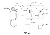
1つの態様において、例えば図1に示されるように、少なくとも1つの生体特徴の識別によってユーザを認証するためのシステムは、(近赤外線を含む)赤外線のピーク発光波長を有する電磁放射線104を放射することができる活性光源102を含むことができる。活性光源102は、電磁放射線104を放射するように配置され、ユーザ108の少なくとも1つの特徴106に作用する。システムは、さらに、ユーザ108の少なくとも1つの顔特徴106から反射された電磁放射線112を受光して検出するように活性光源に対して配置された赤外線捕捉画素を有する画像センサ110を含むことができる。いくつかの態様において、画像センサは、IR強化検出センサとすることができる。処理モジュール114は、画像センサ110に機能的に結合され、検出された電磁放射線からユーザ108の少なくとも1つの生体特徴106の電子表現を生成するように動作可能である。さらに、認証モジュール116は、処理モジュール114に機能的に結合され、電子表現を受信して、当該電子表現とユーザ108の少なくとも1つの生体特徴106の認証基準118と比較することにより、ユーザ108を認証するように動作可能である。ハウジング120は、いくつかの態様においてはシステムの様々な要素を支持するように想定されている。しかしながら、そのようなハウジングの物理的構成は、特定の要素がハウジング内に物理的に配置されているか否かとともに、限定するものと考えるべきではないことに留意されたい。
In one aspect, as shown, for example, in FIG. 1, a system for authenticating a user by identifying at least one biometric feature emits
いくつかの態様において、図2に示されるように、システムは、認証モジュール116に機能的に結合された認証インジケータ202を含むことができる。したがって、認証インジケータ202は、システムによってユーザ108が認証されたという通知を提供することができる。いくつかの態様において、インジケータは、装置がセキュアモードまたは非セキュアモードで動作しているときにユーザに通知することができる。多種多様な認証インジケータおよびインジケータ機能が想定され、そのような通知を提供する任意のインジケータは、本範囲内であると考えられる。インジケータの性質はまた、利用されるシステムまたは電子装置の物理的性質に応じて変化することができる。例えば、いくつかの態様において、インジケータは、LED、可聴信号などの専用のインジケータとすることができる。他の態様において、インジケータは、電子画面の変化若しくは変動、いくつかの態様においては認証済みユーザについてのそのようなメニューの他のセット、または、他の態様においてはセキュアモードを示すロック若しくはドル記号アイコンなどのシンボル若しくはアイコンの外観とすることができる。インジケータはまた、ドア、ゲート、または他の障壁の開放などの物体の物理的状態の変化を含むことができる。したがって、認証インジケータ202は、図2に示されるようにハウジング120内に配置されるかまたはシステムの主要要素に物理的にリンクされることができ、または、インジケータは、システム/ハウジングから離れて配置されて遠隔的に起動されることができる。図2およびそれ以降の図について、前の図(例えば図1)からのコールアウト項目番号は、これらの図面の説明から説明を組み込むことが意図されることに留意されたい。これらの場合において、項目は、再度記載または説明されてもされなくてもよく、これまでの説明は適切な範囲に適用される。
In some aspects, as shown in FIG. 2, the system can include an
他の態様において、図3に示されるように、システムは、さらに、活性光源102による電磁放射線の放射と画像センサ110によって反射された電磁放射線の捕捉を同期させるための、画像センサ110と活性光源102との間に機能的に結合された同期要素302を含むことができる。さらに、いくつかの態様において、同期は、システム内の他の要素、例えば画像センサプロセッサによって処理することができる。システムの信号対雑音比は、それゆえに、電磁放射線の放射と反射された電磁放射線の捕捉を整合させることによって改善することができる。いくつかの態様において、同期要素302は、活性光源102の放射デューティサイクルと画像センサ110の捕捉デューティサイクルとを独立して制御することができ、したがって放射に対する捕捉の調整を可能とする。例えば、活性光源からユーザまでの距離の変化に起因する反射された電磁放射線における可変遅延は、画像センサの捕捉ウィンドウのタイミングおよび/または幅を調整することによって補償されることができる。同期要素は、物理的な電子装置および回路、ソフトウェア、またはそれらの組み合わせを含むことができることが想定され、同期を容易とする。
In another aspect, as shown in FIG. 3, the system further includes an
他の態様において、セキュアリソースに対してユーザを認証するためのシステムが提供される。セキュアリソースは、装置自体、装置の特定の部分へのアクセス、データの収集、ウェブサイト、リモートサーバなどとすることができる。そのようなシステムは、ユーザを認証するために均等物を含む上述したような要素を含むことができる。図4に示されるように、そのようなシステムは、さらに、認証モジュール116に機能的に結合された許可モジュール402を含むことができる。許可モジュール402は、ユーザ108の認証が発生したことを検証し、認証に基づいてセキュアリソース404の少なくとも一部へのアクセスを可能とするように動作可能である。認証ユーザの許可は、認証された個人に応じてセキュアリソースへの異なるレベルのアクセスを許可することができる。換言すれば、異なるタイプのユーザは、認証後に異なる許可レベルを有することができる。例えば、セキュアリソースのユーザは、おそらく管理者と比較してセキュアリソースへの低いアクセスを有する必要がある。
In another aspect, a system for authenticating a user against a secure resource is provided. A secure resource can be the device itself, access to a specific part of the device, data collection, a website, a remote server, and so on. Such a system can include elements as described above including equivalents to authenticate a user. As shown in FIG. 4, such a system can further include an
セキュアリソース、許可モジュールおよび認証システムの相互作用および物理的関係は、システムおよびセキュアリソースの設計に応じて変化することができ、そのような変化は、本範囲内であると考えられる。図4を参照すると、例えば、許可モジュール402は、認証モジュール116から異なる位置に示されている。これは、いくつかの態様にあてはまることができるが、互いに近接して配置されるまたは例えばオンチップ集積などのさらに一体化されたモジュールが想定される。システムが電子装置内に配置される場合において、例えば、認証モジュールまたは許可モジュールのうちの少なくとも一方は、その内部に配置されることができる。他の態様において、認証モジュールまたは許可モジュールのうちの少なくとも一方は、セキュアリソース内に配置されることができる。他の態様において、セキュアリソースは、電子装置とは物理的に分離されておりかつ異なることができる一方で、他の態様において、セキュアリソースは、電子装置内に配置されることができる。この後者は、保護されたデータベースまたは装置上にローカルに記憶されている他の保護された情報のための場合であり得る。したがって、本開示は、システムの構成部品が物理的に一体に組み込まれることができるかまたは必要に応じてそれらを分離することができることを想定している。他の態様において、セキュアリソースは、リモートセキュアリソースへのゲートウェイとすることができる。リモートセキュアリソースの1つの例は、金融システムを含む。そのような場合、ユーザの権限は、ユーザが金融取引において検証されるのを可能とすることができる。リモートセキュアリソースの他の例は、固有の個人の生体シグネチャのデータベースを含む。そのような場合、ユーザは、個人の大規模なデータベースから識別された後、飛行機、建物、または旅行先などのリソースへのアクセスを与えられるまたは拒否されることができる。
The interaction and physical relationship of secure resources, authorization modules and authentication systems can vary depending on the design of the system and secure resources, and such changes are considered to be within this scope. Referring to FIG. 4, for example, the
集積度はまた、システムおよび/またはシステム要素の物理的設計に反映させることができる。様々な機能モジュールは、互いにおよび/またはシステムに関連する他の要素と様々な程度に一体化されることができる。1つの態様において、例えば、認証モジュールまたは許可モジュールのうちの少なくとも一方は、画像センサとともにモノリシックに一体化されることができる。いくつかの場合において、そのような一体化は、電子装置のCPUから分離することができる。1つの態様において、システムは、携帯電子装置に一体化されることができる。 The degree of integration can also be reflected in the physical design of the system and / or system elements. The various functional modules can be integrated to varying degrees with each other and / or other elements associated with the system. In one aspect, for example, at least one of the authentication module or the authorization module can be monolithically integrated with the image sensor. In some cases, such integration can be separated from the CPU of the electronic device. In one aspect, the system can be integrated into a portable electronic device.
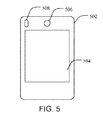
上述したように、本システムは、様々な方法で物理的構造に組み込まれることができる。1つの態様において、例えば、少なくとも活性光源、画像センサ、処理モジュール、および認証インジケータは、電子装置に一体化される。他の態様において、少なくとも活性光源、画像センサ、および処理モジュールは、電子装置に一体化される。システムは、認証/許可を提供するセキュアリソースおよび/または電子装置の性質に応じて変化するであろう多種多様な電子装置に一体化されることができることが想定される。そのような装置の非限定的例は、ハンドヘルド電子装置、携帯電子装置、携帯電話、スマートフォン、タブレットコンピュータ、パーソナルコンピュータ、現金自動預け払い機(ATM)、キオスク、クレジットカード端末、テレビ、ビデオゲームコンソールなどを含むことができ、必要に応じてそれらの組み合わせも含むことができる。図5は、スマートフォン502の非限定的例を示している。この場合、スマートフォン502は、その中に組み込まれた認証システムを含み、その大部分は図示していない。スマートフォンは、記載されているように、視覚的ディスプレイ504と、この場合には組み込まれた画像センサを有するカメオカメラ506とを含む。この場合、ユーザは、認証システムを起動することができ、視覚的ディスプレイ504にカメオカメラ506によって撮像されたユーザの顔の画像を並べることができ、システムによる認証を続行することができる。いくつかの態様において、認証インジケータ508は、装置がセキュアモードまたは非セキュアモードであるユーザに通知を提供するために装置に組み込むことができる。いくつかの態様において、そのような通知はまた、画面504によって提供されることができる。スマートフォンのカメオカメラがこの例において使用されているが、スマートフォンまたは任意の他の電子装置に関連付けられた非カメオカメラ/撮像装置が同様に利用可能であることに留意されたい。1つの態様において、生体認証またはジェスチャー認証に専用のカメオカメラおよび追加のカメラモジュールをスマートフォン上に含めることができる。さらに、いくつかの態様において、スタンドアローンのカメラは、インターネットまたはローカルネットワークシステムとともに、図5に示されるように装置またはシステムに一体化されることができる。いくつかの態様において、追加の生体カメラモジュールは、近赤外線波長の小範囲を除き、任意の光を除去する1つのフィルタまたは複数のフィルタを含むことができる。
As mentioned above, the system can be incorporated into the physical structure in various ways. In one aspect, for example, at least the active light source, the image sensor, the processing module, and the authentication indicator are integrated into the electronic device. In other embodiments, at least the active light source, the image sensor, and the processing module are integrated into the electronic device. It is envisioned that the system can be integrated into a wide variety of electronic devices that will vary depending on the nature of the secure resources and / or electronic devices that provide authentication / authorization. Non-limiting examples of such devices include handheld electronic devices, portable electronic devices, mobile phones, smartphones, tablet computers, personal computers, automated teller machines (ATMs), kiosks, credit card terminals, televisions, video game consoles. Etc., and combinations thereof as necessary. FIG. 5 shows a non-limiting example of the
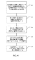
本開示は、さらに、セキュアリソースを使用するために電子装置によってユーザを許可するための方法を提供する。1つの態様において、図6に示されるように、例えば、そのような方法は、電子装置内の活性光源からユーザに対して約700nm〜約1200nmのピーク発光波長を有する電磁放射線を照射して、電磁放射線がユーザの少なくとも1つの生体特徴から反射させる工程602と、電子装置内に配置された画像センサで反射された電磁放射線を検出する工程604とを含む。ここで、画像センサは活性光源に対して配置された赤外線捕捉画素を含み、これにより、ユーザの少なくとも1つの生体特徴から反射された電磁放射線が受光および検出される。光捕捉画素は、複数の赤外電磁放射線の通過を容易とする構造配置を有する。本方法はまた、反射された電磁放射線からユーザの少なくとも1つの生体特徴の電子表現を生成する工程606と、ユーザの少なくとも1つの生体特徴の認証基準と電子表現を比較することによりユーザを認証ユーザとして認証する工程608と、認証されたユーザによるセキュアリソースの少なくとも一部の使用を許可する工程610とを含むことができる。他の態様において、本方法は、許可が成功して許可状態がアクティブであることの通知をユーザに提供する工程を含むことができる。さらに、いくつかの態様において、本方法は、セキュアリソースの使用中にユーザを定期的に認証する工程、または、他の態様においては、セキュアリソースの使用中にユーザを継続的に認証する工程を含むことができることが想定される。 The present disclosure further provides a method for authorizing a user by an electronic device to use secure resources. In one aspect, as shown in FIG. 6, for example, such a method includes irradiating a user with electromagnetic radiation having a peak emission wavelength of about 700 nm to about 1200 nm from an active light source in an electronic device, The step of reflecting 602 the electromagnetic radiation from at least one biometric feature of the user; and the step of detecting 604 the electromagnetic radiation reflected by an image sensor disposed within the electronic device. Here, the image sensor includes an infrared capture pixel disposed with respect to the active light source, whereby electromagnetic radiation reflected from at least one biological feature of the user is received and detected. The light capture pixel has a structural arrangement that facilitates passage of a plurality of infrared electromagnetic radiation. The method also generates 606 an electronic representation of at least one biometric feature of the user from the reflected electromagnetic radiation, and authenticates the user by comparing the electronic representation with an authentication criterion of the at least one biometric feature of the user. Authenticating as 608 and authorizing 610 the use of at least a portion of the secure resource by the authenticated user. In other aspects, the method can include providing a notification to the user that authorization is successful and the authorization state is active. Further, in some aspects, the method includes periodically authenticating the user during use of the secure resource, or in other aspects, continuously authenticating the user during use of the secure resource. It is envisioned that it can be included.
様々な活性光源が想定され、IR光を放射することができる任意の光源は、本範囲内であると考えられる。1つの態様において、例えば、活性光源は、約700nm〜約1200nmのピーク発光波長を有する電磁放射線を放射することができる。他の態様において、活性光源は、約900nmよりも大きいピーク発光波長を有する電磁放射線を放射することができる。さらに他の態様において、活性光源は、約850nm〜約1100nmのピーク発光波長を有する電磁放射線を放射することができる。さらなる態様において、活性光源は、約940nmのピーク発光を有する電磁放射線を放射することができる。太陽のスペクトルから入射する背景光量の低減のために940nm周囲の波長を有する光を利用することが特に有益である。940nmの光の波長は、大気中の水分によって太陽スペクトルからある程度はフィルタリングされる。そのため、この波長領域における背景ノイズは、周囲光が太陽光を含む場合には低減される。図7に示されるように、太陽のスペクトルがフィルタリングされた領域があり、背景スペクトル放射照度が940nmで低くなっている。約940nmで放射する活性光源を利用することにより、システムの信号対雑音比の向上、および認証の効率の向上が可能であり、また、電力を節約するために活性光源の強度を低減させることができ、屋外状況における機能性を向上させることができる。1つの特定の態様において、活性光源は、効果的な認証のために940nmにおいて少なくとも約0.1mW/cm2の強度を有する電磁放射線を生成することができる。 A variety of active light sources are envisioned and any light source capable of emitting IR light is considered within this range. In one aspect, for example, the active light source can emit electromagnetic radiation having a peak emission wavelength of about 700 nm to about 1200 nm. In other embodiments, the active light source can emit electromagnetic radiation having a peak emission wavelength greater than about 900 nm. In yet another aspect, the active light source can emit electromagnetic radiation having a peak emission wavelength of about 850 nm to about 1100 nm. In a further aspect, the active light source can emit electromagnetic radiation having a peak emission of about 940 nm. It is particularly beneficial to utilize light having a wavelength around 940 nm to reduce the amount of background light incident from the solar spectrum. The wavelength of light at 940 nm is filtered to some extent from the solar spectrum by atmospheric moisture. Therefore, background noise in this wavelength region is reduced when ambient light includes sunlight. As shown in FIG. 7, there is a region where the solar spectrum is filtered, and the background spectral irradiance is low at 940 nm. By utilizing an active light source that emits at about 940 nm, it is possible to improve the signal-to-noise ratio of the system and increase the efficiency of authentication, and to reduce the intensity of the active light source to save power. And the functionality in outdoor situations can be improved. In one particular aspect, the active light source can generate electromagnetic radiation having an intensity of at least about 0.1 mW / cm 2 at 940 nm for effective authentication.
活性光源は、使用される撮像および/または認証方法に応じて様々なモードで動作させることができる。例えば、活性光源は、連続的な態様、ストロボ発光の態様、ユーザ起動の態様、認証起動の態様、特定のパターン化された態様で、またはそれらの組み合わせなどで動作することができる。上述したように、活性光源は、撮像デューティサイクルに対応して間欠的に起動することができる。セキュアリソースへのアクセス中に連続的な認証が望まれる態様において、活性光源は、セキュアリソースへのアクセスを通して連続的に光を放射することができ、間欠的に光を放射することができるなどである。 The active light source can be operated in various modes depending on the imaging and / or authentication method used. For example, the active light source can operate in a continuous manner, a strobe mode, a user-activated mode, an authentication-activated mode, a specific patterned mode, or a combination thereof. As described above, the active light source can be activated intermittently in response to the imaging duty cycle. In an aspect where continuous authentication is desired during access to a secure resource, the active light source can emit light continuously through access to the secure resource, can emit light intermittently, etc. is there.
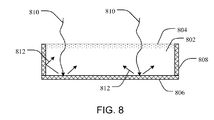
画像センサを参照すると、画像センサが組み込まれた装置の性質に応じてかつ様々なシステム設計パラメータに応じて構造および設計を変化させることができる。上述したように、画像センサは、複数の赤外電磁放射線の通過を容易とする構造配置を有する光捕捉画素を含むことができる。1つの例として、図8は、素子層802およびドープまたは接合領域804を有する画素を示している。画素は、さらに、ドープ領域804と対向する素子層802の側面に結合されたテクスチャ領域806を有して示されている。画素の任意の部分は、画像センサ設計に応じてテクスチャリングすることができる。図8はまた、側方光反射領域808を示し、さらなる光捕捉機能を実証する。光反射領域(808)は、テクスチャ領域、ミラー、ブラッグ反射器、充填されたトレンチ構造などであってよい。光810はまた、画素の素子層802と相互作用するように示されている。テクスチャ領域および反射領域(806または808のいずれか)は、812において示されるように、接触した際に素子層802に光を反射し返す。いくつかの態様において、806および/または808は、画像センサ装置内の画素を分離するためのトレンチ分離要素とすることができる。それゆえに、光は、画素によって捕捉され、反射光812が画素を通って戻るためにさらなる検出を容易とする。さらに、トレンチ分離要素は、画素内で光電子を捕捉することができ、画像センサにおけるクロストークの削減および高い変調伝達関数(modulation transfer function:MTF)を容易とする。テクスチャ領域との相互作用は、光の光路を増加させるために光を反射、散乱、拡散などさせることができることに留意されたい。これは、光を散乱することができる任意の要素によって達成することができる。他の態様において、ミラー、ブラッグ反射器などは、テクスチャ領域に加えてまたはその代わりに利用可能である。
Referring to the image sensor, the structure and design can be varied depending on the nature of the device in which the image sensor is incorporated and on various system design parameters. As described above, the image sensor can include light capture pixels having a structural arrangement that facilitates the passage of a plurality of infrared electromagnetic radiation. As one example, FIG. 8 shows a pixel having a
図9は、可視光および赤外光スペクトルの優れた信号対雑音比および高い量子効率を有する低光条件において動作可能である前面照射用画像センサ装置の1つの例示的な実施形態を示している。画像センサ装置900は、約10ミクロン未満の厚さを有する半導体素子層902と、接合を形成する少なくとも2つのドープ領域904、906と、入射する電磁放射線910と相互作用するように配置されたテクスチャ領域908とを含むことができる。他の態様において、半導体素子層902の厚さは、5ミクロン未満とすることができる。他の態様において、素子層の厚さは、7ミクロン未満とすることができる。さらに他の態様において、素子層の厚さは、2ミクロン未満とすることができる。素子層の厚さの下限は、装置の機能性を可能とする任意の厚さとすることができる。1つの態様において、しかしながら、素子層は、少なくとも10nmの厚さとすることができる。他の態様において、素子層は、少なくとも100nmの厚さとすることができる。さらに他の態様において、素子層は、少なくとも500nmの厚さとすることができる。
FIG. 9 illustrates one exemplary embodiment of a front-illuminated image sensor device that is operable in low light conditions with excellent signal to noise ratio and high quantum efficiency in the visible and infrared light spectrum. .
1つの態様において、そのような前面照射用画像センサは、900nmよりも大きい少なくとも1つの波長を有する電磁放射線について少なくとも約20%の外部量子効率を有することができる。他の態様において、画像センサは、900nmよりも大きい少なくとも1つの波長を有する電磁放射線について少なくとも約25%の外部量子効率を有することができる。他の態様において、そのような装置の外部量子効率は、900nmよりも大きい1つの波長について、少なくとも30%、少なくとも35%、または少なくとも40%とすることができる。記載された量子効率はまた、いくつかの態様においては約940nmの波長において達成することができることに留意されたい。他の態様において、850nmの波長がこれらの量子効率に利用可能である。 In one aspect, such a front-illuminated image sensor can have an external quantum efficiency of at least about 20% for electromagnetic radiation having at least one wavelength greater than 900 nm. In other aspects, the image sensor can have an external quantum efficiency of at least about 25% for electromagnetic radiation having at least one wavelength greater than 900 nm. In other aspects, the external quantum efficiency of such devices can be at least 30%, at least 35%, or at least 40% for one wavelength greater than 900 nm. Note that the described quantum efficiencies can also be achieved in some embodiments at a wavelength of about 940 nm. In other embodiments, a wavelength of 850 nm is available for these quantum efficiencies.
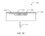
本開示の態様にかかる装置は、光学的に活性な半導体素子層と、回路層と、支持基板などを含むことができる。いくつかの態様において、半導体素子層は、シリコン素子層とすることができる。図10は、背面照射用の同様の画像センサを示している。画像センサ装置1000は、約10ミクロン未満の厚さを有する半導体素子層1002と、接合を形成する少なくとも2つのドープ領域1004、1006と、入射する電磁放射線1010と相互作用するように配置されたテクスチャ領域1008とを含むことができる。他の態様において、半導体素子層1002の厚さは、7ミクロン未満とすることができる。他の態様において、素子層の厚さは、5ミクロン未満とすることができる。さらに他の態様において、素子層の厚さは、2ミクロン未満とすることができる。素子層の厚さの下限は、装置の機能性を可能とする任意の厚さとすることができる。1つの態様において、しかしながら、素子層は、少なくとも10nmの厚さとすることができる。他の態様において、素子層は、少なくとも100nmの厚さとすることができる。さらに他の態様において、素子層は、少なくとも500nmの厚さとすることができる。
An apparatus according to aspects of the present disclosure can include an optically active semiconductor element layer, a circuit layer, a support substrate, and the like. In some aspects, the semiconductor device layer can be a silicon device layer. FIG. 10 shows a similar image sensor for backside illumination.
1つの態様において、そのような背面照射用画像センサは、900nmよりも大きい少なくとも1つの波長を有する電磁放射線について少なくとも約40%の外部量子効率を有することができる。他の態様において、画像センサは、900nmよりも大きい少なくとも1つの波長を有する電磁放射線について少なくとも約50%の外部量子効率を有することができる。他の態様において、そのような装置の外部量子効率は、900nmよりも大きい1つの波長について、少なくとも55%、少なくとも60%、または少なくとも65%とすることができる。記載された量子効率はまた、いくつかの態様においては約940nmの波長において達成することができることに留意されたい。 In one aspect, such a back-illuminated image sensor can have an external quantum efficiency of at least about 40% for electromagnetic radiation having at least one wavelength greater than 900 nm. In other aspects, the image sensor can have an external quantum efficiency of at least about 50% for electromagnetic radiation having at least one wavelength greater than 900 nm. In other aspects, the external quantum efficiency of such devices can be at least 55%, at least 60%, or at least 65% for one wavelength greater than 900 nm. Note that the described quantum efficiencies can also be achieved in some embodiments at a wavelength of about 940 nm.
多数の構成が想定され、任意の種類の接合構成は、本範囲内であると考えられる。例えば、第1および第2のドープ領域は、互いに異なることができ、互いに接触することができ、互いに重複することができるなどである。いくつかの場合において、固有領域は、第1および第2のドープ領域との間に少なくとも部分的に配置されることができる。さらに、いくつかの態様において、半導体素子層は、バルク半導体層または半導体支持層または絶縁層上の半導体上に配置されることができる。 A number of configurations are envisioned and any type of junction configuration is considered within the scope. For example, the first and second doped regions can be different from each other, can be in contact with each other, can overlap each other, and so forth. In some cases, the intrinsic region can be at least partially disposed between the first and second doped regions. Further, in some embodiments, the semiconductor element layer can be disposed on a semiconductor on a bulk semiconductor layer or a semiconductor support layer or an insulating layer.
テクスチャ領域は、半導体(例えばシリコン)材料の全面またはその一部のみに関連付けられることができることに留意されたい。さらに、いくつかの態様において、テクスチャ領域は、半導体材料の吸収経路長を最大化するように具体的には配置されることができる。他の態様において、第3のドープは、テクスチャ領域の近くに発生したキャリアの収集を改善するためにテクスチャ領域の近くに含めることができる。 Note that a texture region can be associated with the entire surface of a semiconductor (eg, silicon) material or only a portion thereof. Further, in some aspects, the texture region can be specifically arranged to maximize the absorption path length of the semiconductor material. In other aspects, a third dope can be included near the texture region to improve the collection of carriers generated near the texture region.
そのような感光性素子に関するさらなる詳細は、2011年6月20日付で出願された米国特許出願第13/164,630号に記載されており、この参照によりその全体が本明細書に組み込まれる。 Further details regarding such photosensitive elements are described in US patent application Ser. No. 13 / 164,630, filed Jun. 20, 2011, which is hereby incorporated by reference in its entirety.
さらに、前面照射または背面照明であるかにかかわらず、テクスチャ領域は、入射する電磁放射線の反対側の半導体素子層の側に配置することができる。テクスチャ領域はまた、入射する電磁放射線に隣接する半導体素子層の側に配置されることができる。換言すれば、この場合には、電磁放射線は、半導体素子層内を通過する前にテクスチャ領域に接触する。さらに、テクスチャ領域は、反対側および半導体素子層の隣接側の双方に配置されることができることが想定される。 Furthermore, whether it is front-illumination or back-illumination, the texture region can be located on the side of the semiconductor element layer opposite to the incident electromagnetic radiation. The texture region can also be located on the side of the semiconductor device layer adjacent to the incident electromagnetic radiation. In other words, in this case, the electromagnetic radiation contacts the texture region before passing through the semiconductor element layer. Further, it is envisioned that the texture region can be disposed on both the opposite side and the adjacent side of the semiconductor element layer.
画像センサを構築するために利用される半導体は、そのような画像センサが本明細書において記載された特性を有して構成されることができる任意の有用な半導体材料とすることができる。1つの態様において、しかしながら、半導体素子層はシリコンである。しかしながら、シリコン光検出器は、特に薄膜シリコン素子の場合、光のIR波長の検出可能性が制限されることに留意されたい。従来のシリコン素子は、約700nmよりも長い波長を有する光子を検出するためにかなりの吸収深さを必要とする。可視光は、最初の数ミクロンのシリコン層において容易に吸収されることができるが、薄いウェハ深さ(例えば、約20μm)におけるより長い波長(例えば、>900nm)のシリコンにおける吸収は不十分である。本画像センサ装置は、シリコンの薄層における電磁放射線の吸収を増加させることができる。 The semiconductor utilized to construct the image sensor can be any useful semiconductor material in which such an image sensor can be configured with the characteristics described herein. In one embodiment, however, the semiconductor device layer is silicon. However, it should be noted that silicon photodetectors are limited in their ability to detect the IR wavelength of light, particularly in the case of thin film silicon devices. Conventional silicon devices require a significant absorption depth to detect photons having wavelengths longer than about 700 nm. Visible light can be easily absorbed in the first few microns of silicon layer, but absorption in longer wavelength (eg,> 900 nm) silicon at thin wafer depths (eg, about 20 μm) is insufficient. is there. The image sensor device can increase the absorption of electromagnetic radiation in a thin layer of silicon.
テクスチャ領域は、特に近赤外線波長において、画像センサの吸収を増加させ、外部量子効率を向上させ、応答時間および遅延を低減させることができる。そのような固有かつ新規な装置は、高速シャッタ速度を可能とし、それによって低光シナリオにおける移動物体の撮像を可能とする。シリコンベース素子における増加した近赤外線感度は、活性光源において必要な電力を低減することができ、素子が正確な個人の生体測定値を捕捉することができる距離を増加させることができる。 Texture regions can increase absorption of the image sensor, improve external quantum efficiency, and reduce response time and delay, especially at near infrared wavelengths. Such a unique and novel device allows for a high shutter speed, thereby enabling imaging of moving objects in low light scenarios. Increased near-infrared sensitivity in silicon-based devices can reduce the power required in the active light source and can increase the distance that the device can capture accurate personal biometrics.
本システムは、装置と個人との間の撮像距離を増加させるための光学系を含むことができることが想定されるが、テクスチャ領域を有する画像センサ装置は、システムが比較的長距離においてさえも低いIR光強度レベルで機能するのを可能とする。これは、エネルギ消費と熱管理の問題を低減し、携帯装置のバッテリ寿命を増大させるともに、高強度IR光から生じることがある副作用を潜在的に減少させる。1つの態様において、例えば、画像センサ装置は、約700nm〜約1200nmの少なくとも1つの波長を有し、かつ約12インチ〜約24インチの距離で個人に作用する約5uW/cm2未満の背景放射照度を有する活性光源から放射された電磁放射線を使用して、実質的に固有の顔特徴を識別するために十分な詳細を有する個人の電子表現を撮像することができる。他の態様において、画像センサ装置は、約700nm〜約1200nmの少なくとも1つの波長を有し、かつ約18インチの距離で個人に作用する約5uW/cm2未満の背景放射照度を有する活性光源から放射された電磁放射線を使用して、実質的に固有の顔特徴を識別するために十分な詳細を有する個人の電子表現を撮像することができる。さらに他の態様において、画像センサ装置は、約800nm〜約1000nmの少なくとも1つの波長を有し、かつ約18インチの距離で個人に作用する約1uW/cm2〜約100uW/cm2の背景放射照度を有する活性光源から放射された電磁放射線を使用して、実質的に固有の顔特徴を識別するために十分な詳細を有する個人の電子表現を撮像することができる。さらに他の態様において、画像センサ装置は、約800nm〜約1000nmの少なくとも1つの波長を有しかつ約1uW/cm2〜約10uW/cm2である約18インチで個人に作用する背景放射照度を有する活性光源から放射された電磁放射線を使用して、実質的に固有の顔特徴を識別するために十分な詳細を有する個人の電子表現を撮像することができる。 While it is envisioned that the system can include an optical system to increase the imaging distance between the device and the individual, image sensor devices with textured regions are low even when the system is relatively long distance Allows functioning at IR light intensity levels. This reduces energy consumption and thermal management issues, increases the battery life of the portable device, and potentially reduces side effects that may arise from high intensity IR light. In one aspect, for example, the image sensor device has a background radiation of less than about 5 uW / cm 2 having at least one wavelength of about 700 nm to about 1200 nm and acting on an individual at a distance of about 12 inches to about 24 inches. Electromagnetic radiation emitted from an active light source with illumination can be used to image an electronic representation of an individual with sufficient detail to identify substantially unique facial features. In another aspect, the image sensor device is from an active light source having at least one wavelength of about 700 nm to about 1200 nm and having a background irradiance of less than about 5 uW / cm 2 acting on an individual at a distance of about 18 inches. The emitted electromagnetic radiation can be used to image an electronic representation of an individual with sufficient detail to identify substantially unique facial features. In yet another aspect, the image sensor device has a background radiation of about 1 uW / cm 2 to about 100 uW / cm 2 having at least one wavelength of about 800 nm to about 1000 nm and acting on an individual at a distance of about 18 inches. Electromagnetic radiation emitted from an active light source with illumination can be used to image an electronic representation of an individual with sufficient detail to identify substantially unique facial features. In yet another aspect, the image sensor device has a background irradiance acting on an individual at about 18 inches having at least one wavelength from about 800 nm to about 1000 nm and from about 1 uW / cm 2 to about 10 uW / cm 2. Electromagnetic radiation emitted from an active light source can be used to image an electronic representation of an individual with sufficient detail to identify substantially unique facial features.
上述したように、いくつかの態様において、素子のシリコン材料の厚さは、感度および応答時間を決定することができる。標準的なシリコン素子は、近赤外線スペクトルに入る波長を検出するために、厚く、すなわち50μmよりも大きくする必要があり、そのような厚い素子による検出は、応答の遅さおよび高い暗電流をもたらす。テクスチャ領域は、素子において赤外光の吸収を増加させるために電磁放射線と相互作用するように配置されており、それによって高速動作を可能としつつ赤外線感度を向上させる。拡散散乱や反射は、特に内部全反射と組み合わせた場合、吸収についての増加した経路長をもたらすことがあり、シリコン画素、光検出器、画素アレイ、画像センサなどについての赤外線における応答性の大きな改善をもたらす。吸収経路長の増加により、薄いシリコン材料を使用して、赤外線領域に電磁放射線を吸収することが可能となる。薄いシリコン材料素子の1つの利点は、電荷キャリアがより迅速に素子から掃引され、したがって応答時間を削減させるということである。逆に、厚いシリコン材料素子は、拡散によって少なくとも部分的に、よりゆっくりとそこから電荷キャリアを掃引する。 As described above, in some aspects, the thickness of the silicon material of the device can determine sensitivity and response time. Standard silicon devices need to be thick, ie, greater than 50 μm, to detect wavelengths that fall into the near-infrared spectrum, and detection with such thick devices results in slow response and high dark current . The texture region is arranged to interact with electromagnetic radiation to increase the absorption of infrared light in the device, thereby improving infrared sensitivity while allowing high speed operation. Diffuse scattering and reflection can result in increased path length for absorption, especially when combined with total internal reflection, greatly improving infrared responsiveness for silicon pixels, photodetectors, pixel arrays, image sensors, etc. Bring. The increase in absorption path length makes it possible to absorb electromagnetic radiation in the infrared region using a thin silicon material. One advantage of a thin silicon material device is that charge carriers are swept from the device more quickly, thus reducing response time. Conversely, thick silicon material elements sweep charge carriers therefrom more slowly, at least partially by diffusion.
しかしながら、半導体素子層は、電磁放射線の検出および変換機能を可能とする任意の厚さとすることができ、したがって任意のそのような半導体素子層の厚さは、本範囲内であると考えられることに留意されたい。上述したように、薄いシリコン層材料は、応答時間およびバルク暗電流発生を低減させる際に特に有益であり得る。上述したように、電荷キャリアは、より厚いシリコン材料層に比べて薄いシリコン材料層からより迅速に掃引することができる。薄いシリコン、少ない材料、電子/正孔は、収集されるために横断しなければならず、キャリアの集合を捕捉または遅らせることができる欠陥が発生した生成電荷キャリアの確率は低い。したがって、高速写真応答を実施する1つの目的は、画像センサの半導体素子層について薄いシリコン材料を利用することである。そのような素子は、画素の電位への構築および電界のドリフトによってキャリアを生成した写真の高速収集を提供するために任意に印加されるバイアスによって電荷キャリアをほぼ空乏化することができる。画素の非空乏領域内に残存する電荷キャリアは、ドリフト輸送より遅い拡散輸送によって収集される。このため、拡散が空乏ドリフト領域よりもはるかに薄くなるように支配することができる任意の領域の厚さを有することが望ましいことがある。他の態様において、シリコン材料は、内部バイアスが電荷キャリアの飽和速度について十分な電界を発生させるように厚さおよび基板ドープ濃度を有することができる。 However, the semiconductor element layer can be of any thickness that allows for the detection and conversion function of electromagnetic radiation, and therefore the thickness of any such semiconductor element layer is considered to be within this range. Please note that. As discussed above, thin silicon layer materials can be particularly beneficial in reducing response time and bulk dark current generation. As described above, charge carriers can be swept more quickly from a thin silicon material layer than from a thicker silicon material layer. Thin silicon, few materials, electrons / holes must be traversed in order to be collected, and the probability of generated charge carriers with defects that can trap or delay the collection of carriers is low. Thus, one purpose of implementing a high speed photographic response is to utilize a thin silicon material for the semiconductor element layer of the image sensor. Such devices can substantially deplete charge carriers with an arbitrarily applied bias to provide a fast collection of photographs that have generated carriers due to pixel potential buildup and field drift. Charge carriers remaining in the non-depleted region of the pixel are collected by diffusion transport that is slower than drift transport. For this reason, it may be desirable to have the thickness of any region where the diffusion can dominate to be much thinner than the depletion drift region. In other embodiments, the silicon material can have a thickness and substrate doping concentration such that the internal bias generates a sufficient electric field for the charge carrier saturation rate.
したがって、本開示の態様にかかる画像センサ装置は、とりわけ、所定のシリコン厚さについて光スペクトルの赤外光部分における高い量子効率を提供する。そのため、高い量子効率、低バルク暗電流生成、および応答時間または遅延の低減は、近赤外線における波長について得ることができる。換言すれば、感度はより高く、応答時間は、厚い素子においてみられるよりも速く、近赤外線における同様の量子効率を達成する。 Thus, an image sensor device according to aspects of the present disclosure provides high quantum efficiency in the infrared portion of the light spectrum, among other things, for a given silicon thickness. Thus, high quantum efficiency, low bulk dark current generation, and reduced response time or delay can be obtained for wavelengths in the near infrared. In other words, the sensitivity is higher and the response time is faster than seen in thicker devices, achieving the same quantum efficiency in the near infrared.
シリコンに加えて、他の半導体材料は、本開示の画像センサ装置における使用のために想定される。そのような半導体材料の非限定的例は、IV族材料、IIおよびVI族からの材料からなる化合物および合金、IIIおよびV族からの材料からなる化合物および合金、および、それらの組み合わせを含むことができる。より具体的には、典型的なIV族材料は、シリコン、炭素(例えばダイヤモンド)、ゲルマニウム、およびそれらの組み合わせを含むことができる。IV族材料の様々な例示的な組み合わせは、シリコンカーバイド(SiC)やシリコンゲルマニウム(SiGe)を含むことができる。典型的なシリコン材料は、例えば、アモルファスシリコン(a−Si)、微結晶シリコン、多結晶シリコン、および単結晶シリコンならびに他の結晶型を含むことができる。他の態様において、半導体材料は、シリコン、炭素、ゲルマニウム、窒化アルミニウム、窒化ガリウム、インジウムガリウム砒素、アルミニウムガリウム砒素、およびそれらの組み合わせのうちの少なくとも1つを含むことができる。 In addition to silicon, other semiconductor materials are envisioned for use in the image sensor device of the present disclosure. Non-limiting examples of such semiconductor materials include Group IV materials, compounds and alloys consisting of materials from Group II and VI, compounds and alloys consisting of materials from Group III and V, and combinations thereof Can do. More specifically, typical Group IV materials can include silicon, carbon (eg, diamond), germanium, and combinations thereof. Various exemplary combinations of Group IV materials can include silicon carbide (SiC) and silicon germanium (SiGe). Typical silicon materials can include, for example, amorphous silicon (a-Si), microcrystalline silicon, polycrystalline silicon, and single crystal silicon and other crystalline forms. In other aspects, the semiconductor material can include at least one of silicon, carbon, germanium, aluminum nitride, gallium nitride, indium gallium arsenide, aluminum gallium arsenide, and combinations thereof.
II〜VI族材料の典型的な組み合わせは、セレン化カドミウム(CdSe)、硫化カドミウム(CdS)、テルル化カドミウム(CdTe)、酸化亜鉛(ZnO)、セレン化亜鉛(ZnSe)、硫化亜鉛(ZnS)、テルル化亜鉛(ZnTe)、テルル化カドミウム亜鉛(CdZnTe、CZT)、テルル化水銀カドミウム(HgCdTe)、水銀テルル化亜鉛(HgZnTe)、水銀セレン化亜鉛(HgZnSe)、およびそれらの組み合わせを含むことができる。 Typical combinations of II-VI materials are cadmium selenide (CdSe), cadmium sulfide (CdS), cadmium telluride (CdTe), zinc oxide (ZnO), zinc selenide (ZnSe), zinc sulfide (ZnS). , Zinc telluride (ZnTe), cadmium zinc telluride (CdZnTe, CZT), mercury cadmium telluride (HgCdTe), mercury telluride (HgZnTe), mercury selenide (HgZnSe), and combinations thereof it can.
III〜V族材料の典型的な組み合わせは、アンチモン化アルミニウム(AlSb)、ヒ化アルミニウム(AlAs)、窒化アルミニウム(AlN)、リン化アルミニウム(AlP)、窒化ホウ素(BN)、リン化ホウ素(BP)、ホウ素砒素(BAs)、アンチモン化ガリウム(GaSb)、ガリウム砒素(GaAs)、窒化ガリウム(GaN)、ガリウムリン(GaP)、インジウムアンチモン(InSb)、インジウム砒素(InAs)、窒化インジウム(InN)、リン化インジウム(InP)、アルミニウムガリウム砒素(AlGaAs、AlxGa1−xAs)、インジウムガリウム砒素(InGaAs、InxGa1−xAs)、インジウムガリウムリン(InGaP)、アルミニウムインジウム砒素(AlInAs)、アルミニウムアンチモン化インジウム(AlInSb)、窒化ガリウム砒素(GaAsN)、ガリウム砒素リン(GaAsP)、窒化アルミニウムガリウム(AlGaN)、アルミニウムガリウムリン(AlGaP)、窒化インジウムガリウム(InGaN)、インジウム砒素アンチモン(InAsSb)、インジウムアンチモン化ガリウム(InGaSb)、アルミニウムガリウムインジウムリン(AlGaInP)、アルミニウムガリウム砒素リン(AlGaAsP)、インジウムガリウム砒素リン(InGaAsP)、アルミニウムインジウム砒素リン(AlInAsP)、窒化アルミニウムガリウム砒素(AlGaAsN)、窒化インジウムガリウム砒素(InGaAsN)、窒化インジウムアルミニウム砒素(InAlAsN)、窒化砒素ガリウムアンチモン(GaAsSbN)、窒化ガリウムインジウム砒素アンチモン(GaInNAsSb)、ガリウムインジウム砒素リンアンチモン(GaInAsSbP)、およびそれらの組み合わせを含むことができる。 Typical combinations of III-V materials are aluminum antimonide (AlSb), aluminum arsenide (AlAs), aluminum nitride (AlN), aluminum phosphide (AlP), boron nitride (BN), boron phosphide (BP ), Boron arsenide (BAs), gallium antimonide (GaSb), gallium arsenide (GaAs), gallium nitride (GaN), gallium phosphide (GaP), indium antimony (InSb), indium arsenide (InAs), indium nitride (InN) Indium phosphide (InP), aluminum gallium arsenide (AlGaAs, Al x Ga 1-x As), indium gallium arsenide (InGaAs, In x Ga 1-x As), indium gallium phosphide (InGaP), aluminum indium arsenide (AlInAs) ) Indium aluminum antimonide (AlInSb), gallium arsenide (GaAsN), gallium arsenide phosphorus (GaAsP), aluminum gallium nitride (AlGaN), aluminum gallium phosphide (AlGaP), indium gallium nitride (InGaN), indium arsenide antimony (InAsSb), Indium gallium antimonide (InGaSb), aluminum gallium indium phosphide (AlGaInP), aluminum gallium arsenide phosphorus (AlGaAsP), indium gallium arsenide phosphorus (InGaAsP), aluminum indium arsenide phosphorus (AlInAsP), aluminum gallium arsenide nitride (AlGaAsN), indium nitride Gallium arsenide (InGaAsN), indium aluminum arsenide nitride (InAlAsN), It may include gallium arsenide antimony nitride (GaAsSbN), gallium indium arsenide antimony (GaInNAsSb), gallium indium arsenide phosphide antimony (GaInAsSbP), and combinations thereof.
さらに、様々な種類の半導体材料が想定され、電磁放射線検出装置に組み込むことができる任意のそのような材料は、本範囲内であると考えられる。1つの態様において、例えば、半導体材料は単結晶である。他の態様において、半導体材料は多結晶である。さらに他の態様において、半導体材料は微結晶である。また、半導体材料は、アモルファスとすることができることが想定される。具体的な非限定例は、アモルファスシリコンやアモルファスセレンを含む。 Further, various types of semiconductor materials are envisioned and any such material that can be incorporated into an electromagnetic radiation detection device is considered within the scope. In one embodiment, for example, the semiconductor material is a single crystal. In other embodiments, the semiconductor material is polycrystalline. In yet another aspect, the semiconductor material is microcrystalline. It is also envisioned that the semiconductor material can be amorphous. Specific non-limiting examples include amorphous silicon and amorphous selenium.
本開示の半導体材料は、様々な製造プロセスを使用して作製することができる。いくつかの場合において、製造手順は、装置の効率に影響を与えることができ、所望の結果を達成するために考慮に入れることができる。典型的な製造プロセスは、チョクラルスキー(Cz)プロセス、磁気チョクラルスキー(mCz)プロセスフロートゾーン(FZ)プロセス、エピタキシャル成長、または蒸着プロセスなどを含むことができる。本発明において使用される半導体材料は、単結晶材料とその上に形成されたエピタキシャル成長層との組み合わせとすることができることが想定される。 The semiconductor materials of the present disclosure can be made using a variety of manufacturing processes. In some cases, the manufacturing procedure can affect the efficiency of the device and can be taken into account to achieve the desired result. Typical manufacturing processes can include a Czochralski (Cz) process, a magnetic Czochralski (mCz) process float zone (FZ) process, an epitaxial growth, or a deposition process. It is envisioned that the semiconductor material used in the present invention can be a combination of a single crystal material and an epitaxial growth layer formed thereon.
様々なドーパント材料は、画像センサ装置の複数のドープ領域、テクスチャ領域、または任意の他のドープ部を形成するために想定され、そのようなプロセスにおいて使用可能な任意のそのようなドーパントは、本範囲内であると考えられる。利用される特定のドーパントは、ドープされる材料および得られた材料の使用目的に応じて変化することができることに留意すべきである。当該技術分野において公知の任意のドーパントは、本開示の構造をドープするために利用可能であることに留意されたい。 Various dopant materials are envisioned to form multiple doped regions, texture regions, or any other doped portion of the image sensor device, and any such dopants that can be used in such processes are It is considered to be within range. It should be noted that the particular dopant utilized can vary depending on the material being doped and the intended use of the resulting material. It should be noted that any dopant known in the art can be used to dope the structure of the present disclosure.
したがって、第1のドープ領域および第2のドープ領域は、互いにおよび/または半導体素子層と比べて極性において領域がより正または負になることを引き起こすために電子供与または正孔供与種によってドープされることができる。1つの態様において、例えば、いずれかのドープ領域は、p−ドープされることができる。他の態様において、いずれかのドープ領域は、n−ドープされることができる。1つの態様において、例えば、p+およびn−ドーパントによってドープすることにより、第1のドープ領域は、極性を負とすることができ、第2のドープ領域は、極性を正とすることができる。いくつかの態様において、領域のn(−−)、n(−)、n(+)、n(++)、p(−−)、p(−)、p(+)、またはp(++)タイプのドープのバリエーションが使用可能である。さらに、いくつかの態様において、半導体材料は、第1および第2のドープ領域に加えてドープされることができる。半導体材料は、第1および第2のドープ領域のうちの1もしくはそれ以上とは異なるドープ極性を有するようにドープされることができ、または、半導体材料は、第1および第2のドープ領域のうちの1もしくはそれ以上と同じであるドープ極性を有するようにドープされることができる。1つの特定の態様において、半導体材料は、p−型であるようにドープされることができ、第1および第2のドープ領域のうちの1もしくはそれ以上は、n−型であるようにドープされることができる。他の特定の態様において、半導体材料は、n−型であるようにドープされることができ、第1および第2のドープ領域のうちの1もしくはそれ以上は、p−型であるようにドープされることができる。1つの態様において、第1または第2のドープ領域のうちの少なくとも1つは、約0.1μm2〜約32μm2の表面積を有する。 Thus, the first doped region and the second doped region are doped with electron donating or hole donating species to cause the regions to be more positive or negative in polarity relative to each other and / or the semiconductor device layer. Can. In one embodiment, for example, any doped region can be p-doped. In other embodiments, any doped region can be n-doped. In one aspect, for example by doping with p + and n-dopants, the first doped region can be negative in polarity and the second doped region can be positive in polarity. In some embodiments, n (-), n (-), n (+), n (++), p (-), p (-), p (+), or p (++) of the region Variations on the type of dope can be used. Further, in some aspects, the semiconductor material can be doped in addition to the first and second doped regions. The semiconductor material can be doped to have a doping polarity different from one or more of the first and second doped regions, or the semiconductor material can be in the first and second doped regions. It can be doped to have a doping polarity that is the same as one or more of them. In one particular embodiment, the semiconductor material can be doped to be p-type and one or more of the first and second doped regions are doped to be n-type. Can be done. In other particular embodiments, the semiconductor material can be doped to be n-type, and one or more of the first and second doped regions can be doped to be p-type. Can be done. In one embodiment, at least one of the first or second doped region has a surface area of about 0.1 [mu] m 2 ~ about 32 [mu] m 2.
上述したように、テクスチャ領域は、電磁放射線を拡散するように、電磁放射線をリダイレクトするように、および電磁放射線を吸収するように機能することができ、それゆえに装置のQEを増加させる。テクスチャ領域は、シリコン材料の有効光路長を増加させるために表面特徴を含むことができる。表面特徴は、円錐、ピラミッド、柱、突起、マイクロレンズ、量子ドット、反転特徴などとすることができる。特徴サイズ、寸法、材料の種類、ドーパントプロファイル、テクスチャ位置などの操作などの要因は、拡散領域が特定の波長について調整可能であるのを可能とすることができる。1つの態様において、装置を調整することは、特定の波長または波長範囲が吸収されるのを可能とすることができる。他の態様において、装置を調整することは、特定の波長または波長範囲がフィルタリングを介して減少または除去されるのを可能とすることができる。 As described above, the texture region can function to diffuse electromagnetic radiation, redirect electromagnetic radiation, and absorb electromagnetic radiation, thus increasing the QE of the device. The texture region can include surface features to increase the effective optical path length of the silicon material. The surface features can be cones, pyramids, pillars, protrusions, microlenses, quantum dots, inversion features, and the like. Factors such as feature size, dimensions, material type, dopant profile, texture position, etc. can allow the diffusion region to be tunable for a particular wavelength. In one aspect, tuning the device can allow a particular wavelength or wavelength range to be absorbed. In other aspects, tuning the device may allow specific wavelengths or wavelength ranges to be reduced or eliminated via filtering.
上述したように、本開示の態様にかかるテクスチャ領域は、シリコン材料に、特に長波長(すなわち、赤外線)において、装置内に入射する電磁放射線の複数の通過を体験させることができる。そのような内部反射は、半導体素子層の厚さよりも大きくするように有効光路長を増加させる。この光路長の増加は、基板の厚さを増加させることなく、装置の量子効率を増大させ、改善された信号対雑音比をもたらす。テクスチャ領域は、入射電磁放射線に最も近い表面と関連付けることができ、または、テクスチャ領域は、入射電磁放射線に対して反対側の表面と関連付けることができ、それにより、放射がテクスチャ領域に当たる前にシリコン材料を通過するのを可能とする。さらに、テクスチャ領域は、ドープされることができる。1つの態様において、テクスチャ領域は、装置の裏面にドープされた接触領域を提供するように半導体素子層と同一または類似のドープ極性にドープされることができる。他の態様において、テクスチャ領域は、表面電界によって表面を不動態化するように半導体基板と同極性に高濃度でドープされることができる。他の態様において、テクスチャ領域は、テクスチャ層と隣接する基板との界面にダイオード接合(または空乏領域)を形成するように半導体基板とは逆極性にドープされることができる。 As described above, textured areas according to aspects of the present disclosure can cause the silicon material to experience multiple passes of electromagnetic radiation incident into the device, particularly at longer wavelengths (ie, infrared). Such internal reflection increases the effective optical path length to be greater than the thickness of the semiconductor element layer. This increase in optical path length increases the quantum efficiency of the device without increasing the substrate thickness, resulting in an improved signal to noise ratio. The texture region can be associated with the surface closest to the incident electromagnetic radiation, or the texture region can be associated with the surface opposite to the incident electromagnetic radiation, so that the silicon is irradiated before the radiation strikes the texture region. Allows to pass through the material. Furthermore, the texture region can be doped. In one aspect, the textured region can be doped with the same or similar doping polarity as the semiconductor device layer to provide a doped contact region on the backside of the device. In other embodiments, the textured region can be heavily doped with the same polarity as the semiconductor substrate to passivate the surface by a surface electric field. In other embodiments, the texture region can be doped with a reverse polarity to the semiconductor substrate to form a diode junction (or depletion region) at the interface between the texture layer and the adjacent substrate.
テクスチャ領域は、レーザ、化学エッチング(例えば、異方性エッチング、等方性エッチング)、ナノインプリント、リソグラフィテクスチャリング、さらなる材料蒸着、反応性イオンエッチングなどを含む様々な技術によって形成されることができる。テクスチャ領域を製造する1つの有効な方法は、レーザ加工によるものである。そのようなレーザ加工は、半導体素子層の個別の位置が最小量の材料除去で所望の深さにテクスチャリングされるのを可能とする。テクスチャ領域を形成するためのレーザ加工の様々な技術が想定され、そのような領域を形成することができる任意の技術は、本範囲内であると考えるべきである。レーザ処置または加工は、とりわけ、強化した吸収特性および増大した電磁放射線の検出を可能とすることができる。 Texture regions can be formed by various techniques including laser, chemical etching (eg, anisotropic etching, isotropic etching), nanoimprinting, lithographic texturing, further material deposition, reactive ion etching, and the like. One effective method of producing texture regions is by laser machining. Such laser processing allows individual locations of the semiconductor device layer to be textured to the desired depth with a minimum amount of material removal. Various techniques of laser processing to form textured regions are envisioned, and any technique that can form such regions should be considered within this scope. Laser treatment or processing, among other things, can allow enhanced absorption properties and increased detection of electromagnetic radiation.
1つの態様において、例えば、シリコン材料の標的領域は、レーザ放射によって照射されることができ、テクスチャ領域を形成する。そのような処理の例は、米国特許第7,057,256号明細書、米国特許第7,354,792号明細書、および米国特許第7,442,629号明細書においてさらに詳細に記載されており、この参照によりその全体が本明細書に組み込まれる。簡単に言えば、シリコンなどの半導体材料の表面は、レーザ放射によって照射され、テクスチャまたは表面改質領域を形成する。そのようなレーザ加工は、ドーパント材料の有無にかかわらず発生することができる。ドーパントが使用されるこれらの態様において、レーザは、ドーパントキャリアを介してシリコン表面上に向けることができる。この方法において、ドーパントキャリアからのドーパントは、シリコン材料の標的領域に導入される。シリコン材料に組み込まれたそのような領域は、本開示の態様にかかる様々な利点を有することができる。例えば、標的領域は、典型的には、本明細書において説明したメカニズムにより、レーザ加工された領域の面積を増大させ、放射線吸収の確率を増加させるテクスチャ表面を有する。1つの態様において、そのような標的領域は、レーザテクスチャリングによって生成されたミクロンサイズおよび/またはナノサイズの表面特徴を含む実質的にテクスチャリングされた表面である。他の態様において、シリコン材料の表面への照射は、照射が半導体にドーパントを組み込むようにドーパントに対してレーザ放射を晒すことを含む。様々なドーパント材料が当該技術分野で公知であり、本明細書においてより詳細に説明される。また、いくつかの態様において、そのようなレーザ加工は、シリコン材料を実質的にドープしない環境(例えば、アルゴン雰囲気)において発生することができることが理解される。 In one aspect, for example, a target region of silicon material can be illuminated by laser radiation to form a textured region. Examples of such treatment are described in further detail in US Pat. No. 7,057,256, US Pat. No. 7,354,792, and US Pat. No. 7,442,629. Which is hereby incorporated by reference in its entirety. In brief, the surface of a semiconductor material such as silicon is irradiated by laser radiation to form a texture or surface modified region. Such laser processing can occur with or without dopant material. In those embodiments where a dopant is used, the laser can be directed onto the silicon surface via a dopant carrier. In this method, dopant from the dopant carrier is introduced into the target region of the silicon material. Such regions incorporated into the silicon material can have various advantages according to aspects of the present disclosure. For example, the target region typically has a textured surface that increases the area of the laser machined region and increases the probability of radiation absorption by the mechanisms described herein. In one embodiment, such a target region is a substantially textured surface that includes micron-sized and / or nano-sized surface features generated by laser texturing. In other embodiments, irradiating the surface of the silicon material includes exposing laser radiation to the dopant such that the irradiation incorporates the dopant into the semiconductor. Various dopant materials are known in the art and are described in more detail herein. It is also understood that in some aspects, such laser processing can occur in an environment that is substantially not doped with silicon material (eg, an argon atmosphere).
したがって、テクスチャ領域を形成するシリコン材料の表面は、レーザ加工によって化学的および/または構造的に変更され、いくつかの態様において、ナノ構造、ミクロ構造、および/または表面上にパターン化された領域として現れる表面特徴の形成ならびにドーパントが使用される場合には半導体材料へのそのようなドーパントの組み込みをもたらすことができる。いくつかの態様において、そのような特徴は、大きさが50nm〜20μmのオーダーとすることができ、電磁放射線の吸収に役立つことができる。他の態様において、そのような特徴は、サイズが200nm〜2umのオーダーとすることができる。換言すれば、テクスチャ表面は、シリコン材料によって吸収される入射放射線の確率を増加させることができる。 Thus, the surface of the silicon material that forms the textured regions is chemically and / or structurally altered by laser processing, and in some embodiments, nanostructures, microstructures, and / or regions patterned on the surface Formation of surface features appearing as well as incorporation of such dopants into the semiconductor material, if dopants are used. In some embodiments, such features can be on the order of 50 nm to 20 μm in size and can help absorb electromagnetic radiation. In other embodiments, such features can be on the order of 200 nm to 2 um in size. In other words, the textured surface can increase the probability of incident radiation absorbed by the silicon material.
他の態様において、テクスチャ領域および/または半導体材料の少なくとも一部は、不動態化表面電界を生成するためにドーパントによってドープされることができ、テクスチャ領域が入射する電磁放射線とは反対側の半導体素子層の側に配置されている態様において、不動態化表面電界は、いわゆる裏面電界である。裏面電界は、収集効率および速度を改善するために、装置の裏面から接合に向かって生成された電荷キャリアに反発するように機能することができる。裏面電界の存在はまた、装置のテクスチャ表面層からの暗電流の寄与を抑制するように作用する。いくつかの態様において、深いトレンチ分離などのトレンチの表面は、キャリアに反発するように不動態化されることができることに留意されたい。さらにまた、裏面電界は、いくつかの態様において、そのようなトレンチ内に形成されることができる。 In other embodiments, at least a portion of the texture region and / or semiconductor material can be doped with a dopant to generate a passivating surface electric field, and the semiconductor opposite the electromagnetic radiation upon which the texture region is incident. In the embodiment arranged on the element layer side, the passivating surface electric field is a so-called back surface electric field. The back surface electric field can function to repel charge carriers generated from the back surface of the device towards the junction to improve collection efficiency and speed. The presence of the back surface field also acts to suppress the dark current contribution from the textured surface layer of the device. Note that in some aspects, the surface of the trench, such as deep trench isolation, can be passivated to repel carriers. Furthermore, the back surface field can be formed in such a trench in some embodiments.
他の態様において、図11に示されるように、半導体素子層1102は、第1のドープ領域1104と、第2のドープ領域1106と、ドープされた領域とは反対面上にテクスチャ領域1108とを有することができる。反射防止層1110は、テクスチャ層1108とは反対面において半導体素子層1102に結合されることができる。いくつかの態様において、反射防止層1110は、テクスチャ領域(図示せず)のように半導体素子層1102と同じ側にあることができる。さらにまた、いくつかの態様において、レンズは、半導体素子層に光学的に結合され、半導体素子層に入射する電磁放射線の焦点を合わせるために配置されることができる。
In another aspect, as shown in FIG. 11, the
本開示の他の態様において、画素アレイは、画像センサ装置として提供される。そのようなアレイは、入射光面、半導体素子層における少なくとも2つの画素を有する半導体素子層を含むことができ、各画素は、接合を形成する第1のドープ領域および第2のドープ領域と、半導体素子層に結合され、電磁放射線と相互作用するように配置されたテクスチャ領域とを含む。テクスチャ領域は、単一のテクスチャ領域または複数のテクスチャ領域とすることができる。さらに、画素アレイは、100um未満の厚さと、約800nmよりも大きい少なくとも1つの波長を有する電磁放射線について少なくとも75%の外部量子効率とを有することができる。画素アレイは、画素数を有することができ、または、約320×240(QVGA)以上の画素解像度として一般に知られている。他の態様において、画素解像度は、1MP(メガピクセル)よりも大きい、5MPよりも大きい、15MPよりも大きい、さらに25MPよりも大きい640×480(VGA)である。 In another aspect of the present disclosure, the pixel array is provided as an image sensor device. Such an array can include a semiconductor element layer having an incident light surface, at least two pixels in the semiconductor element layer, each pixel having a first doped region and a second doped region forming a junction; A texture region coupled to the semiconductor element layer and arranged to interact with the electromagnetic radiation. The texture region can be a single texture region or multiple texture regions. In addition, the pixel array can have a thickness of less than 100 um and an external quantum efficiency of at least 75% for electromagnetic radiation having at least one wavelength greater than about 800 nm. A pixel array can have a number of pixels or is generally known as a pixel resolution of about 320 × 240 (QVGA) or higher. In another aspect, the pixel resolution is 640 × 480 (VGA) greater than 1 MP (megapixel), greater than 5 MP, greater than 15 MP, and even greater than 25 MP.
図12に示されるように、例えば、半導体素子層1202は、第1のドープ領域1206および第2のドープ領域1208をそれぞれ有する少なくとも2つの画素1204を含むことができる。テクスチャ領域1210は、電磁放射線と相互作用するように配置されることができる。図13は、画素毎に別個のテクスチャ領域を示している。いくつかの態様において、しかしながら、アレイ内の複数の画素の吸収経路長を増加させるために単一のテクスチャの領域が使用可能である。さらにまた、分離構造1212は、電気的および/または光学的に互いから画素を分離するために画素間に配置されることができる。他の態様において、画素アレイは、各画素または画素によって生成された信号を処理する電子回路に電子的に結合されることができる。
As shown in FIG. 12, for example, the
様々な画像センサ構成および要素が想定され、全てのそのようなものは、本範囲内であると考えるべきである。そのような要素の非限定的例は、キャリアウエハ、トランジスタ、電気的接点、反射防止層、誘電層、回路層、ビア、転送ゲート、赤外線フィルタ、カラーフィルタアレイ(color filter array:CFA)、赤外線カットフィルタ、分離特徴などを含むことができる。様々な画像センサ解像度もまた想定され、全てのそのようなものは、本範囲内であると考えるべきである。そのような解像度の非制限的サンプルは、いわゆるQVGA、SVGA、VGA、HD720、HD1080、4Kなどである。さらに、そのような装置は、2010年9月17日付で出願された米国特許出願第12/885,158号に開示されているように、光吸収特性および要素を有することができ、この参照によりその全体が組み込まれる。画像センサは、CMOS(相補型金属酸化膜半導体)画像センサまたはCCD(電荷結合素子)とすることができることがさらに理解される。 Various image sensor configurations and elements are envisioned and all such should be considered within the scope. Non-limiting examples of such elements include carrier wafers, transistors, electrical contacts, antireflection layers, dielectric layers, circuit layers, vias, transfer gates, infrared filters, color filter arrays (CFA), infrared Cut filters, separation features, etc. can be included. Various image sensor resolutions are also envisioned and all such should be considered within this scope. Non-limiting samples of such resolution are so-called QVGA, SVGA, VGA, HD720, HD1080, 4K, etc. In addition, such devices can have light absorbing properties and elements, as disclosed in US patent application Ser. No. 12 / 885,158, filed on Sep. 17, 2010, which reference is hereby made. The whole is incorporated. It is further understood that the image sensor can be a CMOS (complementary metal oxide semiconductor) image sensor or a CCD (charge coupled device).
画像センサ装置は、装置の所望の設計に応じて画素あたり多数のトランジスタを含むことができる。1つの態様において、例えば、画像センサ装置は、少なくとも3つのトランジスタを含むことができる。他の態様において、撮像装置は、4個、5個、または6個以上のトランジスタを有することができる。例えば、図13は、本開示の1つの態様にかかるグローバルシャッタ動作を可能とする6トランジスタ(6−T)アーキテクチャの例示的な概略図を示している。画像センサは、画素(PD)と、グローバルリセット(Global_RST)と、グローバル転送ゲート(Global_TX)と、記憶ノードと、転送ゲート(TX1)と、リセット(RST)と、ソースフォロア(SF)と、フローティングディフュージョン(FD)と、行選択トランジスタ(RS)と、電源(Vaapix)と、出力電圧(Vout)とを含むことができる。余分な転送ゲートおよび記憶ノードに起因して、相関二重サンプリング(CDS)が可能である。したがって、読み出しノイズは、一般的なCMOS 4T画素に一致させることができるはずである。 Image sensor devices can include multiple transistors per pixel depending on the desired design of the device. In one aspect, for example, the image sensor device can include at least three transistors. In other embodiments, the imaging device can have 4, 5, or 6 or more transistors. For example, FIG. 13 shows an exemplary schematic of a 6-transistor (6-T) architecture that enables global shutter operation according to one aspect of the present disclosure. The image sensor includes a pixel (PD), a global reset (Global_RST), a global transfer gate (Global_TX), a storage node, a transfer gate (TX1), a reset (RST), a source follower (SF), and a floating state. A diffusion (FD), a row selection transistor (RS), a power source (Vapix), and an output voltage (Vout) can be included. Correlated double sampling (CDS) is possible due to extra transfer gates and storage nodes. Therefore, the readout noise should be able to be matched with a general CMOS 4T pixel.
ロールシャッタは、本範囲内であると考えられるが、グローバルシャッタの使用は、本装置およびシステムにおいて使用するのに有益であり得る。例えば、図14a〜bは、IR感知画像センサ装置によって撮像された被写体の虹彩の画像を示している。図14aからわかるように、ロールシャッタを使用して撮像された虹彩の画像は、撮像中の移動に起因して若干歪んでいる。これらの歪みは、個人の識別に影響を及ぼすことがある。一方、図14bは、グローバルシャッタを使用して撮像された虹彩の画像を示しており、そのような歪みを示していない。グローバルシャッタは、正確に同時に全ての画素を電子的に活性化することによって動作し、同時に背景からの光を統合して同時に統合を停止することができる。これは、ロールシャッタの歪みをなくす。 Although roll shutters are considered to be within this range, the use of a global shutter can be beneficial for use in the present apparatus and system. For example, FIGS. 14a-b show iris images of a subject imaged by an IR sensitive image sensor device. As can be seen from FIG. 14a, the iris image captured using the roll shutter is slightly distorted due to movement during imaging. These distortions can affect individual identification. On the other hand, FIG. 14b shows an iris image taken using a global shutter and does not show such distortion. A global shutter operates by electronically activating all pixels precisely at the same time, and can simultaneously integrate light from the background and stop the integration at the same time. This eliminates roll shutter distortion.
本開示の他の態様において、生体認証システムは、3次元(three dimensional:3D)光検知画像センサを含むことができる。そのような3Dタイプの画像センサは、顔特徴、身体特徴、歩幅、または身体位置特徴、耳特徴など、識別のために個人の表面の詳細を撮像するのに有用である。そのような3Dシステムは、これに限定されるものではないが、飛行時間型(Time−of−Flight:TOF)、構造化光、立体光などを含む任意の適用可能な3D技術を含むことができる。例えば、TOFは、そのような3D撮像のために利用可能な深さ情報を提供するためのレーダやLIDAR(Light Detection and Ranging;光検出および測距)システムにおける使用のために開発された1つの技術である。TOFの基本原理は、物体に信号を送信して標的から返された信号の特性を測定することを含む。測定された特性は、光子が光源を離れてから通過した時間、すなわちTOFを判定するために使用される。標的までの距離は、TOFの半分と信号の速度との乗算によって導出される。 In another aspect of the present disclosure, the biometric authentication system can include a three-dimensional (3D) light-sensitive image sensor. Such 3D type image sensors are useful for imaging details of an individual's surface for identification, such as facial features, body features, stride or body location features, ear features, etc. Such 3D systems may include any applicable 3D technology including, but not limited to, Time-of-Flight (TOF), structured light, stereoscopic light, etc. it can. For example, TOF is one developed for use in radar and LIDAR (Light Detection and Ranging) systems to provide depth information available for such 3D imaging. Technology. The basic principle of TOF involves sending a signal to an object and measuring the characteristics of the signal returned from the target. The measured property is used to determine the time that the photon has passed since leaving the light source, ie, the TOF. The distance to the target is derived by multiplying half of the TOF by the signal speed.
図15は、空間的に分離された複数の表面を有する標的によるTOF測定を図示している。式(III)は、標的までの距離を測定するために使用されることができ、dは標的までの距離であり、cは光速である。 FIG. 15 illustrates TOF measurement with a target having a plurality of spatially separated surfaces. Equation (III) can be used to measure the distance to the target, where d is the distance to the target and c is the speed of light.

標的1504に対して移動する光源1502から放射された光が要する時間(例えば、TOF)を測定することにより、光源(例えば、発光ダイオード(light emitting diode:LED))と標的の表面との距離が導出されることができる。そのような画像センサについて、各画素が上記TOF測定を行うことができる場合には、標的の3D画像を得ることができる。高い光速に起因して標的が光源に比較的近いとき、距離測定はTOF法では困難となる。したがって、1つの態様において、TOF測定は、変調されたLEDの光パルスを利用し、放射された光と受光した光との間の位相遅延を測定することができる。位相遅延およびLEDのパルス幅に基づいて、TOFを導出することができる。そのため、TOFの概念は、個人の識別に使用される画像を撮像するために各画素からの深さ情報を取得するためにCMOSおよびCCDセンサの双方において利用可能である。
By measuring the time required for light emitted from the
1つの例として、強化された赤外線応答を有するTOF 3D画素などの3D画素は、深さ精度を向上させることができ、順次3次元スケールにおいて顔特徴を示すことができる。1つの態様において、TOF画像センサは、可視光を遮断するフィルタを有し、そのためIR光のみを検出することができる。他の例において、強化された赤外線応答を有するTOF 3D画素などの3D画素は、正確な距離計算を行うために必要な光量を低減することができる。1つの態様において、撮像アレイは、少なくとも1つの3D赤外線検出画素と、互いに対して一体に配置された少なくとも1つの可視光検出画素とを含むことができる。図16a〜cは、そのようなアレイの画素配列の非限定的な構成例を示している。図16aは、赤色画素1602と青色画素1604と緑色画素1606とを有する画素アレイ構成の例を示している。さらに、光スペクトルのIR領域における強化された応答性または検出性を有する2つの3D TOF画素1608が含まれる。2つの3D画素の組み合わせは、より良好な深さ知覚を可能とする。図16bにおいて、示された画素配列は、図16aに記載された画像センサと、赤色画素、青色画素、および2つの緑色画素の3つのアレイとを含む。基本的に、1つのTOF画素は、RGGBの画素設計の第1象限を置き換える。この構成において、いくつかの緑色画素の追加は、同時に深さ知覚のために赤外光を捕捉しながら、人間の目にとっての緑色感度のニーズのために必要とされるより多くの緑色波長の捕捉を可能とする。本範囲は、画素アレイの数や配置によって限定されるべきではなく、任意の数および/または配置は、本範囲に含まれることに留意すべきである。図16cは、さらに他の態様にかかる画素の他の配置を示している。
As one example, 3D pixels, such as TOF 3D pixels with enhanced infrared response, can improve depth accuracy and can sequentially show facial features on a three-dimensional scale. In one aspect, the TOF image sensor has a filter that blocks visible light so that only IR light can be detected. In another example, a 3D pixel, such as a TOF 3D pixel with enhanced infrared response, can reduce the amount of light needed to perform an accurate distance calculation. In one aspect, the imaging array can include at least one 3D infrared detection pixel and at least one visible light detection pixel disposed integrally with respect to each other. Figures 16a-c show non-limiting configuration examples of pixel arrays of such arrays. FIG. 16 a shows an example of a pixel array configuration having
いくつかの態様において、TOF画素は、オンピクセルの光学的狭帯域通過フィルタを有することができる。狭帯域通過フィルタの設計は、変調された光源(LEDまたはレーザのいずれか)の発光スペクトルと一致させることができ、不要な周囲光を大幅に低減することができ、変調されたIR光の信号対雑音比をさらに向上させることができる。増加した赤外線QEの他の利点は、高速3D撮像のための高フレームレート動作の可能性である。統合されたIRカットフィルタは、忠実度の高いカラーレンダリングによって高品質の可視画像を可能とすることができる。センサチップ上に赤外線カットフィルタを統合することはまた、(典型的なIRフィルタガラスの除去に起因して)カメラモジュールの全体システムのコストを削減し、(携帯アプリケーションにとって良好な)モジュールプロファイルを削減することができる。これは、TOF画素および非TOF画素を利用することができる。 In some aspects, the TOF pixel may have an on-pixel optical narrow bandpass filter. Narrow bandpass filter design can match the emission spectrum of the modulated light source (either LED or laser), can significantly reduce unwanted ambient light, and modulate IR light signal The noise-to-noise ratio can be further improved. Another advantage of increased infrared QE is the possibility of high frame rate operation for high speed 3D imaging. The integrated IR cut filter can enable high quality visible images with high fidelity color rendering. Integrating an infrared cut filter on the sensor chip also reduces the overall system cost of the camera module (due to typical IR filter glass removal) and reduces the module profile (good for mobile applications) can do. This can utilize TOF pixels and non-TOF pixels.
図17は、本開示の1つの態様にかかる3次元TOF画素の例示的な概略図を示している。3D TOF画素は、標的の深さ測定を達成するために11個のトランジスタを有することができる。本実施形態において、3D画素は、画素(PD)と、グローバルリセット(Global_RST)と、第1のグローバル転送ゲート(Global_TX1)と、第1の記憶ノードと、第1の転送ゲート(TX1)と、第1のリセット(RST1)と、第1のソースフォロワ(SF1)と、第1のフローティングディフュージョン(FD1)と、第1の行選択トランジスタ(RS1)と、第2のグローバル転送ゲート(Global_TX2)と、第2の記憶ノードと、第2のトランスファゲート(TX2)と、第2のリセット(RST2)と、第2のソースフォロア(SF2)と、第2のフローティングディフュージョン(FD2)と、第2の行選択トランジスタ(RS2)と、電源(Vaapix)と、出力電圧(Vout)とを含むことができる。他のトランジスタは、3Dアーキテクチャに含めることができ、本発明の範囲内で考慮されるべきである。11個のトランジスタを有する特定の実施形態は、グローバルシャッタ動作に起因するモーションアーチファクトを低減することができ、それによってより正確な測定値を与える。 FIG. 17 shows an exemplary schematic of a three-dimensional TOF pixel according to one aspect of the present disclosure. A 3D TOF pixel can have 11 transistors to achieve target depth measurement. In this embodiment, the 3D pixel includes a pixel (PD), a global reset (Global_RST), a first global transfer gate (Global_TX1), a first storage node, and a first transfer gate (TX1). A first reset (RST1), a first source follower (SF1), a first floating diffusion (FD1), a first row selection transistor (RS1), a second global transfer gate (Global_TX2), A second storage node, a second transfer gate (TX2), a second reset (RST2), a second source follower (SF2), a second floating diffusion (FD2), a second Includes a row selection transistor (RS2), a power supply (Vapix), and an output voltage (Vout) Door can be. Other transistors can be included in the 3D architecture and should be considered within the scope of the present invention. Certain embodiments with eleven transistors can reduce motion artifacts due to global shutter operation, thereby providing more accurate measurements.
特にIRおよび可視光の双方が検出される場合に有益であり得る画素アレイ構造の他の例として、IRフィルタは、固有の画素アレイを生成するために可視光フィルタと統合することができる。例えば、従来のベイヤアレイは、2つの緑色、1つの赤色、および1つの青色の選択的画素を含む。より大きいアレイパターンは、散在するIR画素選択フィルタリングが強化された画像センサ機能を達成するのを同時に可能としながら、選択のおおよその比率を維持することに利用可能である。これは、可視域からIRまでの範囲の光を検出することができる画素を含む本開示の態様にかかる画像センサのために特に有用である。例えば、1つの態様において、本開示の態様にかかる画像センサは、約400nm〜約1200nmの波長を有する光を検出することができる。したがって、IR範囲における検出能に加えて、そのようなシリコン画像センサはまた、約400nm〜約700nmの可視領域の光に対して選択的である。したがって、そのような画素のアレイに対する様々なフィルタリング装置を機能的に結合することにより、緑色領域、青色領域、赤色領域、およびIR領域における選択的な検出が達成されることができる。フィルタはまた、入射する電磁放射線の経路の内外に移動可能に構成されることができることに留意されたい。 As another example of a pixel array structure that may be particularly beneficial when both IR and visible light are detected, an IR filter can be integrated with the visible light filter to produce a unique pixel array. For example, a conventional Bayer array includes two green, one red, and one blue selective pixels. Larger array patterns can be used to maintain an approximate ratio of selection while simultaneously allowing scattered IR pixel selection filtering to achieve enhanced image sensor functionality. This is particularly useful for image sensors according to aspects of the present disclosure that include pixels that can detect light in the visible to IR range. For example, in one aspect, an image sensor according to aspects of the present disclosure can detect light having a wavelength of about 400 nm to about 1200 nm. Thus, in addition to detectability in the IR range, such silicon image sensors are also selective for light in the visible region from about 400 nm to about 700 nm. Thus, by functionally combining various filtering devices for such an array of pixels, selective detection in the green, blue, red, and IR regions can be achieved. It should be noted that the filter can also be configured to be movable in and out of the path of incident electromagnetic radiation.
1つの態様において、例えば、複数のフィルタは、ベイヤーパターンで配置されることができ、約400nm〜約700nmの範囲の波長ならびに850nmよりも長い波長を有する所定の電磁放射線を通過させるように構成されることができる。他の態様において、可視電磁放射線は、約400nm〜約700nmの波長を含むことができ、赤外電磁放射線は、約900nmよりも大きい、いくつかの場合には約940nmである少なくとも1つの波長を含むことができる。 In one aspect, for example, the plurality of filters can be arranged in a Bayer pattern and configured to pass predetermined electromagnetic radiation having a wavelength in the range of about 400 nm to about 700 nm as well as a wavelength longer than 850 nm. Can. In other embodiments, the visible electromagnetic radiation can include a wavelength of about 400 nm to about 700 nm, and the infrared electromagnetic radiation has at least one wavelength that is greater than about 900 nm, in some cases about 940 nm. Can be included.
画素アレイの具体的なパターンは、装置の所望の特性に応じて変えることができる。1つの態様において、例えば、ベイヤーパターンは、IR選択画素によって1もしくはそれ以上の可視光選択画素を置き換えるためにフィルタを使用して変更することができる。緑色、赤色、または青色の画素のいずれかが、画素アレイ上にIR光を検出するように変更されることができる。1つの例として、アレイの緑色選択性を維持することは、2つの緑色通過画素フィルタ、1つの赤外線通過画素フィルタ、および1つの青色通過画素フィルタを含む複数の第1の2×2フィルタと、2つの緑色通過画素フィルタ、1つの赤外線通過画素フィルタ、および1つの赤色通過画素フィルタを含む複数の第1の2×2フィルタとを使用することによって達成することができる。そして、これらの2×2フィルタは、アレイにわたって均一な青色/赤色選択パターンを提供するために変えることができる。1つの例示的な実装が図18に示されている。さらに、緑色画素のいずれかは、同様にIR選択画素機能によって置き換えられることができることに留意されたい。 The specific pattern of the pixel array can vary depending on the desired characteristics of the device. In one aspect, for example, the Bayer pattern can be modified using a filter to replace one or more visible light selection pixels by IR selection pixels. Any of the green, red, or blue pixels can be modified to detect IR light on the pixel array. As one example, maintaining the green selectivity of the array includes a plurality of first 2 × 2 filters including two green pass pixel filters, one infrared pass pixel filter, and one blue pass pixel filter; This can be achieved by using a plurality of first 2 × 2 filters including two green pass pixel filters, one infrared pass pixel filter, and one red pass pixel filter. These 2 × 2 filters can then be varied to provide a uniform blue / red selection pattern across the array. One exemplary implementation is shown in FIG. Furthermore, it should be noted that any of the green pixels can be replaced by the IR selection pixel function as well.
さらに、電磁放射線は、複数または単一のフィルタを使用して可視範囲およびIR範囲の通過を可能とするようにフィルタリングすることができることもまた想定される。例えば、光は、900nmを上回る少なくとも1つの波長を有する可視光およびIR光の通過を可能とするようにフィルタリングされることができる。これらの範囲間にノッチフィルタを設けることにより、信号対雑音比を向上させることができる。さらにまた、活性光源の発光波長を中心とする狭帯域通過フィルタは、画像センサの効率をさらに向上させることができる。そのようなフィルタの1つの例は、可視光が930nmを上回るIR光とともに通過するのを可能とするが、約700nmと約930nmとの間の波長を有する光をフィルタリングするダイクロイックカットフィルタである。 It is further envisioned that electromagnetic radiation can be filtered using multiple or single filters to allow passage through the visible and IR ranges. For example, the light can be filtered to allow the passage of visible and IR light having at least one wavelength above 900 nm. By providing a notch filter between these ranges, the signal-to-noise ratio can be improved. Furthermore, the narrow band pass filter centered on the emission wavelength of the active light source can further improve the efficiency of the image sensor. One example of such a filter is a dichroic cut filter that allows visible light to pass with IR light above 930 nm, but filters light having a wavelength between about 700 nm and about 930 nm.
さらにまた、狭帯域IRフィルタは、得られる画像のさらなる処理を容易とすることができる。例えば、短い積分時間と組み合わせて狭帯域IRフィルタを使用することにより、可視画像は、改善されたIR画像を生成するためにIRフィルタリングされた画像から減算されることができる。結果として得られる画像はまた、オフセット減算に使用するために可視フレームを平均することにより、IRフレームが続き、再度可視フレームが続く可視フレームによる相関二重サンプリングを使用して処理されることができる。 Furthermore, the narrowband IR filter can facilitate further processing of the resulting image. For example, by using a narrowband IR filter in combination with a short integration time, the visible image can be subtracted from the IR filtered image to produce an improved IR image. The resulting image can also be processed using correlated double sampling with a visible frame followed by an IR frame by averaging the visible frames for use in offset subtraction. .
上述したように、個人を識別するためのシステムは、IR光を放射することが可能であるパッシブ光源(例えば、日光、周囲の室内灯)または活性光源(例えば、LEDまたは電球)のいずれかである光源を含むことができる。システムは、個人を識別するために有益に使用することができる任意の光源を利用することができる。そのため、1つの態様において、光源は、活性光源である。活性光源は、当該技術分野において周知であり、特にIRスペクトルにおける光を放射可能である。そのような活性光源は、連続的またはパルス状とすることができ、パルスは、撮像素子における光捕捉と同期されることができる。様々な光波長が放射され、個人を識別するために利用されるが、約700nm〜約1200nmの範囲のIR光が特に有用であり得る。さらに、いくつかの態様において、活性光源は、異なるピーク発光波長で赤外電磁放射線をそれぞれ放射する2若しくはそれ以上の活性光源とすることができる。IR範囲内の任意の異なる波長の発光が利用可能であり、非限定的例は、850nm、940nm、1064nmなどを含む。いくつかの態様において、2若しくはそれ以上の活性光源は、同時にまたはオフセットデューティサイクルで同じ画像センサ装置と相互作用することができる。そのような構成は、冗長な識別のために個人の1もしくはそれ以上の固有な特徴の独立した捕捉のために有用であり得る。この冗長な識別は、個人の正確な認証または識別を保証することができる。他の態様において、2若しくはそれ以上の活性光源は、異なる画像センサ装置とそれぞれ相互作用することができる。他の態様において、装置は、周囲光が識別を行うのに十分であるかどうかを判定することができ、それにより、活性光源を使用しないことによってバッテリ寿命を節約する。強化された赤外線量子効率を有する画像センサは、周囲光が受動的測定のために十分である可能性を増加させる。 As mentioned above, systems for identifying individuals are either passive light sources (eg, sunlight, ambient room lights) or active light sources (eg, LEDs or bulbs) that are capable of emitting IR light. A light source can be included. The system can utilize any light source that can be beneficially used to identify an individual. Thus, in one aspect, the light source is an active light source. Active light sources are well known in the art and are particularly capable of emitting light in the IR spectrum. Such an active light source can be continuous or pulsed, and the pulses can be synchronized with light capture at the imaging device. Various light wavelengths are emitted and utilized to identify individuals, but IR light in the range of about 700 nm to about 1200 nm can be particularly useful. Further, in some embodiments, the active light source can be two or more active light sources that each emit infrared electromagnetic radiation at different peak emission wavelengths. Any different wavelength emission within the IR range can be used, non-limiting examples include 850 nm, 940 nm, 1064 nm, and the like. In some embodiments, two or more active light sources can interact with the same image sensor device simultaneously or with an offset duty cycle. Such a configuration may be useful for independent capture of one or more unique features of an individual for redundant identification. This redundant identification can ensure accurate authentication or identification of the individual. In other embodiments, two or more active light sources can each interact with different image sensor devices. In other aspects, the device can determine whether ambient light is sufficient to make an identification, thereby saving battery life by not using an active light source. An image sensor with enhanced infrared quantum efficiency increases the likelihood that ambient light is sufficient for passive measurements.
上述したように、システムは、個人の識別を容易とするために、公知および認証された生体特徴と少なくとも1つの生体特徴を比較するように画像センサ装置に機能的に結合された分析モジュールを含むことができる。例えば、分析モジュールは、データベースなどのソースから個人の身元に関する既知のデータを取得し、この既知のデータを画像センサ装置によって捕捉されている電子表現と比較することができる。生体境界/測定値を定義して固有のコードに生体測定値を変換するために画像を分析することができる様々なアルゴリズムが知られている。そして、固有のコードは、個人の積極的な識別を行うための比較のために使用されるデータベースに記憶されることができる。そのようなアルゴリズムは、米国特許第4,641,349号明細書および米国特許第5,291,560号明細書において虹彩検出のために記載されており、この参照によりその全体が組み込まれる。画像処理モジュールおよび分析モジュールは、同じまたは異なるモジュールとすることができることに留意すべきである。本明細書において記載されたシステムは識別アルゴリズムのいずれかで利用可能であることが理解される。 As described above, the system includes an analysis module operably coupled to the image sensor device to compare at least one biometric feature with a known and authenticated biometric feature to facilitate personal identification. be able to. For example, the analysis module can obtain known data about an individual's identity from a source such as a database and compare this known data to an electronic representation captured by the image sensor device. Various algorithms are known that can analyze an image to define a biometric boundary / measurement value and convert the biometric value to a unique code. The unique code can then be stored in a database that is used for comparison to provide positive identification of individuals. Such an algorithm is described for iris detection in US Pat. No. 4,641,349 and US Pat. No. 5,291,560, which is incorporated by reference in its entirety. It should be noted that the image processing module and the analysis module can be the same or different modules. It is understood that the system described herein can be used with any of the identification algorithms.
さらにまた、様々な態様において、本システムは、様々な用途に適合するようなサイズにすることができることに留意されたい。これは、IR光に対する画像センサ装置の向上した感度およびIR放射の強度の対応する減少によってさらに容易とされ、それゆえに、光源のサイズまたは光源数の削減を可能とする。1つの態様において、例えば、光源、画像センサ装置、および画像処理モジュールは、まとめて約250立方ミリメートル未満のサイズを有する。1つの態様において、例えば、光源、画像センサ装置、および画像処理モジュールは、まとめて約160立方ミリメートル未満のサイズを有する。1つの態様において、例えば、画像センサ装置、レンズシステム、および画像処理モジュールは、まとめて約130立方ミリメートル未満のサイズを有する。1つの態様において、例えば、画像センサは、これに限定されるものではないが、レンズおよびフォーカス素子を含むカメラモジュールに組み込まれ、前記モジュールは、入射する電磁放射線の方向において6mm未満の厚さである。さらに他の態様において、光源、画像センサ装置、および画像処理モジュールは、まとめて約16立方センチメートル未満のサイズを有する。1つの態様において、画像センサ装置は、約1インチの光学フォーマットを有することができる。1つの態様において、画像センサ装置は、約1/2インチの光学フォーマットを有することができる。1つの態様において、画像センサ装置は、約1/3インチの光学フォーマットを有することができる。1つの態様において、画像センサ装置は、約1/4インチの光学フォーマットを有することができる。1つの態様において、画像センサ装置は、約1/7インチの光学フォーマットを有することができる。さらに他の態様において、画像センサ装置は、約1/10インチの光学フォーマットを有することができる。 Furthermore, it should be noted that in various aspects, the system can be sized to fit various applications. This is further facilitated by the improved sensitivity of the image sensor device to IR light and a corresponding decrease in the intensity of IR radiation, thus allowing a reduction in the size or number of light sources. In one aspect, for example, the light source, the image sensor device, and the image processing module collectively have a size of less than about 250 cubic millimeters. In one aspect, for example, the light source, the image sensor device, and the image processing module collectively have a size of less than about 160 cubic millimeters. In one aspect, for example, the image sensor device, the lens system, and the image processing module collectively have a size of less than about 130 cubic millimeters. In one aspect, for example, the image sensor is incorporated into a camera module that includes, but is not limited to, a lens and a focus element, said module having a thickness of less than 6 mm in the direction of incident electromagnetic radiation. is there. In yet another aspect, the light source, the image sensor device, and the image processing module collectively have a size of less than about 16 cubic centimeters. In one aspect, the image sensor device can have an optical format of about 1 inch. In one aspect, the image sensor device can have an optical format of about ½ inch. In one aspect, the image sensor device can have an optical format of about 1/3 inch. In one aspect, the image sensor device can have an optical format of about 1/4 inch. In one aspect, the image sensor device can have an optical format of about 1/7 inch. In yet another aspect, the image sensor device can have an optical format of about 1/10 inch.
他の態様において、識別システムは、電子装置に一体化されることができる。そのような装置の非限定的例は、携帯スマートフォン、携帯電話、ラップトップコンピュータ、デスクトップコンピュータ、タブレットコンピュータ、ATMs、テレビ、ビデオゲームコンソールなどを含むことができる。1つの特定の態様において、個人の積極的な識別は、電子装置のロックを解除するように動作可能である。この例において、電子装置は、ストレージレジストリに暗号化された許可ユーザの顔や虹彩識別特性を記憶し、個人の識別特性は、電子装置に組み込まれた認証システムによって捕捉される。認証システムは、積極的な識別のために記憶されている許可ユーザの識別特性と個人の識別特性とを比較することができる。この態様は、金融や法律上の取引または識別および/またはシグネチャを必要とする他の取引において個人を検証するために有益である。本明細書においては、ATM金融取引は、ユーザ認証システムを含むことができることが想定され、ここで、暗号化された許可ユーザの識別特性は、ATM装置が積極的な識別のためにカードに記憶されている許可ユーザの特性と個人の識別特性とを比較することができるようにATMのデビットカードに記憶されている。同様のシステムは、クレジットカードまたは商取引の他の項目に利用可能である。 In other aspects, the identification system can be integrated into an electronic device. Non-limiting examples of such devices can include mobile smart phones, mobile phones, laptop computers, desktop computers, tablet computers, ATMs, televisions, video game consoles, and the like. In one particular aspect, the positive identification of the individual is operable to unlock the electronic device. In this example, the electronic device stores the encrypted authorized user's face and iris identification characteristics in a storage registry, and the personal identification characteristics are captured by an authentication system embedded in the electronic device. The authentication system can compare the identification characteristics of authorized users stored for positive identification with the identification characteristics of individuals. This aspect is useful for verifying individuals in financial and legal transactions or other transactions that require identification and / or signatures. In this specification, it is envisaged that an ATM financial transaction can include a user authentication system, wherein the encrypted authorized user identification characteristics are stored on the card for positive identification by the ATM device. It is stored in the ATM debit card so that the characteristics of authorized users and personal identification characteristics can be compared. Similar systems are available for credit cards or other items of commerce.
他の例において、金融取引は、携帯電話装置を介して達成することができ、ここで、金融取引認可システムは、携帯電話に組み込まれた前面またはカメオ撮像素子を介して金融取引期間中に許可ユーザを連続的に検証している。さらにまた、携帯電話の実施形態において、画像センサ装置は、ユーザが赤外光捕捉と可視光捕捉モードとを切り替えることができるようにスイッチを含むことができる。 In another example, a financial transaction can be accomplished via a mobile phone device, where the financial transaction authorization system is authorized during the financial transaction period via the front or cameo imager built into the mobile phone. The user is continuously verified. Furthermore, in the mobile phone embodiment, the image sensor device can include a switch so that the user can switch between infrared light capture and visible light capture modes.
図19において、電子装置は、ユーザを継続的に検証して許可するように構成されることができる統合されたユーザ認証システム1900を含むことができる。そのようなシステムは、上述したように、約10ミクロン未満の厚さを有する半導体素子層と、接合を形成する少なくとも2つのドープ領域と、電磁放射線と相互作用するように配置されたテクスチャ領域とを含む画像センサ装置1902を含むことができ、ここで、画像センサ装置は、装置のユーザの識別特性の電子表現を捕捉するように配置されている。半導体素子層の厚さは、装置の設計に依存して変化することができることに留意されたい。そのため、半導体素子層の厚さは、限定するものとして理解されるべきではなく、さらに他の厚さを含む。非限定的例は、約20ミクロン未満、約30ミクロン未満、約40ミクロン未満、約50ミクロン未満などを含む。画像センサ装置は、少なくとも定期的にユーザの電子表現を捕捉する。システムはまた、許可ユーザの既知の識別特性を記憶するように動作可能な記憶レジスタ1906と、画像センサ装置および記憶レジスタに電気的に結合された分析モジュール1908とを含むことができ、分析モジュールは、生成された電子表現に対してアルゴリズムを使用して、ユーザが許可ユーザであることを検証するために既知の識別特性と識別特性の電子表現を比較するように動作可能である。したがって、許可ユーザは、継続的に装置を使用することができるとともに、許可されていないユーザは、そうすることから排除される。1つの態様において、システムは、ユーザに向けて約700nm〜約1200nmの少なくとも1つの波長を有する電磁放射線を放射するように動作可能な光源を含むことができる。
In FIG. 19, an electronic device can include an integrated
他の態様において、第2の画像センサ装置1904がシステムに組み込まれることができる。第2の画像センサ装置は、約800nm〜約1200nmの範囲の波長を有する電磁放射線を検出するように構成されたIR強化撮像装置とすることができる。第2の画像センサ装置は、もっぱら個人の虹彩、顔、またはその双方を追跡するように構成されることができる。他の態様において、第2の画像センサ装置は、可視光を検出するように構成されることができ、カメオタイプの画像センサとすることができる。他の実施形態において、トリガ1910(例えば、モーションセンサ)およびスイッチ1912は、必要に応じて、第1の画像センサ装置と第2の画像センサ装置との間において起動されてトグルされるのを可能とするユーザ認証システムに組み込まれることができる。さらにまた、第1または第2の画像センサ装置は、個人の電子表現を捕捉するのを助けるためにレンズまたは光学素子を含むことができる。
In other aspects, a second
ユーザ認証システムの連続的な性質を考えると、中央処理装置(central processing unit:CPU)の負荷を削減するために電子装置の主要な処理システムから認証システムを分離することが有益であり得る。そうするための1つの技術は、同一の半導体素子上に一体にかつ電子装置のCPUとは別体に分析モジュールと画像センサ装置とをモノリシックに統合することを含む。このように、認証システムは、電子装置のCPUから独立して機能する。 Given the continuous nature of the user authentication system, it may be beneficial to separate the authentication system from the main processing system of the electronic device in order to reduce the load on the central processing unit (CPU). One technique for doing so includes monolithically integrating the analysis module and the image sensor device integrally on the same semiconductor element and separate from the CPU of the electronic device. Thus, the authentication system functions independently from the CPU of the electronic device.
さらにまた、いくつかの態様において、認証システムは、IR光捕捉と可視光捕捉との間で画像センサ装置を切り替えるためにトグルを含むことができる。そのため、画像センサは、ユーザを許可することと可視光画像を捕捉することとの間で切り替えることができる。いくつかの態様において、認証システムは、IRおよび可視光の双方を同時に捕捉し、ユーザを認証するために画像処理を使用することができる。 Furthermore, in some aspects, the authentication system can include a toggle to switch the image sensor device between IR light capture and visible light capture. Thus, the image sensor can switch between allowing the user and capturing a visible light image. In some aspects, the authentication system can capture both IR and visible light simultaneously and use image processing to authenticate the user.
さらにまた、セキュリティ上の理由から、既知の識別特性を暗号化することが有益であり得る。そのような暗号化は、個人情報の盗難や電子装置の不正使用から許可ユーザを保護することができる。 Furthermore, for security reasons it may be beneficial to encrypt known identification characteristics. Such encryption can protect authorized users from theft of personal information and unauthorized use of electronic devices.
様々な生体特徴は、個人を識別するために利用することができ、そのような識別のために利用されることが可能な任意の特徴は、本範囲内であると考えられる。そのような識別特性の非限定的例は、虹彩の構造やパターン、顔の外形パターン、顔の内部距離、眼のパターン、耳たぶの形状などを含む。顔の外形パターンは、瞳孔間の距離、2次元の顔パターン、3次元の顔パターンなどを含むことができる。1つの特定の態様において、実質的に固有の識別特性は、個人を識別するのに十分な虹彩の電子表現を含むことができる。上述したように、本システムの強化された感度は、最小量の近赤外光を使用して虹彩の電子表現の捕捉を容易とすることができる。 Various biometric features can be utilized to identify an individual, and any feature that can be utilized for such identification is considered to be within this scope. Non-limiting examples of such discriminating characteristics include iris structures and patterns, facial outline patterns, facial internal distances, eye patterns, earlobe shapes, and the like. The face outline pattern may include a distance between pupils, a two-dimensional face pattern, a three-dimensional face pattern, and the like. In one particular aspect, the substantially unique identification characteristic can include an electronic representation of the iris sufficient to identify the individual. As noted above, the enhanced sensitivity of the system can facilitate the capture of an electronic representation of the iris using a minimal amount of near infrared light.
1つの態様において、画像センサは、約10ミクロン未満の厚さを有する半導体素子層と、接合を形成する少なくとも2つのドープ領域と、反射された電磁放射線と相互作用するように配置されたテクスチャ領域とを含む前面照射用画像センサとすることができ、画像センサは、900nmよりも大きい少なくとも1つの波長を有する電磁放射線について少なくとも約30%の外部量子効率と、900nmよりも大きい1つの波長において(半ナイキストにおける傾斜エッジ法によって測定されるように)0.3を超える変調伝達関数(MTF)とを有する。 In one aspect, an image sensor includes a semiconductor device layer having a thickness of less than about 10 microns, at least two doped regions that form a junction, and a textured region that is arranged to interact with reflected electromagnetic radiation. A front-illuminated image sensor comprising at least about 30% external quantum efficiency for electromagnetic radiation having at least one wavelength greater than 900 nm and at one wavelength greater than 900 nm ( With a modulation transfer function (MTF) greater than 0.3 (as measured by the sloped edge method in half-Nyquist).
1つの態様において、画像センサは、約10ミクロン未満の厚さを有する半導体素子層と、接合を形成する少なくとも2つのドープ領域と、反射された電磁放射線と相互作用するように配置されたテクスチャ領域とを含む前面照射用画像センサとすることができ、画像センサは、900nmよりも大きい少なくとも1つの波長を有する電磁放射線について少なくとも約30%の外部量子効率と、900nmよりも大きい1つの波長において(半ナイキストにおける傾斜エッジ法によって測定されるように)0.4を超える変調伝達関数(MTF)とを有する。 In one aspect, an image sensor includes a semiconductor device layer having a thickness of less than about 10 microns, at least two doped regions that form a junction, and a textured region that is arranged to interact with reflected electromagnetic radiation. A front-illuminated image sensor comprising at least about 30% external quantum efficiency for electromagnetic radiation having at least one wavelength greater than 900 nm and at one wavelength greater than 900 nm ( With a modulation transfer function (MTF) greater than 0.4 (as measured by the sloped edge method in half-Nyquist).
他の態様において、画像センサは、約10ミクロン未満の厚さを有する半導体素子層と、接合を形成する少なくとも2つのドープ領域と、反射された電磁放射線と相互作用するように配置されたテクスチャ領域とを含む前面照射用画像センサとすることができ、画像センサは、900nmよりも大きい少なくとも1つの波長を有する電磁放射線について少なくとも約30%の外部量子効率と、900nmよりも大きい1つの波長において(半ナイキストにおける傾斜エッジ法によって測定されるように)0.5を超える変調伝達関数(MTF)とを有する。 In another aspect, the image sensor includes a semiconductor device layer having a thickness of less than about 10 microns, at least two doped regions forming a junction, and a texture region disposed to interact with reflected electromagnetic radiation. A front-illuminated image sensor comprising at least about 30% external quantum efficiency for electromagnetic radiation having at least one wavelength greater than 900 nm and at one wavelength greater than 900 nm ( With a modulation transfer function (MTF) greater than 0.5 (as measured by the sloped edge method in half-Nyquist).
さらなる態様において、画像センサは、約10ミクロン未満の厚さを有する半導体素子層と、接合を形成する少なくとも2つのドープ領域と、反射された電磁放射線と相互作用するように配置されたテクスチャ領域とを含む背面照射用画像センサとすることができ、画像センサは、900nmよりも大きい少なくとも1つの波長を有する電磁放射線について少なくとも約40%の外部量子効率と、900nmよりも大きい1つの波長において(半ナイキストにおける傾斜エッジ法によって測定されるように)0.4を超える変調伝達関数(MTF)とを有する。 In a further aspect, the image sensor includes a semiconductor device layer having a thickness of less than about 10 microns, at least two doped regions forming a junction, and a textured region disposed to interact with the reflected electromagnetic radiation. A back-illuminated image sensor comprising at least about 40% external quantum efficiency for electromagnetic radiation having at least one wavelength greater than 900 nm and one wavelength greater than 900 nm (half With a modulation transfer function (MTF) greater than 0.4 (as measured by the sloped edge method in Nyquist).
1つの特定の実施形態において、システムは、約10ミクロン未満の厚さを有する素子層と、接合を形成する少なくとも2つのドープ領域と、反射された電磁放射線と相互作用するように配置されたテクスチャ領域とを有するシリコン画像センサを含み、画像センサは、900nmよりも大きい少なくとも1つの波長を有する電磁放射線について少なくとも約30%の外部量子効率と、900nmよりも大きい1つの波長において(半ナイキストにおける傾斜エッジ法によって測定されるように)0.4を超える変調伝達関数(MTF)とを有する。1つの態様において、システムにおけるシリコン画像センサは、1MP以上の解像度を有する1/4インチの光学フォーマットである。他の態様において、システムにおけるシリコン画像センサは、3MP以上の解像度を有する1/3インチの光学フォーマットである。1つの態様において、画像センサは、容量が150立方ミリメートル未満であるカメラモジュールに組み込まれている。他の態様において、システムは、携帯電話に組み込まれている。1つの態様において、測定される生体シグネチャは、虹彩の構造である。さらに他の態様において、活性光源は、1もしくはそれ以上の940nmの発光ダイオードである。他の態様において、画像センサは、40度未満の視野を有するカメラモジュールに組み込まれている。さらに他の態様において、画像センサモジュールは、近赤外光でのみ透過するのを可能とするフィルタに内蔵されている。 In one particular embodiment, the system includes a device layer having a thickness of less than about 10 microns, at least two doped regions forming a junction, and a texture arranged to interact with reflected electromagnetic radiation. A silicon image sensor having a region, wherein the image sensor has an external quantum efficiency of at least about 30% for electromagnetic radiation having at least one wavelength greater than 900 nm and at one wavelength greater than 900 nm (tilt in half Nyquist With a modulation transfer function (MTF) greater than 0.4 (as measured by the edge method). In one aspect, the silicon image sensor in the system is a 1/4 inch optical format with a resolution of 1 MP or higher. In another aspect, the silicon image sensor in the system is a 1/3 inch optical format with a resolution of 3MP or higher. In one aspect, the image sensor is incorporated into a camera module having a capacity of less than 150 cubic millimeters. In other aspects, the system is incorporated into a mobile phone. In one aspect, the measured biometric signature is an iris structure. In yet another aspect, the active light source is one or more 940 nm light emitting diodes. In another aspect, the image sensor is incorporated into a camera module having a field of view of less than 40 degrees. In yet another aspect, the image sensor module is built in a filter that allows transmission only with near infrared light.
もちろん、上述した構成は、本開示の原理の適用の単なる例示にすぎないことが理解されるべきである。多数の変更および代替構成は、本開示の精神および範囲から逸脱することなく当業者によって考案されることができ、添付の特許請求の範囲は、そのような変更および構成を包含することを意図している。それゆえに、本開示は、本開示の最も実用的な実施形態であると現在みなされるものに関連して具体的にかつ詳細に記載され、これに限定されるものではないが、大きさ、材料、形状、形態、機能ならびに操作、組み立て、および使用の方法の変更を含む多数の変更が本明細書に記載された原理および概念から逸脱することなく行うことができることは、当業者にとって明らかであろう。 Of course, it is to be understood that the above-described configurations are merely illustrative of the application of the principles of the present disclosure. Numerous modifications and alternative constructions can be devised by those skilled in the art without departing from the spirit and scope of the disclosure, and the appended claims are intended to cover such modifications and constructions. ing. Accordingly, this disclosure is described in detail and in connection with what is presently considered to be the most practical embodiment of the disclosure, and is not limited thereto, It will be apparent to those skilled in the art that numerous changes can be made without departing from the principles and concepts described herein, including changes in shape, form, function, and method of operation, assembly, and use. Let's go.
Claims (39)
約700nm〜約1200nmのピーク発光波長を有する電磁放射線を放射可能な活性光源(active light source)であって、前記ユーザの少なくとも1つの生体特徴に対して当該電磁放射線を照射するように配置されているものである、前記活性光源と、
前記活性光源に対して配置された赤外線捕捉画素を有し、それにより、前記ユーザの前記少なくとも1つの生体特徴から反射された電磁放射線を受光して検出する画像センサであって、前記光捕捉画素は複数の赤外電磁放射線の通過を容易にする構造配置を有するものである、前記画像センサと、
前記画像センサに機能的に結合され、検出された電磁放射線から前記ユーザの前記少なくとも1つの生体特徴の電子表現を生成するように動作可能な処理モジュールと、
前記処理モジュールに機能的に結合され、前記電子表現を受信して前記ユーザの前記少なくとも1つの生体特徴の認証基準と比較することにより前記ユーザの認証を提供するように動作可能な認証モジュールと、
前記認証モジュールに機能的に結合され、前記ユーザが認証されたことを通知するように動作可能な認証インジケータと
を有するシステム。 A system for authenticating a user by identifying at least one biometric feature,
An active light source capable of emitting electromagnetic radiation having a peak emission wavelength of about 700 nm to about 1200 nm, wherein the active light source is arranged to irradiate the at least one biological feature of the user with the electromagnetic radiation. The active light source,
An image sensor having an infrared capture pixel disposed relative to the active light source, thereby receiving and detecting electromagnetic radiation reflected from the at least one biological feature of the user, wherein the light capture pixel Has a structural arrangement that facilitates the passage of a plurality of infrared electromagnetic radiation, and the image sensor;
A processing module operatively coupled to the image sensor and operable to generate an electronic representation of the at least one biometric feature of the user from detected electromagnetic radiation;
An authentication module operatively coupled to the processing module and operable to provide authentication of the user by receiving the electronic representation and comparing to the authentication criteria of the at least one biometric feature of the user;
An authentication indicator functionally coupled to the authentication module and operable to notify that the user has been authenticated.
前記画像センサと前記活性光源との間に機能的に結合された同期要素を有し、当該同期要素は、前記活性光源による電磁放射線の放射と前記画像センサによって反射された電磁放射線の捕捉を同期させることが可能であるシステム。 The system of claim 1, further comprising:
A synchronization element operably coupled between the image sensor and the active light source, the synchronization element synchronizes the emission of electromagnetic radiation by the active light source and the capture of electromagnetic radiation reflected by the image sensor. System that can be made to.
前記画像センサに機能的に結合された複数のフィルタを有するものであるシステム。 The system of claim 1, further comprising:
A system having a plurality of filters operatively coupled to the image sensor.
所定の可視および赤外電磁放射線が通過するのを可能とするように構成されたフィルタを有するものであるシステム。 The system of claim 1, further comprising:
A system having a filter configured to allow predetermined visible and infrared electromagnetic radiation to pass through.
請求項4記載の前記ユーザを認証するシステムと、
前記認証モジュールに機能的に結合され、前記ユーザの認証を検証して前記ユーザが前記セキュアリソースの少なくとも一部にアクセスすることを可能とするように動作可能な許可モジュールと
を有するシステム。 A system for authenticating a user against a secure resource,
A system for authenticating the user according to claim 4;
An authorization module operatively coupled to the authentication module and operable to verify the user's authentication to allow the user to access at least a portion of the secure resource.
前記電子装置内の活性光源から前記ユーザに対して電磁放射線を照射して、当該電磁放射線を前記ユーザの少なくとも1つの生体特徴から反射させる工程であって、当該電磁放射線は約700nm〜約1200nmのピーク発光波長を有するものである、前記照射する工程と、
前記電子装置内に配置された画像センサで前記反射された電磁放射線を検出する工程であって、前記画像センサは前記活性光源に対して配置された赤外線捕捉画素を含み、それにより、前記ユーザの前記少なくとも1つの生体特徴から反射された前記電磁放射線を受光して検出するものであり、前記光捕捉画素は複数の赤外電磁放射線の通過を容易にする構造配置を有するものである、前記検出する工程と、
前記反射された電磁放射線から前記ユーザの前記少なくとも1つの生体特徴の電子表現を生成する工程と、
前記電子表現を前記ユーザの前記少なくとも1つの生体特徴の認証基準と比較することにより、前記ユーザを認証ユーザとして認証する工程と、
前記セキュアリソースの少なくとも一部を使用するために前記認証ユーザを許可する工程と
を有する方法。 A method for authorizing a user by an electronic device to use a secure resource, comprising:
Irradiating the user with electromagnetic radiation from an active light source in the electronic device to reflect the electromagnetic radiation from at least one biological feature of the user, the electromagnetic radiation having a wavelength of about 700 nm to about 1200 nm. The irradiating step having a peak emission wavelength; and
Detecting the reflected electromagnetic radiation with an image sensor disposed within the electronic device, the image sensor including an infrared capture pixel disposed with respect to the active light source, whereby the user's Receiving and detecting the electromagnetic radiation reflected from the at least one biological feature, and the light-capturing pixel has a structural arrangement that facilitates the passage of a plurality of infrared electromagnetic radiations. And a process of
Generating an electronic representation of the at least one biometric feature of the user from the reflected electromagnetic radiation;
Authenticating the user as an authenticated user by comparing the electronic representation with an authentication criterion of the at least one biometric feature of the user;
Allowing the authenticated user to use at least a portion of the secure resource.
許可が成功して許可状態がアクティブであることを前記ユーザに通知する工程を有する方法。 35. The method of claim 34, further comprising:
Informing the user that authorization is successful and the authorization state is active.
前記セキュアリソースの使用中に前記ユーザを定期的に認証する工程を有する方法。 35. The method of claim 34, further comprising:
A method comprising periodically authenticating the user during use of the secure resource.
約940nmのピーク発光波長を有する電磁放射線をパルス照射する工程と、
940nmの電磁放射線のパルスと一致する前記反射された電磁放射線を検出する工程と、
前記画像センサによって可視電磁放射線を検出する工程と、
前記反射された電磁放射線から前記検出された可視電磁放射線を減算して前記電子表現を生成する工程と
を含む方法。 35. The method of claim 34, wherein the step of irradiating the electromagnetic radiation and the step of detecting the reflected electromagnetic radiation further comprises:
Pulsing electromagnetic radiation having a peak emission wavelength of about 940 nm;
Detecting the reflected electromagnetic radiation consistent with a pulse of electromagnetic radiation at 940 nm;
Detecting visible electromagnetic radiation by the image sensor;
Subtracting the detected visible electromagnetic radiation from the reflected electromagnetic radiation to generate the electronic representation.
Applications Claiming Priority (5)
| Application Number | Priority Date | Filing Date | Title |
|---|---|---|---|
| US201361849099P | 2013-01-17 | 2013-01-17 | |
| US61/849,099 | 2013-01-17 | ||
| US201414158684A | 2014-01-17 | 2014-01-17 | |
| PCT/US2014/012135 WO2014113728A1 (en) | 2013-01-17 | 2014-01-17 | Biometric imaging devices and associated methods |
| US14/158,684 | 2014-01-17 |
Publications (2)
| Publication Number | Publication Date |
|---|---|
| JP2016510467A true JP2016510467A (en) | 2016-04-07 |
| JP2016510467A5 JP2016510467A5 (en) | 2017-02-23 |
Family
ID=51210112
Family Applications (1)
| Application Number | Title | Priority Date | Filing Date |
|---|---|---|---|
| JP2015553870A Pending JP2016510467A (en) | 2013-01-17 | 2014-01-17 | Biological imaging apparatus and related method |
Country Status (4)
| Country | Link |
|---|---|
| JP (1) | JP2016510467A (en) |
| KR (1) | KR20150129675A (en) |
| CN (1) | CN105308626A (en) |
| WO (1) | WO2014113728A1 (en) |
Cited By (4)
| Publication number | Priority date | Publication date | Assignee | Title |
|---|---|---|---|---|
| WO2018135320A1 (en) * | 2017-01-19 | 2018-07-26 | ソニーセミコンダクタソリューションズ株式会社 | Light-receiving element, imaging element and imaging device |
| WO2020017341A1 (en) * | 2018-07-18 | 2020-01-23 | ソニーセミコンダクタソリューションズ株式会社 | Light receiving element and range finding module |
| WO2020017340A1 (en) * | 2018-07-18 | 2020-01-23 | ソニーセミコンダクタソリューションズ株式会社 | Light receiving element and range-finding module |
| US11039094B2 (en) | 2017-01-19 | 2021-06-15 | Sony Semiconductor Solutions Corporation | Light receiving element, imaging element, and imaging device |
Families Citing this family (24)
| Publication number | Priority date | Publication date | Assignee | Title |
|---|---|---|---|---|
| CN105371963B (en) * | 2014-09-01 | 2018-08-24 | 宇龙计算机通信科技(深圳)有限公司 | A kind of photosensitive device, photosensitive method and mobile device |
| US10108793B2 (en) * | 2014-10-30 | 2018-10-23 | Delta ID Inc. | Systems and methods for secure biometric processing |
| US9842868B2 (en) * | 2015-10-26 | 2017-12-12 | Sensors Unlimited, Inc. | Quantum efficiency (QE) restricted infrared focal plane arrays |
| BR112018016910A2 (en) * | 2016-02-19 | 2018-12-26 | Koninklijke Philips Nv | treatment system, method for determining the position of a treatment device for a treatment system, and computer program product |
| US11073602B2 (en) | 2016-06-15 | 2021-07-27 | Stmicroelectronics, Inc. | Time of flight user identification based control systems and methods |
| US10574909B2 (en) * | 2016-08-08 | 2020-02-25 | Microsoft Technology Licensing, Llc | Hybrid imaging sensor for structured light object capture |
| WO2018176269A1 (en) * | 2017-03-29 | 2018-10-04 | 深圳市翼动科技有限公司 | Secure electronic communication system for application in atm |
| JP6836961B2 (en) * | 2017-06-09 | 2021-03-03 | アズビル株式会社 | Human detectors and methods |
| CN109325392B (en) * | 2017-08-01 | 2023-07-21 | 苹果公司 | Biometric authentication technique |
| US11151235B2 (en) | 2017-08-01 | 2021-10-19 | Apple Inc. | Biometric authentication techniques |
| WO2019032587A1 (en) * | 2017-08-09 | 2019-02-14 | The Board Of Trustees Of The Leland Stanford Junior University | Ultrasonic biometric sensing device integrated with optics |
| CN107607957B (en) | 2017-09-27 | 2020-05-22 | 维沃移动通信有限公司 | Depth information acquisition system and method, camera module and electronic equipment |
| TWI826394B (en) * | 2017-10-23 | 2023-12-21 | 荷蘭商露明控股公司 | Vcsel based biometric identification device and a method for biometric identification with the same |
| US10839634B2 (en) * | 2017-12-08 | 2020-11-17 | Spectra Systems Corporation | Taggant system |
| US10726245B2 (en) * | 2017-12-12 | 2020-07-28 | Black Sesame International Holding Limited | Secure facial authentication system using active infrared light source and RGB-IR sensor |
| CN108509892B (en) * | 2018-03-28 | 2022-05-13 | 百度在线网络技术(北京)有限公司 | Method and apparatus for generating near-infrared image |
| WO2019213865A1 (en) * | 2018-05-09 | 2019-11-14 | 深圳阜时科技有限公司 | Light source module, image acquisition device, identity recognition device and electronic apparatus |
| TWI799634B (en) * | 2018-08-21 | 2023-04-21 | 日商Jsr股份有限公司 | Optical filter and ambient light sensor |
| DE102018216984A1 (en) * | 2018-10-04 | 2020-04-09 | Robert Bosch Gmbh | Environment detection system for motor vehicles |
| EP3671837B1 (en) * | 2018-12-21 | 2023-11-29 | ams Sensors Belgium BVBA | Pixel of a semiconductor image sensor and method of manufacturing a pixel |
| US20200404131A1 (en) * | 2019-06-20 | 2020-12-24 | Ethicon Llc | Hyperspectral and fluorescence imaging with topology laser scanning in a light deficient environment |
| CN111678084A (en) * | 2020-05-11 | 2020-09-18 | 刘正阳 | Desktop illumination method and device |
| US11219371B1 (en) * | 2020-11-09 | 2022-01-11 | Micron Technology, Inc. | Determining biometric data using an array of infrared illuminators |
| KR20230015666A (en) * | 2021-07-23 | 2023-01-31 | 삼성전자주식회사 | Method and electronic device for performing user authentication function using under display camera |
Citations (7)
| Publication number | Priority date | Publication date | Assignee | Title |
|---|---|---|---|---|
| JP2003058269A (en) * | 2001-08-09 | 2003-02-28 | Mitsubishi Heavy Ind Ltd | Individual authentication system |
| JP2007122237A (en) * | 2005-10-26 | 2007-05-17 | Mitsubishi Electric Corp | Forgery-deciding imaging device and individual identification device |
| JP2007203090A (en) * | 1992-10-23 | 2007-08-16 | Nellcor Inc | Method and device for reducing influence of peripheral noise in electronic monitor equipment |
| JP2008181468A (en) * | 2006-02-13 | 2008-08-07 | Smart Wireless Kk | Infrared face authentication apparatus, and portable terminal and security apparatus including the same |
| JP2009026142A (en) * | 2007-07-20 | 2009-02-05 | Sony Corp | Vein authentication apparatus, imaging apparatus for vein authentication and vein irradiation method |
| WO2011035188A2 (en) * | 2009-09-17 | 2011-03-24 | Sionyx, Inc. | Photosensitive imaging devices and associated methods |
| JP2012212349A (en) * | 2011-03-31 | 2012-11-01 | Hitachi Solutions Ltd | Biometric authentication device |
Family Cites Families (7)
| Publication number | Priority date | Publication date | Assignee | Title |
|---|---|---|---|---|
| US5413100A (en) * | 1991-07-17 | 1995-05-09 | Effets Biologiques Exercice | Non-invasive method for the in vivo determination of the oxygen saturation rate of arterial blood, and device for carrying out the method |
| US6483929B1 (en) * | 2000-06-08 | 2002-11-19 | Tarian Llc | Method and apparatus for histological and physiological biometric operation and authentication |
| EP1612712A1 (en) * | 2004-07-03 | 2006-01-04 | Senselect Limited | Biometric identification system |
| US8355545B2 (en) * | 2007-04-10 | 2013-01-15 | Lumidigm, Inc. | Biometric detection using spatial, temporal, and/or spectral techniques |
| US8121356B2 (en) * | 2006-09-15 | 2012-02-21 | Identix Incorporated | Long distance multimodal biometric system and method |
| JP4379500B2 (en) * | 2007-07-30 | 2009-12-09 | ソニー株式会社 | Biological imaging device |
| US8159328B2 (en) * | 2008-07-16 | 2012-04-17 | George William Luckhardt | Biometric authentication and verification |
-
2014
- 2014-01-17 CN CN201480013726.7A patent/CN105308626A/en active Pending
- 2014-01-17 KR KR1020157022166A patent/KR20150129675A/en not_active Application Discontinuation
- 2014-01-17 JP JP2015553870A patent/JP2016510467A/en active Pending
- 2014-01-17 WO PCT/US2014/012135 patent/WO2014113728A1/en active Application Filing
Patent Citations (7)
| Publication number | Priority date | Publication date | Assignee | Title |
|---|---|---|---|---|
| JP2007203090A (en) * | 1992-10-23 | 2007-08-16 | Nellcor Inc | Method and device for reducing influence of peripheral noise in electronic monitor equipment |
| JP2003058269A (en) * | 2001-08-09 | 2003-02-28 | Mitsubishi Heavy Ind Ltd | Individual authentication system |
| JP2007122237A (en) * | 2005-10-26 | 2007-05-17 | Mitsubishi Electric Corp | Forgery-deciding imaging device and individual identification device |
| JP2008181468A (en) * | 2006-02-13 | 2008-08-07 | Smart Wireless Kk | Infrared face authentication apparatus, and portable terminal and security apparatus including the same |
| JP2009026142A (en) * | 2007-07-20 | 2009-02-05 | Sony Corp | Vein authentication apparatus, imaging apparatus for vein authentication and vein irradiation method |
| WO2011035188A2 (en) * | 2009-09-17 | 2011-03-24 | Sionyx, Inc. | Photosensitive imaging devices and associated methods |
| JP2012212349A (en) * | 2011-03-31 | 2012-11-01 | Hitachi Solutions Ltd | Biometric authentication device |
Cited By (9)
| Publication number | Priority date | Publication date | Assignee | Title |
|---|---|---|---|---|
| WO2018135320A1 (en) * | 2017-01-19 | 2018-07-26 | ソニーセミコンダクタソリューションズ株式会社 | Light-receiving element, imaging element and imaging device |
| US11039094B2 (en) | 2017-01-19 | 2021-06-15 | Sony Semiconductor Solutions Corporation | Light receiving element, imaging element, and imaging device |
| US11632504B2 (en) | 2017-01-19 | 2023-04-18 | Sony Semiconductor Solutions Corporation | Light receiving element, imaging element, and imaging device |
| WO2020017341A1 (en) * | 2018-07-18 | 2020-01-23 | ソニーセミコンダクタソリューションズ株式会社 | Light receiving element and range finding module |
| WO2020017340A1 (en) * | 2018-07-18 | 2020-01-23 | ソニーセミコンダクタソリューションズ株式会社 | Light receiving element and range-finding module |
| JPWO2020017341A1 (en) * | 2018-07-18 | 2021-07-15 | ソニーセミコンダクタソリューションズ株式会社 | Light receiving element and ranging module |
| US11538942B2 (en) | 2018-07-18 | 2022-12-27 | Sony Semiconductor Solutions Corporation | Light receiving element and ranging module having light receiving regions and an isolation portion between adjacent light receiving regions |
| US11916154B2 (en) | 2018-07-18 | 2024-02-27 | Sony Semiconductor Solutions Corporation | Light receiving element and ranging module having a plurality of pixels that each includes voltage application units and charge detection units |
| JP7451395B2 (en) | 2018-07-18 | 2024-03-18 | ソニーセミコンダクタソリューションズ株式会社 | Photodetector and ranging module |
Also Published As
| Publication number | Publication date |
|---|---|
| KR20150129675A (en) | 2015-11-20 |
| CN105308626A (en) | 2016-02-03 |
| WO2014113728A1 (en) | 2014-07-24 |
Similar Documents
| Publication | Publication Date | Title |
|---|---|---|
| JP2016510467A (en) | Biological imaging apparatus and related method | |
| US20150356351A1 (en) | Biometric Imaging Devices and Associated Methods | |
| US10244188B2 (en) | Biometric imaging devices and associated methods | |
| US11264371B2 (en) | Photosensitive imaging devices and associated methods | |
| KR102025522B1 (en) | Three dimensional sensors, systems, and associated methods | |
| US9939251B2 (en) | Three dimensional imaging utilizing stacked imager devices and associated methods | |
| US20180295295A1 (en) | Per-pixel performance improvement for combined visible and ultraviolet image sensor arrays | |
| CN116547693A (en) | Identifying autofluorescence artifacts in multiple immunofluorescence images | |
| US20230326253A1 (en) | Biometric authentication system and biometric authentication method | |
| EP3671837B1 (en) | Pixel of a semiconductor image sensor and method of manufacturing a pixel | |
| US11258971B2 (en) | Multi-function transfer gate electrode for a photodetector and methods of operating the same | |
| Hornsey | Design and fabrication of integrated image sensors | |
| EP2974302B1 (en) | Three dimensional imaging utilizing stacked imager devices and associated methods |
Legal Events
| Date | Code | Title | Description |
|---|---|---|---|
| A521 | Request for written amendment filed |
Free format text: JAPANESE INTERMEDIATE CODE: A523 Effective date: 20170113 |
|
| A621 | Written request for application examination |
Free format text: JAPANESE INTERMEDIATE CODE: A621 Effective date: 20170113 |
|
| A977 | Report on retrieval |
Free format text: JAPANESE INTERMEDIATE CODE: A971007 Effective date: 20180125 |
|
| A131 | Notification of reasons for refusal |
Free format text: JAPANESE INTERMEDIATE CODE: A131 Effective date: 20180213 |
|
| A601 | Written request for extension of time |
Free format text: JAPANESE INTERMEDIATE CODE: A601 Effective date: 20180512 |
|
| A02 | Decision of refusal |
Free format text: JAPANESE INTERMEDIATE CODE: A02 Effective date: 20181113 |