JP2016503961A - Method for applying temporary bonding layer - Google Patents
Method for applying temporary bonding layer Download PDFInfo
- Publication number
- JP2016503961A JP2016503961A JP2015548392A JP2015548392A JP2016503961A JP 2016503961 A JP2016503961 A JP 2016503961A JP 2015548392 A JP2015548392 A JP 2015548392A JP 2015548392 A JP2015548392 A JP 2015548392A JP 2016503961 A JP2016503961 A JP 2016503961A
- Authority
- JP
- Japan
- Prior art keywords
- temporary bonding
- bonding layer
- wafer
- temporary
- layer
- Prior art date
- Legal status (The legal status is an assumption and is not a legal conclusion. Google has not performed a legal analysis and makes no representation as to the accuracy of the status listed.)
- Pending
Links
- 238000000034 method Methods 0.000 title claims abstract description 46
- 238000000151 deposition Methods 0.000 claims abstract description 18
- 230000004927 fusion Effects 0.000 claims abstract description 11
- 230000008021 deposition Effects 0.000 claims abstract description 7
- 230000008569 process Effects 0.000 claims description 14
- 229910004298 SiO 2 Inorganic materials 0.000 claims description 12
- 238000004381 surface treatment Methods 0.000 claims description 5
- 238000004070 electrodeposition Methods 0.000 claims description 3
- 230000015572 biosynthetic process Effects 0.000 claims description 2
- 239000011148 porous material Substances 0.000 claims description 2
- 235000012431 wafers Nutrition 0.000 description 40
- 239000000758 substrate Substances 0.000 description 17
- 238000010586 diagram Methods 0.000 description 12
- 239000007789 gas Substances 0.000 description 11
- KRHYYFGTRYWZRS-UHFFFAOYSA-N Fluorane Chemical compound F KRHYYFGTRYWZRS-UHFFFAOYSA-N 0.000 description 9
- 238000000576 coating method Methods 0.000 description 8
- 238000005530 etching Methods 0.000 description 8
- 239000000126 substance Substances 0.000 description 8
- WGTYBPLFGIVFAS-UHFFFAOYSA-M tetramethylammonium hydroxide Chemical compound [OH-].C[N+](C)(C)C WGTYBPLFGIVFAS-UHFFFAOYSA-M 0.000 description 6
- XUIMIQQOPSSXEZ-UHFFFAOYSA-N Silicon Chemical compound [Si] XUIMIQQOPSSXEZ-UHFFFAOYSA-N 0.000 description 5
- 239000011521 glass Substances 0.000 description 5
- 229910052710 silicon Inorganic materials 0.000 description 5
- 239000010703 silicon Substances 0.000 description 5
- NBIIXXVUZAFLBC-UHFFFAOYSA-N Phosphoric acid Chemical compound OP(O)(O)=O NBIIXXVUZAFLBC-UHFFFAOYSA-N 0.000 description 4
- QAOWNCQODCNURD-UHFFFAOYSA-N Sulfuric acid Chemical compound OS(O)(=O)=O QAOWNCQODCNURD-UHFFFAOYSA-N 0.000 description 4
- 239000000463 material Substances 0.000 description 4
- GRYLNZFGIOXLOG-UHFFFAOYSA-N Nitric acid Chemical compound O[N+]([O-])=O GRYLNZFGIOXLOG-UHFFFAOYSA-N 0.000 description 3
- 230000009471 action Effects 0.000 description 3
- 125000004429 atom Chemical group 0.000 description 3
- 239000003795 chemical substances by application Substances 0.000 description 3
- 229910017604 nitric acid Inorganic materials 0.000 description 3
- 238000011282 treatment Methods 0.000 description 3
- XKRFYHLGVUSROY-UHFFFAOYSA-N Argon Chemical compound [Ar] XKRFYHLGVUSROY-UHFFFAOYSA-N 0.000 description 2
- IJGRMHOSHXDMSA-UHFFFAOYSA-N Atomic nitrogen Chemical compound N#N IJGRMHOSHXDMSA-UHFFFAOYSA-N 0.000 description 2
- CURLTUGMZLYLDI-UHFFFAOYSA-N Carbon dioxide Chemical compound O=C=O CURLTUGMZLYLDI-UHFFFAOYSA-N 0.000 description 2
- MYMOFIZGZYHOMD-UHFFFAOYSA-N Dioxygen Chemical compound O=O MYMOFIZGZYHOMD-UHFFFAOYSA-N 0.000 description 2
- VEXZGXHMUGYJMC-UHFFFAOYSA-N Hydrochloric acid Chemical compound Cl VEXZGXHMUGYJMC-UHFFFAOYSA-N 0.000 description 2
- 239000002253 acid Substances 0.000 description 2
- 150000007513 acids Chemical class 0.000 description 2
- 239000000853 adhesive Substances 0.000 description 2
- 230000001070 adhesive effect Effects 0.000 description 2
- 229910000147 aluminium phosphate Inorganic materials 0.000 description 2
- 238000005137 deposition process Methods 0.000 description 2
- 230000000873 masking effect Effects 0.000 description 2
- 239000000203 mixture Substances 0.000 description 2
- 150000007524 organic acids Chemical class 0.000 description 2
- 235000005985 organic acids Nutrition 0.000 description 2
- 238000000926 separation method Methods 0.000 description 2
- 239000002904 solvent Substances 0.000 description 2
- XLYOFNOQVPJJNP-UHFFFAOYSA-N water Chemical compound O XLYOFNOQVPJJNP-UHFFFAOYSA-N 0.000 description 2
- 241000252506 Characiformes Species 0.000 description 1
- 229910002808 Si–O–Si Inorganic materials 0.000 description 1
- 150000001450 anions Chemical class 0.000 description 1
- QZPSXPBJTPJTSZ-UHFFFAOYSA-N aqua regia Chemical compound Cl.O[N+]([O-])=O QZPSXPBJTPJTSZ-UHFFFAOYSA-N 0.000 description 1
- 229910052786 argon Inorganic materials 0.000 description 1
- ONRPGGOGHKMHDT-UHFFFAOYSA-N benzene-1,2-diol;ethane-1,2-diamine Chemical compound NCCN.OC1=CC=CC=C1O ONRPGGOGHKMHDT-UHFFFAOYSA-N 0.000 description 1
- 239000001569 carbon dioxide Substances 0.000 description 1
- 229910002092 carbon dioxide Inorganic materials 0.000 description 1
- 150000001768 cations Chemical class 0.000 description 1
- 238000005234 chemical deposition Methods 0.000 description 1
- 238000004140 cleaning Methods 0.000 description 1
- 239000011248 coating agent Substances 0.000 description 1
- 238000002242 deionisation method Methods 0.000 description 1
- 230000001419 dependent effect Effects 0.000 description 1
- 238000007499 fusion processing Methods 0.000 description 1
- 238000010438 heat treatment Methods 0.000 description 1
- 239000001307 helium Substances 0.000 description 1
- 229910052734 helium Inorganic materials 0.000 description 1
- SWQJXJOGLNCZEY-UHFFFAOYSA-N helium atom Chemical compound [He] SWQJXJOGLNCZEY-UHFFFAOYSA-N 0.000 description 1
- 239000001257 hydrogen Substances 0.000 description 1
- 229910052739 hydrogen Inorganic materials 0.000 description 1
- 125000004435 hydrogen atom Chemical class [H]* 0.000 description 1
- 229910000040 hydrogen fluoride Inorganic materials 0.000 description 1
- 239000007788 liquid Substances 0.000 description 1
- 238000001459 lithography Methods 0.000 description 1
- 230000004048 modification Effects 0.000 description 1
- 238000012986 modification Methods 0.000 description 1
- 229910052754 neon Inorganic materials 0.000 description 1
- GKAOGPIIYCISHV-UHFFFAOYSA-N neon atom Chemical compound [Ne] GKAOGPIIYCISHV-UHFFFAOYSA-N 0.000 description 1
- 229910052757 nitrogen Inorganic materials 0.000 description 1
- 239000001301 oxygen Substances 0.000 description 1
- 229910052760 oxygen Inorganic materials 0.000 description 1
- 230000000149 penetrating effect Effects 0.000 description 1
- 238000009832 plasma treatment Methods 0.000 description 1
- 229920000642 polymer Polymers 0.000 description 1
- 239000004065 semiconductor Substances 0.000 description 1
- 238000003980 solgel method Methods 0.000 description 1
- 230000003746 surface roughness Effects 0.000 description 1
- 239000012808 vapor phase Substances 0.000 description 1
Images


Classifications
-
- H—ELECTRICITY
- H01—ELECTRIC ELEMENTS
- H01L—SEMICONDUCTOR DEVICES NOT COVERED BY CLASS H10
- H01L21/00—Processes or apparatus adapted for the manufacture or treatment of semiconductor or solid state devices or of parts thereof
- H01L21/67—Apparatus specially adapted for handling semiconductor or electric solid state devices during manufacture or treatment thereof; Apparatus specially adapted for handling wafers during manufacture or treatment of semiconductor or electric solid state devices or components ; Apparatus not specifically provided for elsewhere
- H01L21/673—Apparatus specially adapted for handling semiconductor or electric solid state devices during manufacture or treatment thereof; Apparatus specially adapted for handling wafers during manufacture or treatment of semiconductor or electric solid state devices or components ; Apparatus not specifically provided for elsewhere using specially adapted carriers or holders; Fixing the workpieces on such carriers or holders
-
- C—CHEMISTRY; METALLURGY
- C23—COATING METALLIC MATERIAL; COATING MATERIAL WITH METALLIC MATERIAL; CHEMICAL SURFACE TREATMENT; DIFFUSION TREATMENT OF METALLIC MATERIAL; COATING BY VACUUM EVAPORATION, BY SPUTTERING, BY ION IMPLANTATION OR BY CHEMICAL VAPOUR DEPOSITION, IN GENERAL; INHIBITING CORROSION OF METALLIC MATERIAL OR INCRUSTATION IN GENERAL
- C23C—COATING METALLIC MATERIAL; COATING MATERIAL WITH METALLIC MATERIAL; SURFACE TREATMENT OF METALLIC MATERIAL BY DIFFUSION INTO THE SURFACE, BY CHEMICAL CONVERSION OR SUBSTITUTION; COATING BY VACUUM EVAPORATION, BY SPUTTERING, BY ION IMPLANTATION OR BY CHEMICAL VAPOUR DEPOSITION, IN GENERAL
- C23C16/00—Chemical coating by decomposition of gaseous compounds, without leaving reaction products of surface material in the coating, i.e. chemical vapour deposition [CVD] processes
- C23C16/22—Chemical coating by decomposition of gaseous compounds, without leaving reaction products of surface material in the coating, i.e. chemical vapour deposition [CVD] processes characterised by the deposition of inorganic material, other than metallic material
- C23C16/30—Deposition of compounds, mixtures or solid solutions, e.g. borides, carbides, nitrides
- C23C16/40—Oxides
-
- H—ELECTRICITY
- H01—ELECTRIC ELEMENTS
- H01L—SEMICONDUCTOR DEVICES NOT COVERED BY CLASS H10
- H01L21/00—Processes or apparatus adapted for the manufacture or treatment of semiconductor or solid state devices or of parts thereof
- H01L21/67—Apparatus specially adapted for handling semiconductor or electric solid state devices during manufacture or treatment thereof; Apparatus specially adapted for handling wafers during manufacture or treatment of semiconductor or electric solid state devices or components ; Apparatus not specifically provided for elsewhere
- H01L21/683—Apparatus specially adapted for handling semiconductor or electric solid state devices during manufacture or treatment thereof; Apparatus specially adapted for handling wafers during manufacture or treatment of semiconductor or electric solid state devices or components ; Apparatus not specifically provided for elsewhere for supporting or gripping
- H01L21/6835—Apparatus specially adapted for handling semiconductor or electric solid state devices during manufacture or treatment thereof; Apparatus specially adapted for handling wafers during manufacture or treatment of semiconductor or electric solid state devices or components ; Apparatus not specifically provided for elsewhere for supporting or gripping using temporarily an auxiliary support
-
- C—CHEMISTRY; METALLURGY
- C23—COATING METALLIC MATERIAL; COATING MATERIAL WITH METALLIC MATERIAL; CHEMICAL SURFACE TREATMENT; DIFFUSION TREATMENT OF METALLIC MATERIAL; COATING BY VACUUM EVAPORATION, BY SPUTTERING, BY ION IMPLANTATION OR BY CHEMICAL VAPOUR DEPOSITION, IN GENERAL; INHIBITING CORROSION OF METALLIC MATERIAL OR INCRUSTATION IN GENERAL
- C23C—COATING METALLIC MATERIAL; COATING MATERIAL WITH METALLIC MATERIAL; SURFACE TREATMENT OF METALLIC MATERIAL BY DIFFUSION INTO THE SURFACE, BY CHEMICAL CONVERSION OR SUBSTITUTION; COATING BY VACUUM EVAPORATION, BY SPUTTERING, BY ION IMPLANTATION OR BY CHEMICAL VAPOUR DEPOSITION, IN GENERAL
- C23C16/00—Chemical coating by decomposition of gaseous compounds, without leaving reaction products of surface material in the coating, i.e. chemical vapour deposition [CVD] processes
- C23C16/22—Chemical coating by decomposition of gaseous compounds, without leaving reaction products of surface material in the coating, i.e. chemical vapour deposition [CVD] processes characterised by the deposition of inorganic material, other than metallic material
- C23C16/30—Deposition of compounds, mixtures or solid solutions, e.g. borides, carbides, nitrides
- C23C16/40—Oxides
- C23C16/401—Oxides containing silicon
- C23C16/402—Silicon dioxide
-
- C—CHEMISTRY; METALLURGY
- C23—COATING METALLIC MATERIAL; COATING MATERIAL WITH METALLIC MATERIAL; CHEMICAL SURFACE TREATMENT; DIFFUSION TREATMENT OF METALLIC MATERIAL; COATING BY VACUUM EVAPORATION, BY SPUTTERING, BY ION IMPLANTATION OR BY CHEMICAL VAPOUR DEPOSITION, IN GENERAL; INHIBITING CORROSION OF METALLIC MATERIAL OR INCRUSTATION IN GENERAL
- C23C—COATING METALLIC MATERIAL; COATING MATERIAL WITH METALLIC MATERIAL; SURFACE TREATMENT OF METALLIC MATERIAL BY DIFFUSION INTO THE SURFACE, BY CHEMICAL CONVERSION OR SUBSTITUTION; COATING BY VACUUM EVAPORATION, BY SPUTTERING, BY ION IMPLANTATION OR BY CHEMICAL VAPOUR DEPOSITION, IN GENERAL
- C23C16/00—Chemical coating by decomposition of gaseous compounds, without leaving reaction products of surface material in the coating, i.e. chemical vapour deposition [CVD] processes
- C23C16/01—Chemical coating by decomposition of gaseous compounds, without leaving reaction products of surface material in the coating, i.e. chemical vapour deposition [CVD] processes on temporary substrates, e.g. substrates subsequently removed by etching
-
- C—CHEMISTRY; METALLURGY
- C23—COATING METALLIC MATERIAL; COATING MATERIAL WITH METALLIC MATERIAL; CHEMICAL SURFACE TREATMENT; DIFFUSION TREATMENT OF METALLIC MATERIAL; COATING BY VACUUM EVAPORATION, BY SPUTTERING, BY ION IMPLANTATION OR BY CHEMICAL VAPOUR DEPOSITION, IN GENERAL; INHIBITING CORROSION OF METALLIC MATERIAL OR INCRUSTATION IN GENERAL
- C23C—COATING METALLIC MATERIAL; COATING MATERIAL WITH METALLIC MATERIAL; SURFACE TREATMENT OF METALLIC MATERIAL BY DIFFUSION INTO THE SURFACE, BY CHEMICAL CONVERSION OR SUBSTITUTION; COATING BY VACUUM EVAPORATION, BY SPUTTERING, BY ION IMPLANTATION OR BY CHEMICAL VAPOUR DEPOSITION, IN GENERAL
- C23C16/00—Chemical coating by decomposition of gaseous compounds, without leaving reaction products of surface material in the coating, i.e. chemical vapour deposition [CVD] processes
- C23C16/56—After-treatment
-
- C—CHEMISTRY; METALLURGY
- C25—ELECTROLYTIC OR ELECTROPHORETIC PROCESSES; APPARATUS THEREFOR
- C25D—PROCESSES FOR THE ELECTROLYTIC OR ELECTROPHORETIC PRODUCTION OF COATINGS; ELECTROFORMING; APPARATUS THEREFOR
- C25D5/00—Electroplating characterised by the process; Pretreatment or after-treatment of workpieces
- C25D5/48—After-treatment of electroplated surfaces
-
- H—ELECTRICITY
- H01—ELECTRIC ELEMENTS
- H01L—SEMICONDUCTOR DEVICES NOT COVERED BY CLASS H10
- H01L21/00—Processes or apparatus adapted for the manufacture or treatment of semiconductor or solid state devices or of parts thereof
- H01L21/67—Apparatus specially adapted for handling semiconductor or electric solid state devices during manufacture or treatment thereof; Apparatus specially adapted for handling wafers during manufacture or treatment of semiconductor or electric solid state devices or components ; Apparatus not specifically provided for elsewhere
- H01L21/683—Apparatus specially adapted for handling semiconductor or electric solid state devices during manufacture or treatment thereof; Apparatus specially adapted for handling wafers during manufacture or treatment of semiconductor or electric solid state devices or components ; Apparatus not specifically provided for elsewhere for supporting or gripping
-
- H—ELECTRICITY
- H01—ELECTRIC ELEMENTS
- H01L—SEMICONDUCTOR DEVICES NOT COVERED BY CLASS H10
- H01L2221/00—Processes or apparatus adapted for the manufacture or treatment of semiconductor or solid state devices or of parts thereof covered by H01L21/00
- H01L2221/67—Apparatus for handling semiconductor or electric solid state devices during manufacture or treatment thereof; Apparatus for handling wafers during manufacture or treatment of semiconductor or electric solid state devices or components; Apparatus not specifically provided for elsewhere
- H01L2221/683—Apparatus for handling semiconductor or electric solid state devices during manufacture or treatment thereof; Apparatus for handling wafers during manufacture or treatment of semiconductor or electric solid state devices or components; Apparatus not specifically provided for elsewhere for supporting or gripping
- H01L2221/68304—Apparatus for handling semiconductor or electric solid state devices during manufacture or treatment thereof; Apparatus for handling wafers during manufacture or treatment of semiconductor or electric solid state devices or components; Apparatus not specifically provided for elsewhere for supporting or gripping using temporarily an auxiliary support
- H01L2221/68318—Auxiliary support including means facilitating the separation of a device or wafer from the auxiliary support
-
- H—ELECTRICITY
- H01—ELECTRIC ELEMENTS
- H01L—SEMICONDUCTOR DEVICES NOT COVERED BY CLASS H10
- H01L2221/00—Processes or apparatus adapted for the manufacture or treatment of semiconductor or solid state devices or of parts thereof covered by H01L21/00
- H01L2221/67—Apparatus for handling semiconductor or electric solid state devices during manufacture or treatment thereof; Apparatus for handling wafers during manufacture or treatment of semiconductor or electric solid state devices or components; Apparatus not specifically provided for elsewhere
- H01L2221/683—Apparatus for handling semiconductor or electric solid state devices during manufacture or treatment thereof; Apparatus for handling wafers during manufacture or treatment of semiconductor or electric solid state devices or components; Apparatus not specifically provided for elsewhere for supporting or gripping
- H01L2221/68304—Apparatus for handling semiconductor or electric solid state devices during manufacture or treatment thereof; Apparatus for handling wafers during manufacture or treatment of semiconductor or electric solid state devices or components; Apparatus not specifically provided for elsewhere for supporting or gripping using temporarily an auxiliary support
- H01L2221/68327—Apparatus for handling semiconductor or electric solid state devices during manufacture or treatment thereof; Apparatus for handling wafers during manufacture or treatment of semiconductor or electric solid state devices or components; Apparatus not specifically provided for elsewhere for supporting or gripping using temporarily an auxiliary support used during dicing or grinding
-
- H—ELECTRICITY
- H01—ELECTRIC ELEMENTS
- H01L—SEMICONDUCTOR DEVICES NOT COVERED BY CLASS H10
- H01L2221/00—Processes or apparatus adapted for the manufacture or treatment of semiconductor or solid state devices or of parts thereof covered by H01L21/00
- H01L2221/67—Apparatus for handling semiconductor or electric solid state devices during manufacture or treatment thereof; Apparatus for handling wafers during manufacture or treatment of semiconductor or electric solid state devices or components; Apparatus not specifically provided for elsewhere
- H01L2221/683—Apparatus for handling semiconductor or electric solid state devices during manufacture or treatment thereof; Apparatus for handling wafers during manufacture or treatment of semiconductor or electric solid state devices or components; Apparatus not specifically provided for elsewhere for supporting or gripping
- H01L2221/68304—Apparatus for handling semiconductor or electric solid state devices during manufacture or treatment thereof; Apparatus for handling wafers during manufacture or treatment of semiconductor or electric solid state devices or components; Apparatus not specifically provided for elsewhere for supporting or gripping using temporarily an auxiliary support
- H01L2221/6834—Apparatus for handling semiconductor or electric solid state devices during manufacture or treatment thereof; Apparatus for handling wafers during manufacture or treatment of semiconductor or electric solid state devices or components; Apparatus not specifically provided for elsewhere for supporting or gripping using temporarily an auxiliary support used to protect an active side of a device or wafer
-
- H—ELECTRICITY
- H01—ELECTRIC ELEMENTS
- H01L—SEMICONDUCTOR DEVICES NOT COVERED BY CLASS H10
- H01L2221/00—Processes or apparatus adapted for the manufacture or treatment of semiconductor or solid state devices or of parts thereof covered by H01L21/00
- H01L2221/67—Apparatus for handling semiconductor or electric solid state devices during manufacture or treatment thereof; Apparatus for handling wafers during manufacture or treatment of semiconductor or electric solid state devices or components; Apparatus not specifically provided for elsewhere
- H01L2221/683—Apparatus for handling semiconductor or electric solid state devices during manufacture or treatment thereof; Apparatus for handling wafers during manufacture or treatment of semiconductor or electric solid state devices or components; Apparatus not specifically provided for elsewhere for supporting or gripping
- H01L2221/68304—Apparatus for handling semiconductor or electric solid state devices during manufacture or treatment thereof; Apparatus for handling wafers during manufacture or treatment of semiconductor or electric solid state devices or components; Apparatus not specifically provided for elsewhere for supporting or gripping using temporarily an auxiliary support
- H01L2221/68381—Details of chemical or physical process used for separating the auxiliary support from a device or wafer
Abstract
本発明は、製品ウェハ(4)との一時的な接合のために、融着接合又は陽極接合によって仮貼り合わせ層(2,2′,2″)を支持ウェハ(1)に被着する方法に関する。この方法は以下の複数のステップ特に以下のフローを含む。即ち、融着接合又は陽極接合に適した仮貼り合わせ層(2,2′,2″)を支持ウェハ(1)に被着するステップと、被着中及び/又は被着後、仮貼り合わせ層(2,2′,2″)の一時的な接合を解除できるように、仮貼り合わせ層(2,2′,2″)を変形させるステップとを含む。The present invention relates to a method for depositing a temporary bonding layer (2, 2 ′, 2 ″) on a support wafer (1) by fusion bonding or anodic bonding for temporary bonding to a product wafer (4). The method comprises the following steps, in particular the following flow: a temporary bonding layer (2, 2 ', 2 ") suitable for fusion bonding or anodic bonding is applied to a supporting wafer (1). A temporary bonding layer (2, 2 ′, 2 ″) so that the temporary bonding of the temporary bonding layer (2, 2 ′, 2 ″) can be released during and / or after the deposition. ).
Description
本発明は請求項1記載の、融着接合又は陽極接合による製品ウェハとの一時的な接合のために、仮貼り合わせ層を支持ウェハに被着する方法に関する。 The present invention relates to a method for depositing a temporary bonding layer on a support wafer for temporary bonding to a product wafer by fusion bonding or anodic bonding.
半導体産業においては、製品ウェハの固定、搬送及び処理を行えるようにする目的で、支持体技術の開発が必要とされる。今日に至るまで解決されていない課題として挙げられるのは、高温を使用する用途のためにウェハを支持ウェハに一時的に固定することである。公知の仮貼り合わせ技術では、所定の温度を超えるとその粘着力が少なくとも大幅に失われてしまうような材料が用いられる。 In the semiconductor industry, development of support technology is required for the purpose of enabling the fixing, transport and processing of product wafers. An issue that has not been solved to date is to temporarily fix the wafer to a support wafer for applications using high temperatures. In the known temporary bonding technique, a material is used that loses its adhesive strength at least significantly when a predetermined temperature is exceeded.
したがって本発明の課題は、製品ウェハとの一時的な接合のために仮貼り合わせ層を支持ウェハに被着する方法において、従来知られているものよりも高い温度であっても使用できるようにすることである。 Accordingly, an object of the present invention is to be able to use a method of depositing a temporary bonding layer on a support wafer for temporary bonding with a product wafer even at a temperature higher than that conventionally known. It is to be.
この課題は、請求項1記載の特徴により解決される。従属請求項には、本発明の有利な実施形態が示されている。本発明の範囲には、明細書、特許請求の範囲及び/又は図面に記載された特徴のうち、少なくとも2つの特徴から成るどのような組み合わせであっても含まれる。また、記載された数値範囲において、そこに挙げた限界範囲内にある値も限界値として開示されたものとみなすべきであって、それらの値を任意の組み合わせで請求できるものである。
This problem is solved by the features of
本発明の基礎を成す着想の1つは、融着接合又は陽極接合に適した材料(又は材料の組み合わせ)を、仮貼り合わせ層の被着に用い、以下のようにして仮貼り合わせ層としての特性を保証することである。即ち、融着接合又は陽極接合により形成された製品ウェハとの接合を、それ相応の特にラジカルな剥離剤によって再び解除できるように、仮貼り合わせ層の変形を被着中又は被着後に行うのである。上述の措置によって、これまでよりも著しく高い温度で支持体を利用できるようになり、それによって製品ウェハの処理も従来技術より著しく高い温度で行うことができるようになる。接合及び剥離の技術のために支持体技術によって利用可能な温度範囲が、このようにして格段に拡げられる。したがって本発明によれば、これまでパーマネントボンディングによって接合された基板の場合にしか実施できなかった処理ステップを、仮貼り合わせ層の被着と剥離との間に実施できるようになる。 One of the ideas that form the basis of the present invention is to use a material (or combination of materials) suitable for fusion bonding or anodic bonding for depositing a temporary bonding layer, and as a temporary bonding layer as follows. Is to guarantee the characteristics of That is, the temporary bonding layer is deformed during or after deposition so that the bonding with the product wafer formed by fusion bonding or anodic bonding can be released again by a corresponding radical release agent. is there. The measures described above make it possible to use the support at a significantly higher temperature than before, so that product wafers can also be processed at a significantly higher temperature than in the prior art. The temperature range that can be used by the support technology for the joining and peeling technology is thus greatly expanded. Therefore, according to the present invention, processing steps that could only be performed for substrates bonded by permanent bonding so far can be performed between deposition and peeling of the temporary bonding layer.
換言すれば本発明が基礎としているのは、仮貼り合わせ層を、例えばSiO2から成る層有利にはもっぱらSiO2から成る層を、支持ウェハ特にSiウェハの上に、堆積させることである。本発明によれば堆積法として、例えばPVDプロセス及び/又はCVDプロセス及び/又はゾルゲルプロセス及び/又は電気化学堆積法及び/又は湿式化学堆積法が、考慮の対象となる。この場合、仮貼り合わせ層に構造を付与することによって、或いは仮貼り合わせ層の微小構造を変更することによって、仮貼り合わせ層が変形され、この変形によって、仮貼り合わせ層を製品基板からあとで剥離できるようになり、もしくは製品基板を支持基板からあとで剥離できるようになる。 In other words, the invention is based on depositing a temporary bonding layer, for example a layer made of SiO 2, preferably a layer made exclusively of SiO 2 , on a support wafer, in particular a Si wafer. According to the invention, as deposition methods, for example PVD processes and / or CVD processes and / or sol-gel processes and / or electrochemical deposition methods and / or wet chemical deposition methods are considered. In this case, the temporary bonding layer is deformed by adding a structure to the temporary bonding layer or changing the microstructure of the temporary bonding layer, and the deformation causes the temporary bonding layer to be removed from the product substrate. The product substrate can be peeled off from the supporting substrate later.
本発明の有利な実施形態によれば、上記の変形が仮貼り合わせ層の表面処理により行われ、特に仮貼り合わせ層に構造を形成することにより、及び/又は仮貼り合わせ層の微小構造を変形することにより行われる。 According to an advantageous embodiment of the present invention, the above deformation is performed by surface treatment of the temporary bonding layer, in particular by forming a structure in the temporary bonding layer and / or the microstructure of the temporary bonding layer. This is done by deforming.
有利にはこのような表面処理は、支持ウェハに対し平行に仮貼り合わせ層を貫通するダクトを形成することにより行われる。このようにすれば、例えば化学的に、有利には選択的に、仮貼り合わせ層に溶解作用を及ぼす溶剤を剥離剤として用いて、仮貼り合わせ層を溶解させることができる。 Such a surface treatment is advantageously performed by forming a duct penetrating the temporary bonding layer parallel to the support wafer. In this way, the temporary bonding layer can be dissolved, for example, chemically or advantageously, using a solvent having a dissolving action on the temporary bonding layer as a release agent.
本発明のさらに別の有利な実施形態によれば、仮貼り合わせ層の変形にあたり、仮貼り合わせ層をCVDプロセスにより被着する際、仮貼り合わせ層が多孔性にされ、CVDプロセス中に気体を加えることにより、仮貼り合わせ層の孔に気体が封入される。このようにすれば、封入された気体の特性を、接合の解除に利用することができる。このような多孔性をここで開示したダクトと関連させれば、開放型の多孔性の場合であれば特に、剥離剤の進入を容易に行わせることができ、それを支援することができる。したがって、多孔性の材料とダクトとの組み合わせも考えられる。 According to yet another advantageous embodiment of the present invention, the temporary bonding layer is made porous when the temporary bonding layer is deposited by a CVD process when the temporary bonding layer is deformed. Is added, the gas is sealed in the holes of the temporary bonding layer. If it does in this way, the characteristic of the enclosed gas can be utilized for cancellation | release of joining. If such porosity is associated with the duct disclosed herein, the release agent can easily enter and be supported, particularly in the case of open porosity. Therefore, a combination of a porous material and a duct is also conceivable.
本発明による気体として、本発明によればあらゆる種類の1つの原子から成る気体又は2つの原子から成る気体或いはそれよりも多くの原子から成る気体を使用することができるが、有利であるのはヘリウム、アルゴン、ネオン、水素、酸素、窒素、二酸化炭素、一酸化酸素、水蒸気、HCL、硫酸、フッ酸、硝酸、燐酸、すべての有機酸である。 As a gas according to the invention, it is possible according to the invention to use any kind of gas consisting of one atom, gas consisting of two atoms or a gas consisting of more atoms, but it is advantageous to use Helium, argon, neon, hydrogen, oxygen, nitrogen, carbon dioxide, oxygen monoxide, water vapor, HCL, sulfuric acid, hydrofluoric acid, nitric acid, phosphoric acid, and all organic acids.
さらに別の実施形態によれば、ガラスから成る支持ウェハとケイ素から成る仮貼り合わせ層が用いられ、或いはケイ素から成る支持ウェハとガラスから成る貼り合わせ層が用いられる。この場合、陽極接合は、好ましくは0℃〜800℃の温度範囲において行われ、有利には100℃〜700℃、いっそう有利には200℃〜600℃、最も有利には300℃〜500℃の温度範囲において行われる。陽極接合プロセスにおいて陽極と陰極との間の電圧の絶対値は、例えば0V〜1000Vの範囲にあり、有利には100V〜900V、いっそう有利には200V〜800V、著しく有利には300V〜700V、最も有利には400V〜600Vの範囲にある。 According to yet another embodiment, a support wafer made of glass and a temporary bonding layer made of silicon are used, or a support wafer made of silicon and a bonding layer made of glass are used. In this case, the anodic bonding is preferably performed in the temperature range of 0 ° C. to 800 ° C., advantageously 100 ° C. to 700 ° C., more advantageously 200 ° C. to 600 ° C., most advantageously 300 ° C. to 500 ° C. Performed in the temperature range. The absolute value of the voltage between the anode and the cathode in the anodic bonding process is, for example, in the range of 0V to 1000V, preferably 100V to 900V, more preferably 200V to 800V, very particularly preferably 300V to 700V, most preferably It is preferably in the range of 400V to 600V.
本発明によるさらに別のプロセスステップとして、例えば以下のステップを挙げておく:
・被着ステップと変形ステップの後、接合力Fbで製品基板と一時的に貼り合わせるステップ、及び/又は、
・一時的な貼り合わせ後、製品基板を処理するステップ、及びこの処理中及び/又は処理後、仮貼り合わせ層と製品基板との間もしくはガラス基板と製品基板との間の界面を、製品基板剥離のために弱めるステップ。
Further process steps according to the invention include, for example, the following steps:
A step of temporarily adhering to the product substrate with the bonding force F b after the deposition step and the deformation step, and / or
The step of processing the product substrate after temporary bonding, and the interface between the temporary bonding layer and the product substrate or between the glass substrate and the product substrate during and / or after this processing. Step to weaken for peeling.
接合力は0 N〜100000 Nの間にあり、有利には0 N〜10000 Nの間、いっそう有利には0 N〜1000 Nの間、最も有利には0 N〜100 Nの間にある。 The bonding force is between 0 N and 100,000 N, preferably between 0 N and 10000 N, more preferably between 0 N and 1000 N, most preferably between 0 N and 100 N.
しかも、仮貼り合わせ層がSiO2から成り、支持ウェハがケイ素から成る最も有利な実施形態によれば、力の作用を伴わず室温で接合が行われる。接合前にそれ相応の表面処理を行うことによって、支持ウェハのSi表面と仮貼り合わせ層のSiO2表面との間に生じる共有結合を向上させることができる。表面改良処理のために考えられるのは、プラズマ処理、DI水(DI=deionized脱イオン)による湿潤処理、或いは化学洗浄である。 Moreover, according to the most advantageous embodiment in which the temporary bonding layer is made of SiO 2 and the supporting wafer is made of silicon, bonding is performed at room temperature without the action of force. By performing a corresponding surface treatment before bonding, the covalent bond generated between the Si surface of the support wafer and the SiO 2 surface of the temporary bonding layer can be improved. Possible surface modification treatments are plasma treatment, wet treatment with DI water (DI = deionized deionization), or chemical cleaning.
以下の有利な実施例の説明ならびに図面には、本発明のさらに別の利点、特徴並びに詳細な点が示されている。 In the following description of the advantageous embodiments and the drawings, further advantages, features and details of the invention are shown.
これらの図面には、本発明の利点及び特徴が、本発明の各実施形態に従いそれらをそれぞれ識別する参照符号によって表されており、その際、同じ機能及び/又は同じように動作する機能を備えた部品もしくは特徴には、同じ参照符号が付されている場合もある。 In these drawings, the advantages and features of the present invention are represented by reference numerals that individually identify them according to each embodiment of the present invention, with the same functions and / or functions that operate in the same way. In some cases, the same reference numerals are assigned to parts or features.
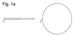
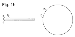
本発明の第1実施形態の場合、支持ウェハ1が最初に仮貼り合わせ層2によって被覆される。仮貼り合わせ層2は、有利にはSiO2である。この被覆は、どのような公知の被覆方法によって行ってもよいが、有利であるのはPVD,CVD或いは電気化学堆積法である。仮貼り合わせ層2の厚さは様々なパラメータに依存するが、1nm〜1mmの間にある。仮貼り合わせ層2の厚さは1nm〜1mmであり、有利には10nm〜100μm、いっそう有利には100nm〜10μm、最も有利には1μm〜5μmである。仮貼り合わせ層2には、この分野の当業者に知られた方法によって構造が形成される。
In the case of the first embodiment of the present invention, the
一例として図1cには、構造が形成された仮貼り合わせ層2がダクト3とともに描かれている。これらのダクト3は例えば公知のマスク技術即ちリソグラフィ及びマスキングを行い、その後、酸及び/又はアルカリによって、及び/又は相応に適切な化学物質によってエッチングすることにより、製造することができる。
As an example, in FIG. 1 c, a
本発明によれば、構造が形成された仮貼り合わせ層2を、シャドウマスクを用いることで堆積プロセス中にただちに製造することも考えられる。この場合、シャドウマスクによって、堆積プロセス中に材料を付着させるべきではない領域がマスキングされる。シャドウマスクを使用することにより、その後、仮貼り合わせ層2を面全体にわたりマスキングしてエッチングする必要がなくなる。
According to the invention, it is also conceivable to produce the
エッチングは特に、液体状態及び/又は蒸気状態のフッ化水素酸(フッ化水素、HF)によって行われる。特に蒸気相であると、ダクト3及び/又は設けられた孔を介して、フッ化水素酸が著しく速く進入するようになる。
Etching is performed in particular with hydrofluoric acid (hydrogen fluoride, HF) in the liquid state and / or vapor state. Particularly in the vapor phase, hydrofluoric acid enters significantly faster through the
本発明によって適用可能な酸をさらに挙げるとすれば、硫酸、塩酸、硝酸、燐酸、すべての有機酸である。 Further acids that can be applied according to the invention are sulfuric acid, hydrochloric acid, nitric acid, phosphoric acid, all organic acids.
別の選択肢として、複数の化学物質から成る公知の混合物も考えられ、例えば王水、ピラニア溶液(H2SO4+H2O2)、フッ化水素酸と硝酸の混合物も考えられる。 As another option, a known mixture of a plurality of chemical substances is also conceivable, such as aqua regia, piranha solution (H 2 SO 4 + H 2 O 2 ), a mixture of hydrofluoric acid and nitric acid.
エッチング媒体として、例えばKOH、TMAH(テトラメチルアンモニウムヒドロキシド)及び/又はEDP(エチレンジアミンピロカテコール)といった塩基性物質も用いられる。 As the etching medium, basic substances such as KOH, TMAH (tetramethylammonium hydroxide) and / or EDP (ethylenediamine pyrocatechol) are also used.
約85℃のとき、44%のKOH溶液によってSiO2に作用させたときのエッチングレートは、毎分約14オングストロームである。 At about 85 ° C., the etching rate when acting on SiO 2 with a 44% KOH solution is about 14 angstroms per minute.
約80℃のとき、25%のTMAH溶液によってSiO2に作用させたときのエッチングレートは、毎分約2オングストロームである。 At about 80 ° C., the etching rate when acting on SiO 2 with 25% TMAH solution is about 2 angstroms per minute.
約115℃のとき、EDP溶液によってSiO2に作用させたときのエッチングレートは、毎分約2オングストロームである。 At about 115 ° C., the etching rate when acting on SiO 2 with an EDP solution is about 2 angstroms per minute.
このようにエッチングレートが低いことから、本発明によればいっそう高い濃度及び/又はいっそう高い動作温度が要求される。ここで使用される溶液の濃度は20%よりも高く、有利には40%よりも高く、いっそう有利には60%よりも高く、著しく有利には80%よりも高く、最も有利には99%よりも高い。 Because of this low etching rate, the present invention requires higher concentrations and / or higher operating temperatures. The concentration of the solution used here is higher than 20%, preferably higher than 40%, more preferably higher than 60%, significantly higher than 80%, most preferably 99%. Higher than.
また、本発明によって適用されるエッチング温度は25℃よりも高く、有利には50℃よりも高く、いっそう有利には100℃よりも高く、著しく有利には200℃よりも高く、最も有利には400℃よりも高い。 Also, the etching temperature applied according to the invention is higher than 25 ° C., preferably higher than 50 ° C., more preferably higher than 100 ° C., significantly higher than 200 ° C., most preferably It is higher than 400 ° C.
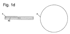
ついで製品ウェハ4の表面4oを、仮貼り合わせ層2の表面2oと接合することができる。一般的にはポリマーが使われる接着剤による接合とは異なり、ここでの接合は、有利にはSiO2である高温用に設計された仮貼り合わせ層2と、製品ウェハ4の表面4oとの間で行われる。融着接合技術及び陽極接合技術は当業者に知られている。融着接合或いは陽極接合は極めて強いので、背面4uを処理することができる。一例として、製品ウェハ4の背面薄化を挙げておく。融着接合は理想的には、力の作用を伴うことなく室温で実施され、つまり特にもっぱら仮貼り合わせ層2の表面と支持ウェハ1の表面との単純な接触によって実施される。陽極接合は大抵の場合、力を加えながらいっそう高い温度で実施される。
Subsequently, the surface 4o of the
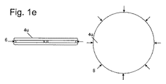
製品ウェハ4の処理後、製品ウェハ4を以下のようにして再び仮貼り合わせ層2から剥がすことができる。即ちこの場合、ダクト3を通して化学物質6を浸入させて、仮貼り合わせ層2を溶解させるか、或いは少なくとも、製品ウェハ4の表面4oと仮貼り合わせ層2の表面2oとの界面を弱めるようにする(図1d〜1f)。この場合、ダクト3の役割は主として、化学物質が仮貼り合わせ層2へいっそう入りやすくすることである。化学物質によって仮貼り合わせ層2が溶解され、それによって製品ウェハ4を支持ウェハ1から分離できるようになる。この支持ウェハ1は再利用可能である。仮貼り合わせ層2の残留物が支持ウェハ1に存在している場合、本発明によれば支持ウェハ1を洗浄することができる。
After the
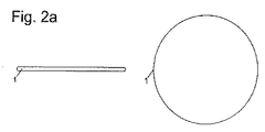
別の実施形態(図2a〜c)によれば、被覆プロセス有利にはCVD被覆プロセスによって、仮貼り合わせ層2′が支持ウェハ1に被着される。CVD被覆プロセスが適用されるならば、堆積した層はすでにそれ相応に高い多孔性を有している。他の被覆プロセスを適用した場合、本発明によれば周知のプロセスによってそれ相応の多孔性を生じさせる必要がある。これら多数の孔に、種々の気体を取り込むことができ、或いはすでに被覆プロセス中に封入することができる。融着プロセスによって、製品ウェハ4が仮貼り合わせ層2′と溶接される。したがって、製品ウェハ4の裏面を処理することができる。クリティカルな温度Tkを超えて加熱することにより、仮貼り合わせ層2′中の気体が伸長する。このようにして体積が伸長することによって、仮貼り合わせ層2′の少なくとも大部分が割れることになり、及び/又は仮貼り合わせ層2′の表面2o′と製品ウェハ4の表面4oとの界面が弱くなり、製品ウェハ4を支持ウェハ1から、いっそう正確には仮貼り合わせ層2′から、分離できるようになる。発生したガスによって、必ずしも界面全体の剥離が引き起こされるようにしなくてもよい。本発明によれば、ガス発生プロセスによって界面(仮貼り合わせ層2′)が弱まり、その後で例えば機械的な分離プロセスを行うことによって、両方のウェハ1,4が互いに分離されれば、十分である(図2d〜図2f参照)。したがってクリティカルな温度Tkを、おおよそ製品ウェハ4が処理される温度範囲にすることもでき、そのようにした場合、例えば製品ウェハ4の処理中にガスが発生するようになる。
According to another embodiment (FIGS. 2 a-c), a
さらに別の実施形態によれば(図3)、仮貼り合わせ層2″有利にはSiO2層の面全体にわたりそれぞれ異なる領域Rx(ここでxは1,2,3)の表面Rox(ここでxは1,2,3)を設け、それらの表面Roxに、それぞれ異なる物理的及び/又は化学的な処理を施すことで、それに続く接合プロセスにより、個々の領域Rxにそれぞれ異なる強さの接合力を生じさせる。ここでは一例として、ただし他を排除するものではないが、以下の表面処理を挙げておく:プラズマプロセス、コーティングプロセス、表面粗面度を変化させるプロセス。
According to a further embodiment (FIG. 3), the surface Ro x (wherein x is 1, 2, 3) in different regions R x (where x is 1, 2, 3) over the entire surface of the
さらに別の実施形態によれば、製品基板4と支持基板1との接合が陽極接合法によって行われる。これによれば、陽イオンと陰イオンの移動によってシロキサン結合Si−O−Siの形成が引き起こされ、これによって仮貼り合わせ層2を介して、製品基板4が支持基板1と溶接される。第1の実施形態によれば、支持基板1はガラス基板1であり、仮貼り合わせ層2,2′,2″は少なくとも大部分が、有利には全体が、ケイ素から成る。第2の実施形態によれば、支持基板1はケイ素基板1であり、仮貼り合わせ層2,2′,2″は少なくとも大部分が、有利には全体が、ガラスから成る。仮貼り合わせ層2,2′,2″を、本発明による他の実施形態によるSiO2層と同様に事前に処理することができる。
According to yet another embodiment, the
1 支持ウェハ
2,2′,2″ 仮貼り合わせ層
2o,2o′,2o″ 表面
3 ダクト
4 製品ウェハ
4o 表面
4u 裏面
6 溶剤
Rx 領域
Rox 表面
1
Claims (8)
以下のステップ特に以下のフローを含み、即ち
融着接合又は陽極接合に適した仮貼り合わせ層(2,2′,2″)を支持ウェハ(1)に被着する被着ステップと、
前記被着ステップ中及び/又は前記被着ステップ後、前記仮貼り合わせ層(2,2′,2″)の一時的な接合を解除できるように、該仮貼り合わせ層(2,2′,2″)を変形させる変形ステップと
を含むことを特徴とする、
仮貼り合わせ層(2,2′,2″)を支持ウェハ(1)に被着する方法。 In a method of depositing a temporary bonding layer (2, 2 ′, 2 ″) on a support wafer (1) for temporary bonding to a product wafer (4) by fusion bonding or anodic bonding,
The following steps, in particular including the following flow: a deposition step for depositing a temporary bonding layer (2, 2 ′, 2 ″) suitable for fusion bonding or anodic bonding on the support wafer (1);
During the deposition step and / or after the deposition step, the temporary bonding layer (2, 2 ′, 2 ″, so that the temporary bonding of the temporary bonding layer (2, 2 ′, 2 ″) can be released. 2 ″), and a deformation step for deforming.
A method of depositing the temporary bonding layer (2, 2 ′, 2 ″) on the support wafer (1).
Applications Claiming Priority (3)
| Application Number | Priority Date | Filing Date | Title |
|---|---|---|---|
| DE102012112989.4A DE102012112989A1 (en) | 2012-12-21 | 2012-12-21 | Method for applying a temporary boundary layer |
| DE102012112989.4 | 2012-12-21 | ||
| PCT/EP2013/076629 WO2014095668A1 (en) | 2012-12-21 | 2013-12-16 | Method for applying a temporary bonding layer |
Publications (2)
| Publication Number | Publication Date |
|---|---|
| JP2016503961A true JP2016503961A (en) | 2016-02-08 |
| JP2016503961A5 JP2016503961A5 (en) | 2017-01-19 |
Family
ID=49883069
Family Applications (1)
| Application Number | Title | Priority Date | Filing Date |
|---|---|---|---|
| JP2015548392A Pending JP2016503961A (en) | 2012-12-21 | 2013-12-16 | Method for applying temporary bonding layer |
Country Status (8)
| Country | Link |
|---|---|
| US (1) | US20150047784A1 (en) |
| JP (1) | JP2016503961A (en) |
| KR (1) | KR20150097381A (en) |
| CN (1) | CN104380457A (en) |
| AT (1) | AT516064B1 (en) |
| DE (1) | DE102012112989A1 (en) |
| SG (1) | SG2014013056A (en) |
| WO (1) | WO2014095668A1 (en) |
Families Citing this family (4)
| Publication number | Priority date | Publication date | Assignee | Title |
|---|---|---|---|---|
| KR102507283B1 (en) | 2015-12-22 | 2023-03-07 | 삼성전자주식회사 | A substrate chuck and a substrate bonding system including the same |
| JP2017163009A (en) * | 2016-03-10 | 2017-09-14 | 東芝メモリ株式会社 | Method of manufacturing semiconductor device |
| US10676350B2 (en) | 2018-09-21 | 2020-06-09 | ColdQuanta, Inc. | Reversible anodic bonding |
| DE102023000322A1 (en) | 2022-10-05 | 2024-04-11 | Luce Patent Gmbh | Process for the material and energetic utilization of solid residues from the methane fermentation of plant parts |
Citations (4)
| Publication number | Priority date | Publication date | Assignee | Title |
|---|---|---|---|---|
| JPH07263291A (en) * | 1994-01-26 | 1995-10-13 | Commiss Energ Atom | Substrate for integrated parts constituted of thin film and its manufacture |
| JP2005142504A (en) * | 2003-11-10 | 2005-06-02 | Sony Corp | Semiconductor device, semiconductor substrate, and their manufacturing method |
| JP2007322575A (en) * | 2006-05-31 | 2007-12-13 | Hitachi Displays Ltd | Display device |
| JP2009516863A (en) * | 2005-11-22 | 2009-04-23 | コミサリヤ・ア・レネルジ・アトミク | Method for manufacturing a screen-type flexible electronic device comprising a plurality of thin film components |
Family Cites Families (10)
| Publication number | Priority date | Publication date | Assignee | Title |
|---|---|---|---|---|
| JP3257580B2 (en) * | 1994-03-10 | 2002-02-18 | キヤノン株式会社 | Manufacturing method of semiconductor substrate |
| JPH09260342A (en) * | 1996-03-18 | 1997-10-03 | Mitsubishi Electric Corp | Method and apparatus for manufacturing semiconductor device |
| JP4439602B2 (en) * | 1997-09-29 | 2010-03-24 | 株式会社東芝 | Manufacturing method of semiconductor device |
| DE19958803C1 (en) * | 1999-12-07 | 2001-08-30 | Fraunhofer Ges Forschung | Method and device for handling semiconductor substrates during processing and / or processing |
| US6853129B1 (en) * | 2000-07-28 | 2005-02-08 | Candescent Technologies Corporation | Protected substrate structure for a field emission display device |
| DE10060433B4 (en) * | 2000-12-05 | 2006-05-11 | Hahn-Schickard-Gesellschaft für angewandte Forschung e.V. | Method for producing a fluid component, fluid component and analysis device |
| FR2823596B1 (en) * | 2001-04-13 | 2004-08-20 | Commissariat Energie Atomique | SUBSTRATE OR DISMOUNTABLE STRUCTURE AND METHOD OF MAKING SAME |
| US7087134B2 (en) * | 2004-03-31 | 2006-08-08 | Hewlett-Packard Development Company, L.P. | System and method for direct-bonding of substrates |
| EP1605502A1 (en) * | 2004-06-08 | 2005-12-14 | Interuniversitair Microelektronica Centrum Vzw | Transfer method for the manufacturing of electronic devices |
| US9299594B2 (en) * | 2010-07-27 | 2016-03-29 | Taiwan Semiconductor Manufacturing Company, Ltd. | Substrate bonding system and method of modifying the same |
-
2012
- 2012-12-21 DE DE102012112989.4A patent/DE102012112989A1/en not_active Ceased
-
2013
- 2013-12-16 AT ATA9019/2013A patent/AT516064B1/en active
- 2013-12-16 US US14/388,107 patent/US20150047784A1/en not_active Abandoned
- 2013-12-16 CN CN201380018729.5A patent/CN104380457A/en active Pending
- 2013-12-16 WO PCT/EP2013/076629 patent/WO2014095668A1/en active Application Filing
- 2013-12-16 JP JP2015548392A patent/JP2016503961A/en active Pending
- 2013-12-16 KR KR1020147027831A patent/KR20150097381A/en not_active Application Discontinuation
- 2013-12-16 SG SG2014013056A patent/SG2014013056A/en unknown
Patent Citations (4)
| Publication number | Priority date | Publication date | Assignee | Title |
|---|---|---|---|---|
| JPH07263291A (en) * | 1994-01-26 | 1995-10-13 | Commiss Energ Atom | Substrate for integrated parts constituted of thin film and its manufacture |
| JP2005142504A (en) * | 2003-11-10 | 2005-06-02 | Sony Corp | Semiconductor device, semiconductor substrate, and their manufacturing method |
| JP2009516863A (en) * | 2005-11-22 | 2009-04-23 | コミサリヤ・ア・レネルジ・アトミク | Method for manufacturing a screen-type flexible electronic device comprising a plurality of thin film components |
| JP2007322575A (en) * | 2006-05-31 | 2007-12-13 | Hitachi Displays Ltd | Display device |
Also Published As
| Publication number | Publication date |
|---|---|
| CN104380457A (en) | 2015-02-25 |
| AT516064B1 (en) | 2016-02-15 |
| SG2014013056A (en) | 2014-10-30 |
| WO2014095668A1 (en) | 2014-06-26 |
| KR20150097381A (en) | 2015-08-26 |
| DE102012112989A1 (en) | 2014-06-26 |
| AT516064A5 (en) | 2016-02-15 |
| US20150047784A1 (en) | 2015-02-19 |
Similar Documents
| Publication | Publication Date | Title |
|---|---|---|
| JP5274859B2 (en) | Manufacturing method of bonded substrate | |
| Zahedinejad et al. | Deep and vertical silicon bulk micromachining using metal assisted chemical etching | |
| JPH11195773A (en) | Substrate processing method and apparatus thereof, and soi substrate | |
| JP2016503961A (en) | Method for applying temporary bonding layer | |
| TW201806082A (en) | Articles and methods of forming vias in substrates | |
| Guan et al. | Stress control of plasma enhanced chemical vapor deposited silicon oxide film from tetraethoxysilane | |
| TW201201248A (en) | Process and structure for high temperature selective fusion bonding | |
| Sammak et al. | Deep vertical etching of silicon wafers using a hydrogenation-assisted reactive ion etching | |
| JP2012040684A (en) | Micromechanical device and its manufacturing method | |
| US10854494B2 (en) | Method for producing an interface intended to assemble temporarily a microelectronic support and a manipulation handle, and temporary assembly interface | |
| JP6281883B2 (en) | Package formation method | |
| US20080176382A1 (en) | Process of forming and controlling rough interfaces | |
| Christophersen et al. | Deep electrochemical trench etching with organic hydrofluoric electrolytes | |
| RU2285748C2 (en) | Method of manufacture of composite membranes on base of thin films of metals | |
| TW201005883A (en) | Method for manufacturing soi wafer | |
| US7087456B2 (en) | Stiction resistant release process | |
| CN104934293B (en) | A kind of metallic layer graphic method | |
| JP4598413B2 (en) | Method for manufacturing bonded wafer and jig for removing oxide film from bonded wafer | |
| RU2804791C1 (en) | Method for manufacturing deep-profile multilevel microstructures in quartz glass | |
| Burham et al. | Effect of temperature on the etching rate of nitride and oxide layer using Buffered Oxide Etch | |
| WO2014161462A1 (en) | Method for reinforcing micro-electro-mechanical systems device in manufacturing process | |
| CN104627949A (en) | Microelectronic mechanical system structure forming method | |
| JP2008244323A (en) | Stencil mask | |
| JP3320379B2 (en) | Manufacturing method of bonded substrate | |
| JP5531973B2 (en) | Bonded substrate and manufacturing method thereof |
Legal Events
| Date | Code | Title | Description |
|---|---|---|---|
| A521 | Request for written amendment filed |
Free format text: JAPANESE INTERMEDIATE CODE: A523 Effective date: 20161128 |
|
| A621 | Written request for application examination |
Free format text: JAPANESE INTERMEDIATE CODE: A621 Effective date: 20161128 |
|
| A977 | Report on retrieval |
Free format text: JAPANESE INTERMEDIATE CODE: A971007 Effective date: 20171020 |
|
| A131 | Notification of reasons for refusal |
Free format text: JAPANESE INTERMEDIATE CODE: A131 Effective date: 20171030 |
|
| A02 | Decision of refusal |
Free format text: JAPANESE INTERMEDIATE CODE: A02 Effective date: 20180528 |