JP2016201835A - Surface scattering antenna - Google Patents
Surface scattering antenna Download PDFInfo
- Publication number
- JP2016201835A JP2016201835A JP2016144675A JP2016144675A JP2016201835A JP 2016201835 A JP2016201835 A JP 2016201835A JP 2016144675 A JP2016144675 A JP 2016144675A JP 2016144675 A JP2016144675 A JP 2016144675A JP 2016201835 A JP2016201835 A JP 2016201835A
- Authority
- JP
- Japan
- Prior art keywords
- antenna
- scattering
- wave
- positions
- control inputs
- Prior art date
- Legal status (The legal status is an assumption and is not a legal conclusion. Google has not performed a legal analysis and makes no representation as to the accuracy of the status listed.)
- Granted
Links
- 238000000034 method Methods 0.000 claims abstract description 151
- 230000008878 coupling Effects 0.000 claims abstract description 14
- 238000010168 coupling process Methods 0.000 claims abstract description 14
- 238000005859 coupling reaction Methods 0.000 claims abstract description 14
- 238000005286 illumination Methods 0.000 claims description 58
- 238000004891 communication Methods 0.000 claims description 49
- 230000033001 locomotion Effects 0.000 claims description 21
- 230000007613 environmental effect Effects 0.000 claims description 10
- 238000012545 processing Methods 0.000 claims description 6
- 230000001902 propagating effect Effects 0.000 claims description 6
- 238000003860 storage Methods 0.000 claims description 6
- 239000004973 liquid crystal related substance Substances 0.000 abstract description 44
- 239000000463 material Substances 0.000 abstract description 19
- 230000000295 complement effect Effects 0.000 abstract description 15
- 239000004020 conductor Substances 0.000 description 28
- 238000010586 diagram Methods 0.000 description 24
- 230000005684 electric field Effects 0.000 description 16
- 230000008569 process Effects 0.000 description 16
- 230000006870 function Effects 0.000 description 13
- 230000004044 response Effects 0.000 description 12
- 230000005284 excitation Effects 0.000 description 10
- 239000011159 matrix material Substances 0.000 description 7
- 239000013598 vector Substances 0.000 description 7
- 238000004590 computer program Methods 0.000 description 6
- 230000000670 limiting effect Effects 0.000 description 6
- 230000005855 radiation Effects 0.000 description 6
- 238000009826 distribution Methods 0.000 description 5
- 210000000554 iris Anatomy 0.000 description 5
- 229920000642 polymer Polymers 0.000 description 5
- 239000004642 Polyimide Substances 0.000 description 4
- 238000005530 etching Methods 0.000 description 4
- 238000002347 injection Methods 0.000 description 4
- 239000007924 injection Substances 0.000 description 4
- 238000012986 modification Methods 0.000 description 4
- 230000004048 modification Effects 0.000 description 4
- 229920001721 polyimide Polymers 0.000 description 4
- 239000004983 Polymer Dispersed Liquid Crystal Substances 0.000 description 3
- 230000008901 benefit Effects 0.000 description 3
- 230000005540 biological transmission Effects 0.000 description 3
- 230000009977 dual effect Effects 0.000 description 3
- 230000000694 effects Effects 0.000 description 3
- 238000005516 engineering process Methods 0.000 description 3
- 229910052751 metal Inorganic materials 0.000 description 3
- 239000002184 metal Substances 0.000 description 3
- 230000001681 protective effect Effects 0.000 description 3
- 238000007493 shaping process Methods 0.000 description 3
- 125000006850 spacer group Chemical group 0.000 description 3
- 239000000758 substrate Substances 0.000 description 3
- 239000010409 thin film Substances 0.000 description 3
- RYGMFSIKBFXOCR-UHFFFAOYSA-N Copper Chemical compound [Cu] RYGMFSIKBFXOCR-UHFFFAOYSA-N 0.000 description 2
- 150000001875 compounds Chemical class 0.000 description 2
- 238000007796 conventional method Methods 0.000 description 2
- 229910052802 copper Inorganic materials 0.000 description 2
- 239000010949 copper Substances 0.000 description 2
- 239000003989 dielectric material Substances 0.000 description 2
- 238000007373 indentation Methods 0.000 description 2
- 230000006698 induction Effects 0.000 description 2
- 238000004519 manufacturing process Methods 0.000 description 2
- 239000000203 mixture Substances 0.000 description 2
- 239000002245 particle Substances 0.000 description 2
- 230000002093 peripheral effect Effects 0.000 description 2
- 238000000206 photolithography Methods 0.000 description 2
- 239000005212 4-Cyano-4'-pentylbiphenyl Substances 0.000 description 1
- HHPCNRKYVYWYAU-UHFFFAOYSA-N 4-cyano-4'-pentylbiphenyl Chemical group C1=CC(CCCCC)=CC=C1C1=CC=C(C#N)C=C1 HHPCNRKYVYWYAU-UHFFFAOYSA-N 0.000 description 1
- VYZAMTAEIAYCRO-UHFFFAOYSA-N Chromium Chemical compound [Cr] VYZAMTAEIAYCRO-UHFFFAOYSA-N 0.000 description 1
- 239000004988 Nematic liquid crystal Substances 0.000 description 1
- 238000013459 approach Methods 0.000 description 1
- 238000000429 assembly Methods 0.000 description 1
- 230000000712 assembly Effects 0.000 description 1
- 239000003990 capacitor Substances 0.000 description 1
- 230000008859 change Effects 0.000 description 1
- 238000006243 chemical reaction Methods 0.000 description 1
- 229910052804 chromium Inorganic materials 0.000 description 1
- 239000011651 chromium Substances 0.000 description 1
- 238000005352 clarification Methods 0.000 description 1
- 230000001419 dependent effect Effects 0.000 description 1
- 238000000151 deposition Methods 0.000 description 1
- 238000013461 design Methods 0.000 description 1
- 238000007772 electroless plating Methods 0.000 description 1
- 230000005672 electromagnetic field Effects 0.000 description 1
- 238000009713 electroplating Methods 0.000 description 1
- 230000005496 eutectics Effects 0.000 description 1
- 239000000835 fiber Substances 0.000 description 1
- 239000010408 film Substances 0.000 description 1
- PCHJSUWPFVWCPO-UHFFFAOYSA-N gold Chemical compound [Au] PCHJSUWPFVWCPO-UHFFFAOYSA-N 0.000 description 1
- 239000010931 gold Substances 0.000 description 1
- 229910052737 gold Inorganic materials 0.000 description 1
- 238000001093 holography Methods 0.000 description 1
- 238000002955 isolation Methods 0.000 description 1
- 238000003754 machining Methods 0.000 description 1
- 239000000696 magnetic material Substances 0.000 description 1
- 230000007246 mechanism Effects 0.000 description 1
- 230000028161 membrane depolarization Effects 0.000 description 1
- 239000003607 modifier Substances 0.000 description 1
- 239000002991 molded plastic Substances 0.000 description 1
- 230000005404 monopole Effects 0.000 description 1
- 238000000465 moulding Methods 0.000 description 1
- 230000003287 optical effect Effects 0.000 description 1
- 230000008520 organization Effects 0.000 description 1
- 230000036961 partial effect Effects 0.000 description 1
- 238000000059 patterning Methods 0.000 description 1
- 150000003071 polychlorinated biphenyls Chemical class 0.000 description 1
- 239000004810 polytetrafluoroethylene Substances 0.000 description 1
- 229920001343 polytetrafluoroethylene Polymers 0.000 description 1
- 230000002829 reductive effect Effects 0.000 description 1
- 238000000611 regression analysis Methods 0.000 description 1
- 239000011347 resin Substances 0.000 description 1
- 229920005989 resin Polymers 0.000 description 1
- 230000002441 reversible effect Effects 0.000 description 1
- 238000004088 simulation Methods 0.000 description 1
- 230000003068 static effect Effects 0.000 description 1
- 238000012360 testing method Methods 0.000 description 1
- 229920001187 thermosetting polymer Polymers 0.000 description 1
- 230000007704 transition Effects 0.000 description 1
Images


Classifications
-
- H—ELECTRICITY
- H01—ELECTRIC ELEMENTS
- H01Q—ANTENNAS, i.e. RADIO AERIALS
- H01Q13/00—Waveguide horns or mouths; Slot antennas; Leaky-waveguide antennas; Equivalent structures causing radiation along the transmission path of a guided wave
- H01Q13/20—Non-resonant leaky-waveguide or transmission-line antennas; Equivalent structures causing radiation along the transmission path of a guided wave
- H01Q13/28—Non-resonant leaky-waveguide or transmission-line antennas; Equivalent structures causing radiation along the transmission path of a guided wave comprising elements constituting electric discontinuities and spaced in direction of wave propagation, e.g. dielectric elements or conductive elements forming artificial dielectric
-
- H—ELECTRICITY
- H01—ELECTRIC ELEMENTS
- H01Q—ANTENNAS, i.e. RADIO AERIALS
- H01Q15/00—Devices for reflection, refraction, diffraction or polarisation of waves radiated from an antenna, e.g. quasi-optical devices
- H01Q15/0006—Devices acting selectively as reflecting surface, as diffracting or as refracting device, e.g. frequency filtering or angular spatial filtering devices
- H01Q15/006—Selective devices having photonic band gap materials or materials of which the material properties are frequency dependent, e.g. perforated substrates, high-impedance surfaces
- H01Q15/0066—Selective devices having photonic band gap materials or materials of which the material properties are frequency dependent, e.g. perforated substrates, high-impedance surfaces said selective devices being reconfigurable, tunable or controllable, e.g. using switches
-
- H—ELECTRICITY
- H01—ELECTRIC ELEMENTS
- H01Q—ANTENNAS, i.e. RADIO AERIALS
- H01Q15/00—Devices for reflection, refraction, diffraction or polarisation of waves radiated from an antenna, e.g. quasi-optical devices
- H01Q15/0006—Devices acting selectively as reflecting surface, as diffracting or as refracting device, e.g. frequency filtering or angular spatial filtering devices
- H01Q15/0086—Devices acting selectively as reflecting surface, as diffracting or as refracting device, e.g. frequency filtering or angular spatial filtering devices said selective devices having materials with a synthesized negative refractive index, e.g. metamaterials or left-handed materials
-
- H—ELECTRICITY
- H01—ELECTRIC ELEMENTS
- H01Q—ANTENNAS, i.e. RADIO AERIALS
- H01Q15/00—Devices for reflection, refraction, diffraction or polarisation of waves radiated from an antenna, e.g. quasi-optical devices
- H01Q15/02—Refracting or diffracting devices, e.g. lens, prism
-
- H—ELECTRICITY
- H01—ELECTRIC ELEMENTS
- H01Q—ANTENNAS, i.e. RADIO AERIALS
- H01Q15/00—Devices for reflection, refraction, diffraction or polarisation of waves radiated from an antenna, e.g. quasi-optical devices
- H01Q15/02—Refracting or diffracting devices, e.g. lens, prism
- H01Q15/10—Refracting or diffracting devices, e.g. lens, prism comprising three-dimensional array of impedance discontinuities, e.g. holes in conductive surfaces or conductive discs forming artificial dielectric
-
- H—ELECTRICITY
- H01—ELECTRIC ELEMENTS
- H01Q—ANTENNAS, i.e. RADIO AERIALS
- H01Q3/00—Arrangements for changing or varying the orientation or the shape of the directional pattern of the waves radiated from an antenna or antenna system
Abstract
Description
〔関連する出願についての相互参照〕
本願は、以下に記載した出願(“関連出願”)に基づく最先の有効出願日の利益に関連し、その利益を主張する(例えば、本願は、仮特許出願以外の最先の有効な優先日を主張するか、仮特許出願、関連出願の任意のすべての親出願、その親出願、さらにその親出願等に対して、合衆国法典35巻第119条(e)に基づく利益を主張する)。関連出願、および関連出願の任意のすべての親出願、その親出願、さらにその親出願等のうち、いかなる優先権の主張をするものであっても、すべての内容は本明細書と矛盾しないような内容の範囲内で参照によって本明細書に含まれる。
[Cross-reference for related applications]
This application relates to and claims the benefit of the earliest effective filing date based on the application described below (“Related Application”) (eg, this application is the earliest valid priority other than the provisional patent application). Or claim the benefit of the provisional patent application, any parent application of the related application, its parent application, and its parent application, etc. under 35 USC 35, 119 (e)) . The related application and any parent application of the related application, the parent application, and the parent application, etc., any claim of priority shall not be inconsistent with this specification. Are included herein by reference within the scope of such content.
〔関連出願〕
USPTOの特別な法的要件のために、本願は、米国特許出願第61/455,171号(発明の名称:「表面散乱アンテナ」、発明者:NATHAN KUNDTZら、出願日:2010年10月15日、現在同時係属)の一部継続出願を構成しているか、または現在同時係属している出願に出願日の利益を得る権利が付与される出願である。
[Related applications]
Due to the special legal requirements of the USPTO, this application is based on US patent application 61 / 455,171 (Title: “Surface Scattering Antenna”, Inventor: NATHAN KUNDTZ et al., Filing date: October 15, 2010). Application that is part of a continuation-in-part application, or that is currently co-pending, and is entitled to the benefit of filing date.
米国特許商標庁(USPTO)は、USPTOのコンピュータプログラムにおいて、特許出願人が整理番号と、出願が継続出願であるか、一部継続出願であるか、または親出願の分割出願であるかということとの双方を示すことが必要となることに関する通知を発表した。これはStephen G. Kuninによる「先願の利益」と題された通知(2003年3月18日付のUSPTO官報)である。本願の出願団体(以下、「出願人」)は、法令に則って優先権が主張されている出願に対する特定の参照を以上で示している。出願人は、法令の示す具体的な参照の文言は一義的であり、米国特許出願の優先権を主張するために整理番号または「継続中」あるいは「一部継続中」等のいかなる説明も必要しないと理解している。しかしながら、出願人は、USPTOのコンピュータプログラムが一定のデータ入力要求を有すると理解しているので、上記のように本願とその親出願との関係を表示するが、このような表示は、本願がその親出願の事項に加えて何らかの新規事項を含んでいるかどうかに関して、何らかの注釈および/または自認をするものというように解釈されるべきではない。 The US Patent and Trademark Office (USPTO) states that in the USPTO computer program, the patent applicant is assigned a serial number and whether the application is a continuation application, a partial continuation application, or a divisional application of a parent application. Announced a notice regarding the need to show both. This is because Stephen G. This is a notice (USPTO official gazette dated 18 March 2003) entitled “Profit of Prior Application” by Kunin. The application organization of the present application (hereinafter “applicant”) has given above specific references to applications for which priority is claimed in accordance with the law. Applicants are unambiguous in the language of the specific references indicated by the statute and need any reference number or any explanation such as “ongoing” or “partially ongoing” to claim priority of a US patent application I understand not to. However, since the applicant understands that the USPTO computer program has a certain data input request, the relationship between the present application and its parent application is displayed as described above. It should not be construed as any note and / or self-approval regarding whether it contains any new matter in addition to the matter of its parent application.
〔図面の簡単な説明〕
図1は、表面散乱アンテナを示す概略図である。
[Brief description of the drawings]
FIG. 1 is a schematic diagram showing a surface scattering antenna.
図2Aおよび2Bは、それぞれ表面散乱アンテナの模範的な調整パターンと、対応するビームパターンとを示す図である。 2A and 2B are diagrams showing an exemplary adjustment pattern of a surface scattering antenna and a corresponding beam pattern, respectively.
図3Aおよび3Bは、それぞれ表面散乱アンテナの他の模範的な調整パターンと、対応するビームパターンとを示す図である。 3A and 3B are diagrams showing another exemplary adjustment pattern of a surface scattering antenna and a corresponding beam pattern, respectively.
図4Aおよび4Bはそれぞれ、表面散乱アンテナの他の模範的な調整パターンと、対応するフィールドパターンとを示す図である。 4A and 4B are diagrams showing another exemplary adjustment pattern of a surface scattering antenna and a corresponding field pattern, respectively.
図5および図6は、表面散乱アンテナのユニットセルを示す図である。 5 and 6 are diagrams showing a unit cell of the surface scattering antenna.
図7は、メタマテリアル要素の例を示す図である。 FIG. 7 is a diagram illustrating an example of a metamaterial element.
図8は、表面散乱アンテナのマイクロストリップの実施形態を示す図である。 FIG. 8 is a diagram showing a microstrip embodiment of a surface scattering antenna.
図9は、表面散乱アンテナの共面導波管の実施形態を示す図である。 FIG. 9 is a diagram showing an embodiment of a coplanar waveguide of a surface scattering antenna.
図10および図11は、表面散乱アンテナの閉塞導波管の実施形態を示す図である。 10 and 11 are diagrams showing an embodiment of a closed waveguide of a surface scattering antenna.
図12は、散乱素子の直接アドレス指定を用いた表面散乱アンテナを示す図である。 FIG. 12 shows a surface scattering antenna using direct addressing of scattering elements.
図13は、散乱素子の行列アドレス指定を用いた表面散乱アンテナを示す図である。 FIG. 13 is a diagram illustrating a surface scattering antenna using matrix addressing of scattering elements.
図14は、システムブロック図を示す図である。 FIG. 14 is a diagram showing a system block diagram.
図15および図16は、フロー図を示す図である。 15 and 16 are flowcharts.
〔詳細な説明〕
以下の詳細な説明では、本明細書の一部を構成する添付図面を参照している。図面において、類似の記号は、特に断りがない限り、類似の構成要素を通常は特定している。詳細な説明、図面、および特許請求の範囲に記載されている例示的な実施形態は、限定することを意図していない。本明細書に示されている事項の精神または範囲から逸脱することなく、他の実施形態が利用されてもよいし、また他の変更がなされてもよい。
[Detailed explanation]
In the following detailed description, references are made to the accompanying drawings that form a part hereof. In the drawings, similar symbols typically identify similar components, unless context dictates otherwise. The illustrative embodiments described in the detailed description, drawings, and claims are not meant to be limiting. Other embodiments may be utilized and other changes may be made without departing from the spirit or scope of the matters presented herein.
表面散乱アンテナの概略図が、図1に示されている。表面散乱アンテナ100は、波伝搬構造104に沿って配置された複数の散乱素子102a,102bを含んでいる。波伝搬構造104は、マイクロストリップ、共面導波管、平行板導波管、誘電体板、閉塞したまたは管状の導波管、もしくは構造に沿ってまたは構造内に誘導波または表面波105が伝搬するのを支持し得る構造であればいかなる構造であってもよい。状線105は、誘導波または表面波を象徴化して示したものであり、誘導波または表面波の実際の波長または振幅を示すことを意図していない。加えて、波状線105が波伝搬構造104内(例えば、誘導波について言えば金属製導波管内)に示されているが、表面波に関しては波伝搬構造の外側に実質的に局在し得る(例えば、TMモードでは1本のワイヤー伝送線上にあり、「疑似プラズモン」では人工的なインピーダンス表面上にあり得る)。散乱素子102a,102bは、波伝搬構造104内に組み込まれているか、波伝搬構造104の表面上に配置されているか、または波伝搬構造104のエバネッセント近傍に配置されたメタマテリアル要素を含んでいてもよい。例えば、散乱素子は、米国特許出願公開第2010/0156573号(D.R.Smithら「表面および導波管のためのメタマテリアル」)に開示されているような、相補的メタマテリアル要素を含むことができる。この文献は参照により本願に含まれる。
A schematic diagram of a surface scattering antenna is shown in FIG. The
表面散乱アンテナは、波伝搬構造104を給電構造108に連結するために構成された少なくとも1つの給電コネクタ106も含む。給電構造108(同軸ケーブルとして概略的に示されている)は、伝送線、導波管、または給電コネクタ106を経由して、波伝搬構造104の誘導波または表面波105に送り出され得る電磁信号を供給可能な構造であればいかなる構造であってもよい。給電コネクタ106は、例えば同軸マイクロストリップコネクタ(例えば、SMA−to−PCBアダプタ)、同軸導波管コネクタ、モード適合移行部等であってもよい。図1に「エンドランチ」構造の給電コネクタを示しており、当該構造により誘導波または表面波105が波伝搬構造の周辺領域(例えば、マイクロストリップの先端または平行板導波管の端部)から送り出され得る。しかし、別の実施形態においては、給電構造は、波伝搬構造の非周辺部に取り付けられていてもよく、それにより誘導波または表面波105は、波伝搬構造の非周辺部(例えば、マイクロストリップの中間点、または平行板導波管の上端または下端に空けられた穴)から送り出され得る。また、さらに別の実施形態では、複数の位置(波伝搬構造の周辺の位置および/または非周辺の位置)において波伝搬構造に取り付けられた複数の給電コネクタを提供してもよい。
The surface scattering antenna also includes at least one
散乱素子102a,102bは、1つ以上の外部入力に応じて調整可能な電磁特性を有する調整可能な散乱素子である。調整可能な散乱素子の様々な実施形態は、例えば既に参照したD.R.Smithらの文献に開示されており、本明細書にさらに開示されている。調整可能な散乱素子は、電圧入力(例えば、能動素子(例えば、バラクタ、トランジスタ、またはダイオード等)または管状誘電性物質を組み込む素子(例えば、強誘電体等)へのバイアス電圧)、電流入力(例えば、能動素子への荷電粒子の直接注入)、光入力(例えば、光活性物質の照明)、フィールド入力(例えば、非線形磁性体を含む素子への磁場)、機械的入力(例えば、MEMS、作動装置、または油圧技術)等に応じて調整可能な素子を含むことができる。図1の概略例では、第1電磁特性を有する第1状態に調整された散乱素子は、第1素子102aとして示されており、第2電磁特性を有する第2状態に調整された散乱素子は、第2素子102bとして示されている。第1および第2電磁特性に対応する第1および第2状態を有している散乱素子の図示は、制限することを意図していない。実施形態は、互いに異なる非連続の複数の電磁特性に対応した非連続の複数の状態の中から選択するために非連続的に調整可能である散乱素子、または互いに異なる連続の電磁特性に対応した連続の状態の中から選択するために連続的に調整可能な散乱素子を提供してもよい。さらに、図1に示されている調整の具体的形態(すなわち、素子102a,102bの交互配列)は、単に模範的な構成であり、制限することを意図していない。
The
図1の例において、散乱素子102a,102bは、それぞれ第1および第2電磁特性の関数である誘導波または表面波105への第1および第2結合を有している。例えば、第1および第2結合は、誘導波または表面波の周波数または周波数帯における散乱素子の第1および第2分極率であってもよい。1つの方法では、第1結合が実質的な非ゼロ結合であるのに対して、第2結合は実質的なゼロ結合である。別の方法では、両方の結合が実質的な非ゼロ結合であるが、第1結合が第2結合よりも実質的に大きい(または小さい)。第1および第2結合に起因して、第1および第2散乱素子102aおよび102bは、それぞれ第1および第2結合の関数(例えば、比例)である振幅を有する複数の散乱電磁波を形成するために誘導波または表面波105に対応する。散乱電磁波の重ね合わせは、本実施例において、表面散乱アンテナ100から放射する平面波110として示されている電磁波を備える。
In the example of FIG. 1, the
平面波の発生は、散乱素子の調整の具体的なパターン(例えば、図1における第1および第2散乱素子の交互の配置)を、平面波110を形成するために誘導波または表面波105を散乱させる格子を規定するパターンとして見なすことによって理解され得る。このパターンは調整可能なので、表面散乱アンテナのいくつかの実施形態は、調整可能な格子、またはより一般的にホログラムを提供してもよい。この場合、散乱素子の調整パターンは、ホログラフィの原則に従って選択され得る。例えば、誘導波または表面波が波伝搬構造104に沿った位置の関数である複素スカラ入力波Ψinによって表され、表面散乱アンテナが別の複素スカラ波Ψoutによって表される出力波を形成することが望まれるとする。この場合、波伝搬構造に沿った入力波および出力波の干渉縞に対応する散乱素子の調整パターンが選択され得る。例えば、Re[ΨoutΨ* in]によって与えられる干渉期間の関数(例えば、比例または階段関数)である誘導波または表面波への結合を提供するために調整されてもよい。このように、選択されたビームパターンに対応する出力波を特定することによって任意のアンテナ放射パターンを提供するために表面散乱アンテナの実施形態を調整し、上述したように散乱素子を調整してもよい。そのため、表面散乱アンテナの実施形態は、例えば選択されたビーム方向(例えば、ビームステアリング)、選択されたビーム幅または形状(例えば、広いまたは狭いビーム幅を有するファンまたはペンシルビーム)、選択されたヌル配置(例えば、ヌルステアリング)、選択された多数のビームの配置、選択された偏向状態(例えば、直線偏向、円偏向、または楕円偏向)、選択された全位相、またはこれらの組み合わせを提供するために調整されてもよい。代わりにまたは加えて、表面散乱アンテナの実施形態は、選択された近接場放射プロファイルを提供するために、例えば近接場集束および/または近接場ヌルを提供するために調整されてもよい。
The generation of a plane wave causes the specific pattern of adjustment of the scattering elements (eg, the alternating arrangement of the first and second scattering elements in FIG. 1) to scatter the induced wave or
干渉縞の空間分解能が散乱素子の空間分解能によって制限されるので、素子間の間隔が、装置の動作周波数に対応する自由空間波長よりも非常に小さい(例えば、この自由空間波長の5分の1の4分の1よりも小さい)内部要素空間を持つ波伝搬構造に沿って散乱素子は配置されてもよい。いくつかの方法では、動作周波数は、センチメートル規模の自由空間波長に対応するKa、Ku、およびQ等の周波数帯の中から選択されるマイクロ波周波数である。この長さの規模は、後述する従来のプリント基板技術を使った散乱素子の製造を可能にする。 Since the spatial resolution of the interference fringes is limited by the spatial resolution of the scattering elements, the spacing between the elements is much smaller than the free space wavelength corresponding to the operating frequency of the device (eg, 1/5 of this free space wavelength). Scattering elements may be arranged along a wave propagation structure with an internal element space (less than one quarter of the original). In some methods, the operating frequency is a microwave frequency selected from among frequency bands such as Ka, Ku, and Q that correspond to centimeter-scale free space wavelengths. This length scale allows for the production of scattering elements using conventional printed circuit board technology, described below.
いくつかの方法では、表面散乱アンテナは、散乱素子の略一次元の配置を有する略一次元の波伝搬構造104を含んでいる。当該一次元の配置の調整パターンは、例えば頂角の関数として(すなわち、一次元の波伝搬構造に平行な頂点方向に比例して)選択されたアンテナ放射プロファイルを提供してもよい。他の方法では、表面散乱アンテナは、散乱素子の略二次元の配置を有する略二次元の波伝搬構造104を含んでいる。当該二次元の配置の調整パターンは、例えば頂角および方位角の両方の関数として(すなわち、二次元の波伝搬構造に垂直な頂点方向に比例して)選択されたアンテナ放射側面を提供してもよい。二次元の長方形波伝搬構造に配置された散乱素子の二次元配列を含む表面散乱アンテナの模範的な調整パターンおよびビームパターンが、図2A〜4Bに示されている。これらの模範的な実施形態において、二次元の長方形波伝搬構造は、構造の幾何学的な中心に配置されているモノポールアンテナ給電部を含んでいる。図2Aは、図2Bのビームパターン図によって示されたように、選択された頂点およびアジマスを有する狭いビームに対応する調整パターンを提示している。図3Aは、図3Bのビームパターン図によって示されたように、デュアルビーム遠方場パターンに対応する調整パターンを提示している。図4Aは、図4Bの電界強度図(長方形の波伝搬構造の長さに垂直であり、当該長さを二等分する平面に沿った電界強度を示している)によって示されたように、近電界集束を提供する調整パターンを提示している。
In some methods, the surface scattering antenna includes a substantially one-dimensional
いくつかの方法では、波伝搬構造は、モジュラー波伝搬構造である。また、複数のモジュラー波伝搬構造は、モジュラー表面散乱アンテナを構成するために組み立てられてもよい。例えば、複数の略一次元の波伝搬構造は、散乱素子の効果的な二次元配置を提供するために、例えばインターディジタルな方法で配置されていてもよい。インターディジタルな配置は、例えば二次元表面領域を実質的に満たす1組の隣接する線状構造(すなわち、1組の平行な直線)または1組の隣接する曲線状構造(すなわち、シヌソイド等の1組の連続的なオフセットカーブ)を備えていてもよい。別の例として、複数の略二次元の波伝搬構造(上述したように、各々が1組の一次元の構造を備え得る)は、より多くの散乱素子を有するより大きな開口部を提供ために組み立てられてもよいし、なおかつ/あるいは複数の略二次元の波伝搬構造は、三次元構造として組み立てられてもよい(例えば、Aフレーム構造、ピラミッド構造、または他の多面構造を形成する)。これらのモジュラー組立品では、複数のモジュラー波伝搬構造各々は、独自の給電コネクタ106を有していてもよく、なおかつ/あるいはモジュラー波伝搬構造は、第2モジュラー波伝搬構造の誘導波または表面波内に、第1モジュラー波伝搬構造の誘導波または表面波を2つの構造間の結合の効力によって連結させるように構成されていてもよい。
In some methods, the wave propagation structure is a modular wave propagation structure. A plurality of modular wave propagation structures may also be assembled to form a modular surface scattering antenna. For example, a plurality of substantially one-dimensional wave propagation structures may be arranged in an interdigital manner, for example, to provide an effective two-dimensional arrangement of scattering elements. An interdigitated arrangement is, for example, a set of adjacent linear structures (ie, a set of parallel straight lines) or a set of adjacent curvilinear structures (ie, a sinusoid 1) that substantially fills a two-dimensional surface area. A set of continuous offset curves). As another example, a plurality of substantially two-dimensional wave propagation structures (each of which may comprise a set of one-dimensional structures as described above) to provide a larger opening with more scattering elements The plurality of substantially two-dimensional wave propagation structures may be assembled and / or assembled as a three-dimensional structure (eg, forming an A-frame structure, a pyramid structure, or other polyhedral structure). In these modular assemblies, each of the plurality of modular wave propagation structures may have its
モジュラー的接近方法のいくつかの適用例では、組み立てられるモジュールの数は、要求された電気通信データ容量および/またはサービスの質を提供する開口部のサイズを得るために選択されていてもよく、なおかつ/あるいはモジュールの三次元配置は、潜在的なスキャンロスを減らすために選択されてもよい。そのため、例えばモジュラー組立品は、航空機、宇宙船、船舶、または地上の車両等の車両の表面と同一平面上の様々な位置/方向に取り付けられたいくつかのモジュールを備え得る(モジュールは接触する必要はない)。これらの方法および他の方法において、波伝搬構造は、略非線形または略非平面的な形状を有していることにより、特定の幾何学に適合するために等角表面散乱アンテナを提供してもよい(例えば、車両の曲がった表面に適合させる)。 In some applications of the modular approach, the number of modules assembled may be selected to obtain the required telecommunication data capacity and / or opening size providing quality of service, Still and / or a three-dimensional arrangement of modules may be selected to reduce potential scan loss. Thus, for example, a modular assembly may comprise several modules mounted in various positions / directions coplanar with the surface of the vehicle, such as an aircraft, spacecraft, ship or ground vehicle (the modules contact) Not necessary). In these and other methods, the wave propagation structure may have a substantially non-linear or substantially non-planar shape to provide a conformal surface scattering antenna to conform to a particular geometry. Good (e.g. adapted to the curved surface of the vehicle).
より一般的には、表面散乱アンテナは、対応する誘導波または表面波の散乱が所望の出力波を作り出すために、散乱素子の調整のパターンを選択することによって再構成され得る再構成可能なアンテナである。例えば、表面散乱アンテナが、図1のように波伝搬構造104に沿った(またはモジュラー実施形態の複数の波伝搬構造に沿った)位置{rj}に配置された複数の散乱素子を含んでおり、誘導波または表面波105への複数の調整可能な結合{αj}各々を有しているとする。誘導波または表面波105は、波伝搬構造(1つ以上)に沿って、またはその内部を伝搬するため、j番目の散乱素子に振幅Ajおよび位相φjの波を与える。その後、出力波は複数の散乱素子から散乱した波の重ね合わせとして生成される。
More generally, a surface-scattering antenna is a reconfigurable antenna that can be reconfigured by selecting a pattern of adjustment of the scattering elements so that the corresponding guided or surface wave scatter produces the desired output wave It is. For example, the surface scattering antenna includes a plurality of scattering elements disposed at position {r j } along the wave propagation structure 104 (or along the plurality of wave propagation structures in the modular embodiment) as in FIG. And each of the plurality of adjustable couplings {α j } to the induced wave or

E(θ,φ)は、遠電界放射範囲における出力波の電界構成要素を意味し、Rj(θ,φ)は、結合αjによって引き起こされた励起に応じたj番目の散乱素子によって生成された散乱波のための(標準化)電界パターンを意味し、k(θ,φ)は、(θ,φ)における放射範囲に垂直である大きさω/cの波ベクトルを意味している。このように、表面散乱アンテナの実施形態は、式(1)に従って複数の結合{αj}を調整することによって、所望の出力波E(θ,φ)を提供するために調整可能な再構成可能なアンテナを提供してもよい。 E (θ, φ) means the electric field component of the output wave in the far field emission range, and R j (θ, φ) is generated by the j th scattering element according to the excitation caused by the coupling α j Means the (standardized) electric field pattern for the scattered wave, and k (θ, φ) means a wave vector of magnitude ω / c that is perpendicular to the radiation range at (θ, φ). Thus, an embodiment of a surface scattering antenna can be reconfigured to provide a desired output wave E (θ, φ) by adjusting a plurality of couplings {α j } according to equation (1). Possible antennas may be provided.
誘導波または表面波の振幅Ajおよび位相φjは、波伝搬構造104の伝搬特性の関数である。これらの伝搬特性は、例えば有効な屈折率および/または有効な電波インピーダンスを含んでいてもよい。また、これらの有効電磁特性は、波伝搬構造に沿った散乱素子の配置と調整とによって少なくとも一部分は特定され得る。換言すれば、波伝搬構造は、調整可能な散乱素子と共に、例えば以上で参照したD.R.Smithらの文献に記載されているように、誘導波または表面波の伝搬のための調整可能な有効媒体を提供してもよい。したがって、誘導波または表面波の振幅Ajおよび位相φjは、調整可能な散乱素子の結合{αj}(すなわち、Aj=Aj({αj})、φj=φj({αj}))に依存するが、いくつかの実施形態においてこれらの依存は、波伝搬構造の有効媒体の種類に従って実質的に予測されてもよい。
The amplitude A j and phase φ j of the induced wave or surface wave are functions of the propagation characteristics of the
いくつかの方法では、再構成可能なアンテナは、所望の出力波E(θ,φ)の偏向状態を提供するために調整可能である。例えば、散乱素子の第1および第2サブセットLP(1)およびLP(2)が、それぞれ(標準化)電界パターンR(1)(θ,φ)およびR(2)(θ,φ)を提供するとする。電界パターンR(1)(θ,φ)およびR(2)(θ,φ)は、略直線偏向され、略直角である(例えば、第1および第2対象物は、波伝搬構造104の表面に垂直に方向づけられた散乱素子であってよい)。この場合、アンテナ出力波E(θ,φ)は、2つの直線偏向された成分の和として表され得る。 In some methods, the reconfigurable antenna can be adjusted to provide the desired state of deflection of the output wave E (θ, φ). For example, if the first and second subsets LP (1) and LP (2) of the scattering elements provide (standardized) electric field patterns R (1) (θ, φ) and R (2) (θ, φ), respectively. To do. The electric field patterns R (1) (θ, φ) and R (2) (θ, φ) are substantially linearly deflected and are substantially perpendicular (for example, the first and second objects are the surfaces of the wave propagation structure 104). Or a scattering element oriented perpendicularly to the In this case, the antenna output wave E (θ, φ) can be represented as the sum of two linearly deflected components.
これは、2つの直線偏向された成分の合成振幅である。したがって、出力波E(θ,φ)の偏向は、例えば出力波にいかなる所望の偏向(例えば、直線、円、または楕円)をも与えるために、式(2)および(3)に従って複数の結合{αj}を調整することによって制御してもよい。 This is the combined amplitude of the two linearly deflected components. Thus, the deflection of the output wave E (θ, φ) is a combination of multiple combinations according to equations (2) and (3), for example, to give the output wave any desired deflection (eg, straight, circle, or ellipse). Control may be performed by adjusting {α j }.
代わりにまたは加えて、波伝搬構造が複数の給電部(例えば、上述した一次元の波伝搬構造のインターディジタルな配置の各「指」ごとに1つの給電部)を有する実施形態については、所望の出力波E(θ,φ)は、複数の給電部のための個々の振幅のゲインを調整することによって制御してもよい。特定の給電線のためのゲインを調整することは、特定の給電線によって給電された要素jのゲイン係数GによってAjを多重化することに対応する。特に、第1給電部(または、このような構造/給電部の第1セット)を有する第1波伝搬構造が、LP(1)から選択された素子に結合され、第2給電部(または、このような構造/給電部の第2セット)を有する第2波伝搬構造が、LP(2)から選択された素子に結合される場合の方法では、偏向解消ロス(例えば、ビームが側面から離れてスキャンされることに起因する)は、第1給電部と第2給電部との間の相対ゲインを調整することによって補正されてもよい。 Alternatively or additionally, for embodiments where the wave propagation structure has multiple feeds (eg, one feed for each “finger” in the interdigitated arrangement of the one-dimensional wave propagation structure described above) The output wave E (θ, φ) may be controlled by adjusting gains of individual amplitudes for the plurality of power feeding units. Adjusting the gain for a particular feed line corresponds to multiplexing A j by the gain factor G of element j fed by the particular feed line. In particular, a first wave propagation structure having a first feed part (or a first set of such structures / feed parts) is coupled to an element selected from LP (1) and a second feed part (or In the case where a second wave propagation structure having such a structure / second set of feeds) is coupled to an element selected from LP (2) , the depolarization loss (eg the beam leaves the side) May be corrected by adjusting the relative gain between the first power feeding unit and the second power feeding unit.
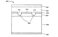
上述したように、図1の状況において、いくつかの方法では表面散乱アンテナ100は、マイクロストリップまたは平行板導波管(または複数のこのような素子)として実行され得る波伝搬構造104を含んでいる。また、これらの方法では、散乱素子は、以上で参照したD.R.Smithらの文献において提示されているような相補的メタマテリアル要素を含んでいてもよい。図5を参照すると、下部導電部または接地面502(銅または同様の物質でできている)と、誘電体基板504(デュロイド、FR4、または同様の物質でできている)と、相補的メタマテリアル要素510を組み込む上部導電体506(銅または同様の物質でできている)と、この場合は上部導電体にエッチングまたはパターン化された(例えば、PCB処理によって)成形開口部512によって規定される相補的電気LC(CELC)メタマテリアル要素とを含むマイクロストリップまたは平行板導波管の模範的なユニットセル500が示されている。
As described above, in the situation of FIG. 1, in some methods, the
図5に示されているようなCELC要素は、CELC要素の面に平行であり、またCELCギャップコンプリメントに直角である、すなわち図5の
(T.H.Handらの「相補的電界結合共鳴面の特徴づけ」Applied Physics Letters 93,212504(2008)を参照;この文献は参照によって本願に含まれる)に与えられた磁場に実質的に対応している。したがって、マイクロストリップまたは平行板導波管(図1の誘導波または表面波105の例示化である)に伝搬する誘導波の磁場素子は、
に方向づけられた磁気ダイポール励磁として実質的に特徴づけられる素子510の磁気励磁を引き起こし得る。これにより、実質的に磁気大ポール照射野である散乱電磁波を生成する。
Can cause a magnetic excitation of the
成形開口部512は、上部導電体506から電気的に絶縁されている島状導電部514をも規定するため、いくつかの方法において散乱素子は、成形開口部512の内部および/または近傍に調整材料を供給し、その後島状導電体514と上部導電体506との間にバイアス電圧を印加することによって、調整可能に構成され得る。例えば、図5に示すように、ユニットセルは液晶材料層520に沈められていてもよい。液晶は、液晶を含む分子の方向の関数である誘電率を有する。また、方向は、液晶にバイアス電圧(バイアス電界と同等)を印加することによって制御され得る。その結果、液晶は散乱素子の電磁特性の調整のための電圧整調誘電率を提供し得る。
The
液晶材料520は、例えば波伝搬構造の上面に液晶格納構造を提供することによって、散乱素子近傍に保持され得る。液晶格納構造の模範的な構成は、図5に示されている。図5は、保護部532を含み、上部導電体506と保護部532との間に分離を与える1つ以上の支持部またはスペーサ534を任意で含む液晶格納構造を表している。いくつかの方法では、液晶格納構造は、波伝搬構造の上面に接合され得る平面を有する機械加工または射出成型されたプラスチック部分である。当該平面は、散乱素子に被せられ得る1つ以上のくぼみ(例えば、溝または凹部)を含み、これらのくぼみは、例えば真空射出処理によって、液晶で満たされ得る。別の方法では、支持部534は、フォトリソグラフィック処理(例えば、米国特許第4,874,461(Satoらの「フォトリソグラフィによって形成されたスペーサを持つ液晶装置を製造するための方法」に記載されているように;この文献は参照により本願に含まれる)によって成形された球状のスペーサ(例えば、球状樹脂粒子)、壁、または柱である。保護部532を支持部534に取り付けた後、液晶の注入(例えば、真空注入)が行われる。
The
ネマチック位相液晶に関しては、分子方向は配光ベクトル場によって特徴づけられ得るものであり、物質はより大きい誘電率ε□を配光ベクトルに平行な電界構成要素に与え得、より小さい誘電率ε⊥を配光ベクトルに垂直な電界構成要素に与え得る。バイアス電圧を印加することは、成形開口部にかかるバイアス電界線をもたらし、配光ベクトルはこれらの電界線に平行に傾向となる(バイアス電圧の増加に伴って、配列角度は増加する)。これらのバイアス電界線が散乱素子の散乱励起時に生成される電界線に略平行なので、バイアス散乱素子から認められる誘電率は、対応してε□に近くなる傾向がある(すなわち、バイアス電圧の増加に対応する)。その反面、非バイアス散乱素子から認められる誘電率は、液晶の非バイアス構成に応じて決まり得る。非バイアス液晶が最大限に乱された場合(すなわち、不規則に配向された微小範囲の場合)、非バイアス散乱素子から平均誘電率εave□(ε□+ε⊥)/2を認められる。非バイアス液晶が最大限にバイアス電界線に沿って垂直に配向された場合(すなわち、バイアス電界の印加前)、非バイアス散乱素子からε⊥程小さい誘電率を認められる。その結果、散乱素子から認められる誘電率に関してより広範囲の調整を実現することが望まれる実施形態においては(散乱素子の有効静電容量のより広範囲の調整に対応し、それが故散乱素子の共鳴周波数のより広範囲の調整)、ユニットセル500は、液晶層510の上面および/または下面に配置され、印可されたバイアス電圧に対応するバイアス電界線に略垂直な方向に液晶配向ベクトルを並べるように構成された位置依存性配列層を含んでいてもよい。配列層は、例えばポリイミド層を含んでいてもよい。当該ポリイミド層は、擦り減らされる、またはパターン化される(例えば、機械加工またはフォトリソグラフィにより)ことによって、成形開口部512の導管に平行に伸びる微細な溝が設けられている。
For nematic phase liquid crystals, the molecular direction can be characterized by a light distribution vector field, and the material can give a larger dielectric constant ε □ to the electric field component parallel to the light distribution vector, and a smaller dielectric constant ε ⊥ Can be applied to the electric field component perpendicular to the light distribution vector. Applying a bias voltage results in bias field lines across the shaped aperture, and the light distribution vector tends to be parallel to these field lines (the array angle increases with increasing bias voltage). Since these bias electric field lines are substantially parallel to the electric field lines generated at the time of scattering excitation of the scattering element, the dielectric constant observed from the bias scattering element tends to be correspondingly close to ε □ (ie, the increase of the bias voltage). Corresponding to). On the other hand, the dielectric constant recognized from the non-bias scattering element can be determined according to the non-bias configuration of the liquid crystal. When the non-biased liquid crystal is disturbed to the maximum extent (that is, in the case of an irregularly oriented micro range), an average dielectric constant ε ave □ (ε □ + ε ⊥ ) / 2 is recognized from the non-bias scattering element. If a non-bias the liquid crystal is oriented vertically along the bias electric field lines to maximize (i.e., before application of the bias field) it is observed a small dielectric constant from the unbiased scattering element as epsilon ⊥. As a result, in embodiments where it is desired to achieve a wider range of adjustments with respect to the dielectric constant seen from the scattering element (corresponding to a wider range of adjustment of the effective capacitance of the scattering element, this is why the resonance of the scattering element is The
代わりにまたは加えて、ユニットセルは、成形開口部512の導管に略垂直に液晶を配向させる(例えば、上述した上部導電体506と島状導電部514との間にバイアス電圧を印加することにより)第1バイアス部、および成形開口部512の導管に略平行に液晶を配向させる(例えば、ユニットセルの四隅において上部導電体506の上に配置された電極を導入し、隣接する隅の電極に逆電圧を印加することにより)第2バイアス部を提供してもよい。散乱素子の調整は、例えば第1バイアス部と第2バイアス部との間で交互に行うか、第1および第2バイアス部の相対強度を調整することにより実現されてもよい。
Alternatively or in addition, the unit cell orients the liquid crystal substantially perpendicular to the conduit of the shaping opening 512 (eg, by applying a bias voltage between the
いくつかの方法においては、犠牲層を用いて、成形開口部512近傍により大容量の液晶を入れることによって、液晶調整の効果を向上させてもよい。この方法の図を図6に示す。図6は、図5のユニットセル500を側面から見た図を示しており、ユニットセル500には誘導体基板504と上部導電体506との間に配置された犠牲層600(例えば、ポリイミド層)がさらに設けられている。成形開口部512を規定するための、上部導電体506のエッチングに続いて、犠牲層600のさらなる選択的なエッチングにより、液晶520によって満たされ得る空洞602を生成する。いくつかの方法においては、犠牲層600の選択的なエッチングのパターンを規定するために別の遮蔽層が使われている(上部導電体506によって作成することの代わりに、または加えて)。
In some methods, the effect of liquid crystal adjustment may be improved by using a sacrificial layer and putting a large volume of liquid crystal near the forming
多様な実施形態において実施され得る模範的な液晶は、4−シアノ−4´−ペンチルビフェニル、およびLCMS−107(LC Matter)またはGT3−23001(Merck)等の高複屈折性共晶LC混合物を含んでいる。いくつかの方法では、二周波液晶を利用してもよい。二周波液晶において、配向ベクトルはより低い周波数では印加バイアス電界に略平行であり、より高い周波数では印加バイアス電界に略に垂直に並ぶ。結果的に、これらの二周波液晶を実施する方法においては、印可バイアス電圧信号の周波数を調整することによって、散乱素子の調整を実現し得る。他の方法では、一般的に液晶の弛緩/切替時間がより短い高分子網目液晶(PNLCs)またはポリマー分散液晶(PDLCs)を実施してもよい。前者の例は、ネマチックLCホスト(例えば、LCMS−107)における高分子化合物(例えば、BPA−ジメタクリレート)の熱硬化性またはUV硬化性の混合物である(Y.H.Fanらの「赤外光変調装置のための高速応答および非散乱性高分子網目液晶」Applied Physics Letters 84,1233-35(2004)を参照;この文献は参照により本願に含まれる)。後者の例は、ネマチックLC(例えば、LCMS−107)に含浸させた多孔性高分子化合物(例えば、PTEE薄膜)である(T.Kukiらの「液晶に含浸された薄膜を用いたマイクロ波可変遅延線」Microwave Symposium Digest,2002 IEEE MTT-S International,vol.1,pp.363-366(2002)参照;この文献は参照により本願に含まれる)。 Exemplary liquid crystals that can be implemented in various embodiments include 4-cyano-4′-pentylbiphenyl and high birefringent eutectic LC mixtures such as LCMS-107 (LC Matter) or GT3-23001 (Merck). Contains. In some methods, a dual frequency liquid crystal may be utilized. In a dual frequency liquid crystal, the orientation vector is substantially parallel to the applied bias electric field at lower frequencies and is aligned substantially perpendicular to the applied bias electric field at higher frequencies. As a result, in the method of implementing these two-frequency liquid crystals, adjustment of the scattering element can be realized by adjusting the frequency of the applied bias voltage signal. In other methods, polymer network liquid crystals (PNLCs) or polymer dispersed liquid crystals (PDLCs), which generally have a shorter relaxation / switching time of the liquid crystals, may be implemented. An example of the former is a thermosetting or UV curable mixture of polymer compounds (eg BPA-dimethacrylate) in a nematic LC host (eg LCMS-107) (infrared by YH Fan et al. See "Fast-response and non-scattering polymer network liquid crystals for light modulators" Applied Physics Letters 84, 1233-35 (2004); this document is hereby incorporated by reference). An example of the latter is a porous polymer compound (eg, PTEE thin film) impregnated in nematic LC (eg, LCMS-107) (T. Kuki et al., “Microwave Variable Using Thin Film Impregnated in Liquid Crystal”. Delay Line "Microwave Symposium Digest, 2002 IEEE MTT-S International, vol. 1, pp. 363-366 (2002); this document is incorporated herein by reference).
続いて、島状導電体514と上部導電体506との間にバイアス電圧を印加するための方法に関しては、上部導電体506は1つのユニットセルから次のユニットセルまで連続して伸びる。これにより、すべてのユニットセルの上部導電体への電気的接続は、マイクロストリップの上部導電体またはユニットセル500により構成される平行板導波管への単独接続によって得ることができる。島状導電体514に関して、図5はバイアス電圧線530の島状導電体への取り付け方の例を示している。この例では、バイアス電圧線530は、島状導電体の中央に取り付けられており、散乱素子の対称面に沿って当該島状電体から離れて伸びている。対称面に沿った位置合わせの効力によって、散乱素子の散乱励起時にバイアス電圧線によって生成された電界は、バイアス電圧線に略垂直であり、その結果、散乱素子の散乱特性を乱すまたは変更し得るバイアス電圧線の電流を起こさない。バイアス電圧線530は、例えば絶縁層(例えば、ポリイミド)を溶着し、島状導電体514の中央に絶縁層をエッチングし、その後バイアス電圧線530を規定する導電フィルム(例えば、クロム/金二重層)をパターン化するリフトオフ処理を用いることによって、ユニットセルに設けてもよい。
Subsequently, with respect to a method for applying a bias voltage between the island-shaped
図7A〜7Hは、表面散乱アンテナの各種の実施形態に従って使われて得る各種のCELC要素を示している。これらは、模範的な素子の概略図であり、正しい尺度で示しておらず、単に各種の実施形態に適し得る数多くのCECL素子の代表に過ぎない。図7Aは、図5において使われている素子に対応する。図7Bは、代替のCELC要素を示しており、7AのCELC要素と位相的に等しいが、素子のアームの長さを増すために波状ペリメータを使用することによって、素子の静電容量を増やしているCELC要素を示している。図7Cおよび7Dは、偏向制御を与えるために利用され得る1対の素子様式を示している。これらの直交する素子が
に配向された電磁場を有する誘導波または表面波によって励起される場合、この印可された電磁場は7Cまたは7Dそれぞれの素子の
に対して+45°または−45°に配向された磁気双極子励起として実質的に規定され得る電磁励起を引き起こす。図7Eおよび7Fは、直交したCELC要素であって、アームも+45°に傾斜されたCELC要素の変形例を示している。これらの傾斜した構成は、二極性の応答を引き起こすCELC要素の領域すべては、励磁場に直交して配向されているか(それ故励磁されない)、または当該例磁場に対して45°の方向に配向されているため、より高い磁気双極子応答を潜在的に提供する可能性がある。最後に、図7Eおよび7Fは、図7Bの波状CELC要素を同様に傾斜した変形例を示している。 Cause an electromagnetic excitation that can be substantially defined as a magnetic dipole excitation oriented at + 45 ° or -45 ° relative to. 7E and 7F show variations of CELC elements that are orthogonal CELC elements with the arms also tilted to + 45 °. These tilted configurations are such that all regions of the CELC element that cause a bipolar response are oriented perpendicular to the excitation field (and therefore not excited) or oriented in a 45 ° direction with respect to the magnetic field in question. Therefore potentially providing a higher magnetic dipole response. Finally, FIGS. 7E and 7F show a variation in which the wavy CELC element of FIG. 7B is similarly tilted.
図5には、マイクロストリップ等の波伝搬構造の上部導電体506上にパターン化されたメタマテリアル要素510の例を示しているが、別の方法では、図8に示したように、メタマテリアル要素は、マイクロストリップ自身に配置されておらず、マイクロストリップのエバネッセント近傍内(すなわち、縁領域内)に配置されている。このようにして、図8は、接地面802、誘電体基板804、上部導電体806、およびマイクロストリップの両側に沿って配置された導電ストリップ808を有するマイクロストリップの構成を示している。これらの導電ストリップ808は、成形開口部812によって規定される相補的メタマテリアル要素810を組み込んでいる。この例において、相補的メタマテリアル要素は、図7に示したような、波状ペリメータCELC要素である。図8に示したように、ビア840は、各メタマテリアル要素の島状誘電体814にバイアス電圧線830を接続するために用いられ得る。結果として、この構成は、マイクロストリップ信号トレースとメタマテリアル要素とを提供する層1、およびマイクロストリップ接地面とバイアストレースとを提供する層2を有する2層PCB処理(介在誘電体を有する2つの導電層)を使って容易に実施され得る。誘導層および導電層は、銅張Rogers5880等の高効率物質であってよい。前述したように、調整は、メタマテリアル要素810上に液晶層(不図示)を配置することによって実現されてもよい。
FIG. 5 shows an example of a
さらに別の方法では、図9Aおよび9Bに示すように、波伝搬構造は、共面導波管(CPW)であり、メタマテリアル要素は、共面導波管の束の間の近傍の中(すなわち、縁領域)に配置されている。したがって、図9Aおよび9Bは、下部接地面902、CPW信号トレース907の両側の中央接地面906、および相補的メタマテリアル要素920(1つだけ示されているが、本方法では、CPWの長さに沿って当該要素を連続して配置する)を組み込む上方接地面910を有する共面導波管の構造を示している。これらの連続する導電層は、誘電層904,908によって分離されている。共面導波管は、CPWの高位モードを断ち切る、なおかつ/あるいは隣接したCPW(不図示)間のクロストークを減らすように働くビア930の列柱によって固定されていてもよい。CPWストリップの幅909は、メタマテリアル要素920への連結を制御するために、例えば開口率を高めたり、なおかつ/あるいはビームプロファイルの開口部の傾斜を制御したりするために、CPWの長さに応じて変更し得る。CPWの間隔911は、線インピーダンス制御によって調整され得る。図9Bに示すように、第3誘電層912およびスルービア940は、各メタマテリアル要素の島状導電体922および構造の裏面に位置するバイアスパッド952に、バイアス電圧線950を接続するために使用され得る。第3誘電層912における導管924は、導電要素の成形開口部周辺に液晶(不図示)を配列させる。この構成は、4層PCB処理(3つの介在誘電層を有する4つの導電層)を使って実施され得る。これらのPCBは、電気メッキおよび無電解のメッキ技術同様、スルー、ブラインド、およびベリードビア構成と一緒に積層構造を使って製造されてもよい。
In yet another method, as shown in FIGS. 9A and 9B, the wave propagation structure is a coplanar waveguide (CPW) and the metamaterial element is in the vicinity between a bundle of coplanar waveguides (ie, Edge region). Thus, FIGS. 9A and 9B show a
図10および11に示されているさらなる別の方法では、波伝搬構造は、閉塞または管状導波管であり、メタマテリアル要素は、閉塞導波管の表面に沿って配置されている。したがって、図10は、凹部1002およびメタマテリアル要素1010を組み込む導電面1004によって規定される導波管であって、長方形状の断面を有する閉塞または管状導波管を示している。切断面図が示すように、誘電層1022を通るビア1020は、メタマテリアル要素の島状伝導1012にバイアス電圧線1030を接続するために使われ得る。凹部1002は、閉塞導波管の「床および壁」を与えるために圧延または成形される金属片として用いられ得る。そして、導波管の「天井」は、バイアストレース1030を与える上層、およびメタマテリアル要素1010を与える下層を有する2層プリント基板として用いられ得る。導波管は、メタマテリアル要素を調整するために、液晶によって満たされ得る小さい凹部1050を有する誘電体1040(例えば、PTFE)を備えていてもよい。
In yet another method shown in FIGS. 10 and 11, the wave propagation structure is a closed or tubular waveguide, and the metamaterial element is disposed along the surface of the closed waveguide. Accordingly, FIG. 10 shows a waveguide defined by a
図11に示すように、代替的な閉塞導波管の実施形態においては、長方形状の断面を有する閉塞導波管は、凹部1102および導電面1104によって規定される。ユニットセルの切断図が示すように、導電面1104は、誘導波と共振器要素1110との間を連結するアイリス1106を有する。この例において、相補的メタマテリアル要素は、図7Bに示されるような、波状ペリメータCELC要素である。図中では、長方形状の連結アイリスを示しているが、他の形状を用いてもよく、アイリスのサイズは、散乱素子への連結を制御するために(例えば、開口率を高めたり、なおかつ/あるいはビームプロファイルの開口部の傾斜を制御したりするために)、導波管の長さに応じて変更し得る。誘電層1122を通る1対のビア1120は、メタマテリアル要素の島状導電部1112にバイアス電圧線1130を接続するために、短い経路線1125と一緒に使われてもよい。凹部1102は、閉塞導波管の「床および壁」を与えるために圧延または成形される金属片として用いられ得る。そして、導波管の「天井」は、メタマテリアル要素1110(およびバイアストレース1130)を与える上層、およびアイリス1106(およびバイアス経路1125)を与える下層を有する2層プリント基板として用いられ得る。メタマテリアル要素1110は、隣接するユニットセル間の連結またはクロストークを減らすために、誘電層1122を通って伸びるビア1150の列柱によって、任意に固定され得る。前述したように、調整は、メタマテリアル要素1110上に液晶層(不図示)を配置することによって実現されてもよい。
As shown in FIG. 11, in an alternative occlusion waveguide embodiment, an occlusion waveguide having a rectangular cross-section is defined by a
図10および図11の導波管の実施形態では、単なる長方形状の断面を有している導波管を提供するが、いくつかの方法では、導波管は1つ以上のリッジ(二重リッジ導波管のように)を含んでいてもよい。リッジ導波管は、単に長方形状導波管よりも広い帯域幅を提供できる。また、リッジのジオメトリ(幅/高さ)は、散乱素子への結合部を制御するために(例えば、開口率を高めたり、なおかつ/あるいはビームプロファイルの開口部の傾斜を制御したりするために)、なおかつ/あるいはなだらかなインピーダンス変化を提供するために(例えばSMAコネクタ給電部から)、導波管の長さに応じて変動し得る。 While the waveguide embodiment of FIGS. 10 and 11 provides a waveguide having a simple rectangular cross section, in some methods, the waveguide has one or more ridges (double (Such as a ridge waveguide). Ridge waveguides can provide a wider bandwidth than simply rectangular waveguides. Also, the geometry (width / height) of the ridge is used to control the coupling to the scattering element (eg, to increase the aperture ratio and / or to control the tilt of the aperture of the beam profile). ) And / or may vary depending on the length of the waveguide to provide a gentle impedance change (eg, from an SMA connector feed).
様々な方法において、例えば、アンテナ制御回路に接続するためのパッド構造に各散乱素子のバイアス電圧線を伸ばすことによりバイアス電圧線を直接的にアドレス指定されてもよいし、例えば、行と列とによってアドレス指定可能な電圧バイアス回路に各散乱素子を提供することにより行列アドレス指定されてもよい。図12は、マイクロストリップ1202の表面における散乱素子1200の配置のために、直接アドレス指定を提供する構成例を示しており、複数のバイアス電圧線1204が散乱素子に個別のバイアス電圧を供給するためにマイクロストリップの長さ方向に沿って伸びている(代わりに、バイアス電圧線1204は、マイクロストリップに垂直に伸び、かつマイクロストリップの長さ方向に沿ってパッドまたはビアまで伸ばされていてもよい)。(図は、例えば偏向制御を与える等、散乱素子を垂直方向に配置する方法の例も示している。この場合、マイクロストリップに沿って伝搬する誘導波は、
に方向づけられた磁場を有しており、その結果、
に対して±45°の方向に向けられた磁気双極子励起として実質的に特徴づけられ得る励磁を引き起こす散乱素子の両方向に連結されていてもよい。)図13は、散乱素子1300の配置(例えば、平行板導波管の表面上)に行列アドレス指定を提供する構成例を示しており、各散乱素子は、行入力1306および列入力1308によってアドレス指定可能なバイアス回路1304に、バイアス電圧線1302を介して接続されている(各行入力および/または列入力列は1つ以上の信号を含んでおり、例えば各行または各列は単線またはその行または列に専用の1組の平行線によってアドレス指定されてもよい)。各バイアス回路は、例えばスイッチング装置(例えば、トランジスタ)、記憶装置(例えば、蓄電器)、および/または論理/多重回路、デジタル−アナログ変換回路等の付加的な回路を含んでいてもよい。この回路は、例えば薄膜トランジスタ(TFT)処理等、モノリシック集積回路を用いて素早く製造してもよいし、例えば表面実装技術(SMT)等を用いて波伝搬構造に実装された集積回路のハイブリッド型組み立て部品として素早く製造してもよい。いくつかの方法では、バイアス電圧は、ACバイアス信号の振幅を調整することによって調整されてもよい。他の方法では、バイアス電圧は、ACシグナルに対してパルス幅変調を施すことによって調整されてもよい。
May be coupled in both directions of the scattering element causing excitation, which can be substantially characterized as magnetic dipole excitation directed in the direction of ± 45 °. FIG. 13 shows an example configuration that provides matrix addressing for the arrangement of scattering elements 1300 (eg, on the surface of a parallel plate waveguide), where each scattering element is addressed by a
続いて図14を参照すると、例示的な実施形態が、システムブロック図として示されている。システム1400は、アンテナユニット1420に1つ以上の給電部1412によって連結されている通信ユニット1400を含んでいる。通信ユニット1410は、例えば携帯ブロードバンド衛星無線電話機、送信機、受信機、またはラジオあるいはマイクロ波通信システム用の無線電話機モジュールを含んでいてもよく、データ多重化/逆多重化回路、エンコーダ/デコーダ回路、モジュレータ/デモジュレータ回路、周波数アップコンバータ/ダウンコンバータ、フィルタ、増幅器、およびデュプレックス等を組み込んでいてもよい。アンテナユニットは、送信、受信、または両方を行うように構成された少なくとも1つの表面散乱アンテナを含む。また、いくつかの方法において、アンテナユニット1420は、複数の表面散乱アンテナを備えていてもよい。例えば、第1および第2の表面散乱アンテナはそれぞれ送信および受信を行うように構成されている。複数の給電部を有する表面散乱アンテナを有する実施形態においては、通信ユニットはMIMO回路を含んでいてもよい。システム1400は、アンテナの構成を決定する制御入力1432を提供するように構成されたアンテナ制御部1430を含んでいてもよい。例えば、制御入力は、各散乱素子への入力(例えば、図12に示したような直接アドレス指定設定)、行入力および列入力(例えば、図13に示したような行列アドレス指定設定)、およびアンテナ給電部のための調整ゲイン等を備えていてもよい。
With continued reference to FIG. 14, an exemplary embodiment is shown as a system block diagram.
いくつかの方法では、アンテナ制御部1430は、アンテナの環境条件(例えば、その位置、方向、温度、および機械的変形等)を検出するセンサ部材を持つセンサユニットを任意で含んでいる。例えば、アンテナ制御部1430は、1組の所望のアンテナ照射パターン(本開示内で上述したビーム方向、ビーム幅、および配向状態等に対応)に対応する、制御入力1432のための1組の値を割り出すルックアップテーブル等として、1組の表面散乱アンテナ構成を備えていてもよい。このルックアップテーブルは、
制御入力の値の範囲に対して、アンテナの全波シミュレーションを実行したり、アンテナを試験環境下に配置して制御入力の値の範囲に対応するアンテナ照射パターンを測定したりする等して、予め算出されていてもよい。いくつかの方法では、アンテナ制御部は、上記のルックアップテーブルを用いて、回帰分析に応じた制御入力を算出するように構成されていてもよい。具体的には、例えば上記のルックアップテーブル内に格納されている2つのアンテナ照射パターン間の制御入力に対する値を補間する(例えば、ルックアップテーブルがビームステアリング方向の離散的インクリメントのみを含む場合に、連続的なビームステアリングを可能にするため)ことにより、制御入力を算出してもよい。あるいは、アンテナ制御部1430は、選択されたあるいは所望のアンテナ照射パターンに対応する制御入力1432を動的に算出するように構成されていてもよい。具体的には、例えば干渉項Re[ΨoutΨ* in]に対応するホログラフィックパターンを算出したり(本開示内で上述したとおり)、選択されたあるいは所望のアンテナ照射パターンを提供するカップリング{αj}(制御入力の値に対応)を本開示内で提示した式(1)に基づいて算出したりすることにより、制御入力1432を算出してもよい。
In some methods, the
Perform a full-wave simulation of the antenna for the control input value range, or place the antenna in the test environment and measure the antenna irradiation pattern corresponding to the control input value range, etc. It may be calculated in advance. In some methods, the antenna control unit may be configured to calculate a control input corresponding to the regression analysis using the lookup table. Specifically, for example, a value for a control input between two antenna irradiation patterns stored in the above lookup table is interpolated (for example, when the lookup table includes only discrete increments in the beam steering direction). The control input may be calculated by enabling continuous beam steering. Alternatively, the
いくつかの方法では、アンテナユニット1420は、アンテナの環境条件(例えば、その位置、方向、温度、および機械的変形等)を検出するセンサ部材を任意で含んでいる。センサ部材は、GPS装置、ジャイロスコープ、温度計、および歪みゲージ等を1つ以上含んでいてもよい。また、センサユニットは、センサデータ1424をアンテナ制御部に提供するために、当該アンテナ制御部に接続されていてもよい。これにより、アンテナの移動または回転(例えば、アンテナが航空機等の通信プラットフォームに搭載されている場合)、あるいは温度ドリフト、機械的変形等を補正するために制御入力1432を調整してもよい。
In some methods, the
いくつかの方法では、通信ユニットは、制御入力のフィードバック調整のために、フィードバック信号1434をアンテナ制御部に提供してもよい。例えば、通信ユニットは、ビットエラーレート信号を提供し、アンテナ制御部は、チャンネルノイズを軽減するためにアンテナ構成を調整するフィードバック回路(例えば、DSP回路)を含んでいてもよい。あるいは/さらに、ポインティングアプリケーションあるいはステアリングアプリケーションのために、アンテナ制御部はフィードバック回路(例えば、通信ブロードバンド衛星放送の受信機のためのポインティングロックDSP回路)を含んでいてもよい。
In some methods, the communication unit may provide a
説明のための実施形態が、処理フロー図として図15に図示されている。フロー1500は、表面散乱アンテナのための第1アンテナ照射パターンであって、1つ以上の制御入力に変動的に対応する第1アンテナ照射パターンを選択する工程1510を含む。例えば、通信衛星、通信基地局、あるいは通信モバイルプラットフォームの位置において、照射パターンの一次ビームを方向づけるようなアンテナ照射パターンが選択される。あるいは/さらに、所望の位置に照射パターンのヌルを位置づけるようなアンテナ照射パターンが選択される(例えば、通信を確実にするため、あるいはノイズ源を取り除くため)。あるいは/さらに、円偏向(例えば、Ka帯衛星通信)または直線偏向(例えば、Ku帯衛星通信)等、所望の偏向状態を提供するようなアンテナ照射パターンが選択される。フロー1500は、選択された第1アンテナ照射パターンに対応する1つ以上の制御入力の第1値を決定する工程1520を含む。例えば、図14に示すシステムでは、アンテナ制御部1430は、ルックアップテーブルを用いることによって、あるいは所望のアンテナ照射パターンに対応するホログラムを算出することによって、制御入力の値を決定するように構成された回路を含んでいてもよい。フロー1500は、表面散乱アンテナのための1つ以上の制御入力の第1値を提供する工程1530を任意で含む。例えば、アンテナ制御部1430は、種々の散乱素子にバイアス電圧を印加することが可能であり、なおかつ/あるいはアンテナ制御部1430は、アンテナ給電部のゲインを調整することが可能である。フロー1500は、第1アンテナ照射パターンとは異なる第2アンテナ照射パターンを選択する工程1540を含む。本工程も同様に、例えば第2ビーム方向あるいはヌルの第2位置を選択する工程を含み得る。この方法の一適用例では、衛星通信ターミナルは、複数の衛星間で切り替わることができる。例えば、最大負荷時に容量を最適化するために切り替わったり、使用が開始された他の衛星に切り替わったり、あるいは使用が終了した最初の衛星またはオフラインの最初の衛星から切り替わったりすることができる。フロー1500は、選択された第2アンテナ照射パターンに対応する1つ以上の制御入力の第2値を決定する工程1550を含む。本工程も同様に、例えばルックアップテーブルを用いたり、ホログラフィックパターンを算出したりし得る。フロー1500は、表面散乱アンテナのための1つ以上の制御入力の第2値を提供する工程1560を任意で含む。本工程も同様に、例えば、倍す電圧を印加し、なおかつ/あるいは給電ゲインを調整する工程を含み得る。
An illustrative embodiment is illustrated in FIG. 15 as a process flow diagram.
説明のための他の実施形態が、処理フロー図として図16に図示されている。フロー1600は、1つ以上の第1制御入力に対応する第1変動照射パターンを有する第1表面散乱アンテナのための第1対象物を特定する工程1610を含む。この第1対象物は、例えば通信衛星、通信基地局、あるいは通信モバイルプラットフォームである。フロー1600は、第1対象物と第1表面散乱アンテナとの間の第1相対運動に対応する第1変動照射パターンの実質的な連続変異を提供するために、1つ以上の第1制御入力を繰り返し調整する工程1620を含む。例えば、図14に示したシステムでは、アンテナ制御部1430は、例えば非静止衛星を追跡するため、モバイルプラットフォーム(例えば、航空機または他の乗り物)と静止衛星とのポインティングロックを保持するため、あるいは対象物およびアンテナの両方が動く場合に、両者のポインティングロックを保持するために、表面散乱アンテナの照射パターンを方向づけるように構成された回路を含み得る。フロー1600は、1つ以上の第2制御入力に対応する第2変動照射パターンを持つ第2表面散乱アンテナのための第2対象物を特定する工程1630を任意で含む。また、フロー1600は、第2対象物と第2表面散乱アンテナとの間の第2相対運動に対応する第2変動照射パターンの実質的な連続変異を提供するために、1つ以上の第2制御入力を繰り返し調整する工程1640を任意で含む。例えば、いくつかの適用例では、第1対象物(例えば、第1非静止衛星)を追跡する第1アンテナユニットと、第2対象物(例えば、第2非静止衛星)を追跡する第2または予備アンテナユニットとの両方を配置し得る。いくつかの方法では、予備アンテナユニットは、第2対象物を追跡するために(さらには、低減したサービスの質(QoS)において第2対象物へのリンクを任意で確保するために)、最初に用いられる小開口アンテナ(txおよび/またはrx)を含んでいてもよい。フロー1600は、第1変動照射パターンの最初のビーム内に第2対象物を実質的に配置するために、1つ以上の第1制御入力を調整する工程1650を任意で含む。例えば、第1アンテナおよび第2アンテナが、非静止衛星のコンステレーションと相互作用する衛星通信ターミナルの構成部材である場合の適用例においては、第1または最初のアンテナは、衛星コンステレーションの第1部材が水平線に到達するまで(あるいは、第1アンテナが明らかなスキャンロスに陥るまで)、当該第1部材を追跡してもよい。この際、第1アンテナに衛星コンステレーションの第2部材(第2または予備アンテナによって追跡されていたもの)を追跡させることにより、「ハンドオフ」が実行される。フロー1600は、第1対象物および第2対象物とは異なる、第2表面散乱アンテナのための新たな対象物を特定する工程1660と、第2変動照射パターンの最初のビーム内に新たな対象物を実質的に配置するために、1つ以上の第2制御入力を調整する工程1670とを任意で含む。例えば、「ハンドオフ」が実行された後、第2または予備アンテナは、衛星コンステレーションの第3部材とのリンクを開始してもよい(例えば、水平線を超えて上昇した場合)。
Another illustrative embodiment is illustrated in FIG. 16 as a process flow diagram. The
上述の詳細な説明では、ブロック図、フローチャート、および/または実施例を用いて、装置および/または処理の様々な実施形態について説明した。これらのブロック図、フローチャート、および/または実施例が、1つ以上の機能および/または処理を含んでいる場合、これらブロック図、フローチャート、または実施例内の各機能および/または処理が、広範囲のハードウェア、ソフトウェア、ファームウェア、あるいはこれらの実質的な任意の組み合わせによって、個々におよび/または組み合わせで実施できることについて、当業者であれば理解するであろう。一実施形態では、本開示において示す構成要素の一部は、特定用途向け集積回路(ASIC)、フィールドプログラマブルゲートアレイ(FPGA)、デジタル信号プロセッサ(DSP)、あるいはその他の統合的な形式によって実施することができる。しかし、本開示において示す実施形態の一部の形態は、全体的あるいは部分的に、1つ以上のコンピュータにおいて実行される1つ以上のコンピュータプログラム(例えば、1つ以上のコンピュータシステムにおいて実行される1つ以上のプログラム)、1つ以上のプロセッサにおいて実行される1つ以上のプログラム(例えば、1つ以上のマイクロプロセッサにおいて実行される1つ以上のプログラム)、ファームウェア、あるいはこれらの実質的な任意の組み合わせとして、集積回路内において同等に実施することができることについて、当業者であれば認識するであろう。また、回路設計および/または上記ソフトウェアおよび/またはファームウェアへの符号の書き込みは、当業者の技術範囲内において本開示が十分に行われていることについて、当業者であれば認識するであろう。さらに、本開示において示す構成要素のメカニズムは、プログラムプロダクトとして様々な形式で分配することができ、本開示において示す構成要素の実施形態は、上記分配を実施するために実際に用いられる信号を有する媒体の種類に関わらず適用されることについて、当業者であれば理解するであろう。信号を有する媒体の例としては、記録型の媒体(例えば、フロッピー(登録商標)ディスク、ハードディスクドライブ、コンパクトディスク(CD)、デジタルビデオデスク(DVD)、デジタルテープ、コンピュータメモリ等)、および伝送型の媒体(例えば、デジタルおよび/またはアナログ通信媒体(例えば、光ファイバーケーブル、導波管、有線通信リンク、無線通信リンク(例えば、トランスミッター、レシーバー、送信論理操作、受信論理操作等))が含まれるが、これらに限定されるものではない。 In the foregoing detailed description, various embodiments of devices and / or processes have been described using block diagrams, flowcharts, and / or examples. Where these block diagrams, flowcharts, and / or examples include one or more functions and / or processes, each function and / or process within these block diagrams, flowcharts, or examples may have a wide range of Those skilled in the art will appreciate that they can be implemented individually and / or in combination by hardware, software, firmware, or virtually any combination thereof. In one embodiment, some of the components shown in this disclosure are implemented by an application specific integrated circuit (ASIC), a field programmable gate array (FPGA), a digital signal processor (DSP), or other integrated form. be able to. However, some forms of embodiments presented in this disclosure may be executed in whole or in part on one or more computer programs (eg, executed on one or more computer systems) executed on one or more computers. One or more programs), one or more programs executed on one or more processors (eg, one or more programs executed on one or more microprocessors), firmware, or substantially any of these Those skilled in the art will recognize that the combination can be equally implemented in an integrated circuit. Further, those skilled in the art will recognize that the circuit design and / or the writing of codes into the software and / or firmware is well within the technical scope of those skilled in the art. Furthermore, the component mechanisms shown in this disclosure can be distributed in various forms as program products, and the component embodiments shown in this disclosure have signals that are actually used to implement the distribution. One skilled in the art will understand that it applies regardless of the type of media. Examples of media having signals include recording media (eg, floppy (registered trademark) disk, hard disk drive, compact disk (CD), digital video desk (DVD), digital tape, computer memory, etc.), and transmission type. Media (eg, digital and / or analog communication media (eg, fiber optic cables, waveguides, wired communication links, wireless communication links (eg, transmitters, receivers, transmit logic operations, receive logic operations, etc.)). However, it is not limited to these.
一般的な意味で、当業者であれば、広範囲のハードウェア、ソフトウェア、ファームウェア、および/または実質的なこれらの任意の組み合わせによって、個別的および/または集合的に実行可能である、本書内に記載された各種実施形態が、種々のタイプの「電気回路」によって構成されていると見なされ得ることは理解できるであろう。その結果、ここで使用しているように、「電気回路」の例としては、少なくとも1つの離散型電気回路を有する電気回路、少なくとも1つの特定用途向け集積回路を有する電気回路、コンピュータプログラムによって構成される汎用演算デバイスを形成する電気回路(例えば、本書内に記載された処理および/または装置を少なくとも部分的に実行するコンピュータプログラムによって構成される汎用コンピュータ、またはここに記載される処理および/または装置を少なくとも部分的に実行するコンピュータプログラムによって構成されるマイクロプロセッサ)、メモリデバイスを形成する電気回路(例えば、RAM)、および/または通信デバイスを形成する電気回路(例えば、モデム、通信スイッチ、光電気的設備等)等が挙げられるが、これらの例に限定されるものではない。当業者ならば、本書内に記載の主題がアナログまたはデジタルの手法もしくはこれらのいくつかの組み合わせによって実行され得ることを認識するであろう。 In a general sense, those skilled in the art will understand that within this document, which can be performed individually and / or collectively by a wide range of hardware, software, firmware, and / or virtually any combination thereof. It will be appreciated that the various described embodiments may be considered as being constituted by various types of “electrical circuits”. As a result, as used herein, examples of “electrical circuits” include an electric circuit having at least one discrete electric circuit, an electric circuit having at least one application specific integrated circuit, and a computer program. Electrical circuits that form a general purpose computing device (eg, a general purpose computer configured by a computer program that at least partially executes the processes and / or apparatus described herein, or processes and / or described herein) A microprocessor configured by a computer program that at least partially executes the apparatus), an electrical circuit (eg, RAM) forming a memory device, and / or an electrical circuit (eg, modem, communication switch, optical) forming a communication device Electrical equipment etc.) , It is not limited to these examples. Those skilled in the art will recognize that the subject matter described herein can be implemented by analog or digital techniques or some combination thereof.
本明細書で参照され、なおかつ/あるいは任意の出願データシート(インサートリストを含むが、これに限定されない)にて列挙された、上記米国特許、米国特許出願公開公報、米国特許出願、外国特許、外国特許出願、並びに非特許刊行物はすべて、矛盾しない範囲で参照によってここに援用される。 US patents, US patent application publications, US patent applications, foreign patents, referred to herein and / or listed in any application data sheet (including but not limited to insert lists), All foreign patent applications, as well as non-patent publications, are hereby incorporated by reference to the extent they do not conflict.
当業者は、ここで述べた要素(例えば工程)、装置、対象物およびそれらに付随する議論が、概念の明瞭化の目的の例として用いられ、なおかつ種々の構成の修飾が検討されることを理解するだろう。したがって、ここで用いられるように、上述した具体例および付随する議論は、より一般的なクラスの代表を意図する。一般に、特定の例の使用は、そのクラスの代表であることが意図され、特定の要素(例えば動作)、装置および対象物を盛り込んでいないことは、制限的であると捉えるべきではない。 Those skilled in the art will recognize that the elements (eg, processes), devices, objects, and accompanying discussions described herein are used as examples for purposes of clarification of concepts and that various modifications of the configuration are contemplated. Will understand. Thus, as used herein, the above examples and accompanying discussion are intended to represent a more general class. In general, the use of a particular example is intended to be representative of that class, and the absence of particular elements (eg, operations), devices, and objects should not be considered limiting.
ここにある実質的な任意の複数形および/または単数形の用語について、当業者は、文脈および/または出願に最適になるように、複数形から単数形へ、および/または単数形から複数形へ変換し得る。様々な単数形/複数形の置換は、分かりやすくするためにここには明示していない。 For substantially any plural and / or singular terms herein, one of ordinary skill in the art will recognize the plural and singular and / or singular to plural as best suited to the context and / or application. Can be converted to The various singular / plural permutations are not explicitly shown here for the sake of clarity.
本書に記載の本主題に係る特定の態様を図示ならびに説明したが、本書の教示に基づけば、本書に記載の主題およびその幅広い態様から逸脱しない範囲で変更および補正がなされてもよいことは、当業者にとって明白である。それ故、このような変更および補正のすべてが本書に記載の主題の真の精神および範疇にあるように、添付の特許請求の範囲がその範疇においてこのような変更および補正のすべてを包括する。さらに、本発明は添付の特許請求の範囲によって規定される。一般に、当業者ならば、本書および特に添付の特許請求の範囲(例えば、添付の特許請求の範囲の要部)にて用いられている用語は、一般に「非限定的な」用語として意図されている(例えば、「…を含んでいる」という用語は「…を含んでいるがこれに限定されない」と解釈されるべきであり、「…を有している」という用語は「少なくとも…を有している」と解釈されるべきであり、「…を含む」という用語は「…を含むがこれに限定されない」と解釈されるべきである等)ことを理解するであろう。当業者であれば、導入された請求項の記載において特定の数が意図される場合、そのような意図は当該請求項の中に明確に記載され、そのような記載がない場合は、そのような意図も存在しないことをさらに理解するであろう。例えば、理解を促すために、後続の添付の特許請求の範囲には、請求項の記載を導入するために、「少なくとも1つの」および「1つ以上の」といった導入句の使用が含まれてもよい。しかしながら、このような句の使用により、“a”または“an”といった不定冠詞により請求項の記載を導入した場合に、たとえ同一の請求項に「1つ以上の」または「少なくとも1つの」といった導入句と“a”または“an”といった不定冠詞との両方が含まれるとしても、このような導入された請求項の記載を含んだいずれの特定の請求項も、このような記載を1つしか含まない発明に限定されると示唆されるように解釈されるべきではない(例えば、“a”および/または“an”は、「少なくとも1つの」または「1つ以上の」を意味するように典型的に解釈されるべきである)。定冠詞を使用して請求項の記載を導入する場合にも、同様のことが当てはまる。また、導入された請求項の記載において特定の数が明確に明記されている場合であっても、当業者であれば、このような記載は少なくとも記載された数を意味するように解釈されるべきであることを認識するであろう(例えば、他に修飾語を伴わない「2つの記載」という単なる記載は、少なくとも2つの記載または2つ以上の記載を典型的に意味する)。さらに、「A、B、およびC等の内の少なくとも1つ」に類する従来技法が使用される場合、一般にこのような構成は、当業者がその従来技法を理解するであろう意味において意図されている(例えば、「A、B、およびCの内の少なくとも1つを有するシステム」は、Aのみ、Bのみ、Cのみ、AとBとの両方、AとCとの両方、BとCとの両方、および/またはAとBとCとのすべて等を有するシステムを含むがこれに限定されない)。「A、B、およびC等の内の少なくとも1つ」に類する表記が使用される場合、一般にこのような構成は、当業者がその表記を理解するであろう意味において意図されている(例えば、「A、B、およびCの内の少なくとも1つを有するシステム」は、Aのみ、Bのみ、Cのみ、AとBとの両方、AとCとの両方、BとCとの両方、および/またはAとBとCとのすべて等を有するシステムを含むがこれに限定されない)。当業者であれば、2つ以上選択可能な用語を表している実質的にいずれの離接語および/または離接句も、詳細な説明、特許請求の範囲、または図面において、これらの用語の1つ、これらの用語のいずれか、またはこれらの用語の両方を含む可能性を意図するように理解されるべきであることをさらに理解するであろう。例えば、「AまたはB」という句は、「A」、「B」、または「AおよびB」の可能性を含むことが理解されるであろう。 While particular aspects of the subject matter described and illustrated herein have been illustrated and described, modifications and amendments may be made based on the teachings herein without departing from the subject matter described herein and its broad aspects. It will be obvious to those skilled in the art. Accordingly, the appended claims encompass all such changes and modifications in their scope, as all such changes and modifications are within the true spirit and scope of the subject matter described herein. Furthermore, the invention is defined by the appended claims. In general, those skilled in the art will recognize that the terms used in this document and particularly the appended claims (eg, key portions of the appended claims) are generally intended as “non-limiting” terms. (For example, the term “comprising…” should be interpreted as “including but not limited to” and the term “comprising ...” has “at least ...” It should be understood that the term “including” should be interpreted as “including but not limited to” etc.). A person skilled in the art will clearly state in the claim that such intent is explicitly stated in the claim that is introduced, and if there is no such description, It will be further understood that no intent exists. For example, to facilitate understanding, the following appended claims include the use of introductory phrases such as “at least one” and “one or more” to introduce claim recitations. Also good. However, the use of such phrases, such as “one or more” or “at least one” in the same claim, when a claim statement is introduced by an indefinite article such as “a” or “an”. Any particular claim, including a statement of such an introduced claim, should include one such statement, even if both the introductory phrase and the indefinite article such as “a” or “an” are included. Should not be construed as implied to be limited to inventions containing only (eg, “a” and / or “an” shall mean “at least one” or “one or more”. Should be typically interpreted). The same applies to the introduction of claim statements using definite articles. Further, even if a specific number is clearly specified in the description of an introduced claim, such description should be interpreted to mean at least the number described by those skilled in the art. It will be appreciated that (for example, the mere description of “two descriptions” without other modifiers typically means at least two descriptions or more than one description). Further, when a conventional technique similar to “at least one of A, B, and C, etc.” is used, such a configuration is generally intended in the sense that those skilled in the art will understand the conventional technique. (Eg, “a system having at least one of A, B, and C” includes A only, B only, C only, both A and B, both A and C, B and C And / or a system having all of A, B, C, etc.). Where a notation similar to “at least one of A, B, and C, etc.” is used, such a configuration is generally intended in the sense that those skilled in the art will understand the notation (eg, , “A system having at least one of A, B, and C” includes A only, B only, C only, both A and B, both A and C, both B and C, And / or including but not limited to systems having all of A, B, C, etc.). Those skilled in the art will recognize that substantially any disjunctive word and / or disjunctive phrase representing two or more selectable terms may be used in the detailed description, claims, or drawings. It will be further understood that one should be understood to contemplate the possibility of including one, any of these terms, or both of these terms. For example, it will be understood that the phrase “A or B” includes the possibilities of “A”, “B”, or “A and B”.
添付の特許請求の範囲に関して、当業者であれば、請求項中に記載の工程は、一般に任意の順序で実施しても構わないことが理解できるであろう。また、様々な工程の流れが一連の流れとして提示されているが、この様々な工程が、図示された順序とは他の順序で実施されても、または同時に実施されても構わないことを理解されたい。このような別の順序の例には、文脈と矛盾しない限りにおいて、繰り返し、交互に実施、中断、順序を変更、増分、準備、補充、同時、逆、またはその他の種々の順序が含まれてもよい。さらに、「…に対応した」および「…に関連した」等の用語、または他の過去時制の形容詞は、特に断りがない限り一般的にそのような変化形を排除することを意図しているわけではない。 With respect to the appended claims, those skilled in the art will appreciate that the steps recited in the claims may generally be performed in any order. Also, although the various process flows are presented as a series of flows, it is understood that the various processes may be performed in an order other than the illustrated order, or may be performed simultaneously. I want to be. Examples of such other sequences include repeated, alternating, interrupted, reordered, incremental, prepared, replenished, simultaneous, reversed, or various other orders, unless otherwise contradicted by context. Also good. In addition, terms such as "corresponding to ..." and "related to ..." or other past tense adjectives are generally intended to exclude such variations unless otherwise noted. Do not mean.
本明細書において様々な態様および実施形態が開示されてきたが、当業者であれば、他の態様および実施形態も明白である。以下の特許請求の範囲により示されている真の範疇および精神を伴いながら、本書に開示されている様々な態様および実施形態は、説明のためのものであり、限定的であるように意図されているものではない。 While various aspects and embodiments have been disclosed herein, other aspects and embodiments will be apparent to those skilled in the art. The various aspects and embodiments disclosed herein are intended to be illustrative and limiting, with the true scope and spirit indicated by the following claims. It is not what you have.
〔まとめ〕
本発明に係るアンテナ、方法およびシステムは、以下のように表現することもできる。(1)波伝搬構造と、
上記波伝搬構造に沿って配置された複数の散乱素子とを備えたアンテナであり、
上記複数の散乱素子は、
素子間の間隔が、上記アンテナの動作周波数に対応する自由空間波長よりも実質的に小さく、
上記波伝搬構造の誘導波モードあるいは表面波モードに対する複数の独立した変動電磁応答を有しており、
上記複数の独立した変動電磁応答は、上記アンテナの変動照射野を提供することを特徴とするアンテナ。
(2)上記複数の散乱素子は、複数の略同一の散乱素子であることを特徴とする(1)に記載のアンテナ。
(3)上記複数の独立した変動電磁応答は、上記波伝搬構造の上記誘導波モードあるいは上記表面波モードに対する有効媒質応答を提供することを特徴とする(1)に記載のアンテナ。
(4)上記複数の独立した変動電磁応答は、複数の磁気双極子照射野であることを特徴とする(1)に記載のアンテナ。
(5)上記動作周波数は、マイクロ波周波数であることを特徴とする(1)に記載のアンテナ。
(6)上記マイクロ波周波数は、Ka帯周波数であることを特徴とする(5)に記載のアンテナ。
(7)上記マイクロ波周波数は、Ku帯周波数であることを特徴とする(5)に記載のアンテナ。
(8)上記マイクロ波周波数は、Q帯周波数であることを特徴とする(5)に記載のアンテナ。
(9)上記素子間の間隔は、上記自由空間波長の4分の1の長さよりも小さいことを特徴とする(1)に記載のアンテナ。
(10)上記素子間の間隔は、上記自由空間波長の5分の1の長さよりも小さいことを特徴とする(1)に記載のアンテナ。
(11)上記波伝搬構造は、1つ以上の導電面と、当該1つ以上の導電面内の複数の開口部に対応する上記複数の散乱素子とを含むことを特徴とする(1)に記載のアンテナ。
(12)
上記波伝搬構造は、略二次元の波伝搬構造であることを特徴とする(11)に記載のアンテナ。
(13)上記略二次元の波伝搬構造は、平行板導波管であり、
上記1つ以上の導電面は、上記平行板導波管の上部導電体であることを特徴とする(12)に記載のアンテナ。
(14)上記波伝搬構造は、1つ以上の略一次元の波伝搬構造を含むことを特徴とする(11)に記載のアンテナ。
(15)上記1つ以上の略一次元の波伝搬構造は、略二次元のアンテナ領域を構成する複数の略一次元の波伝搬構造であることを特徴とする(14)に記載のアンテナ。
(16)上記1つ以上の略一次元の波伝搬構造は、1つ以上のマイクロストリップを含むことを特徴とする(14)に記載のアンテナ。
(17)上記1つ以上の導電面は、上記1つ以上のマイクロストリップ各々の1つ以上の上部導電体であることを特徴とする(16)に記載のアンテナ。
(18)上記1つ以上の導電面は、上記1つ以上のマイクロストリップの1つ以上の上部導電体に平行に配置された1つ以上の導電ストリップであることを特徴とする(16)に記載のアンテナ。
(19)上記1つ以上の略一次元の波伝搬構造は、1つ以上の共面導波管を含むことを特徴とする(14)に記載のアンテナ。
(20)上記1つ以上の導電面は、上記1つ以上の共面導波管の上に配置されていることを特徴とする(19)に記載のアンテナ。
(21)上記1つ以上の略一次元の波伝搬構造は、1つ以上の閉塞導波管を含むことを特徴とする(14)の記載のアンテナ。
(22)上記1つ以上の閉塞導波管は、1つ以上の長方形導波管を含むことを特徴とする(21)に記載のアンテナ。
(23)上記1つ以上の長方形導波管は、1つ以上の二重リッジの長方形導波管を含むことを特徴とする(22)に記載のアンテナ。
(24)上記1つ以上の導電面は、上記1つ以上の閉塞導波管各々の1つ以上の上面であることを特徴とする(21)に記載のアンテナ。
(25)上記1つ以上の導電面は、上記1つ以上の閉塞導波管各々の1つ以上の上面上に配置されており、
上記1つ以上の上面は、上記1つ以上の導電面内の上記複数の開口部に隣接した複数のアイリスを含むことを特徴とする(21)に記載のアンテナ。
(26)上記複数の開口部は、上記1つ以上の導電面と電気的に絶縁された複数の島状導電部各々を規定し、
上記アンテナは、
上記1つ以上の導電面と上記複数の島状導電部各々との間それぞれに、バイアス電圧を印加するように構成された複数のバイアス電圧線と、
上記複数の開口部の周辺に少なくとも部分的に配置された電気的調整材料とをさらに備えることを特徴とする(11)に記載のアンテナ。
(27)上記電気的調整材料は、液晶材料であることを特徴とする(26)に記載のアンテナ。
(28)上記液晶材料は、ネマチック液晶であることを特徴とする(27)に記載のアンテナ。
(29)上記液晶材料は、二周波液晶であることを特徴とする(27)に記載のアンテナ。
(30)上記液晶材料は、高分子網目液晶であることを特徴とする(27)に記載のアンテナ。
(31)上記液晶材料は、高分子分散液晶であることを特徴とする(27)に記載のアンテナ。
(32)上記複数の開口部は、上記1つ以上の導電面と電気的に絶縁された複数の島状
導電部各々を規定し、行列状に配置されており、
上記アンテナは、
上記1つ以上の導電面と上記複数の島状導電部各々との間それぞれに、バイアス電圧を印加するように構成された複数のバイアス回路と、
上記複数のバイアス回路の列を各々がアドレス指定する1組の列制御線と、
上記複数のバイアス回路の行を各々がアドレス指定する1組の行制御線と、
上記複数の開口部の周辺に少なくとも部分的に配置された電気的調整材料とをさらに備えることを特徴とする(11)に記載のアンテナ。
(33)上記複数のバイアス回路各々は、上記複数の開口部に隣接する位置に行列状に配置されていることを特徴とする(32)に記載のアンテナ。
(34)上記複数の開口部は、上記誘導波あるいは上記表面波の磁場に対する複数の磁気双極子応答を有する複数の相補的メタマテリアル要素を規定することを特徴とする(11)に記載のアンテナ。
(35)上記複数の相補的メタマテリアル要素は、複数の相補的電気LCメタマテリアル要素であることを特徴とする(34)に記載のアンテナ。
(36)上記複数の磁気双極子応答は、上記1つ以上の導電面に平行に方向づけられた複数の面内磁気双極子応答であることを特徴とする(34)に記載のアンテナ。
(37)上記複数の面内磁気双極子応答は、上記1つ以上の導電面に平行な第1方向に方向づけられた複数の第1面内磁気双極子と、上記第1方向に垂直であり、かつ、上記1つ以上の導電面に平行な第2方向に方向づけられた複数の第2面内磁気双極子とを含むことを特徴とする(36)に記載のアンテナ。
(38)対応する複数の第1位相を複数の位置各々に届けるための第1誘導波あるいは表面波を伝搬する工程と、
複数の位置各々の中から選択された第1組の位置で上記第1誘導波あるいは表面波に結合させ、当該第1組の位置で第1照射野を生成する複数の第1電磁振動を生じさせる工程と、
上記複数の第1位相と略同等であり、対応する複数の第2位相を上記複数の位置各々に届けるための第2誘導波あるいは表面波を伝搬する工程と、
複数の位置各々の中から選択された第2組の位置で上記第2誘導波あるいは表面波に結合させ、当該第2組の位置で第1照射野とは異なる第2照射野を生成する複数の第2電磁振動を生じさせる工程とを含むことを特徴とする方法。
(39)上記第1誘導波あるいは表面波、および上記第1照射野は、第1干渉縞を規定し、上記複数の位置各々の中から選択された上記第1組の位置は、上記第1干渉縞の建設的干渉領域内の1組の位置に対応し、
上記第2誘導波あるいは表面波、および上記第2照射野は、上記第1干渉縞とは異なる第2干渉縞を規定し、上記複数の位置各々の中から選択された上記第2組の位置は、上記第2干渉縞の建設的干渉領域内の1組の位置に対応することを特徴とする(38)に記載の方法。
(40)複数の位置で第1自由空間波を受け取る工程と、
複数の位置各々の中から選択された第1組の位置で上記第1自由空間波に結合させ、対応する複数の第1位相を有する第1誘導波あるいは表面波を上記複数の位置で生成する複数の第1電磁振動を当該第1組の位置で生じさせる工程と、
複数の位置で第1自由空間波とは異なる第2自由空間波を受け取る工程と、
複数の位置各々の中から選択された第2組の位置で上記第2自由空間波に結合させ、複数の第1位相と略同等であり、対応する複数の第2位相を有する第2誘導波あるいは表面波を上記複数の位置で生成する複数の第2電磁振動を当該第2組の位置で生じさせる工程とを含むことを特徴とする方法。
(41)上記第1誘導波あるいは表面波、および上記第1自由空間波は、第1干渉縞を規定し、上記複数の位置各々の中から選択された上記第1組の位置は、上記第1干渉縞の建設的干渉領域内の1組の位置に対応し、
上記第2誘導波あるいは表面波、および上記第2自由空間波は、上記第1干渉縞とは異なる第2干渉縞を規定し、上記複数の位置各々の中から選択された上記第2組の位置は、上記第2干渉縞の建設的干渉領域内の1組の位置に対応することを特徴とする(40)に記載の方法。
(42)第1アンテナ照射パターンを選択する工程と、
1つ以上の制御入力に対して変動的に応答する表面散乱アンテナについて、選択された上記第1アンテナ照射パターンに対応する上記1つ以上の制御入力の第1値を決定する工程とを含むことを特徴とする方法。
(43)上記表面散乱アンテナは、上記1つ以上の制御入力の機能である変動物理パラメータを各々が有する複数の散乱素子を有していることを特徴とする(42)に記載の方法。
(44)上記1つ以上の制御入力の第1値を決定する工程は、
選択された上記第1アンテナ放射パターンを提供するために、各上記変動物理パラメータの各々の第1値を決定する工程と、
各上記変動物理パラメータに関して決定された上記各々の第1値に対応する上記1つ以上の制御入力の上記第1値を決定する工程とを含むことを特徴とする(43)に記載の方法。
(45)各上記変動物理パラメータは、上記複数の散乱素子の各変動共振周波数であることを特徴とする(43)に記載の方法。
(46)上記1つ以上の制御入力は、上記複数の散乱素子のための複数のバイアス電圧各々を含むことを特徴とする(43)に記載の方法。
(47)上記複数の散乱素子は、列および行によってアドレス指定可能であり、
上記1つ以上の制御入力は、1組の列入力部および1組の行入力部を含むことを特徴とする(43)に記載の方法。
(48)上記複数の散乱素子は、調整ゲインを有する1組の給電線によって給電され、
上記1つ以上の制御入力は、上記調整ゲインを含むことを特徴とする(43)に記載の方法。
(49)上記表面散乱アンテナのための上記1つ以上の制御入力の上記第1値を提供する工程をさらに含むことを特徴とする(43)に記載の方法。
(50)上記第1アンテナ照射パターンを選択する工程は、アンテナビーム方向を選択する工程を含むことを特徴とする(42)に記載の方法。
(51)上記アンテナビーム方向は、通信衛星の方向に対応することを特徴とする(50)に記載の方法。
(52)上記アンテナビーム方向は、通信基地局の方向に対応することを特徴とする(50)に記載の方法。
(53)上記アンテナビーム方向は、通信モバイルプラットフォームの方向に対応することを特徴とする(50)に記載の方法。
(54)上記第1アンテナ照射パターンを選択する工程は、1つ以上のヌル方向を選択する工程を含むことを特徴とする(42)に記載の方法。
(55)上記第1アンテナ照射パターンを選択する工程は、アンテナビーム幅を選択する工程を含むことを特徴とする(42)に記載の方法。
(56)上記第1アンテナ照射パターンを選択する工程は、多数のビームの配置を選択する工程を含むことを特徴とする(42)に記載の方法。
(57)上記第1アンテナ照射パターンを選択する工程は、全位相を選択する工程を含むことを特徴とする(42)に記載の方法。
(58)上記第1アンテナ照射パターンを選択する工程は、偏向状態を選択する工程を含むことを特徴とする(42)に記載の方法。
(59)選択された上記偏向状態は、円偏向状態であることを特徴とする(58)に記載の方法。
(60)選択された上記偏向状態は、直線偏向状態であることを特徴とする(58)に記載の方法。
(61)上記第1アンテナ照射パターンとは異なる第2アンテナ照射パターンを選択する工程と、
上記第2アンテナ照射パターンに対応する上記1つ以上の制御入力の第2値を決定する工程とをさらに含むことを特徴とする(42)に記載の方法。
(62)上記表面散乱アンテナのための上記1つ以上の制御入力の上記第2値を提供する工程をさらに含むことを特徴とする(61)に記載の方法。
(63)上記第1アンテナ照射パターンを選択する工程は、第1アンテナビーム方向を選択する工程を含み、
上記第2アンテナ照射パターンを選択する工程は、第1アンテナビーム方向とは異なる第2アンテナビーム方向を選択する工程を含むことを特徴とする(61)に記載の方法。
(64)選択された上記第1アンテナ照射パターンは、上記第1アンテナビーム方向に対応する第1偏向状態を提供し、
選択された上記第2アンテナ照射パターンは、上記第1偏向状態と略同等であり、上記第2アンテナビーム方向に対応する第2偏向状態を提供することを特徴とする(63)に記載の方法。
(65)上記第1偏向状態および上記第2偏向状態は、円偏向状態であることを特徴とする(64)に記載の方法。
(66)上記第1偏向状態および上記第2偏向状態は、直線偏向状態であることを特徴とする(64)に記載の方法。
(67)上記第1アンテナビーム方向および上記第2アンテナビーム方向は、第1通信衛星および第2通信衛星の方向に対応することを特徴とする(63)に記載の方法。
(68)上記第1アンテナビーム方向および上記第2アンテナビーム方向は、通信衛星、通信基地局、および通信モバイルプラットフォームを含む複数の物体の中から選択される第1物体および第2物体の方向に対応することを特徴とする(63)に記載の方法。
(69)1つ以上の第1制御入力に対応する第1変動照射パターンを有する第1表面散乱アンテナのための第1対象物を特定する工程と、
上記第1対象物と上記第1表面散乱アンテナとの間の第1相対運動に対応する上記第1変動照射パターンの実質的な連続変異を提供するために、上記1つ以上の第1制御入力を繰り返し調整する工程とを含むことを特徴とする方法。
(70)上記第1相対運動は、上記第1対象物の変形であることを特徴とする(69)に記載の方法。
(71)上記第1相対運動は、上記第1表面散乱アンテナの変形あるいは回転であることを特徴とする(69)に記載の方法。
(72)上記第1相対運動は、上記第1対象物の変形と、上記第1表面散乱アンテナの変形あるいは回転との組み合わせであることを特徴とする(69)に記載の方法。
(73)上記第1変動照射パターンの実質的な連続変異は、上記第1変動照射パターンの最初のビーム内に上記第1対象物を実質的に保持するために選択されることを特徴とする(69)に記載の方法。
(74)上記第1変動照射パターンの実質的な連続変異は、上記第1変動照射パターンのヌル内に上記第1対象物を実質的に保持するために選択されることを特徴とする(69)に記載の方法。
(75)上記第1変動照射パターンの実質的な連続変異は、上記第1対象物の位置において実質的な連続偏向状態を提供するために選択されることを特徴とする(69)に記載の方法。
(76)上記実質的な連続偏向状態は、円偏向状態であることを特徴とする(75)に記載の方法。
(77)上記実質的な連続偏向状態は、直線偏向状態であることを特徴とする(75)に記載の方法。
(78)上記第1対象物は、通信衛星であることを特徴とする(69)に記載の方法。
(79)上記第1対象物は、通信基地局であることを特徴とする(69)に記載の方法。
(80)上記第1対象物は、通信モバイルプラットフォームであることを特徴とする(69)に記載の方法。
(81)1つ以上の第2制御入力に対応する第2変動照射パターンを有する第2表面散乱アンテナのための第2対象物を特定する工程と、
上記第2対象物と上記第2表面散乱アンテナとの間の相対運動に対応する上記第2変動照射パターンの実質的な連続変異を提供するために、上記1つ以上の第2制御入力を繰り返し調整する工程とを含むことを特徴とする方法。
(82)上記第1対象物および上記第2対象物は、通信衛星のコンステレーションの構成部材であることを特徴とする(81)に記載の方法。
(83)上記第1相対運動は、上記第1対象物の変形であり、
上記第2相対運動は、上記第2対象物の変形であることを特徴とする(81)に記載の方法。
(84)上記第1相対運動は、上記第1対象物の変形と、上記第1表面アンテナの変形あるいは回転との組み合わせであり、
上記第2相対運動は、上記第2対象物の変形と、上記第2表面アンテナンの変形あるいは回転との組み合わせであり、
上記第1表面アンテナの変形あるいは回転は、上記第2表面アンテナの変形あるいは回転と同等であることを特徴とする(81)に記載の方法。
(85)上記第1変動照射パターンの実質的な連続変異は、上記第1変動照射パターンの最初のビーム内に上記第1対象物を実質的に保持するために選択され、
上記第2変動照射パターンの実質的な連続変異は、上記第2変動照射パターンの最初のビーム内に上記第2対象物を実質的に保持するために選択されることを特徴とする(81)に記載の方法。
(86)上記第1変動照射パターンの上記最初のビーム内に上記第2対象物を実質的に配置するために、上記1つ以上の第1制御入力を調整する工程をさらに含むことを特徴とする(85)に記載の方法。
(87)上記第1対象物および上記第2対象物とは異なる、第2表面散乱アンテナのための新たな対象物を特定する工程と、
上記第2変動照射パターンの上記最初のビーム内に上記新たな対象物を実質的に配置するために、上記1つ以上の第2制御入力を調整する工程をさらに含むことを特徴とする(86)に記載の方法。
(88)1つ以上の制御入力に変動的に応答する表面散乱アンテナと、
上記1つ以上の制御入力を提供するように構成されたアンテナ制御回路と、
上記表面散乱アンテナの給電構造に結合された通信回路とを備えることを特徴とするシステム。
(89)上記表面散乱アンテナは、上記1つ以上の制御入力の機能である各変動物理パラメータを有する複数の散乱素子を有していることを特徴とする(88)に記載のシステム。
(90)上記1つ以上の制御入力は、上記複数の散乱素子のための複数のバイアス電圧各々を含むことを特徴とする(89)に記載のシステム。
(91)上記複数の散乱素子は、列および行によってアドレス指定可能であり、
上記1つ以上の制御入力は、1組の列入力部および1組の行入力部を含むことを特徴とする(89)に記載のシステム。
(92)上記給電構造は、複数の増幅器各々を有する複数の給電部を含み、
上記1つ以上の制御入力は、上記複数の増幅器各々の調整ゲインを含むことを特徴とする(89)に記載のシステム。
(93)上記アンテナ制御回路は、1組のアンテナ照射パターンパラメータと、それに対応する、上記1つ以上の制御入力に対する1組の値とを割り出すルックアップテーブルを含む記憶媒体を含むことを特徴とする(88)に記載のシステム。
(94)上記1組のアンテナ照射パターンパラメータは、1組のアンテナビーム方向を含むことを特徴とする(93)に記載のシステム。
(95)上記1組のアンテナ照射パターンパラメータは、1組のアンテナヌル方向を含むことを特徴とする(93)に記載のシステム。
(96)上記1組のアンテナ照射パターンパラメータは、1組のアンテナビーム幅を含むことを特徴とする(93)に記載のシステム。
(97)上記1組のアンテナ照射パターンパラメータは、1組の偏向状態を含むことを特徴とする(93)に記載のシステム。
(98)上記アンテナ制御回路は、所望のアンテナ照射パターンパラメータに対応する上記1つ以上の制御入力に対する1組の値を算出するように構成された処理回路を含むことを特徴とする(88)に記載のシステム。
(99)上記処理回路は、上記所望のアンテナ照射パターンパラメータに対応するホログラフィックパターンを演算することによって、上記1つ以上の制御入力に対する上記1組の値を算出するように構成されていることを特徴とする(98)に記載のシステム。
(100)上記表面散乱アンテナの環境条件を検出するように構成されたセンサユニットをさらに含むことを特徴とする(88)に記載のシステム。
(101)上記センサユニットは、GPSセンサ、温度計、ジャイロスコープ、および歪みゲージの中から選択される1つ以上のセンサを含んでいることを特徴とする(100)に記載のシステム。
(102)上記環境条件は、上記表面散乱アンテナの位置、方向、温度、あるいは機械的変形を含むことを特徴とする(100)に記載のシステム。
(103)上記センサユニットは、上記アンテナ制御回路に対して環境条件データを提供するように構成されており、
上記アンテナ制御回路は、上記表面散乱アンテナの上記環境条件の変動を補正するために、上記1つ以上の制御入力を調整するように構成された回路を含んでいることを特徴とする(100)に記載のシステム。
[Summary]
The antenna, method and system according to the present invention can also be expressed as follows. (1) a wave propagation structure;
An antenna comprising a plurality of scattering elements arranged along the wave propagation structure;
The plurality of scattering elements are
The spacing between the elements is substantially smaller than the free space wavelength corresponding to the operating frequency of the antenna,
It has multiple independent varying electromagnetic responses to the guided wave mode or surface wave mode of the wave propagation structure,
The antenna characterized in that the plurality of independent variable electromagnetic responses provide a variable field of the antenna.
(2) The antenna according to (1), wherein the plurality of scattering elements are a plurality of substantially identical scattering elements.
(3) The antenna according to (1), wherein the plurality of independent variable electromagnetic responses provide an effective medium response to the induced wave mode or the surface wave mode of the wave propagation structure.
(4) The antenna according to (1), wherein the plurality of independent variable electromagnetic responses are a plurality of magnetic dipole irradiation fields.
(5) The antenna according to (1), wherein the operating frequency is a microwave frequency.
(6) The antenna according to (5), wherein the microwave frequency is a Ka band frequency.
(7) The antenna according to (5), wherein the microwave frequency is a Ku band frequency.
(8) The antenna according to (5), wherein the microwave frequency is a Q-band frequency.
(9) The antenna according to (1), wherein an interval between the elements is smaller than a quarter length of the free space wavelength.
(10) The antenna according to (1), wherein an interval between the elements is smaller than a length of one fifth of the free space wavelength.
(11) The wave propagation structure includes one or more conductive surfaces and the plurality of scattering elements corresponding to the plurality of openings in the one or more conductive surfaces. The described antenna.
(12)
The antenna according to (11), wherein the wave propagation structure is a substantially two-dimensional wave propagation structure.
(13) The substantially two-dimensional wave propagation structure is a parallel plate waveguide,
The antenna according to (12), wherein the one or more conductive surfaces are upper conductors of the parallel plate waveguide.
(14) The antenna according to (11), wherein the wave propagation structure includes one or more substantially one-dimensional wave propagation structures.
(15) The antenna according to (14), wherein the one or more substantially one-dimensional wave propagation structures are a plurality of substantially one-dimensional wave propagation structures constituting a substantially two-dimensional antenna region.
(16) The antenna according to (14), wherein the one or more substantially one-dimensional wave propagation structures include one or more microstrips.
(17) The antenna according to (16), wherein the one or more conductive surfaces are one or more upper conductors of each of the one or more microstrips.
(18) The one or more conductive surfaces may be one or more conductive strips arranged in parallel to one or more upper conductors of the one or more microstrips. The described antenna.
(19) The antenna according to (14), wherein the one or more substantially one-dimensional wave propagation structures include one or more coplanar waveguides.
(20) The antenna according to (19), wherein the one or more conductive surfaces are disposed on the one or more coplanar waveguides.
(21) The antenna according to (14), wherein the one or more substantially one-dimensional wave propagation structures include one or more closed waveguides.
(22) The antenna according to (21), wherein the one or more closed waveguides include one or more rectangular waveguides.
(23) The antenna according to (22), wherein the one or more rectangular waveguides include one or more double-ridged rectangular waveguides.
(24) The antenna according to (21), wherein the one or more conductive surfaces are one or more upper surfaces of each of the one or more closed waveguides.
(25) the one or more conductive surfaces are disposed on one or more upper surfaces of each of the one or more closed waveguides;
The antenna according to (21), wherein the one or more upper surfaces include a plurality of irises adjacent to the plurality of openings in the one or more conductive surfaces.
(26) The plurality of openings define each of a plurality of island-shaped conductive portions that are electrically insulated from the one or more conductive surfaces.
The antenna is
A plurality of bias voltage lines configured to apply a bias voltage between each of the one or more conductive surfaces and each of the plurality of island-shaped conductive portions;
The antenna according to (11), further comprising: an electrical adjustment material disposed at least partially around the plurality of openings.
(27) The antenna according to (26), wherein the electrical adjustment material is a liquid crystal material.
(28) The antenna according to (27), wherein the liquid crystal material is a nematic liquid crystal.
(29) The antenna according to (27), wherein the liquid crystal material is a dual-frequency liquid crystal.
(30) The antenna according to (27), wherein the liquid crystal material is a polymer network liquid crystal.
(31) The antenna according to (27), wherein the liquid crystal material is a polymer-dispersed liquid crystal.
(32) The plurality of openings define each of a plurality of island-shaped conductive portions electrically insulated from the one or more conductive surfaces, and are arranged in a matrix.
The antenna is
A plurality of bias circuits configured to apply a bias voltage between the one or more conductive surfaces and each of the plurality of island-shaped conductive portions;
A set of column control lines each addressing the columns of the plurality of bias circuits;
A set of row control lines each addressing a row of the plurality of bias circuits;
The antenna according to (11), further comprising: an electrical adjustment material disposed at least partially around the plurality of openings.
(33) The antenna according to (32), wherein each of the plurality of bias circuits is arranged in a matrix at positions adjacent to the plurality of openings.
(34) The antenna according to (11), wherein the plurality of openings define a plurality of complementary metamaterial elements having a plurality of magnetic dipole responses to the magnetic field of the induction wave or the surface wave. .
(35) The antenna according to (34), wherein the plurality of complementary metamaterial elements are a plurality of complementary electrical LC metamaterial elements.
(36) The antenna according to (34), wherein the plurality of magnetic dipole responses are a plurality of in-plane magnetic dipole responses oriented parallel to the one or more conductive surfaces.
(37) The plurality of in-plane magnetic dipole responses are perpendicular to the first direction and the plurality of first in-plane magnetic dipoles oriented in a first direction parallel to the one or more conductive surfaces. And the plurality of second in-plane magnetic dipoles oriented in a second direction parallel to the one or more conductive surfaces. The antenna according to (36).
(38) Propagating a first induced wave or surface wave for delivering a plurality of corresponding first phases to each of a plurality of positions;
A plurality of first electromagnetic vibrations are generated that are coupled to the first induced wave or surface wave at a first set of positions selected from among a plurality of positions and generate a first irradiation field at the first set of positions. A process of
Propagating a second induced wave or surface wave that is substantially equivalent to the plurality of first phases and that delivers a corresponding plurality of second phases to each of the plurality of positions;
A plurality of the second set of positions selected from each of the plurality of positions is coupled to the second induced wave or the surface wave to generate a second irradiation field different from the first irradiation field at the second set of positions. Generating a second electromagnetic vibration.
(39) The first guided wave or surface wave and the first irradiation field define a first interference fringe, and the first set of positions selected from each of the plurality of positions is the first Corresponding to a set of positions in the constructive interference area of the interference fringes,
The second guided wave or surface wave and the second irradiation field define a second interference fringe different from the first interference fringe, and the second set of positions selected from each of the plurality of positions. Corresponds to a set of positions in the constructive interference area of the second interference fringes.
(40) receiving a first free space wave at a plurality of positions;
A first set of positions selected from each of a plurality of positions is coupled to the first free space wave to generate a first induced wave or surface wave having a plurality of corresponding first phases at the plurality of positions. Generating a plurality of first electromagnetic vibrations at the first set of positions;
Receiving a second free space wave different from the first free space wave at a plurality of positions;
A second guided wave that is coupled to the second free space wave at a second set of positions selected from among a plurality of positions and is substantially equivalent to the plurality of first phases and has a plurality of corresponding second phases. Or generating a plurality of second electromagnetic vibrations that generate surface waves at the plurality of positions at the second set of positions.
(41) The first guided wave or surface wave and the first free space wave define a first interference fringe, and the first set of positions selected from each of the plurality of positions is the first Corresponding to a set of positions in the constructive interference area of one interference fringe,
The second induced wave or surface wave and the second free space wave define a second interference fringe different from the first interference fringe, and the second set of selected from each of the plurality of positions. The method according to (40), wherein the position corresponds to a set of positions in the constructive interference area of the second interference fringes.
(42) selecting a first antenna irradiation pattern;
Determining a first value of the one or more control inputs corresponding to the selected first antenna illumination pattern for a surface scattering antenna that variably responds to one or more control inputs. A method characterized by.
(43) The method according to (42), wherein the surface scattering antenna has a plurality of scattering elements each having a variable physical parameter that is a function of the one or more control inputs.
(44) The step of determining the first value of the one or more control inputs includes:
Determining a first value for each of the varying physical parameters to provide the selected first antenna radiation pattern;
Determining the first value of the one or more control inputs corresponding to the respective first value determined for each of the varying physical parameters.
(45) The method according to (43), wherein each of the fluctuating physical parameters is each fluctuating resonance frequency of the plurality of scattering elements.
(46) The method according to (43), wherein the one or more control inputs include a plurality of bias voltages for the plurality of scattering elements.
(47) The plurality of scattering elements are addressable by column and row;
The method of (43), wherein the one or more control inputs include a set of column inputs and a set of row inputs.
(48) The plurality of scattering elements are fed by a set of feed lines having an adjustment gain,
The method of (43), wherein the one or more control inputs include the adjustment gain.
(49) The method of (43), further comprising providing the first value of the one or more control inputs for the surface scattering antenna.
(50) The method according to (42), wherein the step of selecting the first antenna irradiation pattern includes a step of selecting an antenna beam direction.
(51) The method according to (50), wherein the antenna beam direction corresponds to a direction of a communication satellite.
(52) The method according to (50), wherein the antenna beam direction corresponds to a direction of a communication base station.
(53) The method according to (50), wherein the antenna beam direction corresponds to a direction of a communication mobile platform.
(54) The method according to (42), wherein the step of selecting the first antenna irradiation pattern includes a step of selecting one or more null directions.
(55) The method according to (42), wherein the step of selecting the first antenna irradiation pattern includes a step of selecting an antenna beam width.
(56) The method according to (42), wherein the step of selecting the first antenna irradiation pattern includes a step of selecting an arrangement of a plurality of beams.
(57) The method according to (42), wherein the step of selecting the first antenna irradiation pattern includes a step of selecting all phases.
(58) The method according to (42), wherein the step of selecting the first antenna irradiation pattern includes a step of selecting a deflection state.
(59) The method according to (58), wherein the selected deflection state is a circular deflection state.
(60) The method according to (58), wherein the selected deflection state is a linear deflection state.
(61) selecting a second antenna irradiation pattern different from the first antenna irradiation pattern;
Determining the second value of the one or more control inputs corresponding to the second antenna illumination pattern. 42. The method of claim 42, further comprising:
(62) The method of (61), further comprising providing the second value of the one or more control inputs for the surface scattering antenna.
(63) The step of selecting the first antenna irradiation pattern includes a step of selecting a first antenna beam direction,
The method according to (61), wherein the step of selecting the second antenna irradiation pattern includes a step of selecting a second antenna beam direction different from the first antenna beam direction.
(64) The selected first antenna irradiation pattern provides a first deflection state corresponding to the first antenna beam direction;
The method of (63), wherein the selected second antenna illumination pattern is substantially equivalent to the first deflection state and provides a second deflection state corresponding to the second antenna beam direction. .
(65) The method according to (64), wherein the first deflection state and the second deflection state are circular deflection states.
(66) The method according to (64), wherein the first deflection state and the second deflection state are linear deflection states.
(67) The method according to (63), wherein the first antenna beam direction and the second antenna beam direction correspond to directions of the first communication satellite and the second communication satellite.
(68) The first antenna beam direction and the second antenna beam direction are in a direction of a first object and a second object selected from a plurality of objects including a communication satellite, a communication base station, and a communication mobile platform. The method according to (63), characterized in that it corresponds.
(69) identifying a first object for a first surface scattering antenna having a first variable illumination pattern corresponding to one or more first control inputs;
The one or more first control inputs to provide a substantially continuous variation of the first variable illumination pattern corresponding to a first relative motion between the first object and the first surface scattering antenna. And repeatedly adjusting.
(70) The method according to (69), wherein the first relative motion is a deformation of the first object.
(71) The method according to (69), wherein the first relative motion is deformation or rotation of the first surface scattering antenna.
(72) The method according to (69), wherein the first relative motion is a combination of deformation of the first object and deformation or rotation of the first surface scattering antenna.
(73) The substantially continuous variation of the first variation irradiation pattern is selected in order to substantially hold the first object in the first beam of the first variation irradiation pattern. The method according to (69).
(74) A substantially continuous variation of the first variation irradiation pattern is selected in order to substantially hold the first object within a null of the first variation irradiation pattern (69). ) Method.
(75) The substantially continuous variation of the first variation irradiation pattern is selected to provide a substantially continuous deflection state at the position of the first object. Method.
(76) The method according to (75), wherein the substantially continuous deflection state is a circular deflection state.
(77) The method according to (75), wherein the substantially continuous deflection state is a linear deflection state.
(78) The method according to (69), wherein the first object is a communication satellite.
(79) The method according to (69), wherein the first object is a communication base station.
(80) The method according to (69), wherein the first object is a communication mobile platform.
(81) identifying a second object for a second surface scattering antenna having a second variable illumination pattern corresponding to one or more second control inputs;
Repeating the one or more second control inputs to provide a substantially continuous variation of the second variation illumination pattern corresponding to the relative motion between the second object and the second surface scattering antenna. Adjusting the method.
(82) The method according to (81), wherein the first object and the second object are components of a constellation of a communication satellite.
(83) The first relative motion is a deformation of the first object,
The method according to (81), wherein the second relative motion is a deformation of the second object.
(84) The first relative motion is a combination of deformation of the first object and deformation or rotation of the first surface antenna,
The second relative motion is a combination of the deformation of the second object and the deformation or rotation of the second surface antennan,
The method according to (81), wherein the deformation or rotation of the first surface antenna is equivalent to the deformation or rotation of the second surface antenna.
(85) A substantially continuous variation of the first variation illumination pattern is selected to substantially hold the first object within the first beam of the first variation illumination pattern;
A substantially continuous variation of the second variation illumination pattern is selected to substantially hold the second object within the first beam of the second variation illumination pattern (81) The method described in 1.
(86) further comprising adjusting the one or more first control inputs to substantially position the second object in the first beam of the first variable illumination pattern. The method according to (85).
(87) identifying a new object for the second surface scattering antenna that is different from the first object and the second object;
Adjusting the one or more second control inputs to substantially position the new object within the first beam of the second variation illumination pattern (86). ) Method.
(88) a surface scattering antenna variably responsive to one or more control inputs;
An antenna control circuit configured to provide the one or more control inputs;
And a communication circuit coupled to the feeding structure of the surface scattering antenna.
(89) The system according to (88), wherein the surface scattering antenna includes a plurality of scattering elements each having a varying physical parameter that is a function of the one or more control inputs.
(90) The system according to (89), wherein the one or more control inputs include each of a plurality of bias voltages for the plurality of scattering elements.
(91) The plurality of scattering elements are addressable by column and row;
The system of claim 89, wherein the one or more control inputs include a set of column inputs and a set of row inputs.
(92) The power feeding structure includes a plurality of power feeding units each having a plurality of amplifiers,
The system of (89), wherein the one or more control inputs include an adjustment gain for each of the plurality of amplifiers.
(93) The antenna control circuit includes a storage medium including a lookup table for determining a set of antenna irradiation pattern parameters and a set of values corresponding to the one or more control inputs. The system according to (88).
(94) The system according to (93), wherein the set of antenna irradiation pattern parameters includes a set of antenna beam directions.
(95) The system according to (93), wherein the set of antenna irradiation pattern parameters includes a set of antenna null directions.
(96) The system according to (93), wherein the set of antenna irradiation pattern parameters includes a set of antenna beam widths.
(97) The system according to (93), wherein the set of antenna irradiation pattern parameters includes a set of deflection states.
(98) The antenna control circuit includes a processing circuit configured to calculate a set of values for the one or more control inputs corresponding to a desired antenna irradiation pattern parameter (88). The system described in.
(99) The processing circuit is configured to calculate the set of values for the one or more control inputs by calculating a holographic pattern corresponding to the desired antenna irradiation pattern parameter. (98) characterized by these.
(100) The system according to (88), further comprising a sensor unit configured to detect an environmental condition of the surface scattering antenna.
(101) The system according to (100), wherein the sensor unit includes one or more sensors selected from a GPS sensor, a thermometer, a gyroscope, and a strain gauge.
(102) The system according to (100), wherein the environmental condition includes a position, a direction, a temperature, or a mechanical deformation of the surface scattering antenna.
(103) The sensor unit is configured to provide environmental condition data to the antenna control circuit,
The antenna control circuit includes a circuit configured to adjust the one or more control inputs to correct variations in the environmental conditions of the surface scattering antenna (100). The system described in.
Claims (66)
複数の位置各々の中から選択された第1組の位置で上記第1誘導波に結合させ、当該第1組の位置で第1照射野を生成する複数の第1電磁振動を生じさせる工程と、
上記複数の第1位相と略同等であり、対応する複数の第2位相を上記複数の位置各々に届けるための第2誘導波を伝搬する工程と、
複数の位置各々の中から選択された第2組の位置で上記第2誘導波に結合させ、当該第2組の位置で第1照射野とは異なる第2照射野を生成する複数の第2電磁振動を生じさせる工程とを含むことを特徴とする方法。 Propagating a first induced wave for delivering a corresponding plurality of first phases to each of a plurality of positions;
Coupling to the first guided wave at a first set of positions selected from each of a plurality of positions to generate a plurality of first electromagnetic vibrations that generate a first irradiation field at the first set of positions; ,
Propagating a second induced wave that is substantially equivalent to the plurality of first phases and that delivers a corresponding plurality of second phases to each of the plurality of positions;
Coupled to the second guided wave at a second set of positions selected from among each of a plurality of positions, and generating a second irradiation field different from the first irradiation field at the second set of positions. Producing electromagnetic vibrations.
上記第2誘導波、および上記第2照射野は、上記第1干渉縞とは異なる第2干渉縞を規定し、上記複数の位置各々の中から選択された上記第2組の位置は、上記第2干渉縞の建設的干渉領域内の1組の位置に対応することを特徴とする請求項1に記載の方法。 The first induced wave and the first irradiation field define a first interference fringe, and the first set of positions selected from each of the plurality of positions is a constructive interference of the first interference fringe. Corresponding to a set of positions in the region,
The second induced wave and the second irradiation field define a second interference fringe different from the first interference fringe, and the second set of positions selected from each of the plurality of positions is The method of claim 1, wherein the method corresponds to a set of positions in the constructive interference region of the second interference fringe.
複数の位置各々の中から選択された第1組の位置で上記第1自由空間波に結合させ、対応する複数の第1位相を有する第1誘導波を上記複数の位置で生成する複数の第1電磁振動を当該第1組の位置で生じさせる工程と、
複数の位置で第1自由空間波とは異なる第2自由空間波を受け取る工程と、
複数の位置各々の中から選択された第2組の位置で上記第2自由空間波に結合させ、複数の第1位相と略同等であり、対応する複数の第2位相を有する第2誘導波を上記複数の位置で生成する複数の第2電磁振動を当該第2組の位置で生じさせる工程とを含むことを特徴とする方法。 Receiving a first free space wave at a plurality of positions;
A plurality of first waves that are coupled to the first free space wave at a first set of positions selected from each of a plurality of positions and generate a first induced wave having a plurality of corresponding first phases at the plurality of positions. Producing one electromagnetic vibration at the first set of positions;
Receiving a second free space wave different from the first free space wave at a plurality of positions;
A second guided wave that is coupled to the second free space wave at a second set of positions selected from among a plurality of positions and is substantially equivalent to the plurality of first phases and has a plurality of corresponding second phases. Generating a plurality of second electromagnetic vibrations generated at the plurality of positions at the second set of positions.
上記第2誘導波、および上記第2自由空間波は、上記第1干渉縞とは異なる第2干渉縞を規定し、上記複数の位置各々の中から選択された上記第2組の位置は、上記第2干渉縞の建設的干渉領域内の1組の位置に対応することを特徴とする請求項3に記載の方法。 The first guided wave and the first free space wave define a first interference fringe, and the first set of positions selected from each of the plurality of positions is constructive of the first interference fringe. Corresponding to a set of positions in the interference area,
The second induced wave and the second free space wave define a second interference fringe different from the first interference fringe, and the second set of positions selected from each of the plurality of positions is: 4. The method of claim 3, corresponding to a set of positions in the constructive interference region of the second interference fringes.
上記波伝搬構造に沿って配置された複数の散乱素子とを備えた表面散乱アンテナであり、
上記複数の散乱素子は、
素子間の間隔が、上記表面散乱アンテナの動作周波数に対応する自由空間波長よりも実質的に小さく、
上記波伝搬構造の誘導波モードに対する複数の独立した変動的な電磁特性を有しており、
上記複数の独立した変動的な電磁特性は、上記表面散乱アンテナの変動照射野を提供し、
上記波伝搬構造は、1つ以上の上部導電面を含む導波管であり、
上記複数の散乱素子は、上記上部導電面内の複数の開口部に対応し、
第1アンテナ照射パターンを選択する工程と、
1つ以上の制御入力に対して変動的に応答する上記表面散乱アンテナについて、選択された上記第1アンテナ照射パターンに対応する上記1つ以上の制御入力の第1値を決定する工程とを含むことを特徴とする方法。 Wave propagation structure,
A surface scattering antenna comprising a plurality of scattering elements arranged along the wave propagation structure,
The plurality of scattering elements are
The spacing between the elements is substantially smaller than the free space wavelength corresponding to the operating frequency of the surface scattering antenna,
It has a plurality of independent variable electromagnetic characteristics for the guided wave mode of the wave propagation structure,
The plurality of independent variable electromagnetic characteristics provide a variable field of the surface scattering antenna;
The wave propagation structure is a waveguide including one or more upper conductive surfaces;
The plurality of scattering elements correspond to a plurality of openings in the upper conductive surface,
Selecting a first antenna irradiation pattern;
Determining a first value of the one or more control inputs corresponding to the selected first antenna illumination pattern for the surface scattering antenna variably responsive to one or more control inputs. A method characterized by that.
選択された上記第1アンテナ照射パターンを提供するために、各上記変動物理パラメータの各々の第1値を決定する工程と、
各上記変動物理パラメータに関して決定された上記各々の第1値に対応する上記1つ以上の制御入力の上記第1値を決定する工程とを含むことを特徴とする請求項6に記載の方法。 Determining the first value of the one or more control inputs comprises:
Determining a first value for each of the varying physical parameters to provide the selected first antenna illumination pattern;
And determining the first value of the one or more control inputs corresponding to the respective first value determined for each of the varying physical parameters.
上記1つ以上の制御入力は、1組の列入力部および1組の行入力部を含むことを特徴とする請求項6に記載の方法。 The plurality of scattering elements are addressable by column and row;
7. The method of claim 6, wherein the one or more control inputs include a set of column inputs and a set of row inputs.
上記1つ以上の制御入力は、上記調整ゲインを含むことを特徴とする請求項6に記載の方法。 The plurality of scattering elements are fed by a set of feed lines having an adjustment gain,
The method of claim 6, wherein the one or more control inputs include the adjustment gain.
上記第2アンテナ照射パターンに対応する上記1つ以上の制御入力の第2値を決定する工程とをさらに含むことを特徴とする請求項5に記載の方法。 Selecting a second antenna irradiation pattern different from the first antenna irradiation pattern;
6. The method of claim 5, further comprising determining a second value of the one or more control inputs corresponding to the second antenna illumination pattern.
上記第2アンテナ照射パターンを選択する工程は、第1アンテナビーム方向とは異なる第2アンテナビーム方向を選択する工程を含むことを特徴とする請求項24に記載の方法。 The step of selecting the first antenna irradiation pattern includes a step of selecting a first antenna beam direction,
The method of claim 24, wherein selecting the second antenna irradiation pattern comprises selecting a second antenna beam direction that is different from the first antenna beam direction.
選択された上記第2アンテナ照射パターンは、上記第1偏向状態と略同等であり、上記第2アンテナビーム方向に対応する第2偏向状態を提供することを特徴とする請求項26に記載の方法。 The selected first antenna irradiation pattern provides a first deflection state corresponding to the first antenna beam direction;
27. The method of claim 26, wherein the selected second antenna illumination pattern is substantially equivalent to the first deflection state and provides a second deflection state corresponding to the second antenna beam direction. .
上記波伝搬構造に沿って配置された複数の散乱素子とを備えた第1表面散乱アンテナであり、
上記複数の散乱素子は、
素子間の間隔が、上記第1表面散乱アンテナの動作周波数に対応する自由空間波長よりも実質的に小さく、
上記波伝搬構造の誘導波モードに対する複数の独立した変動的な電磁特性を有しており、
上記複数の独立した変動的な電磁特性は、上記第1表面散乱アンテナの変動照射野を提供し、
上記波伝搬構造は、1つ以上の上部導電面を含む導波管であり、
上記複数の散乱素子は、上記上部導電面内の複数の開口部に対応し、
1つ以上の第1制御入力に対応する第1変動照射パターンを有する上記第1表面散乱アンテナのための第1対象物を特定する工程と、
上記第1対象物と上記第1表面散乱アンテナとの間の第1相対運動に対応する上記第1変動照射パターンの実質的な連続変異を提供するために、上記1つ以上の第1制御入力を繰り返し調整する工程とを含むことを特徴とする方法。 Wave propagation structure,
A first surface scattering antenna comprising a plurality of scattering elements arranged along the wave propagation structure,
The plurality of scattering elements are
The spacing between the elements is substantially smaller than the free space wavelength corresponding to the operating frequency of the first surface scattering antenna;
It has a plurality of independent variable electromagnetic characteristics for the guided wave mode of the wave propagation structure,
The plurality of independent variable electromagnetic characteristics provide a variable field of the first surface scattering antenna;
The wave propagation structure is a waveguide including one or more upper conductive surfaces;
The plurality of scattering elements correspond to a plurality of openings in the upper conductive surface,
Identifying a first object for the first surface scattering antenna having a first variable illumination pattern corresponding to one or more first control inputs;
The one or more first control inputs to provide a substantially continuous variation of the first variable illumination pattern corresponding to a first relative motion between the first object and the first surface scattering antenna. And repeatedly adjusting.
上記波伝搬構造に沿って配置された複数の散乱素子とを備えた第2表面散乱アンテナであり、
上記複数の散乱素子は、
素子間の間隔が、上記第2表面散乱アンテナの動作周波数に対応する自由空間波長よりも実質的に小さく、
上記波伝搬構造の誘導波モードに対する複数の独立した変動的な電磁特性を有しており、
上記複数の独立した変動的な電磁特性は、上記第2表面散乱アンテナの変動照射野を提供し、
上記波伝搬構造は、1つ以上の上部導電面を含む導波管であり、
上記複数の散乱素子は、上記上部導電面内の複数の開口部に対応し、
1つ以上の第2制御入力に対応する第2変動照射パターンを有する上記第2表面散乱アンテナのための第2対象物を特定する工程と、
上記第2対象物と上記第2表面散乱アンテナとの間の第2相対運動に対応する上記第2変動照射パターンの実質的な連続変異を提供するために、上記1つ以上の第2制御入力を繰り返し調整する工程とを含むことを特徴とする請求項32に記載の方法。 Wave propagation structure,
A second surface scattering antenna comprising a plurality of scattering elements arranged along the wave propagation structure,
The plurality of scattering elements are
The spacing between the elements is substantially smaller than the free space wavelength corresponding to the operating frequency of the second surface scattering antenna;
It has a plurality of independent variable electromagnetic characteristics for the guided wave mode of the wave propagation structure,
The plurality of independent variable electromagnetic characteristics provide a variable field of the second surface scattering antenna;
The wave propagation structure is a waveguide including one or more upper conductive surfaces;
The plurality of scattering elements correspond to a plurality of openings in the upper conductive surface,
Identifying a second object for the second surface scattering antenna having a second variation illumination pattern corresponding to one or more second control inputs;
The one or more second control inputs to provide a substantially continuous variation of the second variation illumination pattern corresponding to a second relative motion between the second object and the second surface scattering antenna. 33. The method of claim 32, comprising the step of repeatedly adjusting.
上記第2相対運動は、上記第2対象物の変形であることを特徴とする請求項44に記載の方法。 The first relative motion is a deformation of the first object;
45. The method of claim 44, wherein the second relative motion is a deformation of the second object.
上記第2相対運動は、上記第2対象物の変形と、上記第2表面散乱アンテナの変形あるいは回転との組み合わせであり、
上記第1表面散乱アンテナの変形あるいは回転は、上記第2表面散乱アンテナの変形あるいは回転と同等であることを特徴とする請求項44に記載の方法。 The first relative motion is a combination of deformation of the first object and deformation or rotation of the first surface scattering antenna;
The second relative motion is a combination of deformation of the second object and deformation or rotation of the second surface scattering antenna;
45. The method of claim 44, wherein deformation or rotation of the first surface scattering antenna is equivalent to deformation or rotation of the second surface scattering antenna.
上記第2変動照射パターンの実質的な連続変異は、上記第2変動照射パターンの最初のビーム内に上記第2対象物を実質的に保持するために選択されることを特徴とする請求項44に記載の方法。 A substantially continuous variation of the first variation illumination pattern is selected to substantially hold the first object within the first beam of the first variation illumination pattern;
45. A substantially continuous variation of the second variation illumination pattern is selected to substantially hold the second object within the first beam of the second variation illumination pattern. The method described in 1.
上記第2変動照射パターンの上記最初のビーム内に上記新たな対象物を実質的に配置するために、上記1つ以上の第2制御入力を調整する工程をさらに含むことを特徴とする請求項49に記載の方法。 Identifying a new object for the second surface scattering antenna that is different from the first object and the second object;
The method further comprises adjusting the one or more second control inputs to substantially position the new object within the first beam of the second variation illumination pattern. 49. The method according to 49.
上記波伝搬構造に沿って配置された複数の散乱素子とを備えた表面散乱アンテナであり、
上記複数の散乱素子は、
素子間の間隔が、上記表面散乱アンテナの動作周波数に対応する自由空間波長よりも実質的に小さく、
上記波伝搬構造の誘導波モードに対する複数の独立した変動的な電磁特性を有しており、
上記複数の独立した変動的な電磁特性は、上記表面散乱アンテナの変動照射野を提供し、
上記波伝搬構造は、1つ以上の上部導電面を含む導波管であり、
上記複数の散乱素子は、上記上部導電面内の複数の開口部に対応し、
1つ以上の制御入力に変動的に応答する上記表面散乱アンテナと、
上記1つ以上の制御入力を提供するように構成されたアンテナ制御回路と、
上記表面散乱アンテナの給電構造に結合された通信回路とを備えることを特徴とするシステム。 Wave propagation structure,
A surface scattering antenna comprising a plurality of scattering elements arranged along the wave propagation structure,
The plurality of scattering elements are
The spacing between the elements is substantially smaller than the free space wavelength corresponding to the operating frequency of the surface scattering antenna,
It has a plurality of independent variable electromagnetic characteristics for the guided wave mode of the wave propagation structure,
The plurality of independent variable electromagnetic characteristics provide a variable field of the surface scattering antenna;
The wave propagation structure is a waveguide including one or more upper conductive surfaces;
The plurality of scattering elements correspond to a plurality of openings in the upper conductive surface,
The surface scattering antenna variably responsive to one or more control inputs;
An antenna control circuit configured to provide the one or more control inputs;
And a communication circuit coupled to the feeding structure of the surface scattering antenna.
上記1つ以上の制御入力は、1組の列入力部および1組の行入力部を含むことを特徴とする請求項52に記載のシステム。 The plurality of scattering elements are addressable by column and row;
53. The system of claim 52, wherein the one or more control inputs include a set of column inputs and a set of row inputs.
上記1つ以上の制御入力は、上記複数の増幅器各々の調整ゲインを含むことを特徴とする請求項52に記載のシステム。 The power supply structure includes a plurality of power supply units each having a plurality of amplifiers,
53. The system of claim 52, wherein the one or more control inputs include an adjustment gain for each of the plurality of amplifiers.
上記アンテナ制御回路は、上記表面散乱アンテナの上記環境条件の変動を補正するために、上記1つ以上の制御入力を調整するように構成された回路を含んでいることを特徴とする請求項63に記載のシステム。 The sensor unit is configured to provide environmental condition data to the antenna control circuit,
64. The antenna control circuit includes a circuit configured to adjust the one or more control inputs to correct for variations in the environmental conditions of the surface scattering antenna. The system described in.
Applications Claiming Priority (2)
| Application Number | Priority Date | Filing Date | Title |
|---|---|---|---|
| US45517110P | 2010-10-15 | 2010-10-15 | |
| US61/455,171 | 2010-10-15 |
Related Parent Applications (1)
| Application Number | Title | Priority Date | Filing Date |
|---|---|---|---|
| JP2013533845A Division JP6014041B2 (en) | 2010-10-15 | 2011-10-14 | Surface scattering antenna |
Publications (2)
| Publication Number | Publication Date |
|---|---|
| JP2016201835A true JP2016201835A (en) | 2016-12-01 |
| JP6446412B2 JP6446412B2 (en) | 2018-12-26 |
Family
ID=45938596
Family Applications (2)
| Application Number | Title | Priority Date | Filing Date |
|---|---|---|---|
| JP2013533845A Active JP6014041B2 (en) | 2010-10-15 | 2011-10-14 | Surface scattering antenna |
| JP2016144675A Active JP6446412B2 (en) | 2010-10-15 | 2016-07-22 | Surface scattering antenna |
Family Applications Before (1)
| Application Number | Title | Priority Date | Filing Date |
|---|---|---|---|
| JP2013533845A Active JP6014041B2 (en) | 2010-10-15 | 2011-10-14 | Surface scattering antenna |
Country Status (15)
| Country | Link |
|---|---|
| US (3) | US9450310B2 (en) |
| EP (1) | EP2636094B1 (en) |
| JP (2) | JP6014041B2 (en) |
| KR (2) | KR102002161B1 (en) |
| CN (1) | CN103222109B (en) |
| AU (2) | AU2011314378A1 (en) |
| BR (1) | BR112013008959B1 (en) |
| CA (1) | CA2814635C (en) |
| CL (1) | CL2013000909A1 (en) |
| IL (1) | IL225710B (en) |
| MX (1) | MX345668B (en) |
| RU (1) | RU2590937C2 (en) |
| SG (1) | SG189891A1 (en) |
| WO (1) | WO2012050614A1 (en) |
| ZA (1) | ZA201303460B (en) |
Cited By (2)
| Publication number | Priority date | Publication date | Assignee | Title |
|---|---|---|---|---|
| KR102407832B1 (en) * | 2021-11-26 | 2022-06-13 | 한국해양과학기술원 | Ship IoT wireless communication system using metal surface wave |
| JP7441471B2 (en) | 2017-10-19 | 2024-03-01 | ウェハー エルエルシー | Polymer-dispersed/shear-oriented phase modulator device |
Families Citing this family (285)
| Publication number | Priority date | Publication date | Assignee | Title |
|---|---|---|---|---|
| US9450310B2 (en) | 2010-10-15 | 2016-09-20 | The Invention Science Fund I Llc | Surface scattering antennas |
| US9466887B2 (en) * | 2010-11-03 | 2016-10-11 | Hrl Laboratories, Llc | Low cost, 2D, electronically-steerable, artificial-impedance-surface antenna |
| US9871293B2 (en) | 2010-11-03 | 2018-01-16 | The Boeing Company | Two-dimensionally electronically-steerable artificial impedance surface antenna |
| US9455495B2 (en) | 2010-11-03 | 2016-09-27 | The Boeing Company | Two-dimensionally electronically-steerable artificial impedance surface antenna |
| US8849412B2 (en) | 2011-01-28 | 2014-09-30 | Micron Devices Llc | Microwave field stimulator |
| CN106902457B (en) | 2011-01-28 | 2022-10-21 | 斯蒂维科技公司 | Neurostimulator system |
| US9220897B2 (en) | 2011-04-04 | 2015-12-29 | Micron Devices Llc | Implantable lead |
| AU2012240239B2 (en) | 2011-04-04 | 2017-01-05 | Curonix Llc | Implantable lead |
| EP3747507B1 (en) | 2011-07-29 | 2023-11-01 | Curonix LLC | Remote control of power or polarity selection for a neural stimulator |
| EP2755718B8 (en) | 2011-09-15 | 2018-06-06 | Micron Devices LLC | Relay module for implant |
| US9647748B1 (en) * | 2013-01-21 | 2017-05-09 | Rockwell Collins, Inc. | Global broadband antenna system |
| US10280310B2 (en) * | 2012-02-21 | 2019-05-07 | The United States Of America, As Represented By The Secretary Of The Navy | Optical applications of nanosphere metasurfaces |
| US9954284B1 (en) | 2013-06-28 | 2018-04-24 | Hrl Laboratories, Llc | Skylight antenna |
| US9312602B2 (en) * | 2012-03-22 | 2016-04-12 | Hrl Laboratories, Llc | Circularly polarized scalar impedance artificial impedance surface antenna |
| US9917345B2 (en) | 2013-01-28 | 2018-03-13 | Hrl Laboratories, Llc | Method of installing artificial impedance surface antennas for satellite media reception |
| KR20150042746A (en) | 2012-05-09 | 2015-04-21 | 듀크 유니버시티 | Metamaterial devices and methods of using the same |
| US9411042B2 (en) | 2012-05-09 | 2016-08-09 | Duke University | Multi-sensor compressive imaging |
| US20140085693A1 (en) * | 2012-09-26 | 2014-03-27 | Northeastern University | Metasurface nanoantennas for light processing |
| WO2014105973A1 (en) | 2012-12-26 | 2014-07-03 | Micron Devices, LLC | Wearable antenna assembly |
| US10312596B2 (en) * | 2013-01-17 | 2019-06-04 | Hrl Laboratories, Llc | Dual-polarization, circularly-polarized, surface-wave-waveguide, artificial-impedance-surface antenna |
| US9750079B1 (en) | 2013-01-21 | 2017-08-29 | Rockwell Collins, Inc. | Hybrid satellite radio system |
| US9793596B2 (en) | 2013-03-15 | 2017-10-17 | Elwha Llc | Facilitating wireless communication in conjunction with orientation position |
| US9681311B2 (en) * | 2013-03-15 | 2017-06-13 | Elwha Llc | Portable wireless node local cooperation |
| US9385435B2 (en) * | 2013-03-15 | 2016-07-05 | The Invention Science Fund I, Llc | Surface scattering antenna improvements |
| US20140349637A1 (en) * | 2013-03-15 | 2014-11-27 | Elwha LLC, a limited liability corporation of the State of Delaware | Facilitating wireless communication in conjunction with orientation position |
| US9491637B2 (en) | 2013-03-15 | 2016-11-08 | Elwha Llc | Portable wireless node auxiliary relay |
| US9608862B2 (en) | 2013-03-15 | 2017-03-28 | Elwha Llc | Frequency accommodation |
| EP2987353A4 (en) * | 2013-03-15 | 2016-11-16 | Roderick A Hyde | Portable wireless node orientation adjustment |
| AU2014202093B2 (en) * | 2013-07-03 | 2015-05-14 | The Boeing Company | Two-dimensionally electronically-steerable artificial impedance surface antenna |
| CN105379011B (en) * | 2013-07-03 | 2018-02-09 | Hrl实验室有限责任公司 | The artificial impedance skin antenna of electronic controllable |
| US9167407B2 (en) | 2013-07-25 | 2015-10-20 | Elwha Llc | Systems and methods for communicating beyond communication range of a wearable computing device |
| US9226094B2 (en) | 2013-07-25 | 2015-12-29 | Elwha Llc | Systems and methods for receiving gesture indicative data at a limb wearable computing device |
| US9078089B2 (en) | 2013-07-25 | 2015-07-07 | Elwha Llc | Systems and methods for providing one or more functionalities to a wearable computing device |
| US9237411B2 (en) | 2013-07-25 | 2016-01-12 | Elwha Llc | Systems and methods for providing one or more functionalities to a wearable computing device with directional antenna |
| US9204245B2 (en) | 2013-07-25 | 2015-12-01 | Elwha Llc | Systems and methods for providing gesture indicative data via a head wearable computing device |
| US9226097B2 (en) | 2013-07-25 | 2015-12-29 | Elwha Llc | Systems and methods for selecting for usage one or more functional devices detected within a communication range of a wearable computing device |
| US9286794B2 (en) | 2013-10-18 | 2016-03-15 | Elwha Llc | Pedestrian warning system |
| EP3028285A4 (en) * | 2013-07-29 | 2016-08-17 | Multi Fineline Electronix Inc | Thin, flexible transmission line for band-pass signals |
| EP3050161B1 (en) * | 2013-09-24 | 2019-08-21 | Duke University | Discrete-dipole methods and systems for applications to complementary metamaterials |
| WO2015054601A2 (en) * | 2013-10-11 | 2015-04-16 | Duke University | Multi-sensor compressive imaging |
| US9154138B2 (en) | 2013-10-11 | 2015-10-06 | Palo Alto Research Center Incorporated | Stressed substrates for transient electronic systems |
| US9923271B2 (en) | 2013-10-21 | 2018-03-20 | Elwha Llc | Antenna system having at least two apertures facilitating reduction of interfering signals |
| US9647345B2 (en) | 2013-10-21 | 2017-05-09 | Elwha Llc | Antenna system facilitating reduction of interfering signals |
| US9935375B2 (en) * | 2013-12-10 | 2018-04-03 | Elwha Llc | Surface scattering reflector antenna |
| US9825358B2 (en) | 2013-12-17 | 2017-11-21 | Elwha Llc | System wirelessly transferring power to a target device over a modeled transmission pathway without exceeding a radiation limit for human beings |
| US9300388B1 (en) * | 2013-12-18 | 2016-03-29 | Google Inc. | Systems and methods for using different beam widths for communications between balloons |
| US10135148B2 (en) * | 2014-01-31 | 2018-11-20 | Kymeta Corporation | Waveguide feed structures for reconfigurable antenna |
| EP3108538B1 (en) * | 2014-02-19 | 2020-12-23 | Kymeta Corporation | Dynamic polarization and coupling control for a steerable cylindrically fed holographic antenna |
| US10522906B2 (en) * | 2014-02-19 | 2019-12-31 | Aviation Communication & Surveillance Systems Llc | Scanning meta-material antenna and method of scanning with a meta-material antenna |
| US10431899B2 (en) | 2014-02-19 | 2019-10-01 | Kymeta Corporation | Dynamic polarization and coupling control from a steerable, multi-layered cylindrically fed holographic antenna |
| US9448305B2 (en) | 2014-03-26 | 2016-09-20 | Elwha Llc | Surface scattering antenna array |
| US9843103B2 (en) | 2014-03-26 | 2017-12-12 | Elwha Llc | Methods and apparatus for controlling a surface scattering antenna array |
| KR101527771B1 (en) * | 2014-04-04 | 2015-06-10 | 주식회사 에스원 | METHOD FOR AREA DETECTION SCANNING OF FMCW(frequency-modulated continuous wave) RADAR FOR AREA DETECTION SCANNING AND FMCW RADAR FOR AREA DETECTION SCANNING |
| US9853361B2 (en) | 2014-05-02 | 2017-12-26 | The Invention Science Fund I Llc | Surface scattering antennas with lumped elements |
| US10446903B2 (en) | 2014-05-02 | 2019-10-15 | The Invention Science Fund I, Llc | Curved surface scattering antennas |
| US9882288B2 (en) | 2014-05-02 | 2018-01-30 | The Invention Science Fund I Llc | Slotted surface scattering antennas |
| US9711852B2 (en) | 2014-06-20 | 2017-07-18 | The Invention Science Fund I Llc | Modulation patterns for surface scattering antennas |
| WO2015175572A1 (en) * | 2014-05-12 | 2015-11-19 | Micron Devices Llc | Remote rf power system with low profile transmitting antenna |
| US10983194B1 (en) | 2014-06-12 | 2021-04-20 | Hrl Laboratories, Llc | Metasurfaces for improving co-site isolation for electronic warfare applications |
| CN104062765B (en) * | 2014-07-11 | 2016-11-23 | 张家港康得新光电材料有限公司 | 2D Yu 3D image switching display devices and lenticular elements |
| US9545923B2 (en) | 2014-07-14 | 2017-01-17 | Palo Alto Research Center Incorporated | Metamaterial-based object-detection system |
| US10355356B2 (en) | 2014-07-14 | 2019-07-16 | Palo Alto Research Center Incorporated | Metamaterial-based phase shifting element and phased array |
| US9972877B2 (en) | 2014-07-14 | 2018-05-15 | Palo Alto Research Center Incorporated | Metamaterial-based phase shifting element and phased array |
| CN104112901B (en) * | 2014-07-18 | 2017-01-25 | 电子科技大学 | Conformal antenna on holographic artificial impedance surface |
| US9837695B2 (en) * | 2014-08-01 | 2017-12-05 | The Boeing Company | Surface-wave waveguide with conductive sidewalls and application in antennas |
| ES2657383T3 (en) | 2014-10-13 | 2018-03-05 | Fraunhofer-Gesellschaft zur Förderung der angewandten Forschung e.V. | System antenna in phase |
| US9912069B2 (en) * | 2014-10-21 | 2018-03-06 | Board Of Regents, The University Of Texas System | Dual-polarized, broadband metasurface cloaks for antenna applications |
| US9954287B2 (en) | 2014-11-20 | 2018-04-24 | At&T Intellectual Property I, L.P. | Apparatus for converting wireless signals and electromagnetic waves and methods thereof |
| US9755286B2 (en) * | 2014-12-05 | 2017-09-05 | Huawei Technologies Co., Ltd. | System and method for variable microwave phase shifter |
| FR3030127B1 (en) * | 2014-12-16 | 2017-01-27 | Centre Nat D'etudes Spatiales | MODED AND VARIABLE IMPEDANCE METASURFACE DEVICE FOR EMISSION / RECEPTION OF ELECTROMAGNETIC WAVES |
| US9935370B2 (en) | 2014-12-23 | 2018-04-03 | Palo Alto Research Center Incorporated | Multiband radio frequency (RF) energy harvesting with scalable antenna |
| US9893435B2 (en) * | 2015-02-11 | 2018-02-13 | Kymeta Corporation | Combined antenna apertures allowing simultaneous multiple antenna functionality |
| US9887455B2 (en) * | 2015-03-05 | 2018-02-06 | Kymeta Corporation | Aperture segmentation of a cylindrical feed antenna |
| US9905921B2 (en) | 2015-03-05 | 2018-02-27 | Kymeta Corporation | Antenna element placement for a cylindrical feed antenna |
| CA2973681C (en) * | 2015-03-11 | 2019-07-16 | Halliburton Energy Services, Inc. | Downhole wireless communication using surface waves |
| EP3079204B1 (en) * | 2015-04-09 | 2021-04-07 | The Boeing Company | Two-dimensionally electronically-steerable artificial impedance surface antenna |
| US10267956B2 (en) | 2015-04-14 | 2019-04-23 | California Institute Of Technology | Multi-wavelength optical dielectric metasurfaces |
| US9780044B2 (en) | 2015-04-23 | 2017-10-03 | Palo Alto Research Center Incorporated | Transient electronic device with ion-exchanged glass treated interposer |
| WO2016205396A1 (en) * | 2015-06-15 | 2016-12-22 | Black Eric J | Methods and systems for communication with beamforming antennas |
| US9577047B2 (en) | 2015-07-10 | 2017-02-21 | Palo Alto Research Center Incorporated | Integration of semiconductor epilayers on non-native substrates |
| WO2017034995A1 (en) | 2015-08-21 | 2017-03-02 | California Institute Of Technology | Planar diffractive device with matching diffraction spectrum |
| US10170831B2 (en) | 2015-08-25 | 2019-01-01 | Elwha Llc | Systems, methods and devices for mechanically producing patterns of electromagnetic energy |
| JP6139043B1 (en) | 2015-10-09 | 2017-05-31 | シャープ株式会社 | TFT substrate, scanning antenna using the same, and method for manufacturing TFT substrate |
| US10720701B2 (en) * | 2015-10-09 | 2020-07-21 | Sharp Kabushiki Kaisha | Scanning antenna and method for driving same |
| US10153550B2 (en) | 2015-10-15 | 2018-12-11 | Sharp Kabushiki Kaisha | Scanning antenna comprising a liquid crystal layer and method for manufacturing the same |
| US10756409B2 (en) | 2015-10-15 | 2020-08-25 | Sharp Kabushiki Kaisha | Scanning antenna and method for manufacturing same |
| CN108174620B (en) | 2015-10-15 | 2020-08-28 | 夏普株式会社 | Scanning antenna and manufacturing method thereof |
| WO2017086523A1 (en) * | 2015-11-17 | 2017-05-26 | 한국과학기술원 | Nanophotonic radiator having modulable grid structure for application to photonic phased-array antenna |
| WO2017095878A1 (en) * | 2015-11-30 | 2017-06-08 | Searete Llc | Beam pattern synthesis and projection for metamaterial antennas |
| CN108780951B (en) * | 2015-12-28 | 2021-03-16 | 希尔莱特有限责任公司 | Broadband surface scattering antenna |
| WO2017115672A1 (en) | 2015-12-28 | 2017-07-06 | シャープ株式会社 | Scanned antenna and method for manufacturing same |
| US10670782B2 (en) | 2016-01-22 | 2020-06-02 | California Institute Of Technology | Dispersionless and dispersion-controlled optical dielectric metasurfaces |
| US10498019B2 (en) | 2016-01-29 | 2019-12-03 | Sharp Kabushiki Kaisha | Scanning antenna |
| US10177444B2 (en) | 2016-01-29 | 2019-01-08 | Sharp Kabushiki Kaisha | Scanning antenna |
| US10514573B2 (en) * | 2016-02-05 | 2019-12-24 | Agency For Science, Technology And Research | Device and arrangement for controlling an electromagnetic wave, methods of forming and operating the same |
| US10840266B2 (en) | 2016-02-16 | 2020-11-17 | Sharp Kabushiki Kaisha | Scanning antenna |
| US10236947B2 (en) | 2016-02-19 | 2019-03-19 | Elwha Llc | System with transmitter and receiver configured to provide a channel capacity that exceeds a saturation channel capacity |
| US10236955B2 (en) | 2016-02-19 | 2019-03-19 | Elwha Llc | System with transmitter and receiver remote from one another and configured to provide a channel capacity that exceeds a saturation channel capacity |
| US9800310B2 (en) * | 2016-02-19 | 2017-10-24 | Elwha Llc | Transmitter configured to provide a channel capacity that exceeds a saturation channel capacity |
| WO2017142032A1 (en) | 2016-02-19 | 2017-08-24 | シャープ株式会社 | Scanning antenna and method for manufacturing same |
| US9780853B2 (en) | 2016-02-19 | 2017-10-03 | Elwha Llc | Receiver configured to provide a channel capacity that exceeds a saturation channel capacity |
| US10062951B2 (en) | 2016-03-10 | 2018-08-28 | Palo Alto Research Center Incorporated | Deployable phased array antenna assembly |
| US11081790B2 (en) | 2016-03-11 | 2021-08-03 | Sharp Kabushiki Kaisha | Scanned antenna and method of inspecting scanned antenna |
| US10418721B2 (en) * | 2016-03-29 | 2019-09-17 | California Institute Of Technology | Low-profile and high-gain modulated metasurface antennas from gigahertz to terahertz range frequencies |
| WO2017170133A1 (en) | 2016-03-29 | 2017-10-05 | シャープ株式会社 | Scanning antenna, method for inspecting scanning antenna, and method for manufacturing scanning antenna |
| US10012250B2 (en) * | 2016-04-06 | 2018-07-03 | Palo Alto Research Center Incorporated | Stress-engineered frangible structures |
| KR101836613B1 (en) * | 2016-04-08 | 2018-03-09 | 한국과학기술원 | Radiator for adjusting emission angle of light wave emitted to free space |
| US10763583B2 (en) * | 2016-05-10 | 2020-09-01 | Kymeta Corporation | Method to assemble aperture segments of a cylindrical feed antenna |
| US10573641B2 (en) | 2016-05-16 | 2020-02-25 | Sharp Kabushiki Kaisha | TFT substrate, scanning antenna provided with TFT substrate, and method for producing TFT substrate |
| WO2017204114A1 (en) | 2016-05-27 | 2017-11-30 | シャープ株式会社 | Scanning antenna and method for manufacturing scanning antenna |
| US10957990B2 (en) | 2016-05-30 | 2021-03-23 | Sharp Kabushiki Kaisha | Scanning antenna |
| CN109314145B (en) | 2016-06-09 | 2021-07-13 | 夏普株式会社 | TFT substrate, scanning antenna provided with TFT substrate, and method for manufacturing TFT substrate |
| WO2017213148A1 (en) | 2016-06-10 | 2017-12-14 | シャープ株式会社 | Scanning antenna |
| WO2017218806A1 (en) * | 2016-06-15 | 2017-12-21 | University Of Florida Research Foundation, Inc. | Point symmetric complementary meander line slots for mutual coupling reduction |
| US11069977B2 (en) | 2016-07-15 | 2021-07-20 | Sharp Kabushiki Kaisha | Liquid crystal alignment agent, liquid crystal panel, and scanning antenna |
| WO2018012490A1 (en) | 2016-07-15 | 2018-01-18 | シャープ株式会社 | Scanning antenna, and method for manufacturing scanning antenna |
| WO2018016398A1 (en) | 2016-07-19 | 2018-01-25 | シャープ株式会社 | Liquid crystal panel and scanning antenna |
| CN109564944B (en) * | 2016-07-19 | 2021-12-28 | 夏普株式会社 | TFT substrate, scanning antenna provided with TFT substrate, and method for manufacturing TFT substrate |
| US10601130B2 (en) | 2016-07-21 | 2020-03-24 | Echodyne Corp. | Fast beam patterns |
| US10026579B2 (en) | 2016-07-26 | 2018-07-17 | Palo Alto Research Center Incorporated | Self-limiting electrical triggering for initiating fracture of frangible glass |
| US10224297B2 (en) | 2016-07-26 | 2019-03-05 | Palo Alto Research Center Incorporated | Sensor and heater for stimulus-initiated fracture of a substrate |
| JP6691213B2 (en) | 2016-07-26 | 2020-04-28 | シャープ株式会社 | Scanning antenna and method of manufacturing scanning antenna |
| US10756431B2 (en) | 2016-07-27 | 2020-08-25 | Sharp Kabushiki Kaisha | Scanning antenna, scanning antenna drive method, and liquid crystal device |
| CN109478718B (en) * | 2016-07-28 | 2021-01-15 | 夏普株式会社 | Scanning antenna |
| US10749259B2 (en) | 2016-07-29 | 2020-08-18 | Sharp Kabushiki Kaisha | TFT substrate, scanning antenna provided with TFT substrate and method for producing TFT substrate |
| CN109690870B (en) | 2016-08-08 | 2021-04-06 | 夏普株式会社 | Scanning antenna |
| WO2018089068A1 (en) | 2016-08-12 | 2018-05-17 | University Of Washington | Millimeter wave imaging systems and methods using direct conversion receivers and/or modulation techniques |
| US11367965B2 (en) | 2016-08-12 | 2022-06-21 | Sharp Kabushiki Kaisha | Scanned antenna |
| WO2018034223A1 (en) | 2016-08-17 | 2018-02-22 | シャープ株式会社 | Liquid crystal cell for scanning antenna, and method for manufacturing liquid crystal cell for scanning antenna |
| US9967006B2 (en) * | 2016-08-18 | 2018-05-08 | Raytheon Company | Scalable beam steering controller systems and methods |
| US10396468B2 (en) | 2016-08-18 | 2019-08-27 | Echodyne Corp | Antenna having increased side-lobe suppression and improved side-lobe level |
| WO2018038016A1 (en) | 2016-08-26 | 2018-03-01 | シャープ株式会社 | Seal material composition, liquid crystal cell, and method for producing liquid crystal cell |
| US10756440B2 (en) | 2016-08-26 | 2020-08-25 | Sharp Kabushiki Kaisha | Scanning antenna and method of manufacturing scanning antenna |
| US10947416B2 (en) | 2016-08-26 | 2021-03-16 | Sharp Kabushiki Kaisha | Sealant composition, liquid crystal cell, and method of producing liquid crystal cell |
| CN106356599B (en) * | 2016-08-30 | 2019-11-12 | 西安空间无线电技术研究所 | A kind of quasi-plane wave is discrete or acquisition methods and device |
| CN106450765B (en) * | 2016-09-08 | 2019-08-13 | 电子科技大学 | A kind of millimeter wave reconfigurable antenna |
| US10720712B2 (en) * | 2016-09-22 | 2020-07-21 | Huawei Technologies Co., Ltd. | Liquid-crystal tunable metasurface for beam steering antennas |
| US11189914B2 (en) | 2016-09-26 | 2021-11-30 | Sharp Kabushiki Kaisha | Liquid crystal cell and scanning antenna |
| US10770486B2 (en) | 2016-10-06 | 2020-09-08 | Sharp Kabushiki Kaisha | Method of producing liquid crystal cell, and liquid crystal cell |
| US10903173B2 (en) | 2016-10-20 | 2021-01-26 | Palo Alto Research Center Incorporated | Pre-conditioned substrate |
| US10411344B2 (en) * | 2016-10-27 | 2019-09-10 | Kymeta Corporation | Method and apparatus for monitoring and compensating for environmental and other conditions affecting radio frequency liquid crystal |
| CN109891598B (en) | 2016-10-27 | 2021-09-28 | 夏普株式会社 | TFT substrate, scanning antenna provided with TFT substrate, and method for manufacturing TFT substrate |
| WO2018079427A1 (en) | 2016-10-28 | 2018-05-03 | シャープ株式会社 | Seal material composition, liquid crystal cell, and scanning antenna |
| US10361481B2 (en) | 2016-10-31 | 2019-07-23 | The Invention Science Fund I, Llc | Surface scattering antennas with frequency shifting for mutual coupling mitigation |
| US10707350B2 (en) | 2016-11-09 | 2020-07-07 | Sharp Kabushiki Kaisha | TFT substrate, scanning antenna provided with TFT substrate, and method for producing TFT substrate |
| US11041891B2 (en) | 2016-11-29 | 2021-06-22 | Sharp Kabushiki Kaisha | Liquid crystal device, method for measuring residual DC voltage in liquid crystal device, method for driving liquid crystal device, and method for manufacturing liquid crystal device |
| WO2018106720A1 (en) | 2016-12-05 | 2018-06-14 | Echodyne Corp | Antenna subsystem with analog beam-steering transmit array and digital beam-forming receive array |
| US11879989B2 (en) | 2016-12-05 | 2024-01-23 | Echodyne Corp. | Antenna subsystem with analog beam-steering transmit array and sparse hybrid analog and digital beam-steering receive array |
| EP3552041B1 (en) | 2016-12-08 | 2023-06-21 | University of Washington | Millimeter wave and/or microwave imaging systems and methods |
| US10748862B2 (en) | 2016-12-08 | 2020-08-18 | Sharp Kabushiki Kaisha | TFT substrate, scanning antenna comprising TFT substrate, and TFT substrate production method |
| WO2018105589A1 (en) | 2016-12-09 | 2018-06-14 | シャープ株式会社 | Tft substrate, scanning antenna comprising tft substrate, and tft substrate production method |
| CN110140221B (en) | 2016-12-28 | 2022-03-08 | 夏普株式会社 | TFT substrate, scanning antenna provided with TFT substrate, and method for manufacturing TFT substrate |
| US11024960B2 (en) | 2017-01-13 | 2021-06-01 | Sharp Kabushiki Kaisha | Scanned antenna and method of manufacturing scanned antenna |
| US10763290B2 (en) | 2017-02-22 | 2020-09-01 | Elwha Llc | Lidar scanning system |
| CN110326114B (en) | 2017-02-28 | 2022-04-22 | 夏普株式会社 | TFT substrate, scanning antenna provided with TFT substrate, and method for manufacturing TFT substrate |
| US10833422B2 (en) | 2017-03-03 | 2020-11-10 | Sharp Kabushiki Kaisha | TFT substrate and scanning antenna provided with TFT substrate |
| CN110446970B (en) | 2017-03-23 | 2022-07-05 | 夏普株式会社 | Liquid crystal unit and scanning antenna |
| WO2018186281A1 (en) | 2017-04-06 | 2018-10-11 | シャープ株式会社 | Tft substrate, and scanning antenna provided with tft substrate |
| CN110462841B (en) | 2017-04-07 | 2023-06-02 | 夏普株式会社 | TFT substrate, scanning antenna provided with TFT substrate, and method for manufacturing TFT substrate |
| CN110462842B (en) | 2017-04-07 | 2022-05-17 | 夏普株式会社 | TFT substrate, scanning antenna provided with TFT substrate, and method for manufacturing TFT substrate |
| US10488651B2 (en) | 2017-04-10 | 2019-11-26 | California Institute Of Technology | Tunable elastic dielectric metasurface lenses |
| US10439299B2 (en) * | 2017-04-17 | 2019-10-08 | The Invention Science Fund I, Llc | Antenna systems and methods for modulating an electromagnetic property of an antenna |
| US10359513B2 (en) | 2017-05-03 | 2019-07-23 | Elwha Llc | Dynamic-metamaterial coded-aperture imaging |
| US9967011B1 (en) | 2017-05-10 | 2018-05-08 | Elwha Llc | Admittance matrix calibration using external antennas for tunable metamaterial systems |
| US10075219B1 (en) | 2017-05-10 | 2018-09-11 | Elwha Llc | Admittance matrix calibration for tunable metamaterial systems |
| US10135123B1 (en) * | 2017-05-19 | 2018-11-20 | Searete Llc | Systems and methods for tunable medium rectennas |
| CN110709999A (en) | 2017-05-31 | 2020-01-17 | 夏普株式会社 | TFT substrate and scanning antenna provided with TFT substrate |
| US11228097B2 (en) | 2017-06-13 | 2022-01-18 | Kymeta Corporation | LC reservoir |
| WO2018230448A1 (en) | 2017-06-15 | 2018-12-20 | シャープ株式会社 | Tft substrate and scanning antenna provided with tft substrate |
| US10026651B1 (en) | 2017-06-21 | 2018-07-17 | Palo Alto Research Center Incorporated | Singulation of ion-exchanged substrates |
| US11133580B2 (en) * | 2017-06-22 | 2021-09-28 | Innolux Corporation | Antenna device |
| US10784570B2 (en) | 2017-06-22 | 2020-09-22 | Innolux Corporation | Liquid-crystal antenna device |
| WO2019005870A1 (en) | 2017-06-26 | 2019-01-03 | Echodyne Corp | Antenna array that includes analog beam-steering transmit antenna and analog beam-steering receive antenna arranged orthogonally to the transmit antenna, and related subsystem, system, and method |
| CN110914960B (en) | 2017-07-12 | 2023-06-27 | 夏普株式会社 | TFT substrate, scanning antenna provided with TFT substrate, and method for manufacturing TFT substrate |
| WO2019013117A1 (en) | 2017-07-14 | 2019-01-17 | シャープ株式会社 | Sealing material composition, liquid crystal cell and scanning antenna |
| US10727610B2 (en) * | 2017-07-26 | 2020-07-28 | Kymeta Corporation | LC reservoir construction |
| WO2019031392A1 (en) | 2017-08-09 | 2019-02-14 | シャープ株式会社 | Scanning antenna and method for producing scanning antenna |
| WO2019031395A1 (en) | 2017-08-10 | 2019-02-14 | シャープ株式会社 | Tft module, scanning antenna provided with tft module, method for driving device provided with tft module, and method for producing device provided with tft module |
| US11581642B2 (en) | 2017-08-10 | 2023-02-14 | Sharp Kabushiki Kaisha | Sealing material composition, liquid crystal cell and scanning antenna |
| EP3679625A2 (en) * | 2017-09-07 | 2020-07-15 | Echodyne Corp | Antenna array having a different beam-steering resolution in one dimension than in another dimension |
| CN111819733B (en) * | 2017-09-22 | 2022-04-19 | 杜克大学 | MIMO communication system enhanced with reconfigurable super-surface antennas and methods of use thereof |
| US11705632B2 (en) * | 2017-09-22 | 2023-07-18 | Duke University | Symphotic structures |
| JP6578334B2 (en) | 2017-09-27 | 2019-09-18 | シャープ株式会社 | TFT substrate and scanning antenna equipped with TFT substrate |
| JP2019062090A (en) | 2017-09-27 | 2019-04-18 | シャープ株式会社 | Tft substrate, scanning antenna comprising the same, and method of manufacturing tft substrate |
| US10425837B2 (en) * | 2017-10-02 | 2019-09-24 | The Invention Science Fund I, Llc | Time reversal beamforming techniques with metamaterial antennas |
| US11515625B2 (en) | 2017-10-13 | 2022-11-29 | Echodyne Corp. | Beam-steering antenna |
| WO2019194867A2 (en) | 2017-11-06 | 2019-10-10 | Echodyne Corp | Intelligent sensor and intelligent feedback-based dynamic control of a parameter of a field of regard to which the sensor is directed |
| JP2019087852A (en) | 2017-11-06 | 2019-06-06 | シャープ株式会社 | Scanning antenna and liquid crystal device |
| JP2019091835A (en) | 2017-11-16 | 2019-06-13 | シャープ株式会社 | Tft substrate, scanning antenna comprising the same, and method of manufacturing tft substrate |
| US11201630B2 (en) * | 2017-11-17 | 2021-12-14 | Metawave Corporation | Method and apparatus for a frequency-selective antenna |
| US11265073B2 (en) | 2017-11-28 | 2022-03-01 | Metawave Corporation | Method and apparatus for a metastructure reflector in a wireless communication system |
| US10626048B2 (en) | 2017-12-18 | 2020-04-21 | Palo Alto Research Center Incorporated | Dissolvable sealant for masking glass in high temperature ion exchange baths |
| US10333217B1 (en) | 2018-01-12 | 2019-06-25 | Pivotal Commware, Inc. | Composite beam forming with multiple instances of holographic metasurface antennas |
| JP2019125908A (en) | 2018-01-16 | 2019-07-25 | シャープ株式会社 | Liquid crystal cell, and sweep antenna |
| US10892553B2 (en) | 2018-01-17 | 2021-01-12 | Kymeta Corporation | Broad tunable bandwidth radial line slot antenna |
| JP2019128541A (en) | 2018-01-26 | 2019-08-01 | シャープ株式会社 | Liquid crystal cell and scanning antenna |
| JP2019134032A (en) | 2018-01-30 | 2019-08-08 | シャープ株式会社 | Tft substrate, scanning antenna comprising the same, and method of manufacturing tft substrate |
| SG11202008308YA (en) | 2018-03-19 | 2020-09-29 | Pivotal Commware Inc | Communication of wireless signals through physical barriers |
| US10225760B1 (en) | 2018-03-19 | 2019-03-05 | Pivotal Commware, Inc. | Employing correlation measurements to remotely evaluate beam forming antennas |
| US10451800B2 (en) | 2018-03-19 | 2019-10-22 | Elwha, Llc | Plasmonic surface-scattering elements and metasurfaces for optical beam steering |
| US11450953B2 (en) | 2018-03-25 | 2022-09-20 | Metawave Corporation | Meta-structure antenna array |
| US10968522B2 (en) | 2018-04-02 | 2021-04-06 | Elwha Llc | Fabrication of metallic optical metasurfaces |
| CN108900233B (en) * | 2018-04-17 | 2021-03-09 | 东南大学 | Direct radiation wireless digital communication system and method based on digital coding metamaterial |
| US11476588B2 (en) * | 2018-04-20 | 2022-10-18 | Metawave Corporation | Meta-structure antenna system with adaptive frequency-based power compensation |
| US11424548B2 (en) * | 2018-05-01 | 2022-08-23 | Metawave Corporation | Method and apparatus for a meta-structure antenna array |
| US10717669B2 (en) | 2018-05-16 | 2020-07-21 | Palo Alto Research Center Incorporated | Apparatus and method for creating crack initiation sites in a self-fracturing frangible member |
| US11342682B2 (en) | 2018-05-24 | 2022-05-24 | Metawave Corporation | Frequency-selective reflector module and system |
| US10886605B2 (en) * | 2018-06-06 | 2021-01-05 | Kymeta Corporation | Scattered void reservoir |
| US11121465B2 (en) * | 2018-06-08 | 2021-09-14 | Sierra Nevada Corporation | Steerable beam antenna with controllably variable polarization |
| US11385326B2 (en) | 2018-06-13 | 2022-07-12 | Metawave Corporation | Hybrid analog and digital beamforming |
| CN110739527B (en) | 2018-07-19 | 2022-02-18 | 华为技术有限公司 | Beam reconstruction method, antenna, microwave equipment and network system |
| US10862545B2 (en) | 2018-07-30 | 2020-12-08 | Pivotal Commware, Inc. | Distributed antenna networks for wireless communication by wireless devices |
| US11271300B2 (en) * | 2018-08-24 | 2022-03-08 | Searete Llc | Cavity-backed antenna array with distributed signal amplifiers for transmission of a high-power beam |
| US11355841B2 (en) * | 2018-08-24 | 2022-06-07 | Searete Llc | Waveguide-backed antenna array with distributed signal amplifiers for transmission of a high-power beam |
| WO2020041598A1 (en) * | 2018-08-24 | 2020-02-27 | Searete Llc | Waveguide- and cavity-backed antenna arrays with distributed signal amplifiers for transmission of a high-power beam |
| US10950927B1 (en) * | 2018-08-27 | 2021-03-16 | Rockwell Collins, Inc. | Flexible spiral antenna |
| EP3850706A4 (en) | 2018-09-10 | 2022-06-01 | HRL Laboratories, LLC | Electronically steerable holographic antenna with reconfigurable radiators for wideband frequency tuning |
| US10326203B1 (en) * | 2018-09-19 | 2019-06-18 | Pivotal Commware, Inc. | Surface scattering antenna systems with reflector or lens |
| JP2020053759A (en) | 2018-09-25 | 2020-04-02 | シャープ株式会社 | Scanning antenna and TFT substrate |
| WO2020107006A1 (en) * | 2018-11-21 | 2020-05-28 | Frederick Newton | Methods and apparatus for a public area defense system |
| US11741807B2 (en) * | 2018-11-21 | 2023-08-29 | Frederick Lee Newton | Methods and apparatus for a public area defense system |
| US11107645B2 (en) | 2018-11-29 | 2021-08-31 | Palo Alto Research Center Incorporated | Functionality change based on stress-engineered components |
| US10947150B2 (en) | 2018-12-03 | 2021-03-16 | Palo Alto Research Center Incorporated | Decoy security based on stress-engineered substrates |
| RU2696676C1 (en) * | 2018-12-06 | 2019-08-05 | Самсунг Электроникс Ко., Лтд. | Ridge waveguide without side walls on base of printed-circuit board and containing its multilayer antenna array |
| CN113228415B (en) | 2018-12-12 | 2024-03-08 | 夏普株式会社 | Scanning antenna and method for manufacturing scanning antenna |
| JP7055900B2 (en) | 2018-12-12 | 2022-04-18 | シャープ株式会社 | Manufacturing method of scanning antenna and scanning antenna |
| US11616305B2 (en) | 2018-12-12 | 2023-03-28 | Sharp Kabushiki Kaisha | Scanning antenna and method for manufacturing scanning antenna |
| RU193444U1 (en) * | 2019-01-14 | 2019-10-29 | Общество с ограниченной ответственностью "Серчсис" | SATELLITE BEACON |
| WO2020160055A1 (en) | 2019-01-28 | 2020-08-06 | Frederick Lee Newton | Methods and apparatus for non-lethal weapons |
| US10522897B1 (en) | 2019-02-05 | 2019-12-31 | Pivotal Commware, Inc. | Thermal compensation for a holographic beam forming antenna |
| US10468767B1 (en) | 2019-02-20 | 2019-11-05 | Pivotal Commware, Inc. | Switchable patch antenna |
| US10944184B2 (en) * | 2019-03-06 | 2021-03-09 | Aptiv Technologies Limited | Slot array antenna including parasitic features |
| US11005186B2 (en) | 2019-03-18 | 2021-05-11 | Lumotive, LLC | Tunable liquid crystal metasurfaces |
| WO2021002904A2 (en) | 2019-04-01 | 2021-01-07 | Sierra Nevada Corporation | Steerable beam antenna |
| US11217611B2 (en) | 2019-04-09 | 2022-01-04 | Sharp Kabushiki Kaisha | Scanned antenna and method for manufacturing same |
| US11128035B2 (en) | 2019-04-19 | 2021-09-21 | Echodyne Corp. | Phase-selectable antenna unit and related antenna, subsystem, system, and method |
| US11502408B2 (en) | 2019-04-25 | 2022-11-15 | Sharp Kabushiki Kaisha | Scanned antenna and liquid crystal device |
| US10969205B2 (en) | 2019-05-03 | 2021-04-06 | Palo Alto Research Center Incorporated | Electrically-activated pressure vessels for fracturing frangible structures |
| US11431106B2 (en) | 2019-06-04 | 2022-08-30 | Sharp Kabushiki Kaisha | TFT substrate, method for manufacturing TFT substrate, and scanned antenna |
| CN112350072A (en) * | 2019-08-06 | 2021-02-09 | 广州方邦电子股份有限公司 | Scattering film and electronic device comprising same |
| US11489266B2 (en) * | 2019-08-15 | 2022-11-01 | Kymeta Corporation | Metasurface antennas manufactured with mass transfer technologies |
| KR102240893B1 (en) * | 2019-08-30 | 2021-04-15 | 영남대학교 산학협력단 | Electromagnetic wave transmitting and receiving system capable of position tracking, identification and wireless power transmission to objects |
| US11374321B2 (en) * | 2019-09-24 | 2022-06-28 | Veoneer Us, Inc. | Integrated differential antenna with air gap for propagation of differential-mode radiation |
| CN112582788A (en) | 2019-09-30 | 2021-03-30 | 3M创新有限公司 | Magnetic absorber for passive intermodulation mitigation |
| WO2021167657A2 (en) | 2019-11-13 | 2021-08-26 | Lumotive, LLC | Lidar systems based on tunable optical metasurfaces |
| US11670867B2 (en) | 2019-11-21 | 2023-06-06 | Duke University | Phase diversity input for an array of traveling-wave antennas |
| US11670861B2 (en) | 2019-11-25 | 2023-06-06 | Duke University | Nyquist sampled traveling-wave antennas |
| CN113036421A (en) * | 2019-12-09 | 2021-06-25 | 康普技术有限责任公司 | Antenna housing for base station antenna and base station antenna |
| US10734736B1 (en) | 2020-01-03 | 2020-08-04 | Pivotal Commware, Inc. | Dual polarization patch antenna system |
| CN111901014B (en) | 2020-01-07 | 2022-05-10 | 中兴通讯股份有限公司 | Electromagnetic unit regulation and control method, device, equipment and storage medium |
| US11205828B2 (en) | 2020-01-07 | 2021-12-21 | Wisconsin Alumni Research Foundation | 2-bit phase quantization waveguide |
| US11757197B2 (en) | 2020-03-18 | 2023-09-12 | Kymeta Corporation | Electrical addressing for a metamaterial radio-frequency (RF) antenna |
| US11069975B1 (en) | 2020-04-13 | 2021-07-20 | Pivotal Commware, Inc. | Aimable beam antenna system |
| JP2023527384A (en) | 2020-05-27 | 2023-06-28 | ピヴォタル コムウェア インコーポレイテッド | Method for managing RF signal repeater devices for 5G wireless networks |
| US11026055B1 (en) | 2020-08-03 | 2021-06-01 | Pivotal Commware, Inc. | Wireless communication network management for user devices based on real time mapping |
| CN111900547B (en) * | 2020-08-21 | 2021-04-27 | 西安电子科技大学 | Broadband low-scattering microstrip array antenna based on coded super surface |
| US11297606B2 (en) | 2020-09-08 | 2022-04-05 | Pivotal Commware, Inc. | Installation and activation of RF communication devices for wireless networks |
| US11901601B2 (en) | 2020-12-18 | 2024-02-13 | Aptiv Technologies Limited | Waveguide with a zigzag for suppressing grating lobes |
| US11681015B2 (en) | 2020-12-18 | 2023-06-20 | Aptiv Technologies Limited | Waveguide with squint alteration |
| US11904986B2 (en) | 2020-12-21 | 2024-02-20 | Xerox Corporation | Mechanical triggers and triggering methods for self-destructing frangible structures and sealed vessels |
| EP4278645A1 (en) | 2021-01-15 | 2023-11-22 | Pivotal Commware, Inc. | Installation of repeaters for a millimeter wave communications network |
| WO2022157410A1 (en) * | 2021-01-25 | 2022-07-28 | Universidad De Granada | Reconfigurable three-dimensional structure for the manipulation of electromagnetic waves |
| CA3209376A1 (en) | 2021-01-26 | 2022-08-04 | Eric James Black | Smart repeater systems |
| US11451287B1 (en) | 2021-03-16 | 2022-09-20 | Pivotal Commware, Inc. | Multipath filtering for wireless RF signals |
| US20230358795A1 (en) * | 2021-05-05 | 2023-11-09 | Kymeta Corporation | Rf metamaterial antenna frequency matching method |
| US11962085B2 (en) | 2021-05-13 | 2024-04-16 | Aptiv Technologies AG | Two-part folded waveguide having a sinusoidal shape channel including horn shape radiating slots formed therein which are spaced apart by one-half wavelength |
| EP4367919A1 (en) | 2021-07-07 | 2024-05-15 | Pivotal Commware, Inc. | Multipath repeater systems |
| US11616282B2 (en) | 2021-08-03 | 2023-03-28 | Aptiv Technologies Limited | Transition between a single-ended port and differential ports having stubs that match with input impedances of the single-ended and differential ports |
| KR102374151B1 (en) * | 2021-08-30 | 2022-03-11 | 국방과학연구소 | Transmit array having characteristics of active-type polarization conversion and active-type polarization converter |
| US20230170603A1 (en) * | 2021-11-26 | 2023-06-01 | Innolux Corporation | Electronic device |
| WO2023113486A1 (en) * | 2021-12-16 | 2023-06-22 | 주식회사 엑스픽 | Variable-structure metasurface antenna |
| KR102615794B1 (en) * | 2021-12-16 | 2023-12-20 | 주식회사 엑스픽 | Reconfigurable metasurface antenna |
| WO2023157704A1 (en) * | 2022-02-16 | 2023-08-24 | Agc株式会社 | Wireless communication system |
| US11429008B1 (en) | 2022-03-03 | 2022-08-30 | Lumotive, LLC | Liquid crystal metasurfaces with cross-backplane optical reflectors |
| EP4246724A1 (en) * | 2022-03-14 | 2023-09-20 | Tata Consultancy Services Limited | Metasurface beam steering antenna and method of setting antenna beam angle |
| US11487183B1 (en) | 2022-03-17 | 2022-11-01 | Lumotive, LLC | Tunable optical device configurations and packaging |
| WO2023205182A1 (en) | 2022-04-18 | 2023-10-26 | Pivotal Commware, Inc. | Time-division-duplex repeaters with global navigation satellite system timing recovery |
| US11487184B1 (en) | 2022-05-11 | 2022-11-01 | Lumotive, LLC | Integrated driver and self-test control circuitry in tunable optical devices |
| US11493823B1 (en) | 2022-05-11 | 2022-11-08 | Lumotive, LLC | Integrated driver and heat control circuitry in tunable optical devices |
| WO2024023275A1 (en) * | 2022-07-29 | 2024-02-01 | Novocomms Limited | Reconfigurable antenna device with a waveguide structure and at least one metasurface |
| US11567390B1 (en) | 2022-08-26 | 2023-01-31 | Lumotive, LLC | Coupling prisms for tunable optical metasurfaces |
| US11747446B1 (en) | 2022-08-26 | 2023-09-05 | Lumotive, Inc. | Segmented illumination and polarization devices for tunable optical metasurfaces |
| US11846865B1 (en) | 2022-09-19 | 2023-12-19 | Lumotive, Inc. | Two-dimensional metasurface beam forming systems and methods |
| US11914266B1 (en) | 2023-06-05 | 2024-02-27 | Lumotive, Inc. | Tunable optical devices with extended-depth tunable dielectric cavities |
| US11960155B1 (en) | 2023-10-05 | 2024-04-16 | Lumotive, Inc. | Two-dimensional metasurfaces with integrated capacitors and active-matrix driver routing |
Citations (1)
| Publication number | Priority date | Publication date | Assignee | Title |
|---|---|---|---|---|
| JP2008054146A (en) * | 2006-08-26 | 2008-03-06 | Toyota Central R&D Labs Inc | Array antenna |
Family Cites Families (153)
| Publication number | Priority date | Publication date | Assignee | Title |
|---|---|---|---|---|
| US3001193A (en) | 1956-03-16 | 1961-09-19 | Pierre G Marie | Circularly polarized antenna system |
| US3388396A (en) | 1966-10-17 | 1968-06-11 | Gen Dynamics Corp | Microwave holograms |
| US3604012A (en) | 1968-08-19 | 1971-09-07 | Textron Inc | Binary phase-scanning antenna with diode controlled slot radiators |
| US3714608A (en) | 1971-06-29 | 1973-01-30 | Bell Telephone Labor Inc | Broadband circulator having multiple resonance modes |
| US3757332A (en) | 1971-12-28 | 1973-09-04 | Gen Dynamics Corp | Holographic system forming images in real time by use of non-coherent visible light reconstruction |
| US3887923A (en) | 1973-06-26 | 1975-06-03 | Us Navy | Radio-frequency holography |
| US4150382A (en) * | 1973-09-13 | 1979-04-17 | Wisconsin Alumni Research Foundation | Non-uniform variable guided wave antennas with electronically controllable scanning |
| JPS5834962B2 (en) | 1975-07-22 | 1983-07-30 | 三菱電機株式会社 | holographic antenna |
| US4291312A (en) | 1977-09-28 | 1981-09-22 | The United States Of America As Represented By The Secretary Of The Navy | Dual ground plane coplanar fed microstrip antennas |
| US4195262A (en) | 1978-11-06 | 1980-03-25 | Wisconsin Alumni Research Foundation | Apparatus for measuring microwave electromagnetic fields |
| US4305153A (en) | 1978-11-06 | 1981-12-08 | Wisconsin Alumi Research Foundation | Method for measuring microwave electromagnetic fields |
| FR2527785A1 (en) | 1982-05-27 | 1983-12-02 | Thomson Csf | METHOD AND DEVICE FOR REDUCING THE POWER OF THE INTERFERENCE SIGNALS RECEIVED BY THE LATERAL LOBES OF A RADAR ANTENNA |
| US4832429A (en) | 1983-01-19 | 1989-05-23 | T. R. Whitney Corporation | Scanning imaging system and method |
| US4509209A (en) | 1983-03-23 | 1985-04-02 | Board Of Regents, University Of Texas System | Quasi-optical polarization duplexed balanced mixer |
| US4489325A (en) | 1983-09-02 | 1984-12-18 | Bauck Jerald L | Electronically scanned space fed antenna system and method of operation thereof |
| US4920350A (en) | 1984-02-17 | 1990-04-24 | Comsat Telesystems, Inc. | Satellite tracking antenna system |
| US4701762A (en) | 1985-10-17 | 1987-10-20 | Sanders Associates, Inc. | Three-dimensional electromagnetic surveillance system and method |
| US4780724A (en) | 1986-04-18 | 1988-10-25 | General Electric Company | Antenna with integral tuning element |
| JPS6350817A (en) | 1986-08-20 | 1988-03-03 | Semiconductor Energy Lab Co Ltd | Method for forming liquid crystal electrooptical device |
| US4947176A (en) | 1988-06-10 | 1990-08-07 | Mitsubishi Denki Kabushiki Kaisha | Multiple-beam antenna system |
| US4978934A (en) * | 1989-06-12 | 1990-12-18 | Andrew Corportion | Semi-flexible double-ridge waveguide |
| US5043738A (en) | 1990-03-15 | 1991-08-27 | Hughes Aircraft Company | Plural frequency patch antenna assembly |
| US5198827A (en) | 1991-05-23 | 1993-03-30 | Hughes Aircraft Company | Dual reflector scanning antenna system |
| US5455590A (en) | 1991-08-30 | 1995-10-03 | Battelle Memorial Institute | Real-time holographic surveillance system |
| JP3247155B2 (en) | 1992-08-28 | 2002-01-15 | 凸版印刷株式会社 | Radial line slot antenna with parasitic element |
| US5512906A (en) | 1994-09-12 | 1996-04-30 | Speciale; Ross A. | Clustered phased array antenna |
| US5841543A (en) | 1995-03-09 | 1998-11-24 | Texas Instruments Incorporated | Method and apparatus for verifying the presence of a material applied to a substrate |
| US5650787A (en) * | 1995-05-24 | 1997-07-22 | Hughes Electronics | Scanning antenna with solid rotating anisotropic core |
| US6061025A (en) | 1995-12-07 | 2000-05-09 | Atlantic Aerospace Electronics Corporation | Tunable microstrip patch antenna and control system therefor |
| DE69737779T2 (en) | 1996-02-29 | 2008-03-06 | Hamamatsu Photonics K.K., Hamamatsu | Holographic imaging and display device and method |
| US5734347A (en) | 1996-06-10 | 1998-03-31 | Mceligot; E. Lee | Digital holographic radar |
| US5982139A (en) | 1997-05-09 | 1999-11-09 | Parise; Ronald J. | Remote charging system for a vehicle |
| JP3356653B2 (en) | 1997-06-26 | 2002-12-16 | 日本電気株式会社 | Phased array antenna device |
| US6031506A (en) | 1997-07-08 | 2000-02-29 | Hughes Electronics Corporation | Method for improving pattern bandwidth of shaped beam reflectarrays |
| US6061023A (en) * | 1997-11-03 | 2000-05-09 | Motorola, Inc. | Method and apparatus for producing wide null antenna patterns |
| US6075483A (en) * | 1997-12-29 | 2000-06-13 | Motorola, Inc. | Method and system for antenna beam steering to a satellite through broadcast of satellite position |
| US6211823B1 (en) | 1998-04-27 | 2001-04-03 | Atx Research, Inc. | Left-hand circular polarized antenna for use with GPS systems |
| US6084540A (en) | 1998-07-20 | 2000-07-04 | Lockheed Martin Corp. | Determination of jammer directions using multiple antenna beam patterns |
| US6198453B1 (en) | 1999-01-04 | 2001-03-06 | The United States Of America As Represented By The Secretary Of The Navy | Waveguide antenna apparatus |
| US6236375B1 (en) | 1999-01-15 | 2001-05-22 | Trw Inc. | Compact offset gregorian antenna system for providing adjacent, high gain, antenna beams |
| US6232931B1 (en) * | 1999-02-19 | 2001-05-15 | The United States Of America As Represented By The Secretary Of The Navy | Opto-electronically controlled frequency selective surface |
| KR100354382B1 (en) | 1999-04-08 | 2002-09-28 | 우종명 | V-Type Aperture coupled circular polarization Patch Antenna Using Microstrip(or strip) Feeding |
| US6275181B1 (en) | 1999-04-19 | 2001-08-14 | Advantest Corporation | Radio hologram observation apparatus and method therefor |
| US6166690A (en) | 1999-07-02 | 2000-12-26 | Sensor Systems, Inc. | Adaptive nulling methods for GPS reception in multiple-interference environments |
| US6545645B1 (en) | 1999-09-10 | 2003-04-08 | Trw Inc. | Compact frequency selective reflective antenna |
| US20050088338A1 (en) | 1999-10-11 | 2005-04-28 | Masenten Wesley K. | Digital modular adaptive antenna and method |
| US6313803B1 (en) | 2000-01-07 | 2001-11-06 | Waveband Corporation | Monolithic millimeter-wave beam-steering antenna |
| US6366254B1 (en) | 2000-03-15 | 2002-04-02 | Hrl Laboratories, Llc | Planar antenna with switched beam diversity for interference reduction in a mobile environment |
| JP2004500779A (en) | 2000-03-20 | 2004-01-08 | サーノフ コーポレイション | Reconfigurable antenna |
| US6552696B1 (en) * | 2000-03-29 | 2003-04-22 | Hrl Laboratories, Llc | Electronically tunable reflector |
| US6384797B1 (en) | 2000-08-01 | 2002-05-07 | Hrl Laboratories, Llc | Reconfigurable antenna for multiple band, beam-switching operation |
| US7346347B2 (en) | 2001-01-19 | 2008-03-18 | Raze Technologies, Inc. | Apparatus, and an associated method, for providing WLAN service in a fixed wireless access communication system |
| US6469672B1 (en) * | 2001-03-15 | 2002-10-22 | Agence Spatiale Europeenne (An Inter-Governmental Organization) | Method and system for time domain antenna holography |
| US6525695B2 (en) | 2001-04-30 | 2003-02-25 | E-Tenna Corporation | Reconfigurable artificial magnetic conductor using voltage controlled capacitors with coplanar resistive biasing network |
| FI111670B (en) | 2001-10-24 | 2003-08-29 | Patria Ailon Oy | Wireless power transmission |
| US7339521B2 (en) | 2002-02-20 | 2008-03-04 | Univ Washington | Analytical instruments using a pseudorandom array of sources, such as a micro-machined mass spectrometer or monochromator |
| AU2003225698A1 (en) | 2002-03-05 | 2003-10-08 | Arizona Board Of Regents | Wave interrogated near field array system and method for detection of subwavelength scale anomalies |
| AU2003228322A1 (en) | 2002-03-15 | 2003-09-29 | The Board Of Trustees Of The Leland Stanford Junior University | Dual-element microstrip patch antenna for mitigating radio frequency interference |
| US7203490B2 (en) | 2003-03-24 | 2007-04-10 | Atc Technologies, Llc | Satellite assisted push-to-send radioterminal systems and methods |
| US7068234B2 (en) | 2003-05-12 | 2006-06-27 | Hrl Laboratories, Llc | Meta-element antenna and array |
| US7154451B1 (en) | 2004-09-17 | 2006-12-26 | Hrl Laboratories, Llc | Large aperture rectenna based on planar lens structures |
| US7071888B2 (en) * | 2003-05-12 | 2006-07-04 | Hrl Laboratories, Llc | Steerable leaky wave antenna capable of both forward and backward radiation |
| US7245269B2 (en) | 2003-05-12 | 2007-07-17 | Hrl Laboratories, Llc | Adaptive beam forming antenna system using a tunable impedance surface |
| US7162250B2 (en) | 2003-05-16 | 2007-01-09 | International Business Machines Corporation | Method and apparatus for load sharing in wireless access networks based on dynamic transmission power adjustment of access points |
| US20040242272A1 (en) | 2003-05-29 | 2004-12-02 | Aiken Richard T. | Antenna system for adjustable sectorization of a wireless cell |
| US7218190B2 (en) * | 2003-06-02 | 2007-05-15 | The Trustees Of The University Of Pennsylvania | Waveguides and scattering devices incorporating epsilon-negative and/or mu-negative slabs |
| KR20040104177A (en) | 2003-06-03 | 2004-12-10 | 삼성전기주식회사 | Power amplification module of TDD(Time Division Duplexing) type |
| US6985107B2 (en) | 2003-07-09 | 2006-01-10 | Lotek Wireless, Inc. | Random antenna array interferometer for radio location |
| CA2562936A1 (en) | 2004-04-14 | 2005-10-27 | Namics Corporation | Epoxy resin composition |
| US7307596B1 (en) | 2004-07-15 | 2007-12-11 | Rockwell Collins, Inc. | Low-cost one-dimensional electromagnetic band gap waveguide phase shifter based ESA horn antenna |
| US7538946B2 (en) | 2004-07-23 | 2009-05-26 | The Regents Of The University Of California | Metamaterials |
| US7173565B2 (en) | 2004-07-30 | 2007-02-06 | Hrl Laboratories, Llc | Tunable frequency selective surface |
| US7386284B2 (en) | 2004-12-01 | 2008-06-10 | Silicon Laboratories Inc. | Controlling the gain of a remote active antenna |
| US7106265B2 (en) | 2004-12-20 | 2006-09-12 | Raytheon Company | Transverse device array radiator ESA |
| US7737876B2 (en) | 2005-01-26 | 2010-06-15 | Gama-Medica-Ideas (Norway) As | Video-rate holographic surveillance system |
| US7295146B2 (en) | 2005-03-24 | 2007-11-13 | Battelle Memorial Institute | Holographic arrays for multi-path imaging artifact reduction |
| US7151499B2 (en) | 2005-04-28 | 2006-12-19 | Aramais Avakian | Reconfigurable dielectric waveguide antenna |
| US7405708B2 (en) * | 2005-05-31 | 2008-07-29 | Jiho Ahn | Low profiled antenna |
| US7330152B2 (en) | 2005-06-20 | 2008-02-12 | The Board Of Trustees Of The University Of Illinois | Reconfigurable, microstrip antenna apparatus, devices, systems, and methods |
| US7830310B1 (en) | 2005-07-01 | 2010-11-09 | Hrl Laboratories, Llc | Artificial impedance structure |
| US7456787B2 (en) | 2005-08-11 | 2008-11-25 | Sierra Nevada Corporation | Beam-forming antenna with amplitude-controlled antenna elements |
| US8456360B2 (en) | 2005-08-11 | 2013-06-04 | Sierra Nevada Corporation | Beam-forming antenna with amplitude-controlled antenna elements |
| JP4736658B2 (en) * | 2005-09-14 | 2011-07-27 | 株式会社豊田中央研究所 | Leaky wave antenna |
| US7460084B2 (en) | 2005-10-19 | 2008-12-02 | Northrop Grumman Corporation | Radio frequency holographic transformer |
| US7429961B2 (en) | 2006-01-06 | 2008-09-30 | Gm Global Technology Operations, Inc. | Method for fabricating antenna structures having adjustable radiation characteristics |
| US20070159396A1 (en) | 2006-01-06 | 2007-07-12 | Sievenpiper Daniel F | Antenna structures having adjustable radiation characteristics |
| US7683854B2 (en) | 2006-02-09 | 2010-03-23 | Raytheon Company | Tunable impedance surface and method for fabricating a tunable impedance surface |
| JP4675805B2 (en) | 2006-03-15 | 2011-04-27 | 大日本印刷株式会社 | Method for producing hologram recording medium |
| JP5120896B2 (en) | 2006-07-14 | 2013-01-16 | 国立大学法人山口大学 | Stripline type right / left-handed composite line or left-handed line and antenna using them |
| GB2434706B (en) | 2006-11-15 | 2008-12-24 | Light Blue Optics Ltd | Data processing apparatus |
| JP4306734B2 (en) * | 2007-01-31 | 2009-08-05 | カシオ計算機株式会社 | Planar circularly polarized antenna and electronic equipment |
| US8378908B2 (en) * | 2007-03-12 | 2013-02-19 | Precision Energy Services, Inc. | Array antenna for measurement-while-drilling |
| US8014050B2 (en) | 2007-04-02 | 2011-09-06 | Vuzix Corporation | Agile holographic optical phased array device and applications |
| US7570209B2 (en) | 2007-04-25 | 2009-08-04 | The Boeing Company | Antenna system including a power management and control system |
| US8212739B2 (en) | 2007-05-15 | 2012-07-03 | Hrl Laboratories, Llc | Multiband tunable impedance surface |
| US9124120B2 (en) | 2007-06-11 | 2015-09-01 | Qualcomm Incorporated | Wireless power system and proximity effects |
| JP2010539887A (en) | 2007-09-19 | 2010-12-16 | クゥアルコム・インコーポレイテッド | Maximizing the power generated from wireless power magnetic resonators |
| WO2009051774A1 (en) | 2007-10-18 | 2009-04-23 | Stx Aprilis, Inc. | Holographic content search engine for rapid information retrieval |
| US7719477B1 (en) | 2007-10-31 | 2010-05-18 | Hrl Laboratories, Llc | Free-space phase shifter having one or more columns of phase shift devices |
| US8134521B2 (en) | 2007-10-31 | 2012-03-13 | Raytheon Company | Electronically tunable microwave reflector |
| US7609223B2 (en) | 2007-12-13 | 2009-10-27 | Sierra Nevada Corporation | Electronically-controlled monolithic array antenna |
| JP2011511582A (en) | 2008-01-30 | 2011-04-07 | フランウェル.インコーポレイテッド | Array antenna system and algorithm applicable to RFID reader |
| US8868355B2 (en) * | 2008-02-15 | 2014-10-21 | The Board Of Regents, The University Of Texas System | Passive wireless antenna sensor for strain, temperature, crack and fatigue measurement |
| DE102008013066B3 (en) | 2008-03-06 | 2009-10-01 | Deutsches Zentrum für Luft- und Raumfahrt e.V. | Device for two-dimensional imaging of scenes by microwave scanning and use of the device |
| US20100328142A1 (en) | 2008-03-20 | 2010-12-30 | The Curators Of The University Of Missouri | Microwave and millimeter wave resonant sensor having perpendicular feed, and imaging system |
| US7667660B2 (en) | 2008-03-26 | 2010-02-23 | Sierra Nevada Corporation | Scanning antenna with beam-forming waveguide structure |
| US9190735B2 (en) * | 2008-04-04 | 2015-11-17 | Tyco Electronics Services Gmbh | Single-feed multi-cell metamaterial antenna devices |
| CN104092488B (en) | 2008-05-09 | 2018-01-19 | 苹果公司 | System and method for supporting antenna beam formation in cellular network |
| US7929147B1 (en) | 2008-05-31 | 2011-04-19 | Hrl Laboratories, Llc | Method and system for determining an optimized artificial impedance surface |
| US7911407B1 (en) | 2008-06-12 | 2011-03-22 | Hrl Laboratories, Llc | Method for designing artificial surface impedance structures characterized by an impedance tensor with complex components |
| US8059051B2 (en) | 2008-07-07 | 2011-11-15 | Sierra Nevada Corporation | Planar dielectric waveguide with metal grid for antenna applications |
| EP3736904A1 (en) | 2008-08-22 | 2020-11-11 | Duke University | Metamaterials for surfaces and waveguides |
| US8463391B2 (en) | 2008-09-15 | 2013-06-11 | The Invention Science Fund I, Llc | Systems configured to deliver energy out of a living subject, and related appartuses and methods |
| US8168930B2 (en) | 2008-09-30 | 2012-05-01 | The Invention Science Fund I, Llc | Beam power for local receivers |
| KR101133743B1 (en) * | 2008-12-03 | 2012-04-09 | 한국전자통신연구원 | Probe and antenna |
| JP2010147525A (en) * | 2008-12-16 | 2010-07-01 | Toshiba Corp | Array antenna apparatus and array antenna control method |
| US8884722B2 (en) * | 2009-01-29 | 2014-11-11 | Baharak Mohajer-Iravani | Inductive coupling in transverse electromagnetic mode |
| JP2010187141A (en) | 2009-02-10 | 2010-08-26 | Okayama Prefecture Industrial Promotion Foundation | Quasi-waveguide transmission line and antenna using the same |
| US8744539B2 (en) | 2009-05-01 | 2014-06-03 | Netgear, Inc. | Method and apparatus for controlling radiation characteristics of transmitter of wireless device in correspondence with transmitter orientation |
| US10705692B2 (en) | 2009-05-21 | 2020-07-07 | Sony Interactive Entertainment Inc. | Continuous and dynamic scene decomposition for user interface |
| US7834795B1 (en) | 2009-05-28 | 2010-11-16 | Bae Systems Information And Electronic Systems Integration Inc. | Compressive sensor array system and method |
| EP2454799B1 (en) | 2009-07-13 | 2016-09-07 | Koninklijke Philips N.V. | Inductive power transfer |
| DK2478591T3 (en) | 2009-09-16 | 2020-06-08 | Agence Spatiale Europeenne | APERIODIC AND NON-PLAN GROUP OF ELECTROMAGNETIC SPREADERS AND REFLECTION GROUP ANTENNA COMPREHENSIVE SAME |
| US8811914B2 (en) | 2009-10-22 | 2014-08-19 | At&T Intellectual Property I, L.P. | Method and apparatus for dynamically processing an electromagnetic beam |
| SG171479A1 (en) | 2009-11-17 | 2011-06-29 | Sony Corp | Signal transmission channel |
| JP2011114985A (en) | 2009-11-27 | 2011-06-09 | Sanyo Electric Co Ltd | Apparatus with built-in battery and charging pad |
| US8879995B2 (en) | 2009-12-23 | 2014-11-04 | Viconics Electronics Inc. | Wireless power transmission using phased array antennae |
| US9472939B1 (en) | 2010-01-05 | 2016-10-18 | Amazon Technologies, Inc. | Remote display |
| JP2012044735A (en) | 2010-08-13 | 2012-03-01 | Sony Corp | Wireless charging system |
| KR101045585B1 (en) | 2010-09-29 | 2011-06-30 | 한국과학기술원 | Wireless power transfer device for reducing electromagnetic wave leakage |
| JP5655487B2 (en) | 2010-10-13 | 2015-01-21 | 日本電気株式会社 | Antenna device |
| US9450310B2 (en) | 2010-10-15 | 2016-09-20 | The Invention Science Fund I Llc | Surface scattering antennas |
| WO2012066559A1 (en) | 2010-11-16 | 2012-05-24 | Muthukumar Prasad | Smart directional radiation protection system for wireless mobile device to reduce sar |
| US8731343B2 (en) | 2011-02-24 | 2014-05-20 | Xyratex Technology Limited | Optical printed circuit board, a method of making an optical printed circuit board and an optical waveguide |
| KR20140036201A (en) | 2011-04-28 | 2014-03-25 | 얼라이언트테크시스템즈인코포레이티드 | Devices for wireless energy transmission using near-field energy |
| US8648676B2 (en) | 2011-05-06 | 2014-02-11 | The Royal Institution For The Advancement Of Learning/Mcgill University | Tunable substrate integrated waveguide components |
| US9030161B2 (en) | 2011-06-27 | 2015-05-12 | Board Of Regents, The University Of Texas System | Wireless power transmission |
| US8648759B2 (en) | 2011-09-30 | 2014-02-11 | Raytheon Company | Variable height radiating aperture |
| WO2013147470A1 (en) | 2012-03-26 | 2013-10-03 | 한양대학교 산학협력단 | Human body wearable antenna having dual bandwidth |
| KR101319731B1 (en) | 2012-04-26 | 2013-10-17 | 삼성전기주식회사 | Circuit for controlling switching time of transmitting and receiving signal in wireless communication system |
| KR20150042746A (en) | 2012-05-09 | 2015-04-21 | 듀크 유니버시티 | Metamaterial devices and methods of using the same |
| US20150280444A1 (en) | 2012-05-21 | 2015-10-01 | University Of Washington Through Its Center For Commercialization | Wireless power delivery in dynamic environments |
| KR20150021561A (en) | 2012-06-04 | 2015-03-02 | 이든 락 커뮤니케이션즈, 엘엘씨 | Method & system for cellular network load balance |
| US9231303B2 (en) | 2012-06-13 | 2016-01-05 | The United States Of America, As Represented By The Secretary Of The Navy | Compressive beamforming |
| US9356774B2 (en) | 2012-06-22 | 2016-05-31 | Blackberry Limited | Apparatus and associated method for providing communication bandwidth in communication system |
| EP2688330B1 (en) | 2012-07-17 | 2014-06-11 | Alcatel Lucent | Method for interference reduction in a radio communication system, processing unit, and wireless access network node thereof |
| EP2878082B1 (en) | 2012-07-27 | 2019-05-01 | Nokia Solutions and Networks Oy | Method, apparatus, computer program product, computer readable medium and system for fast feedback and response handling in wireless networks |
| US9088356B2 (en) | 2012-11-02 | 2015-07-21 | Alcatel Lucent | Translating between testing requirements at different reference points |
| US9389305B2 (en) | 2013-02-27 | 2016-07-12 | Mitsubishi Electric Research Laboratories, Inc. | Method and system for compressive array processing |
| US9385435B2 (en) | 2013-03-15 | 2016-07-05 | The Invention Science Fund I, Llc | Surface scattering antenna improvements |
| US20170098961A1 (en) | 2014-02-07 | 2017-04-06 | Powerbyproxi Limited | Inductive power receiver with resonant coupling regulator |
| EP3189600A1 (en) | 2014-09-04 | 2017-07-12 | Telefonaktiebolaget LM Ericsson (publ) | Beam forming in a wireless communication network |
| US9385790B1 (en) | 2014-12-31 | 2016-07-05 | Texas Instruments Incorporated | Periodic bandwidth widening for inductive coupled communications |
-
2011
- 2011-10-14 US US13/317,338 patent/US9450310B2/en active Active
- 2011-10-14 MX MX2013004139A patent/MX345668B/en active IP Right Grant
- 2011-10-14 KR KR1020187017839A patent/KR102002161B1/en active IP Right Grant
- 2011-10-14 BR BR112013008959-8A patent/BR112013008959B1/en not_active IP Right Cessation
- 2011-10-14 WO PCT/US2011/001755 patent/WO2012050614A1/en active Application Filing
- 2011-10-14 JP JP2013533845A patent/JP6014041B2/en active Active
- 2011-10-14 RU RU2013119332/28A patent/RU2590937C2/en active
- 2011-10-14 SG SG2013027842A patent/SG189891A1/en unknown
- 2011-10-14 CN CN201180055705.8A patent/CN103222109B/en active Active
- 2011-10-14 AU AU2011314378A patent/AU2011314378A1/en not_active Abandoned
- 2011-10-14 EP EP11832873.1A patent/EP2636094B1/en active Active
- 2011-10-14 CA CA2814635A patent/CA2814635C/en active Active
- 2011-10-14 KR KR1020137012524A patent/KR20130141527A/en active Search and Examination
-
2013
- 2013-04-04 CL CL2013000909A patent/CL2013000909A1/en unknown
- 2013-04-11 IL IL225710A patent/IL225710B/en active IP Right Grant
- 2013-05-13 ZA ZA2013/03460A patent/ZA201303460B/en unknown
-
2015
- 2015-01-14 US US14/596,807 patent/US10320084B2/en active Active
-
2016
- 2016-05-25 US US15/164,211 patent/US10062968B2/en active Active
- 2016-07-22 JP JP2016144675A patent/JP6446412B2/en active Active
-
2017
- 2017-03-06 AU AU2017201508A patent/AU2017201508B2/en active Active
Patent Citations (1)
| Publication number | Priority date | Publication date | Assignee | Title |
|---|---|---|---|---|
| JP2008054146A (en) * | 2006-08-26 | 2008-03-06 | Toyota Central R&D Labs Inc | Array antenna |
Cited By (2)
| Publication number | Priority date | Publication date | Assignee | Title |
|---|---|---|---|---|
| JP7441471B2 (en) | 2017-10-19 | 2024-03-01 | ウェハー エルエルシー | Polymer-dispersed/shear-oriented phase modulator device |
| KR102407832B1 (en) * | 2021-11-26 | 2022-06-13 | 한국해양과학기술원 | Ship IoT wireless communication system using metal surface wave |
Also Published As
Similar Documents
| Publication | Publication Date | Title |
|---|---|---|
| JP6446412B2 (en) | Surface scattering antenna | |
| JP6695933B2 (en) | Improvement of surface scattering antenna | |
| CN108713276B (en) | Antenna with broadband RF radial waveguide feed | |
| US9935375B2 (en) | Surface scattering reflector antenna | |
| US11569584B2 (en) | Directional coupler feed for flat panel antennas |
Legal Events
| Date | Code | Title | Description |
|---|---|---|---|
| A977 | Report on retrieval |
Free format text: JAPANESE INTERMEDIATE CODE: A971007 Effective date: 20170928 |
|
| A131 | Notification of reasons for refusal |
Free format text: JAPANESE INTERMEDIATE CODE: A131 Effective date: 20171003 |
|
| A601 | Written request for extension of time |
Free format text: JAPANESE INTERMEDIATE CODE: A601 Effective date: 20171229 |
|
| A521 | Request for written amendment filed |
Free format text: JAPANESE INTERMEDIATE CODE: A523 Effective date: 20180305 |
|
| A131 | Notification of reasons for refusal |
Free format text: JAPANESE INTERMEDIATE CODE: A131 Effective date: 20180710 |
|
| TRDD | Decision of grant or rejection written | ||
| A01 | Written decision to grant a patent or to grant a registration (utility model) |
Free format text: JAPANESE INTERMEDIATE CODE: A01 Effective date: 20181106 |
|
| A61 | First payment of annual fees (during grant procedure) |
Free format text: JAPANESE INTERMEDIATE CODE: A61 Effective date: 20181203 |
|
| R150 | Certificate of patent or registration of utility model |
Ref document number: 6446412 Country of ref document: JP Free format text: JAPANESE INTERMEDIATE CODE: R150 |
|
| R250 | Receipt of annual fees |
Free format text: JAPANESE INTERMEDIATE CODE: R250 |
|
| R250 | Receipt of annual fees |
Free format text: JAPANESE INTERMEDIATE CODE: R250 |
|
| R250 | Receipt of annual fees |
Free format text: JAPANESE INTERMEDIATE CODE: R250 |