JP2016100426A - Communication module - Google Patents
Communication module Download PDFInfo
- Publication number
- JP2016100426A JP2016100426A JP2014235240A JP2014235240A JP2016100426A JP 2016100426 A JP2016100426 A JP 2016100426A JP 2014235240 A JP2014235240 A JP 2014235240A JP 2014235240 A JP2014235240 A JP 2014235240A JP 2016100426 A JP2016100426 A JP 2016100426A
- Authority
- JP
- Japan
- Prior art keywords
- communication module
- housing
- module
- module substrate
- substrate
- Prior art date
- Legal status (The legal status is an assumption and is not a legal conclusion. Google has not performed a legal analysis and makes no representation as to the accuracy of the status listed.)
- Pending
Links
Images


Classifications
-
- H—ELECTRICITY
- H01—ELECTRIC ELEMENTS
- H01L—SEMICONDUCTOR DEVICES NOT COVERED BY CLASS H10
- H01L23/00—Details of semiconductor or other solid state devices
- H01L23/34—Arrangements for cooling, heating, ventilating or temperature compensation ; Temperature sensing arrangements
- H01L23/36—Selection of materials, or shaping, to facilitate cooling or heating, e.g. heatsinks
- H01L23/367—Cooling facilitated by shape of device
-
- H—ELECTRICITY
- H01—ELECTRIC ELEMENTS
- H01L—SEMICONDUCTOR DEVICES NOT COVERED BY CLASS H10
- H01L23/00—Details of semiconductor or other solid state devices
- H01L23/34—Arrangements for cooling, heating, ventilating or temperature compensation ; Temperature sensing arrangements
- H01L23/46—Arrangements for cooling, heating, ventilating or temperature compensation ; Temperature sensing arrangements involving the transfer of heat by flowing fluids
- H01L23/473—Arrangements for cooling, heating, ventilating or temperature compensation ; Temperature sensing arrangements involving the transfer of heat by flowing fluids by flowing liquids
-
- H—ELECTRICITY
- H05—ELECTRIC TECHNIQUES NOT OTHERWISE PROVIDED FOR
- H05K—PRINTED CIRCUITS; CASINGS OR CONSTRUCTIONAL DETAILS OF ELECTRIC APPARATUS; MANUFACTURE OF ASSEMBLAGES OF ELECTRICAL COMPONENTS
- H05K7/00—Constructional details common to different types of electric apparatus
- H05K7/20—Modifications to facilitate cooling, ventilating, or heating
- H05K7/20218—Modifications to facilitate cooling, ventilating, or heating using a liquid coolant without phase change in electronic enclosures
- H05K7/20263—Heat dissipaters releasing heat from coolant
Abstract
Description
本発明は、電子機器間の信号伝送や電子機器内部での信号伝送に用いられる通信モジュールに関する。 The present invention relates to a communication module used for signal transmission between electronic devices and signal transmission inside an electronic device.
電子機器間で取り扱われる情報量や電子機器内部において取り扱われる情報量は年々増加している。かかる情報量の増加に伴って、電子機器の基板(マザーボード)に実装すべき通信モジュールの数も増加しており、複数の通信モジュールを高密度で実装することが求められている。 The amount of information handled between electronic devices and the amount of information handled inside electronic devices are increasing year by year. As the amount of information increases, the number of communication modules to be mounted on a substrate (motherboard) of an electronic device is also increasing, and it is required to mount a plurality of communication modules at high density.
一方、通信モジュールは、その動作中に熱を発する。そこで、通信モジュールを冷却するために、ヒートシンクなどの放熱部材が設けられることがある。例えば、複数の通信モジュールが実装される場合、個々の通信モジュールの上にヒートシンクが搭載され、両者が熱的に接続される。具体的には、個々の通信モジュールの筐体(以下「モジュール筐体」と呼ぶ場合がある。)の上にヒートシンクが重ねて配置され、モジュール筐体の一面(放熱面)とヒートシンクの一面(吸熱面)とが接触させられる。より具体的には、マザーボード上にフローティング状態で設置されたヒートシンクがコイルばね等の弾性部材によってモジュール筐体に押し付けられ、ヒートシンクの吸熱面とモジュール筐体の放熱面とが直接または熱伝導シートなどを介して接触させられる。 On the other hand, the communication module generates heat during its operation. Therefore, a heat radiating member such as a heat sink may be provided to cool the communication module. For example, when a plurality of communication modules are mounted, a heat sink is mounted on each communication module, and both are thermally connected. Specifically, a heat sink is placed on top of each communication module housing (hereinafter sometimes referred to as a “module housing”), and one surface of the module housing (heat radiation surface) and one surface of the heat sink ( Endothermic surface). More specifically, the heat sink installed in a floating state on the motherboard is pressed against the module housing by an elastic member such as a coil spring, and the heat absorption surface of the heat sink and the heat radiation surface of the module housing are directly or thermally conductive sheet. It is made contact through.
通信モジュールの更なる高密度実装を実現するために、マザーボード上の実装スペースの有効活用が求められている。かかる観点からは、複数の通信モジュールを別々のヒートシンクで冷却するのではなく、複数の通信モジュールを1つのヒートシンクで一括して冷却することが好ましい。さらには、通信用半導体チップとその周囲に配置される複数の通信モジュールとの間の信号伝送距離を可及的に短くして伝送損失を低減させる観点からも、複数の通信モジュールを1つのヒートシンクで一括して冷却することが好ましい。 In order to realize higher-density mounting of communication modules, effective use of mounting space on the motherboard is required. From this point of view, it is preferable that the plurality of communication modules are collectively cooled by one heat sink, instead of cooling the plurality of communication modules by separate heat sinks. Furthermore, from the viewpoint of reducing the transmission loss by shortening the signal transmission distance between the communication semiconductor chip and the plurality of communication modules arranged around the communication chip, the plurality of communication modules are combined into one heat sink. It is preferable to cool at once.
ここで、通信モジュールとヒートシンクとが一対一で対応している場合には、様々な公差をヒートシンク側で吸収することができる。例えば、マザーボードに実装されている複数の通信モジュールの高さや傾きが互いに異なることがある。このような場合、マザーボード上にフローティング状態で設置されている個々のヒートシンクは、対応する通信モジュールの高さや傾きに応じて変位可能である。よって、対応する通信モジュールとヒートシンクとの間に隙間が発生したりすることはなく、両者の熱的接続が確実に担保される。尚、複数の通信モジュールの高さや傾きを互い異ならせる要因となる公差には、モジュール筐体の公差、ヒートシンクの公差、通信モジュールが備えるコネクタの公差、マザーボードが備えるコネクタの公差、マザーボードの配線パターンや位置決め穴の位置の公差などの様々な公差が含まれる。 Here, when the communication module and the heat sink have a one-to-one correspondence, various tolerances can be absorbed on the heat sink side. For example, the height and inclination of a plurality of communication modules mounted on the motherboard may be different from each other. In such a case, each heat sink installed in a floating state on the motherboard can be displaced according to the height and inclination of the corresponding communication module. Therefore, no gap is generated between the corresponding communication module and the heat sink, and the thermal connection between the two is ensured. The tolerances that cause the height and inclination of multiple communication modules to differ from each other include the tolerance of the module housing, the tolerance of the heat sink, the tolerance of the connector provided in the communication module, the tolerance of the connector provided on the motherboard, and the wiring pattern of the motherboard. And various tolerances such as positioning hole position tolerances.
一方、複数の通信モジュールに対して1つのヒートシンクが設置される場合、ヒートシンク側で公差を吸収することはできない。換言すれば、従来、ヒートシンク側で吸収していた公差を通信モジュール側で吸収する必要がある。しかし、通信モジュールとマザーボードとは、互いのコネクタを介して接続される。例えば、通信モジュールが備えるプラグコネクタが、マザーボードが備えるレセプタクルコネクタに嵌合される。よって、プラグコネクタがレセプタクルコネクタに嵌合された状態でモジュール筐体を変位させると、プラグコネクタやレセプタクルコネクタが歪んだり、破損したりする虞がある。また、プラグコネクタが接続されている通信モジュールの基板が歪んだり、破損したりする虞もある。さらに、上記以外の様々な部分に応力が発生し、歪みや破損が発生する虞がある。 On the other hand, when one heat sink is installed for a plurality of communication modules, tolerance cannot be absorbed on the heat sink side. In other words, it is necessary to absorb the tolerance that was conventionally absorbed on the heat sink side on the communication module side. However, the communication module and the mother board are connected to each other via connectors. For example, a plug connector included in the communication module is fitted into a receptacle connector included in the motherboard. Therefore, if the module housing is displaced while the plug connector is fitted to the receptacle connector, the plug connector or the receptacle connector may be distorted or damaged. Further, there is a possibility that the substrate of the communication module to which the plug connector is connected is distorted or damaged. Furthermore, stress is generated in various parts other than the above, and there is a possibility that distortion or breakage may occur.
本発明の目的は、公差を吸収し、放熱部材との熱的接続を担保可能な通信モジュールを実現することである。 An object of the present invention is to realize a communication module capable of absorbing tolerances and ensuring thermal connection with a heat radiating member.
本発明の通信モジュールは、電子機器が備える基板に実装される通信モジュールである。この通信モジュールは、モジュール基板が収容された筐体と、前記筐体から突出し、前記電子機器が備える前記基板上のコネクタに挿抜されるモジュールコネクタと、前記筐体の内部において前記モジュール基板を支持する支持部材と、を有する。前記モジュール基板は、前記筐体と非接触であり、前記支持部材を支点として搖動可能に支持されている。 The communication module of the present invention is a communication module mounted on a substrate included in an electronic device. The communication module includes a housing in which a module substrate is accommodated, a module connector that protrudes from the housing and is inserted into and removed from a connector on the substrate provided in the electronic device, and supports the module substrate in the housing. And a supporting member. The module substrate is in non-contact with the housing and is slidably supported with the support member as a fulcrum.
本発明の一態様では、通信モジュールは、前記筐体の一面であって、前記基板上に設けられている放熱部材の吸熱面と熱的に接続される放熱面と、前記筐体を前記吸熱面に向けて押圧する押圧部材と、を有する。 In one aspect of the present invention, the communication module is one surface of the housing, the heat dissipation surface being thermally connected to the heat absorption surface of the heat dissipation member provided on the substrate, and the heat absorption of the housing. A pressing member that presses toward the surface.
本発明の他の態様では、前記筐体は、対向する第1内面及び第2内面を備え、前記モジュール基板は、前記第1内面と対向する表面と、前記第2内面と対向する裏面と、前記モジュールコネクタが装着された下辺と、該下辺と対向する上辺と、を備える。前記モジュール基板は、前記上辺が前記第1内面に近接する方向と前記第2内面に近接する方向とに揺動可能である。 In another aspect of the present invention, the housing includes a first inner surface and a second inner surface facing each other, and the module substrate has a surface facing the first inner surface, a back surface facing the second inner surface, A lower side on which the module connector is mounted, and an upper side opposite to the lower side. The module substrate is swingable in a direction in which the upper side is close to the first inner surface and a direction in which the upper side is close to the second inner surface.
本発明の他の態様では、前記筐体は、対向する第1内面及び第2内面を備え、前記モジュール基板は、前記第1内面と対向する表面と、前記第2内面と対向する裏面と、前記モジュールコネクタが形成された下辺と、該下辺と対向する上辺と、を備える。前記モジュール基板は、前記上辺が前記第1内面に近接する方向と前記第2内面に近接する方向とに揺動可能である。 In another aspect of the present invention, the housing includes a first inner surface and a second inner surface facing each other, and the module substrate has a surface facing the first inner surface, a back surface facing the second inner surface, A lower side on which the module connector is formed, and an upper side opposite to the lower side. The module substrate is swingable in a direction in which the upper side is close to the first inner surface and a direction in which the upper side is close to the second inner surface.
本発明の他の態様では、前記モジュール基板の前記表面に搭載された半導体素子と、前記半導体素子を覆うカバー部材と、前記カバー部材と前記筐体の前記第1内面との間に配置された熱伝導部材と、が設けられる。そして、前記カバー部材と前記筐体とが前記熱伝導部材を介して熱的に接続され、前記熱伝導部材は、前記モジュール基板の搖動に伴って厚みが変化する柔軟性を備える。 In another aspect of the present invention, the semiconductor element mounted on the surface of the module substrate, a cover member covering the semiconductor element, and the cover member and the first inner surface of the housing are disposed. A heat conducting member. And the said cover member and the said housing | casing are thermally connected through the said heat conductive member, and the said heat conductive member is equipped with the softness | flexibility which thickness changes with the swing of the said module board | substrate.
本発明の他の態様では、前記支持部材が前記筐体の前記第2内面から突出し、前記モジュール基板の前記裏面が前記支持部材の上に載置される。 In another aspect of the present invention, the support member protrudes from the second inner surface of the housing, and the back surface of the module substrate is placed on the support member.
本発明の他の態様では、前記支持部材が前記筐体の前記第1内面から突出して前記カバー部材に当接し、前記モジュール基板が該モジュール基板の前記裏面と前記筐体の前記第2内面との間に配置された弾性部材の上に載置される。 In another aspect of the present invention, the support member protrudes from the first inner surface of the housing and abuts on the cover member, and the module substrate is configured to have the back surface of the module substrate and the second inner surface of the housing. It is mounted on the elastic member arrange | positioned between.
本発明の他の態様では、一対の前記支持部材が前記カバー部材の側面から互いに逆向きに突出し、前記一対の支持部材の一方が前記筐体の第3内面に回動可能に固定され、前記一対の支持部材の他方が前記第3内面と対向する第4内面に回動可能に固定される。 In another aspect of the present invention, the pair of support members protrudes from the side surfaces of the cover member in opposite directions, and one of the pair of support members is rotatably fixed to the third inner surface of the housing, The other of the pair of support members is rotatably fixed to a fourth inner surface facing the third inner surface.
本発明によれば、公差を吸収し、放熱部材との熱的接続を担保可能な通信モジュールが実現される。 According to the present invention, a communication module capable of absorbing tolerances and ensuring thermal connection with a heat radiating member is realized.
(第1の実施形態)
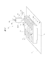
以下、本発明の通信モジュールの実施形態の一例について説明する。本実施形態に係る通信モジュールは、他の複数の通信モジュールと共に不図示の電子機器に実装される。具体的には、本実施形態に係る通信モジュール及び他の通信モジュールは、電子機器が備える基板(以下“マザーボード”と呼ぶ。)上に設けられているスロットに抜き差しされる。通信モジュールがスロットに差し入れられると、通信モジュールが備えるコネクタとスロットに内包されているコネクタとが接続される。すなわち、通信モジュールがマザーボードに実装される。また、マザーボード上には、通信モジュールを冷却するための放熱部材が設けられており、この放熱部材の一部によって上記スロットが形成されている。スロットに差し入れられた通信モジュールは、放熱部材の吸熱面として機能するスロットの内側面に接触し、放熱部材と熱的に接続される。
(First embodiment)
Hereinafter, an example of an embodiment of a communication module of the present invention will be described. The communication module according to the present embodiment is mounted on an electronic device (not shown) together with a plurality of other communication modules. Specifically, the communication module according to the present embodiment and other communication modules are inserted into and removed from slots provided on a board (hereinafter referred to as “mother board”) included in the electronic device. When the communication module is inserted into the slot, the connector provided in the communication module and the connector contained in the slot are connected. That is, the communication module is mounted on the motherboard. Further, a heat radiating member for cooling the communication module is provided on the motherboard, and the slot is formed by a part of the heat radiating member. The communication module inserted into the slot contacts the inner surface of the slot that functions as the heat absorbing surface of the heat radiating member, and is thermally connected to the heat radiating member.
そこで、初めに電子機器の構成について説明し、次いで、本実施形態に係る通信モジュールの構成について説明する。尚、本実施形態に係る通信モジュールは、同一の形状及び構造を有する他の複数の通信モジュールと共に電子機器のマザーボード上に高密度実装されるが、本明細書に添付の図面では他の通信モジュールの図示は省略されている。 Therefore, the configuration of the electronic device will be described first, and then the configuration of the communication module according to the present embodiment will be described. Note that the communication module according to the present embodiment is mounted on the motherboard of the electronic device together with a plurality of other communication modules having the same shape and structure, but the other communication modules are shown in the drawings attached to this specification. Is not shown.
図1に示されるように、電子機器が備えるマザーボード2の略中央には、通信用半導体チップ3が実装されている。また、通信用半導体チップ3の周囲には複数のコネクタ(レセプタクルコネクタ4)が配置されている。それぞれのレセプタクルコネクタ4は、マザーボード2に形成されている不図示の配線を介して通信用半導体チップ3と電気的に接続されている。
As shown in FIG. 1, a
マザーボード2に実装されている通信用半導体チップ3の上にはヒートシンク5が重ねて搭載されており、通信用半導体チップ3の上面とヒートシンク5の底面とは、不図示の熱伝導シートを介して接触している。すなわち、通信用半導体チップ3とヒートシンク5とは熱的に接続されている。ヒートシンク5はマザーボード2に固定されており、ヒートシンク5の内部にはジグザグに蛇行する冷媒流路6が形成されている。冷媒流路6の一端は、ヒートシンク5の上面に形成されている接続プラグ7に連通し、冷媒流路6の他端は、ヒートシンク5の上面に形成されている他の接続プラグ8に連通している。一方の接続プラグ7には不図示の冷媒供給パイプが接続され、他方の接続プラグ8には不図示の冷媒回収パイプが接続される。電子機器に内蔵されている不図示のポンプによって、冷媒供給パイプ及び接続プラグ7を介してヒートシンク5に冷媒(例えば、水)が供給される。ヒートシンク5に供給された冷媒は、冷媒流路6を通過し、接続プラグ8及び冷媒回収パイプを介してポンプに回収される。すなわち、ヒートシンク5には冷媒が循環される。
A
ヒートシンク5の対向する二辺は、レセプタクルコネクタ4を避けるように櫛歯状に形成されている。具体的には、ヒートシンク5の一辺には、該一辺に沿って複数のスリット9が形成され、ヒートシンク5の他の一辺には、該一辺に沿って複数のスリット9が形成されている。ヒートシンク5がマザーボード2上の所定位置に搭載されると、それぞれのレセプタクルコネクタ4が所定のスリット9の内側に収まる。すなわち、通信用半導体チップ3はヒートシンク5に覆われるが、レセプタクルコネクタ4はヒートシンク5に覆われない。具体的には、それぞれのレセプタクルコネクタ4の三方がスリット9の内側面によって囲まれる。換言すれば、ヒートシンク5の一部によって、マザーボード2上に、レセプタクルコネクタ4を内包する複数のスロットが形成される。そこで、以下の説明では、ヒートシンク5に形成されている各スリット9を“スロット9”と呼ぶ場合がある。
Two opposing sides of the
次に、本実施形態に係る通信モジュールについて詳細に説明する。図2に示されるように、通信モジュール1Aは、ヒートシンク5の一部によって形成されている各スロット9の開口部10から該スロット9に抜き差しされる。
Next, the communication module according to the present embodiment will be described in detail. As shown in FIG. 2, the
通信モジュール1Aは、板金によって形成された略直方体形状の筐体20を有する。通信モジュール1Aの筐体20は、互いに対向する上面板21及び底面板22、正面板23及び背面板24、第1側面板25及び第2側面板26、を有する。以下の説明では、第1側面板25及び第2側面板26を“側面板27”と総称する場合がある。また、上面板21と底面板22の対向方向を“高さ方向”と定義し、第1側面板25と第2側面板26の対向方向を“幅方向”と定義し、正面板23と背面板24の対向方向を“厚み方向”と定義する。かかる定義に従えば、通信モジュール1Aは、高さ方向及び幅方向の寸法に比べて厚み方向の寸法が小さい薄型のモジュールである。
The communication module 1A includes a substantially
通信モジュール1Aの筐体20には、通信ケーブルとしての光ファイバ30が接続される光接続部40が設けられている。また、筐体20には、モジュールコネクタとしてのプラグコネクタ50が設けられている。プラグコネクタ50は、筐体20の底面板22から突出しており、図1に示されるレセプタクルコネクタ4に挿抜される。
The
図3に示されるように、筐体20は、プレス成形された第1部材20aと第2部材20bとから構成されている。第1部材20aと第2部材20bとは、互いに付き合わされ、内部に収容空間を有する筐体20を形成している。より具体的には、第1部材20aによって図2に示される正面板23が形成され、第2部材20bによって図2に示される背面板を形成され、第1部材20a及び第2部材20bの双方によって図2に示される上面板21,底面板22及び側面板27が形成されている。
As shown in FIG. 3, the
図3,図4に示されるように、筐体20の内部にはモジュール基板60が収容されている。モジュール基板60は、対向する第1部材20aと第2部材20bとの間に配置されており、筐体20の内面とは非接触である。換言すれば、モジュール基板60は、筐体20の内部においてフローティング状態とされている。以下の説明では、筐体20の内面のうち、正面板23の内面を“第1内面23a”と呼び、筐体20の背面板24の内面を“第2内面24a”と呼ぶ。すなわち、筐体20は対向する第1内面23aと第2内面24aとを備えており、モジュール基板60は第1内面23aと第2内面24aとの間に配置されている。尚、図4では、図3に示される光接続部40の図示は省略されている。
As shown in FIGS. 3 and 4, a
図4に示されるように、筐体20の第1内面23aと対向するモジュール基板60の表面60aには半導体素子が搭載されている。具体的には、モジュール基板60の表面60aには、発光素子(不図示)及び発光素子を駆動する駆動素子(駆動用IC)61が搭載されている。また、図示はされていないが、モジュール基板60の表面60aには、受光素子及び受光素子の出力を増幅する増幅素子(増幅用IC)も搭載されている。
As shown in FIG. 4, a semiconductor element is mounted on the
一方、筐体20の第2内面24aと対向するモジュール基板60の裏面60bには、発光素子及び受光素子と図2に示される光ファイバ30とを光結合させる樹脂レンズ62が搭載されている。
On the other hand, a
さらに、プラグコネクタ50がモジュール基板60の下辺60cに装着されている。換言すれば、プラグコネクタ50が装着されている一辺がモジュール基板60の下辺60cであり、この下辺60cと対向する他の一辺がモジュール基板の上辺60dである。もっとも、モジュール基板60の一辺に、モジュールコネクタとしてのエッジコネクタ(カードエッジ)が形成される実施形態もある。かかる実施形態においては、エッジコネクタ(カードエッジ)が形成されている一辺がモジュール基板60の下辺であり、この下辺と対向する他の一辺がモジュール基板60の上辺である。
Further, the
モジュール基板60の表面60aに搭載されている半導体素子は、モジュール基板60の表面60aに被せられたカバー部材63によって覆われている。カバー部材63は熱伝導性に優れた金属(本実施形態ではアルミニウム)によって形成されている。カバー部材63と筐体20の第1内面23aとの間には熱伝導部材64が配置されており、この熱伝導部材64を介してカバー部材63と筐体20とが熱的に接続されている。具体的には、熱伝導部材64の一面がカバー部材63に密着し、熱伝導部材64の他の一面が筐体20の第1内面23aに密着している。
The semiconductor element mounted on the
本実施形態における熱伝導部材64は、柔軟性及び放熱性を備えたゴムである。熱伝導部材64は、圧力を受けると、カバー部材63及び筐体20に対する密着を維持したまま変形して厚みを変化させる。
The
再び図3を参照する。筐体20の第2内面24aには、モジュール基板60を支持する一対の支持部材70が設けられている。それぞれの支持部材70は角柱状であって、第2内面24aから第1内面23a(図4)に向かって突出している。図3,図4に示されるように、モジュール基板60は、支持部材70の上に載置され、固定部材としての螺子71によって支持部材70に固定されている。具体的には、図3に示されるように、モジュール基板60に形成されている貫通孔65に挿入された螺子71が支持部材70の端面に形成されている螺子穴72に結合されている。モジュール基板60に形成されている2つの貫通孔65は、モジュール基板60の幅方向両側に位置している。また、これら貫通孔65は、モジュール基板60の高さ方向に関しては略中央に位置している。換言すれば、貫通孔65は、モジュール基板60の上辺60dと下辺60cの略中間に位置している(図4)。このように、モジュール基板60は、上辺60dと下辺60cの略中間において2点支持されている。
Refer to FIG. 3 again. A pair of
さらに、図3,図4に示されるように、モジュール基板60の表面60aと螺子71の頭部との間にはスプリングワッシャ73が介在している。また、モジュール基板60の裏面60bと支持部材70の端面との間にもスプリングワッシャ74が介在している。
Further, as shown in FIGS. 3 and 4, a
従って、モジュール基板60に図4中の矢印a方向又は矢印b方向の力が作用した際、モジュール基板60は、スプリングワッシャ73,74を圧縮しながら同方向に揺動する。すなわち、モジュール基板60は、支持部材70を支点とし搖動可能に支持されている。具体的には、モジュール基板60は、上辺60dが筐体20の第1内面23aに近接する方向(矢印b方向)と、上辺60dが筐体20の第2内面24aに近接する方向(矢印a方向)と、に揺動可能である。かかるモジュール基板60の搖動に伴って熱伝導部材64に圧力が加わり、熱伝導部材64の厚みが変化することは明らかである。具体的には、モジュール基板60が矢印b方向に揺動した場合には、熱伝導部材64の上部の厚みは相対的に薄くなり、下部の厚みは相対的に厚くなる。一方、モジュール基板60が矢印a方向に揺動した場合には、熱伝導部材64の上部の厚みは相対的に厚くなり、下部の厚みは相対的に薄くなる。
Therefore, when a force in the direction of arrow a or b in FIG. 4 is applied to the
図3,図4に示されるように、筐体20には押圧部材が一体成形されている。具体的には、背面板24の一部が外側へ向けて折り曲げられ、押圧部材としての弾性片80を形成している。尚、弾性片80は、通信モジュール1Aの筐体20に形成せず、ヒートシンク5のスロット10(図1)に形成してもよい。
As shown in FIGS. 3 and 4, a pressing member is integrally formed with the
図4に示される正面板23の外面23bと弾性片80との間の間隔(D1)は、図2に示されるスロット9の対向する内側面9a,9bの間の間隔(D2)よりも広い。よって、図5に示されるように、通信モジュール1Aがスロット9に差し入れられ、プラグコネクタ50がレセプタクルコネクタ4に接続(嵌合)されると、弾性片80はスロット9の一方の内側面9bに当接して弾性変形する。この結果、弾性片80の復元力によって筐体20がスロット9の他方の内側面9aに向けて押圧され、筐体20の正面板23(図4)の外面23bがスロット9の内側面9aに押し付けられる。すなわち、筐体20の一面(外面23b)とスロット9の内側面9aとが接触し、筐体20とスロット9(ヒートシンク5)とが熱交換可能に接続される。換言すれば、スロット9の内側面9aはヒートシンク5の吸熱面であり、筐体20の外面23bは放熱面であり、これら吸熱面と放熱面とが熱的に接続される。
The distance (D1) between the
ここで、レセプタクルコネクタ4及びヒートシンク5はマザーボード2に強固に固定されている。また、レセプタクルコネクタ4は雌型の多ピンコネクタであって、プラグコネクタ50は雄型の多ピンコネクタである。よって、レセプタクルコネクタ4に嵌合されたプラグコネクタ50は、レセプタクルコネクタ4の各ピンに挟まれて固定される。かかる状況の下で筐体20がスロット9の内側面(吸熱面)9aに向けて押圧されると、様々な公差に起因してプラグコネクタ50やモジュール基板60(図4)などに力が作用する。特に、内側面(吸熱面)9aからレセプタクルコネクタ4の中心までの距離と内側面(吸熱面)9aからプラグコネクタ50の中心までの距離とが異なると、プラグコネクタ50やモジュール基板60などに図4に示される矢印a方向又は矢印b方向の力が作用する。
Here, the
この点、本実施形態に係る通信モジュール1Aでは、モジュール基板60が図4に示される矢印a方向及び矢印b方向に揺動可能に支持されている。よって、プラグコネクタ50やモジュール基板60に矢印a方向又は矢印b方向の力が作用しても、これらに応力が発生することがないか、応力が大幅に低減されるので、プラグコネクタ50やモジュール基板60が歪むことがない。これにより、モジュール基板60上の電子部品が外れたり、破損したりする虞がない。すなわち、モジュール基板60が搖動することによって公差が吸収される。また、吸熱面と放熱面との接触、すなわち熱的接続も確実に担保される。さらに、モジュール基板60を支持部材70に固定している螺子71は、該モジュール基板60を貫通している。すなわち、モジュール基板60はプラグコネクタ50の挿抜方向(図4の紙面上下方向)において固定されている。よって、モジュール基板60がフローティング状態(搖動可能)であっても、プラグコネクタ50の挿抜に支障はない。尚、モジュール基板60は、図4の紙面に対して垂直な方向においても固定されている。
In this regard, in the communication module 1A according to the present embodiment, the
図3,図4に示される螺子71の支持部材70に対する結合を弱めれば、スプリングワッシャ73,74がなくとも、モジュール基板60を上記のように搖動可能に支持することができる。また、支持部材70の強度に異方性を持たせることによってモジュール基板60を上記のように搖動可能に支持することもできる。すなわち、支持部材70の強度をモジュール基板60の搖動方向においては相対的に低く、それ以外の方向においては相対的に高くすれば、モジュール基板60を上記のように搖動可能に支持することができる。
If the connection of the
(第2の実施形態)
以下、本発明の通信モジュールの実施形態の他の一例について説明する。もっとも、本実施形態に係る通信モジュールは、第1の実施形態に係る通信モジュールと同一の基本構成を備えている。そこで、既に説明した構成と同一又は実質的に同一の構成については適宜説明を省略する。
(Second Embodiment)
Hereinafter, another example of the embodiment of the communication module of the present invention will be described. However, the communication module according to the present embodiment has the same basic configuration as the communication module according to the first embodiment. Therefore, the description of the same or substantially the same configuration as already described will be omitted as appropriate.
図6に示されるように、本実施形態に係る通信モジュール1Bにおいては、支持部材70が筐体20の第1内面23aから突出している。支持部材70は、熱伝導部材64を貫通しており、熱伝導部材64から突出している支持部材70の先端がカバー部材63に当接している。具体的には、支持部材70の先端は球状に形成されており、この先端がカバー部材63の天井に形成されている球状の凹部90に嵌合されている。
As shown in FIG. 6, in the
一方、モジュール基板60の裏面60bと筐体20の第2内面24aとの間には、弾性部材としてのコイルばね91が配置されており、このコイルばね91の上にモジュール基板60が載置されている。すなわち、モジュール基板60は、コイルばね91によって弾性的に支持されている。換言すれば、コイルばね91は、モジュール基板60を支持する第2の支持部材である。
On the other hand, a
本実施形態におけるモジュール基板60も、支持部材70を支点として図中の矢印a方向及び矢印b方向に揺動可能である。よって、プラグコネクタ50やモジュール基板60に矢印a方向又は矢印b方向の力が作用しても、これらに応力が発生することがないか、応力が大幅に低減される。すなわち、モジュール基板60が搖動することによって公差が吸収される。また、吸熱面と放熱面との接触、すなわち熱的接続も確実に担保される。さらに、カバー部材63に当接している支持部材70の先端は、カバー部材63に形成されている凹部90に嵌合されている。すなわち、モジュール基板60はプラグコネクタ50の挿抜方向(図6の紙面上下方向)において固定されている。尚、モジュール基板60は、図6の紙面に対して垂直な方向においても固定されている。尚、図6では、光接続部40の図示は省略されている。
The
(第3の実施形態)
以下、本発明の通信モジュールの実施形態の他の一例について説明する。もっとも、本実施形態に係る通信モジュールは、第1の実施形態に係る通信モジュールと同一の基本構成を備えている。そこで、既に説明した構成と同一又は実質的に同一の構成については適宜説明を省略する。
(Third embodiment)
Hereinafter, another example of the embodiment of the communication module of the present invention will be described. However, the communication module according to the present embodiment has the same basic configuration as the communication module according to the first embodiment. Therefore, the description of the same or substantially the same configuration as already described will be omitted as appropriate.
図7に示されるように、本実施形態に係る通信モジュール1Cにおいては、一対の円柱状の支持部材70がカバー部材63の側面から互いに逆向きに突出している。これら支持部材70は、筐体20の互いに対向する内面に回動可能に固定されている。具体的には、筐体20の第1側面板25の内面(第3内面25a)及び第2側面板26の内面(第4内面26a)には、それぞれ係合穴92が形成されている。一方の支持部材70の先端は第3内面25aに形成されている係合穴92に挿入され、他方の支持部材70の先端は第4内面26aに形成されている係合穴92に挿入されている。
As shown in FIG. 7, in the
本実施形態おけるモジュール基板60も、支持部材70を支点(回動軸)として図4や図6に示されている矢印a方向及び矢印b方向に揺動可能(回動可能)である。
The
本発明は上記実施形態に限定されるものではなく、その要旨を逸脱しない範囲で種々変更可能である。例えば、支持部材70の形状,数,配置など適宜変更することができる。例えば、図3に示される支持部材70の形状は円柱形に変更可能である。また、図3に示される支持部材70は、筐体20の幅方向に伸びる板状の支持部材に変更可能である。図6に示される支持部材70の形状は円錐形に変更可能である。要するに、モジュール基板60が支持部材70を支点として搖動可能に支持されている限り、モジュール基板60と支持部材70との接触態様は、点接触,線接触、面接触の何れの態様であってもよい。
The present invention is not limited to the above-described embodiment, and various modifications can be made without departing from the scope of the invention. For example, the shape, number, and arrangement of the
また、支持部材70によるモジュール基板60の支持点も上記実施形態に限定されない。例えば、図3,図4に示されているモジュール基板60は、上辺60dと下辺60cの略中間において支持部材70によって支持されている。すなわち、モジュール基板60の支持点は、上辺60dと下辺60cの略中間にある。しかし、貫通孔65及び支持部材70の位置を変更して、支持点を上下に移動させることもできる。もっとも、支持点(貫通孔65及び支持部材70の位置)を上下に移動させると、モジュール基板60の搖動量が大きくなり、熱伝導部材64とカバー部材63とが非接触となる虞がある。例えば、支持点を図4に示されている位置よりも上辺60dに近接した位置に移動させると、モジュール基板60の下辺60c側の揺動量が大きくなる。このため、モジュール基板60が矢印b方向に揺動したときに、カバー部材63の下部が熱伝導部材64から離間する虞がある。一方、支持点を図4に示されている位置よりも下辺60cに近接した位置に移動させると、モジュール基板60の上辺60d側の搖動量が大きくなる。このため、モジュール基板60が矢印a方向に揺動したときに、カバー部材63の上部が熱伝導部材64から離間する虞がある。従って、熱伝導部材64とカバー部材63との接触をバランス良く維持する観点からは、モジュール基板60を上辺60dと下辺60cの略中間において支持することが好ましい。
Further, the support point of the
図4や図6に示される熱伝導部材64は、流動性を有する粘性充填剤に置換可能である。例えば、熱伝導部材64は、2枚の樹脂フィルムの間に金属箔が挟まれたラミネートフィルムによって形成された袋の中に粘性充填剤としての金属ペーストが封入された放熱バッグに置換可能である。かかる放熱バッグは、圧力を受けると、袋内で金属ペーストが流動し、厚みが変化する。また、金属ペーストの緩やかな流動によって、モジュール基板60のスムーズな揺動が実現される。
The
マザーボード2に設けられるコネクタがプラグコネクタであり、モジュール基板60に装着または形成されるモジュールコネクタがレセプタクルコネクタである実施形態もある。
In some embodiments, the connector provided on the
図1,図2に示されているヒートシンク5の全ての辺にスロット9が形成され、それぞれのスロット9に通信モジュールが挿入される実施形態もある。また、ヒートシンク5の3辺にスロット9が形成される実施形態もある。さらに、電子機器が備えるスロットの一部にのみ通信モジュールが挿入され、残りのスロットが空きスロットになる場合もある。
In some embodiments,
本発明は光通信モジュールのみではく、電気通信モジュールにも適用可能であり、電気通信モジュールに適用された場合にも上記と同様の作用効果が得られる。本発明が適用された電気通信モジュールでは、図2に示される光接続部40に替えて電気接続部が設けられ、この電気接続部に電気通信ケーブルが接続される。また、筐体の内部には、電気通信機能その他の機能を実現するために必要な各種要素が収容される。
The present invention can be applied not only to an optical communication module but also to a telecommunication module, and the same effects as described above can be obtained when applied to a telecommunication module. In the telecommunication module to which the present invention is applied, an electric connecting portion is provided instead of the optical connecting
1A,1B,1C 通信モジュール
2 マザーボード
4 レセプタクルコネクタ
5 ヒートシンク
9 スリット(スロット)
9a,9b 内側面
20 筐体
21 上面板
22 底面板
23 正面板
23a 第1内面
23b 外面
24 背面板
24a 第2内面
25 第1側面板
25a 第3内面
26 第2側面板
26a 第4内面
27 側面板
50 プラグコネクタ
60 モジュール基板
60a 表面
60b 裏面
60c 下辺
60d 上辺
63 カバー部材
64 熱伝導部材
70 支持部材
71 螺子
73,74 スプリングワッシャ
80 弾性片
91 コイルばね
92 係合穴
1A, 1B,
9a, 9b
Claims (8)
モジュール基板が収容された筐体と、
前記筐体から突出し、前記電子機器が備える前記基板上のコネクタに挿抜されるモジュールコネクタと、
前記筐体の内部において前記モジュール基板を支持する支持部材と、を有し、
前記モジュール基板は、前記筐体と非接触であり、前記支持部材を支点として搖動可能に支持されている、
通信モジュール。 A communication module mounted on a board included in an electronic device,
A housing containing the module substrate; and
A module connector that protrudes from the housing and is inserted into and removed from the connector on the board provided in the electronic device,
A support member that supports the module substrate inside the housing;
The module substrate is non-contact with the housing and is supported so as to be slidable with the support member as a fulcrum.
Communication module.
前記筐体の一面であって、前記基板上に設けられている放熱部材の吸熱面と熱的に接続される放熱面と、
前記筐体を前記吸熱面に向けて押圧する押圧部材と、を有する、
通信モジュール。 The communication module according to claim 1,
One surface of the housing, and a heat radiating surface thermally connected to a heat absorbing surface of a heat radiating member provided on the substrate,
A pressing member that presses the housing toward the endothermic surface.
Communication module.
前記筐体は、対向する第1内面及び第2内面を備え、
前記モジュール基板は、前記第1内面と対向する表面と、前記第2内面と対向する裏面と、前記モジュールコネクタが装着された下辺と、該下辺と対向する上辺と、を備え、
前記モジュール基板は、前記上辺が前記第1内面に近接する方向と前記第2内面に近接する方向とに揺動可能である、
通信モジュール。 The communication module according to claim 1 or 2,
The housing includes a first inner surface and a second inner surface facing each other,
The module substrate includes a surface facing the first inner surface, a back surface facing the second inner surface, a lower side on which the module connector is mounted, and an upper side facing the lower side,
The module substrate is swingable in a direction in which the upper side is close to the first inner surface and a direction in which the upper side is close to the second inner surface.
Communication module.
前記筐体は、対向する第1内面及び第2内面を備え、
前記モジュール基板は、前記第1内面と対向する表面と、前記第2内面と対向する裏面と、前記モジュールコネクタが形成された下辺と、該下辺と対向する上辺と、を備え、
前記モジュール基板は、前記上辺が前記第1内面に近接する方向と前記第2内面に近接する方向とに揺動可能である、
通信モジュール。 The communication module according to claim 1 or 2,
The housing includes a first inner surface and a second inner surface facing each other,
The module substrate includes a surface facing the first inner surface, a back surface facing the second inner surface, a lower side on which the module connector is formed, and an upper side facing the lower side,
The module substrate is swingable in a direction in which the upper side is close to the first inner surface and a direction in which the upper side is close to the second inner surface.
Communication module.
前記モジュール基板の前記表面に搭載された半導体素子と、
前記半導体素子を覆うカバー部材と、
前記カバー部材と前記筐体の前記第1内面との間に配置された熱伝導部材と、を有し、
前記カバー部材と前記筐体とが前記熱伝導部材を介して熱的に接続され、
前記熱伝導部材は、前記モジュール基板の搖動に伴って厚みが変化する柔軟性を備えている、
通信モジュール。 The communication module according to claim 3 or 4,
A semiconductor element mounted on the surface of the module substrate;
A cover member covering the semiconductor element;
A heat conducting member disposed between the cover member and the first inner surface of the housing;
The cover member and the housing are thermally connected via the heat conducting member,
The heat conducting member has a flexibility that changes in thickness as the module substrate swings.
Communication module.
前記支持部材が前記筐体の前記第2内面から突出し、
前記モジュール基板の前記裏面が前記支持部材の上に載置されている、
通信モジュール。 The communication module according to any one of claims 3 to 5,
The support member protrudes from the second inner surface of the housing;
The back surface of the module substrate is placed on the support member;
Communication module.
前記支持部材が前記筐体の前記第1内面から突出して前記カバー部材に当接し、
前記モジュール基板が該モジュール基板の前記裏面と前記筐体の前記第2内面との間に配置された弾性部材の上に載置されている、
通信モジュール。 The communication module according to claim 5,
The support member protrudes from the first inner surface of the housing and contacts the cover member;
The module substrate is placed on an elastic member disposed between the back surface of the module substrate and the second inner surface of the housing.
Communication module.
一対の前記支持部材が前記カバー部材の側面から互いに逆向きに突出し、
前記一対の支持部材の一方が前記筐体の第3内面に回動可能に固定され、前記一対の支持部材の他方が前記第3内面と対向する第4内面に回動可能に固定されている、
通信モジュール。 The communication module according to claim 5,
A pair of the support members project in opposite directions from the side surfaces of the cover member;
One of the pair of support members is pivotally fixed to the third inner surface of the housing, and the other of the pair of support members is pivotally fixed to a fourth inner surface facing the third inner surface. ,
Communication module.
Priority Applications (2)
| Application Number | Priority Date | Filing Date | Title |
|---|---|---|---|
| JP2014235240A JP2016100426A (en) | 2014-11-20 | 2014-11-20 | Communication module |
| US14/924,767 US20160150673A1 (en) | 2014-11-20 | 2015-10-28 | Communication Module |
Applications Claiming Priority (1)
| Application Number | Priority Date | Filing Date | Title |
|---|---|---|---|
| JP2014235240A JP2016100426A (en) | 2014-11-20 | 2014-11-20 | Communication module |
Publications (1)
| Publication Number | Publication Date |
|---|---|
| JP2016100426A true JP2016100426A (en) | 2016-05-30 |
Family
ID=56011672
Family Applications (1)
| Application Number | Title | Priority Date | Filing Date |
|---|---|---|---|
| JP2014235240A Pending JP2016100426A (en) | 2014-11-20 | 2014-11-20 | Communication module |
Country Status (2)
| Country | Link |
|---|---|
| US (1) | US20160150673A1 (en) |
| JP (1) | JP2016100426A (en) |
Cited By (3)
| Publication number | Priority date | Publication date | Assignee | Title |
|---|---|---|---|---|
| JP2020107310A (en) * | 2018-12-26 | 2020-07-09 | 廣達電腦股▲ふん▼有限公司Quanta Computer Inc. | Common carrier for different types of cards |
| CN111970897A (en) * | 2020-08-06 | 2020-11-20 | 中国电子科技集团公司第三十八研究所 | Heat exchange radiator is reinforceed to semi-enclosed island type rib pole side hole vortex |
| WO2021006214A1 (en) * | 2019-07-05 | 2021-01-14 | 日東電工株式会社 | Opto-electro transmission module |
Families Citing this family (4)
| Publication number | Priority date | Publication date | Assignee | Title |
|---|---|---|---|---|
| JP2016091734A (en) * | 2014-10-31 | 2016-05-23 | 日立金属株式会社 | Communication module |
| TWI556707B (en) * | 2015-12-17 | 2016-11-01 | 技嘉科技股份有限公司 | Electronic assembly |
| JP6649854B2 (en) * | 2016-07-21 | 2020-02-19 | レノボ・シンガポール・プライベート・リミテッド | Electronics |
| CN109152313A (en) * | 2018-10-26 | 2019-01-04 | 浙江佳乐科仪股份有限公司 | A kind of radiator of high efficiency and heat radiation |
Family Cites Families (27)
| Publication number | Priority date | Publication date | Assignee | Title |
|---|---|---|---|---|
| US4341428A (en) * | 1980-03-24 | 1982-07-27 | Pintek, Inc. | Interconnection system for shielded electrical cable |
| JPH0330378U (en) * | 1989-07-21 | 1991-03-26 | ||
| US5380216A (en) * | 1992-05-11 | 1995-01-10 | The Whitaker Corporation | Cable backpanel interconnection |
| US5561727A (en) * | 1994-02-15 | 1996-10-01 | Sumitomo Electric Industries, Ltd. | Card-shaped optical data link device |
| USRE40150E1 (en) * | 1994-04-25 | 2008-03-11 | Matsushita Electric Industrial Co., Ltd. | Fiber optic module |
| JP3326959B2 (en) * | 1994-04-25 | 2002-09-24 | 松下電器産業株式会社 | Optical fiber module |
| US5435744A (en) * | 1994-05-19 | 1995-07-25 | The Whitaker Corporation | Sliding boot assembly for electrical connector |
| US5879173A (en) * | 1995-01-13 | 1999-03-09 | Methode Electronics, Inc. | Removable transceiver module and receptacle |
| US5734558A (en) * | 1995-01-13 | 1998-03-31 | Poplawski; Daniel S. | Removable optoelectronic module |
| US5836774A (en) * | 1996-11-12 | 1998-11-17 | Hon Hai Precision Ind. Co., Ltd. | Adapter and mechanism thereof |
| US6244889B1 (en) * | 1998-01-20 | 2001-06-12 | Intel Corporation | Method and apparatus for an electromechanically controlled electronic interface plug |
| WO2000008503A1 (en) * | 1998-08-04 | 2000-02-17 | Sumitomo Electric Industries, Ltd. | Optical module connector adaptor, optical module product, and optical module mounting substrate product |
| JP3605586B2 (en) * | 2001-09-25 | 2004-12-22 | 日本圧着端子製造株式会社 | Flexible board connector |
| US6916123B2 (en) * | 2002-09-10 | 2005-07-12 | Jds Uniphase Corporation | Unlatching mechanism for an optical transceiver |
| US6808400B2 (en) * | 2002-10-18 | 2004-10-26 | Aiptek International Inc. | USB connector structure with protection means |
| JP2005106584A (en) * | 2003-09-30 | 2005-04-21 | Mitsubishi Electric Corp | Acceleration sensor unit |
| KR100617710B1 (en) * | 2004-05-21 | 2006-08-28 | 삼성전자주식회사 | Latching apparatus for pluggable optical transceiver module |
| US7448899B2 (en) * | 2005-04-22 | 2008-11-11 | Delta Electronics, Inc. | Connecting module for communication |
| US7766672B1 (en) * | 2009-06-24 | 2010-08-03 | Cameo Communication, Inc. | Electronic connector with a circuit board sandwiched between two spacers and enclosed in a frame |
| TWM372554U (en) * | 2009-09-03 | 2010-01-11 | Tai Sol Electronics Co Ltd | Poka-yoke all-in-one card connector for single-card insertion only |
| JP5112484B2 (en) * | 2010-08-19 | 2013-01-09 | 日本航空電子工業株式会社 | connector |
| US8348684B2 (en) * | 2010-12-17 | 2013-01-08 | Research In Motion Limited | Portable electronic device having a concealed jack socket |
| JP5737244B2 (en) * | 2012-09-03 | 2015-06-17 | 日立金属株式会社 | Communication module cooling structure and communication device |
| TWI607675B (en) * | 2013-12-13 | 2017-12-01 | 台達電子企業管理(上海)有限公司 | Dc/dc power module and dc/dc power system assembly |
| JP6281424B2 (en) * | 2014-06-24 | 2018-02-21 | 日立金属株式会社 | Communication module |
| JP2016024976A (en) * | 2014-07-22 | 2016-02-08 | 日立金属株式会社 | Communication module |
| JP2016091734A (en) * | 2014-10-31 | 2016-05-23 | 日立金属株式会社 | Communication module |
-
2014
- 2014-11-20 JP JP2014235240A patent/JP2016100426A/en active Pending
-
2015
- 2015-10-28 US US14/924,767 patent/US20160150673A1/en not_active Abandoned
Cited By (5)
| Publication number | Priority date | Publication date | Assignee | Title |
|---|---|---|---|---|
| JP2020107310A (en) * | 2018-12-26 | 2020-07-09 | 廣達電腦股▲ふん▼有限公司Quanta Computer Inc. | Common carrier for different types of cards |
| WO2021006214A1 (en) * | 2019-07-05 | 2021-01-14 | 日東電工株式会社 | Opto-electro transmission module |
| JP2021012941A (en) * | 2019-07-05 | 2021-02-04 | 日東電工株式会社 | Optical-electric composite transmission module |
| JP7359579B2 (en) | 2019-07-05 | 2023-10-11 | 日東電工株式会社 | Optical and electrical composite transmission module |
| CN111970897A (en) * | 2020-08-06 | 2020-11-20 | 中国电子科技集团公司第三十八研究所 | Heat exchange radiator is reinforceed to semi-enclosed island type rib pole side hole vortex |
Also Published As
| Publication number | Publication date |
|---|---|
| US20160150673A1 (en) | 2016-05-26 |
Similar Documents
| Publication | Publication Date | Title |
|---|---|---|
| JP2016100426A (en) | Communication module | |
| US10517166B2 (en) | Optical transceiver including heat dissipation structure | |
| US9124025B2 (en) | Connector | |
| JP5224416B2 (en) | Optical module mounting unit and optical module | |
| US9807899B2 (en) | Storage device | |
| US9568695B2 (en) | Package structure of optical connector | |
| TW201607160A (en) | Thermally efficient connector system | |
| US8267159B2 (en) | Thermal module | |
| JP2011170566A (en) | Semiconductor storage device and electronic device | |
| JP2016167571A (en) | Electronic device | |
| US11127649B2 (en) | Electronic apparatus | |
| US9739960B2 (en) | Optical module heat dissipation structure and electronic product | |
| JP2014049691A (en) | Cooling structure of communication module and communication device | |
| US9230882B2 (en) | Signal transmission device | |
| JP2016170712A (en) | Server system and storage device | |
| CN109219307B (en) | Heat radiation structure and electronic device with same | |
| US20190223325A1 (en) | Optical module | |
| JP5323518B2 (en) | Parallel optical transmission equipment | |
| JPS62261199A (en) | Heat radiation structure of printed wiring board on ehich electronic parts are mounted | |
| TWM459676U (en) | Server device | |
| US9874708B2 (en) | Optical module blind mating heat relay system | |
| JP2014178383A (en) | Communication module and signal transmission device provided with the same | |
| CN113923958A (en) | Display module and display device | |
| JP7196470B2 (en) | Heat dissipation structure of electronic equipment | |
| US20160231516A1 (en) | Communication Module and Signal Transmission Device Including the Same |