JP2016018628A - Signal transmission cable - Google Patents
Signal transmission cable Download PDFInfo
- Publication number
- JP2016018628A JP2016018628A JP2014139392A JP2014139392A JP2016018628A JP 2016018628 A JP2016018628 A JP 2016018628A JP 2014139392 A JP2014139392 A JP 2014139392A JP 2014139392 A JP2014139392 A JP 2014139392A JP 2016018628 A JP2016018628 A JP 2016018628A
- Authority
- JP
- Japan
- Prior art keywords
- signal
- wiring board
- processing circuit
- transmission
- terminals
- Prior art date
- Legal status (The legal status is an assumption and is not a legal conclusion. Google has not performed a legal analysis and makes no representation as to the accuracy of the status listed.)
- Pending
Links
Images


Classifications
-
- H—ELECTRICITY
- H04—ELECTRIC COMMUNICATION TECHNIQUE
- H04B—TRANSMISSION
- H04B3/00—Line transmission systems
- H04B3/02—Details
- H04B3/04—Control of transmission; Equalising
-
- H—ELECTRICITY
- H04—ELECTRIC COMMUNICATION TECHNIQUE
- H04B—TRANSMISSION
- H04B3/00—Line transmission systems
- H04B3/50—Systems for transmission between fixed stations via two-conductor transmission lines
Landscapes
- Engineering & Computer Science (AREA)
- Computer Networks & Wireless Communication (AREA)
- Signal Processing (AREA)
- Dc Digital Transmission (AREA)
- Details Of Connecting Devices For Male And Female Coupling (AREA)
- Coupling Device And Connection With Printed Circuit (AREA)
- Cable Transmission Systems, Equalization Of Radio And Reduction Of Echo (AREA)
- Insulated Conductors (AREA)
- Communication Cables (AREA)
Abstract
Description
本発明は、信号伝送用ケーブルに関するものである。 The present invention relates to a signal transmission cable.
特許文献1には、コネクタ付ケーブルに関する技術が記載されている。この文献に記載されたコネクタ付ケーブルは、ケーブルの両端にコネクタが取り付けられたものである。このコネクタ付ケーブルでは、受信側コネクタ又は送信側コネクタが、受信信号又は送信信号の波形整形を行うための波形整形素子を内蔵する。
近年、通信機器間のデータ伝送のために、クロックデータリカバリ(CDR)回路などの信号処理回路をコネクタ内に内蔵するコネクタ付ケーブルが使用されている。このようなケーブルは、例えば、データセンターにおけるサーバ、ストレージ、スイッチといった各装置の相互間の接続に好適に用いられる。従来、このようなケーブルとして、いわゆるツイストペアケーブルやツイナックスケーブルが用いられている。その場合、一方の装置から出力された差動信号を構成する一対の信号それぞれを、ツイストペア線もしくはツイナックス線を構成する一対の電線それぞれを通して他方の装置へ伝送する。 In recent years, a cable with a connector in which a signal processing circuit such as a clock data recovery (CDR) circuit is built in a connector is used for data transmission between communication devices. Such a cable is preferably used for connection between devices such as servers, storages, and switches in a data center. Conventionally, so-called twisted pair cables and twinax cables are used as such cables. In that case, a pair of signals constituting a differential signal output from one device is transmitted to the other device through a pair of electric wires constituting a twisted pair wire or a twinax wire.
しかし、ツイストペアケーブルやツイナックスケーブルは、2本の電線からなるので一般的に曲げにくく、配線の作業性が低いという問題を有する。特に最近では、通信データ量の急激な増加によってデータセンター等における装置間の配線本数が増大しているので、装置間の配線が容易であることは重要となっている。 However, twisted pair cables and twinax cables are generally difficult to bend because they are composed of two electric wires, and have a problem that the workability of wiring is low. Particularly recently, the number of wirings between devices in a data center or the like has increased due to a rapid increase in the amount of communication data, so that it is important that wiring between devices is easy.
このような問題を解決するために、ツイストペアケーブルに代えて柔軟性に優れた同軸ケーブルを使用することが考えられる。しかしながら、差動信号を構成する一対の信号を2本の同軸ケーブルを通して伝送すると、2本の同軸ケーブルの長さや電気的特性が異なる場合に、差動信号を構成する一対の信号の位相が互いにずれてスキューが生じ、伝送損失が増大してしまうおそれがある。 In order to solve such a problem, it is conceivable to use a coaxial cable excellent in flexibility instead of the twisted pair cable. However, when a pair of signals constituting a differential signal are transmitted through two coaxial cables, the phase of the pair of signals constituting the differential signal is mutually different when the length and electrical characteristics of the two coaxial cables are different. There is a possibility that skew occurs and transmission loss increases.
本発明は、装置間の配線の作業性を高めつつ、伝送損失を抑えることができる信号伝送用ケーブルを提供することを目的とする。 An object of the present invention is to provide a signal transmission cable capable of suppressing transmission loss while improving workability of wiring between apparatuses.
上述した課題を解決するために、本発明による信号伝送用ケーブルは、外部装置の内部回路と電気的に接続される信号処理回路を有し、外部装置に対して挿抜可能に構成されたコネクタと、信号処理回路と電気的に接続された金属線とを備え、信号処理回路は、送信処理部及び受信処理部の一方又は双方を有し、送信処理部は、外部装置からの送信信号を受け、金属線へ受信信号を出力し、受信処理部は、金属線からの受信信号を受け、外部装置へ出力信号を出力し、送信信号及び出力信号は差動信号であり、受信信号はシングルエンド信号である。 In order to solve the above-described problems, a signal transmission cable according to the present invention includes a signal processing circuit that is electrically connected to an internal circuit of an external device, and a connector configured to be inserted into and removed from the external device. The signal processing circuit includes one or both of a transmission processing unit and a reception processing unit, and the transmission processing unit receives a transmission signal from an external device. The reception processing unit outputs the reception signal to the metal wire, the reception processing unit receives the reception signal from the metal wire, outputs the output signal to the external device, the transmission signal and the output signal are differential signals, and the reception signal is single-ended. Signal.
本発明による信号伝送用ケーブルによれば、装置間の配線の作業性を高めつつ、伝送損失を抑えることができる。 According to the signal transmission cable of the present invention, it is possible to suppress transmission loss while improving workability of wiring between devices.
[本願発明の実施形態の説明]
最初に、本願発明の実施形態の内容を列記して説明する。(1)本願発明による信号伝送用ケーブルは、外部装置の内部回路と電気的に接続される信号処理回路を有し、外部装置に対して挿抜可能に構成されたコネクタと、信号処理回路と電気的に接続された金属線とを備え、信号処理回路は、送信処理部及び受信処理部の一方又は双方を有し、送信処理部は、外部装置からの送信信号を受け、金属線へ受信信号を出力し、受信処理部は、金属線からの受信信号を受け、外部装置へ出力信号を出力し、送信信号及び出力信号は差動信号であり、受信信号はシングルエンド信号である。
[Description of Embodiment of Present Invention]
First, the contents of the embodiment of the present invention will be listed and described. (1) A signal transmission cable according to the present invention has a signal processing circuit electrically connected to an internal circuit of an external device, a connector configured to be inserted into and removed from the external device, a signal processing circuit, and an electric circuit. The signal processing circuit has one or both of a transmission processing unit and a reception processing unit, and the transmission processing unit receives a transmission signal from an external device and receives the reception signal to the metal line. The reception processing unit receives a reception signal from the metal wire and outputs an output signal to an external device. The transmission signal and the output signal are differential signals, and the reception signal is a single-ended signal.
通常、外部装置間のデータ伝送には差動信号が用いられる。この信号伝送用ケーブルは、送信処理部において、外部装置からの送信信号を差動信号として受ける。そして、この送信信号をシングルエンド信号として出力する。また、この信号伝送用ケーブルは、受信処理部において、受信信号をシングルエンド信号として受け、この受信信号を差動信号として出力する。これにより、送信信号および受信信号を1本の金属線によって伝送することができるので、例えば同軸ケーブルといった単線ケーブルを用いることによって、スキューの発生による伝送損失の増大を抑えることができる。また、ツイストペアケーブルやツイナックスケーブルではなく同軸ケーブル等の単線ケーブルを使用できるので、信号伝送用ケーブルを柔軟で細径にできる。従って、装置間の配線の作業性を高めることができる。 Normally, differential signals are used for data transmission between external devices. This signal transmission cable receives a transmission signal from an external device as a differential signal in a transmission processing unit. Then, this transmission signal is output as a single-ended signal. In the signal transmission cable, the reception processing unit receives the reception signal as a single-ended signal and outputs the reception signal as a differential signal. Thereby, since the transmission signal and the reception signal can be transmitted by one metal line, an increase in transmission loss due to the occurrence of skew can be suppressed by using a single line cable such as a coaxial cable. Further, since a single wire cable such as a coaxial cable can be used instead of a twisted pair cable or a twinax cable, the signal transmission cable can be made flexible and thin. Therefore, the workability of wiring between devices can be improved.
(2)上記の信号伝送用ケーブルにおいて、金属線は、信号処理回路の端子に交流的に短絡されてもよい。このように、金属線と信号処理回路との間に他の信号処理回路部品(バラン、コモンモードチョーク等)が介在しないことによって、伝送損失の更なる抑制及びコスト低減を図ることができる。また、他の回路部品を不要とすることによってコネクタの小型化に寄与できる。 (2) In the above signal transmission cable, the metal wire may be short-circuited to the terminal of the signal processing circuit in an AC manner. Thus, since no other signal processing circuit components (balun, common mode choke, etc.) are interposed between the metal line and the signal processing circuit, transmission loss can be further suppressed and cost can be reduced. Further, it is possible to contribute to miniaturization of the connector by eliminating the need for other circuit components.
(3)上記の信号伝送用ケーブルにおいて、送信処理部は、送信信号を差動信号として出力する一対の出力端子を有し、一対の出力端子の一方は終端されており、一対の出力端子の他方が金属線に交流的に接続されてもよい。これにより、差動信号として受けた送信信号を、シングルエンド信号として出力する機能を好適に実現することができる。 (3) In the signal transmission cable described above, the transmission processing unit has a pair of output terminals that output the transmission signal as a differential signal, one of the pair of output terminals is terminated, and the pair of output terminals The other may be connected to the metal wire in an alternating manner. Thereby, it is possible to suitably realize a function of outputting a transmission signal received as a differential signal as a single-ended signal.
(4)上記の信号伝送用ケーブルにおいて、受信処理部は、受信信号を入力するための一対の入力端子を有し、受信信号は一対の入力端子の一方に入力され、一対の入力端子の他方は終端されてもよい。これにより、シングルエンド信号として受けた受信信号を、差動信号として出力する機能を好適に実現することができる。 (4) In the signal transmission cable, the reception processing unit includes a pair of input terminals for inputting the reception signal, and the reception signal is input to one of the pair of input terminals, and the other of the pair of input terminals. May be terminated. Thereby, the function of outputting the received signal received as a single end signal as a differential signal can be suitably realized.
(5)上記の信号伝送用ケーブルにおいて、コネクタは配線基板を更に有し、配線基板は、信号処理回路を実装する実装領域と、信号処理回路と電気的に接続され、外部装置との電気的なインターフェースを構成する接続部と、信号処理回路と電気的に接続されるとともに金属線が導電接着されたパッドとを有してもよい。 (5) In the signal transmission cable, the connector further includes a wiring board, and the wiring board is electrically connected to the mounting area for mounting the signal processing circuit, the signal processing circuit, and electrically connected to the external device. And a pad that is electrically connected to the signal processing circuit and to which a metal wire is conductively bonded.
(6)上記の信号伝送用ケーブルにおいて、信号処理回路の一部分が配線基板の一方の面上の実装領域に実装されており、信号処理回路の他の部分が配線基板の他方の面上の実装領域に実装されてもよい。これにより、配線基板上において信号処理回路を余裕をもって実装することができ、配線基板上の配線の間隔を広くして配線間のクロストークを低減することができる。 (6) In the above signal transmission cable, a part of the signal processing circuit is mounted on the mounting area on one side of the wiring board, and the other part of the signal processing circuit is mounted on the other side of the wiring board. It may be implemented in the area. Thereby, the signal processing circuit can be mounted on the wiring board with a margin, and the interval between the wirings on the wiring board can be widened to reduce crosstalk between the wirings.
(7)上記の信号伝送用ケーブルにおいて、接続部を構成する一部の端子が一方の面上に設けられており、接続部を構成する他の端子が他方の面上に設けられており、一部の端子は信号処理回路の一部分と電気的に接続されており、他の端子は信号処理回路の他の部分と電気的に接続されてもよい。 (7) In the signal transmission cable, a part of the terminals constituting the connection part is provided on one surface, and the other terminals constituting the connection part are provided on the other surface, Some terminals may be electrically connected to a part of the signal processing circuit, and other terminals may be electrically connected to other parts of the signal processing circuit.
(8)上記の信号伝送用ケーブルにおいて、信号処理回路が配線基板の一方の面及び他方の面のうち一方の面上の実装領域に実装されてもよい。これにより、信号処理回路を配線基板上に実装する工程を短縮することができる。 (8) In the signal transmission cable, the signal processing circuit may be mounted on a mounting region on one of the one surface and the other surface of the wiring board. Thereby, the process of mounting the signal processing circuit on the wiring board can be shortened.
(9)上記の信号伝送用ケーブルにおいて、接続部を構成する一部の端子が一方の面上に設けられており、接続部を構成する他の端子が他方の面上に設けられており、一部の端子及び他の端子は一方の面上の信号処理回路と電気的に接続されてもよい。 (9) In the signal transmission cable, a part of the terminals constituting the connection part is provided on one surface, and the other terminals constituting the connection part are provided on the other surface, Some terminals and other terminals may be electrically connected to a signal processing circuit on one surface.
(10)上記の信号伝送用ケーブルにおいて、パッドが配線基板の一方の面上にのみ設けられてもよい。これにより、金属線を半田等によってパッドに接続する作業を容易にできる。 (10) In the signal transmission cable, the pad may be provided only on one surface of the wiring board. Thereby, the operation | work which connects a metal wire to a pad by solder etc. can be made easy.
(11)上記の信号伝送用ケーブルにおいて、パッドが配線基板の一方の面上及び他方の面上の双方に設けられてもよい。これにより、パッド間隔及び金属線の間隔を広くすることができ、信号間のクロストークを低減することができる。 (11) In the signal transmission cable described above, pads may be provided on both the one surface and the other surface of the wiring board. Thereby, the pad interval and the metal line interval can be widened, and crosstalk between signals can be reduced.
(12)上記の信号伝送用ケーブルにおいて、配線基板の一方の面上及び他方の面上のそれぞれにパッドが複数設けられており、各面上において、複数のパッドが配線基板の隅に偏って配置されてもよい。これにより、配線基板上の実装面積を広くすることができる。 (12) In the above signal transmission cable, a plurality of pads are provided on each of the one surface and the other surface of the wiring board, and the plurality of pads are biased to the corners of the wiring board on each surface. It may be arranged. Thereby, the mounting area on a wiring board can be enlarged.
(13)上記の信号伝送用ケーブルにおいて、コネクタは、信号処理回路及び配線基板を収容するハウジングを更に有し、ハウジングと他方の面との間隔が、ハウジングと一方の面との間隔よりも狭くてもよい。このように、配線基板の片側の面とハウジングとの間隔が狭い場合であっても、上記の信号伝送用ケーブルによれば、例えば金属線が一方の面にのみ配置されることによって、他方の面上に電子部品を好適に配置することができる。 (13) In the signal transmission cable, the connector further includes a housing that accommodates the signal processing circuit and the wiring board, and a distance between the housing and the other surface is narrower than a distance between the housing and the one surface. May be. Thus, even when the distance between one surface of the wiring board and the housing is narrow, according to the signal transmission cable, for example, the metal wire is disposed only on one surface, so that the other An electronic component can be suitably arranged on the surface.
[本願発明の実施形態の詳細]
本発明の実施形態に係る信号伝送用ケーブルの具体例を、以下に図面を参照しつつ説明する。なお、本発明はこれらの例示に限定されるものではなく、特許請求の範囲によって示され、特許請求の範囲と均等の意味及び範囲内でのすべての変更が含まれることが意図される。以下の説明では、図面の説明において同一の要素には同一の符号を付し、重複する説明を省略する。
[Details of the embodiment of the present invention]
A specific example of a signal transmission cable according to an embodiment of the present invention will be described below with reference to the drawings. In addition, this invention is not limited to these illustrations, is shown by the claim, and intends that all the changes within the meaning and range equivalent to the claim are included. In the following description, the same reference numerals are given to the same elements in the description of the drawings, and redundant descriptions are omitted.
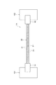
図1は、本発明の一実施形態に係る信号伝送用ケーブル1Aの構成を示す図である。図1に示されるように、本実施形態の信号伝送用ケーブル1Aは、2つのコネクタ10と、ケーブル束20とを備える。一方のコネクタ10はケーブル束20の一端に取り付けられており、他方のコネクタ10はケーブル束20の他端に取り付けられている。ケーブル束20は、複数本の同軸ケーブル21が束ねられて成る。一方のコネクタ10は、外部装置101に対して挿抜可能に構成されており、外部装置101に挿入されることによって外部装置101と電気的に接続される。他方のコネクタ10は、別の外部装置102に対して挿抜可能に構成されており、外部装置102に挿入されることによって外部装置102と電気的に接続される。
FIG. 1 is a diagram showing a configuration of a
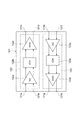
図2は、信号伝送用ケーブル1Aの構成の一部を概略的に示すブロック図である。図2に示されるように、2つのコネクタ10は信号処理回路12をそれぞれ有する。信号処理回路12は、例えばクロックデータリカバリ(CDR)回路やリピータ回路等の信号整形回路を含み、該信号整形回路は集積回路素子(IC)121によって構成されている。一方のコネクタ10の信号処理回路12は、該コネクタ10が外部装置101に挿入されることにより、外部装置101の内部回路と電気的に接続される。また、他方のコネクタ10の信号処理回路12は、該コネクタ10が外部装置102に挿入されることにより、外部装置102の内部回路と電気的に接続される。
FIG. 2 is a block diagram schematically showing a part of the configuration of the
信号処理回路12は、送信処理部122及び受信処理部123を有する。送信処理部122は、集積回路素子121の一部分を含んで構成されている。集積回路素子121の当該部分は、外部装置101又は102からの送信信号S1を一対の入力端子121a,121bに受ける。ここで、送信信号S1は、相補的な一対の信号(正相信号Sa1及び逆相信号Sb1)からなる差動信号である。また、送信処理部122は終端回路124を有する。終端回路124は、例えば、集積回路素子121の当該部分の一対の出力端子121c,121dのうち一方(出力端子121d)とグランド配線GNDとの間に接続された50オームの終端抵抗及びコンデンサを含んで構成される。なお、出力端子121dは電源線等に接続されていても良い。
The
送信処理部122において、集積回路素子121は、送信信号S1に基づき整形された差動信号を、一対の出力端子121c,121dから出力する。そのうち、一方の出力端子121dは終端されている。具体的には、出力端子121dには終端回路124が接続されている。これにより、正相信号及び逆相信号のうち一方は消滅する。なお、出力端子121dは電源線等に接続されていても良い。また、他方の出力端子121cは、ケーブル束20に含まれる一本の同軸ケーブル21の心線(金属線)21aと電気的に接続されている。一例では、他方の出力端子121cは、心線21aとコンデンサ等を介して交流的に短絡されている。正相信号及び逆相信号のうち他方は、受信信号S2として同軸ケーブル21の心線21aに出力する。受信信号S2は、正相信号Sa1及び逆相信号Sb1のうちのいずれかのみからなるシングルエンド信号である。受信信号S2は、同軸ケーブル21を介して他方のコネクタ10へ伝送される。
In the
受信処理部123は、集積回路素子121の別の一部分を含んで構成されている。集積回路素子121の当該部分は、一対の入力端子121e,121fを有する。一対の入力端子121e,121fのうち一方(入力端子121e)は、同軸ケーブル21の心線21aと電気的に接続されている。一例では、入力端子121eは、心線21aとコンデンサ等を介して交流的に短絡されている。また、一対の入力端子121e,121fのうち他方(入力端子121f)は、終端されている。具体的には、受信処理部123は終端回路125を有する。終端回路125は、例えば、一対の入力端子121e,121fのうち他方(入力端子121f)とグランド配線GNDとの間に接続された終端抵抗及びコンデンサを含んで構成される。従って、入力端子121fはグランド電位(基準電位)とされる。なお、入力端子121fは電源線等に接続されていても良い。集積回路素子121は、他方のコネクタ10からのシングルエンド信号である受信信号S2を、同軸ケーブル21を介して入力端子121eに受ける。
The
受信処理部123において、集積回路素子121は、受信信号S2に基づき整形された出力信号S3を、一対の出力端子121g,121hから出力する。出力信号S3は、正相信号Sa2及び逆相信号Sb2からなる差動信号である。この出力信号S3は、外部装置101又は102へ出力される。
In the
なお、図2には各コネクタ10の信号処理回路12が送信処理部122及び受信処理部123の双方を有する例について示されているが、信号処理回路12は、送信処理部122及び受信処理部123のうち何れか双方のみを有してもよい。例えば、一方のコネクタ10の信号処理回路12が送信処理部122のみを有し、他方のコネクタ10の信号処理回路12が受信処理部123のみを有してもよい。
2 illustrates an example in which the
図3は、集積回路素子121の内部構成の一例(リタイマIC)を示す図である。図3に示されるように、集積回路素子121のうち送信処理部122を構成する部分は、イコライザ(EQ)122aと、クロックデータリカバリ回路(CDR)122bと、ドライバ(Driver)122cとを有する。EQ122aの差動入力は一対の入力端子121a,121bと接続されており、EQ122aの差動出力はCDR122bの差動入力に接続されている。CDR122bの差動出力はドライバ122cの差動入力に接続されており、ドライバ122cの差動出力は一対の出力端子121c,121dと接続されている。
FIG. 3 is a diagram illustrating an example (retimer IC) of the internal configuration of the
また、集積回路素子121のうち受信処理部123を構成する部分は、EQ123aと、CDR123bと、ドライバ123cとを有する。EQ123aの差動入力は一対の入力端子121e,121fと接続されており、EQ123aの差動出力はCDR123bの差動入力に接続されている。CDR123bの差動出力はドライバ123cの差動入力に接続されており、ドライバ123cの差動出力は一対の出力端子121g,121hと接続されている。
In addition, a part of the
なお、図3では集積回路素子121がリタイマICである場合を例示したが、集積回路素子121はリピータIC等の他の信号整形ICであってもよい。集積回路素子121がリピータICである場合、図3に示されるCDR122b及び123bは不要となる。
3 illustrates the case where the
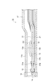
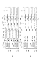
図4及び図5は、コネクタ10の具体的な構成例を示す図である。図4はコネクタ10の側断面図であり、図5(a)はコネクタ10が有する配線基板13を一方の板面側から見た上面図であり、図5(b)は配線基板13を他方の板面側から見た裏面図である。
4 and 5 are diagrams illustrating a specific configuration example of the
図4及び図5に示されるように、本実施形態のコネクタ10は、配線基板13を更に有する。配線基板13は、長手方向及び短手方向を有する長方形状を呈しており、誘電体基板と、該誘電体基板の一方の面13a上及び他方の面13b上に形成された導電性の配線パターンとを有する。配線基板13は、信号処理回路12を実装する領域(実装領域)と、信号処理回路12に電気的に接続された接続部14及びパッド群15とを有する。
As shown in FIGS. 4 and 5, the
本実施形態では、実装領域は配線基板13の一方の面13a及び他方の面13bの双方に設けられている。そして、信号処理回路12の一部分12Aが配線基板13の一方の面13a上の実装領域に実装されており、信号処理回路12の他の部分12Bが配線基板13の他方の面13b上の実装領域に実装されている。図5(a)に示されるように、信号処理回路12の一部分12Aは、一つの集積回路素子121を有しており、2つの送信処理部122と、2つの受信処理部123とを含む。また、図5(b)に示されるように、信号処理回路12の他の部分12Bは、一つの集積回路素子121を有しており、2つの送信処理部122と、2つの受信処理部123とを含む。なお、図5では、終端回路124及び125の図示が省略されている。
In the present embodiment, the mounting area is provided on both the one
接続部14は、外部装置101,102(図1及び図2を参照)との電気的なインターフェースを構成する部分である。接続部14は、一方の面13a上及び他方の面13b上に設けられた複数の端子14a〜14dを有する。具体的には、一方の面13a上及び他方の面13b上のそれぞれに、一対の端子14a及び14bからなる2つの組と、一対の端子14c及び14dからなる2つの組とが設けられている。一対の端子14a及び14bは、例えば送信用の信号端子であり、それぞれ対応する送信処理部122の入力端子121a及び121bと接続されている。一対の端子14c及び14dは、例えば受信用の信号端子であり、それぞれ対応する受信処理部123の出力端子121g及び121hと接続されている。なお、図5では、信号端子(端子14a〜14d)以外の端子、例えば電源端子やグランド端子等は省略されている。
The
パッド群15は、配線基板13の一方の面13a上に設けられており、4つのパッド15aと、4つのパッド15bとを有する。パッド15a及び15bには、同軸ケーブル21の心線21aの一端が導電接着されている。パッド15a及び15bの幅は、心線21aの直径の1.2倍ないし2.0倍である。また、パッド15a同士及びパッド15b同士の間隔は、パッド15a及び15bの幅よりも大きい。
The
パッド15aは、例えば送信用のパッドである。2つのパッド15aは、信号処理回路12の一部分12Aにおいてそれぞれ対応する送信処理部122の出力端子121cと交流的に接続(短絡)されている。他の2つのパッド15aは、他の部分12Bにおいてそれぞれ対応する送信処理部122の出力端子121cと、スルーホール16aを介して交流的に接続(短絡)されている。また、パッド15bは、例えば受信用のパッドである。2つのパッド15bは、信号処理回路12の一部分12Aにおいてそれぞれ対応する受信処理部123の入力端子121eと交流的に接続(短絡)されている。他の2つのパッド15bは、他の部分12Bにおいてそれぞれ対応する受信処理部123の入力端子121eと、スルーホール16bを介して交流的に接続(短絡)されている。
The
図4に示されるように、コネクタ10はハウジング17を更に有する。ハウジング17は、信号処理回路12及び配線基板13を収容する筐体である。ハウジング17は、配線基板13の長手方向に沿って延びる中空の直方体状を呈しており、配線基板13の一方の面13aと対向する天板17aと、配線基板13の他方の面13bと対向する底板17bとを有する。また、ハウジング17の前端部は開口しており、接続部14と共に電気コネクタ18を構成する。ハウジング17の後端部からは、複数の同軸ケーブル21が導入されている。一実施例では、ハウジング17の底板17bと他方の面13bとの間隔D1が、ハウジング17の天板17aと一方の面13aとの間隔D2よりも狭い。
As shown in FIG. 4, the
以上の構成を備える本実施形態の信号伝送用ケーブル1Aによって得られる効果について説明する。通常、外部装置101,102間のデータ伝送には差動信号が用いられる。この信号伝送用ケーブル1Aは、送信処理部122において、外部装置101又は102からの差動信号である送信信号S1を受ける。そして、該送信信号をシングルエンド信号である受信信号S2として出力する。また、この信号伝送用ケーブル1Aは、受信処理部123において、受信信号S2をシングルエンド信号として受ける。そして、該受信信号を差動信号である出力信号S3として出力する。これにより、受信信号S2を1本の金属線によって伝送することができるので、例えば同軸ケーブル21といった単線ケーブルを用いることによって、スキューの発生による伝送損失の増大を抑えることができる。また、ツイストペアケーブルやツイナックスケーブルではなく同軸ケーブル21等の単線ケーブルを使用できるので、信号伝送用ケーブル1Aを柔軟で細径にできる。従って、外部装置101と外部装置102との間の配線の作業性を高めることができる。もしくは、差動信号を送受信する構成と比較して、信号伝送用ケーブル1Aを同じ太さに構成した場合であっても、それぞれの同軸ケーブル21をより太くすることができるので、受信信号S2が伝送中に減衰しにくくなる。従って、同じ太さのケーブルでも、より長距離の伝送が可能になる。
The effect obtained by the
また、本実施形態のように、同軸ケーブル21の心線21aは、信号処理回路12の各端子121c、121eに短絡されてもよい。このように、心線21aと信号処理回路12との間に他の回路部品(バラン、コモンモードチョーク等)が介在しないことによって、伝送損失の更なる抑制及びコスト低減を図ることができる。また、他の回路部品を不要とすることによってコネクタ10の小型化に寄与できる。
Further, as in the present embodiment, the
また、本実施形態のように、送信処理部122は、一対の出力端子121c及び121dの一方とグランド配線GNDとの間に接続された終端抵抗を含む終端回路124を有し、一対の出力端子121c及び121dの他方が心線21aに接続されてもよい。これにより、差動信号として受けた送信信号S1を、シングルエンド信号である受信信号S2として出力する機能を好適に実現することができる。
Further, as in the present embodiment, the
また、本実施形態のように、受信処理部123が受信信号S2を入力するための一対の入力端子121e及び121fを有しており、シングルエンド信号である受信信号S2は一対の入力端子121e及び121fの一方に入力され、一対の入力端子121e及び121fの他方はグランド電位とされてもよい。これにより、シングルエンド信号として受けた受信信号S2を、差動信号である出力信号S3として出力する機能を好適に実現することができる。
Further, as in the present embodiment, the
また、本実施形態のように、コネクタ10は配線基板13を有し、配線基板13は、実装領域と、接続部14と、パッド15a及び15bとを有してもよい。これにより、外部装置101,102と、信号処理回路12と、同軸ケーブル21とを互いに電気的に接続する構成を容易に実現することができる。
Further, as in the present embodiment, the
また、本実施形態のように、信号処理回路12の一部分12Aが配線基板13の一方の面13a上の実装領域に実装されており、信号処理回路12の他の部分12Bが配線基板13の他方の面13b上の実装領域に実装されてもよい。これにより、配線基板13上において信号処理回路12を余裕をもって実装することができ、配線基板13上の配線の間隔を広くして配線間のクロストークを低減することができる。
Further, as in this embodiment, a
また、本実施形態のように、接続部14を構成する一部の端子が一方の面13a上に設けられており、接続部14を構成する他の端子が他方の面13b上に設けられてもよい。更に、その一部の端子は信号処理回路12の一部分12Aと電気的に接続されており、他の端子は信号処理回路12の他の部分12Bと電気的に接続されてもよい。これにより、一方の面13a上及び他方の面13a上のそれぞれにおいて、接続部14の端子と信号処理回路12とを好適に接続することができる。
Further, as in the present embodiment, some terminals constituting the
また、本実施形態のように、パッド15a及び15bが、配線基板13の一方の面13a上にのみ設けられてもよい。これにより、配線基板13において同軸ケーブル21が片面実装となり、多数の心線21aを半田等によってパッド15a及び15bに接続する作業を容易にできる。
Further, the
また、本実施形態のように、ハウジング17と他方の面13bとの間隔D1が、ハウジング17と一方の面13aとの間隔D2よりも狭くてもよい。例えば、従来のQSFPモジュールでは配線基板の両面に同軸ケーブルが配置される。従って、配線基板の何れかの面とハウジングとの間隔が狭い場合には、当該面上に電子部品を実装することが困難となる場合がある。これに対し、本実施形態のコネクタ10によれば、配線基板13の片側の面とハウジング17との間隔が狭い場合であっても、同軸ケーブル21が一方の面13a上にのみ配置されることによって、他方の面13b上に電子部品を好適に配置することができる。
Further, as in the present embodiment, the interval D1 between the
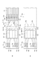
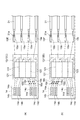
(第1の変形例)
図6は、第1変形例として、配線基板13Aの構成例を示す図である。図6(a)は配線基板13Aを一方の板面側から見た上面図であり、図6(b)は配線基板13Aを他方の板面側から見た裏面図である。なお、以下に説明する点を除き、配線基板13Aの形態は上記実施形態の配線基板13(図5を参照)と同様である。
(First modification)
FIG. 6 is a diagram illustrating a configuration example of a
本変形例では、実装領域は配線基板13Aの一方の面13a及び他方の面13bのうち一方(例えば一方の面13a)にのみ設けられている。そして、信号処理回路12の全部が一方の面13a上の実装領域に実装されている。図6(a)に示されるように、信号処理回路12は、一つの集積回路素子121を有しており、4つの送信処理部122と、4つの受信処理部123とを含む。なお、図6では、終端回路124及び125の図示が省略されている。
In the present modification, the mounting area is provided only on one (for example, one
一方の面13a上に設けられた接続部14の端子14a及び14bは、それぞれ対応する送信処理部122の入力端子121a及び121bと接続されている。同様に、一方の面13a上に設けられた接続部14の端子14c及び14dは、それぞれ対応する受信処理部123の出力端子121g及び121hと接続されている。また、他方の面13b上に設けられた接続部14の端子14a及び14bは、スルーホール16cを介して、それぞれ対応する送信処理部122の入力端子121a及び121bと接続されている。同様に、他方の面13b上に設けられた接続部14の端子14c及び14dは、スルーホール16dを介して、それぞれ対応する受信処理部123の出力端子121g及び121hと接続されている。
The
送信用の4つのパッド15aは、一方の面13a上においてそれぞれ対応する送信処理部122の出力端子121cと交流的に接続(短絡)されている。また、受信用の4つのパッド15bは、一方の面13a上においてそれぞれ対応する受信処理部123の入力端子121eと交流的に接続(短絡)されている。
The four
本変形例によれば、上記実施形態と同様に、外部装置101,102間の配線の作業性を高めつつ、スキューの発生による伝送損失の増大を抑えることができる。更に、本変形例によれば、信号処理回路12の全部が配線基板13Aの一方の面13a上の実装領域にのみ実装されているので、信号処理回路12を配線基板13A上に実装する工程を短縮することができるとともに、配線基板13Aの他方の面13b上において他の回路の実装領域を広くすることができる。
According to this modification, as in the above embodiment, it is possible to improve the workability of the wiring between the
また、本実施形態のように、接続部14を構成する一部の端子が一方の面13a上に設けられており、接続部14を構成する他の端子が他方の面13b上に設けられてもよい。更に、それら一部の端子及び他の端子の双方が、一方の面13a上の信号処理回路12と電気的に接続されてもよい。このような形態であっても、上述した実施形態の効果を好適に奏することができる。
Further, as in the present embodiment, some terminals constituting the
(第2の変形例)
図7は、第2変形例として、配線基板13Bの構成例を示す図である。図7(a)は配線基板13Bを一方の板面側から見た上面図であり、図7(b)は配線基板13Bを他方の板面側から見た裏面図である。なお、以下に説明する点を除き、配線基板13Bの形態は第1変形例の配線基板13A(図6を参照)と同様である。
(Second modification)
FIG. 7 is a diagram illustrating a configuration example of a
本変形例の配線基板13Bは、上記第1変形例のパッド群15に代えて、パッド群15A及び15Bを有する。パッド群15Aは、配線基板13の一方の面13a上に設けられており、2つのパッド15aと、2つのパッド15bとを有する。また、パッド群15Bは、配線基板13の他方の面13b上に設けられており、送信用の2つのパッド15aと、受信用の2つのパッド15bとを有する。
The
パッド群15Aの2つのパッド15aは、それぞれ対応する送信処理部122の出力端子121cに対し、一方の面13a上の配線を介して交流的に接続(短絡)されている。パッド群15Bの2つのパッド15aは、それぞれ対応する送信処理部122の出力端子121cに対し、他方の面13b上の配線及びスルーホール16aを介して交流的に接続(短絡)されている。また、パッド群15Aの2つのパッド15bは、それぞれ対応する受信処理部123の入力端子121eに対し、一方の面13a上の配線を介して交流的に接続(短絡)されている。パッド群15Bの2つのパッド15bは、それぞれ対応する受信処理部123の入力端子121eに対し、他方の面13b上の配線及びスルーホール16bを介して交流的に接続(短絡)されている。
The two
本変形例によれば、上記実施形態と同様に、外部装置101,102間の配線の作業性を高めつつ、スキューの発生による伝送損失の増大を抑えることができる。また、本変形例のように、パッド15a及び15bが、一方の面13a上及び他方の面13b上の双方に設けられてもよい。これにより、パッド間隔及び心線21aの間隔を広くすることができ、信号間のクロストークを低減することができる。
According to this modification, as in the above embodiment, it is possible to improve the workability of the wiring between the
ここで、信号間のクロストークには、送信信号同士、若しくは受信信号同士のクロストーク(Far End CrossTalk;FEXT)と、送信信号と受信信号との間のクロストーク(Near End CrossTalk;NEXT)とがある。本変形例によれば、パッド間隔及び心線21aの間隔を広くして、NEXT及びFEXTの双方を効果的に抑えることができる。
Here, crosstalk between signals includes crosstalk between transmission signals or reception signals (Far End CrossTalk; FEXT), and crosstalk between transmission signals and reception signals (Near End CrossTalk; NEXT). There is. According to this modification, both the NEXT and the FEXT can be effectively suppressed by widening the pad interval and the interval between the
(第3の変形例)
図8は、第3変形例として、配線基板13Cの構成例を示す図である。図8(a)は配線基板13Cを一方の板面側から見た上面図であり、図8(b)は配線基板13Cを他方の板面側から見た裏面図である。なお、以下に説明する点を除き、配線基板13Cの形態は上記実施形態の配線基板13(図5を参照)と同様である。
(Third Modification)
FIG. 8 is a diagram illustrating a configuration example of a
本変形例の配線基板13Cは、上記実施形態のパッド群15に代えて、パッド群15A及び15Bを有する。パッド群15Aは、配線基板13の一方の面13a上に設けられており、2つのパッド15aと、2つのパッド15bとを有する。また、パッド群15Bは、配線基板13の他方の面13b上に設けられており、送信用の2つのパッド15aと、受信用の2つのパッド15bとを有する。
The
パッド群15Aの2つのパッド15aは、信号処理回路12の一部分12Aにおいてそれぞれ対応する送信処理部122の出力端子121cと交流的に接続(短絡)されている。パッド群15Bの2つのパッド15aは、他の部分12Bにおいてそれぞれ対応する送信処理部122の出力端子121cと交流的に接続(短絡)されている。また、パッド群15Aの2つのパッド15bは、信号処理回路12の一部分12Aにおいてそれぞれ対応する受信処理部123の入力端子121eと交流的に接続(短絡)されている。パッド群15Bの2つのパッド15bは、他の部分12Bにおいてそれぞれ対応する受信処理部123の入力端子121eと交流的に接続(短絡)されている。
The two
本変形例によれば、上記実施形態と同様に、外部装置101,102間の配線の作業性を高めつつ、スキューの発生による伝送損失の増大を抑えることができる。また、本変形例のように、パッド15a及び15bが、一方の面13a上及び他方の面13b上の双方に設けられてもよい。これにより、パッド間隔及び心線21aの間隔を広くすることができ、信号間のクロストークを低減することができる。
According to this modification, as in the above embodiment, it is possible to improve the workability of the wiring between the
(第4の変形例)
図9は、上記実施形態の第4変形例として、配線基板13Dの構成例を示す図である。図9(a)は配線基板13Dを一方の板面側から見た上面図であり、図9(b)は配線基板13Dを他方の板面側から見た裏面図である。なお、以下に説明する点を除き、配線基板13Dの形態は第3変形例の配線基板13C(図8を参照)と同様である。
(Fourth modification)
FIG. 9 is a diagram illustrating a configuration example of a
本変形例の配線基板13Dは、第3変形例のパッド群15A及び15Bに代えて、パッド群15C及び15Dを有する。パッド群15Cは、配線基板13の一方の面13a上に設けられており、2つのパッド15aと、2つのパッド15bとを有する。そして、これら複数のパッドは、配線基板13Dの隅に偏って配置されている。具体的には、パッド群15Cの複数のパッドは、配線基板13Dの長手方向に沿った一対の辺のうち一方に寄って配置されており、パッド間隔は第3変形例よりも小さい。
The
また、パッド群15Dは、配線基板13の他方の面13b上に設けられており、2つのパッド15aと、2つのパッド15bとを有する。そして、これら複数のパッドは、配線基板13Dの隅に偏って配置されている。具体的には、パッド群15Dの複数のパッドのうち一部は、配線基板13Dの長手方向に沿った一対の辺の一方に寄って配置されており、残りは、該一対の辺の他方に寄って配置されている。
The
本変形例のように、各面13a及び13b上において、複数のパッドは配線基板13Dの隅に偏って配置されてもよい。これにより、配線基板13D上の実装面積を広くすることができる。
Like this modification, a plurality of pads may be arranged so as to be biased to the corners of the
(第5の変形例)
図10は、上記実施形態の第5変形例として、配線基板13Eの構成例を示す図である。図10(a)は配線基板13Eを一方の板面側から見た上面図であり、図10(b)は配線基板13Eを他方の板面側から見た裏面図である。なお、以下に説明する点を除き、配線基板13Eの形態は第3変形例の配線基板13C(図8を参照)と同様である。
(Fifth modification)
FIG. 10 is a diagram illustrating a configuration example of a wiring board 13E as a fifth modification of the embodiment. FIG. 10A is a top view of the wiring board 13E viewed from one plate surface side, and FIG. 10B is a back view of the wiring substrate 13E viewed from the other plate surface side. Except as described below, the form of the wiring board 13E is the same as that of the
本変形例の配線基板13Eは、第3変形例の信号処理回路12の部分12A及び12Bに代えて、部分12C及び12Dを有する。信号処理回路12の一部分12Cは、配線基板13Eの一方の面13a上の実装領域に実装されており、信号処理回路12の他の部分12Dは、配線基板13Eの他方の面13b上の実装領域に実装されている。各部分12A及び12Bは、それぞれ一つの集積回路素子121を有する。但し、本変形例では、部分12Cが4つの送信処理部122を含んでおり、部分12Dが4つの受信処理部123を含んでいる。
A wiring board 13E of this modification has
一方の面13a上に設けられた接続部14の端子14a及び14bは、一方の面13a上に設けられた配線を介して、それぞれ対応する送信処理部122の入力端子121a及び121bと接続されている。他方の面13a上に設けられた接続部14の端子14a及び14bは、スルーホール16cを介して、それぞれ対応する送信処理部122の入力端子121a及び121bと接続されている。一方の面13a上に設けられた接続部14の端子14c及び14dは、スルーホール16dを介して、それぞれ対応する受信処理部123の出力端子121g及び121hと接続されている。他方の面13b上に設けられた接続部14の端子14c及び14dは、他方の面13b上に設けられた配線を介して、それぞれ対応する受信処理部123の出力端子121g及び121hと接続されている。
The
また、本変形例の配線基板13Eは、上記実施形態のパッド群15に代えて、パッド群15E及び15Fを有する。パッド群15Eは、配線基板13Eの一方の面13a上に設けられており、送信用の4つのパッド15aを有する。また、パッド群15Fは、配線基板13Eの他方の面13b上に設けられており、受信用の4つのパッド15bを有する。パッド群15Eの4つのパッド15aは、信号処理回路12の一部分12Aにおいてそれぞれ対応する送信処理部122の出力端子121cと交流的に接続(短絡)されている。パッド群15Bの4つのパッド15bは、他の部分12Bにおいてそれぞれ対応する受信処理部123の入力端子121eと交流的に接続(短絡)されている。
Further, the wiring board 13E of this modification has
本変形例のように、全ての送信処理部122が配線基板13Eの一方の面13a上に設けられ、全ての受信処理部123が配線基板13Eの他方の面13b上に設けられてもよい。このような形態であっても、上記実施形態の効果を奏することができる。また、本変形例のように、送信用のパッド15aが全て一方の面13aに設けられ、受信用のパッド15bが全て他方の面13aに設けられることにより、NEXTを好適に抑制することができる。なお、接続部14において、送信用の全ての端子14a,14bが一方の面13aに設けられ、受信用の全ての端子14c,14dが他方の面13bに設けられる場合には、スルーホール16c,16dは不要である。
As in this modification, all
本発明による信号伝送用ケーブルは、上述した実施形態に限られるものではなく、他に様々な変形が可能である。例えば、上記実施形態及び各変形例では、差動信号をシングルエンド信号に変換するための構成として、集積回路素子の差動出力の一方を終端回路に接続する方式を例示した。本発明において、差動信号をシングルエンド信号に変換するための方式としては、これに限られず他に様々な方式を採用することができる。 The signal transmission cable according to the present invention is not limited to the above-described embodiment, and various other modifications are possible. For example, in the above-described embodiment and each modified example, as a configuration for converting a differential signal into a single-ended signal, a system in which one of the differential outputs of the integrated circuit element is connected to the termination circuit is illustrated. In the present invention, the method for converting a differential signal into a single-ended signal is not limited to this, and various other methods can be employed.
1A…信号伝送用ケーブル、10…コネクタ、12…信号処理回路、13…配線基板、13a…一方の面、13b…他方の面、14…接続部、15…パッド群、15a,15b…パッド、16a〜16d…スルーホール、17…ハウジング、20…ケーブル束、21…同軸ケーブル、101,102…外部装置、121…集積回路素子、122…送信処理部、123…受信処理部、124…終端回路、125…終端回路、S1…送信信号、S2…受信信号、S3…出力信号。
DESCRIPTION OF
Claims (13)
前記信号処理回路と電気的に接続された金属線と、
を備え、
前記信号処理回路は、送信処理部及び受信処理部の一方又は双方を有し、
前記送信処理部は、前記外部装置からの送信信号を受け、前記金属線へ受信信号を出力し、
前記受信処理部は、前記金属線からの前記受信信号を受け、前記外部装置へ出力信号を出力し、
前記送信信号及び前記出力信号は差動信号であり、
前記受信信号はシングルエンド信号である、信号伝送用ケーブル。 A signal processing circuit electrically connected to an internal circuit of the external device, and a connector configured to be insertable / removable with respect to the external device;
A metal wire electrically connected to the signal processing circuit;
With
The signal processing circuit has one or both of a transmission processing unit and a reception processing unit,
The transmission processing unit receives a transmission signal from the external device, and outputs a reception signal to the metal wire,
The reception processing unit receives the reception signal from the metal wire, and outputs an output signal to the external device,
The transmission signal and the output signal are differential signals,
The signal transmission cable, wherein the received signal is a single-ended signal.
前記送信信号を差動信号として出力する一対の出力端子を有し、
前記一対の出力端子の一方は終端されており、
前記一対の出力端子の他方が前記金属線に交流的に接続されている、請求項1または2に記載の信号伝送用ケーブル。 The transmission processing unit
A pair of output terminals for outputting the transmission signal as a differential signal;
One of the pair of output terminals is terminated,
The signal transmission cable according to claim 1, wherein the other of the pair of output terminals is connected to the metal wire in an AC manner.
前記受信信号は前記一対の入力端子の一方に入力され、
前記一対の入力端子の他方は終端されている、請求項1〜3のいずれか一項に記載の信号伝送用ケーブル。 The reception processing unit has a pair of input terminals for inputting a differential signal,
The received signal is input to one of the pair of input terminals,
The signal transmission cable according to claim 1, wherein the other of the pair of input terminals is terminated.
前記配線基板は、
前記信号処理回路を実装する実装領域と、
前記信号処理回路と電気的に接続され、前記外部装置との電気的なインターフェースを構成する接続部と、
前記信号処理回路と電気的に接続されるとともに前記金属線が導電接着されたパッドと、
を有する、請求項1〜4のいずれか一項に記載の信号伝送用ケーブル。 The connector further includes a wiring board,
The wiring board is
Mounting area for mounting the signal processing circuit;
A connection part electrically connected to the signal processing circuit and constituting an electrical interface with the external device;
A pad electrically connected to the signal processing circuit and conductively bonded to the metal wire;
The signal transmission cable according to claim 1, comprising:
前記一部の端子は前記信号処理回路の前記一部分と電気的に接続されており、前記他の端子は前記信号処理回路の前記他の部分と電気的に接続されている、請求項6に記載の信号伝送用ケーブル。 Some terminals constituting the connection portion are provided on the one surface, and other terminals constituting the connection portion are provided on the other surface,
The said some terminal is electrically connected with the said part of the said signal processing circuit, and the said other terminal is electrically connected with the said other part of the said signal processing circuit. Signal transmission cable.
前記一部の端子及び前記他の端子は前記一方の面上の前記信号処理回路と電気的に接続されている、請求項8に記載の信号伝送用ケーブル。 Some terminals constituting the connection portion are provided on the one surface, and other terminals constituting the connection portion are provided on the other surface,
The signal transmission cable according to claim 8, wherein the some terminals and the other terminals are electrically connected to the signal processing circuit on the one surface.
各面上において、前記複数のパッドが前記配線基板の隅に偏って配置されている、請求項11に記載の信号伝送用ケーブル。 A plurality of the pads are provided on each of the one surface and the other surface of the wiring board,
The signal transmission cable according to claim 11, wherein on each surface, the plurality of pads are arranged so as to be biased to corners of the wiring board.
前記ハウジングと前記他方の面との間隔が、前記ハウジングと前記一方の面との間隔よりも狭い、請求項6〜12のいずれか一項に記載の信号伝送用ケーブル。 The connector further includes a housing for accommodating the signal processing circuit and the wiring board,
The signal transmission cable according to claim 6, wherein a distance between the housing and the other surface is narrower than a distance between the housing and the one surface.
Priority Applications (3)
| Application Number | Priority Date | Filing Date | Title |
|---|---|---|---|
| JP2014139392A JP2016018628A (en) | 2014-07-07 | 2014-07-07 | Signal transmission cable |
| US14/790,710 US9419679B2 (en) | 2014-07-07 | 2015-07-02 | Cable for transmitting signal |
| CN201510394085.0A CN105244713B (en) | 2014-07-07 | 2015-07-07 | Cable for transmitting signals |
Applications Claiming Priority (1)
| Application Number | Priority Date | Filing Date | Title |
|---|---|---|---|
| JP2014139392A JP2016018628A (en) | 2014-07-07 | 2014-07-07 | Signal transmission cable |
Publications (2)
| Publication Number | Publication Date |
|---|---|
| JP2016018628A true JP2016018628A (en) | 2016-02-01 |
| JP2016018628A5 JP2016018628A5 (en) | 2017-03-02 |
Family
ID=55017784
Family Applications (1)
| Application Number | Title | Priority Date | Filing Date |
|---|---|---|---|
| JP2014139392A Pending JP2016018628A (en) | 2014-07-07 | 2014-07-07 | Signal transmission cable |
Country Status (3)
| Country | Link |
|---|---|
| US (1) | US9419679B2 (en) |
| JP (1) | JP2016018628A (en) |
| CN (1) | CN105244713B (en) |
Cited By (4)
| Publication number | Priority date | Publication date | Assignee | Title |
|---|---|---|---|---|
| WO2016208380A1 (en) * | 2015-06-25 | 2016-12-29 | 株式会社オートネットワーク技術研究所 | Cable device and communication system |
| KR101817258B1 (en) * | 2017-10-23 | 2018-01-10 | (주)미래테크코리아 | A USB extension cable for mid-distance or long-distance using the channel equalizer |
| JP2018166739A (en) * | 2017-03-29 | 2018-11-01 | サミー株式会社 | Game machine |
| WO2024005007A1 (en) * | 2022-06-29 | 2024-01-04 | ヌヴォトンテクノロジージャパン株式会社 | Cable |
Families Citing this family (1)
| Publication number | Priority date | Publication date | Assignee | Title |
|---|---|---|---|---|
| EP3309907B1 (en) * | 2016-10-17 | 2018-12-12 | MD Elektronik GmbH | Cable |
Citations (5)
| Publication number | Priority date | Publication date | Assignee | Title |
|---|---|---|---|---|
| JP2005235516A (en) * | 2004-02-18 | 2005-09-02 | Fujitsu Component Ltd | Connector for balanced transmission and cable equipped with the same |
| JP2008506311A (en) * | 2004-07-07 | 2008-02-28 | リチャード カオ, | High-speed integrated circuit |
| WO2010131428A1 (en) * | 2009-05-14 | 2010-11-18 | パナソニック株式会社 | Communication cable |
| JP2011023319A (en) * | 2009-07-21 | 2011-02-03 | Sumitomo Electric Ind Ltd | Coaxial cable harness |
| JP2014082222A (en) * | 2014-02-12 | 2014-05-08 | Auto Network Gijutsu Kenkyusho:Kk | Electronic circuit unit capable of achieving external connection |
Family Cites Families (9)
| Publication number | Priority date | Publication date | Assignee | Title |
|---|---|---|---|---|
| US6446867B1 (en) * | 1995-11-22 | 2002-09-10 | Jorge Sanchez | Electro-optic interface system and method of operation |
| JP4547722B2 (en) | 1998-02-17 | 2010-09-22 | ソニー株式会社 | Connection cables between devices according to different interface standards |
| JP2005135840A (en) | 2003-10-31 | 2005-05-26 | Hitachi Cable Ltd | Cable with connector |
| US20070296461A1 (en) * | 2006-06-26 | 2007-12-27 | Radiospire Networks, Inc. | System, method and apparatus for transmitting and receiving a transition minimized differential signal |
| US7974304B2 (en) * | 2007-06-07 | 2011-07-05 | International Business Machines Corporation | Out of band signaling enhancement for high speed serial driver |
| US8742814B2 (en) * | 2009-07-15 | 2014-06-03 | Yehuda Binder | Sequentially operated modules |
| US8502070B2 (en) * | 2010-07-13 | 2013-08-06 | John Martin Horan | Reduced wire count high speed data cable |
| US8737521B2 (en) | 2012-03-07 | 2014-05-27 | Apple Inc. | Signal conversion during transmission of serial data streams |
| CN203326318U (en) * | 2013-04-12 | 2013-12-04 | 嘉基电子科技(苏州)有限公司 | Transmission line |
-
2014
- 2014-07-07 JP JP2014139392A patent/JP2016018628A/en active Pending
-
2015
- 2015-07-02 US US14/790,710 patent/US9419679B2/en active Active
- 2015-07-07 CN CN201510394085.0A patent/CN105244713B/en active Active
Patent Citations (5)
| Publication number | Priority date | Publication date | Assignee | Title |
|---|---|---|---|---|
| JP2005235516A (en) * | 2004-02-18 | 2005-09-02 | Fujitsu Component Ltd | Connector for balanced transmission and cable equipped with the same |
| JP2008506311A (en) * | 2004-07-07 | 2008-02-28 | リチャード カオ, | High-speed integrated circuit |
| WO2010131428A1 (en) * | 2009-05-14 | 2010-11-18 | パナソニック株式会社 | Communication cable |
| JP2011023319A (en) * | 2009-07-21 | 2011-02-03 | Sumitomo Electric Ind Ltd | Coaxial cable harness |
| JP2014082222A (en) * | 2014-02-12 | 2014-05-08 | Auto Network Gijutsu Kenkyusho:Kk | Electronic circuit unit capable of achieving external connection |
Cited By (4)
| Publication number | Priority date | Publication date | Assignee | Title |
|---|---|---|---|---|
| WO2016208380A1 (en) * | 2015-06-25 | 2016-12-29 | 株式会社オートネットワーク技術研究所 | Cable device and communication system |
| JP2018166739A (en) * | 2017-03-29 | 2018-11-01 | サミー株式会社 | Game machine |
| KR101817258B1 (en) * | 2017-10-23 | 2018-01-10 | (주)미래테크코리아 | A USB extension cable for mid-distance or long-distance using the channel equalizer |
| WO2024005007A1 (en) * | 2022-06-29 | 2024-01-04 | ヌヴォトンテクノロジージャパン株式会社 | Cable |
Also Published As
| Publication number | Publication date |
|---|---|
| CN105244713B (en) | 2019-10-18 |
| US9419679B2 (en) | 2016-08-16 |
| CN105244713A (en) | 2016-01-13 |
| US20160006479A1 (en) | 2016-01-07 |
Similar Documents
| Publication | Publication Date | Title |
|---|---|---|
| US9077168B2 (en) | Differential mode signal transmission module | |
| US9544989B2 (en) | Network communication device | |
| EP2406857B1 (en) | Circuits, systems and methods for implementing high speed data communications connectors that provide for reduced modal alien crosstalk in communications systems | |
| US8303315B2 (en) | Electrical connector and electronic assembly having a lead arrangement | |
| JP4241772B2 (en) | Printed circuit board and differential signal transmission structure | |
| KR101173785B1 (en) | A coaxial cable harness | |
| TW201138563A (en) | Reducing far-end crosstalk in chip-to-chip communication systems and components | |
| JP2016018628A (en) | Signal transmission cable | |
| US8740651B2 (en) | Lead arrangement, electric connector and electric assembly | |
| US9094240B2 (en) | Passive equalizer and high-speed digital signal transmission system using the same | |
| US20150041207A1 (en) | Printed circuit board | |
| JP4709093B2 (en) | Branch connector | |
| JP2016066946A (en) | Signal transmission cable | |
| JP2017059517A (en) | Electronic apparatus, and printer | |
| JP2010267484A (en) | Signal equalizer | |
| US20140209369A1 (en) | Printed circuit board | |
| JP2003018224A (en) | Difference signal transmission system and ic for use in transmission and reception of difference signal transmission | |
| CN203675437U (en) | Circuit board and electronic device comprising same | |
| JP2016126937A (en) | Plug connector, communication system, and circuit board | |
| JP6551013B2 (en) | Cable harness device and electronic device | |
| TW201417525A (en) | Equalizer | |
| Broydé et al. | An overview of modal transmission schemes | |
| JP2010239326A (en) | High-speed and long-distance transmission system utilizing reflection characteristics, and equalizer | |
| JP2018007132A (en) | Differential signal transmission apparatus | |
| US20040225807A1 (en) | Method and assembly having a matched filter connector |
Legal Events
| Date | Code | Title | Description |
|---|---|---|---|
| A521 | Request for written amendment filed |
Free format text: JAPANESE INTERMEDIATE CODE: A523 Effective date: 20170123 |
|
| A621 | Written request for application examination |
Free format text: JAPANESE INTERMEDIATE CODE: A621 Effective date: 20170123 |
|
| A977 | Report on retrieval |
Free format text: JAPANESE INTERMEDIATE CODE: A971007 Effective date: 20171117 |
|
| A131 | Notification of reasons for refusal |
Free format text: JAPANESE INTERMEDIATE CODE: A131 Effective date: 20171128 |
|
| A02 | Decision of refusal |
Free format text: JAPANESE INTERMEDIATE CODE: A02 Effective date: 20180529 |