JP2016004070A - Image forming apparatus - Google Patents
Image forming apparatus Download PDFInfo
- Publication number
- JP2016004070A JP2016004070A JP2014122463A JP2014122463A JP2016004070A JP 2016004070 A JP2016004070 A JP 2016004070A JP 2014122463 A JP2014122463 A JP 2014122463A JP 2014122463 A JP2014122463 A JP 2014122463A JP 2016004070 A JP2016004070 A JP 2016004070A
- Authority
- JP
- Japan
- Prior art keywords
- developer
- photosensitive drum
- charging
- image
- toner
- Prior art date
- Legal status (The legal status is an assumption and is not a legal conclusion. Google has not performed a legal analysis and makes no representation as to the accuracy of the status listed.)
- Pending
Links
Images


Classifications
-
- G—PHYSICS
- G03—PHOTOGRAPHY; CINEMATOGRAPHY; ANALOGOUS TECHNIQUES USING WAVES OTHER THAN OPTICAL WAVES; ELECTROGRAPHY; HOLOGRAPHY
- G03G—ELECTROGRAPHY; ELECTROPHOTOGRAPHY; MAGNETOGRAPHY
- G03G21/00—Arrangements not provided for by groups G03G13/00 - G03G19/00, e.g. cleaning, elimination of residual charge
- G03G21/10—Collecting or recycling waste developer
-
- G—PHYSICS
- G03—PHOTOGRAPHY; CINEMATOGRAPHY; ANALOGOUS TECHNIQUES USING WAVES OTHER THAN OPTICAL WAVES; ELECTROGRAPHY; HOLOGRAPHY
- G03G—ELECTROGRAPHY; ELECTROPHOTOGRAPHY; MAGNETOGRAPHY
- G03G15/00—Apparatus for electrographic processes using a charge pattern
- G03G15/06—Apparatus for electrographic processes using a charge pattern for developing
- G03G15/065—Arrangements for controlling the potential of the developing electrode
-
- G—PHYSICS
- G03—PHOTOGRAPHY; CINEMATOGRAPHY; ANALOGOUS TECHNIQUES USING WAVES OTHER THAN OPTICAL WAVES; ELECTROGRAPHY; HOLOGRAPHY
- G03G—ELECTROGRAPHY; ELECTROPHOTOGRAPHY; MAGNETOGRAPHY
- G03G15/00—Apparatus for electrographic processes using a charge pattern
- G03G15/02—Apparatus for electrographic processes using a charge pattern for laying down a uniform charge, e.g. for sensitising; Corona discharge devices
- G03G15/0208—Apparatus for electrographic processes using a charge pattern for laying down a uniform charge, e.g. for sensitising; Corona discharge devices by contact, friction or induction, e.g. liquid charging apparatus
- G03G15/0216—Apparatus for electrographic processes using a charge pattern for laying down a uniform charge, e.g. for sensitising; Corona discharge devices by contact, friction or induction, e.g. liquid charging apparatus by bringing a charging member into contact with the member to be charged, e.g. roller, brush chargers
- G03G15/0233—Structure, details of the charging member, e.g. chemical composition, surface properties
-
- G—PHYSICS
- G03—PHOTOGRAPHY; CINEMATOGRAPHY; ANALOGOUS TECHNIQUES USING WAVES OTHER THAN OPTICAL WAVES; ELECTROGRAPHY; HOLOGRAPHY
- G03G—ELECTROGRAPHY; ELECTROPHOTOGRAPHY; MAGNETOGRAPHY
- G03G15/00—Apparatus for electrographic processes using a charge pattern
- G03G15/06—Apparatus for electrographic processes using a charge pattern for developing
- G03G15/08—Apparatus for electrographic processes using a charge pattern for developing using a solid developer, e.g. powder developer
- G03G15/0896—Arrangements or disposition of the complete developer unit or parts thereof not provided for by groups G03G15/08 - G03G15/0894
-
- G—PHYSICS
- G03—PHOTOGRAPHY; CINEMATOGRAPHY; ANALOGOUS TECHNIQUES USING WAVES OTHER THAN OPTICAL WAVES; ELECTROGRAPHY; HOLOGRAPHY
- G03G—ELECTROGRAPHY; ELECTROPHOTOGRAPHY; MAGNETOGRAPHY
- G03G15/00—Apparatus for electrographic processes using a charge pattern
- G03G15/50—Machine control of apparatus for electrographic processes using a charge pattern, e.g. regulating differents parts of the machine, multimode copiers, microprocessor control
- G03G15/5033—Machine control of apparatus for electrographic processes using a charge pattern, e.g. regulating differents parts of the machine, multimode copiers, microprocessor control by measuring the photoconductor characteristics, e.g. temperature, or the characteristics of an image on the photoconductor
- G03G15/505—Detecting the speed, e.g. for continuous control of recording starting time
-
- G—PHYSICS
- G03—PHOTOGRAPHY; CINEMATOGRAPHY; ANALOGOUS TECHNIQUES USING WAVES OTHER THAN OPTICAL WAVES; ELECTROGRAPHY; HOLOGRAPHY
- G03G—ELECTROGRAPHY; ELECTROPHOTOGRAPHY; MAGNETOGRAPHY
- G03G21/00—Arrangements not provided for by groups G03G13/00 - G03G19/00, e.g. cleaning, elimination of residual charge
- G03G21/0005—Arrangements not provided for by groups G03G13/00 - G03G19/00, e.g. cleaning, elimination of residual charge for removing solid developer or debris from the electrographic recording medium
- G03G21/0064—Arrangements not provided for by groups G03G13/00 - G03G19/00, e.g. cleaning, elimination of residual charge for removing solid developer or debris from the electrographic recording medium using the developing unit, e.g. cleanerless or multi-cycle apparatus
-
- G—PHYSICS
- G03—PHOTOGRAPHY; CINEMATOGRAPHY; ANALOGOUS TECHNIQUES USING WAVES OTHER THAN OPTICAL WAVES; ELECTROGRAPHY; HOLOGRAPHY
- G03G—ELECTROGRAPHY; ELECTROPHOTOGRAPHY; MAGNETOGRAPHY
- G03G2215/00—Apparatus for electrophotographic processes
- G03G2215/02—Arrangements for laying down a uniform charge
- G03G2215/021—Arrangements for laying down a uniform charge by contact, friction or induction
- G03G2215/025—Arrangements for laying down a uniform charge by contact, friction or induction using contact charging means having lateral dimensions related to other apparatus means, e.g. photodrum, developing roller
Landscapes
- Physics & Mathematics (AREA)
- General Physics & Mathematics (AREA)
- Engineering & Computer Science (AREA)
- Plasma & Fusion (AREA)
- Microelectronics & Electronic Packaging (AREA)
- Life Sciences & Earth Sciences (AREA)
- Environmental & Geological Engineering (AREA)
- Sustainable Development (AREA)
- Dry Development In Electrophotography (AREA)
- Electrostatic Charge, Transfer And Separation In Electrography (AREA)
Abstract
Description
本発明は、画像形成装置に関するものである。 The present invention relates to an image forming apparatus.
従来、電子写真装置や静電記録装置などの画像形成装置において、装置構成の簡略化や廃棄物を無くすという観点から、クリーナレスシステム(トナーリサイクルシステム)が提案されている。クリーナレスシステムを採用する画像形成装置においては、転写工程後に感光ドラム表面を清掃するドラムクリーナが設けられておらず、所謂「現像同時クリーニング」を行うことで、転写工程後の感光ドラム上の転写残トナーを現像装置で回収し、再利用する。現像同時クリーニングは、転写工程後に感光ドラム上に転写残トナーを次工程以降の現像時にカブリ取りバイアス(現像装置に印加する直流電圧と感光ドラムの表面電位間の電位差であるカブリ取り電位差Vback)によって回収することで行う。この方法によれば、転写残トナーは現像装置に回収されて次工程以後に再利用されるため、廃トナーをなくし、メンテナンスに手を煩わせることも少なくすることができる。また、クリーナレスであることにより、スペース面での利点も大きく、画像形成装置を大幅に小型化できるようになる。 2. Description of the Related Art Conventionally, in an image forming apparatus such as an electrophotographic apparatus or an electrostatic recording apparatus, a cleanerless system (toner recycling system) has been proposed from the viewpoint of simplifying the apparatus configuration and eliminating waste. In an image forming apparatus that employs a cleaner-less system, a drum cleaner that cleans the surface of the photosensitive drum after the transfer process is not provided, and so-called “development simultaneous cleaning” is performed, so that transfer on the photosensitive drum after the transfer process is performed. Residual toner is collected by the developing device and reused. In the simultaneous development cleaning, the transfer residual toner is transferred onto the photosensitive drum after the transfer process by a fog removal bias (fogging removal potential difference Vback which is a potential difference between the DC voltage applied to the developing device and the surface potential of the photosensitive drum) during the subsequent development. This is done by collecting. According to this method, since the transfer residual toner is collected by the developing device and reused after the next step, waste toner can be eliminated and the maintenance work can be reduced. In addition, the cleanerless has a great space advantage, and the image forming apparatus can be greatly downsized.
クリーナレスシステムを採用する画像形成装置に用いられる帯電装置として、コロナ帯電器に代えて導電性を有する帯電装置を直接当接させて感光ドラム表面を均一に帯電しオゾンの発生を抑制した接触DC帯電方式が提案されている(特許文献1)。この方式は、帯電装置である帯電ローラにDCバイアスを印加し、感光ドラム表面に接触回転しながら均一放電を行い、感光ドラム表面を一様に帯電するものである。また同時に、転写工程後の感光ドラム表面に残留した残留物が帯電領域に突入した際に一様に帯電させることにより、現像時にカブリ取りバイアスできちんと現像装置で回収することができる。接触DC帯電方式では、帯電領域で帯電しきれなかった残留物が帯電ローラに付着してしまい、帯電不良を引き起こす恐れがある。そこで、帯電ローラ表面と感光ドラム表面に所定の周速差を設けて駆動回転させることで、帯電ローラ表面と感光ドラム表面での摺擦により、トナーを負極性にさせることが可能となる。これによって帯電ローラへのトナーの付着を抑制することが可能となる。 As a charging device used in an image forming apparatus that employs a cleanerless system, a contact DC that has a conductive charging device directly contacted instead of a corona charger to uniformly charge the surface of the photosensitive drum and suppress generation of ozone. A charging method has been proposed (Patent Document 1). In this method, a DC bias is applied to a charging roller, which is a charging device, and uniform discharge is performed while rotating in contact with the surface of the photosensitive drum to uniformly charge the surface of the photosensitive drum. At the same time, the residue remaining on the surface of the photosensitive drum after the transfer process is uniformly charged when it enters the charging region, so that it is possible to properly collect the image with a developing device with a fog removal bias at the time of development. In the contact DC charging method, a residue that cannot be fully charged in the charging region adheres to the charging roller, which may cause a charging failure. Therefore, by rotating the charging roller surface and the photosensitive drum surface with a predetermined peripheral speed difference, the toner can be made negative by rubbing between the charging roller surface and the photosensitive drum surface. As a result, it is possible to suppress the adhesion of toner to the charging roller.
また、クリーナレスシステムに採用する画像形成装置に用いられる現像装置としては、一成分接触現像方式が提案されている(特許文献2)。この方式は現像ローラ上に現像室内に収容された現像剤であるトナーを担持し、感光ドラム表面に接触させて現像を行うものである。現像室内より供給されたトナーは、現像ローラに当接配置された規制ブレードにより均一に薄層コート層にされつつ、規制ブレードと現像ローラとの摩擦帯電により電荷を付与される。そして、現像ローラにDCバイアスが印加され、感光ドラムとの電位差により、感光ドラム表面の静電潜像を現像するものである。また、特許文献3にあるように、帯電ローラにより帯電された残留物が現像ローラへと移動しやすくするために、現像ローラの周速は感光ドラムの周速より高く設定されるのが一般的である。
As a developing device used in an image forming apparatus employed in a cleanerless system, a one-component contact developing method has been proposed (Patent Document 2). In this system, toner, which is a developer contained in a developing chamber, is carried on a developing roller, and development is performed by bringing the toner into contact with the surface of the photosensitive drum. The toner supplied from the developing chamber is given a charge by frictional charging between the regulating blade and the developing roller while being uniformly formed into a thin coating layer by the regulating blade disposed in contact with the developing roller. A DC bias is applied to the developing roller, and the electrostatic latent image on the surface of the photosensitive drum is developed by a potential difference with the photosensitive drum. Further, as disclosed in
上記の一成分接触現像方式では、ベタ画像を印字すると現像ローラ上のトナーのほぼ100%が感光ドラムに移動する。そのため、次の現像ローラにコートされたトナーは規制ブレードにより1回の摺擦しかされないため、十分な電荷をもつことができない。その結果、次の画像が白地であった場合には、電荷を十分に持てなかったトナーがカブリとして感光ドラムに移動してしまう。以降、この現象を黒後カブリという。黒後カブリは、現像ローラの周方向一部がベタ画像を印字した場合であればその幅分だけ、また現像ローラ1周以上のベタ画像を印字した場合であれば現像ローラ1周分だけ発生する。ここで、図6は、ベタ画像印字後において現像装置内のトナーが規制ブレードを通過した回数と、トナー電荷量及び黒後カブリ量との関係を示すグラフである。ベタ画像を印字した直後の1周目(規制ブレード通過回数が1回)は電荷が少なく、2周目以降(規制ブレード通過回数が2回以降)は電荷量が安定するため黒後カブリ量が少なくなることが分かる。 In the above one-component contact development method, when a solid image is printed, almost 100% of the toner on the developing roller moves to the photosensitive drum. For this reason, the toner coated on the next developing roller is rubbed only once by the regulating blade, and therefore cannot have a sufficient charge. As a result, when the next image is a white background, the toner that did not have sufficient charge moves to the photosensitive drum as fog. Hereinafter, this phenomenon is referred to as black after fogging. The black fog is generated only for the width when a part of the circumferential direction of the developing roller prints a solid image, and for one round of the developing roller when a solid image of one or more rounds of the developing roller is printed. To do. Here, FIG. 6 is a graph showing the relationship between the number of times the toner in the developing device has passed through the regulating blade after printing a solid image, the toner charge amount, and the post-black fog amount. The first round immediately after printing a solid image (the number of passes through the regulating blade is 1) has a small amount of charge, and after the second round (the number of passes through the regulating blade is 2 or more), the amount of charge is stable. It turns out that it decreases.
黒後カブリが多いと、帯電ローラと感光ドラムとの間での放電、及び帯電ローラと感光ドラム表面でのトナーへの摺擦が十分にできず、トナーが帯電ローラに付着してしまい、帯電ローラによって感光ドラムを均一に帯電することができないおそれがある。なお、黒後カブリは、現像装置の寿命後半で特に多くなる。現像装置の寿命後半においては、感光ドラムや規制ブレードと摺擦することで、トナーから外添剤が遊離したり、トナーに外添剤が埋め込まれてしまうことにより、トナーの帯電性が低下するためである。 If there is a lot of fogging after black, the discharge between the charging roller and the photosensitive drum and the rubbing against the toner on the surface of the charging roller and the photosensitive drum cannot be sufficiently performed, and the toner adheres to the charging roller, and the charging is performed. There is a possibility that the photosensitive drum cannot be uniformly charged by the roller. Note that the fogging after black increases particularly in the latter half of the life of the developing device. In the latter half of the life of the developing device, the external additive is released from the toner or the external additive is embedded in the toner by rubbing against the photosensitive drum or the regulating blade, so that the chargeability of the toner is lowered. Because.
上述したクリーナレスシステムを採用した構成においては、感光ドラム上に付着した黒後カブリトナーのうち、帯電ローラと感光ドラムとの摺擦などにより十分に電荷が付与されなかったトナーが帯電ローラに付着する場合がある。そのようなトナーは、帯電ローラの回転により再び感光ドラムと対向する位置に到達して感光ドラム上に移動し、さらに、感光ドラムの回転により、現像装置と対向する位置へ到達する。そして、現像装置へと回収される。しかし、帯電ローラに付着したトナーが感光ドラムと対向する位置に戻ってきた際、感光ドラム上にも黒後カブリが存在していると、帯電ローラから感光ドラムへのトナーの移動ができない。逆に感光ドラム上のトナーが帯電ローラに付着し、さらに帯電ローラが汚れてしまうおそれもある。そのような場合、帯電ローラによって感光ドラムを均一に帯電することが難しくなる可能性がある。 In the configuration employing the cleanerless system described above, toner that has not been sufficiently charged due to friction between the charging roller and the photosensitive drum among the post-black fog toner adhering to the photosensitive drum adheres to the charging roller. There is a case. Such toner reaches the position facing the photosensitive drum again by the rotation of the charging roller and moves onto the photosensitive drum, and further reaches the position facing the developing device by the rotation of the photosensitive drum. Then, it is collected into a developing device. However, when the toner adhering to the charging roller returns to the position facing the photosensitive drum, if there is a post-black fog on the photosensitive drum, the toner cannot move from the charging roller to the photosensitive drum. Conversely, toner on the photosensitive drum may adhere to the charging roller, and the charging roller may become dirty. In such a case, it may be difficult to uniformly charge the photosensitive drum by the charging roller.
そこで、本発明は、像担持体の帯電ムラを低減することを目的とする。 Accordingly, an object of the present invention is to reduce uneven charging of an image carrier.
上記目的を達成するため本発明に係る画像形成装置は、
回転可能な像担持体と、
前記像担持体に接触して回転可能に設けられ、前記像担持体を帯電する帯電部材と、
前記像担持体に接触して回転可能に設けられ、前記像担持体上に現像剤を供給する現像剤担持体であって、現像剤が供給されることにより前記像担持体上に形成された現像剤像が記録材上に転写された後に前記像担持体上に残留した現像剤を回収する現像剤担持体と、
前記現像剤担持体から前記像担持体へ現像剤が供給されるように現像剤に電荷を付与する電荷付与部材と、
を有し、
前記帯電部材の外径をHcとし、
前記像担持体の周速に対する前記帯電部材の周速の割合をRcとし、
前記現像剤担持体の外径をHdとし、
前記像担持体の周速に対する前記現像剤担持体の周速の割合をRdとした場合、
Hc/Rc≧Hd/Rd
を満たすことを特徴とする。
In order to achieve the above object, an image forming apparatus according to the present invention includes:
A rotatable image carrier;
A charging member which is rotatably provided in contact with the image carrier and charges the image carrier;
A developer carrier that is rotatably provided in contact with the image carrier and supplies a developer onto the image carrier, and is formed on the image carrier by being supplied with the developer. A developer carrier for recovering the developer remaining on the image carrier after the developer image is transferred onto the recording material;
A charge imparting member that imparts a charge to the developer such that the developer is supplied from the developer carrier to the image carrier;
Have
The outer diameter of the charging member is Hc,
The ratio of the peripheral speed of the charging member to the peripheral speed of the image carrier is Rc,
The outer diameter of the developer carrier is Hd,
When the ratio of the peripheral speed of the developer carrier to the peripheral speed of the image carrier is Rd,
Hc / Rc ≧ Hd / Rd
It is characterized by satisfying.
本発明によれば、像担持体の帯電ムラを低減することができる。 According to the present invention, uneven charging of the image carrier can be reduced.
以下に図面を参照して、この発明を実施するための形態を、実施例に基づいて例示的に詳しく説明する。ただし、この実施の形態に記載されている構成部品の寸法、材質、形状それらの相対配置などは、発明が適用される装置の構成や各種条件により適宜変更されるべきものである。すなわち、この発明の範囲を以下の実施の形態に限定する趣旨のものではない。 DESCRIPTION OF EMBODIMENTS Hereinafter, embodiments for carrying out the present invention will be exemplarily described in detail with reference to the drawings. However, the dimensions, materials, shapes, and relative arrangements of the components described in this embodiment should be appropriately changed according to the configuration of the apparatus to which the invention is applied and various conditions. That is, it is not intended to limit the scope of the present invention to the following embodiments.
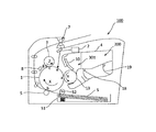
<画像形成装置の構成>
まず、図1を参照して、本発明の実施例(本実施例)に係る画像形成装置の構成及び画像形成動作について説明する。図1は、本実施例に係る画像形成装置の構成を示す概略断面図である。本実施例に係る画像形成装置100は、主な構成として、像担持体としての感光ドラム1、レーザビームスキャナ2、帯電部材としての帯電ローラ3、現像装置4、転写部材としての転写ローラ5、定着装置7を有している。
<Configuration of image forming apparatus>
First, the configuration and image forming operation of an image forming apparatus according to an embodiment of the present invention (this embodiment) will be described with reference to FIG. FIG. 1 is a schematic cross-sectional view showing the configuration of the image forming apparatus according to the present embodiment. An
画像形成装置100は、不図示のパーソナルコンピュータ等からの画像情報の信号を受け取り、装置下部に装着されたシートカセット51から搬送ローラ52によって記録材としてのシートSを搬送する。このシート搬送と同期して、感光ドラム1が回転駆動を開始する。感光ドラム1は、φ24mmの負極性OPC感光体である。この感光ドラム1は、図1中矢印X方向に周速100mm/sec(=プロセススピードPS、印字速度)の一定速度をもって回転駆動される。
The
帯電ローラ3は、感光ドラム1に接触して回転可能に設けられており、感光ドラム1表面を帯電する。帯電ローラ3は、導電性の弾性ローラであり、芯金と導電性弾性層からなり、感光ドラム1に対して所定の押圧力で圧接されている。感光ドラム1の表面うち帯電ローラ3と接触する位置を帯電領域cとする。この帯電領域cにおいて感光ドラム1表面は帯電ローラ3によって帯電される。
The charging
本実施例では、帯電ローラ3は図1中矢印Z方向に回転駆動する。帯電ローラ3には不図示の帯電電源により帯電バイアスが印加される。本実施例では帯電電源により帯電ローラ3の芯金に直流電圧を印加する。印加する直流電圧は、感光ドラム1の表面電位と帯電ローラ3の表面電位の電位差が放電開始電圧以上となるような値に設定されており、具体的には帯電バイアスとして−1300Vの直流電圧を印加している。このとき、感光ドラム1の表面を帯電電位(暗部電位)−700Vに一様に接触帯電させている。
In this embodiment, the charging
レーザビームスキャナ2は、レーザダイオード・ポリゴンミラー等を含む露光手段であって、帯電ローラ3により帯電された感光ドラム1表面を露光し静電潜像を形成する。レーザビームスキャナ2は、目的の画像情報の時系列電気ディジタル画素信号に対応して強度変調されたレーザ光を出力し、回転する感光ドラム1表面を走査露光する。感光ドラム
1をレーザ光で全面露光した場合、感光ドラム1面の電位が−150Vになるようにレーザーパワーは調整されている。
The
現像装置4には、本実施例では現像剤として磁性一成分現像剤(以下、単に、磁性トナーまたはトナーともいう)を使用している。構成によっては、非磁性でもよい。現像装置4は、磁性トナーを収容する現像剤収容部としての収容室200と、現像剤担持体としての現像ローラ13が配置された現像室301を有している。磁性トナーは、現像ローラ13に内包された磁界発生手段であるマグネットローラ14(図2参照)の磁力によって現像ローラ13に引きつけられる。
In the present embodiment, the developing
磁性トナーは、一定の摩擦帯電を帯び、現像バイアス印加電源により現像ローラ13と感光ドラム1との間に印加された現像バイアスにより、現像ローラ13上から感光ドラム1上(像担持体上)に移動する。感光ドラム1の表面のうち、現像ローラ13からトナーが移動してくる位置を現像領域aとする。現像ローラ13は、現像領域aにトナーを供給することにより、感光ドラム1上の静電潜像を現像し現像剤像としてのトナー像を形成する。なお、本実施例において現像バイアスは−350Vに設定されている。
The magnetic toner has a certain triboelectric charge, and from the developing
転写ローラ5は、感光ドラム1に対して圧接されている。感光ドラム1の表面のうち、転写ローラ5が圧接される位置を転写領域bとする。本実施例においては、芯金に中抵抗発泡層を形成した、ローラ抵抗値5×10⁸Ωの転写ローラ5を用いた。そして、芯金に+2.0kVの電圧を印加することで、感光ドラム1上に形成されたトナー像のシートS上(記録材上)への転写を行う。
The
定着装置7は熱定着方式の定着手段である。転写領域bを通過してトナー像が転写されたシートSは、感光ドラム1の表面から分離して、定着装置7へ導入される。そして、定着装置7において、トナー像がシートS上に加熱定着され、その後、シートSは画像形成物(プリントコピー)として装置外へ排出される。
The fixing device 7 is a heat fixing type fixing unit. The sheet S on which the toner image is transferred through the transfer region b is separated from the surface of the
<クリーナレスシステム>
ここで、クリーナレスシステムについて説明する。本実施例においては、転写工程後に感光ドラム1上に残留した転写残トナーを感光ドラム1上から除去するクリーニング部材を有さない、所謂クリーナレスシステムを採用する。転写工程後に感光ドラム1上に残留した転写残トナーは、感光ドラム1の回転方向Xにおける、帯電ローラ3と感光ドラム1との当接部(帯電領域c)の上流側の空隙部gに移動する。空隙部gでは、帯電ローラ3と感光ドラム1との間で放電が起きている。そのため、転写残トナーは放電によって感光ドラム1と同じ極性の負極性に帯電される。このとき、感光ドラム1の表面は−700Vに帯電されている。負極性に帯電した転写残トナーは、帯電領域cにおいて帯電ローラ3には付着せず通過することになる。感光ドラム1の表面電位=−700Vと帯電ローラ3の表面電位=−1300Vの電位差のためである。
<Cleanerless system>
Here, the cleanerless system will be described. In the present embodiment, a so-called cleanerless system is employed that does not have a cleaning member that removes transfer residual toner remaining on the
帯電領域cを通過した転写残トナーは、感光ドラム1の表面のうち、レーザビームスキャナ2によってレーザ光を照射されるレーザ照射位置eに到達する。転写残トナーは、レーザビームスキャナ2によるレーザ光を遮蔽するほど多くないため、感光ドラム1上の静電潜像を作像する工程に影響しない。レーザ照射位置eを通過したトナーは、現像領域aにおいて、非露光部(感光ドラム1の表面のうちレーザ照射を受けていない面)のトナーは、静電力によって現像ローラ13に回収される。
The untransferred toner that has passed through the charging region c reaches the laser irradiation position e on the surface of the
露光部(感光ドラム1の表面のうちレーザ照射を受けた面)のトナーは、静電力的には回収されずにそのまま感光ドラム1上に存在し続ける。しかし一部のトナーは、現像ローラ13と感光ドラム1の周速差による物理的な力で回収される。このように紙に転写され
ずに感光ドラム1上に残ったトナーは、概ね現像装置4に回収される。現像装置4に回収されたトナーは、現像装置4内に残っているトナーと混合され再利用される。
The toner on the exposed portion (the surface of the surface of the
本実施例では、転写残トナーを帯電ローラ3に付着させることなく帯電領域cを通過させるために、以下の2つの構成を採用している。1つ目は、感光ドラム1の回転方向における、転写領域bと帯電領域cとの間に除電部材としての光除電部材8を設けていることである。光除電部材8は、帯電領域cの上流側の空隙部gで安定した放電を行なうために、転写領域bを通過した後の感光ドラム1表面電位を光除電している。この光除電部材8によって、帯電前の感光ドラム1の電位を長手全域−150V程度にしておくことで、均一な放電が行なえ、転写残トナーを均一に負極性にすることが可能となる。
In this embodiment, the following two configurations are employed in order to pass the transfer residual toner through the charging region c without adhering to the charging
2つ目は、帯電ローラ3の周速と、感光ドラム1の周速とに所定の周速差を設け駆動回転させていることである。上述のように放電によって多くのトナーが負極性になるものの、若干負極性になりきれなかったトナーが残っており、このトナーが帯電領域cで帯電ローラ3に付着することがある。帯電ローラ3と感光ドラム1を所定の周速差を設けて駆動回転させることで、感光ドラム1と帯電ローラ3との摺擦によって、放電によって負極性になれなかったトナーを負極性にさせることが可能となる。そのため、トナーが帯電領域cで帯電ローラ3に付着してしまうことを抑制できる。
The second is that a predetermined peripheral speed difference is provided between the peripheral speed of the charging
本実施例においては、帯電ローラ3の芯金2aに帯電ローラギアが設けられており、帯電ローラギアは感光ドラム端部に設けられたドラムギアと係合している。よって、感光ドラム1が回転駆動するのに伴って、帯電ローラ3も回転駆動する。帯電ローラ3の周速は感光ドラム1の周速に対して早い、また遅くてもよい。さらには、帯電ローラ3と感光ドラム1は、順方向に回転するものでなくてもよく逆方向に回転するものであってもよい。
In this embodiment, a charging roller gear is provided on the metal core 2a of the charging
<現像装置の説明>
次に、図2を参照して、本実施例の現像装置の詳細を説明する。図2は、本実施例の現像装置の構成を示す概略断面図である。現像装置4は内部にトナーを収容するトナー収容室200と、トナーを感光ドラム1へ供給する現像室301を備えている。トナー収容室200にはトナーを現像室301へと搬送するための矢印E方向に回転可能な撹拌部材18、19が設けられている。現像室301は、前側(図2中左側)の下部に開口を有し、ここに現像剤担持体としての現像ローラ13が配設されている。
<Description of developing device>
Next, the details of the developing device of the present embodiment will be described with reference to FIG. FIG. 2 is a schematic cross-sectional view showing the configuration of the developing device of this embodiment. The developing
トナー収容室200に収容されるトナーとしては負帯電性の磁性一成分トナーが用いられる。このトナーは、結着樹脂(スチレン−n−ブチルアクリルレート共重合体)100重量部に、磁性体粒子80重量部を主成分として、ワックスなどを内包したもので、平均粒径は7.5μmである。また、外添剤としてシリカ微紛体1.2重量部を用いる。
As the toner stored in the
現像ローラ13は、アルミニウムやステンレススチールのパイプによって形成された非磁性スリーブの外周に厚み約500μmの導電性の弾性層を形成したものであり、現像室301を構成する枠体に矢印Y方向に回転自在に支持されている。現像ローラ13の表面は、所望量のトナーを担持し搬送することができるように、適切な表面粗さを有している。具体的には、現像ローラ13の表面粗さはJIS規格のRaで、周方向、長手方向での平均において、約2.5〜3.5μmとなるように形成されている。
The developing
また、現像ローラ13は、感光ドラム1に当接するように感光ドラム1の方向に押圧されている。現像ローラ13は、その長手方向(軸方向)の両端部に、侵入量規制コロが配設されており、これらのコロを感光ドラム1に当接させることにより、現像ローラ13と感光ドラム1表面との侵入量を所定の値になるようにしている。また、現像ローラ13の一方の端部には、現像ローラギヤが固定されており、この現像ローラギヤに画像形成装置
本体の駆動源から複数のギヤを介して駆動力が伝達され、現像ローラ13が回転駆動される。
Further, the developing
また、現像ローラ13の内側にはマグネットローラ14が配設されている。マグネットローラ14としては、円筒形状で、その周方向にN極とS極が交互に配置された4極マグネットロールを用いた。4極は、感光ドラム1対向部の現像極、後述する規制ブレード10の当接部に対向する規制極、現像室301のトナーを現像ローラ13に供給するための供給極、トナー吹出し防止シート17の対向部の漏れ防止極の4極である。各極の磁束密度は、規制極が一番強く70mT、その他が約50mTである。マグネットローラ14は、現像ローラ13が矢印Y方向に回転するのとは異なり、現像ローラ13の内側に固定的に配設されている。
A
上述の現像ローラ13表面には、電荷付与部材としての規制ブレード10が当接されている。規制ブレード10は、弾性部材15と、弾性部材15を支持し現像室301を構成する枠体に固定される支持板金16から構成されている。弾性部材15は、例えば、厚さ100μm程度のSUS(ステンレス鋼)やリン青銅等によって形成された板状のものであり、その基端部が支持板金16に固定されるとともに、その先端部が現像ローラ13表面に所定の圧力で当接されている。規制ブレード10の現像ローラ13に対する当接力は約20gf/cm〜40gf/cm(現像ローラ13の長手方向についての1cm当たりの当接荷重)となるように当接されている。本実施例では、規制ブレード10の自由端の先端部を現像ローラに当接させている。この規制ブレード10は、上述のマグネットローラ14の磁力によって現像ローラ13表面に引き付けられたトナーの厚層を規制するものである。上述したトナーを使用した場合、現像ローラ13上のトナーコート量は約0.4mg/cm2〜0.5mg/cm2程度である。
A regulating
現像ローラ13表面に担持されたトナーは、規制ブレード10によって層厚が規制される際の現像ローラ13と規制ブレード10間での摺擦による摩擦帯電により、適切な電荷が付与される。その後、電荷が付与されたトナーは、現像ローラ13の回転により現像領域aへと搬送される。このとき、現像ローラ13には、直流電源から現像バイアス(約−400V)が印加される。現像領域aにおいて、感光ドラム1の表面電位と現像ローラ13の表面電位の電位差によって、現像ローラ13上のトナーが、静電的に、感光ドラム1表面に形成された静電潜像に付着する。このようにして、静電潜像をトナー像として現像する。
The toner carried on the surface of the developing
<黒後カブリ>
次に、黒後カブリについて説明する。例えば、ベタ画像を形成する場合、現像ローラ13上のトナーは感光ドラム1上へほぼ100%移動する。ここで、ベタ画像形成直後の現像ローラに付着したトナーは、規制ブレード10によって1回しか摺擦されないため、十分な電荷付与がされない場合がある。十分に電荷付与されていないトナーは感光ドラム1の白地部に移動する現象が生じてしまう場合がある。このように、ベタ画像形成後に生じる感光ドラム1へのトナーの付着を黒後カブリという。黒後カブリは、印字直後に発生する現象であり、印字している時に発生することはない。黒後カブリは、印字パターンが現像ローラ13の1周分よりも短い場合は、その印字パターンの幅分生じるが、現像ローラ13の1周分以上の印字パターンの現像を行った場合は、黒後カブリが発生するのは現像ローラ13の1周分である。現像ローラ13が回転することで規制ブレード10によって2回以上摺擦された現像ローラ13上のトナーは、黒後カブリとして感光ドラム1上に移動しにくいためである(図6参照)。
<Black fogging>
Next, black post fogging will be described. For example, when forming a solid image, the toner on the developing
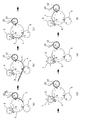
さらに、図3を参照して、黒後カブリの発生の詳細について説明する。図3は、現像ローラによる現像から回収までのトナーの動きの一例を示す模式図である。図3は、ベタ画
像を形成した直後に印字を行わない場合(白地となる場合)であって、現像ローラピッチと帯電ローラピッチの長さが同等の場合を一例として示したものである。ここで、現像ローラピッチとは、感光ドラム1表面に対する現像ローラ13の1周期分の長さをいい、帯電ローラピッチとは感光ドラム1表面に対する帯電ローラ3の1周期分の長さをいう。
Further, with reference to FIG. 3, the details of the occurrence of black post fogging will be described. FIG. 3 is a schematic diagram illustrating an example of toner movement from development to collection by the developing roller. FIG. 3 shows, as an example, a case where printing is not performed immediately after a solid image is formed (when the background is white), and the lengths of the developing roller pitch and the charging roller pitch are equal. Here, the developing roller pitch refers to the length of one cycle of the developing
現像ローラピッチ、帯電ローラピッチは、それぞれの外径と感光ドラム1に対する周速比(割合)で決定する。現像ローラ13の外径をHd、現像ローラ13の感光ドラム1に対する周速比をRdとすると、現像ローラピッチはHd×π/Rd×(感光ドラム1の周速)で表される(π:円周率)。また、帯電ローラ3の外径をHc、帯電ローラ3の感光ドラム1に対する周速比をRcとすると、帯電ローラピッチはHc×π/Rc×(感光ドラム1の周速)で表される。このことから、現像ローラピッチと帯電ローラピッチの関係は、Hd/RdとHc/Rcの関係と同等となる。
The developing roller pitch and the charging roller pitch are determined by the respective outer diameters and the peripheral speed ratio (ratio) to the
まず、図3(a)に示すように、現像領域aにおいて、現像ローラ13から感光ドラム1上にトナーTが現像される。現像直後の現像ローラ13上のトナーは、現像ローラ13の矢印Y方向の回転により、規制ブレード10によって1回だけ摺擦されて、現像領域aへと到達する。1回しか摺擦されておらず十分な電荷付与がされていないトナーは、現像領域aにおいて、現像ローラ13から感光ドラム1の白地部へ移動する。感光ドラム1上の白地部に移動したトナーを黒後カブリトナーtとする。このように感光ドラム1上の白地部に黒後カブリトナーtが付着することが上述した黒後カブリの発生である。なお、十分な電荷付与がされていない黒後カブリトナーtの極性は、図3(b)に示すように、正極性(+)、又は電荷がゼロとなっている。
First, as shown in FIG. 3A, the toner T is developed on the
黒後カブリトナーtは、感光ドラム1の矢印X方向の回転により、図3(b)に示すように、転写領域bへと到達する。転写領域bへと到達した黒後カブリトナーtは、転写ローラ5に印加されている正極の電圧により、正極性(+)に帯電する。
The black post fog toner t reaches the transfer region b as shown in FIG. 3B due to the rotation of the
正極に帯電した黒後カブリトナーtは、感光ドラム1の矢印X方向の回転により、図3(c)に示すように、転写領域bを通過し、帯電領域cに到達する。ここで、正極性に帯電している黒後カブリトナーtは、帯電ローラ3と感光ドラム1との間の空隙部gで放電されて負極性になる、又は帯電ローラ3と感光ドラム1との摺擦により負極性になる。ただし、黒後カブリトナーtの一部は、負極性に帯電されず、帯電領域cにおいて、感光ドラム1上から帯電ローラ3上(帯電ローラ上)へと移動する。その状態を図3(d)に示す。なお、図3(d)においては、負極性になって感光ドラム1上に残留する黒後カブリトナーの図示については省略している。負極性となって感光ドラム1上に残留する黒後カブリトナーは、感光ドラム1の回転により、現像領域aに到達し、現像ローラ13に回収され、再利用される。
The post-black fog toner t charged on the positive electrode passes through the transfer area b and reaches the charging area c as shown in FIG. 3C due to the rotation of the
帯電ローラ3上に付着した黒後カブリトナーtは、帯電ローラ3の矢印Z方向の回転により、帯電領域cに戻ってくる。そして、帯電領域cに戻ってきた黒後カブリトナーtは、帯電ローラ3と感光ドラム1との間の空隙部gで放電されて負極性になる、又は帯電ローラ3と感光ドラム1との摺擦により負極性になる。負極性に帯電された黒後カブリトナーtは、図3(e)、(f)に示すように、帯電ローラ3上から感光ドラム1上へ移動する。感光ドラム1へ移動した黒後カブリトナーtは、感光ドラム1の矢印X方向の回転により、現像領域aへと戻ってくる。そして、黒後カブリトナーtは、現像ローラ13に回収され、再利用される。
The post-black fog toner t adhering to the charging
さらに、黒後カブリの発生を原因とする帯電ムラについて説明する。帯電ローラ3へ付着した黒後カブリトナーが、帯電ローラ3の回転により再び帯電領域cに到達した際、感光ドラム1上に黒後カブリが存在している場合、帯電不良が生じてしまう。上述したよう
に、帯電ローラ3へ付着した黒後カブリトナーは、帯電領域cで再び感光ドラム1へと移動する。その際、感光ドラム1上にも黒後カブリトナーが付着していると、帯電ローラ3と感光ドラム1との間の空隙部gでの放電が十分にされず、また帯電ローラ3と感光ドラム1によって十分な摺擦されない場合がある。そのため、帯電ローラ3上の黒後カブリトナーは、帯電領域cに到達しても、感光ドラム1へと移動することができず、帯電ローラ3上に付着したままとなってしまう。また逆に感光ドラム1上の黒後カブリトナーがさらに帯電ローラ3上に付着してしまう場合もある。そのように帯電ローラ3上に黒後カブリトナーが付着していると、帯電ローラ3による感光ドラム1に対する帯電が均等にされず、帯電にムラが生じてしまう。
Further, charging unevenness caused by the occurrence of fogging after black will be described. When the post-black fog toner adhering to the charging
(実施例1)
次に、実施例1について説明する。実施例1の構成においては、帯電ローラ3上に付着した黒後カブリトナーを原因とする帯電ムラを抑制することができる。実施例1においては、現像ローラピッチと帯電ローラピッチを同等とした。すなわち、Hc/Rc=Hd/Rdとした。具体的には、実施例1においては、現像ローラ13の外径Hd=φ12mm、現像ローラ13の感光ドラム1に対する周速比Rd=120%とした。また、帯電ローラ3の外径Hc=φ9mm、帯電ローラ3の感光ドラム1に対する周速比Rc=90%とした。
(Example 1)
Next, Example 1 will be described. In the configuration of the first embodiment, charging unevenness caused by the black post fog toner adhering to the charging
実施例1においては、まず、1回目の黒後カブリが発生し、その黒後カブリトナーが、感光ドラム1の回転により、帯電領域cに到達する。その際、放電、摺擦で電荷付与が十分にされなかった黒後カブリトナーの一部が帯電ローラ3に付着する。その後、帯電ローラ3の回転により、帯電ローラ3に付着した黒後カブリトナーは、再び帯電領域cに到達する。
In the first embodiment, first black post fogging occurs, and the black post fog toner reaches the charging region c by the rotation of the
実施例1の構成において、帯電ローラ3上の黒後カブリトナーが再び帯電領域cに到達した際、感光ドラム1上に、黒後カブリトナーは存在していない。実施例1においては、現像ローラピッチと帯電ローラピッチが同じため、黒後カブリトナーの先端部が再び帯電領域cに到達する直前に、黒後カブリトナーの後端部が帯電領域cで帯電ローラ3に付着することとなる。実施例1においては、帯電ローラピッチと現像ローラピッチが同等であるため、帯電ローラ3表面の同じ部分に連続的に黒後カブリがくることがないため、付着と回復を繰り返すことが可能となる。
In the configuration of the first exemplary embodiment, when the post-black fog toner on the charging
本実施例においては、黒後カブリの長さが、印字の長さ、又は現像ローラピッチと同じであることを前提として説明したが、そうでない場合もある。例えば、黒後カブリはある程度の長さ現像しないと発生しないことが分かっている。この理由としては、一つには現像した部分と前後の現像していない部分が規制ブレード10で層厚規制される際に電荷保持しているトナーが混ざるためである。そして、二つ目には規制ブレード10との当接部上流に、層厚規制された際に残された電荷を保持するトナーが存在するためである。このように黒後カブリが発生しない幅は規制ブレード10の姿勢や当接圧、さらには先端形状(段差形状による取り込み部等)、また現像ローラ13に担持されるトナーコート量によって異なる。例えば、先端部で約0.8mm、後端部で約0.5mm程度黒後カブリが発生しないような場合がある。そのような場合、帯電ローラピッチと現像ローラピッチが約1.3mm以内でずれていても同等の効果が得られる。
In the present embodiment, the description has been made on the assumption that the length of the post-black fog is the same as the printing length or the developing roller pitch. For example, it has been found that after-black fog does not occur unless developed for a certain length. One reason for this is that, when the layer thickness is regulated by the regulating
(実施例2)
次に、実施例2について説明する。実施例2においては、帯電ローラピッチを現像ローラピッチよりも長くした。すなわち、Hc/Rc>Hd/Rdとした。具体的には、実施例2においては、現像ローラ13の外径Hd=φ12mm、現像ローラ13の感光ドラム1に対する周速比Rd=140%とした。また、帯電ローラ3の外径Hc=φ9mm、帯
電ローラ3の感光ドラム1に対する周速比Rc=90%とした。
(Example 2)
Next, Example 2 will be described. In Example 2, the charging roller pitch was made longer than the developing roller pitch. That is, Hc / Rc> Hd / Rd. Specifically, in Example 2, the outer diameter Hd of the developing
帯電ローラピッチが長い場合には、現像ローラ13の1周分の黒後カブリトナーが発生した場合でも、帯電ローラ3全周にトナーが付着することはない。すなわち、帯電ローラ3に付着した黒後カブリトナーの先端部が帯電領域cに再び到達した際、黒後カブリトナーの後端部は帯電ローラ3上にある。そのため、帯電ローラ3に付着した黒後カブリトナーは、帯電領域cに到達すると、放電、摺擦により電荷が付与され、感光ドラム1上に戻ることとなる。
When the charging roller pitch is long, the toner does not adhere to the entire circumference of the charging
しかしながら、Hc/Rc>Hd/Rdの関係を満たす場合であっても、印字パターンが帯電ローラピッチで連続印字される場合は、帯電ムラが生じてしまうおそれがある。図4を参照して、Hc/Rc>Hd/Rdの関係を満たす場合であっても、帯電ムラが生じてしまう場合について説明する。図4(a)は感光ドラム表面の状態を示す図であり、図4(b)は帯電ローラ表面の状態を示す図である。 However, even when the relationship of Hc / Rc> Hd / Rd is satisfied, if the print pattern is continuously printed at the charging roller pitch, charging unevenness may occur. With reference to FIG. 4, the case where uneven charging occurs even when the relationship of Hc / Rc> Hd / Rd is satisfied will be described. FIG. 4A is a diagram illustrating the state of the surface of the photosensitive drum, and FIG. 4B is a diagram illustrating the state of the surface of the charging roller.
図4(a)において、帯電ローラピッチが現像ローラピッチの3倍である。そして、印字パターンが、現像ローラピッチの1周分の印字、現像ローラピッチ1周分の白地、現像ローラの1周分の白地、を繰り返す。このような場合、図4(b)に示すように、帯電ローラ3上に付着した黒後カブリトナーが帯電領域cに戻ってきたとき、感光ドラム1上の帯電領域cに次の黒後カブリトナーが到達する。そのため、黒後カブリトナーが帯電領域cで重なり、さらに帯電ローラ3の表面が汚れてしまう。すなわち、3(Hd/Rd)≧Hc/Rc≧Hd/Rdを満たす場合は、帯電ローラ3の表面の汚れは発生しにくいと考えられる。以上説明したように、実施例2の構成においては、印字パターンによっては帯電不良が生じる場合もある。ただし、そのような印字パターンとなるのは稀である。
In FIG. 4A, the charging roller pitch is three times the developing roller pitch. The print pattern repeats printing for one development roller pitch, white background for one development roller pitch, and white background for one development roller pitch. In such a case, as shown in FIG. 4B, when the post-black fog toner adhering on the charging
さらに、図5を参照して、実施例1,2と比較例について説明する。図5は、感光ドラム表面の状態と帯電ローラ表面の状態を示す図である。図5(a)は、黒後カブリが現像ローラの1周分(現像ローラピッチ分)発生した場合における、感光ドラム1表面の状態を示す図である。図5(b)〜図5(d)は、黒後カブリが現像ローラの1周分(現像ローラピッチ分)発生した場合における、帯電ローラの表面の状態を示す図である。上述したように、実施例1においては、帯電ローラピッチと現像ローラピッチを同等とし、実施例2においては、帯電ローラピッチを現像ローラピッチよりも長くした。
Furthermore, Examples 1 and 2 and a comparative example will be described with reference to FIG. FIG. 5 is a diagram illustrating the state of the photosensitive drum surface and the state of the charging roller surface. FIG. 5A is a diagram illustrating a state of the surface of the
図5(b)に示すように、実施例1においては、帯電ローラ3上に付着した黒後カブリトナーが、帯電ローラ3が1周することにより再び帯電領域cに戻ってきた際に、感光ドラム1上に黒後カブリが存在しない。そのため、帯電ムラは生じない。同じく、図5(c)に示すように、実施例2においても、帯電ローラ3上に付着した黒後カブリトナーが、帯電ローラ3が1周することにより再び帯電領域cに戻ってきた際に、感光ドラム1上に黒後カブリが存在しない。そのため、帯電ムラは生じない。
As shown in FIG. 5B, in the first embodiment, when the black post fog toner adhering to the charging
ここで、比較例においては、帯電ローラピッチを現像ローラピッチよりも短くした。すなわち、Hc/Rc<Hd/Rdとした。具体的には、比較例においては、現像ローラ13の外径Hd=φ12mm、現像ローラ13の感光ドラム1に対する周速比Rd=120%とした。また、帯電ローラ3の外径Hc=φ9mm、帯電ローラ3の感光ドラム1に対する周速比Rc=130%とした。
Here, in the comparative example, the charging roller pitch is shorter than the developing roller pitch. That is, Hc / Rc <Hd / Rd. Specifically, in the comparative example, the outer diameter Hd of the developing
図5(d)に示すように、帯電ローラピッチが現像ローラピッチ(黒後カブリの長さ)よりも短い場合、帯電ローラ3上に付着した黒後カブリトナーが再び帯電領域cに戻ってきた際、感光ドラム1上にも黒後カブリトナーが存在している。そのため、帯電ローラ3上の黒後カブリトナーと、感光ドラム1上の黒後カブリトナーとが同じタイミングで帯電
領域cに到達することとなり重なり合ってしまう。そのため、帯電ローラ3の1周目に付着した黒後カブリトナーを放電・摺擦により感光ドラム1表面に戻すことができない以上に更にトナーが帯電ローラ3上に付着してしまう場合がある。このように連続的に帯電ローラ3に黒後カブリトナーが付着してしまうと、帯電性能が低下し所望の電位に感光ドラム1表面を帯電できない。その結果、帯電ムラが発生してしまうこととなる。
As shown in FIG. 5D, when the charging roller pitch is shorter than the developing roller pitch (the length of the black post fog), the black post fog toner adhered on the charging
上記実施例1、2、比較例からわかるように、帯電ローラピッチを現像ローラピッチ以上とすることで、帯電ムラを効果的に抑制することが可能となる。最も望ましくは、実施例1で説明したように帯電ローラピッチと現像ローラピッチと略同等にすることがよい。なお、Hc/Rc≧Hd/Rdであれば、本発明の効果を得ることができるが、Hc/RcはHd/Rdの3倍以下であることが好ましい。すなわち、3(Hd/Rd)≧Hc/Rc≧Hd/Rdを満たすことが好ましい。また、実施例1、2では、磁性一成分トナーを用いた接触式の現像装置4を採用しているが、この限りでなく、非磁性一成分トナーを用いた接触現像装置においても、黒後カブリが発生する場合においては同様の効果が得られる。
As can be seen from Examples 1 and 2 and the comparative example, the charging unevenness can be effectively suppressed by setting the charging roller pitch to be equal to or larger than the developing roller pitch. Most preferably, as described in the first embodiment, the charging roller pitch and the developing roller pitch should be approximately equal. If Hc / Rc ≧ Hd / Rd, the effects of the present invention can be obtained, but Hc / Rc is preferably 3 times or less of Hd / Rd. That is, it is preferable to satisfy 3 (Hd / Rd) ≧ Hc / Rc ≧ Hd / Rd. In the first and second embodiments, the contact-
1…感光ドラム(像担持体)、3…帯電ローラ(帯電部材)、9…現像ローラ(現像剤担持体)、10…規制ブレード(電荷付与部材)、100…画像形成装置
DESCRIPTION OF
上記目的を達成するために本発明に係る画像形成装置は、
回転可能な像担持体と、
前記像担持体に接触して回転可能に設けられ、前記像担持体を帯電する帯電部材と、
前記像担持体に接触して回転可能に設けられ、前記像担持体上に現像剤を供給する現像剤担持体であって、前記像担持体上に形成された現像剤像が記録材上に転写された後に前記像担持体上に残留した現像剤を回収する現像剤担持体と、
を有し、
前記帯電部材の外径をHcとし、
前記像担持体の周速に対する前記帯電部材の周速の割合をRcとし、
前記現像剤担持体の外径をHdとし、
前記像担持体の周速に対する前記現像剤担持体の周速の割合をRdとした場合、
Hc/Rc≧Hd/Rd
を満たすことを特徴とする。
In order to achieve the above object, an image forming apparatus according to the present invention includes:
A rotatable image carrier;
A charging member which is rotatably provided in contact with the image carrier and charges the image carrier;
The image carrier contact rotatably provided on the image a bearing member to the developer for supplying developer carrier before the developer image formed on the Kizo bearing member onto the recording material a developer carrying member for collecting the developer remaining on the image bearing member after being transferred to,
Have,
The outer diameter of the charging member is Hc,
The ratio of the peripheral speed of the charging member to the peripheral speed of the image carrier is Rc,
The outer diameter of the developer carrier is Hd,
When the ratio of the peripheral speed of the developer carrier to the peripheral speed of the image carrier is Rd,
Hc / Rc ≧ Hd / Rd
It is characterized by satisfying.
Claims (10)
前記像担持体に接触して回転可能に設けられ、前記像担持体を帯電する帯電部材と、
前記像担持体に接触して回転可能に設けられ、前記像担持体上に現像剤を供給する現像剤担持体であって、現像剤が供給されることにより前記像担持体上に形成された現像剤像が記録材上に転写された後に前記像担持体上に残留した現像剤を回収する現像剤担持体と、
前記現像剤担持体から前記像担持体へ現像剤が供給されるように現像剤に電荷を付与する電荷付与部材と、
を有し、
前記帯電部材の外径をHcとし、
前記像担持体の周速に対する前記帯電部材の周速の割合をRcとし、
前記現像剤担持体の外径をHdとし、
前記像担持体の周速に対する前記現像剤担持体の周速の割合をRdとした場合、
Hc/Rc≧Hd/Rd
を満たすことを特徴とする画像形成装置。 A rotatable image carrier;
A charging member which is rotatably provided in contact with the image carrier and charges the image carrier;
A developer carrier that is rotatably provided in contact with the image carrier and supplies a developer onto the image carrier, and is formed on the image carrier by being supplied with the developer. A developer carrier for recovering the developer remaining on the image carrier after the developer image is transferred onto the recording material;
A charge imparting member that imparts a charge to the developer such that the developer is supplied from the developer carrier to the image carrier;
Have
The outer diameter of the charging member is Hc,
The ratio of the peripheral speed of the charging member to the peripheral speed of the image carrier is Rc,
The outer diameter of the developer carrier is Hd,
When the ratio of the peripheral speed of the developer carrier to the peripheral speed of the image carrier is Rd,
Hc / Rc ≧ Hd / Rd
An image forming apparatus characterized by satisfying the above.
前記現像剤担持体により前記静電潜像へ現像剤が供給されることにより前記像担持体上に形成された現像剤像を記録材上に転写する転写部材と、
を有することを特徴とする請求項1乃至7のいずれか1項に記載の画像形成装置。 Exposure means for exposing the image carrier charged by the charging member to form an electrostatic latent image on the image carrier;
A transfer member for transferring a developer image formed on the image carrier by supplying the developer to the electrostatic latent image by the developer carrier;
The image forming apparatus according to claim 1, further comprising:
Priority Applications (5)
| Application Number | Priority Date | Filing Date | Title |
|---|---|---|---|
| JP2014122463A JP2016004070A (en) | 2014-06-13 | 2014-06-13 | Image forming apparatus |
| US14/733,082 US9547273B2 (en) | 2014-06-13 | 2015-06-08 | Image forming apparatus having simultaneous development and cleaning |
| CN201510312651.9A CN105319899B (en) | 2014-06-13 | 2015-06-09 | Image forming apparatus with a toner supply device |
| EP15171579.4A EP2955583B1 (en) | 2014-06-13 | 2015-06-11 | Image forming apparatus |
| KR1020150083319A KR101811101B1 (en) | 2014-06-13 | 2015-06-12 | Image forming apparatus |
Applications Claiming Priority (1)
| Application Number | Priority Date | Filing Date | Title |
|---|---|---|---|
| JP2014122463A JP2016004070A (en) | 2014-06-13 | 2014-06-13 | Image forming apparatus |
Publications (2)
| Publication Number | Publication Date |
|---|---|
| JP2016004070A true JP2016004070A (en) | 2016-01-12 |
| JP2016004070A5 JP2016004070A5 (en) | 2017-07-27 |
Family
ID=53373355
Family Applications (1)
| Application Number | Title | Priority Date | Filing Date |
|---|---|---|---|
| JP2014122463A Pending JP2016004070A (en) | 2014-06-13 | 2014-06-13 | Image forming apparatus |
Country Status (5)
| Country | Link |
|---|---|
| US (1) | US9547273B2 (en) |
| EP (1) | EP2955583B1 (en) |
| JP (1) | JP2016004070A (en) |
| KR (1) | KR101811101B1 (en) |
| CN (1) | CN105319899B (en) |
Families Citing this family (2)
| Publication number | Priority date | Publication date | Assignee | Title |
|---|---|---|---|---|
| EP3523714A1 (en) | 2016-10-10 | 2019-08-14 | Volkswagen Aktiengesellschaft | Method for adapting the presentation and use of a graphical user interface |
| US10234806B2 (en) | 2017-02-23 | 2019-03-19 | Canon Kabushiki Kaisha | Image forming apparatus |
Citations (6)
| Publication number | Priority date | Publication date | Assignee | Title |
|---|---|---|---|---|
| JPH05210300A (en) * | 1991-10-30 | 1993-08-20 | Oki Electric Ind Co Ltd | Image forming device and method |
| JPH10213945A (en) * | 1997-01-29 | 1998-08-11 | Canon Inc | Image forming device and process cartridge |
| JP2000122377A (en) * | 1998-10-09 | 2000-04-28 | Canon Inc | Image forming device and electrification member |
| JP2003156925A (en) * | 2001-11-22 | 2003-05-30 | Canon Inc | Frictional-electrification evaluating method and electrophotographic method |
| US6649315B1 (en) * | 1998-08-27 | 2003-11-18 | Nippon Zeon Co., Ltd. | Nonmagnetic one component developer and developing method |
| JP2006154093A (en) * | 2004-11-26 | 2006-06-15 | Canon Inc | Magnetic toner, development method, image forming method, development apparatus, electrophotographic cartridge, and electrophotographic image forming apparatus |
Family Cites Families (22)
| Publication number | Priority date | Publication date | Assignee | Title |
|---|---|---|---|---|
| US4967231A (en) * | 1987-12-29 | 1990-10-30 | Kabushiki Kaisha Toshiba | Apparatus for forming an electrophotographic latent image |
| JP2987254B2 (en) * | 1992-05-29 | 1999-12-06 | 株式会社東芝 | Developing device and image forming device |
| DE69418268T2 (en) * | 1993-09-07 | 1999-09-23 | Matsushita Electric Ind Co Ltd | Charger and imaging device with the charger |
| DE69721607T2 (en) * | 1996-02-20 | 2004-03-18 | Canon K.K. | Image forming method |
| EP0844536B1 (en) * | 1996-11-26 | 2004-05-06 | Canon Kabushiki Kaisha | Image forming method |
| DE69818124T2 (en) | 1997-03-05 | 2004-07-15 | Canon K.K. | Charging device, charging method, cassette and image forming apparatus |
| US6118965A (en) * | 1997-10-20 | 2000-09-12 | Canon Kabushiki Kaisha | Image forming apparatus having a contact-type charger |
| JP3502554B2 (en) * | 1998-02-04 | 2004-03-02 | シャープ株式会社 | Developing device |
| JP4298114B2 (en) * | 2000-02-21 | 2009-07-15 | キヤノン株式会社 | Developer, image forming method using the developer, and process cartridge |
| CA2337087C (en) * | 2000-03-08 | 2006-06-06 | Canon Kabushiki Kaisha | Magnetic toner, process for production thereof, and image forming method, apparatus and process cartridge using the toner |
| JP3647409B2 (en) * | 2000-10-20 | 2005-05-11 | キヤノン株式会社 | Charging device, process cartridge, image forming apparatus, roller-shaped charging member |
| US6553199B2 (en) | 2000-10-20 | 2003-04-22 | Canon Kabushiki Kaisha | Charging device, process cartridge and image forming apparatus |
| EP1207429B1 (en) * | 2000-11-15 | 2007-02-07 | Canon Kabushiki Kaisha | Image forming method and apparatus |
| JP3728267B2 (en) * | 2002-04-23 | 2005-12-21 | キヤノン株式会社 | Process cartridge and image forming apparatus |
| JP3793192B2 (en) | 2002-10-25 | 2006-07-05 | キヤノン株式会社 | Image forming apparatus |
| JP2005156654A (en) | 2003-11-21 | 2005-06-16 | Canon Inc | Charging device, process cartridge, and image forming apparatus |
| JP4510493B2 (en) | 2004-03-29 | 2010-07-21 | キヤノン株式会社 | Image forming apparatus |
| JP6099893B2 (en) * | 2012-07-10 | 2017-03-22 | キヤノン株式会社 | Image forming apparatus |
| JP6112794B2 (en) * | 2012-07-10 | 2017-04-12 | キヤノン株式会社 | Image forming apparatus |
| EP2908179B1 (en) * | 2014-02-18 | 2020-08-12 | Canon Kabushiki Kaisha | Developing apparatus, cartridge, and image forming apparatus |
| JP6624802B2 (en) * | 2014-06-13 | 2019-12-25 | キヤノン株式会社 | Image forming device |
| JP6602002B2 (en) * | 2014-08-22 | 2019-11-06 | キヤノン株式会社 | Image forming apparatus |
-
2014
- 2014-06-13 JP JP2014122463A patent/JP2016004070A/en active Pending
-
2015
- 2015-06-08 US US14/733,082 patent/US9547273B2/en active Active
- 2015-06-09 CN CN201510312651.9A patent/CN105319899B/en active Active
- 2015-06-11 EP EP15171579.4A patent/EP2955583B1/en active Active
- 2015-06-12 KR KR1020150083319A patent/KR101811101B1/en active IP Right Grant
Patent Citations (6)
| Publication number | Priority date | Publication date | Assignee | Title |
|---|---|---|---|---|
| JPH05210300A (en) * | 1991-10-30 | 1993-08-20 | Oki Electric Ind Co Ltd | Image forming device and method |
| JPH10213945A (en) * | 1997-01-29 | 1998-08-11 | Canon Inc | Image forming device and process cartridge |
| US6649315B1 (en) * | 1998-08-27 | 2003-11-18 | Nippon Zeon Co., Ltd. | Nonmagnetic one component developer and developing method |
| JP2000122377A (en) * | 1998-10-09 | 2000-04-28 | Canon Inc | Image forming device and electrification member |
| JP2003156925A (en) * | 2001-11-22 | 2003-05-30 | Canon Inc | Frictional-electrification evaluating method and electrophotographic method |
| JP2006154093A (en) * | 2004-11-26 | 2006-06-15 | Canon Inc | Magnetic toner, development method, image forming method, development apparatus, electrophotographic cartridge, and electrophotographic image forming apparatus |
Also Published As
| Publication number | Publication date |
|---|---|
| KR20150143355A (en) | 2015-12-23 |
| EP2955583A1 (en) | 2015-12-16 |
| KR101811101B1 (en) | 2017-12-20 |
| US20150362886A1 (en) | 2015-12-17 |
| CN105319899B (en) | 2020-02-18 |
| US9547273B2 (en) | 2017-01-17 |
| EP2955583B1 (en) | 2020-05-13 |
| CN105319899A (en) | 2016-02-10 |
Similar Documents
| Publication | Publication Date | Title |
|---|---|---|
| JP5968480B1 (en) | Image forming apparatus | |
| JP6602002B2 (en) | Image forming apparatus | |
| JPH09288426A (en) | Image forming device | |
| JP5121216B2 (en) | Image forming apparatus | |
| KR101811101B1 (en) | Image forming apparatus | |
| JP2009151119A (en) | Image forming apparatus | |
| JP2007065591A (en) | Image forming apparatus | |
| JP2014102341A (en) | Developing apparatus and image forming apparatus | |
| JP2018013710A (en) | Image forming apparatus, process cartridge, development cartridge and drum cartridge | |
| JP6843556B2 (en) | Image forming device | |
| JP2005092146A (en) | Image forming apparatus, electrifying member, electrifying device, cleaning means and process cartridge | |
| JP7183029B2 (en) | Cleaning device, cartridge and image forming device | |
| JP3018805B2 (en) | Electrophotographic equipment | |
| JP2003228264A (en) | Cleaner and image forming apparatus with the same | |
| JP2016109737A (en) | Image forming apparatus | |
| JP6632292B2 (en) | Image forming device | |
| JP2017207530A (en) | Image forming apparatus and process cartridge | |
| JP6685676B2 (en) | Developing device, process cartridge and image forming device | |
| JP2019159108A (en) | Electrifying device, process cartridge, and image forming apparatus | |
| JP2008015148A (en) | Image forming apparatus | |
| JP2004109221A (en) | Image forming apparatus | |
| KR20080053749A (en) | Image forming apparatus | |
| JPS63205685A (en) | Image forming device | |
| JP2001356590A (en) | Image forming device and developing device | |
| JP2016167054A (en) | Charging device, process cartridge, and image forming apparatus |
Legal Events
| Date | Code | Title | Description |
|---|---|---|---|
| A521 | Request for written amendment filed |
Free format text: JAPANESE INTERMEDIATE CODE: A523 Effective date: 20170613 |
|
| A621 | Written request for application examination |
Free format text: JAPANESE INTERMEDIATE CODE: A621 Effective date: 20170613 |
|
| A977 | Report on retrieval |
Free format text: JAPANESE INTERMEDIATE CODE: A971007 Effective date: 20180223 |
|
| A131 | Notification of reasons for refusal |
Free format text: JAPANESE INTERMEDIATE CODE: A131 Effective date: 20180306 |
|
| A521 | Request for written amendment filed |
Free format text: JAPANESE INTERMEDIATE CODE: A523 Effective date: 20180507 |
|
| A02 | Decision of refusal |
Free format text: JAPANESE INTERMEDIATE CODE: A02 Effective date: 20180731 |
|
| RD02 | Notification of acceptance of power of attorney |
Free format text: JAPANESE INTERMEDIATE CODE: A7422 Effective date: 20181116 |