JP2015537377A - Heat sink mounting apparatus and method - Google Patents
Heat sink mounting apparatus and method Download PDFInfo
- Publication number
- JP2015537377A JP2015537377A JP2015537844A JP2015537844A JP2015537377A JP 2015537377 A JP2015537377 A JP 2015537377A JP 2015537844 A JP2015537844 A JP 2015537844A JP 2015537844 A JP2015537844 A JP 2015537844A JP 2015537377 A JP2015537377 A JP 2015537377A
- Authority
- JP
- Japan
- Prior art keywords
- circuit board
- electronic device
- shield
- heat sink
- tab
- Prior art date
- Legal status (The legal status is an assumption and is not a legal conclusion. Google has not performed a legal analysis and makes no representation as to the accuracy of the status listed.)
- Withdrawn
Links
Images


Classifications
-
- H—ELECTRICITY
- H05—ELECTRIC TECHNIQUES NOT OTHERWISE PROVIDED FOR
- H05K—PRINTED CIRCUITS; CASINGS OR CONSTRUCTIONAL DETAILS OF ELECTRIC APPARATUS; MANUFACTURE OF ASSEMBLAGES OF ELECTRICAL COMPONENTS
- H05K7/00—Constructional details common to different types of electric apparatus
- H05K7/20—Modifications to facilitate cooling, ventilating, or heating
- H05K7/2039—Modifications to facilitate cooling, ventilating, or heating characterised by the heat transfer by conduction from the heat generating element to a dissipating body
- H05K7/20409—Outer radiating structures on heat dissipating housings, e.g. fins integrated with the housing
-
- G—PHYSICS
- G06—COMPUTING; CALCULATING OR COUNTING
- G06F—ELECTRIC DIGITAL DATA PROCESSING
- G06F1/00—Details not covered by groups G06F3/00 - G06F13/00 and G06F21/00
- G06F1/16—Constructional details or arrangements
- G06F1/20—Cooling means
-
- G—PHYSICS
- G06—COMPUTING; CALCULATING OR COUNTING
- G06F—ELECTRIC DIGITAL DATA PROCESSING
- G06F1/00—Details not covered by groups G06F3/00 - G06F13/00 and G06F21/00
- G06F1/16—Constructional details or arrangements
- G06F1/18—Packaging or power distribution
- G06F1/181—Enclosures
-
- G—PHYSICS
- G06—COMPUTING; CALCULATING OR COUNTING
- G06F—ELECTRIC DIGITAL DATA PROCESSING
- G06F1/00—Details not covered by groups G06F3/00 - G06F13/00 and G06F21/00
- G06F1/16—Constructional details or arrangements
- G06F1/18—Packaging or power distribution
- G06F1/183—Internal mounting support structures, e.g. for printed circuit boards, internal connecting means
-
- H—ELECTRICITY
- H01—ELECTRIC ELEMENTS
- H01L—SEMICONDUCTOR DEVICES NOT COVERED BY CLASS H10
- H01L23/00—Details of semiconductor or other solid state devices
- H01L23/34—Arrangements for cooling, heating, ventilating or temperature compensation ; Temperature sensing arrangements
- H01L23/40—Mountings or securing means for detachable cooling or heating arrangements ; fixed by friction, plugs or springs
- H01L23/4093—Snap-on arrangements, e.g. clips
-
- H—ELECTRICITY
- H05—ELECTRIC TECHNIQUES NOT OTHERWISE PROVIDED FOR
- H05K—PRINTED CIRCUITS; CASINGS OR CONSTRUCTIONAL DETAILS OF ELECTRIC APPARATUS; MANUFACTURE OF ASSEMBLAGES OF ELECTRICAL COMPONENTS
- H05K7/00—Constructional details common to different types of electric apparatus
- H05K7/02—Arrangements of circuit components or wiring on supporting structure
- H05K7/12—Resilient or clamping means for holding component to structure
-
- H—ELECTRICITY
- H05—ELECTRIC TECHNIQUES NOT OTHERWISE PROVIDED FOR
- H05K—PRINTED CIRCUITS; CASINGS OR CONSTRUCTIONAL DETAILS OF ELECTRIC APPARATUS; MANUFACTURE OF ASSEMBLAGES OF ELECTRICAL COMPONENTS
- H05K7/00—Constructional details common to different types of electric apparatus
- H05K7/20—Modifications to facilitate cooling, ventilating, or heating
- H05K7/2039—Modifications to facilitate cooling, ventilating, or heating characterised by the heat transfer by conduction from the heat generating element to a dissipating body
- H05K7/20436—Inner thermal coupling elements in heat dissipating housings, e.g. protrusions or depressions integrally formed in the housing
- H05K7/2049—Pressing means used to urge contact, e.g. springs
-
- H—ELECTRICITY
- H05—ELECTRIC TECHNIQUES NOT OTHERWISE PROVIDED FOR
- H05K—PRINTED CIRCUITS; CASINGS OR CONSTRUCTIONAL DETAILS OF ELECTRIC APPARATUS; MANUFACTURE OF ASSEMBLAGES OF ELECTRICAL COMPONENTS
- H05K9/00—Screening of apparatus or components against electric or magnetic fields
-
- H—ELECTRICITY
- H05—ELECTRIC TECHNIQUES NOT OTHERWISE PROVIDED FOR
- H05K—PRINTED CIRCUITS; CASINGS OR CONSTRUCTIONAL DETAILS OF ELECTRIC APPARATUS; MANUFACTURE OF ASSEMBLAGES OF ELECTRICAL COMPONENTS
- H05K9/00—Screening of apparatus or components against electric or magnetic fields
- H05K9/0007—Casings
- H05K9/002—Casings with localised screening
- H05K9/0022—Casings with localised screening of components mounted on printed circuit boards [PCB]
- H05K9/0024—Shield cases mounted on a PCB, e.g. cans or caps or conformal shields
- H05K9/0032—Shield cases mounted on a PCB, e.g. cans or caps or conformal shields having multiple parts, e.g. frames mating with lids
-
- H—ELECTRICITY
- H01—ELECTRIC ELEMENTS
- H01L—SEMICONDUCTOR DEVICES NOT COVERED BY CLASS H10
- H01L23/00—Details of semiconductor or other solid state devices
- H01L23/34—Arrangements for cooling, heating, ventilating or temperature compensation ; Temperature sensing arrangements
- H01L23/36—Selection of materials, or shaping, to facilitate cooling or heating, e.g. heatsinks
- H01L23/367—Cooling facilitated by shape of device
- H01L23/3672—Foil-like cooling fins or heat sinks
-
- H—ELECTRICITY
- H01—ELECTRIC ELEMENTS
- H01L—SEMICONDUCTOR DEVICES NOT COVERED BY CLASS H10
- H01L2924/00—Indexing scheme for arrangements or methods for connecting or disconnecting semiconductor or solid-state bodies as covered by H01L24/00
- H01L2924/0001—Technical content checked by a classifier
- H01L2924/0002—Not covered by any one of groups H01L24/00, H01L24/00 and H01L2224/00
-
- Y—GENERAL TAGGING OF NEW TECHNOLOGICAL DEVELOPMENTS; GENERAL TAGGING OF CROSS-SECTIONAL TECHNOLOGIES SPANNING OVER SEVERAL SECTIONS OF THE IPC; TECHNICAL SUBJECTS COVERED BY FORMER USPC CROSS-REFERENCE ART COLLECTIONS [XRACs] AND DIGESTS
- Y10—TECHNICAL SUBJECTS COVERED BY FORMER USPC
- Y10T—TECHNICAL SUBJECTS COVERED BY FORMER US CLASSIFICATION
- Y10T29/00—Metal working
- Y10T29/49—Method of mechanical manufacture
- Y10T29/49002—Electrical device making
- Y10T29/49227—Insulator making
Landscapes
- Engineering & Computer Science (AREA)
- Microelectronics & Electronic Packaging (AREA)
- Physics & Mathematics (AREA)
- Theoretical Computer Science (AREA)
- General Physics & Mathematics (AREA)
- Power Engineering (AREA)
- Computer Hardware Design (AREA)
- Thermal Sciences (AREA)
- General Engineering & Computer Science (AREA)
- Human Computer Interaction (AREA)
- Condensed Matter Physics & Semiconductors (AREA)
- Cooling Or The Like Of Electrical Apparatus (AREA)
- Cooling Or The Like Of Semiconductors Or Solid State Devices (AREA)
- Chemical & Material Sciences (AREA)
- Materials Engineering (AREA)
Abstract
電子機器が提供される。電子機器は、発熱部品を載せた回路基板を有する。電子機器は、バネ挟み又は曲げタブを更に有する。電子機器は、回路基板の上に配置されて、回路基板及びその上の部品からの熱が解放されるヒートシンクを更に有する。ヒートシンクは、全体的に平坦な水平基部及び一連の垂直に方向付けられたフィンを備える。ヒートシンクは、水平基部の外周に位置付けられるバネ挟み又は曲げタブによって、回路基板及びその上の少なくとも1つの部品のうちの少なくとも1つに固定される。バネ挟み又は曲げタブは、水平基部に接して下方向の力を加える遠位接触端を備える。Electronic equipment is provided. The electronic device has a circuit board on which a heat generating component is placed. The electronic device further includes a spring clamp or a bending tab. The electronic device further includes a heat sink disposed on the circuit board to release heat from the circuit board and components thereon. The heat sink comprises a generally flat horizontal base and a series of vertically oriented fins. The heat sink is secured to at least one of the circuit board and at least one component thereon by spring clamps or bending tabs positioned on the outer periphery of the horizontal base. The spring clamp or bending tab includes a distal contact end that applies a downward force against the horizontal base.
Description
本原理は、概して、電子機器、特に、電子機器のためのヒートシンク取り付け装置及び方法に係る。 The present principles generally relate to electronic devices, and in particular, to heat sink attachment devices and methods for electronic devices.
セットトップボックス及び同様のもの(例えば、コンピュータ、ゲーム機、DVDプレーヤ、CDプレーヤ、等)に対する顧客/市場の好みは、かかる機器を小さく/小型にすることである。 A customer / market preference for set-top boxes and the like (eg, computers, game consoles, DVD players, CD players, etc.) is to make such equipment smaller / smaller.
また、セットトップボックス及び同様のものにおいて長期性能能力を有する必要性と、製品汎用性/高機能性の必要性とが存在する。このような製品汎用性/高機能性の要求は、例えばハードドライブ、スマートカード、プリント回路基板、パネルボタン及びライトパイプのための光源、パネルジャック、ファン/ブロワー、ヒートシンク、等の多くの部品が機器に含まれる必要があることを暗に意味する。長期性能は、かかる機器において発生した熱が、機器を安全な動作温度に保つよう有効に管理され又は放散されることを概して暗示する。 There is also a need for long-term performance capability in set top boxes and the like and a need for product versatility / high functionality. Such product versatility / high functionality requirements are caused by many parts such as light sources for hard drives, smart cards, printed circuit boards, panel buttons and light pipes, panel jacks, fans / blowers, heat sinks, etc. It implies that it needs to be included in the equipment. Long-term performance generally implies that the heat generated in such equipment is effectively managed or dissipated to keep the equipment at a safe operating temperature.
小さいサイズの好み並びに高機能性及び低価格の要求によれば、セットトップボックス及び同様のものは、内部の部品を高密度実装されなければならない。このことは、空間を貴重なものとし且つ発熱を重要な問題にならしめる。 According to small size preferences and high functionality and low cost requirements, set top boxes and the like must be densely packaged with internal components. This makes space precious and makes heat generation an important issue.
熱を放散させるための1つの既知の静寂な解決法は、ファンに対立するものとして、ヒートシンクの使用である。しかしながら、ヒートシンクはがたつく傾向があり、それらがプリント回路基板上で更なる空間を占める追加の部品によって押さえつけられない限り、良好な接触を構成しない。追加の部品はまた、費用を増大させる傾向がある。 One known silent solution for dissipating heat is the use of a heat sink as opposed to a fan. However, heat sinks tend to rattle and do not constitute good contact unless they are pressed down by additional components that occupy more space on the printed circuit board. Additional parts also tend to increase costs.
そのようなものとして、電子機器において有効で、低価格で、静寂な熱管理システムが必要とされる。 As such, there is a need for a thermal management system that is effective in electronic equipment, inexpensive and quiet.
先行技術のそれら及び他の欠点及び不利点は、電子機器のためのヒートシンク取り付け装置及び方法を対象とする本原理によって対処される。 These and other shortcomings and disadvantages of the prior art are addressed by the present principles directed to heat sink attachment apparatus and methods for electronic equipment.
本原理の態様に従って、電子機器が提供される。当該電子機器は、発熱部品を載せた回路基板を有する。当該電子機器は、バネ挟み又は曲げタブを更に有する。当該電子機器は、前記回路基板の上に配置されて前記回路基板及び該回路基板上の前記部品からの熱が解放又は放散されるヒートシンクを更に有する。該ヒートシンクは、全体的に平坦な水平基部及び一連の垂直に方向付けられたフィンを備える。前記ヒートシンクは、前記水平基部の外周に位置付けられる前記バネ挟み又は曲げタブによって、前記回路基板及び該回路基板上の少なくとも1つの前記部品のうちの少なくとも1つに固定される。前記バネ挟み又は曲げタブは、前記水平基部に接して下方向の力を加える遠位接触端を備える。 In accordance with an aspect of the present principles, an electronic device is provided. The electronic device has a circuit board on which a heat generating component is placed. The electronic device further includes a spring clamp or a bending tab. The electronic device further includes a heat sink disposed on the circuit board to release or dissipate heat from the circuit board and the components on the circuit board. The heat sink comprises a generally flat horizontal base and a series of vertically oriented fins. The heat sink is fixed to at least one of the circuit board and at least one of the components on the circuit board by the spring pinching or bending tab positioned on the outer periphery of the horizontal base. The spring clamp or bending tab includes a distal contact end that applies a downward force against the horizontal base.
本原理の他の態様に従って、電子機器が提供される。当該電子機器は、カバーと、該カバーに垂直な側壁と、前記カバーと平行な底フレームと、発熱部品を載せた回路基板とを有する。当該電子機器は、バネ挟み又は曲げタブを更に有する。当該電子機器は、前記回路基板の上に配置されて前記回路基板及び該回路基板上の前記部品からの熱が解放又は放散されるヒートシンクを更に有する。前記ヒートシンクは、全体的に平坦な水平基部及び一連の垂直に方向付けられたフィンを備える。前記ヒートシンクは、前記水平基部の外周に位置付けられる前記バネ挟み又は曲げタブによって、前記回路基板及び該回路基板上の少なくとも1つの前記部品のうちの少なくとも1つに固定される。前記バネ挟み又は曲げタブは、前記水平基部に接して下方向の力を加える遠位接触端を備える。当該電子機器は、前記回路基板の底面及び当該電子機器の底フレームのうちの少なくとも1つに取り付けられるシールドを更に有することができ、このとき、前記シールドは、前記バネ挟み又は曲げタブに取り付けられ得る。前記シールドは、前記回路基板の前記底面及び当該電子機器の前記底フレームのうちの少なくとも1つに実質的に恒久的に取り付けられ得るか、あるいは、前記シールドは、前記回路基板の前記底面及び当該電子機器の前記底フレームのうちの少なくとも1つに着脱可能に取り付けられ得る。加えて、前記シールドは、前記回路基板の前記底面及び当該電子機器の前記底フレームのうちの少なくとも1つに前記シールドを取り付けるための巻き付け型の曲げタブを有することができる。前記ヒートシンクは、前記水平基部の上側で前記一連のフィンの間に相互分散された一連の溝を有することができ、前記遠位接触端は、前記溝のうちの1又はそれ以上に接して下方向の力を加えることができる。代替的に、当該電子機器は、前記回路基板の底面及び当該電子機器の底フレームのうちの少なくとも1つに取り付けられるシールドを有することができ、このとき、前記曲げタブは、前記回路基板に取り付けられ、前記シールドの外周の外に設置される。 In accordance with another aspect of the present principles, an electronic device is provided. The electronic device includes a cover, a side wall perpendicular to the cover, a bottom frame parallel to the cover, and a circuit board on which a heat generating component is placed. The electronic device further includes a spring clamp or a bending tab. The electronic device further includes a heat sink disposed on the circuit board to release or dissipate heat from the circuit board and the components on the circuit board. The heat sink includes a generally flat horizontal base and a series of vertically oriented fins. The heat sink is fixed to at least one of the circuit board and at least one of the components on the circuit board by the spring pinching or bending tab positioned on the outer periphery of the horizontal base. The spring clamp or bending tab includes a distal contact end that applies a downward force against the horizontal base. The electronic device may further include a shield attached to at least one of a bottom surface of the circuit board and a bottom frame of the electronic device, wherein the shield is attached to the spring clamp or the bending tab. obtain. The shield may be substantially permanently attached to at least one of the bottom surface of the circuit board and the bottom frame of the electronic device, or the shield may be attached to the bottom surface of the circuit board and the The electronic device may be detachably attached to at least one of the bottom frames. In addition, the shield may have a winding-type bending tab for attaching the shield to at least one of the bottom surface of the circuit board and the bottom frame of the electronic device. The heat sink may have a series of grooves interspersed between the series of fins above the horizontal base, the distal contact end being in contact with one or more of the grooves. Directional force can be applied. Alternatively, the electronic device may have a shield attached to at least one of a bottom surface of the circuit board and a bottom frame of the electronic device, wherein the bending tab is attached to the circuit board. Installed outside the outer periphery of the shield.
本原理の更なる他の態様に従って、方法が提供される。当該方法は、一体の金属薄板を設けるステップと、水平な回路基板の外周を囲むよう前記金属薄板上に垂直な側壁を形成するステップとを有する。当該方法は、前記垂直な側壁から上方向に、又は前記垂直な側壁に隣接して前記回路基板から上方向に突き出すタブを設けるステップと、前記垂直な側壁が前記回路基板の外周を囲むように前記形成された金属薄板を位置付けるステップとを更に有する。当該方法は、前記形成された金属薄板を前記回路基板又は該回路基板の下にあるフレーム部品に取り付けるステップと、ヒートシンクを前記回路基板の上に設置するステップとを更に有する。前記ヒートシンクは、前記回路基板及び該回路基板上の部品から熱を取り出すためのものである。当該方法は、前記ヒートシンクの上面と接して下方向の力を前記ヒートシンクに加え、該ヒートシンクが前記回路基板及び該回路基板上の前記部品のうちの少なくとも1つと接するように、前記タブを曲げ、ねじり、回転させ、又は変形させるステップを更に有する。 In accordance with yet another aspect of the present principles, a method is provided. The method includes the steps of providing an integral sheet metal and forming a vertical sidewall on the sheet metal to surround the periphery of a horizontal circuit board. The method includes providing a tab protruding upward from the circuit board upward from the vertical side wall or adjacent to the vertical side wall, and the vertical side wall surrounds an outer periphery of the circuit board. And positioning the formed sheet metal. The method further includes attaching the formed sheet metal to the circuit board or a frame component underlying the circuit board, and installing a heat sink on the circuit board. The heat sink is for extracting heat from the circuit board and components on the circuit board. The method applies a downward force to the heat sink in contact with the top surface of the heat sink and bends the tab so that the heat sink contacts at least one of the circuit board and the component on the circuit board; The method further includes twisting, rotating, or deforming.
本原理のそれら及び他の態様、特徴及び利点は、添付の図面に関連して読まれるべき例となる実施形態の以下の詳細な説明から明らかになるであろう。 These and other aspects, features and advantages of the present principles will become apparent from the following detailed description of example embodiments to be read in conjunction with the accompanying drawings.
本原理は、上記の例となる図に従って、より良く理解され得る。 The present principles can be better understood according to the example diagrams above.
本原理は、電子機器のためのヒートシンク取り付け装置及び方法を対象とする。 The present principles are directed to a heat sink mounting apparatus and method for electronic equipment.
本原理は、セットトップボックス、コンピュータ、ゲーム機、DVDプレーヤ、CDプレーヤ、又は同様のものを含むがこれらに限られないあらゆる電子機器に適用可能であり、電子機器は、改善された熱放散システムを提供される。より具体的に、ヒートシンクが、発熱部品又は発熱部品を載せた回路基板の上に設けられ、バネ挟み又は曲げタブアセンブリが、ヒートシンクが緩み又はがたつくことを防ぐ個体又はシールドの部分であるよう設けられる。加えて、バネ挟み又は曲げタブアセンブリは、ヒートシンクと、回路基板上にあることができる熱的接触パッド又は発熱部品との間の熱的接触を高める。 The present principles can be applied to any electronic device including, but not limited to, set-top boxes, computers, game consoles, DVD players, CD players, or the like, where the electronic device has an improved heat dissipation system Provided. More specifically, a heat sink is provided on the heat generating component or the circuit board on which the heat generating component is mounted, and a spring pinching or bending tab assembly is provided so that the heat sink is part of an individual or shield that prevents the heat sink from loosening or rattling. . In addition, the spring pinching or bending tab assembly enhances thermal contact between the heat sink and the thermal contact pads or heating components that can be on the circuit board.
本明細書は、本原理を説明する。よって、当業者は、たとえここで明示的に記載又は図示されていなくても、本原理を具現し且つその主旨及び適用範囲内に含まれる様々な配置を考案することができるであろうことが認識されるであろう。 This specification illustrates the present principles. Thus, those skilled in the art will be able to devise various arrangements that embody the principles and fall within the spirit and scope of the present invention even if not explicitly described or illustrated herein. Will be recognized.
ここで挙げられている全ての例及び条件付きの文言は、当該技術を推進することに本発明者によって寄与される概念及び本原理を読者が理解するのを助ける教育的な目的を意図され、そのような具体的に挙げられている例及び条件に制限されないと解釈されるべきである。 All examples and conditional language listed here are intended for educational purposes to help the reader understand the concepts and principles contributed by the inventor to promoting the technology, It should be construed as not limited to such specifically recited examples and conditions.
加えて、本原理の原理、態様、及び実施形態並びにその具体例をここで挙げている全ての記述は、それらの構造上及び機能上の等価物を包含するよう意図される。更に、そのような等価物は、現在知られている等価物及び将来開発される等価物、すなわち、構造に関わらず同じ機能を実行する開発されたあらゆる要素を含むことが意図される。 In addition, all statements herein reciting principles, aspects, and embodiments of the present principles, as well as specific examples thereof, are intended to encompass their structural and functional equivalents. Moreover, such equivalents are intended to include presently known equivalents and future equivalents, ie, any element developed that performs the same function regardless of structure.
本原理の“一実施形態”又は“実施形態”及びそれらの他のバリエーションへの本明細書中の言及は、実施形態に関連して記載される特定の特徴、構造、特性、等が本原理の少なくとも1つの実施形態に含まれることを意味する。よって、本明細書の全体を通して様々な個所に現れる“一実施形態において”又は“実施形態において” との言い回し及び何らかの他のバリエーションの出現は、必ずしも全てが同じ実施形態に言及しているわけではない。 References herein to “one embodiment” or “embodiments” of the present principles, and other variations thereof, refer to specific features, structures, characteristics, etc. described in connection with the embodiments. In at least one embodiment. Thus, the appearances of the phrase “in one embodiment” or “in an embodiment” and any other variations appearing in various places throughout this specification are not necessarily all referring to the same embodiment. Absent.
図1は、本原理の実施形態に従って、電子機器100の外側に示されたその幾つかの要素とともに電子機器100の斜視図199を示す。電子機器100は、例えば、しかし制限なしに、セットトップボックス、ハードドライブ、DVDプレーヤ、等であることができる。本原理が適用され得る電子機器のそれら及び他の実施形態は、本原理の主旨を保ちながら、ここで与えられている本原理の教示を鑑み、当業者によって容易に確定される。
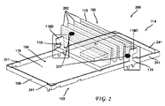
FIG. 1 shows a
電子機器100は、カバー150、側壁151、底フレーム152、発熱部品を載せたプリント回路基板(PCB)101、ヒートシンク取り付け装置(ここでは同義的に“バネ挟み又は曲げタブアセンブリ”とも呼ばれる。)114、並びに熱パッド及び/又は集積回路チップ118であることができる要素118を有する。熱パッドの場合において、熱パッド118は、PCB101の上及び/又はヒートシンク115の底面195の上にあることができる。熱パッド118は、熱除去を促すよう、PCB101に又はヒートシンク115の底面195に取り付けられ得る。集積回路チップの場合において、ヒートシンク115又はヒートシンクの下にある接触パッド(図示せず。)は、PCB101の上のチップ118と接することができる。加えて、両方の場合において、集積回路チップはPCB101の上にあることができ、熱パッドは集積回路チップの上にあることができ、このとき、ヒートシンク115は熱パッドの上に設置される。それら及び他の構成は、本原理の主旨を保ちながら、ここで与えられている本原理の教示を鑑み、当業者によって容易に確定される。
The
PCB101は底面191及び上面192を備える。ヒートシンク115は底面195及び上面196を備える(図4を参照)。
The
図1に示されるように、側壁151はカバー150に垂直である。底フレーム152はカバー150と平行である。電子機器100のフロントパネルは、PCB101を示すために取り外されている。
As shown in FIG. 1, the
ヒートシンク115は、全体的に平坦な水平基部281及び一連の垂直に方向付けられたフィン又は列(以降“フィン”)282を備えることができる。フィン282の夫々は、実質的にPCB101の端から反対の端まで延在することができる。フィン282は、表面積を最大限として放射率を高めるのを助けることができる一連の溝283を備えることができる。特定の実施形態において、ヒートシンク115は、PCB101の上から見た表面積の50%未満をカバーすることができる。他の実施形態において、ヒートシンク115は、PCB101の上から見た表面積の25%未満をカバーすることができる。当然、他のパーセンテージがまた、本原理の主旨を保ちながら、本原理の教示に従って使用可能である。
The
バネ挟み又は曲げタブアセンブリ114は、バネ挟み又は曲げタブ119を含む。バネ挟み又は曲げタブアセンブリ114は、例えば、PCB101及び/又はフレーム152にボルトで固定され、半田付けされ、クリップ留めされ、鋲留めされ及び/又はネジ留めされ得る。ヒートシンク115は、バネ挟み又は曲げタブ119を用いて電子機器100(又はその要素)に取り付けられる。バネ挟み又は曲げタブ119は、個体、又はシールド116の部分であることができる。シールド116は、底面193及び上面194並びにシールド116の外周118にある側壁241を備える。側壁241は、PCB101の外周166に実質的に従うことができる。側壁241は、垂直であり、バネ挟み又は曲げタブ119と一体化され得る。バネ挟み又は曲げタブ119は、ヒートシンク115の平坦な水平基部281の外周176に位置付けられ得る。係合される場合に、バネ挟み又は曲げタブ119は、ヒートシンク115を定位置に保持し、ヒートシンク115がゆるむことを防ぎ、このようにして、ヒートシンク115を固定するための低価格の方法を提供する。
Spring pinch or bending
シールド116においてバネ挟み又は曲げタブ119を含めることによって、費用は下げられ、空間は節約され得る。その理由は、PCB101にあるヒートシンク取り付け穴が、コンパクト且つ高密度の電気設計のトレースレイアウトの利用を悪化させるためである。例えば、PCBにおける3ミリメートル(mm)の取り付け穴の使用を回避することは、単層において穴によって明け渡されるPCB空間において容易に余分の12のトレースをレイアウトされるようにすることができる。多層PCBについて、トレースランの増加はますます大きくなる。
By including a spring clamp or
当然ながら、ここで記載される本原理の様々な実施形態は、ヒートシンクを押さえつけるために使用される、ヒートシンクの上部とカバーとの間のプラスチックバネ仕掛けのピンに対して利点を有する。そのようなピンは、ヒートシンクが冷却しているチップの直ぐ周りの基板上の空間とともに基部に“耳”を備えることをヒートシンクに要求する。チップの周りの穴のための空間は、このような取り付けに必要とされる穴が経路を決められたトレースを横切ることがあり得るために、時々見つけるのが困難であり得る。本原理のそのような及び他の利点は、ここで与えられている本原理の教示を鑑み、当業者に容易に理解される。 Of course, the various embodiments of the present principles described herein have advantages over plastic spring-loaded pins between the top of the heat sink and the cover used to hold down the heat sink. Such pins require the heat sink to have “ears” at the base along with the space on the substrate immediately around the chip the heat sink is cooling. The space for the holes around the tip can sometimes be difficult to find because the holes required for such attachments can cross the routed trace. Such and other advantages of the present principles will be readily apparent to those skilled in the art in view of the teachings of the present principles provided herein.
本原理は、(例えば、無線周波数(RF)放射からの)遮蔽及び吸熱を必要とするシステムに適用可能である。シールドをヒートシンクホルダと併せる考えは、資金及び空間を節約する。バネ挟み又は曲げタブ119のための場所を空けるよう、切断がシールド116において行われてよく、あるいは、バネ挟み又は曲げタブ119は、シールド116とともに単一の一体成形の金属から形成されてよく、あるいは、バネ挟み又は曲げタブ119は、シールド壁241に溶接されるか又は留め具で締められてよい。このように、バネ挟み又は曲げタブ119は、例えば、単一の一体成形の金属から集合的に作られること、一緒に半田付けされること、一緒に溶接されること、一緒に固められること、等によって、実質的に恒久的にシールド116に取り付けられ得る。代替的に、バネ挟み又は曲げタブは、例えば、ネジ、ボルト、クリップ、バネ、等を用いて、着脱可能にシールドに取り付けられ得る。
The present principles are applicable to systems that require shielding and heat absorption (eg, from radio frequency (RF) radiation). The idea of combining a shield with a heat sink holder saves money and space. A cut may be made in the
明示的に示されていないが、当然ながら、例えば、しかし制限なしに、スマートカードソケット、照明部品、受信器部品、ハードドライブ、等のような他の構成要素が電子機器100に存在することができる。
Although not explicitly shown, it will be appreciated that other components may be present in the
図2は、本原理の実施形態に従って、バネ挟み又は曲げタブ119が係合されていない状態でのヒートシンク115及びバネ挟み又は曲げタブアセンブリ114の透視図299を示す。ここで、バネ挟み又は曲げタブ119(明りょうさのために丸で囲まれている。)は係合されていないが、バネ挟み又は曲げタブ119の遠位接触端119Dが内側に向けて捻られるか又は回転される場合に、それらは接触点221でヒートシンク115と接し、ヒートシンク115を押さえつける。当然ながら、接触点221は、ヒートシンク115の溝283の1以上及び/又は上面196のいずれかの部分であることができる。
FIG. 2 shows a
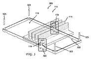
図3は、本原理の実施形態に従って、バネ挟み又は曲げタブ119が係合された状態でのヒートシンク115及びバネ挟み又は曲げタブアセンブリ114の他の透視図399を示す。ヒートシンク115は、バネ挟み又は曲げタブ119(明りょうさのために丸で囲まれている。)が明らかに見えるように、持ち上げられているように示される。ここで、バネ挟み又は曲げタブ119は、ヒートシンク115に接するよう曲がっている(すなわち、捻られるか又は回転されるか又は変形される)ことによって、係合される。特に、バネ挟み又は曲げタブ119の遠位接触端119Dは、ヒートシンク115と接するよう内側に向けて曲がっている。このように、遠位接触端119Dは、ヒートシンク115を定位置に留め、一定量の圧力をヒートシンク115、例えば、その下にあるチップ(又は他の要素)に加え続ける。バネ挟み又は曲げタブ119の遠位接触端119Dは、ヒートシンク115の隣り合うフィンの間に位置付けられ得る。
FIG. 3 illustrates another
シールドタブ322は、シールド壁241から下方向に延在することができ、それらのタブ322は、例えばヒートシンク115の底面195(図4を参照)又はPCB101の底面191又は電子機器100内の内部フレーム等の構成要素に巻き付くよう内側に向けて曲げることができる。シールドタブ322は、シールド116を電子機器100に固定するのを助けることができる。代替的に、及び/又は追加的に、ボルト、ネジ、及び/又は鋲323は、シールド116をPCB101及び/又は電子機器100のフレームに、例えば、シールド116における相補的な穴を通じて、取り付けるために使用され得る。
The
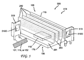
図4は、本原理の実施形態に従って、他のバネ挟み又は曲げタブアセンブリ414の斜視図499を示す。バネ挟み又は曲げタブアセンブリ414は、ペーパークリップ様のバネ挟み又は曲げタブ419を用いることによってヒートシンク115を留め下げる。バネ挟み又は曲げタブ419は、ヒートシンク115と接してそれを定位置に保持するよう、内側に向けて曲げられ且つ下向きに方向付けられ得る。バネ挟み又は曲げタブ419は、シールド116と別個であることができ、シールド116又はPCB101又はフレーム(例えば、底フレーム152)に溶接又は半田付けされ得る。図4において、ヒートシンク115は、PCB101の上面192(図4では図示せず。)に及び/又はヒートシンク115の底面195に設置される熱的接触パッド118の上に設置される。バネ挟み又は曲げタブ419は、シールド116の外に設置され得、ヒートシンク115は、上から嵌め留めされ得る。
FIG. 4 shows a
図5は、本原理の実施形態に従って、他のバネ挟み又は曲げタブアセンブリ514の斜視図599を示し、図6は、本原理の実施形態に従って、他のバネ挟み又は曲げタブアセンブリ614の斜視図699を示す。バネ挟み又は曲げタブ514は、バネ挟み又は曲げタブ519を有する。バネ挟み又は曲げタブアセンブリ614は、バネ挟み又は曲げタブ619を有する。バネ挟み又は曲げタブ519は夫々、ヒートシンク115の接触点221と係合するよう3つの辺から取り付けられ且つヒートシンク115に向かってバネ挟み又は曲げタブ519の上部分から曲がる各々の突起519Dを有する。バネ挟み又は曲げタブ619は夫々、ヒートシンク115の接触点221と係合するよう1つの辺から取り付けられ且つヒートシンク115に向かってバネ挟み又は曲げタブの対応する辺から曲がる各々の突起を有する。バネ挟み又は曲げタブアセンブリ514及び/又はバネ挟み又は曲げタブアセンブリ614は、シールド116と別個であることができ、それらはまた、ヒートシンク115を押さえつけるようシールド116又はPCB101又はフレーム(例えば、底フレーム152)に溶接又は半田付けされ得る。
FIG. 5 shows a
1又はそれ以上の実施形態において、バネ挟み又は曲げタブの部分は、フィン若しくはレール282の間にある上面で及び/又はフィン若しくはレール282の外側の面でヒートシンク115と接することができる。
In one or more embodiments, the portion of the spring clamp or bending tab can contact the
図7は、本原理の実施形態に従って、ヒートシンク取り付け装置を提供する方法700のフローチャートを示す。ステップ705で、一体の金属薄板を設ける。ステップ710で、水平な回路基板の外周を囲むよう金属薄板上に垂直な側壁を形成する。ステップ715で、垂直は側壁から上方向に、又は垂直な側壁に隣接して回路基板から上方向に突き出すタブを設ける。ステップ715は、タブを一体の金属薄板において形成すること、又はタブをシールドに取り付けることを含むことができる。ステップ720で、先に形成された金属薄板を、垂直な側壁が回路基板の外周を囲むように位置付ける。ステップ725で、先に形成された金属薄板を回路基板又は回路基板の下にあるフレーム部品に取り付ける。ステップ730で、回路基板及び回路基板上の部品から熱を取り出すためのヒートシンクを回路基板の上に設置する。ステップ735で、ヒートシンクの上面と接して下方向の力をヒートシンクに加え、ヒートシンクが回路基板及び回路基板上の部品のうちの少なくとも1つと接するように、タブを曲げ、ねじり、回転させ、又は変形させる。
FIG. 7 shows a flowchart of a
本原理のそれら及び多の特徴及び利点は、ここでの教示に基づき当業者によって容易に確かめられ得る。ここでの教示を鑑み、当業者は、本原理のそれら及び同様の実施又は構成を考えることができるであろう。 These and many features and advantages of the present principles can be readily ascertained by one skilled in the art based on the teachings herein. In view of the teachings herein, one of ordinary skill in the related art will be able to contemplate these and similar implementations or configurations of the present principles.
例となる実施形態が添付の図面を参照してここで記載されてきたが、当然ながら、本原理はそれらの厳密な実施形態に制限されず、様々な変更及び改良は、本原理の主旨又は適用範囲から逸脱することなしに、当業者によってそれらにおいて達成され得る。全てのそのような変更及び改良は、添付の特許請求の範囲において記載される本原理の適用範囲内に含まれるよう意図される。 While exemplary embodiments have been described herein with reference to the accompanying drawings, it should be understood that the present principles are not limited to those precise embodiments, and that various changes and modifications may be made to the spirit or principles of the present principles. They can be achieved by those skilled in the art without departing from the scope of application. All such changes and modifications are intended to be included within the scope of the present principles as set forth in the appended claims.
[関連出願の相互参照]
本願は、2012年10月19日付けで出願された米国特許仮出願第61/715876号に基づく優先権を主張するものであり、この米国出願は、その全文を参照により本願に援用される。
[Cross-reference of related applications]
This application claims priority from US Provisional Application No. 61 / 715,766 filed Oct. 19, 2012, which is hereby incorporated by reference in its entirety.
Claims (20)
バネ挟みと、
全体的に平坦な水平基部及び一連の垂直に方向付けられたフィンを備え、前記回路基板の上に配置されて前記回路基板及び該回路基板上の前記部品からの熱が解放又は放散されるヒートシンクと
を有し、
前記ヒートシンクは、前記水平基部の外周に位置付けられる前記バネ挟みによって、前記回路基板及び該回路基板上の少なくとも1つの前記部品のうちの少なくとも1つに固定され、前記バネ挟みは、前記水平基部に接して下方向の力を加える遠位接触端を備える、
電子機器。 A circuit board on which a heat generating component is placed;
With a spring clamp,
A heat sink with a generally flat horizontal base and a series of vertically oriented fins disposed on the circuit board to release or dissipate heat from the circuit board and the components on the circuit board And
The heat sink is fixed to at least one of the circuit board and at least one of the components on the circuit board by the spring clamp positioned on the outer periphery of the horizontal base, and the spring clamp is attached to the horizontal base. A distal contact end that touches and applies a downward force;
Electronics.
請求項1に記載の電子機器。 A shield attached to at least one of the bottom surface of the circuit board and the bottom frame of the electronic device, and the shield is further attached to the spring clamp;
The electronic device according to claim 1.
請求項2に記載の電子機器。 The shield is substantially permanently attached to at least one of the bottom surface of the circuit board and the bottom frame of the electronic device;
The electronic device according to claim 2.
請求項2に記載の電子機器。 The shield is detachably attached to at least one of the bottom surface of the circuit board and the bottom frame of the electronic device.
The electronic device according to claim 2.
請求項2に記載の電子機器。 The shield has a winding-type bending tab for attaching the shield to at least one of the bottom surface of the circuit board and the bottom frame of the electronic device.
The electronic device according to claim 2.
請求項2に記載の電子機器。 The shield includes a side wall that surrounds an outer periphery of the circuit board.
The electronic device according to claim 2.
請求項2に記載の電子機器。 The spring pinch is detachably attached to the shield.
The electronic device according to claim 2.
請求項1に記載の電子機器。 The heat sink has a series of grooves interspersed between the series of fins above the horizontal base and the distal contact end is in a downward direction on one or more of the grooves Apply force,
The electronic device according to claim 1.
請求項1に記載の電子機器。 A shield attached to at least one of the bottom surface of the circuit board and the bottom frame of the electronic device, and the spring clamp is attached to the circuit board and installed outside the outer periphery of the shield;
The electronic device according to claim 1.
前記カバーに垂直な側壁と、
前記カバーと平行な底フレームと、
発熱部品を載せた回路基板と、
曲げタブと、
全体的に平坦な水平基部及び一連の垂直に方向付けられたフィンを備え、前記回路基板の上に配置されて前記回路基板及び該回路基板上の前記部品からの熱が解放又は放散されるヒートシンクと
を有し、
前記ヒートシンクは、前記水平基部上に位置付けられる前記曲げタブによって、前記回路基板及び該回路基板上の少なくとも1つの前記部品のうちの少なくとも1つに固定され、前記曲げタブは、前記水平基部に接して下方向の力を加える遠位接触端を備える、
電子機器。 A cover,
A side wall perpendicular to the cover;
A bottom frame parallel to the cover;
A circuit board on which a heat generating component is placed;
Bending tabs,
A heat sink with a generally flat horizontal base and a series of vertically oriented fins disposed on the circuit board to release or dissipate heat from the circuit board and the components on the circuit board And
The heat sink is secured to at least one of the circuit board and at least one of the components on the circuit board by the bending tab positioned on the horizontal base, the bending tab contacting the horizontal base. A distal contact end for applying a downward force
Electronics.
請求項10に記載の電子機器。 A shield attached to at least one of the bottom surface of the circuit board and the bottom frame of the electronic device, the shield further attached to the bending tab;
The electronic device according to claim 10.
請求項11に記載の電子機器。 The shield is substantially permanently attached to at least one of the bottom surface of the circuit board and the bottom frame of the electronic device;
The electronic device according to claim 11.
請求項11に記載の電子機器。 The shield is detachably attached to at least one of the bottom surface of the circuit board and the bottom frame of the electronic device.
The electronic device according to claim 11.
請求項11に記載の電子機器。 The shield has a winding-type bending tab for attaching the shield to at least one of the bottom surface of the circuit board and the bottom frame of the electronic device.
The electronic device according to claim 11.
請求項11に記載の電子機器。 The bending tab is substantially permanently attached to the shield;
The electronic device according to claim 11.
請求項10に記載の電子機器。 The heat sink has a series of grooves interspersed between the series of fins above the horizontal base and the distal contact end is in a downward direction on one or more of the grooves Apply force,
The electronic device according to claim 10.
請求項10に記載の電子機器。 The shield further includes a shield attached to at least one of the bottom surface of the circuit board and the bottom frame of the electronic device, and the bending tab is attached to the circuit board and installed outside the outer periphery of the shield. ,
The electronic device according to claim 10.
水平な回路基板の外周を囲むよう前記金属薄板上に垂直な側壁を形成するステップと、
前記垂直な側壁から上方向に、又は前記垂直な側壁に隣接して前記回路基板から上方向に突き出すタブを設けるステップと、
前記垂直な側壁が前記回路基板の外周を囲むように前記形成された金属薄板を位置付けるステップと、
前記形成された金属薄板を前記回路基板又は該回路基板の下にあるフレーム部品に取り付けるステップと、
前記回路基板及び該回路基板上の部品から熱を取り出すためのヒートシンクを前記回路基板の上に設置するステップと、
前記ヒートシンクの上面と接して下方向の力を前記ヒートシンクに加え、該ヒートシンクが前記回路基板及び該回路基板上の前記部品のうちの少なくとも1つと接するように、前記タブを曲げ、ねじり、回転させ、又は変形させるステップと
を有する方法。 Providing an integral sheet metal;
Forming a vertical side wall on the metal thin plate so as to surround an outer periphery of a horizontal circuit board;
Providing a tab projecting upward from the vertical side wall or adjacent to the vertical side wall from the circuit board; and
Positioning the formed sheet metal so that the vertical sidewall surrounds the outer periphery of the circuit board;
Attaching the formed metal sheet to the circuit board or a frame component under the circuit board;
Installing a heat sink on the circuit board for extracting heat from the circuit board and components on the circuit board;
A downward force is applied to the heat sink in contact with the top surface of the heat sink, and the tab is bent, twisted, and rotated so that the heat sink contacts at least one of the circuit board and the component on the circuit board. Or a step of deforming.
請求項18に記載の方法。 Providing the tab protruding upward from the vertical sidewall includes forming the tab on the unitary sheet metal;
The method of claim 18.
請求項18に記載の方法。
The step of providing a tab projecting upwardly from the side wall vertically includes attaching the tab to a shield;
The method of claim 18.
Applications Claiming Priority (3)
| Application Number | Priority Date | Filing Date | Title |
|---|---|---|---|
| US201261715876P | 2012-10-19 | 2012-10-19 | |
| US61/715,876 | 2012-10-19 | ||
| PCT/US2013/065529 WO2014062974A1 (en) | 2012-10-19 | 2013-10-17 | Heat sink attachment apparatus and method |
Publications (2)
| Publication Number | Publication Date |
|---|---|
| JP2015537377A true JP2015537377A (en) | 2015-12-24 |
| JP2015537377A5 JP2015537377A5 (en) | 2016-12-01 |
Family
ID=49519112
Family Applications (1)
| Application Number | Title | Priority Date | Filing Date |
|---|---|---|---|
| JP2015537844A Withdrawn JP2015537377A (en) | 2012-10-19 | 2013-10-17 | Heat sink mounting apparatus and method |
Country Status (7)
| Country | Link |
|---|---|
| US (1) | US9603286B2 (en) |
| EP (1) | EP2910095B1 (en) |
| JP (1) | JP2015537377A (en) |
| KR (1) | KR20150073992A (en) |
| CN (1) | CN105009699A (en) |
| BR (1) | BR112015008465B1 (en) |
| WO (1) | WO2014062974A1 (en) |
Families Citing this family (12)
| Publication number | Priority date | Publication date | Assignee | Title |
|---|---|---|---|---|
| US20170273169A1 (en) * | 2014-09-24 | 2017-09-21 | Hewlett Packard Enterprise Development Lp | Heat sink with a load spreading bar |
| US10356948B2 (en) | 2015-12-31 | 2019-07-16 | DISH Technologies L.L.C. | Self-adjustable heat spreader system for set-top box assemblies |
| US10624245B2 (en) * | 2016-06-23 | 2020-04-14 | Laird Technologies, Inc. | Laser weldable brackets for attachment of heat sinks to board level shields |
| US9893474B1 (en) * | 2016-10-12 | 2018-02-13 | International Business Machines Corporation | Active cable heat sink |
| CN106507651B (en) * | 2016-12-30 | 2019-11-29 | 韩端科技(深圳)有限公司 | Electronic equipment |
| US10785864B2 (en) * | 2017-09-21 | 2020-09-22 | Amazon Technologies, Inc. | Printed circuit board with heat sink |
| USD835590S1 (en) | 2018-06-27 | 2018-12-11 | Advanced Thermal Solutions, Inc. | Heat sink clip |
| USD876372S1 (en) | 2018-06-27 | 2020-02-25 | Advanced Thermal Solutions, Inc. | Heat sink clip and attachment |
| USD837753S1 (en) | 2018-06-27 | 2019-01-08 | Advanced Thermal Solutions, Inc. | Heat sink clip |
| USD877098S1 (en) | 2018-06-27 | 2020-03-03 | Advanced Thermal Solutions, Inc. | Heat sink clip and attachment |
| EP3908901A1 (en) * | 2019-01-10 | 2021-11-17 | Makersan Makina Otomotiv Sanayi Ticaret Anonim Sirketi | Joystick with a precise control |
| US11778728B2 (en) * | 2020-10-28 | 2023-10-03 | Arris Enterprises Llc | Pass-through latching heat sink |
Family Cites Families (25)
| Publication number | Priority date | Publication date | Assignee | Title |
|---|---|---|---|---|
| US5304735A (en) * | 1992-02-14 | 1994-04-19 | Aavid Engineering, Inc. | Heat sink for an electronic pin grid array |
| US5436798A (en) * | 1994-01-21 | 1995-07-25 | Wakefield Engineering, Inc. | Spring clip and heat sink assembly for electronic components |
| US5411199A (en) * | 1994-03-07 | 1995-05-02 | Motorola, Inc. | Method for attaching a shield |
| SE9401203L (en) * | 1994-04-11 | 1995-10-12 | Ellemtel Utvecklings Ab | Screen and cooler |
| US5621244A (en) * | 1994-05-16 | 1997-04-15 | Lin; Shih-Jen | Fin assembly for an integrated circuit |
| GB2295927A (en) * | 1994-12-08 | 1996-06-12 | Gareth Rhys Baron | Mounting of an integrated circuit on a printed circuit board |
| US5570271A (en) * | 1995-03-03 | 1996-10-29 | Aavid Engineering, Inc. | Heat sink assemblies |
| US5576933A (en) | 1995-05-15 | 1996-11-19 | Wakefield Engineering, Inc. | Clamping heat sink for an electric device |
| US5881800A (en) * | 1998-04-03 | 1999-03-16 | Chung; Kuang-Hua | Heat sink fastener |
| CN2342343Y (en) * | 1998-08-04 | 1999-10-06 | 钟光华 | Fixing base structure for radiator |
| US6617685B1 (en) * | 1999-08-30 | 2003-09-09 | Sun Microsystems, Inc. | Clip heat sink assembly |
| EP1128432B1 (en) * | 2000-02-24 | 2016-04-06 | Infineon Technologies AG | Fixation of semiconductor modules to a heatsink |
| US7061774B2 (en) | 2000-12-18 | 2006-06-13 | Franklin Zhigang Zhang | Computer board with dual shield housing and heat sink expansion zone apparatuses |
| US6856511B1 (en) * | 2003-07-17 | 2005-02-15 | Cisco Technology, Inc. | Methods and apparatus for attaching a heat sink to a circuit board component |
| US8902603B2 (en) | 2004-02-06 | 2014-12-02 | Carmen Rapisarda | Solder and lead free electronic circuit and method of manufacturing same |
| JP2006222388A (en) * | 2005-02-14 | 2006-08-24 | Toshiba Corp | Heat dissipation device and heat dissipation method of electronic apparatus |
| CN1953646A (en) * | 2005-10-18 | 2007-04-25 | 鸿富锦精密工业(深圳)有限公司 | Heat radiator capable of preventing electromagnetic interference |
| US7355857B2 (en) * | 2006-02-07 | 2008-04-08 | Methode Electronics, Inc. | Heat sink gasket |
| US7804696B2 (en) * | 2006-12-07 | 2010-09-28 | Finisar Corporation | Electromagnetic radiation containment in an electronic module |
| JPWO2008099554A1 (en) * | 2007-02-15 | 2010-05-27 | 日本電気株式会社 | Semiconductor package mounting structure |
| US7567439B2 (en) | 2007-08-10 | 2009-07-28 | Fu Zhun Precision Industry (Shen Zhen) Co., Ltd. | Heat dissipation device having a rotatable fastener |
| CN101754639A (en) * | 2008-12-02 | 2010-06-23 | 台达电子工业股份有限公司 | Fixing structure of radiator |
| CN201726632U (en) * | 2010-04-15 | 2011-01-26 | 鸿富锦精密工业(深圳)有限公司 | Cooling plate fixing structure of electronic products |
| US20140036451A1 (en) * | 2012-07-31 | 2014-02-06 | Glenn C. Simon | Heat sink assembly |
| US9146062B2 (en) * | 2013-03-01 | 2015-09-29 | Radian Thermal Products, Inc. | Interlocking clip heatsink mounting system |
-
2013
- 2013-10-17 JP JP2015537844A patent/JP2015537377A/en not_active Withdrawn
- 2013-10-17 BR BR112015008465-6A patent/BR112015008465B1/en active IP Right Grant
- 2013-10-17 EP EP13786360.1A patent/EP2910095B1/en active Active
- 2013-10-17 WO PCT/US2013/065529 patent/WO2014062974A1/en active Application Filing
- 2013-10-17 CN CN201380054313.9A patent/CN105009699A/en active Pending
- 2013-10-17 KR KR1020157010075A patent/KR20150073992A/en not_active Application Discontinuation
- 2013-10-17 US US14/435,049 patent/US9603286B2/en active Active
Also Published As
| Publication number | Publication date |
|---|---|
| EP2910095A1 (en) | 2015-08-26 |
| BR112015008465B1 (en) | 2021-07-20 |
| US9603286B2 (en) | 2017-03-21 |
| BR112015008465A2 (en) | 2017-07-04 |
| KR20150073992A (en) | 2015-07-01 |
| WO2014062974A1 (en) | 2014-04-24 |
| CN105009699A (en) | 2015-10-28 |
| EP2910095B1 (en) | 2019-08-14 |
| US20150282388A1 (en) | 2015-10-01 |
Similar Documents
| Publication | Publication Date | Title |
|---|---|---|
| JP2015537377A (en) | Heat sink mounting apparatus and method | |
| US7333338B2 (en) | Memory module assembly including a clip for mounting a heat sink thereon | |
| US7468890B2 (en) | Graphics card heat-dissipating device | |
| US7660114B2 (en) | Heat dissipating member, heat dissipating mechanism, and information processing apparatus | |
| JP2011066399A (en) | Heat dissipation device | |
| US10568206B2 (en) | Printed circuit board assembly and assembling method thereof | |
| TW201314425A (en) | Radiator device and electronic device using same | |
| JP2011155056A (en) | Shielding structure | |
| US20090310302A1 (en) | Heat-dissipating structure having an external fan | |
| US20140247564A1 (en) | Shielding structure for electronic device | |
| JP5686127B2 (en) | Signal transmission device | |
| US20150305137A1 (en) | Electronic device with combination heat sink/blower or fan assembly having air duct | |
| CN111713184A (en) | Heat sink assembly for electronic device | |
| JP5738679B2 (en) | Heat dissipation structure | |
| JP2014239105A (en) | Mounting structure between power supply circuit board and chassis | |
| US7881061B2 (en) | Mounting device for mounting heat sink onto electronic component | |
| JP2017108007A (en) | Heat radiation structure for heat evolution electronic component and manufacturing method for the same | |
| JP5717619B2 (en) | Electronic equipment unit | |
| US9596783B2 (en) | Electronic device with combination heat sink/blower or fan assembly | |
| JP2010251637A (en) | Heat radiation mechanism and information equipment | |
| JP3143705U (en) | Heat sink backboard in integrated circuit | |
| CN117898031A (en) | Apparatus for providing thermal management and electromagnetic interference shielding | |
| TW201506586A (en) | Server | |
| KR20100054356A (en) | Heat sink and display apparatus having the same | |
| KR20000012643U (en) | Heat sink for combining heating electronic parts of TV |
Legal Events
| Date | Code | Title | Description |
|---|---|---|---|
| A521 | Request for written amendment filed |
Free format text: JAPANESE INTERMEDIATE CODE: A523 Effective date: 20161012 |
|
| A621 | Written request for application examination |
Free format text: JAPANESE INTERMEDIATE CODE: A621 Effective date: 20161012 |
|
| A761 | Written withdrawal of application |
Free format text: JAPANESE INTERMEDIATE CODE: A761 Effective date: 20170324 |