JP2015507231A - Capacitive touch device pattern and manufacturing method thereof - Google Patents
Capacitive touch device pattern and manufacturing method thereof Download PDFInfo
- Publication number
- JP2015507231A JP2015507231A JP2014533758A JP2014533758A JP2015507231A JP 2015507231 A JP2015507231 A JP 2015507231A JP 2014533758 A JP2014533758 A JP 2014533758A JP 2014533758 A JP2014533758 A JP 2014533758A JP 2015507231 A JP2015507231 A JP 2015507231A
- Authority
- JP
- Japan
- Prior art keywords
- axis
- conductive wiring
- adjacent
- wiring
- touch device
- Prior art date
- Legal status (The legal status is an assumption and is not a legal conclusion. Google has not performed a legal analysis and makes no representation as to the accuracy of the status listed.)
- Pending
Links
Images


Classifications
-
- G—PHYSICS
- G06—COMPUTING; CALCULATING OR COUNTING
- G06F—ELECTRIC DIGITAL DATA PROCESSING
- G06F3/00—Input arrangements for transferring data to be processed into a form capable of being handled by the computer; Output arrangements for transferring data from processing unit to output unit, e.g. interface arrangements
- G06F3/01—Input arrangements or combined input and output arrangements for interaction between user and computer
- G06F3/03—Arrangements for converting the position or the displacement of a member into a coded form
- G06F3/041—Digitisers, e.g. for touch screens or touch pads, characterised by the transducing means
- G06F3/044—Digitisers, e.g. for touch screens or touch pads, characterised by the transducing means by capacitive means
- G06F3/0443—Digitisers, e.g. for touch screens or touch pads, characterised by the transducing means by capacitive means using a single layer of sensing electrodes
-
- G—PHYSICS
- G06—COMPUTING; CALCULATING OR COUNTING
- G06F—ELECTRIC DIGITAL DATA PROCESSING
- G06F3/00—Input arrangements for transferring data to be processed into a form capable of being handled by the computer; Output arrangements for transferring data from processing unit to output unit, e.g. interface arrangements
- G06F3/01—Input arrangements or combined input and output arrangements for interaction between user and computer
- G06F3/03—Arrangements for converting the position or the displacement of a member into a coded form
- G06F3/041—Digitisers, e.g. for touch screens or touch pads, characterised by the transducing means
- G06F3/044—Digitisers, e.g. for touch screens or touch pads, characterised by the transducing means by capacitive means
- G06F3/0446—Digitisers, e.g. for touch screens or touch pads, characterised by the transducing means by capacitive means using a grid-like structure of electrodes in at least two directions, e.g. using row and column electrodes
-
- G—PHYSICS
- G06—COMPUTING; CALCULATING OR COUNTING
- G06F—ELECTRIC DIGITAL DATA PROCESSING
- G06F2203/00—Indexing scheme relating to G06F3/00 - G06F3/048
- G06F2203/041—Indexing scheme relating to G06F3/041 - G06F3/045
- G06F2203/04103—Manufacturing, i.e. details related to manufacturing processes specially suited for touch sensitive devices
-
- G—PHYSICS
- G06—COMPUTING; CALCULATING OR COUNTING
- G06F—ELECTRIC DIGITAL DATA PROCESSING
- G06F2203/00—Indexing scheme relating to G06F3/00 - G06F3/048
- G06F2203/041—Indexing scheme relating to G06F3/041 - G06F3/045
- G06F2203/04111—Cross over in capacitive digitiser, i.e. details of structures for connecting electrodes of the sensing pattern where the connections cross each other, e.g. bridge structures comprising an insulating layer, or vias through substrate
-
- Y—GENERAL TAGGING OF NEW TECHNOLOGICAL DEVELOPMENTS; GENERAL TAGGING OF CROSS-SECTIONAL TECHNOLOGIES SPANNING OVER SEVERAL SECTIONS OF THE IPC; TECHNICAL SUBJECTS COVERED BY FORMER USPC CROSS-REFERENCE ART COLLECTIONS [XRACs] AND DIGESTS
- Y10—TECHNICAL SUBJECTS COVERED BY FORMER USPC
- Y10T—TECHNICAL SUBJECTS COVERED BY FORMER US CLASSIFICATION
- Y10T29/00—Metal working
- Y10T29/49—Method of mechanical manufacture
- Y10T29/49002—Electrical device making
- Y10T29/49105—Switch making
Landscapes
- Engineering & Computer Science (AREA)
- General Engineering & Computer Science (AREA)
- Theoretical Computer Science (AREA)
- Human Computer Interaction (AREA)
- Physics & Mathematics (AREA)
- General Physics & Mathematics (AREA)
- Position Input By Displaying (AREA)
- Manufacture Of Switches (AREA)
Abstract
本発明はタッチデバイスに係り、特に容量タッチデバイスのパターンとその製造方法に関する。この容量タッチデバイスのパターンは、基板、2つの互いに隣接した第1軸の電極、第1軸の導電配線、および一対の金属ジャンパを備える。第1軸の導電配線は、2つの互いに隣接した第1軸の電極を接続するために、2つの互いに隣接した第1軸の電極の間に設けられる。一対の金属ジャンパは、2つの第1軸の電極と第1軸の導電配線との接続部上に設けられる。これによって、2つの互いに隣接した第1軸の電極と第1軸の導電配線との接続部によって引き起こされる抵抗を低減することができ、容量タッチ制御デバイスのパターンの応答速度を増大することができる。The present invention relates to a touch device, and more particularly to a pattern of a capacitive touch device and a manufacturing method thereof. The pattern of the capacitive touch device includes a substrate, two mutually adjacent first axis electrodes, a first axis conductive wiring, and a pair of metal jumpers. The first-axis conductive wiring is provided between two adjacent first-axis electrodes to connect two adjacent first-axis electrodes. The pair of metal jumpers is provided on a connection portion between the two first-axis electrodes and the first-axis conductive wiring. As a result, the resistance caused by the connection between two adjacent first axis electrodes and the first axis conductive wiring can be reduced, and the response speed of the capacitive touch control device pattern can be increased. .
Description
本発明はタッチデバイスに係り、特に容量タッチデバイスのパターンとその製造方法に関する。 The present invention relates to a touch device, and more particularly to a pattern of a capacitive touch device and a manufacturing method thereof.
電子材料の急速な発展に伴って、タッチデバイスはすでに汎用の入力インターフェイスとなっている。圧力操作または手動操作による従来の入力インターフェイスはまた、近い将来、タッチデバイスに置き換わるであろう。最近では、液晶パネルの活発な開発によって、表示スクリーンが一体化されたタッチデバイスがすでに大量に生産され、売られている。タッチデバイスは、抵抗タッチデバイスと容量タッチデバイスとに分けることができる。既存の家電製品は容量タッチデバイスを大いに利用し、容量デバイスを表示スクリーンに一体化している。 With the rapid development of electronic materials, touch devices have already become general-purpose input interfaces. Traditional input interfaces with pressure or manual operation will also replace touch devices in the near future. Recently, due to the active development of liquid crystal panels, touch devices with integrated display screens have already been produced and sold in large quantities. Touch devices can be divided into resistive touch devices and capacitive touch devices. Existing home appliances make extensive use of capacitive touch devices and integrate capacitive devices into the display screen.
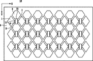
一体化された表示スクリーンにおいて、容量タッチデバイスは通常、平面の2つの軸方向(X軸とY軸)の座標感知力を有する。図1は、従来の容量タッチデバイスのパターンを示す。容量タッチデバイスのパターン10は、基板5を含む。2つの互いに隣接した第1軸の電極1と第1軸の導電配線11とが複数群あり、これらはX軸方向のセンサ電極単位を構成し、タッチ位置のX軸座標の感知に使用される。2つの互いに隣接した第2軸の電極2と第2軸の導電配線21とが複数群あり、これらはY軸方向のセンサ電極単位を構成し、タッチ位置のY軸座標の感知に使用される。第1軸の導電配線11と第2軸の導電配線21とを互いから電気的に絶縁するために、絶縁層4が使われる。上述のセンサ電極単位は、インジウム錫酸化物のような透明導電材料によって形成できる。絶縁層4は通常、ポリイミドのような透明絶縁材料によって形成される。
In an integrated display screen, a capacitive touch device typically has coordinate sensing power in two planar directions (X-axis and Y-axis). FIG. 1 shows a pattern of a conventional capacitive touch device. The capacitive
容量タッチデバイスの応答速度は、X軸方向とY軸方向のセンサ電極単位の抵抗によって制限される。センサ電極単位の抵抗は、主に透明な第1軸の導電配線11によって作られた首部の影響を受ける。従来の容量タッチデバイスのパターンに制限されて、第1軸の導電配線11の面積は通常はより小さく、同時により大きな抵抗を有している。したがって、首部における抵抗を低減し、容量タッチデバイスの応答速度を改善することが課題となっている。
The response speed of the capacitive touch device is limited by the resistance of the sensor electrode unit in the X-axis direction and the Y-axis direction. The resistance of the sensor electrode unit is influenced mainly by the neck portion formed by the transparent first-axis
本発明の目的は、2つの互いに隣接した第1軸の電極と第1軸の導電配線との接続部を横切る金属ジャンパを設けることによって、タッチデバイスの抵抗を効果的に低減し、タッチデバイスの応答速度を増大することが可能な容量タッチデバイスのパターンを提供することである。 It is an object of the present invention to effectively reduce the resistance of a touch device by providing a metal jumper across a connection portion between two adjacent first-axis electrodes and a first-axis conductive wiring. It is to provide a capacitive touch device pattern that can increase the response speed.
一実施形態において、容量タッチデバイスのパターンは、
2つの互いに隣接した第1軸の電極と、
前記2つの互いに隣接した第1軸の電極の間にこれらを接続するために設けられた第1軸の導電配線と、
前記2つの互いに隣接した第1軸の電極と前記第1軸の導電配線との接続部に電気的に接続された一対の金属ジャンパとを備える。
In one embodiment, the capacitive touch device pattern is:
Two adjacent first axis electrodes;
A first-axis conductive wiring provided to connect the two adjacent first-axis electrodes to each other;
A pair of metal jumpers electrically connected to a connection portion between the two adjacent first-axis electrodes and the first-axis conductive wiring;
本発明の他の目的は、以下の工程を有する容量タッチデバイスのパターンの製造方法を提供することである。基板の表面に、2つの互いに隣接した第1軸の電極、第1軸の導電配線、および2つの互いに隣接した第2軸の電極を形成する。ここで、前記第1軸の導電配線は、前記2つの互いに隣接した第1軸の電極の間にこれらを接続するために設けられ、前記2つの互いに隣接した第2軸の電極は、前記第1軸の導電配線の両側に分かれて設けられる。さらに、前記第1軸の導電配線を部分的に覆う絶縁層を形成する。次に、一対の金属ジャンパおよび第2軸の導電配線を形成する。ここで、前記一対の金属ジャンパは、前記2つの互いに隣接した第1軸の電極と前記第1軸の導電配線との接続部上に設けられる。さらに、前記第2軸の導電配線は、前記絶縁層を横切って設けられ、前記2つの互いに隣接した第2軸の電極を接続し、前記第1軸の導電配線と前記第2軸の導電配線とが電気的に絶縁される。 Another object of the present invention is to provide a method for manufacturing a pattern of a capacitive touch device having the following steps. Two adjacent first-axis electrodes, first-axis conductive wiring, and two adjacent second-axis electrodes are formed on the surface of the substrate. Here, the first-axis conductive wiring is provided to connect the two adjacent first-axis electrodes, and the two adjacent second-axis electrodes are connected to the first-axis electrodes. It is provided separately on both sides of the uniaxial conductive wiring. Further, an insulating layer partially covering the first axis conductive wiring is formed. Next, a pair of metal jumpers and a second-axis conductive wiring are formed. Here, the pair of metal jumpers are provided on a connection portion between the two adjacent first-axis electrodes and the first-axis conductive wiring. Further, the second axis conductive wiring is provided across the insulating layer, connects the two adjacent second axis electrodes, and the first axis conductive wiring and the second axis conductive wiring. And are electrically insulated.
本発明の他の目的は、以下の工程を有する容量タッチデバイスのパターンの製造方法を提供することである。基板上に一対の金属ジャンパおよび第2軸の導電配線を形成する。ここで、前記一対の金属ジャンパは、前記第2軸の導電配線の両側に分かれて設けられる。さらに、前記第2軸の導電配線を絶縁層で覆う。次に、前記基板上に、2つの互いに隣接した第1軸の電極、第1軸の導電配線、および2つの互いに隣接した第2軸の電極を形成する。ここで、前記2つの互いに隣接した第2軸の電極は、前記第2軸の導電配線の両端部に分かれて接続される。前記2つの互いに隣接した第1軸の電極は、前記第2軸の導電配線の両側に分かれて設けられる。ここで、前記第1軸の導電配線は前記絶縁層で部分的に覆われ、前記一対のジャンパもまた部分的に覆われる。前記第1軸の導電配線は2つの互いに隣接した第1軸の電極に接続される。前記第1軸の導電配線と前記第2軸の導電配線との間に絶縁層を形成することで、電気的な絶縁が得られる。 Another object of the present invention is to provide a method for manufacturing a pattern of a capacitive touch device having the following steps. A pair of metal jumpers and a second axis conductive wiring are formed on the substrate. Here, the pair of metal jumpers are provided separately on both sides of the second-axis conductive wiring. Furthermore, the conductive wiring of the second axis is covered with an insulating layer. Next, two mutually adjacent first axis electrodes, first axis conductive wirings, and two adjacent second axis electrodes are formed on the substrate. Here, the two adjacent second-axis electrodes are connected separately at both ends of the second-axis conductive wiring. The two adjacent first-axis electrodes are separately provided on both sides of the second-axis conductive wiring. Here, the conductive wiring of the first axis is partially covered with the insulating layer, and the pair of jumpers are also partially covered. The first-axis conductive wiring is connected to two adjacent first-axis electrodes. Electrical insulation can be obtained by forming an insulating layer between the first-axis conductive wiring and the second-axis conductive wiring.
上記から要約するように、本発明における容量タッチデバイスのパターンは、2つの互いに隣接した第1軸の電極と第1軸の導電配線との接続によって引き起こされる抵抗を効果的に低減することができ、これによって、容量タッチデバイスの応答速度を増大することができる。製造方法において、一対の金属ジャンパおよび第2軸の導電配線を完成するのにエッチングが必要であり、これによって追加の製造コストを低減することができる。 As summarized above, the capacitive touch device pattern of the present invention can effectively reduce the resistance caused by the connection between two mutually adjacent first axis electrodes and first axis conductive wiring. Thereby, the response speed of the capacitive touch device can be increased. In the manufacturing method, etching is required to complete the pair of metal jumpers and the second-axis conductive wiring, which can reduce additional manufacturing costs.
当業者にとって、以下に記す実施形態と図面は説明目的だけのためで、いかなる方法によっても本発明の範囲は制限されない。 For those skilled in the art, the embodiments and drawings described below are for illustrative purposes only, and the scope of the present invention is not limited in any way.
図2は、タッチデバイスのパターンの製造方法のフローチャートを示す。図3、4、5は、図2の製造方法の各工程によって製造されるパターンの平面図である。タッチデバイスのパターンの製造方法は、イエローライトプロセスあるいは回路印刷技術を用いることができる。本発明におけるタッチデバイスのパターンの製造方法は以下の工程を含む。 FIG. 2 shows a flowchart of a method of manufacturing a touch device pattern. 3, 4, and 5 are plan views of a pattern manufactured by each process of the manufacturing method of FIG. 2. The touch device pattern manufacturing method can use a yellow light process or a circuit printing technique. The method for manufacturing a touch device pattern according to the present invention includes the following steps.
ステップS11:基板5の表面に、2つの互いに隣接した第1軸の電極1、第1軸の導電配線11、および2つの互いに隣接した第2軸の電極2を形成する。図3に示すように、第1軸の導電配線11は、2つの互いに隣接した第1軸の電極1の間にこれらを互いに接続するために設けられる。2つの互いに隣接した第2軸の電極2は、第1軸の導電配線11の両側に分かれて設けられる。2つの互いに隣接した第1軸の電極1、第1軸の導電配線11、および2つの互いに隣接した第2軸の電極2は、透明導電材料により形成することができる。透明導電材料は、可視光透明性と導電性とを有する。透明導電材料としてはインジウム錫酸化物が挙げられるが、他の種類の透明導電材料もまた、発明の限定を避けるためここではリストしないが、使用できる。第1軸の電極1と第1軸の導電配線11とは、一体成形の構造であってもよい。
Step S <b> 11: Two adjacent first-
ステップS12:図4に示すように、絶縁層4によって第1軸の導電配線11を覆う。絶縁層4はポリイミドのような透明絶縁材料によって形成することができるが、透明絶縁材料の種類は発明の限定を避けるためここではリストしない。
Step S12: As shown in FIG. 4, the
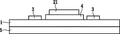
ステップS13:図5に示すように、一対の金属ジャンパ3および第2軸の導電配線21を形成する。この一対の金属ジャンパ3は、2つの互いに隣接した第1軸の電極1と第1軸の導電配線11との接続部上に設けられる。第1軸の導電配線11と第2軸の導電配線21との間で電気的な絶縁を形成するようにして、絶縁層4を横切って設けられた第2軸の導電配線21は、2つの互いに隣接した第2軸の電極2に接続される。図5中のタッチデバイスのパターン40は、ステップS11−S13を通して形成することができる。
Step S13: As shown in FIG. 5, a pair of
図5中の容量タッチデバイスのパターン40において、第1軸の導電配線11は狭くかつ長く、透明導電材料により形成されており、2つの互いに隣接した第1軸の電極1の間の抵抗を比較的高くする。しかしながら、一対の金属ジャンパ3が2つの互いに隣接した第1軸の電極1と第1軸の導電配線11との間の接続部上に設けられた後、2つの互いに隣接した第1軸の電極1の間の抵抗を低減することができ、一体タッチデバイスの感知速度を増大することができる。
In the capacitive
容量タッチデバイスのパターン40は、タッチデバイスのパターン40の完成の後、周辺配線を介して、好ましい導電率で外部の制御部にさらに接続することができる(図1−図4においては示されない)。たとえば、第1軸の周辺配線(図1−図4おいては示されない)と第2軸の周辺配線(図2−図5おいては示されない)とは、第1軸の周辺配線を第1軸の電極1に接続し、第2軸の周辺配線を第2軸の電極2に接続するように、基板5の両側部に形成される。
The capacitive
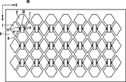
図6は、本実施形態における容量タッチデバイスのパターンの平面図である。タッチデバイスのパターン50は、図5中のタッチデバイスのパターン40をアレイ状に配列することによって、形成される。タッチデバイスのパターン40は、以下の実施形態で述べるタッチデバイスのパターンの方法を使用して、完成することができる。
FIG. 6 is a plan view of the pattern of the capacitive touch device in the present embodiment. The touch device pattern 50 is formed by arranging the
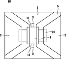
図7Aは、タッチデバイスのパターン40のA軸断面図である。図7Bは、タッチデバイスのパターン40のB軸断面図である。
一実施形態において、タッチデバイスのパターン40は、基板5、2つの互いに隣接した第1軸の電極1、第1軸の導電配線11、2つの互いに隣接した第2軸の電極2、第2軸の導電配線21、絶縁層4、および一対の金属ジャンパ3を含む。2つの互いに隣接した第1軸の電極1、第1軸の導電配線11、および2つの互いに隣接した第2軸の電極2は、基板5の表面に設けられる。第1軸の導電配線11は、2つの互いに隣接した第1軸の電極1の間にこれらを接続するように形成される。2つの互いに隣接した第2軸の電極2は、第1軸の導電配線11の両側に分かれて設けられる。第2軸の導電配線21は、第1軸の導電配線11を横切って延び、2つの互いに隣接した第2軸の電極2に接続されている。絶縁層4は、透明な第1軸の導電配線11と第2軸の導電配線21との間にこれらを電気的に絶縁するように形成される。一対の金属ジャンパ3は、2つの互いに隣接した第1軸の電極1と第1軸の導電配線11との間の接続部上に設けられる。
FIG. 7A is an A-axis cross-sectional view of the
In one embodiment, the
図5および図6において、2つの互いに隣接した第1軸の電極1と第1軸の導電配線11とが複数群あり、これらはX軸方向のセンサ電極単位を構成する。これらのセンサ電極単位は、タッチ位置のX軸座標の感知に使用される。2つの互いに隣接した第2軸の電極2と第2軸の導電配線21とが複数群あり、これらはY軸方向のセンサ電極単位を構成し、タッチ位置のY軸座標の感知に使用される。2つの互いに隣接した透明な第2軸の電極は、ITOのような透明導電材料からなる。第2軸の導電配線21は、モリブデン/アルミニウム/モリブデン、または導電率の良い他の任意の金属からなる金属膜であり得る。このモリブデン/アルミニウム/モリブデン金属膜は、第2軸の導電配線21を完成するためのエッチングプロセスに好適に使用される。
5 and 6, there are a plurality of groups of two first-
絶縁層4は、透明な第1軸の導電配線11と第2軸の導電配線21との間に形成される。第1軸の導電配線11と第2軸の導電配線21との間に適切な電気的な絶縁が形成されるように、第2軸の導電配線21の幅に基づいて適当な面積の絶縁層を選択することができる。絶縁層4は、ポリイミドまたは他の任意の同様の/公知の材料により形成することができる。
The insulating
透明な第1軸の電極1と透明な第1軸の導電配線11とで構成されるX軸方向の電極単位の抵抗を減らすために、一対の金属ジャンパ3が使われる。この一対の金属ジャンパ3は、2つの互いに隣接した第1軸の電極1と第1軸の導電配線11との接続部の近傍に設けることができる。第1軸の導電配線11は第1軸の電極1のそれと比較して相対的に小さな横断面を持つ。このことは、2つの互いに隣接した第1軸の電極1と第1軸の導電配線11とを含む首部の抵抗をより大きくする。このことは、第1軸の電極1と透明な第1軸の導電配線11とで構成されるX軸方向の電極単位の抵抗を増大させる。
A pair of
第1軸の電極1と透明な第1軸の導電配線11とで構成されるX軸方向の電極単位の抵抗は、一対の金属導電配線3によって低減することができる。この抵抗の低減は、タッチデバイスの応答時間を短くすることができ、これによってタッチデバイスの応答速度を増大することができる。ここで、X軸の電極単位の抵抗を計算する方法について述べる。第1軸の電極1の数をNとしたとき、N−1は第1軸の導電配線11の数を表す。X軸方向の電極単位の抵抗は、第1軸の電極1と第1軸の導電配線11との連続的な障害から得られる抵抗に対応する。
言い換えれば、X軸方向の電極単位の抵抗は、第1軸の電極1の抵抗を第1軸の電極1の数だけ掛け、次に2つの互いに隣接した第1軸の電極1と第1軸の導電配線11とで構成される首部の抵抗を加え、最後に首部の数を掛けたものである。
The resistance of the electrode unit in the X-axis direction constituted by the
In other words, the resistance of the electrode unit in the X-axis direction is obtained by multiplying the resistance of the first-
たとえば、個々の第1軸の電極1の抵抗が100Ωであり、個々の首部の抵抗が200Ωであるとする。Nが11であるとき、X軸方向の電極単位の抵抗は、3100Ω(11×100+10×200=3100Ω)である。一対の金属導電配線3を加えると、首部の抵抗は10Ωになる。このとき、X軸方向の電極単位の抵抗は、1200Ω(11×100+10×10=1200Ω)である。
For example, it is assumed that the resistance of each
一対の金属ジャンパ3は任意の金属配線からなり、特に好ましくは、モリブデン、アルミニウム、またはモリブデンを含む金属膜である。エッチングプロセスにより、一対の金属ジャンパ3および第2軸の導電配線21を完成することができる。
The pair of
図8は、タッチデバイスのパターンの製造方法のフローチャートを示す。図9−図11は、タッチデバイスのパターンの製造方法の種々の工程に応じた構造の模式図を示す。タッチデバイスのパターンの製造方法は、イエローライトプロセスあるいは回路印刷技術を用いることができる。図11に示すように、タッチデバイスのパターンの製造方法において製造されるタッチデバイスのパターン90は、タッチデバイスのパターン40の逆重ね構造を有する。タッチデバイスのパターンの製造方法は以下の工程を含む。
FIG. 8 shows a flowchart of a method of manufacturing a touch device pattern. 9 to 11 are schematic diagrams of structures corresponding to various processes of the method for manufacturing a touch device pattern. The touch device pattern manufacturing method can use a yellow light process or a circuit printing technique. As shown in FIG. 11, the
ステップS61:図9に示すように、基板5の表面に、一対の金属ジャンパ3および第2軸の導電配線21を形成する。ここで、一対の金属ジャンパ3は、第2軸の導電配線21の両側に分かれて設けられる。一対の金属ジャンパ3および第2軸の導電配線21は、モリブデン/アルミニウム/モリブデンの金属膜により形成することができる。
Step S61: As shown in FIG. 9, a pair of
ステップS62:図10に示すように、絶縁層4によって第2軸の導電配線21を覆う。絶縁層4はポリイミドであり得るが、本発明はこれに限らない。
Step S62: As shown in FIG. 10, the second-
ステップS63:基板5の表面に、2つの互いに隣接した第1軸の電極1、第1軸の導電配線11、および2つの互いに隣接した第2軸の電極2を形成する。図11に示すように、2つの互いに隣接した第2軸の電極2は、第2軸の導電配線21の両端部に接続される。2つの互いに隣接した第1軸の電極1は、第2軸の導電配線21の両側に分かれて設けられる。第1軸の導電配線11は、絶縁層4を部分的に覆い、一対の金属ジャンパ3を部分的に覆う。第1軸の導電配線11は、2つの互いに隣接した第1軸の電極1に接続される。第1軸の導電配線11と第2軸の導電配線21との間に設けられる絶縁層4は、配線11、21を電気的に絶縁させる。2つの互いに隣接した第1軸の電極1、第1軸の導電配線11、および2つの互いに隣接した第2軸の電極2は、インジウム錫酸化物により形成することができる。タッチ制御回路パターン90は、ステップS61−S63を通して形成することができる。
Step S 63: Two adjacent first-
本発明に係る実施形態のタッチデバイスのパターンおよびその製造方法によれば、2つの互いに隣接した第1軸の電極と第1軸の導電配線とで構成される首部によって引き起こされる抵抗を低減することができ、これによって、タッチデバイスのパターンの応答速度を増大することができる。 According to the touch device pattern and the method of manufacturing the touch device according to the embodiment of the present invention, it is possible to reduce the resistance caused by the neck portion formed by two adjacent first-axis electrodes and first-axis conductive wiring. This can increase the response speed of the pattern of the touch device.
Claims (20)
前記2つの互いに隣接した第1軸の電極の間に設けられた第1軸の導電配線と、
前記2つの互いに隣接した第1軸の電極と前記第1軸の導電配線との接続部に電気的に接続された一対の金属ジャンパとを備えた、
容量タッチデバイスのパターン。 Two adjacent first axis electrodes;
A first axis conductive wiring provided between the two adjacent first axis electrodes;
A pair of metal jumpers electrically connected to a connection portion between the two adjacent first-axis electrodes and the first-axis conductive wiring;
Capacitive touch device pattern.
前記第1軸の導電配線を横切って延び、前記2つの互いに隣接した第2軸の電極を接続する第2軸の導電配線と、
前記第1軸の導電配線と前記第2軸の導電配線とを絶縁するために、前記第1軸の導電配線と前記第2軸の導電配線との間に形成され、前記第1軸の導電配線を部分的に覆う絶縁層とをさらに備えた、
請求項1に記載の容量タッチデバイスのパターン。 Two adjacent transparent second-axis electrodes provided separately on both sides of the first-axis conductive wiring;
A second axis conductive line extending across the first axis conductive line and connecting the two adjacent second axis electrodes;
In order to insulate the conductive wiring of the first axis from the conductive wiring of the second axis, the conductive wiring of the first axis is formed between the conductive wiring of the first axis and the conductive wiring of the second axis. An insulating layer partially covering the wiring,
The pattern of the capacitive touch device according to claim 1.
請求項1に記載の容量タッチデバイスのパターン。 The pair of metal jumpers are formed of metal wiring,
The pattern of the capacitive touch device according to claim 1.
請求項1に記載の容量タッチデバイスのパターン。 The pair of metal jumpers is formed of a metal film containing one or more of molybdenum, aluminum, and molybdenum.
The pattern of the capacitive touch device according to claim 1.
請求項1に記載の容量タッチデバイスのパターン。 A pattern of the capacitive touch device is formed on the substrate;
The pattern of the capacitive touch device according to claim 1.
前記第1軸の周辺配線は前記第1軸の電極に接続され、前記第2軸の周辺配線は前記第2軸の電極に接続された、
請求項5に記載の容量タッチデバイスのパターン。 A first axis peripheral wiring and a second axis peripheral wiring formed on both sides of the substrate;
The peripheral wiring of the first axis is connected to the electrode of the first axis, and the peripheral wiring of the second axis is connected to the electrode of the second axis.
The pattern of the capacitive touch device according to claim 5.
請求項2に記載の容量タッチデバイスのパターン。 The second-axis conductive wiring is formed of a metal film containing one or more of molybdenum, aluminum, and molybdenum.
The pattern of the capacitive touch device according to claim 2.
前記2つの互いに隣接した第2軸の電極の間にこれらを接続するために形成された第2軸の導電配線と、
前記第2軸の導電配線を部分的に覆う絶縁層とをさらに備え、
前記一対の金属ジャンパは前記第2軸の導電配線の両側に設けられ、
前記第1軸の導電配線11は前記絶縁層および前記一対の金属ジャンパを部分的に覆う、
請求項1に記載の容量タッチデバイスのパターン。 Two adjacent second axis electrodes;
A second axis conductive wiring formed to connect the two adjacent second axis electrodes to each other; and
An insulating layer partially covering the conductive wiring of the second axis,
The pair of metal jumpers are provided on both sides of the second axis conductive wiring,
The conductive wire 11 of the first axis partially covers the insulating layer and the pair of metal jumpers.
The pattern of the capacitive touch device according to claim 1.
前記絶縁層の分離が、前記2つの互いに隣接した第2軸の電極と前記第2軸の導電配線とを電気的に絶縁する、
請求項8に記載の容量タッチデバイスのパターン。 The two adjacent first-axis electrodes are provided separately on both sides of the second-axis conductive wiring so as to be connected to both ends of the first-axis conductive wiring 11;
Separation of the insulating layer electrically insulates the two adjacent second-axis electrodes and the second-axis conductive wiring;
The pattern of the capacitive touch device according to claim 8.
請求項8に記載の容量タッチデバイスのパターン。 The pair of metal jumpers are formed of metal wiring,
The pattern of the capacitive touch device according to claim 8.
請求項8に記載の容量タッチデバイスのパターン。 The pair of metal jumpers is formed of a metal film containing one or more of molybdenum, aluminum, and molybdenum.
The pattern of the capacitive touch device according to claim 8.
前記第1軸の周辺配線は前記第1軸の電極に接続され、前記第2軸の周辺配線は前記第2軸の電極に接続された、
請求項8に記載の容量タッチデバイスのパターン。 A first axis peripheral wiring and a second axis peripheral wiring formed on both sides of the substrate provided with the touch device pattern;
The peripheral wiring of the first axis is connected to the electrode of the first axis, and the peripheral wiring of the second axis is connected to the electrode of the second axis.
The pattern of the capacitive touch device according to claim 8.
請求項8に記載の容量タッチデバイスのパターン。 The second-axis conductive wiring is formed of a metal film containing one or more of molybdenum, aluminum, and molybdenum.
The pattern of the capacitive touch device according to claim 8.
請求項1に記載の容量タッチデバイスのパターン。 The two adjacent first-axis electrodes and the first-axis conductive wiring are formed as an integrally molded structure,
The pattern of the capacitive touch device according to claim 1.
基板の表面に、2つの互いに隣接した第1軸の電極、第1軸の導電配線、および2つの互いに隣接した第2軸の電極を形成する工程。ここで、前記第1軸の導電配線は、前記2つの互いに隣接した第1軸の電極の間にこれらを接続するために設けられ、前記2つの互いに隣接した第2軸の電極は、前記第1軸の導電配線の両側に分かれて設けられる。
前記第1軸の導電配線を部分的に覆う絶縁層を形成する工程。
一対の金属ジャンパおよび第2軸の導電配線を形成する工程。ここで、前記一対の金属ジャンパは前記2つの互いに隣接した第1軸の電極と前記第1軸の導電配線との接続部上に設けられる。 The manufacturing method of the pattern of the capacitive touch device which has the following processes.
Forming two adjacent first-axis electrodes, first-axis conductive wiring, and two adjacent second-axis electrodes on the surface of the substrate; Here, the first-axis conductive wiring is provided to connect the two adjacent first-axis electrodes, and the two adjacent second-axis electrodes are connected to the first-axis electrodes. It is provided separately on both sides of the uniaxial conductive wiring.
Forming an insulating layer partially covering the first axis conductive wiring;
Forming a pair of metal jumpers and a second-axis conductive wiring; Here, the pair of metal jumpers are provided on a connection portion between the two adjacent first-axis electrodes and the first-axis conductive wiring.
請求項15に記載の製造方法。 The second-axis conductive wiring extends across the insulating layer, connects the two adjacent second-axis electrodes, and the first-axis conductive wiring and the second-axis conductive wiring are electrically connected to each other. Insulated,
The manufacturing method according to claim 15.
基板の両側部に、第1軸の周辺配線および第2軸の周辺配線を形成する工程。ここで、前記第1軸の周辺配線は前記第1軸の電極に接続され、前記第2軸の周辺配線は前記第2軸の電極に接続される。 Furthermore, the manufacturing method of Claim 15 which has the following processes.
Forming a peripheral wiring of the first axis and a peripheral wiring of the second axis on both sides of the substrate; Here, the peripheral wiring of the first axis is connected to the electrode of the first axis, and the peripheral wiring of the second axis is connected to the electrode of the second axis.
基板上に一対の金属ジャンパおよび第2軸の導電配線を形成する工程。ここで、前記一対の金属ジャンパは、前記第2軸の導電配線の両側に分かれて設けられる。
前記第2軸の導電配線を部分的に覆う絶縁層を形成する工程。
前記基板上に、2つの互いに隣接した第1軸の電極、第1軸の導電配線、および2つの互いに隣接した第2軸の電極を形成する工程。ここで、前記2つの互いに隣接した第2軸の電極は前記第2軸の導電配線の両端部に分かれて接続され、前記2つの互いに隣接した第1軸の電極は前記第2軸の導電配線の両側に分かれて設けられる。 The manufacturing method of the pattern of the capacitive touch device which has the following processes.
Forming a pair of metal jumpers and a second axis conductive wiring on the substrate; Here, the pair of metal jumpers are provided separately on both sides of the second-axis conductive wiring.
Forming an insulating layer partially covering the second-axis conductive wiring;
Forming two adjacent first-axis electrodes, first-axis conductive wiring, and two adjacent second-axis electrodes on the substrate; Here, the two adjacent second-axis electrodes are connected to both ends of the second-axis conductive wiring, and the two adjacent first-axis electrodes are connected to the second-axis conductive wiring. Are provided separately on both sides.
前記第1軸の導電配線は、前記2つの互いに隣接した第1軸の電極に接続される、
請求項18に記載の製造方法。 The conductive wire of the first axis partially covers the insulating layer and the pair of jumpers,
The first axis conductive wiring is connected to the two adjacent first axis electrodes,
The manufacturing method according to claim 18.
基板上に、第1軸の周辺配線および第2軸の周辺配線を形成する工程。ここで、前記第1軸の周辺配線は前記第1軸の電極に接続され、前記第2軸の周辺配線は前記第2軸の電極に接続される。 Furthermore, the manufacturing method of Claim 18 which has the following processes.
Forming a peripheral wiring of the first axis and a peripheral wiring of the second axis on the substrate; Here, the peripheral wiring of the first axis is connected to the electrode of the first axis, and the peripheral wiring of the second axis is connected to the electrode of the second axis.
Applications Claiming Priority (3)
| Application Number | Priority Date | Filing Date | Title |
|---|---|---|---|
| CN201110317542.8 | 2011-10-14 | ||
| CN2011103175428A CN103049144A (en) | 2011-10-14 | 2011-10-14 | Touch control device figure and manufacture method thereof |
| PCT/CN2012/079908 WO2013053263A1 (en) | 2011-10-14 | 2012-08-10 | Pattern of a capacitive touch device and manufacturing method thereof |
Publications (2)
| Publication Number | Publication Date |
|---|---|
| JP2015507231A true JP2015507231A (en) | 2015-03-05 |
| JP2015507231A5 JP2015507231A5 (en) | 2015-04-16 |
Family
ID=47048794
Family Applications (1)
| Application Number | Title | Priority Date | Filing Date |
|---|---|---|---|
| JP2014533758A Pending JP2015507231A (en) | 2011-10-14 | 2012-08-10 | Capacitive touch device pattern and manufacturing method thereof |
Country Status (7)
| Country | Link |
|---|---|
| US (1) | US9619085B2 (en) |
| EP (1) | EP2766800B1 (en) |
| JP (1) | JP2015507231A (en) |
| KR (1) | KR20140069319A (en) |
| CN (1) | CN103049144A (en) |
| TW (2) | TWM435666U (en) |
| WO (1) | WO2013053263A1 (en) |
Families Citing this family (5)
| Publication number | Priority date | Publication date | Assignee | Title |
|---|---|---|---|---|
| CN103049144A (en) * | 2011-10-14 | 2013-04-17 | 宸鸿科技(厦门)有限公司 | Touch control device figure and manufacture method thereof |
| CN104007860B (en) * | 2013-02-22 | 2017-02-08 | 宸美(厦门)光电有限公司 | Touchpad structure and manufacturing method thereof |
| KR102177716B1 (en) | 2013-12-30 | 2020-11-11 | 엘지디스플레이 주식회사 | Touch sensor integrated display device |
| CN104777924B (en) * | 2014-01-09 | 2018-03-02 | 宸鸿科技(厦门)有限公司 | Contact panel and preparation method thereof |
| CN106033275B (en) * | 2015-03-18 | 2019-10-18 | 宸鸿科技(厦门)有限公司 | Touch panel and its manufacturing method |
Citations (5)
| Publication number | Priority date | Publication date | Assignee | Title |
|---|---|---|---|---|
| JP2011034183A (en) * | 2009-07-30 | 2011-02-17 | Kyocera Corp | Input device and display device equipped with input device |
| US20110134055A1 (en) * | 2009-12-09 | 2011-06-09 | Jung Gang-Seob | Touch panel and liquid crystal display device including the same |
| JP2011192252A (en) * | 2010-03-16 | 2011-09-29 | Samsung Mobile Display Co Ltd | Touch screen panel and fabrication method thereof |
| JP2011192251A (en) * | 2010-03-16 | 2011-09-29 | Samsung Mobile Display Co Ltd | Touch screen panel and method of manufacturing the same |
| JP2011198341A (en) * | 2010-03-23 | 2011-10-06 | Samsung Mobile Display Co Ltd | Touch screen panel |
Family Cites Families (15)
| Publication number | Priority date | Publication date | Assignee | Title |
|---|---|---|---|---|
| CN101526869B (en) | 2008-03-07 | 2012-05-02 | 达诺光电股份有限公司 | Touch panel with improved electrode patterns |
| KR101073285B1 (en) * | 2008-12-01 | 2011-10-12 | 삼성모바일디스플레이주식회사 | Touch Screen Panel |
| CN201465074U (en) | 2009-02-28 | 2010-05-12 | 成都吉锐触摸技术股份有限公司 | Multi-point touch infrared touch screen |
| KR100944519B1 (en) | 2009-03-04 | 2010-03-03 | 남동식 | Touch panel sensor |
| KR101304787B1 (en) * | 2009-03-20 | 2013-09-05 | 티피케이 터치 솔루션즈 (씨아먼) 인코포레이티드 | Capacitive touch circuit pattern and manufacturing method thereof |
| CN101840292B (en) * | 2009-03-20 | 2011-12-21 | 宸鸿科技(厦门)有限公司 | Capacitance type touch control circuit pattern and manufacturing method thereof |
| CN101859213B (en) * | 2009-04-13 | 2012-08-29 | 群康科技(深圳)有限公司 | Making method of capacitor-type touch panel |
| CN201465084U (en) | 2009-06-05 | 2010-05-12 | 深圳莱宝高科技股份有限公司 | Capacitance touch screen wiring structure |
| KR101464818B1 (en) * | 2009-06-23 | 2014-11-25 | 지오마텍 가부시키가이샤 | Capacitance type input device and production method thereof |
| CN102023770B (en) * | 2009-09-22 | 2013-02-27 | 群康科技(深圳)有限公司 | Capacitive touch panel module and manufacturing method thereof |
| TWI396901B (en) * | 2009-12-21 | 2013-05-21 | Au Optronics Corp | Method of fabricating touch panel |
| KR101048948B1 (en) * | 2010-02-22 | 2011-07-12 | 삼성모바일디스플레이주식회사 | Fabricating method for touch screen panel |
| CN101957700A (en) * | 2010-09-30 | 2011-01-26 | 深圳市中显微电子有限公司 | Touch pad of capacitive touch screen and manufacturing method thereof |
| CN103049144A (en) * | 2011-10-14 | 2013-04-17 | 宸鸿科技(厦门)有限公司 | Touch control device figure and manufacture method thereof |
| CN202351844U (en) * | 2011-10-14 | 2012-07-25 | 宸鸿科技(厦门)有限公司 | Touch control device pattern |
-
2011
- 2011-10-14 CN CN2011103175428A patent/CN103049144A/en active Pending
-
2012
- 2012-02-15 TW TW101202737U patent/TWM435666U/en unknown
- 2012-02-15 TW TW101104894A patent/TWI494831B/en active
- 2012-07-05 US US13/541,768 patent/US9619085B2/en active Active
- 2012-08-10 JP JP2014533758A patent/JP2015507231A/en active Pending
- 2012-08-10 KR KR1020147011526A patent/KR20140069319A/en not_active Application Discontinuation
- 2012-08-10 EP EP12840406.8A patent/EP2766800B1/en active Active
- 2012-08-10 WO PCT/CN2012/079908 patent/WO2013053263A1/en active Application Filing
Patent Citations (5)
| Publication number | Priority date | Publication date | Assignee | Title |
|---|---|---|---|---|
| JP2011034183A (en) * | 2009-07-30 | 2011-02-17 | Kyocera Corp | Input device and display device equipped with input device |
| US20110134055A1 (en) * | 2009-12-09 | 2011-06-09 | Jung Gang-Seob | Touch panel and liquid crystal display device including the same |
| JP2011192252A (en) * | 2010-03-16 | 2011-09-29 | Samsung Mobile Display Co Ltd | Touch screen panel and fabrication method thereof |
| JP2011192251A (en) * | 2010-03-16 | 2011-09-29 | Samsung Mobile Display Co Ltd | Touch screen panel and method of manufacturing the same |
| JP2011198341A (en) * | 2010-03-23 | 2011-10-06 | Samsung Mobile Display Co Ltd | Touch screen panel |
Also Published As
| Publication number | Publication date |
|---|---|
| US9619085B2 (en) | 2017-04-11 |
| EP2766800B1 (en) | 2019-09-18 |
| EP2766800A1 (en) | 2014-08-20 |
| KR20140069319A (en) | 2014-06-09 |
| US20130093718A1 (en) | 2013-04-18 |
| CN103049144A (en) | 2013-04-17 |
| TW201316233A (en) | 2013-04-16 |
| EP2766800A4 (en) | 2015-06-17 |
| WO2013053263A1 (en) | 2013-04-18 |
| TWM435666U (en) | 2012-08-11 |
| TWI494831B (en) | 2015-08-01 |
Similar Documents
| Publication | Publication Date | Title |
|---|---|---|
| CN106873835B (en) | Touch panel, manufacturing method thereof and touch display screen | |
| KR101793677B1 (en) | Touch Screen Panel | |
| KR101180818B1 (en) | Touch panel device | |
| TWI417603B (en) | Method for fabricating touch panel | |
| JP5439565B2 (en) | Touch panel and manufacturing method thereof | |
| TWI472976B (en) | Touch panel | |
| KR200468848Y1 (en) | Projected capacitive touch panel | |
| TWI438662B (en) | Touch panel and touch display panel having the same | |
| TW201445379A (en) | Touch panel | |
| TW201124890A (en) | Touch panel and manufacturing method thereof | |
| KR20090058072A (en) | One-layer type touch screen and its method | |
| TWI626567B (en) | Touch panel and manufacturing method thereof | |
| TWI506490B (en) | Touch panel and manufacturing method thereof | |
| JP2012248181A (en) | Electrode structure of touch panel, method thereof and touch panel | |
| WO2017004975A1 (en) | Capacitive touch screen and preparation method therefor, and touch device | |
| US10175836B2 (en) | Conductive sheet, touch panel device, and display device | |
| TWM495566U (en) | Touch panel | |
| JP2015507231A (en) | Capacitive touch device pattern and manufacturing method thereof | |
| TW201248478A (en) | Layout structure of capacitive touch panel and manufacturing method thereof | |
| US20120007827A1 (en) | Touch Sensing Structure and Method for Making the Same | |
| KR101114416B1 (en) | Capacitive overlay touch panel and manufacture method thereof | |
| JP6037816B2 (en) | Touch panel and display device including the same | |
| CN111596789B (en) | Touch panel, touch display panel and touch display device | |
| TWI510985B (en) | Touch screen module | |
| TW201439833A (en) | Touch panel |
Legal Events
| Date | Code | Title | Description |
|---|---|---|---|
| A131 | Notification of reasons for refusal |
Free format text: JAPANESE INTERMEDIATE CODE: A131 Effective date: 20150630 |
|
| A977 | Report on retrieval |
Free format text: JAPANESE INTERMEDIATE CODE: A971007 Effective date: 20150630 |
|
| A02 | Decision of refusal |
Free format text: JAPANESE INTERMEDIATE CODE: A02 Effective date: 20151124 |