JP2015167200A - Non-volatile semiconductor storage device - Google Patents
Non-volatile semiconductor storage device Download PDFInfo
- Publication number
- JP2015167200A JP2015167200A JP2014041659A JP2014041659A JP2015167200A JP 2015167200 A JP2015167200 A JP 2015167200A JP 2014041659 A JP2014041659 A JP 2014041659A JP 2014041659 A JP2014041659 A JP 2014041659A JP 2015167200 A JP2015167200 A JP 2015167200A
- Authority
- JP
- Japan
- Prior art keywords
- insulating layer
- layer
- layers
- active area
- interlayer insulating
- Prior art date
- Legal status (The legal status is an assumption and is not a legal conclusion. Google has not performed a legal analysis and makes no representation as to the accuracy of the status listed.)
- Pending
Links
- 239000004065 semiconductor Substances 0.000 title claims abstract description 80
- 230000015654 memory Effects 0.000 claims abstract description 62
- 239000000758 substrate Substances 0.000 claims abstract description 24
- 239000010410 layer Substances 0.000 claims description 390
- 239000011229 interlayer Substances 0.000 claims description 51
- 238000012546 transfer Methods 0.000 claims description 2
- 238000003475 lamination Methods 0.000 abstract 1
- 238000004519 manufacturing process Methods 0.000 description 28
- 239000000463 material Substances 0.000 description 19
- 238000000034 method Methods 0.000 description 12
- VYPSYNLAJGMNEJ-UHFFFAOYSA-N Silicium dioxide Chemical compound O=[Si]=O VYPSYNLAJGMNEJ-UHFFFAOYSA-N 0.000 description 11
- XUIMIQQOPSSXEZ-UHFFFAOYSA-N Silicon Chemical compound [Si] XUIMIQQOPSSXEZ-UHFFFAOYSA-N 0.000 description 11
- 229910052710 silicon Inorganic materials 0.000 description 11
- 239000010703 silicon Substances 0.000 description 11
- 229910052814 silicon oxide Inorganic materials 0.000 description 11
- 238000007667 floating Methods 0.000 description 9
- 239000004020 conductor Substances 0.000 description 7
- 230000003647 oxidation Effects 0.000 description 7
- 238000007254 oxidation reaction Methods 0.000 description 7
- 229910052735 hafnium Inorganic materials 0.000 description 5
- 239000012535 impurity Substances 0.000 description 5
- 230000008569 process Effects 0.000 description 5
- 230000008878 coupling Effects 0.000 description 4
- 238000010168 coupling process Methods 0.000 description 4
- 238000005859 coupling reaction Methods 0.000 description 4
- 238000005530 etching Methods 0.000 description 4
- 229910052581 Si3N4 Inorganic materials 0.000 description 3
- QUOQJNYANJQSDA-MHQSSNGYSA-N Sialyllacto-N-tetraose a Chemical compound O1C([C@H](O)[C@H](O)CO)[C@H](NC(=O)C)[C@@H](O)C[C@@]1(C(O)=O)O[C@@H]1[C@@H](O)[C@H](OC2[C@H]([C@H](OC3[C@H]([C@H](O[C@H]([C@H](O)CO)[C@H](O)[C@@H](O)C=O)O[C@H](CO)[C@@H]3O)O)O[C@H](CO)[C@H]2O)NC(C)=O)O[C@H](CO)[C@@H]1O QUOQJNYANJQSDA-MHQSSNGYSA-N 0.000 description 3
- SFMRPVLZMVJKGZ-JRZQLMJNSA-N Sialyllacto-N-tetraose b Chemical compound O1[C@@H]([C@H](O)[C@H](O)CO)[C@H](NC(=O)C)[C@@H](O)C[C@@]1(C(O)=O)OC[C@@H]1[C@@H](O)[C@H](O[C@H]2[C@@H]([C@@H](O)[C@@H](O)[C@@H](CO)O2)O)[C@@H](NC(C)=O)[C@H](O[C@@H]2[C@H]([C@H](O[C@H]([C@H](O)CO)[C@H](O)[C@@H](O)C=O)O[C@H](CO)[C@@H]2O)O)O1 SFMRPVLZMVJKGZ-JRZQLMJNSA-N 0.000 description 3
- 238000005229 chemical vapour deposition Methods 0.000 description 3
- PMHQVHHXPFUNSP-UHFFFAOYSA-M copper(1+);methylsulfanylmethane;bromide Chemical compound Br[Cu].CSC PMHQVHHXPFUNSP-UHFFFAOYSA-M 0.000 description 3
- 239000013078 crystal Substances 0.000 description 3
- 230000007547 defect Effects 0.000 description 3
- 230000006870 function Effects 0.000 description 3
- -1 hafnium aluminate Chemical class 0.000 description 3
- 230000004048 modification Effects 0.000 description 3
- 238000012986 modification Methods 0.000 description 3
- 238000012545 processing Methods 0.000 description 3
- HQVNEWCFYHHQES-UHFFFAOYSA-N silicon nitride Chemical compound N12[Si]34N5[Si]62N3[Si]51N64 HQVNEWCFYHHQES-UHFFFAOYSA-N 0.000 description 3
- 238000001039 wet etching Methods 0.000 description 3
- 229910018072 Al 2 O 3 Inorganic materials 0.000 description 2
- IJGRMHOSHXDMSA-UHFFFAOYSA-N Atomic nitrogen Chemical compound N#N IJGRMHOSHXDMSA-UHFFFAOYSA-N 0.000 description 2
- BPQQTUXANYXVAA-UHFFFAOYSA-N Orthosilicate Chemical compound [O-][Si]([O-])([O-])[O-] BPQQTUXANYXVAA-UHFFFAOYSA-N 0.000 description 2
- QVGXLLKOCUKJST-UHFFFAOYSA-N atomic oxygen Chemical compound [O] QVGXLLKOCUKJST-UHFFFAOYSA-N 0.000 description 2
- 238000011161 development Methods 0.000 description 2
- 230000005684 electric field Effects 0.000 description 2
- VBJZVLUMGGDVMO-UHFFFAOYSA-N hafnium atom Chemical compound [Hf] VBJZVLUMGGDVMO-UHFFFAOYSA-N 0.000 description 2
- CJNBYAVZURUTKZ-UHFFFAOYSA-N hafnium(iv) oxide Chemical compound O=[Hf]=O CJNBYAVZURUTKZ-UHFFFAOYSA-N 0.000 description 2
- MRELNEQAGSRDBK-UHFFFAOYSA-N lanthanum(3+);oxygen(2-) Chemical compound [O-2].[O-2].[O-2].[La+3].[La+3] MRELNEQAGSRDBK-UHFFFAOYSA-N 0.000 description 2
- NFFIWVVINABMKP-UHFFFAOYSA-N methylidynetantalum Chemical compound [Ta]#C NFFIWVVINABMKP-UHFFFAOYSA-N 0.000 description 2
- 229910021421 monocrystalline silicon Inorganic materials 0.000 description 2
- TWNQGVIAIRXVLR-UHFFFAOYSA-N oxo(oxoalumanyloxy)alumane Chemical compound O=[Al]O[Al]=O TWNQGVIAIRXVLR-UHFFFAOYSA-N 0.000 description 2
- 239000001301 oxygen Substances 0.000 description 2
- 229910052760 oxygen Inorganic materials 0.000 description 2
- 229910003468 tantalcarbide Inorganic materials 0.000 description 2
- 229910017109 AlON Inorganic materials 0.000 description 1
- 229910052692 Dysprosium Inorganic materials 0.000 description 1
- 229910052688 Gadolinium Inorganic materials 0.000 description 1
- 241000588731 Hafnia Species 0.000 description 1
- 229910003855 HfAlO Inorganic materials 0.000 description 1
- 229910004143 HfON Inorganic materials 0.000 description 1
- 229910004129 HfSiO Inorganic materials 0.000 description 1
- 229910052689 Holmium Inorganic materials 0.000 description 1
- 229910021193 La 2 O 3 Inorganic materials 0.000 description 1
- 229910000577 Silicon-germanium Inorganic materials 0.000 description 1
- NRTOMJZYCJJWKI-UHFFFAOYSA-N Titanium nitride Chemical compound [Ti]#N NRTOMJZYCJJWKI-UHFFFAOYSA-N 0.000 description 1
- QNOPRICIVQQZHA-UHFFFAOYSA-N [Si+4].[O-2].[Al+3].[La+3].[O-2].[O-2].[O-2].[O-2] Chemical compound [Si+4].[O-2].[Al+3].[La+3].[O-2].[O-2].[O-2].[O-2] QNOPRICIVQQZHA-UHFFFAOYSA-N 0.000 description 1
- 229910052782 aluminium Inorganic materials 0.000 description 1
- XAGFODPZIPBFFR-UHFFFAOYSA-N aluminium Chemical compound [Al] XAGFODPZIPBFFR-UHFFFAOYSA-N 0.000 description 1
- 238000000137 annealing Methods 0.000 description 1
- 230000015572 biosynthetic process Effects 0.000 description 1
- 229910052804 chromium Inorganic materials 0.000 description 1
- 150000001875 compounds Chemical class 0.000 description 1
- 238000013500 data storage Methods 0.000 description 1
- 230000000694 effects Effects 0.000 description 1
- 238000005516 engineering process Methods 0.000 description 1
- 229910000449 hafnium oxide Inorganic materials 0.000 description 1
- WIHZLLGSGQNAGK-UHFFFAOYSA-N hafnium(4+);oxygen(2-) Chemical compound [O-2].[O-2].[Hf+4] WIHZLLGSGQNAGK-UHFFFAOYSA-N 0.000 description 1
- 239000012212 insulator Substances 0.000 description 1
- 230000010354 integration Effects 0.000 description 1
- 229910052741 iridium Inorganic materials 0.000 description 1
- 229910052746 lanthanum Inorganic materials 0.000 description 1
- 238000001459 lithography Methods 0.000 description 1
- 229910052748 manganese Inorganic materials 0.000 description 1
- 229910052751 metal Inorganic materials 0.000 description 1
- 239000002184 metal Substances 0.000 description 1
- 150000002736 metal compounds Chemical class 0.000 description 1
- 229910021645 metal ion Inorganic materials 0.000 description 1
- 229910052750 molybdenum Inorganic materials 0.000 description 1
- 239000005543 nano-size silicon particle Substances 0.000 description 1
- 150000004767 nitrides Chemical class 0.000 description 1
- 229910052757 nitrogen Inorganic materials 0.000 description 1
- KJXBRHIPHIVJCS-UHFFFAOYSA-N oxo(oxoalumanyloxy)lanthanum Chemical compound O=[Al]O[La]=O KJXBRHIPHIVJCS-UHFFFAOYSA-N 0.000 description 1
- 229910052763 palladium Inorganic materials 0.000 description 1
- 238000000059 patterning Methods 0.000 description 1
- 230000002093 peripheral effect Effects 0.000 description 1
- 229910052697 platinum Inorganic materials 0.000 description 1
- 230000009467 reduction Effects 0.000 description 1
- 229910052703 rhodium Inorganic materials 0.000 description 1
- 229910052707 ruthenium Inorganic materials 0.000 description 1
- 229910021332 silicide Inorganic materials 0.000 description 1
- FVBUAEGBCNSCDD-UHFFFAOYSA-N silicide(4-) Chemical compound [Si-4] FVBUAEGBCNSCDD-UHFFFAOYSA-N 0.000 description 1
- 230000001629 suppression Effects 0.000 description 1
- 229910052715 tantalum Inorganic materials 0.000 description 1
- MZLGASXMSKOWSE-UHFFFAOYSA-N tantalum nitride Chemical compound [Ta]#N MZLGASXMSKOWSE-UHFFFAOYSA-N 0.000 description 1
- 230000001131 transforming effect Effects 0.000 description 1
- 229910052721 tungsten Inorganic materials 0.000 description 1
- 229910052720 vanadium Inorganic materials 0.000 description 1
- 229910052727 yttrium Inorganic materials 0.000 description 1
- 229910052726 zirconium Inorganic materials 0.000 description 1
Images


Classifications
-
- H—ELECTRICITY
- H10—SEMICONDUCTOR DEVICES; ELECTRIC SOLID-STATE DEVICES NOT OTHERWISE PROVIDED FOR
- H10B—ELECTRONIC MEMORY DEVICES
- H10B43/00—EEPROM devices comprising charge-trapping gate insulators
- H10B43/20—EEPROM devices comprising charge-trapping gate insulators characterised by three-dimensional arrangements, e.g. with cells on different height levels
-
- H—ELECTRICITY
- H01—ELECTRIC ELEMENTS
- H01L—SEMICONDUCTOR DEVICES NOT COVERED BY CLASS H10
- H01L21/00—Processes or apparatus adapted for the manufacture or treatment of semiconductor or solid state devices or of parts thereof
- H01L21/02—Manufacture or treatment of semiconductor devices or of parts thereof
- H01L21/02104—Forming layers
- H01L21/02107—Forming insulating materials on a substrate
- H01L21/02225—Forming insulating materials on a substrate characterised by the process for the formation of the insulating layer
- H01L21/02227—Forming insulating materials on a substrate characterised by the process for the formation of the insulating layer formation by a process other than a deposition process
- H01L21/0223—Forming insulating materials on a substrate characterised by the process for the formation of the insulating layer formation by a process other than a deposition process formation by oxidation, e.g. oxidation of the substrate
- H01L21/02233—Forming insulating materials on a substrate characterised by the process for the formation of the insulating layer formation by a process other than a deposition process formation by oxidation, e.g. oxidation of the substrate of the semiconductor substrate or a semiconductor layer
-
- H—ELECTRICITY
- H01—ELECTRIC ELEMENTS
- H01L—SEMICONDUCTOR DEVICES NOT COVERED BY CLASS H10
- H01L21/00—Processes or apparatus adapted for the manufacture or treatment of semiconductor or solid state devices or of parts thereof
- H01L21/02—Manufacture or treatment of semiconductor devices or of parts thereof
- H01L21/02104—Forming layers
- H01L21/02107—Forming insulating materials on a substrate
- H01L21/02225—Forming insulating materials on a substrate characterised by the process for the formation of the insulating layer
- H01L21/02227—Forming insulating materials on a substrate characterised by the process for the formation of the insulating layer formation by a process other than a deposition process
- H01L21/02255—Forming insulating materials on a substrate characterised by the process for the formation of the insulating layer formation by a process other than a deposition process formation by thermal treatment
-
- H—ELECTRICITY
- H01—ELECTRIC ELEMENTS
- H01L—SEMICONDUCTOR DEVICES NOT COVERED BY CLASS H10
- H01L21/00—Processes or apparatus adapted for the manufacture or treatment of semiconductor or solid state devices or of parts thereof
- H01L21/02—Manufacture or treatment of semiconductor devices or of parts thereof
- H01L21/04—Manufacture or treatment of semiconductor devices or of parts thereof the devices having potential barriers, e.g. a PN junction, depletion layer or carrier concentration layer
- H01L21/18—Manufacture or treatment of semiconductor devices or of parts thereof the devices having potential barriers, e.g. a PN junction, depletion layer or carrier concentration layer the devices having semiconductor bodies comprising elements of Group IV of the Periodic Table or AIIIBV compounds with or without impurities, e.g. doping materials
- H01L21/30—Treatment of semiconductor bodies using processes or apparatus not provided for in groups H01L21/20 - H01L21/26
- H01L21/302—Treatment of semiconductor bodies using processes or apparatus not provided for in groups H01L21/20 - H01L21/26 to change their surface-physical characteristics or shape, e.g. etching, polishing, cutting
- H01L21/306—Chemical or electrical treatment, e.g. electrolytic etching
- H01L21/30604—Chemical etching
-
- H—ELECTRICITY
- H01—ELECTRIC ELEMENTS
- H01L—SEMICONDUCTOR DEVICES NOT COVERED BY CLASS H10
- H01L21/00—Processes or apparatus adapted for the manufacture or treatment of semiconductor or solid state devices or of parts thereof
- H01L21/02—Manufacture or treatment of semiconductor devices or of parts thereof
- H01L21/04—Manufacture or treatment of semiconductor devices or of parts thereof the devices having potential barriers, e.g. a PN junction, depletion layer or carrier concentration layer
- H01L21/18—Manufacture or treatment of semiconductor devices or of parts thereof the devices having potential barriers, e.g. a PN junction, depletion layer or carrier concentration layer the devices having semiconductor bodies comprising elements of Group IV of the Periodic Table or AIIIBV compounds with or without impurities, e.g. doping materials
- H01L21/30—Treatment of semiconductor bodies using processes or apparatus not provided for in groups H01L21/20 - H01L21/26
- H01L21/31—Treatment of semiconductor bodies using processes or apparatus not provided for in groups H01L21/20 - H01L21/26 to form insulating layers thereon, e.g. for masking or by using photolithographic techniques; After treatment of these layers; Selection of materials for these layers
- H01L21/3105—After-treatment
- H01L21/311—Etching the insulating layers by chemical or physical means
-
- H—ELECTRICITY
- H10—SEMICONDUCTOR DEVICES; ELECTRIC SOLID-STATE DEVICES NOT OTHERWISE PROVIDED FOR
- H10B—ELECTRONIC MEMORY DEVICES
- H10B41/00—Electrically erasable-and-programmable ROM [EEPROM] devices comprising floating gates
- H10B41/20—Electrically erasable-and-programmable ROM [EEPROM] devices comprising floating gates characterised by three-dimensional arrangements, e.g. with cells on different height levels
- H10B41/23—Electrically erasable-and-programmable ROM [EEPROM] devices comprising floating gates characterised by three-dimensional arrangements, e.g. with cells on different height levels with source and drain on different levels, e.g. with sloping channels
- H10B41/27—Electrically erasable-and-programmable ROM [EEPROM] devices comprising floating gates characterised by three-dimensional arrangements, e.g. with cells on different height levels with source and drain on different levels, e.g. with sloping channels the channels comprising vertical portions, e.g. U-shaped channels
-
- H—ELECTRICITY
- H10—SEMICONDUCTOR DEVICES; ELECTRIC SOLID-STATE DEVICES NOT OTHERWISE PROVIDED FOR
- H10B—ELECTRONIC MEMORY DEVICES
- H10B41/00—Electrically erasable-and-programmable ROM [EEPROM] devices comprising floating gates
- H10B41/30—Electrically erasable-and-programmable ROM [EEPROM] devices comprising floating gates characterised by the memory core region
- H10B41/35—Electrically erasable-and-programmable ROM [EEPROM] devices comprising floating gates characterised by the memory core region with a cell select transistor, e.g. NAND
Landscapes
- Engineering & Computer Science (AREA)
- Physics & Mathematics (AREA)
- Condensed Matter Physics & Semiconductors (AREA)
- General Physics & Mathematics (AREA)
- Manufacturing & Machinery (AREA)
- Computer Hardware Design (AREA)
- Microelectronics & Electronic Packaging (AREA)
- Power Engineering (AREA)
- Chemical & Material Sciences (AREA)
- Chemical Kinetics & Catalysis (AREA)
- General Chemical & Material Sciences (AREA)
- Non-Volatile Memory (AREA)
- Semiconductor Memories (AREA)
- Electrodes Of Semiconductors (AREA)
- Read Only Memory (AREA)
- Thin Film Transistor (AREA)
Abstract
Description
実施形態は、不揮発性半導体記憶装置に関する。 Embodiments described herein relate generally to a nonvolatile semiconductor memory device.
NAND型フラッシュメモリは、大容量データの記憶装置として広く普及している。現在、記憶素子を微細化することによってビットあたりのコスト削減や大容量化が進められており、今後の一層の微細化が進展することが要求されている。しかし、フラッシュメモリをさらに微細化するためには、リソグラフィー技術開発や、短チャネル効果、素子間干渉、素子間ばらつきの抑制など、解決すべき多くの課題がある。このため、単純な平面内の微細化技術の開発だけでは、今後継続的に記憶密度を向上させることは困難となる可能性が高い。 NAND flash memories are widely used as large-capacity data storage devices. At present, reduction in cost per bit and increase in capacity are being promoted by miniaturizing memory elements, and further miniaturization in the future is required. However, in order to further miniaturize the flash memory, there are many problems to be solved, such as lithography technology development, short channel effect, inter-element interference, and suppression of inter-element variation. For this reason, it is likely that it will be difficult to continuously improve the storage density only by developing a simple in-plane miniaturization technique.
そこで、近年、メモリセルの集積度を高めるために、その構造を従来の二次元(平面)構造から三次元(立体)構造へと移行させる開発が行われ、様々な三次元不揮発性半導体記憶装置が提案されている。その内の1つである垂直ゲート(Vertical Gate;VG)型半導体メモリ構造は、周辺素子などを含むレイアウトが平面構造とほぼ等しく、積層されたアクティブエリア(AA)およびゲートコンタクト(GC)を一括形成できる、という特徴を有している。 Therefore, in recent years, in order to increase the degree of integration of memory cells, development has been carried out to shift the structure from a conventional two-dimensional (planar) structure to a three-dimensional (three-dimensional) structure, and various three-dimensional nonvolatile semiconductor memory devices. Has been proposed. The vertical gate (VG) semiconductor memory structure, one of which, has a layout that includes peripheral elements, etc., which is almost the same as the planar structure, and stacks active areas (AA) and gate contacts (GC) in a lump. It can be formed.
VG型半導体メモリ構造は、メモリセル構造によって大きく2つに分類される。その1つは、電荷蓄積層として電気的にフローティング状態の導電層(フローティングゲート電極)を用いるVG-FG(Vertical gate-Floating gate)型であり、もう1つは、電荷蓄積層として電荷をトラップする絶縁層(電荷トラップ層)を用いるVG-MONOS(Vertical gate-Metal/Oxide/Nitride/Oxide/Si)型である。 The VG type semiconductor memory structure is roughly classified into two types according to the memory cell structure. One is a VG-FG (Vertical gate-floating gate) type that uses an electrically floating conductive layer (floating gate electrode) as the charge storage layer, and the other is trapping charges as the charge storage layer. VG-MONOS (Vertical gate-Metal / Oxide / Nitride / Oxide / Si) type using an insulating layer (charge trap layer).
いずれのタイプも、半導体基板上の半導体層(チャネル)の側面上に、トンネル絶縁層、電荷蓄積層、ブロック絶縁層(IPD層)、及び、コントロールゲート電極の順で積み重ねられるゲート積層構造(メモリセル)を備えている点に特徴を有する。 In either type, a gate stacked structure (memory) in which a tunnel insulating layer, a charge storage layer, a block insulating layer (IPD layer), and a control gate electrode are stacked in this order on the side surface of a semiconductor layer (channel) on a semiconductor substrate. It is characterized in that it has a cell.
上述のVG型半導体メモリ構造において、書き込み/消去は、チャネルとしての半導体層とフローティングゲート電極との間の電荷の移動により実行される。しかし、書き込み/消去が繰り返されると、トンネル絶縁層にダメージ(欠陥)が発生し、かつ、そのダメージに電荷がトラップされる。トンネル絶縁層にトラップされた電荷は、読み出しにおいて、メモリセルの閾値電圧を変動させる。また、読み出しにおいて、その電荷がデトラップされると、それによってチャネル電流が変動する。これらの現象は、誤読み出しの原因となる。 In the above-described VG type semiconductor memory structure, writing / erasing is executed by movement of electric charge between the semiconductor layer as a channel and the floating gate electrode. However, when writing / erasing is repeated, damage (defect) occurs in the tunnel insulating layer, and charges are trapped by the damage. The charges trapped in the tunnel insulating layer fluctuate the threshold voltage of the memory cell in reading. In reading, when the charge is detrapped, the channel current fluctuates accordingly. These phenomena cause erroneous reading.
実施形態は、不揮発性半導体記憶装置の高信頼性を図る技術を提案する。 Embodiments propose a technique for achieving high reliability of a nonvolatile semiconductor memory device.
実施形態によれば、不揮発性半導体記憶装置は、
半導体基板と、前記半導体基板の表面に対して垂直な第1の方向に積み重ねられる第1乃至第nの半導体層(nは、2以上の自然数)を有し、前記半導体基板の表面に対して平行な第2の方向に延びる第1の積層構造と、前記第1乃至第nの半導体層の前記第1及び第2の方向に垂直な第3の方向に面する表面上にそれぞれ配置される第1乃至第nのメモリセルと、を具備し、前記第i(iは、1乃至nのうちの1つ)のメモリセルは、前記第iの半導体層の前記第3の方向に面する表面上から、第1の絶縁層、電荷蓄積層、第2の絶縁層、及び、コントロールゲート電極の順に配置される第2の積層構造を備え、前記第2の絶縁層の酸化膜換算膜厚は、前記第1の絶縁層の酸化膜換算膜厚よりも小さい。
According to the embodiment, the nonvolatile semiconductor memory device is
A semiconductor substrate and first to n-th semiconductor layers (n is a natural number of 2 or more) stacked in a first direction perpendicular to the surface of the semiconductor substrate; A first stacked structure extending in a parallel second direction and a surface of the first to nth semiconductor layers facing a third direction perpendicular to the first and second directions are respectively disposed. First to nth memory cells, wherein the i-th (i is one of 1 to n) memory cells face the third direction of the i-th semiconductor layer. A second laminated structure in which a first insulating layer, a charge storage layer, a second insulating layer, and a control gate electrode are arranged in this order from the surface is provided, and the equivalent oxide thickness of the second insulating layer Is smaller than the equivalent oxide thickness of the first insulating layer.
以下、図面を参照しながら実施例を説明する。 Hereinafter, embodiments will be described with reference to the drawings.
1. 第1の実施例
(1) 構造
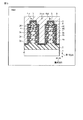
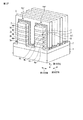
図1は、不揮発性半導体記憶装置の斜視図、図2は、図1の平面図である。図3は、図2のIII−III線に沿う断面図である。
1. First embodiment
(1) Structure
FIG. 1 is a perspective view of a nonvolatile semiconductor memory device, and FIG. 2 is a plan view of FIG. 3 is a cross-sectional view taken along line III-III in FIG.
半導体基板1は、例えば、シリコン基板である。下地絶縁層2は、例えば、酸化シリコン層であり、半導体基板1上に配置される。
The
フィン型積層構造Fin1,Fin2は、下地絶縁層2上に配置される。フィン型積層構造Fin1,Fin2の各々は、例えば、半導体基板1の表面に垂直な第1の方向に積み重ねられる複数(本例では、4つ)のアクティブエリア層3a,3b,3c,3dを有する。また、フィン型積層構造Fin1,Fin2は、半導体基板1の表面に平行な第2の方向に延び、第1及び第2の方向に交差する第3の方向に並ぶ。
The fin-type stacked structures Fin <b> 1 and Fin <b> 2 are disposed on the
アクティブエリア層3a,3b,3c,3dは、例えば、半導体層である。アクティブエリア層3a,3b,3c,3dは、単結晶状態であるのが望ましいが、多結晶状態や、アモルファス状態などであってもよい。
The
アクティブエリア層3a,3b,3c,3dは、例えば、層間絶縁層4a,4b,4c,4dにより互いに絶縁される。但し、アクティブエリア層3a,3b,3c,3dは、互いに絶縁されていればよいので、例えば、空洞により互いに絶縁されていてもよい。
The
本例では、4つのアクティブエリア層3a,3b,3c,3dを積み重ねているが、フィン型積層構造Fin1,Fin2内のアクティブエリア層の数は、これに限定されることはない。フィン型積層構造Fin1,Fin2内のアクティブエリア層の数が多いほど、不揮発性半導体記憶装置のメモリ容量の増大にとっては望ましい。
In this example, four
メモリセルMCは、アクティブエリア層3a,3b,3c,3dの第3の方向の側面上に配置される。例えば、メモリストリングNa,Nb,Nc,Ndは、アクティブエリア層3a,3b,3c,3d上に配置される。メモリストリングNa,Nb,Nc,Ndの各々は、第2の方向に直列接続される複数のメモリセルMCを含む。
Memory cell MC is arranged on the side surface in the third direction of
メモリストリングNa,Nb,Nc,Ndは、複数のメモリセルMCの両端に1つずつ接続される2つの選択トランジスタを備えていてもよい。 The memory strings Na, Nb, Nc, and Nd may include two selection transistors that are connected to both ends of the plurality of memory cells MC one by one.
メモリセルMCは、例えば、アクティブエリア層3a,3b,3c,3dの第3の方向の側面上に配置されるゲート積層構造を備える。ゲート積層構造は、ブロック絶縁層(IPD層)6、電荷蓄積層(フローティングゲート電極)7、トンネル絶縁層8、及び、コントロールゲート電極(ワード線)9の順で積み重ねられる積層構造を含む。
The memory cell MC includes, for example, a gate stacked structure disposed on the side surfaces in the third direction of the
ここで、ブロック絶縁層6とは、書き込み/消去において、アクティブエリア層3a,3b,3c,3dと電荷蓄積層7との間の電荷の移動をブロックする絶縁層のことである。本例では、ブロック絶縁層6は、チャネルとしてのアクティブエリア層3a,3b,3c,3dに接触するため、ゲート絶縁層としても機能する。
Here, the
また、トンネル絶縁層8とは、書き込み/消去において、電荷蓄積層7とコントロールゲート電極9との間で、FNトンネル現象による電荷の移動を行う絶縁層のことである。従って、トンネル絶縁層8の酸化膜換算膜厚(EOT:Equivalent Oxide Thickness)は、ブロック絶縁層6の酸化膜換算膜厚よりも小さいことが必要条件となる。
The
このように、ブロック絶縁層6は、アクティブエリア層3a,3b,3c,3d側に配置され、トンネル絶縁層8は、コントロールゲート電極9側に配置される。
Thus, the
本例では、アクティブエリア層3a,3b,3c,3dの第3の方向の幅は、層間絶縁層4a,4b,4c,4dの第3の方向の幅よりも狭い。これにより、電荷蓄積層7は、層間絶縁層4a,4b,4c,4d間の凹部内に配置され、第1の方向においてメモリセルMCごとに分断される。
In this example, the width of the
ハードマスク層5は、最上層である層間絶縁層4d上に配置される。ハードマスク層5は、フィン型積層構造Fin1,Fin2を形成するときのマスクとなると共に、電荷蓄積層7を第2の方向においてメモリセルMCごとに分断するときのマスクとなる。
The
例えば、電荷蓄積層7を第2の方向においてメモリセルMCごとに分断するとき、ハードマスク層5の第3の方向の幅W1は、アクティブエリア層3a,3b,3c,3dの第3の方向の幅と、ブロック絶縁層6の第3の方向の幅の2倍と、の合計W2よりも狭くする。これにより、コントロールゲート電極9をライン&スペースにパターニングするとき、電荷蓄積層7も分断される。
For example, when the
コントロールゲート電極9は、フィン型積層構造Fin1,Fin2間のスペースを満たす。但し、コントロールゲート電極9は、トンネル絶縁層8を覆うように形成されていれば、フィン型積層構造Fin1,Fin2間のスペースを満たしていなくてもよい。
The
コントロールゲート電極9は、フィン型積層構造Fin1,Fin2の第3の方向の側面上においては、第1の方向に延び、第1の方向に並ぶ複数のメモリセルMCに共有される。また、コントロールゲート電極9は、フィン型積層構造Fin1,Fin2上からみたときは、第3の方向に延びる。
The
(2) 材料例
次に、図1乃至図3の構造の各要素を構成する材料例を説明する。
(2) Material examples
Next, examples of materials constituting each element of the structure shown in FIGS. 1 to 3 will be described.
上述の不揮発性半導体記憶装置を構成する材料については、半導体メモリの各世代に応じた最適な材料を適宜選択することができるが、以下では、最もよく使用される材料例を説明する。 As the material constituting the above-described nonvolatile semiconductor memory device, an optimal material can be appropriately selected according to each generation of the semiconductor memory. Hereinafter, an example of the most frequently used material will be described.
アクティブエリア層3a,3b,3c,3dは、例えば、シリコン層である。シリコン層は、単結晶状態であるのが望ましいが、多結晶状態や、アモルファス状態などであってもよい。また、アクティブエリア層3a,3b,3c,3dは、例えば、Geなどの半導体層や、SiGeなどの化合物半導体層であってもよい。
The
下地絶縁層2及び層間絶縁層4a,4b,4c,4dは、例えば、酸化シリコン層である。層間絶縁層4a,4b,4c,4dは、例えば、酸化シリコン層、窒化シリコン層など、を含む積層構造であってもよい。
The
ハードマスク層5は、層間絶縁層4a,4b,4c,4dと異なる絶縁層、例えば、窒化アルミニウム層である。
The
ブロック絶縁層6及びトンネル絶縁層8は、例えば、酸化シリコン層、窒化シリコン層など、である。ブロック絶縁層6及びトンネル絶縁層8は、酸窒化シリコン層や、酸化シリコン層と窒化シリコン層との組み合わせなど、とすることもできる。
The
ブロック絶縁層6及びトンネル絶縁層8は、酸化ハフニウム層(HfO2)、酸化アルミニウム層(Al2O3)、酸化ランタンアルミニウム層(LaAlO3)、酸化ランタンアルミニウムシリコン層(LaAlSiO)、及び、これらの組成比を変化させた材料など、であってもよい。
The
ブロック絶縁層6及びトンネル絶縁層8は、シリコンナノ粒子や、金属イオンなどを含んでいてもよい。
The
電荷蓄積層7及びコントロールゲート電極9は、例えば、導電性シリコン層を含んでいるのが一般的である。但し、加工が可能であることを条件に、半導体メモリの各世代に応じた最適な材料を適宜選択することができる。
The
例えば、電荷蓄積層7及びコントロールゲート電極9は、タンタルナイトライド(TaN)、タンタルカーバイト(TaC)、チタンナイトライド(TiN)など、のような金属化合物であってもよい。また、電荷蓄積層7及びコントロールゲート電極9は、金属的な電気伝導特性を示す、V、Cr、Mn、Y、Mo、Ru、Rh、Hf、Ta、W、Ir、Co、Ti、Er、Pt、Pd、Zr、Gd、Dy、Ho、及び、これらのシリサイドでもよい。
For example, the
(3) 書き込み/消去、及び、読み出し
第1の実施例の特徴は、書き込み/消去において、電荷蓄積層7とコントロールゲート電極9との間で電荷の移動を行うことにある。そのため、コントロールゲート電極8に接触するトンネル絶縁層8の酸化膜換算膜厚は、アクティブエリア層3a,3b,3c,3dに接触するブロック絶縁層6の酸化膜換算膜厚よりも小さい。
(3) Write / erase and read
The feature of the first embodiment resides in that charges are transferred between the
図4は、書き込み/消去の様子を示している。 FIG. 4 shows a state of writing / erasing.
書き込み/消去においては、例えば、アクティブエリア層3dに電位V1を印加し、コントロールゲート電極9に電位V2を印加することにより、電荷蓄積層7とコントロールゲート電極9との間で、トンネル絶縁層8を介して電荷の移動(Ie)が実行される。
In writing / erasing, for example, the potential V1 is applied to the
例えば、V1>V2の関係にしたとき、電子がコントロールゲート電極9からトンネル絶縁層8を介して電荷蓄積層7に注入される。この時、ブロック絶縁層6の酸化膜換算膜厚は、トンネル絶縁層8の酸化膜換算膜厚よりも大きいため、アクティブエリア層3dと電荷蓄積層7との間の電荷の移動はブロックされる。
For example, when the relationship of V1> V2 is established, electrons are injected from the
また、V1<V2の関係にしたとき、電子が電荷蓄積層7からトンネル絶縁層8を介してコントロールゲート電極9に放出される。この時、ブロック絶縁層6の酸化膜換算膜厚は、トンネル絶縁層8の酸化膜換算膜厚よりも大きいため、アクティブエリア層3dと電荷蓄積層7との間の電荷の移動はブロックされる。
Further, when the relationship of V1 <V2 is established, electrons are emitted from the
図5は、読み出しの様子を示している。 FIG. 5 shows a state of reading.
読み出しにおいては、例えば、コントロールゲート電極9に読み出し電位Vreadを印加することにより、メモリセルのデータ(電荷蓄積層7内の電荷量)に応じた読み出し電流Irがアクティブエリア層(チャネル)3dに流れる。読み出しは、この読み出し電流Irをセンスアンプにより検出することにより行われる。
In reading, for example, by applying a read potential Vread to the
本例によれば、書き込み/消去の繰り返しにより、トンネル絶縁層8にダメージ(欠陥)が発生しても、以下の2つの点で従来よりも有利となる。
According to this example, even if damage (defect) occurs in the
第一に、トンネル絶縁層8の欠陥に電荷がトラップされたとしても、トンネル絶縁層8は、チャネルとしてのアクティブエリア層3a,3b,3c,3dから離れた位置にあるため、それがメモリセルの閾値電圧に与える影響を小さくすることができる。
First, even if charges are trapped by defects in the
第二に、トンネル絶縁層8から電荷がデトラップされたとしても、その電荷は、コントロールゲート電極9に放出されるため、アクティブエリア層3a,3b,3c,3dを流れるチャネル電流に影響を与えることがない。
Second, even if charges are detrapped from the
このため、誤読み出しを防止し、不揮発性半導体記憶装置の信頼性を向上させることができる。 Therefore, erroneous reading can be prevented and the reliability of the nonvolatile semiconductor memory device can be improved.
第一の点について考察する。 Consider the first point.
例えば、トンネル絶縁層8にトラップされた電子の持つ電荷ΔQが、メモリセルの閾値電圧に与える影響は、クーロンの法則により、
ΔQ=CΔV …(1)
のΔVに相当する。但し、Cは静電容量である。
For example, the influence that the charge ΔQ of the electrons trapped in the
ΔQ = CΔV (1)
Of ΔV. However, C is a capacitance.
(1)式を変形すると、
ΔV=ΔQ/C …(2)
となる。
When transforming equation (1),
ΔV = ΔQ / C (2)
It becomes.
C=εS/dを(2)式に代入すると、
ΔV=(ΔQ×d)/εS …(3)
となる。
Substituting C = εS / d into equation (2),
ΔV = (ΔQ × d) / εS (3)
It becomes.
(3)式は、メモリセルの閾値電圧に与える影響ΔVが、トンネル絶縁層8内にトラップされた電子とチャネルとしてのアクティブエリア層3a,3b,3c,3dとの間の距離dに比例することを意味する。但し、εは、トンネル絶縁層8内にトラップされた電子とチャネルとしてのアクティブエリア層3a,3b,3c,3dとの間の絶縁物の誘電率である。
In the expression (3), the influence ΔV on the threshold voltage of the memory cell is proportional to the distance d between the electrons trapped in the
この考察から分かることは、トラップされた電子の位置がチャネルとしてのアクティブエリア層3a,3b,3c,3dから遠ざかることにより、そのトラップされた電子がメモリセルの閾値電圧に与える影響を小さくすることができる、ということである。
It can be seen from this consideration that the influence of the trapped electrons on the threshold voltage of the memory cell is reduced by moving the trapped electrons away from the
(4) 製造方法
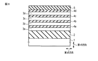
図1乃至図3の構造を製造する方法の例を説明する。
(4) Manufacturing method
An example of a method for manufacturing the structure of FIGS. 1 to 3 will be described.
まず、図6に示すように、例えば、面方位(100)及び比抵抗10〜20Ωcmを有する第1の導電型(例えば、P型)の半導体基板(例えば、シリコン基板)1を用意する。この半導体基板1上に、下地絶縁層(例えば、酸化シリコン層)2、層間絶縁層(例えば、酸化シリコン層)4a,4b,4c,4d、及び、アクティブエリア層(例えば、単結晶シリコン層)3a,3b,3c,3dの積層構造を形成する。
First, as shown in FIG. 6, for example, a first conductivity type (for example, P type) semiconductor substrate (for example, a silicon substrate) 1 having a plane orientation (100) and a specific resistance of 10 to 20 Ωcm is prepared. On this
また、最上層である層間絶縁層4d上に、ハードマスク層(例えば、窒化アルミニウム層)5を形成する。
A hard mask layer (for example, an aluminum nitride layer) 5 is formed on the uppermost
次に、図7に示すように、例えば、ハードマスク層5をマスクにして、異方性エッチングにより、この積層構造をエッチングする。その結果、第2の方向に延び、第3の方向に並ぶ複数のフィン型積層構造Fin1,Fin2が形成される。
Next, as shown in FIG. 7, for example, the laminated structure is etched by anisotropic etching using the
次に、図8に示すように、例えば、ウェットエッチングにより、アクティブエリア層3a,3b,3c,3d及びハードマスク層5を、それぞれ、選択的にシュリンクする。即ち、アクティブエリア層3a,3b,3c,3dの第3の方向の幅、及び、ハードマスク層5の第3の方向の幅は、それぞれ、層間絶縁層4a,4b,4c,4dの第3の方向の幅よりも狭くなる。
Next, as shown in FIG. 8, the
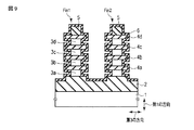
次に、図9に示すように、例えば、CVD法により、フィン型積層構造Fin1,Fin2を覆うブロック絶縁層6を形成する。ブロック絶縁層6は、アクティブエリア層3a,3b,3c,3dの第3の方向に面する表面、及び、層間絶縁層4a,4b,4c,4dの凸部を覆う。
Next, as shown in FIG. 9, for example, the
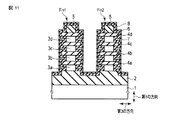
次に、図10に示すように、例えば、CVD法により、フィン型積層構造Fin1,Fin2を覆う第1の導電体を形成した後、第1の導電体を選択的にシュリンクすることにより、第1の導電体を備える電荷蓄積層(フローティングゲート電極)7を形成する。電荷蓄積層7は、層間絶縁層4a,4b,4c,4d間の凹部内に満たされる。
Next, as shown in FIG. 10, for example, a first conductor covering the fin-type stacked structures Fin <b> 1 and Fin <b> 2 is formed by a CVD method, and then the first conductor is selectively shrunk to form a first conductor. A charge storage layer (floating gate electrode) 7 having one conductor is formed. The
次に、図11に示すように、例えば、CVD法により、フィン型積層構造Fin1,Fin2を覆うトンネル絶縁層8を形成する。トンネル絶縁層8は、少なくとも、電荷蓄積層7の第3の方向に面する表面を覆っていればよい。このため、トンネル絶縁層8は、例えば、熱酸化などの方法により、電荷蓄積層7の第3の方向に面する表面のみを覆っていてもよい。
Next, as shown in FIG. 11, for example, a
次に、図12に示すように、例えば、CVD法により、フィン型積層構造Fin1,Fin2を覆い、かつ、フィン型積層構造Fin1,Fin2間のスペースを満たす第2の導電体を形成する。 Next, as shown in FIG. 12, a second conductor that covers the fin-type stacked structures Fin1 and Fin2 and fills the space between the fin-type stacked structures Fin1 and Fin2 is formed by, eg, CVD.
この後、例えば、レジスト層をマスクにして、異方性エッチングにより、第2の導電体を、第3の方向に延びるライン&スペースパターンにパターニングする。その結果、第2の導電体を備えるコントロールゲート電極(ワード線)9が形成される。 Thereafter, for example, the second conductor is patterned into a line and space pattern extending in the third direction by anisotropic etching using the resist layer as a mask. As a result, a control gate electrode (word line) 9 including the second conductor is formed.
このパターニングにおいては、ハードマスク層5をマスクとすることにより、電荷蓄積層7の分断も同時に行われる。
In this patterning, the
以上のステップにより、図1乃至図3の構造を得ることができる。 Through the above steps, the structure of FIGS. 1 to 3 can be obtained.
(5) まとめ
以上、第1の実施例によれば、ブロック絶縁層6が、アクティブエリア層3a,3b,3c,3d側に配置され、トンネル絶縁層8が、コントロールゲート電極9側に配置されることにより、不揮発性半導体記憶装置の信頼性を向上させることができる。
(5) Summary
As described above, according to the first embodiment, the
2. 第2の実施例
(1) 構造
図13は、不揮発性半導体記憶装置の斜視図、図14は、図13の平面図である。図15は、図14のXV−XV線に沿う断面図である。
2. Second embodiment
(1) Structure
FIG. 13 is a perspective view of the nonvolatile semiconductor memory device, and FIG. 14 is a plan view of FIG. 15 is a cross-sectional view taken along line XV-XV in FIG.
第2の実施例は、第1の実施例の変形例である。 The second embodiment is a modification of the first embodiment.
第2の実施例の構造が第1の実施例の構造と異なる点は、メモリセルMCのブロック絶縁層6のレイアウトにある。
The structure of the second embodiment is different from the structure of the first embodiment in the layout of the
即ち、第1の実施例では、図1乃至図3に示すように、ブロック絶縁層6は、層間絶縁層4a,4b,4c,4dの第3の方向の端部を覆い、かつ、アクティブエリア層(半導体層)3a,3b,3c,3d上に配置される複数のメモリセルMCに共有される。
That is, in the first embodiment, as shown in FIGS. 1 to 3, the
これに対し、第2の実施例では、図13至図15に示すように、ブロック絶縁層6は、層間絶縁層4a,4b,4c,4d間の凹部内のアクティブエリア層3a,3b,3c,3dの第3の方向に面する表面上のみに配置される。
On the other hand, in the second embodiment, as shown in FIGS. 13 to 15, the
この場合、電荷蓄積層7の第1の方向の幅W3は、アクティブエリア層3a,3b,3c,3dの第1の方向の幅W4と実質的に等しくできる。これは、アクティブエリア層3a,3b,3c,3dと電荷蓄積層7との対向面積の増加により、書き込み/消去におけるメモリセルMCのカップリング比が向上することを意味する。
In this case, the width W3 in the first direction of the
従って、第2の実施例によれば、書き込み/消去において、トンネル絶縁層8に高い電界が印加されることにより、電荷蓄積層7とコントロールゲート電極9との間の電荷の移動が多くなり、書き込み/消去効率が向上する。
Therefore, according to the second embodiment, when a high electric field is applied to the
その他の点については、第1の実施例と同じであるため、図13乃至図15において、図1乃至図3と同じ要素には同じ符号を付すことにより、その詳細な説明を省略する。 Since the other points are the same as those of the first embodiment, in FIG. 13 to FIG. 15, the same elements as those of FIG. 1 to FIG.
(2) 材料例
図13乃至図15の構造の各要素を構成する材料例については、第1の実施例で説明した材料をそのまま使用可能であるため、ここでの説明を省略する。
(2) Material examples
With respect to the material examples constituting each element of the structure shown in FIGS. 13 to 15, the materials described in the first embodiment can be used as they are, and thus description thereof is omitted here.
(3) 書き込み/消去、及び、読み出し
図13乃至図15の構造を用いた書き込み/消去、及び、読み出しについては、第1の実施例で説明した動作をそのまま適用可能であるため、ここでの説明を省略する。
(3) Write / erase and read
Regarding the writing / erasing and reading using the structure of FIGS. 13 to 15, the operation described in the first embodiment can be applied as it is, and thus the description thereof is omitted here.
(4) 製造方法
図13乃至図15の構造を製造する方法の例を説明する。
(4) Manufacturing method
An example of a method for manufacturing the structure of FIGS. 13 to 15 will be described.
まず、図16に示すように、アクティブエリア層3a,3b,3c,3d及びハードマスク層5をシュリンクするまでのプロセスを、第1の実施例(図6乃至図8参照)と同様に行う。
First, as shown in FIG. 16, the process until the
次に、図17に示すように、アクティブエリア層3a,3b,3c,3dの第3の方向に面する表面上に、ブロック絶縁層6を形成する。
Next, as shown in FIG. 17, the
ブロック絶縁層6は、例えば、熱酸化、プラズマ酸化などの酸化処理、又は、熱窒化、プラズマ窒化などの窒化処理により、アクティブエリア層3a,3b,3c,3dの第3の方向に面する表面上のみに形成するのが望ましい。
The
この後、第1の実施例(図10乃至図12参照)と同様のプロセスを行えば、図13乃至図15の構造を得ることができる。 Thereafter, by performing a process similar to that of the first embodiment (see FIGS. 10 to 12), the structures of FIGS. 13 to 15 can be obtained.
(5) まとめ
以上、第2の実施例によれば、第1の実施例と同様に、不揮発性半導体記憶装置の信頼性を向上させることができる。また、ブロック絶縁層6が、電荷蓄積層7を配置するエリアを狭めることがないため、書き込み/消去効率を向上させることができる。
(5) Summary
As described above, according to the second embodiment, similarly to the first embodiment, the reliability of the nonvolatile semiconductor memory device can be improved. Further, since the
3. 第3の実施例
(1) 構造
図18は、不揮発性半導体記憶装置の斜視図、図19は、図18の平面図である。図20は、図19のXX−XX線に沿う断面図である。
3. Third embodiment
(1) Structure
18 is a perspective view of the nonvolatile semiconductor memory device, and FIG. 19 is a plan view of FIG. 20 is a cross-sectional view taken along line XX-XX in FIG.
第3の実施例も、第1の実施例の変形例である。 The third embodiment is also a modification of the first embodiment.
第3の実施例の構造が第1の実施例の構造と異なる点は、層間絶縁層4a,4b,4c,4dの第3の方向の端部における層間絶縁層4a,4b,4c,4dの第1の方向の幅W5が、アクティブエリア層3a,3b,3c,3d間又は上における層間絶縁層4a,4b,4c,4dの第1の方向の幅W6よりも狭い点にある。
The structure of the third embodiment is different from the structure of the first embodiment in that the
即ち、第1の実施例では、図1乃至図3に示すように、層間絶縁層4a,4b,4c,4dの第1の方向の幅は、実質的に等しいのに対し、第3の実施例では、図18至図20に示すように、層間絶縁層4a,4b,4c,4dの第1の方向の幅は、フィン型積層構造Fin1、Fin2の中央部と第3の方向の端部とで異なる。
That is, in the first embodiment, as shown in FIGS. 1 to 3, the widths in the first direction of the
この場合、ブロック絶縁層6が、層間絶縁層4a,4b,4c,4dの第3の方向の端部(凸部)を覆っていても、電荷蓄積層7の第1の方向の幅W3は、アクティブエリア層3a,3b,3c,3dの第1の方向の幅W4と実質的に等しくできる。これにより、アクティブエリア層3a,3b,3c,3dと電荷蓄積層7との対向面積の増加により、書き込み/消去におけるメモリセルMCのカップリング比を向上させることができる。
In this case, even if the
従って、第3の実施例によれば、書き込み/消去において、トンネル絶縁層8に高い電界が印加されることにより、電荷蓄積層7とコントロールゲート電極9との間の電荷の移動が多くなり、書き込み/消去効率が向上する。
Therefore, according to the third embodiment, when a high electric field is applied to the
その他の点については、第1の実施例と同じであるため、図18乃至図20において、図1乃至図3と同じ要素には同じ符号を付すことにより、その詳細な説明を省略する。 Since the other points are the same as in the first embodiment, the same elements as those in FIGS. 1 to 3 are denoted by the same reference numerals in FIGS. 18 to 20 and detailed description thereof will be omitted.
(2) 電荷蓄積層とアクティブエリア層の関係
図21は、図20の領域Xを詳細に示している。
(2) Relationship between charge storage layer and active area layer
FIG. 21 shows the region X of FIG. 20 in detail.
ブロック絶縁層6が、アクティブエリア層3a,3b,3c,3d側に配置され、トンネル絶縁層8が、コントロールゲート電極9側に配置される場合、ブロック絶縁層6を、層間絶縁層4a,4b,4c,4d間の凹部内に形成しなければならない。
When the
しかし、ブロック絶縁層6は、一般的に、トンネル絶縁層8よりも厚い。また、ブロック絶縁層6に高誘電体(high-k絶縁層)を用いるときは、物理膜厚(physical thickness)がさらに大きくなる。このため、電荷蓄積層7を配置するエリアを拡大し、電荷蓄積層7の第1の方向の幅を広げるためには、第3の実施例の構造は、非常に有効である。
However, the
ここでは、第3の実施例を採用した場合において、電荷蓄積層7の第1の方向の幅とアクティブエリア層3a,3b,3c,3dの第1の方向の幅との望ましい関係について説明する。
Here, when the third embodiment is adopted, a desirable relationship between the width of the
まず、層間絶縁層4a,4b,4c,4dの第3の方向の端部における層間絶縁層4a,4b,4c,4dの第1の方向の幅W5は、電荷蓄積層(フローティングゲート電極)7を互いに絶縁するため、零にならないこと、例えば、1nm以上であるのが望ましい。
First, the width W5 in the first direction of the
従って、W5>0、望ましくは、W5≧1nmである。 Therefore, W5> 0, preferably W5 ≧ 1 nm.
tsh/oxは、層間絶縁層4a,4b,4c,4dのシュリンク処理、又は、アクティブエリア層3a,3b,3c,3dの酸化処理により形成される量である。
tsh / ox is an amount formed by shrink processing of the
即ち、アクティブエリア層3a,3b,3c,3d間又は上における層間絶縁層4a,4b,4c,4dの第1の方向の幅をW6とする場合、tsh/oxが、層間絶縁層4a,4b,4c,4dのシュリンク量に相当するとき、W5=W6−2×tsh/ox(シュリンク量)の関係が成立する。また、tsh/oxが、アクティブエリア層3a,3b,3c,3dの酸化量に相当するとき、W6=W5+2×tsh/ox(酸化量)の関係が成立する。
That is, when the width in the first direction of the
次に、書き込み/消去の観点から、メモリセルのカップリング比を向上させるためには、電荷蓄積層7の第1の方向の幅tfは、アクティブエリア層3a,3b,3c,3dの第1の方向の幅tcと同じ又はそれよりも小さいことが必要である。
Next, in order to improve the coupling ratio of the memory cell from the viewpoint of writing / erasing, the width tf in the first direction of the
即ち、tf≦tc…(1)
である。
That is, tf ≦ tc (1)
It is.
なぜなら、tf>tcになると、アクティブエリア層3a,3b,3c,3dと電荷蓄積層7との対向面積が、電荷蓄積層7とコントロールゲート電極9との対向面積よりも小さくなり、カップリング比が低下するためである。
This is because when tf> tc, the facing area between the
また、電荷蓄積層7内により多くの電荷を蓄積するという観点からは、電荷蓄積層7の体積はできるだけ大きいのが望ましい。従って、tf≦tcという範囲内において、電荷蓄積層7の体積を最も大きくできる条件は、
tf=tc…(2)
である。
From the viewpoint of accumulating more charges in the
tf = tc (2)
It is.
即ち、電荷蓄積層7の第1の方向の幅tfは、アクティブエリア層3a,3b,3c,3dの第1の方向の幅tcと実質的に同じであるのが望ましい。
That is, it is desirable that the width tf in the first direction of the
ここで、電荷蓄積層7と層間絶縁層4a,4b,4c,4dとの間において、ブロック絶縁層6の第1の方向の幅を、tipdとしたとき、上記(1)式を満足するためには、
tsh/ox≦tipd…(3)
であることが必要である。
Here, when the width of the
tsh / ox ≦ tipd (3)
It is necessary to be.
また、上記(2)式を満足するためには、
tsh/ox=tipd…(4)
であることが必要である。
In order to satisfy the above formula (2),
tsh / ox = tipd (4)
It is necessary to be.
従って、最も望ましい電荷蓄積層とアクティブエリア層との関係、即ち、上記(2)式を満たすためには、上記(4)式を満たすように、図18乃至図20の不揮発性半導体記憶装置を製造することが必要である。 Therefore, in order to satisfy the most desirable relationship between the charge storage layer and the active area layer, that is, the above expression (2), the nonvolatile semiconductor memory device of FIGS. 18 to 20 is satisfied so as to satisfy the above expression (4). It is necessary to manufacture.
(3) 材料例
図18乃至図20の構造の各要素を構成する材料例については、第1の実施例で説明した材料をそのまま使用可能であるため、ここでの説明を省略する。
(3) Material examples
18 to 20, the materials described in the first embodiment can be used as they are, so that the description thereof is omitted here.
(4) 書き込み/消去、及び、読み出し
図18乃至図20の構造を用いた書き込み/消去、及び、読み出しについては、第1の実施例で説明した動作をそのまま適用可能であるため、ここでの説明を省略する。
(4) Write / erase and read
For writing / erasing and reading using the structure of FIGS. 18 to 20, the operation described in the first embodiment can be applied as it is, and thus description thereof is omitted here.
(5) 製造方法
図18乃至図20の構造を製造する方法の例を説明する。
(5) Manufacturing method
An example of a method for manufacturing the structure of FIGS. 18 to 20 will be described.
まず、図22に示すように、例えば、面方位(100)及び比抵抗10〜20Ωcmを有する第1の導電型(例えば、P型)の半導体基板(例えば、シリコン基板)1を用意する。この半導体基板1上に、下地絶縁層(例えば、酸化シリコン層)2、層間絶縁層(例えば、酸化シリコン層)4a,4b,4c,4d、及び、アクティブエリア層(例えば、単結晶シリコン層)3a,3b,3c,3dの積層構造を形成する。
First, as shown in FIG. 22, for example, a first conductivity type (for example, P type) semiconductor substrate (for example, a silicon substrate) 1 having a plane orientation (100) and a specific resistance of 10 to 20 Ωcm is prepared. On this
本例は、第1の実施例の製造方法と比べると、層間絶縁層4a,4b,4c,4dの厚さ(第1の方向の幅)が大きく、アクティブエリア層3a,3b,3c,3dの厚さ(第1の方向の幅)が小さい点に特徴を有する。本例は、アクティブエリア層3a,3b,3c,3dが薄いため、メモリセルの微細化に有利である。
In this example, compared with the manufacturing method of the first example, the thickness (width in the first direction) of the
この後、最上層である層間絶縁層4d上に、ハードマスク層(例えば、窒化アルミニウム層)5を形成する。
Thereafter, a hard mask layer (for example, aluminum nitride layer) 5 is formed on the uppermost
また、例えば、ハードマスク層5をマスクにして、異方性エッチングにより、この積層構造をエッチングする。その結果、第2の方向に延び、第3の方向に並ぶ複数のフィン型積層構造Fin1,Fin2が形成される。
Further, for example, the laminated structure is etched by anisotropic etching using the
次に、図23に示すように、例えば、ウェットエッチングにより、アクティブエリア層3a,3b,3c,3d及びハードマスク層5を、それぞれ、選択的にシュリンクする。即ち、アクティブエリア層3a,3b,3c,3dの第3の方向の幅、及び、ハードマスク層5の第3の方向の幅は、それぞれ、層間絶縁層4a,4b,4c,4dの第3の方向の幅よりも狭くなる。
Next, as shown in FIG. 23, the
次に、図24に示すように、例えば、ウェットエッチングにより、層間絶縁層4a,4b,4c,4dを選択的にシュリンクする。即ち、層間絶縁層4a,4b,4c,4dの第3の方向の端部(凸部)において、層間絶縁層4a,4b,4c,4dの第1の方向の幅は、アクティブエリア層3a,3b,3c,3d間又は上における層間絶縁層4a,4b,4c,4dの第1の方向の幅よりも2×tsh/ox狭くなる。
Next, as shown in FIG. 24, the
このステップにより、メモリセルの電荷蓄積層を配置するエリア、即ち、層間絶縁層4a,4b,4c,4d間の凹部の第1の方向の幅、を広げることができる。
By this step, the area where the charge storage layer of the memory cell is arranged, that is, the width in the first direction of the recess between the interlayer insulating
この後、第1の実施例(図9乃至図12参照)と同様のプロセスを行えば、図18乃至図20の構造を得ることができる。 Thereafter, by performing the same process as in the first embodiment (see FIGS. 9 to 12), the structures of FIGS. 18 to 20 can be obtained.
図18乃至図20の構造は、以下の製造方法により形成することも可能である。 The structure of FIGS. 18 to 20 can also be formed by the following manufacturing method.
まず、図25に示すように、アクティブエリア層3a,3b,3c,3d及びハードマスク層5をシュリンクし、フィン型積層構造Fin1,Fin2を覆うブロック絶縁層6を形成するまでのプロセスを、第1の実施例(図6乃至図9参照)と同様に行う。
First, as shown in FIG. 25, the
次に、図26に示すように、例えば、酸素雰囲気中でアニールを行い、アクティブエリア層3a,3b,3c,3dの第1の方向の端部、即ち、アクティブエリア層3a,3b,3c,3dのうち層間絶縁層4a,4b,4c,4dに接触する部分を、酸化する。但し、層間絶縁層4a,4b,4c,4dは、酸素を含む絶縁層(例えば、酸化シリコン層)とする。
Next, as shown in FIG. 26, for example, annealing is performed in an oxygen atmosphere, and ends in the first direction of the
このステップにより、アクティブエリア層3a,3b,3c,3dの厚さ、即ち、第1の方向の幅を、2×tsh/oxだけ狭めることができる。
By this step, the thickness of the
この後、第1の実施例(図10乃至図12参照)と同様のプロセスを行えば、図18乃至図20の構造を得ることができる。 Thereafter, by performing the same process as in the first embodiment (see FIGS. 10 to 12), the structures of FIGS. 18 to 20 can be obtained.
(6) まとめ
以上、第3の実施例によれば、第1の実施例と同様に、不揮発性半導体記憶装置の信頼性を向上させることができる。また、ブロック絶縁層6が、層間絶縁層4a,4b,4c,4d間の凸部を覆っていても、電荷蓄積層7の第1の方向の幅を、アクティブエリア層3a,3b,3c,3dの第1の方向の幅と実質的に同じにすることができるため、書き込み/消去効率を向上させることができる。さらに、アクティブエリア層3a,3b,3c,3dを薄くできるため、メモリセルの微細化にも有利である。
(6) Summary
As described above, according to the third embodiment, similarly to the first embodiment, the reliability of the nonvolatile semiconductor memory device can be improved. Even if the
4. 第4の実施例
(1) 構造
図27は、不揮発性半導体記憶装置の斜視図、図28は、図27の平面図である。図29は、図28のXXIX−XXIX線に沿う断面図である。
4). Fourth embodiment
(1) Structure
27 is a perspective view of the nonvolatile semiconductor memory device, and FIG. 28 is a plan view of FIG. 29 is a cross-sectional view taken along line XXIX-XXIX in FIG.
第4の実施例は、第1乃至第3の実施例と比べると、メモリセルMCの構造が大きく異なっている。 The fourth embodiment is greatly different from the first to third embodiments in the structure of the memory cell MC.
即ち、第1乃至第3の実施例では、メモリセルMCは、電気的にフローティング状態の導電層(フローティングゲート電極)を電荷蓄積層7として用いるのに対し、第4の実施例では、メモリセルMCは、電荷をトラップする機能を有する絶縁層(電荷トラップ層)を電荷蓄積層7として用いる。
That is, in the first to third embodiments, the memory cell MC uses an electrically floating conductive layer (floating gate electrode) as the
半導体基板1は、例えば、シリコン基板である。下地絶縁層2は、例えば、酸化シリコン層であり、半導体基板1上に配置される。
The
フィン型積層構造Fin1,Fin2は、下地絶縁層2上に配置される。フィン型積層構造Fin1,Fin2の各々は、例えば、半導体基板1の表面に垂直な第1の方向に積み重ねられる複数(本例では、4つ)のアクティブエリア層3a,3b,3c,3dを有する。また、フィン型積層構造Fin1,Fin2は、半導体基板1の表面に平行な第2の方向に延び、第1及び第2の方向に交差する第3の方向に並ぶ。
The fin-type stacked structures Fin <b> 1 and Fin <b> 2 are disposed on the
アクティブエリア層3a,3b,3c,3dは、例えば、半導体層である。アクティブエリア層3a,3b,3c,3dは、単結晶状態であるのが望ましいが、多結晶状態や、アモルファス状態などであってもよい。
The
アクティブエリア層3a,3b,3c,3dは、例えば、層間絶縁層4a,4b,4c,4dにより互いに絶縁される。但し、アクティブエリア層3a,3b,3c,3dは、互いに絶縁されていればよいので、例えば、空洞により互いに絶縁されていてもよい。
The
本例では、4つのアクティブエリア層3a,3b,3c,3dを積み重ねているが、フィン型積層構造Fin1,Fin2内のアクティブエリア層の数は、これに限定されることはない。フィン型積層構造Fin1,Fin2内のアクティブエリア層の数が多いほど、不揮発性半導体記憶装置のメモリ容量の増大にとっては望ましい。
In this example, four
メモリセルMCは、アクティブエリア層3a,3b,3c,3dの第3の方向の側面上に配置される。例えば、メモリストリングNa,Nb,Nc,Ndは、アクティブエリア層3a,3b,3c,3d上に配置される。メモリストリングNa,Nb,Nc,Ndの各々は、第2の方向に直列接続される複数のメモリセルMCを含む。
Memory cell MC is arranged on the side surface in the third direction of
メモリストリングNa,Nb,Nc,Ndは、複数のメモリセルMCの両端に1つずつ接続される2つの選択トランジスタを備えていてもよい。 The memory strings Na, Nb, Nc, and Nd may include two selection transistors that are connected to both ends of the plurality of memory cells MC one by one.
メモリセルMCは、例えば、アクティブエリア層3a,3b,3c,3dの第3の方向の側面上に配置されるゲート積層構造を備える。ゲート積層構造は、ブロック絶縁層6、電荷蓄積層(電荷トラップ層)7、トンネル絶縁層8、及び、コントロールゲート電極(ワード線)9の順で積み重ねられる積層構造を含む。
The memory cell MC includes, for example, a gate stacked structure disposed on the side surfaces in the third direction of the
このように、本例においても、第1乃至第3の実施例と同様に、ブロック絶縁層6は、アクティブエリア層3a,3b,3c,3d側に配置され、トンネル絶縁層8は、コントロールゲート電極9側に配置される。
Thus, in this example as well, as in the first to third embodiments, the
本例では、アクティブエリア層3a,3b,3c,3dの第3の方向の幅は、層間絶縁層4a,4b,4c,4dの第3の方向の幅と実質的に同じである。
In this example, the width in the third direction of the
ハードマスク層5は、最上層である層間絶縁層4d上に配置される。ハードマスク層5は、フィン型積層構造Fin1,Fin2を形成するときのマスクとなる。
The
コントロールゲート電極9は、フィン型積層構造Fin1,Fin2間のスペースを満たす。但し、コントロールゲート電極9は、フィン型積層構造Fin1,Fin2間のスペースを満たしていなくてもよい。
The
コントロールゲート電極9は、フィン型積層構造Fin1,Fin2の第3の方向の側面上においては、第1の方向に延び、第1の方向に並ぶ複数のメモリセルMCに共有される。また、コントロールゲート電極9は、フィン型積層構造Fin1,Fin2上からみたときは、第3の方向に延びる。
The
尚、本例においては、ブロック絶縁層6、電荷蓄積層7、及び、トンネル絶縁層8は、コントロールゲート電極9の直下に配置され、フィン型積層構造Fin1,Fin2の第3の方向の側面上においては、第1の方向に延びる。即ち、第1の方向において、複数のメモリセルMCの電荷蓄積層7は、互いに接続される。
In this example, the
本例では、電荷蓄積層7は、電荷トラップ層を用いているため、このように、複数のメモリセルMCの電荷蓄積層7が互いに接続されていても問題ない。
In this example, since the
また、本例においては、第1の方向において、複数のメモリセルMC、即ち、メモリストリングNa,Nb,Nc,Ndの電荷蓄積層7は、互いに分断される。
In this example, in the first direction, the plurality of memory cells MC, that is, the
但し、同様の理由により、第1の方向において、複数のメモリセルMCの電荷蓄積層7は、互いに接続されていてもよい。この場合、コントロールゲート電極9をライン&スペースにパターニングするときに、電荷蓄積層7をパターニングしなければよい。
However, for the same reason, the
(2) 材料例
次に、図27乃至図29の構造の各要素を構成する材料例を説明する。
(2) Material examples
Next, examples of materials constituting each element of the structure shown in FIGS. 27 to 29 will be described.
上述の不揮発性半導体記憶装置を構成する材料については、半導体メモリの各世代に応じた最適な材料を適宜選択することができるが、以下では、最もよく使用される材料例を説明する。 As the material constituting the above-described nonvolatile semiconductor memory device, an optimal material can be appropriately selected according to each generation of the semiconductor memory. Hereinafter, an example of the most frequently used material will be described.
電荷蓄積層7は、例えば、シリコンリッチSiN、シリコンと窒素の組成比x、yが任意であるSixNy、酸窒化シリコン(SiON)、酸化アルミニウム(Al2O3)、酸窒化アルミニウム(AlON)、ハフニア(HfO2)、ハフニウム・アルミネート(HfAlO3)、窒化ハフニア(HfON)、窒化ハフニウム・アルミネート(HfAlON)、ハフニウム・シリケート(HfSiO)、窒化ハフニウム・シリケート(HfSiON)、酸化ランタン(La2O3)及びランタン・アルミネート(LaAlO3)のグループから選択される少なくとも1つである。
The
その他の構成要素の材料例については、第1の実施例で説明した材料をそのまま使用可能であるため、ここでの説明を省略する。 About the material example of another component, since the material demonstrated in the 1st Example can be used as it is, description here is abbreviate | omitted.
(3) 書き込み/消去、及び、読み出し
図27乃至図29の構造を用いた書き込み/消去、及び、読み出しについては、第1の実施例で説明した動作をそのまま適用可能であるため、ここでの説明を省略する。
(3) Write / erase and read
For writing / erasing and reading using the structure of FIGS. 27 to 29, the operation described in the first embodiment can be applied as it is, and thus description thereof is omitted here.
(4) 製造方法
図27乃至図29の構造を製造する方法の例を説明する。
(4) Manufacturing method
An example of a method for manufacturing the structure of FIGS. 27 to 29 will be described.
まず、図30に示すように、フィン型積層構造Fin1,Fin2を形成するまでのプロセスを、第1の実施例(図6及び図7参照)と同様に行う。 First, as shown in FIG. 30, the process up to the formation of the fin-type stacked structures Fin1 and Fin2 is performed in the same manner as in the first embodiment (see FIGS. 6 and 7).
次に、図31に示すように、フィン型積層構造Fin1,Fin2を覆うように、ブロック絶縁層6、電荷蓄積層7、トンネル絶縁層8、及び、コントロールゲート電極9を、それぞれ形成する。
Next, as shown in FIG. 31, a
この後、例えば、レジスト層をマスクにして、異方性エッチングにより、コントロールゲート電極9を、第3の方向に延びるライン&スペースパターンにパターニングする。この時、コントロールゲート電極9と同様に、トンネル絶縁層8、電荷蓄積層7、及び、ブロック絶縁層6を、それぞれ、パターニングしてもよい。
Thereafter, for example, the
以上のステップにより、図27乃至図29の構造を得ることができる。 Through the above steps, the structure of FIGS. 27 to 29 can be obtained.
(5) まとめ
以上、第4の実施例によれば、第1の実施例と同様に、不揮発性半導体記憶装置の信頼性を向上させることができる。また、メモリセルMCの電荷蓄積層7として、電荷トラップ層を用いることにより、不揮発性半導体記憶装置の構造及び製造方法を簡略化することができる。
(5) Summary
As described above, according to the fourth embodiment, similarly to the first embodiment, the reliability of the nonvolatile semiconductor memory device can be improved. Further, by using a charge trap layer as the
5. 適用例
上述の第1乃至第4の実施例を、例えば、VLB (Vertical gate ladder-Bit cost scalable memory)に適用した場合を説明する。
5. Application examples
The case where the first to fourth embodiments described above are applied to, for example, a VLB (Vertical gate ladder-Bit cost scalable memory) will be described.
図32及び図33は、VLBの斜視図を示している。 32 and 33 show perspective views of the VLB.
複数のフィン型積層構造Fin1,Fin2,Fin3の各々は、アクティブエリア層3a,3b,3cを有する。上述の第1及び第4の実施例では、アクティブエリア層の積層数が4層であったが、本例では、アクティブエリア層の積層数が3層である。
Each of the plurality of fin-type stacked structures Fin1, Fin2, and Fin3 includes
VG(Vertical gate)-NANDは、上述の第1乃至第4の実施例で説明したメモリストリングNa、Nb,Nc(図1参照)を含む。 VG (Vertical gate) -NAND includes the memory strings Na, Nb, and Nc (see FIG. 1) described in the first to fourth embodiments.
複数のフィン型積層構造Fin1,Fin2,Fin3の第2の方向の両端は、第3の方向に延びる梁11−1,11−2に接続される。梁11−1,11−2は、複数のフィン型積層構造Fin1、Fin2,Fin3と同様に、アクティブエリア層3a,3b,3cを有する。
Both ends of the plurality of fin-type stacked structures Fin1, Fin2, and Fin3 in the second direction are connected to beams 11-1 and 11-2 extending in the third direction. The beams 11-1 and 11-2 have
但し、梁11−1内のアクティブエリア層3a,3b,3cは、低抵抗化のため、不純物領域12a,12b,12cを有し、梁11−2内のアクティブエリア層3a,3b,3cは、低抵抗化のため、不純物領域14a,14b,14cを有する。
However, the
梁11−1,11−2の第3の方向の端部は、複数のメモリストリングNa、Nb,Ncのうちの1つを選択するための機能を備える。 The ends of the beams 11-1 and 11-2 in the third direction have a function for selecting one of the plurality of memory strings Na, Nb, and Nc.
例えば、図22の例では、梁11−1,11−2の第3の方向の端部は、階段形状を有する。また、ビット線BLa,BLb,BLcは、コンタクトプラグ13a,13b,13cを介して、梁11−1内のアクティブエリア3a,3b,3cに、それぞれ、独立に接続される。ソース線SLは、コンタクトプラグ15a,15b,15cを介して、梁11−2内のアクティブエリア3a,3b,3cに、それぞれ、独立に接続される。
For example, in the example of FIG. 22, the ends of the beams 11-1 and 11-2 in the third direction have a step shape. The bit lines BLa, BLb, and BLc are independently connected to the
また、図23の例では、梁11−1,11−2の第3の方向の端部は、アクティブエリア3a,3b,3cに共通に接続される共通半導体層16−1,16−2と、レイヤー選択トランジスタLSTa,LSTb,LSTcとを有する。
In the example of FIG. 23, the end portions of the beams 11-1 and 11-2 in the third direction are connected to the common semiconductor layers 16-1 and 16-2 commonly connected to the
ビット線BLは、コンタクトプラグ17−1を介して、共通半導体層16−1に接続され、ソース線SLは、コンタクトプラグ17−2を介して、共通半導体層16−2に接続される。 The bit line BL is connected to the common semiconductor layer 16-1 via the contact plug 17-1, and the source line SL is connected to the common semiconductor layer 16-2 via the contact plug 17-2.
レイヤー選択トランジスタLSTa,LSTb,LSTcは、選択ゲート電極SGa,SGb,SGcを有する。 The layer selection transistors LSTa, LSTb, and LSTc have selection gate electrodes SGa, SGb, and SGc.
レイヤー選択トランジスタLSTaは、選択ゲート電極SGaにより覆われる最下層としてのアクティブエリア3a内に不純物領域18aを有する。レイヤー選択トランジスタLSTbは、選択ゲート電極SGbにより覆われる中間層としてのアクティブエリア3b内に不純物領域18bを有する。レイヤー選択トランジスタLSTcは、選択ゲート電極SGcにより覆われる最上層としてのアクティブエリア3c内に不純物領域18cを有する。
The layer selection transistor LSTa has an
これにより、複数のメモリストリングNa、Nb,Ncのうちの1つ(フィン型積層構造Fin1,Fin2,Fin3内の1つのアクティブエリア層)を選択することができる。 Thereby, one of the plurality of memory strings Na, Nb, and Nc (one active area layer in the fin-type stacked structures Fin1, Fin2, and Fin3) can be selected.
6. むすび
以上、実施形態によれば、不揮発性半導体記憶装置の高信頼性を図ることができる。
6). Conclusion
As described above, according to the embodiment, high reliability of the nonvolatile semiconductor memory device can be achieved.
本発明のいくつかの実施形態を説明したが、これらの実施形態は、例として提示したものであり、発明の範囲を限定することは意図していない。これら新規な実施形態は、その他の様々な形態で実施されることが可能であり、発明の要旨を逸脱しない範囲で、種々の省略、置き換え、変更を行うことができる。これら実施形態やその変形は、発明の範囲や要旨に含まれるとともに、特許請求の範囲に記載された発明とその均等の範囲に含まれる。 Although several embodiments of the present invention have been described, these embodiments are presented by way of example and are not intended to limit the scope of the invention. These novel embodiments can be implemented in various other forms, and various omissions, replacements, and changes can be made without departing from the scope of the invention. These embodiments and modifications thereof are included in the scope and gist of the invention, and are included in the invention described in the claims and the equivalents thereof.
1: 半導体基板、 2: 下地絶縁層、 3a,3b,3c,3d: アクティブエリア(半導体層)、 4a,4b,4c,4d: 層間絶縁層、 5: ハードマスク層、 6: ブロック絶縁層、 7: 電荷蓄積層、 8: トンネル絶縁層、 9: コントロールゲート電極。 1: semiconductor substrate, 2: underlying insulating layer, 3a, 3b, 3c, 3d: active area (semiconductor layer), 4a, 4b, 4c, 4d: interlayer insulating layer, 5: hard mask layer, 6: block insulating layer, 7: charge storage layer, 8: tunnel insulating layer, 9: control gate electrode.
Claims (5)
前記半導体基板の表面に対して垂直な第1の方向に積み重ねられる第1乃至第nの半導体層(nは、2以上の自然数)を有し、前記半導体基板の表面に対して平行な第2の方向に延びる第1の積層構造と、
前記第1乃至第nの半導体層の前記第1及び第2の方向に垂直な第3の方向に面する表面上にそれぞれ配置される第1乃至第nのメモリセルと、
を具備し、
前記第i(iは、1乃至nのうちの1つ)のメモリセルは、前記第iの半導体層の前記第3の方向に面する表面上から、第1の絶縁層、電荷蓄積層、第2の絶縁層、及び、コントロールゲート電極の順に配置される第2の積層構造を備え、
前記第2の絶縁層の酸化膜換算膜厚は、前記第1の絶縁層の酸化膜換算膜厚よりも小さい
不揮発性半導体記憶装置。 A semiconductor substrate;
The first to n-th semiconductor layers (n is a natural number of 2 or more) stacked in a first direction perpendicular to the surface of the semiconductor substrate, and are parallel to the surface of the semiconductor substrate. A first laminated structure extending in the direction of
First to nth memory cells respectively disposed on surfaces of the first to nth semiconductor layers facing a third direction perpendicular to the first and second directions;
Comprising
The i-th (i is one of 1 to n) memory cell includes a first insulating layer, a charge storage layer, a surface of the i-th semiconductor layer facing the third direction, A second insulating layer, and a second laminated structure arranged in the order of the control gate electrode,
A non-volatile semiconductor memory device, wherein the second insulating layer has an equivalent oxide film thickness that is smaller than an oxide film equivalent film thickness of the first insulating layer.
前記第jの層間絶縁層(jは、1乃至(n−1)のうちの1つ)は、前記第j及び第(j+1)の半導体層間に配置され、
前記第jの層間絶縁層の前記第3の方向の第1の幅は、前記第j及び第(j+1)の半導体層の前記第3の方向の第2の幅よりも広い
請求項1に記載の不揮発性半導体記憶装置。 A first to (n-1) th interlayer insulating layer for insulating the first to nth semiconductor layers from each other;
The jth interlayer insulating layer (j is one of 1 to (n−1)) is disposed between the jth and (j + 1) th semiconductor layers,
2. The first width in the third direction of the jth interlayer insulating layer is wider than the second width in the third direction of the jth and (j + 1) th semiconductor layers. Nonvolatile semiconductor memory device.
請求項2に記載の不揮発性半導体記憶装置。 The third width in the first direction of the j-th interlayer insulating layer at the end of the j-th interlayer insulating layer in the third direction is the j-th and (j + 1) th semiconductor layers between the j-th interlayer insulating layers. The nonvolatile semiconductor memory device according to claim 2, wherein the j-th interlayer insulating layer is narrower than a fourth width in the first direction.
請求項1乃至3のいずれか1項に記載の不揮発性半導体記憶装置。 The first insulating layer covers end portions in the third direction of the first to (n−1) th interlayer insulating layers and is provided in common to the first to nth memory cells. The non-volatile semiconductor memory device according to claim 1.
請求項1乃至4のいずれか1項に記載の不揮発性半導体記憶装置。 The i-th memory cell performs charge transfer between the charge storage layer and the control gate electrode in a write / erase operation, and allows a read current to flow in the i-th semiconductor layer in a read operation. 5. The nonvolatile semiconductor memory device according to any one of 1 to 4.
Priority Applications (3)
| Application Number | Priority Date | Filing Date | Title |
|---|---|---|---|
| JP2014041659A JP2015167200A (en) | 2014-03-04 | 2014-03-04 | Non-volatile semiconductor storage device |
| US14/489,700 US9230975B2 (en) | 2014-03-04 | 2014-09-18 | Nonvolatile semiconductor memory device |
| US14/932,532 US9373631B2 (en) | 2014-03-04 | 2015-11-04 | Nonvolatile semiconductor memory device |
Applications Claiming Priority (1)
| Application Number | Priority Date | Filing Date | Title |
|---|---|---|---|
| JP2014041659A JP2015167200A (en) | 2014-03-04 | 2014-03-04 | Non-volatile semiconductor storage device |
Publications (1)
| Publication Number | Publication Date |
|---|---|
| JP2015167200A true JP2015167200A (en) | 2015-09-24 |
Family
ID=54018153
Family Applications (1)
| Application Number | Title | Priority Date | Filing Date |
|---|---|---|---|
| JP2014041659A Pending JP2015167200A (en) | 2014-03-04 | 2014-03-04 | Non-volatile semiconductor storage device |
Country Status (2)
| Country | Link |
|---|---|
| US (2) | US9230975B2 (en) |
| JP (1) | JP2015167200A (en) |
Families Citing this family (6)
| Publication number | Priority date | Publication date | Assignee | Title |
|---|---|---|---|---|
| US9917096B2 (en) * | 2014-09-10 | 2018-03-13 | Toshiba Memory Corporation | Semiconductor memory device and method for manufacturing same |
| CN106847819B (en) * | 2015-12-03 | 2019-10-18 | 上海复旦微电子集团股份有限公司 | Nand flash memory storage unit, nand flash memory and forming method thereof |
| CN107230677B (en) * | 2016-03-24 | 2019-08-16 | 上海复旦微电子集团股份有限公司 | A kind of the data cell array structure and its manufacturing method of nand flash memory |
| CN107516660B (en) * | 2016-06-17 | 2019-10-22 | 上海复旦微电子集团股份有限公司 | Nand flash memory storage unit, nand flash memory and forming method thereof |
| US10707121B2 (en) * | 2016-12-31 | 2020-07-07 | Intel Corporatino | Solid state memory device, and manufacturing method thereof |
| JP7089967B2 (en) * | 2018-07-17 | 2022-06-23 | ルネサスエレクトロニクス株式会社 | Semiconductor devices and their manufacturing methods |
Family Cites Families (31)
| Publication number | Priority date | Publication date | Assignee | Title |
|---|---|---|---|---|
| JP2877103B2 (en) | 1996-10-21 | 1999-03-31 | 日本電気株式会社 | Nonvolatile semiconductor memory device and method of manufacturing the same |
| US7271444B2 (en) * | 2003-12-11 | 2007-09-18 | International Business Machines Corporation | Wrap-around gate field effect transistor |
| KR100674952B1 (en) | 2005-02-05 | 2007-01-26 | 삼성전자주식회사 | 3-dimensional flash memory device and fabrication method thereof |
| US7352018B2 (en) | 2005-07-22 | 2008-04-01 | Infineon Technologies Ag | Non-volatile memory cells and methods for fabricating non-volatile memory cells |
| JP5016832B2 (en) | 2006-03-27 | 2012-09-05 | 株式会社東芝 | Nonvolatile semiconductor memory device and manufacturing method thereof |
| JP2008078404A (en) | 2006-09-21 | 2008-04-03 | Toshiba Corp | Semiconductor memory and manufacturing method thereof |
| JP4760689B2 (en) | 2006-11-30 | 2011-08-31 | セイコーエプソン株式会社 | Manufacturing method of semiconductor device |
| US8779495B2 (en) | 2007-04-19 | 2014-07-15 | Qimonda Ag | Stacked SONOS memory |
| US7714377B2 (en) | 2007-04-19 | 2010-05-11 | Qimonda Ag | Integrated circuits and methods of manufacturing thereof |
| JP2009238874A (en) | 2008-03-26 | 2009-10-15 | Toshiba Corp | Semiconductor memory and method for manufacturing the same |
| US7867831B2 (en) | 2008-05-28 | 2011-01-11 | Hynix Semiconductor Inc. | Manufacturing method of flash memory device comprising gate columns penetrating through a cell stack |
| JP2009295694A (en) | 2008-06-03 | 2009-12-17 | Toshiba Corp | Non-volatile semiconductor storage device and manufacturing method thereof |
| FR2933802B1 (en) | 2008-07-10 | 2010-10-15 | Commissariat Energie Atomique | STRUCTURE AND METHOD FOR PRODUCING A MICROELECTRONIC 3D MEMORY DEVICE OF NAND FLASH TYPE |
| KR20100007229A (en) | 2008-07-11 | 2010-01-22 | 삼성전자주식회사 | Non-volatile memory device and method of fabricating the same |
| KR101478678B1 (en) * | 2008-08-21 | 2015-01-02 | 삼성전자주식회사 | Non-volatile memory device and method of fabricating the same |
| US7994011B2 (en) * | 2008-11-12 | 2011-08-09 | Samsung Electronics Co., Ltd. | Method of manufacturing nonvolatile memory device and nonvolatile memory device manufactured by the method |
| KR101495806B1 (en) * | 2008-12-24 | 2015-02-26 | 삼성전자주식회사 | Non-volatile memory device |
| KR101558851B1 (en) | 2009-01-06 | 2015-10-19 | 삼성전자주식회사 | Nonvolatile memory device and method for operating the same |
| KR101481104B1 (en) * | 2009-01-19 | 2015-01-13 | 삼성전자주식회사 | Nonvolatile memory devices and method for fabricating the same |
| TWI433302B (en) | 2009-03-03 | 2014-04-01 | Macronix Int Co Ltd | Integrated circuit self aligned 3d memory array and manufacturing method |
| JP5456036B2 (en) | 2009-06-12 | 2014-03-26 | 株式会社東芝 | Nonvolatile semiconductor memory device |
| KR101616089B1 (en) * | 2009-06-22 | 2016-04-28 | 삼성전자주식회사 | Three dimensional semiconductor memory device |
| KR101028993B1 (en) | 2009-06-30 | 2011-04-12 | 주식회사 하이닉스반도체 | 3d-nonvolatile memory device and method for fabricating the same |
| KR101584113B1 (en) * | 2009-09-29 | 2016-01-13 | 삼성전자주식회사 | 3 Three Dimensional Semiconductor Memory Device And Method Of Fabricating The Same |
| WO2011114503A1 (en) | 2010-03-19 | 2011-09-22 | 株式会社 東芝 | Nonvolatile semiconductor storage device and method for producing same |
| WO2011114502A1 (en) | 2010-03-19 | 2011-09-22 | 株式会社 東芝 | Nonvolatile semiconductor storage device and method for producing same |
| US8193054B2 (en) * | 2010-06-30 | 2012-06-05 | SanDisk Technologies, Inc. | Ultrahigh density vertical NAND memory device and method of making thereof |
| KR20120077040A (en) * | 2010-12-30 | 2012-07-10 | 에스케이하이닉스 주식회사 | Nonvolatile memory device and method for fabricating the same |
| JP2012234980A (en) | 2011-05-02 | 2012-11-29 | Toshiba Corp | Nonvolatile semiconductor storage device and manufacturing method of the same |
| JP2013239622A (en) | 2012-05-16 | 2013-11-28 | Toshiba Corp | Nonvolatile semiconductor storage device and manufacturing method of the same |
| JP2014179530A (en) | 2013-03-15 | 2014-09-25 | Toshiba Corp | Method for manufacturing non-volatile semiconductor memory device |
-
2014
- 2014-03-04 JP JP2014041659A patent/JP2015167200A/en active Pending
- 2014-09-18 US US14/489,700 patent/US9230975B2/en active Active
-
2015
- 2015-11-04 US US14/932,532 patent/US9373631B2/en active Active
Also Published As
| Publication number | Publication date |
|---|---|
| US9230975B2 (en) | 2016-01-05 |
| US20160056166A1 (en) | 2016-02-25 |
| US9373631B2 (en) | 2016-06-21 |
| US20150255479A1 (en) | 2015-09-10 |
Similar Documents
| Publication | Publication Date | Title |
|---|---|---|
| TWI663715B (en) | String select line gate oxide method for 3d vertical channel nand memory | |
| JP5651415B2 (en) | Nonvolatile semiconductor memory device and manufacturing method thereof | |
| US9502431B2 (en) | Nonvolatile semiconductor memory device and method of manufacturing the same | |
| TWI631692B (en) | Memory device and manufacturing method thereof | |
| US8674429B2 (en) | Gate structure in non-volatile memory device | |
| US8546872B2 (en) | Nonvolatile semiconductor memory device and method of manufacturing the same | |
| US9373631B2 (en) | Nonvolatile semiconductor memory device | |
| TWI549264B (en) | Non-volatile semiconductor memory device | |
| US9087715B2 (en) | Nonvolatile semiconductor memory device and method of manufacturing the same | |
| KR101218447B1 (en) | Semiconductor memory device | |
| US8987088B2 (en) | Method of manufacturing nonvolatile semiconductor memory device | |
| JP5210675B2 (en) | Nonvolatile semiconductor memory device and manufacturing method thereof | |
| KR20140108105A (en) | A semiconductor device and a manufacturing method thereof | |
| WO2011114502A1 (en) | Nonvolatile semiconductor storage device and method for producing same | |
| US9805927B2 (en) | Nonvolatile semiconductor memory device | |
| JP2019197772A (en) | Semiconductor device and manufacturing method thereof | |
| US20160079265A1 (en) | Nonvolatile semiconductor memory device and method of manufacturing the same | |
| US20170077111A1 (en) | Nonvolatile semiconductor memory device and method of manufacturing the same | |
| JP2009206355A (en) | Nonvolatile semiconductor memory, and method of manufacturing nonvolatile semiconductor memory | |
| JP5787855B2 (en) | Semiconductor memory device | |
| TWI796617B (en) | Memory cell, memory device, and method of forming the same | |
| JP5319092B2 (en) | Semiconductor device and manufacturing method thereof | |
| KR101240888B1 (en) | NAND Flash Memory of having 3-Dimensional Structure | |
| US20230354582A1 (en) | Semiconductor device | |
| US20230225125A1 (en) | Three-dimensional memory structure and manufacturing method for the same |