JP2015162000A - Information processing device, control device, and log information collection method - Google Patents
Information processing device, control device, and log information collection method Download PDFInfo
- Publication number
- JP2015162000A JP2015162000A JP2014035549A JP2014035549A JP2015162000A JP 2015162000 A JP2015162000 A JP 2015162000A JP 2014035549 A JP2014035549 A JP 2014035549A JP 2014035549 A JP2014035549 A JP 2014035549A JP 2015162000 A JP2015162000 A JP 2015162000A
- Authority
- JP
- Japan
- Prior art keywords
- log information
- information
- processing
- unit
- storage
- Prior art date
- Legal status (The legal status is an assumption and is not a legal conclusion. Google has not performed a legal analysis and makes no representation as to the accuracy of the status listed.)
- Pending
Links
Images


Classifications
-
- G—PHYSICS
- G06—COMPUTING; CALCULATING OR COUNTING
- G06F—ELECTRIC DIGITAL DATA PROCESSING
- G06F11/00—Error detection; Error correction; Monitoring
- G06F11/07—Responding to the occurrence of a fault, e.g. fault tolerance
- G06F11/0703—Error or fault processing not based on redundancy, i.e. by taking additional measures to deal with the error or fault not making use of redundancy in operation, in hardware, or in data representation
- G06F11/0766—Error or fault reporting or storing
- G06F11/0787—Storage of error reports, e.g. persistent data storage, storage using memory protection
-
- G—PHYSICS
- G06—COMPUTING; CALCULATING OR COUNTING
- G06F—ELECTRIC DIGITAL DATA PROCESSING
- G06F11/00—Error detection; Error correction; Monitoring
- G06F11/07—Responding to the occurrence of a fault, e.g. fault tolerance
- G06F11/0703—Error or fault processing not based on redundancy, i.e. by taking additional measures to deal with the error or fault not making use of redundancy in operation, in hardware, or in data representation
- G06F11/0706—Error or fault processing not based on redundancy, i.e. by taking additional measures to deal with the error or fault not making use of redundancy in operation, in hardware, or in data representation the processing taking place on a specific hardware platform or in a specific software environment
- G06F11/0721—Error or fault processing not based on redundancy, i.e. by taking additional measures to deal with the error or fault not making use of redundancy in operation, in hardware, or in data representation the processing taking place on a specific hardware platform or in a specific software environment within a central processing unit [CPU]
Landscapes
- Engineering & Computer Science (AREA)
- Theoretical Computer Science (AREA)
- Quality & Reliability (AREA)
- Physics & Mathematics (AREA)
- General Engineering & Computer Science (AREA)
- General Physics & Mathematics (AREA)
- Debugging And Monitoring (AREA)
Abstract
Description
本発明は、情報処理装置,制御装置及びログ情報収集方法に関する。 The present invention relates to an information processing device, a control device, and a log information collection method.
ストレージ装置が備えるController Module(CM)には、CM内部のCentral Processing Unit(CPU)がCM内部のデバイスにおけるログ情報を収集するものが知られている。このようなCMにおいて、デバイスやバスに異常が発生した場合には、収集したログ情報を解析することによって被疑箇所を特定することができる。
図9は、従来例としてのストレージ装置が備えるCMにおけるログ情報収集処理を例示する図である。
A controller module (CM) provided in a storage apparatus is known in which a central processing unit (CPU) in a CM collects log information on devices in the CM. In such a CM, when an abnormality occurs in a device or a bus, a suspected place can be specified by analyzing the collected log information.
FIG. 9 is a diagram illustrating log information collection processing in a CM included in a storage apparatus as a conventional example.
図9においては、ストレージ装置が備える2つのCM(CM#0,#1)30を示している。
以下、2つのCMのうち1つを特定する必要があるときには「CM#0」又は「CM#1」と表記するが、任意のCMを指すときには「CM30」と表記する。
CM30は、Field-Programmable Gate Array(FPGA)31,CPU32及びNon-Volatile Random Access Memory(NVRAM;不揮発性メモリ)33を備える。
In FIG. 9, two CMs (
Hereinafter, when it is necessary to specify one of the two CMs, it is expressed as “
The
また、CM#0は、FPGA31,CPU32及び不揮発性メモリ33に加えて、3つのデバイス34(デバイス#0〜#2)及びスイッチ(SW)35を備える。
以下、3つのデバイスのうち1つを特定する必要があるときには「デバイス#0」,「デバイス#1」又は「デバイス#2」と表記するが、任意のデバイスを指すときには「デバイス34」と表記する。
In addition, the
Hereinafter, when it is necessary to specify one of the three devices, it is expressed as “
CM#0のFPGA31とCM#1のFPGA31とは、FPGA間通信により互いに通信可能に接続される。また、各CM30において、FPGA31とCPU32とは例えばバス線を介して互いに通信可能に接続され、FPGA31と不揮発性メモリ33とも例えばバス線を介して互いに通信可能に接続される。
CM#0においては、CPU32は3つの高速Interface(IF)321及び低速IF322を備え、各デバイス34は高速IF341及び低速IF342を備える。そして、CPU32の各高速IF321と各デバイス34の高速IF341とは、データ通信用高速バスによって互いに通信可能に接続される。また、CPU32の低速IF322と各デバイス34の低速IF342とは、SW35を介して、ログ採取用低速バスによって互いに通信可能に接続される。
The
In
CM#0のCPU32は、ログ情報採取処理においてマスターとなり、ログ採取用低速バスを介してスレーブとしてのデバイス34にアクセスすることにより、デバイス34からログ情報を採取する。そして、採取されたログ情報は、障害発生時の原因解析等に利用される。
The
図9に示す例においては、CM#0のCPU32の高速IF321とデバイス#0の高速IF341との間のデータ通信用高速バスで障害が発生している(符号C1参照)。そして、発生した障害がCPU32に伝搬し、CPU32がハングアップ状態になっている(符号C2参照)。
このように、CPU32がハングアップ状態になった場合には、CPU32はログ採取用低速バスを介してデバイス34からログ情報を採取できないため、被疑箇所が特定できないという課題がある。
In the example shown in FIG. 9, a failure has occurred in the high-speed bus for data communication between the high-
As described above, when the
1つの側面では、本発明は、処理装置の動作不能状態においても監視対象装置のログ情報の収集を確実に行なうことを目的とする。
なお、前記目的に限らず、後述する発明を実施するための形態に示す各構成により導かれる作用効果であって、従来の技術によっては得られない作用効果を奏することも本発明の他の目的の1つとして位置付けることができる。
In one aspect, an object of the present invention is to reliably collect log information of a monitoring target device even when the processing device is in an inoperable state.
In addition, the present invention is not limited to the above-described object, and other effects of the present invention can be achieved by the functions and effects derived from the respective configurations shown in the embodiments for carrying out the invention which will be described later. It can be positioned as one of
このため、この情報処理装置は、監視対象装置と通信可能に接続される制御装置を有する情報処理装置であって、前記制御装置は、処理装置における障害発生を監視する監視部と、前記監視部が前記障害発生を検知した場合に、前記監視対象装置からログ情報を採取する情報採取部と、前記情報採取部が採取した前記ログ情報を第1記憶装置に格納する第1格納処理部と、を備える。 Therefore, the information processing apparatus is an information processing apparatus having a control device that is communicably connected to the monitoring target device, and the control device includes a monitoring unit that monitors the occurrence of a failure in the processing device, and the monitoring unit An information collection unit that collects log information from the monitoring target device when the occurrence of the failure is detected, a first storage processing unit that stores the log information collected by the information collection unit in a first storage device, Is provided.
開示の情報処理装置によれば、処理装置の動作不能状態においても監視対象装置のログ情報の収集を確実に行なうことができる。 According to the disclosed information processing apparatus, it is possible to reliably collect log information of the monitoring target apparatus even when the processing apparatus is in an inoperable state.
以下、図面を参照して情報処理装置,制御装置及びログ情報収集方法に係る一実施の形態を説明する。ただし、以下に示す実施形態はあくまでも例示に過ぎず、実施形態で明示しない種々の変形例や技術の適用を排除する意図はない。すなわち、本実施形態を、その趣旨を逸脱しない範囲で種々変形して実施することができる。
また、各図は、図中に示す構成要素のみを備えるという趣旨ではなく、他の機能等を含むことができる。
Hereinafter, an embodiment of an information processing apparatus, a control apparatus, and a log information collection method will be described with reference to the drawings. However, the embodiment described below is merely an example, and there is no intention to exclude application of various modifications and techniques not explicitly described in the embodiment. That is, the present embodiment can be implemented with various modifications without departing from the spirit of the present embodiment.
Each figure is not intended to include only the components shown in the figure, and may include other functions.
以下、図中において、同一の各符号は同様の部分を示しているので、その説明は省略する。
〔A〕実施形態の一例
〔A−1〕システム構成
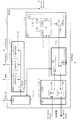
図1は、実施形態の一例としてのストレージシステムの機能構成を模式的に示す図である。
Hereinafter, in the drawings, the same reference numerals indicate the same parts, and the description thereof is omitted.
[A] Example of Embodiment [A-1] System Configuration FIG. 1 is a diagram schematically illustrating a functional configuration of a storage system as an example of an embodiment.
本実施形態の一例におけるストレージシステム100は、図1に示すように、ストレージ装置(情報処理装置)1及びサーバ装置2を備え、これらのストレージ装置1とサーバ装置2とは、例えばLocal Area Network(LAN)によって互いに通信可能に接続される。
サーバ装置2は、例えば、サーバ機能を備えたコンピュータである。図1に示す例においては、1つのサーバ装置2を備えているが、2つ以上のサーバ装置2を備えることとしても良い。
As illustrated in FIG. 1, the
The
ストレージ装置1は、後述する複数の記憶装置21を搭載し、サーバ装置2に対して記憶領域を提供する装置であり、例えばRedundant Arrays of Inexpensive Disks(RAID)を用いて複数の記憶装置21にデータを分散し、冗長化した状態で保存する。本実施形態の一例におけるストレージ装置1は、複数(図示する例では2つ)のCM10(CM#0,CM#1;制御装置)及びDisk Enclosure(DE)20を備える。
The
以下、2つのCMのうち1つを特定する必要があるときには「CM#0」又は「CM#1」と表記するが、任意のCMを指すときには「CM10」と表記する。
本ストレージ装置1は、2つのCM10を備える冗長構成とすることにより、プライマリとしてのCM10(例えばCM#0)が異常状態となった場合においてもセカンダリとしてのCM10(例えばCM#1)により継続して動作することができる。
Hereinafter, when it is necessary to specify one of the two CMs, it is expressed as “
The
DE20は、冗長化のためにCM#0,#1のそれぞれとアクセスパスで通信可能に接続されており、複数(図示する例では4つ)の記憶装置21を備える。
記憶装置21は、データを読み書き可能に格納する既知の装置であり、例えば、Hard Disk Drive(HDD)やSolid State Drive(SSD)である。これらの記憶装置21は、互いに同様の機能構成を備える。
The
The
CM10は、種々の制御を行なう制御装置であり、サーバ装置2からのストレージアクセス要求(アクセス制御信号:以下、ホストI/Oという)に従って、各種制御を行なう。本実施形態の一例におけるCM10は、FPGA11,CPU(処理装置)12,不揮発性メモリ(NVRAM,第1記憶装置,第2記憶装置)13,デバイス(監視対象装置)14,メモリ16,Input/Output Controller(IOC)17及びエキスパンダ18を備える。
The
IOC17は、CPU12とDE20との間のデータ転送を実施し、例えば、専用チップとして構成される。
エキスパンダ18は、CM10とDE20とを中継する装置であり、ホストI/Oに基づくデータ転送を行なう。すなわち、CM10は、本ストレージ装置1に備えられた各記憶装置21に対して、エキスパンダ18を介してアクセスする。
The IOC 17 performs data transfer between the
The
デバイス14は、CM10に備えられる種々の装置である。図1に示す例においては、簡単のためCM10が1つのデバイス14のみを備えているが、CM10は複数のデバイス14を備えても良い。また、デバイス14はCM10のオンボードに備えられても良いし、Peripheral Component Interconnect(PCI)カード等の種々のアドインカードをデバイス14とすることによってCM10と通信可能に接続されても良い。
The
不揮発性メモリ13は、例えばNANDフラッシュメモリやSerial Advanced Technology Attachment Solid State Drive(SATA SSD)であり、CM10への電力供給が停止してもデータを保持し続ける。本実施形態の一例において、不揮発性メモリ13は、デバイス14から採取したログ情報(システム情報)を格納する。
メモリ16は、Read Only Memory(ROM)及びRandom Access Memory(RAM)を含む記憶装置である。メモリ16のROMには、Basic Input/Output System(BIOS)等のプログラムが書き込まれている。メモリ16上のソフトウェアプログラムは、CPU12に適宜読み込まれて実行される。また、メモリ16のRAMは、例えばDouble-Data-Rate3 Synchronous Dynamic Random Access Memory(DDR3 SDRAM)であり、一次記録メモリあるいはワーキングメモリとして利用される。
The
The
CPU12は、種々の制御や演算を行なう処理装置であり、メモリ16に格納されたOperating System(OS)やプログラムを実行することにより、種々の機能を実現する。
なお、種々の機能を実現するためのプログラムは、例えばフレキシブルディスク,CD(CD−ROM,CD−R,CD−RW等),DVD(DVD−ROM,DVD−RAM,DVD−R,DVD+R,DVD−RW,DVD+RW,HD DVD等),ブルーレイディスク,磁気ディスク,光ディスク,光磁気ディスク等の、コンピュータ読取可能な記録媒体に記録された形態で提供される。そして、コンピュータはその記録媒体から図示しない読取装置を介してプログラムを読み取って内部記録装置または外部記録装置に転送し格納して用いる。又、そのプログラムを、例えば磁気ディスク,光ディスク,光磁気ディスク等の記憶装置(記録媒体)に記録しておき、その記憶装置から通信経路を介してコンピュータに提供してもよい。
The
Examples of programs for realizing various functions include flexible disks, CDs (CD-ROM, CD-R, CD-RW, etc.), DVDs (DVD-ROM, DVD-RAM, DVD-R, DVD + R, DVD). -RW, DVD + RW, HD DVD, etc.), Blu-ray disc, magnetic disc, optical disc, magneto-optical disc, etc. Then, the computer reads the program from the recording medium via a reading device (not shown), transfers the program to the internal recording device or the external recording device, and uses it. Alternatively, the program may be recorded in a storage device (recording medium) such as a magnetic disk, an optical disk, or a magneto-optical disk, and provided to the computer from the storage device via a communication path.
種々の機能を実現する際には、内部記憶装置(本実施形態ではメモリ16)に格納されたプログラムがコンピュータのマイクロプロセッサ(本実施形態ではCPU12)によって実行される。このとき、記録媒体に記録されたプログラムをコンピュータが読み取って実行してもよい。
FPGA11は、任意に構成を設定できる集積回路であり、図1に示すように、監視部111,情報採取部112,第1格納処理部113a,第2格納処理部113b,送信部114a,受信部114b及び再起動処理部115として機能する。本実施形態の一例において、CM#0のFPGA11とCM#1のFPGA11とは、例えばFPGA間通信によって通信可能に接続される。
When realizing various functions, a program stored in an internal storage device (
The
監視部111は、同一CM10上のCPU12を監視し、CPU12において発生した障害を検知する。
情報採取部112は、監視部111がCPU12における障害発生を検知した場合に、デバイス14からログ情報を採取する。
第1格納処理部113aは、情報採取部112が採取したログ情報を不揮発性メモリ13に格納する。
The monitoring unit 111 monitors the
The
The first
FPGA11(CM10)は、例えば、Non-Maskable Interrupt(NMI;処理装置強制割り込み)処理とソフトウェアリセット(ソフトリセット)処理とハードウェアリセット(ハードリセット)処理とを含む図示しない複数種類のリカバリ処理機能を備える。そして、FPGA11(CM10)は、例えば各リカバリ処理を行なう複数のタイミングにおいて、情報採取部112によるログ情報の採取と、第1格納処理部113aによるログ情報の格納とを、繰り返し行なう。つまり、不揮発性メモリ13は、各リカバリ処理に係る複数のログ情報を格納する。
The FPGA 11 (CM10) has, for example, a plurality of types of recovery processing functions (not shown) including non-maskable interrupt (NMI) processing, software reset (soft reset) processing, and hardware reset (hardware reset) processing. Prepare. Then, the FPGA 11 (CM 10) repeatedly performs collection of log information by the
送信部114aは、情報採取部112が採取したログ情報を他のCM10に送信する。例えば、CM#0の送信部114aは、情報採取部112が採取したログ情報をFPGA間通信によってCM#1に送信する。具体的には、送信部114aは、CPU12のハングアップ(動作不能状態)が確定した後に、不揮発性メモリ13に格納された複数のログ情報を送信する。なお、送信部114aによるログ情報送信処理の詳細については、図4を用いて後述する。
The
受信部114bは、他のCM10が送信したログ情報を受信する。例えば、CM#1の受信部114bは、FPGA間通信によってCM#0が送信したログ情報を受信する。
第2格納処理部113bは、受信部114bが受信したログ情報を不揮発性メモリ13に格納する。
再起動処理部115は、送信部114aがログ情報を他のCM10に送信した後に、当該再起動処理部115が備えられた(自系の)CM10を再起動させる。なお、再起動処理部115は、障害が発生した箇所(被疑箇所)及び障害が伝搬した箇所である自系のデバイス14及びCPU12のみを再起動させても良い。
The receiving
The second
The
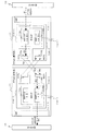
図2は、実施形態の一例としてのストレージ装置が備えるFPGAの詳細な機能構成を模式的に示す図である。
図2に示すFPGA11は、Low Pin Count bus(LPC)111−1,Watch Dog Timeout(WDT)111−2,Inter-Integrated Circuit(I2C)112,NVRAM Interface(NIF)113,Communication(COM)114−1及びProtocol Interface(PIF)114−2の各モジュールを備える。
FIG. 2 is a diagram schematically illustrating a detailed functional configuration of the FPGA included in the storage apparatus as an example of the embodiment.
2 includes a low pin count bus (LPC) 111-1, a watch dog timeout (WDT) 111-2, an inter-integrated circuit (I2C) 112, an NVRAM interface (NIF) 113, and a communication (COM) 114-. 1 and Protocol Interface (PIF) 114-2.
LPC111−1及びWDT111−2は、図1に示した監視部111としての機能に相当する。
LPC111−1は、CPU12がFPGA11にアクセスするためのインタフェース制御を行なう。
WDT111−2は、Watch Dog Timeout 1(WDTO[1])111a,WDTO[2]111b,WDTO[3]111c及びレジスタ111dの各モジュールを備える。CPU12は、LPC111−1を経由して、例えば1バイトのレジスタ111dに定期的に書き込み(ウォッチドックライト)を発行する。これにより、WDT111−2は、CPU12が正常に動作していると認識する。
The LPC 111-1 and the WDT 111-2 correspond to the function as the monitoring unit 111 illustrated in FIG.
The LPC 111-1 performs interface control for the
The WDT 111-2 includes modules of Watch Dog Timeout 1 (WDTO [1]) 111a, WDTO [2] 111b, WDTO [3] 111c, and a
WDTO[1]111aは、レジスタ111dへの書き込みが所定時間ない(ウォッチドックタイム[1]が満了した)場合に、CPU12に対してNMIを発行し、I2C112に対してログ情報採取のリクエストを発行する。
WDTO[2]111bは、レジスタ111dへの書き込みが所定時間ない(ウォッチドックタイム[2]が満了した)場合に、CPU12に対してソフトウェアリセット(ソフトリセット)の指示を発行し、I2C112に対してログ情報採取のリクエストを発行する。
The WDTO [1] 111a issues an NMI to the
The WDTO [2] 111b issues a software reset (soft reset) instruction to the
WDTO[3]111cは、レジスタ111dへの書き込みが所定時間ない(ウォッチドックタイム[3]が満了した)場合に、CPU12に対してハードウェアリセット(ハードリセット)の指示を発行し、I2C112に対してログ情報採取のリクエストを発行する。
以下、WDTO[1]111a,WDTO[2]111b及びWDTO[3]111cのリクエストによって採取されるログ情報をログ情報[1],ログ情報[2]及びログ情報[3]とそれぞれいう。
The WDTO [3] 111c issues a hardware reset (hardware reset) instruction to the
Hereinafter, log information collected by a request from WDTO [1] 111a, WDTO [2] 111b, and WDTO [3] 111c is referred to as log information [1], log information [2], and log information [3], respectively.
I2C112は、図1に示した情報採取部112としての機能に相当し、Request(REQ)112a,Finite State Machine(FSM)112b,IF112c及びレジスタ112dの各モジュールを備える。
REQ112aは、WDTO[1]111a,WDTO[2]111b又はWDTO[3]111cによるログ情報採取のリクエストをトリガとして、ログ情報採取リクエスト制御を行なう。
The
The
FSM112bは、REQ112aによるログ情報採取リクエスト制御に基づき、スイッチ15(SW;図3を用いて後述)のON/OFFの切り替えを行ない、データリードサイクルの状態管理を行なう。つまり、FSM112bは、スイッチ制御を行ない、FPGA11がI2C制御を行なうための経路を有効にする。
IF112cは、I2Cインタフェース制御を行なう。具体的には、IF112cは、1つ又は複数(図3を用いて後述する例では3つ)のデバイス14から例えば1キロバイトのログ情報[1]〜[3]をそれぞれ採取する。
Based on the log information collection request control by the
The
そして、I2C112は、IF112cを介して各デバイス14から採取したログ情報を例えば32バイトのレジスタ112dに順次格納し、格納したログ情報を例えば8バイト単位でNIF113に順次転送する。
NIF113は、図1に示した第1格納処理部113a及び第2格納処理部113bとしての機能に相当する。NIF113は、NVRAM(不揮発性メモリ)制御を行ない、REQ113−1及びIF113−2の各モジュールを備える。
The
The
REQ113−1は、NVRAM13に対する書き込み/読み出しのリクエストを受け付ける。REQ113−1が受付可能なリクエストの種類には、例えば、Write from OwnCM(I2C),Write from OtherCM(COM),Write to OtherCM(COM)及びRead from CPUがある。
Write from OwnCM(I2C)は、自系のCM10においてI2C112を介して各デバイス14から採取されたログ情報[1]〜[3]をNVRAM13に格納するリクエストである。Write from OtherCM(COM)は、他系のCM10からCOM114−1を介して受信したログ情報[1]〜[3]をNVRAM13に格納するリクエストである。Write to OtherCM(COM)は、自系のCM10において採取されたログ情報[1]〜[3]を他系のCM10に転送するリクエストである。そして、Read from CPUは、自系のCPU12からLPC111−1を介してNVRAM13が格納する種々のデータを読み出すリクエストである。
The REQ 113-1 accepts a write / read request to the
Write from OwnCM (I2C) is a request to store the log information [1] to [3] collected from each
つまり、REQ113−1がWrite from OwnCM(I2C)を受け付ける場合には、NIF113は、図1に示した第1格納処理部113aとして機能する。そして、NIF113は、I2C112からログ情報[1]〜[3]を受信すると、NVRAM13に対する書き込みを開始する。一方、REQ113−1がWrite from OtherCM(COM)を受け付ける場合には、NIF113は、図1に示した第2格納処理部113bとして機能する。そして、NIF113は、COM114−1からログ情報[1]〜[3]を受信すると、NVRAM13に対する書き込みを開始する。また、全てのログ情報[1]〜[3]についての採取及びNVRAM13に対する書き込みが完了すると、NIF113はWrite to OtherCM(COM)を受け付ける。そして、NIF113は、NVRAM13からログ情報[1]〜[3]を読み出し、他系(正常系)への送信を開始する。
That is, when the REQ 113-1 accepts Write from OwnCM (I2C), the
IF113−2は、NVRAMインタフェース制御を行なう。NIF113は、IF113−2を介してログ情報[1]〜[3]の読み書きをNVRAM13に対して行なう。
COM114−1は、他系コミュニケーション制御を行ない、Transmission Controller(TCTL)114a及びReceive Controller(RCTL)114bの各モジュールを備える。
The IF 113-2 performs NVRAM interface control. The
The COM 114-1 performs other system communication control and includes modules of a transmission controller (TCTL) 114a and a receive controller (RCTL) 114b.
TCTL114aは、図1に示した送信部114aとしての機能に相当し、トランスファ制御を行なう。具体的には、TCTL114aは、NIF113から受信したログ情報[1]〜[3]をPIF114−2を介して他系のCM10に転送する。図2に示す例において、TCTL114aは、ログ情報[1]〜[3]を送信データ(TX DATA)信号とし、クロック(CLK)信号とともに送信する。
The
RCTL114bは、図1に示した受信部114bとしての機能に相当し、レシーバ制御を行なう。具体的には、RCTL114bは、他系のCM10からPIF114−2を介して受信したログ情報[1]〜[3]をNIF113に転送する。図2に示す例において、RCTL114bは、ログ情報[1]〜[3]を含む受信データ(RX DATA)信号をクロック(CLK)信号とともに受信する。
The
PIF114−2は、他系通信プロトコルインタフェース制御を行なう。他系通信プロトコルインタフェース制御で用いられるパケットについては、図5及び図6を用いて後述する。
そして、FPGA11は、図1に示した再起動処理部115としての機能に相当するモジュール(不図示)を備える。当該モジュールは、他系(正常系)へのログ情報[1]〜[3]の送信が完了すると、自系のCM10を再起動させる。
The PIF 114-2 performs other system communication protocol interface control. Packets used in other-system communication protocol interface control will be described later with reference to FIGS.
The
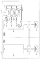
図3は、実施形態の一例としてのストレージ装置が備えるCMにおけるログ情報収集処理を例示する図である。
図3においては、本実施形態の一例としてのストレージ装置1が備えるCM#0及びCM#1を例示している。また、図3に示す例においては、CM#0を異常系とし、CM#1を正常系とする。
FIG. 3 is a diagram illustrating log information collection processing in a CM included in the storage apparatus as an example of the embodiment.
FIG. 3 illustrates
図3においては、簡単のため、CM#1が備えるデバイス14,メモリ16,IOC17及びエキスパンダ18の図示を省略している。また、CM#1が備えるメモリ16,IOC17及びエキスパンダ18の図示も省略し、CM#1は3つのデバイス(デバイス#0〜#2,監視対象装置)14及びスイッチ(SW)15を備えることとしている。
以下、3つのデバイスのうち1つを特定する必要があるときには「デバイス#0」,「デバイス#1」又は「デバイス#2」と表記するが、任意のデバイスを指すときには「デバイス14」と表記する。
In FIG. 3, for simplicity, illustration of the
Hereinafter, when it is necessary to specify one of the three devices, it is expressed as “
CM#0のFPGA11とCM#1のFPGA11とは、FPGA間通信により互いに通信可能に接続される。また、各CM10において、FPGA11とCPU12とは例えばバス線を介して互いに通信可能に接続され、FPGA11と不揮発性メモリ13とも例えばバス線を介して互いに通信可能に接続される。
CM#0においては、CPU12は、Peripheral Component Interconnect Express(PCIe)やSerial Attached Small computer system interface(SAS)等の3つの高速IF121及び低速IF122を備える。また、各デバイス14は、高速IF141及び低速IF142を備える。そして、CPU12の各高速IF121と各デバイス14の高速IF141とは、データ通信用高速バスによって互いに通信可能に接続される。また、CPU12の低速IF122と各デバイス14の低速IF142とは、SW15を介して、ログ採取用低速バスによって互いに通信可能に接続される。更に、FPGA11と各デバイス14の低速IF142とも、SW15を介して、ログ採取用低速バスによって互いに通信可能に接続される。
The
In
図3に示す例においては、CM#0のCPU12の高速IF121とデバイス#0の高速IF141との間のデータ通信用高速バスで障害が発生している(符号A1参照)。そして、発生した障害がCPU12に伝搬し、CPU12がハングアップ状態になっている(符号A2参照)。このように、CPU12がハングアップ状態になった場合には、CPU12によるログ採取用低速バスを用いたログ情報収集処理が実行できなくなり、デバイス14からログ情報を採取できない。
In the example shown in FIG. 3, a failure has occurred in the high-speed bus for data communication between the high-speed IF 121 of the
そこで、本実施形態の一例においては、CPU12におけるハングアップが発生した場合に、ハードウェアであるFPGA11がログ情報の採取を自動実行し、採取したログ情報を正常系のCM#1に送信する。
具体的には、FPGA11は、CPU12における異常発生を検知し、CPU12と各デバイス14とをログ採取用低速バスで接続しているSW15の経路をFPGA11と各デバイス14とが接続されるように切り替える(符号A3参照)。言い換えれば、FPGA11は、図2を用いて説明したウォッチドックタイム[1]〜[3]のいずれかが満了した場合に、SW15を操作してCPU12をログ採取用低速バスから切断する。
Therefore, in an example of the present embodiment, when the
Specifically, the
FPGA11は、各デバイス14からログ情報を採取し(符号A4参照)、採取したログ情報を不揮発性メモリ13に格納する(符号A5参照)。言い換えれば、FPGA11は、ログ情報採取処理においてマスターとなり、ログ採取用低速バスを介してスレーブとしてのデバイス14にアクセスすることにより、デバイス14からログ情報を採取する。
ここで、CM#0のCPU12においては異常が発生しているため、FPGA11によって採取されたログ情報を異常系のCM#0で直ちに解析することはできない。そこで、FPGA11は、ウォッチドックタイムアウトから復帰した(CPU12の正常作動を認識した)場合や、CPU12のハングアップが確定した場合に、採取したログ情報を不揮発性メモリ13から読み出す。そして、FPGA11は、不揮発性メモリ13から読み出したログ情報を正常起動している他系のCM#1にFPGA間通信を用いて送信する(符号A6参照)。
The
Here, since an abnormality has occurred in the
正常系のCM#1のFPGA11は、異常系のCM#0から送信されたログ情報を受信し、不揮発性メモリ13に格納し(符号A7参照)、ログ情報の受信完了を自系のCPU12に通知する。
CM#1のCPU12は、FPGA11を介して自系の不揮発性メモリ13からログ情報を読み出し(符号A8参照)、読み出したログ情報を装置ログとして例えばメモリ16(図3には不図示)に格納する。
The
The
図4は、実施形態の一例としてのストレージ装置におけるログ情報送受信処理を説明する図である。
図4においては、本実施形態の一例としてのストレージ装置1が備えるCM#0及びCM#1の機能構成のうち一部を例示している。具体的には、図1に示した各CM10が備える機能構成のうち、FPGA11及び不揮発性メモリ(NVRAM)13のみを示している。また、各CM10のFPGA11においては、図2に示したFPGA11が備える機能構成のうち、NIF113及びCOM114−1のみを示している。
FIG. 4 is a diagram illustrating log information transmission / reception processing in the storage apparatus as an example of the embodiment.
FIG. 4 illustrates a part of the functional configurations of
図4に示す例においては、COM114−1は、図2に示したTCTL114a及びRCTL114bに加えて、バッファ(BUF)[0]114c及びBUF[1]114dを備える。言い換えれば、COM114−1の一部は、図4に示すように、Block Buffer(BBUF)として機能する。
異常系のFPGA11のNIF113は、Write to OtherCM(COM)を受け付けると、NVRAM13からログ情報を読み出し、COM114−1のBUF[0]114cに格納する(符号B1参照)。NVRAM13から読み出されるログ情報は、例えば、データ(DT)が8ビット(1バイト)であり、アドレス(AD)が24ビット(3バイト)である。
In the example illustrated in FIG. 4, the COM 114-1 includes a buffer (BUF) [0] 114 c and a BUF [1] 114 d in addition to the
When receiving the Write to Other CM (COM), the
BUF[0]114cは、格納したログ情報をTCTL114aに転送する(符号B2参照)。
TCTL114aは、ログ情報を図5及び図6を用いて後述するパケットとして正常系のFPGA11宛てに送信する(符号B3)。TCTL114aは、TX_DATAとしてパケットを送信し、TX_CLKとしてクロック信号を送信する。
The BUF [0] 114c transfers the stored log information to the
The
正常系のFPGA11のRCTL114bは、異常系のFPGA11が送信したパケットを受信し、ログ情報としてBUF[1]114dに格納する(符号B4参照)。RCTL114bは、RX_DATAとしてパケットを受信し、RX_CLKとしてクロック信号を受信する。
BUF[1]114dは格納したログ情報をNIF113に転送し、NIF113はWrite from OtherCM(COM)を受け付けることによってログ情報をNVRAM13に格納する(符号B5参照)。NVRAM13に書き込まれるログ情報は、例えば、データ(DT)が8ビット(1バイト)であり、アドレス(AD)が24ビット(3バイト)である。
The
The BUF [1] 114d transfers the stored log information to the
図5及び図6は、実施形態の一例としてのストレージ装置が使用するパケットを例示する図である。
本実施形態の一例におけるログ情報送受信処理に用いるパケットは、図5に示すように、64ビット(8バイト)で定義される。具体的には、63〜60ビットがStart Of Frame(SOF)であり、59〜52ビットがPacket ID(PID)であり、51〜44ビットがSerial ID(SID)であり、43〜12ビットがPayload(送信データ)であり、11〜4ビットが Cyclic Redundancy Check(CRC;保護コード)であり、3〜0ビットがEnd Of Frame(EOF)である。
5 and 6 are diagrams illustrating packets used by the storage apparatus as an example of the embodiment.
A packet used for log information transmission / reception processing in an example of this embodiment is defined by 64 bits (8 bytes) as shown in FIG. Specifically, 63 to 60 bits are Start Of Frame (SOF), 59 to 52 bits are Packet ID (PID), 51 to 44 bits are Serial ID (SID), and 43 to 12 bits are Payload (transmission data), 11 to 4 bits are Cyclic Redundancy Check (CRC; protection code), and 3 to 0 bits are End Of Frame (EOF).
図5に示すように、SOFには“1111”が設定される。また、図5に示すようにPIDの59〜56ビットにはそれぞれ“0”が設定され、図6に示すようにPIDの55〜52ビットには“00”〜“0c”が設定される。更に、図6に示すように、SIDには“0x00”〜“0xFF”が設定される。
図5に示すように、Payloadは領域(4)〜(1)に分割され、領域(4)〜(1)はPayloadにおける31〜24,23〜16,15〜8及び7〜0ビットにそれぞれ対応する。そして、図6に示すように、PIDが“00”〜“03”の場合には、Payloadの領域(4)にログ情報[1]に関する1キロバイトのデータが格納される。また、PIDが“04”〜“07”の場合にはPayloadの領域(4)にログ情報[2]に関する1キロバイトのデータが格納され、PIDが“08”〜“0C”の場合にはPayloadの領域(4)にログ情報[3]に関する1キロバイトのデータが格納される。更に、Payloadの領域(3)は拡張(Reserve)領域であり、Payloadの領域(2)及び(1)にはNVRAM13におけるアドレスが設定される。
As shown in FIG. 5, “1111” is set in the SOF. Further, as shown in FIG. 5, “0” is set to 59 to 56 bits of PID, and “00” to “0c” is set to 55 to 52 bits of PID as shown in FIG. Furthermore, as shown in FIG. 6, “0x00” to “0xFF” are set in the SID.
As shown in FIG. 5, Payload is divided into areas (4) to (1), and areas (4) to (1) are respectively divided into 31-24, 23-16, 15-8 and 7-0 bits in Payload. Correspond. As shown in FIG. 6, when the PID is “00” to “03”, 1 kilobyte data relating to the log information [1] is stored in the Payload area (4). When the PID is “04” to “07”, 1 kilobyte data relating to the log information [2] is stored in the Payload area (4), and when the PID is “08” to “0C”, the Payload is stored. In the area (4), 1 kilobyte data relating to the log information [3] is stored. Further, the Payload area (3) is an extension (Reserve) area, and addresses in the
図5に示す6つの両矢印はCRC演算単位であり、各CRC演算単位におけるCRC演算結果がCRCに設定される。そして、図5に示すように、EOFには“0000”が設定される。
なお、本実施形態の一例におけるログ情報送受信処理に用いるパケットの転送性能は、図6に示すように、1.0msである。
The six double arrows shown in FIG. 5 are CRC calculation units, and the CRC calculation result in each CRC calculation unit is set to CRC. As shown in FIG. 5, “0000” is set in the EOF.
Note that the transfer performance of the packet used for the log information transmission / reception process in the example of this embodiment is 1.0 ms as shown in FIG.
〔A−2〕動作
上述の如く構成された実施形態の一例としてのストレージ装置におけるログ情報収集処理を図7に示すフローチャート(ステップS1〜S16)に従って説明する。
WDT111−2は、CPU12からレジスタ111dに対する定期的な書き込みを検知するできないことにより、CPU12における障害発生を検知する(ステップS1)。
[A-2] Operation Log information collection processing in the storage apparatus as an example of the embodiment configured as described above will be described with reference to the flowchart (steps S1 to S16) shown in FIG.
The WDT 111-2 detects the occurrence of a failure in the
WDTO[1]111aは、ウォッチドックタイム[1]をカウントする(ステップS2)。
CPU12からレジスタ111dに対する書き込みが所定時間(例えば5秒)以内にあった場合には(ステップS2の“カウントクリア”ルート参照)、ウォッチドックタイム[1]のカウントをクリアしてステップS2に戻る。つまり、ウォッチドックタイム[1]のカウントを繰り返し行なう。
The WDTO [1] 111a counts the watchdog time [1] (step S2).
If writing to the
一方、CPU12からレジスタ111dに対する書き込みがない状態で所定時間(例えば5秒)経過した場合には(ステップS2の“5秒”ルート参照)、WDTO[1]111aは、CPU12に対してNMIを発行する(ステップS3)。
I2C112は、各デバイス14(例えば図3に示したデバイス#0〜#2)からのログ情報[1]の採取(ダンプ[1])を開始する(ステップS4)。
On the other hand, when a predetermined time (for example, 5 seconds) has elapsed without writing to the
The
CPU12は、リカバリを実行する(ステップS5)。
リカバリによってCPU12が復帰した場合には(ステップS5の“復帰”ルート参照)、TCTL114aはFPGA間通信によって採取したログ情報[1]を他系のFPGA11に送信するとともに(ステップS15)、ステップS1に戻り待機する。
一方、リカバリに失敗した場合には(ステップS5の“リカバリ失敗”ルート参照)、WDTO[2]111bは、ウォッチドックタイム[2]をカウントする(ステップS6)。
The
When the
On the other hand, when recovery fails (see the “recovery failure” route in step S5), the WDTO [2] 111b counts the watchdog time [2] (step S6).
CPU12からレジスタ111dに対する書き込みが所定時間(例えば5秒)以内にあった場合には(ステップS6の“カウントクリア”ルート参照)、ウォッチドックタイム[2]のカウントをクリアしてステップS6に戻る。つまり、ウォッチドックタイム[2]のカウントを再開する。
一方、CPU12からレジスタ111dに対する書き込みがない状態で所定時間(例えば5秒)経過した場合には(ステップS6の“5秒”ルート参照)、WDTO[2]111bは、CPU12に対してソフトウェアリセットの指示を発行する(ステップS7)。
If writing to the
On the other hand, when a predetermined time (for example, 5 seconds) elapses without writing to the
I2C112は、各デバイス14(例えば図3に示したデバイス#0〜#2)からのログ情報[2]の採取(ダンプ[2])を開始する(ステップS8)。
CPU12は、リカバリを実行する(ステップS9)。
リカバリによってCPU12が復帰した場合には(ステップS9の“復帰”ルート参照)、TCTL114aはFPGA間通信によって採取したログ情報[1]及び[2]を他系のFPGA11に送信するとともに(ステップS15)、ステップS1に戻り待機する。
The
The
When the
一方、リカバリに失敗した場合には(ステップS9の“リカバリ失敗”ルート参照)、WDTO[3]111cは、ウォッチドックタイム[3]をカウントする(ステップS10)。
CPU12からレジスタ111dに対する書き込みが所定時間(例えば10秒)以内にあった場合には(ステップS10の“カウントクリア”ルート参照)、ウォッチドックタイム[3]のカウントをクリアしてステップS10に戻る。つまり、ウォッチドックタイム[3]のカウントを再開する。
On the other hand, when the recovery fails (see the “recovery failure” route in step S9), the WDTO [3] 111c counts the watchdog time [3] (step S10).
If writing to the
一方、CPU12からレジスタ111dに対する書き込みがない状態で所定時間(例えば10秒)経過した場合には(ステップS10の“10秒”ルート参照)、WDTO[3]111cは、CPU12に対してハードウェアリセットの指示を発行する(ステップS11)。
I2C112は、各デバイス14(例えば図3に示したデバイス#0〜#2)からのログ情報[3]の採取(ダンプ[3])を開始する(ステップS12)。
On the other hand, when a predetermined time (for example, 10 seconds) has elapsed without writing to the
The
CPU12は、リカバリを実行する(ステップS13)。
リカバリによってCPU12が復帰した場合には(ステップS13の“復帰”ルート参照)、TCTL114aはFPGA間通信によって採取したログ情報[1],[2]及び[3]を他系のFPGA11に送信するとともに(ステップS15)、ステップS1に戻り待機する。
The
When the
一方、リカバリに失敗した場合には(ステップS13の“リカバリ失敗”ルート参照)、FPGA11は、CPU12のハングアップが確定したと判断する(ステップS14)。
そして、TCTL114aは採取したログ情報[1],[2]及び[3]をFPGA間通信によって他系のFPGA11に送信するとともに(ステップS15)、FPGA11はファームウェア処理によって自系のCM10をDC−OFF状態にする(ステップS16)。つまり、FPGA11は、自系のCM10を再起動する。なお、FPGA11は、障害が発生した箇所(被疑箇所)及び障害が伝搬した箇所である自系のデバイス14及びCPU12のみを再起動させても良い。
On the other hand, when the recovery fails (see the “recovery failure” route in step S13), the
The
次に、上述の如く構成された実施形態の一例としてのストレージ装置におけるログ情報収集処理を図8に例示するシーケンス図(ステップS21〜S51)に従って説明する。
図8に示すCM#0及びCM#1は図3に示したCM#0及びCM#1とそれぞれ同様の機能構成を備え、CM#0が異常系であり、CM#1が正常系である。
CM#0のCPU12は、FPGA11に対して定期的にウォッチドックライトを行なう。FPGA11のWDTO[1]111a,WDTO[2]111b及びWDTO[3]111cは、CPU12からのウォッチドックライトによりCPU12が正常に作動しているとそれぞれ認識する(ステップS21〜S23)。
Next, log information collection processing in the storage apparatus as an example of the embodiment configured as described above will be described with reference to a sequence diagram (steps S21 to S51) illustrated in FIG.
The
ここで、デバイス#1において異常が発生し(ステップS24)、発生した異常がCPU12に伝搬する(ステップS25)。
FPGA11のWDTO[1]111aは、ウォッチドックタイム[1]の満了により、CPU12に対してNMIを発行する(ステップS26)。
FPGA11のI2C112は、SW15を切り替えることにより、FPGA11と各デバイス14との経路をONにする(ステップS27)。
Here, an abnormality occurs in the device # 1 (step S24), and the generated abnormality propagates to the CPU 12 (step S25).
The WDTO [1] 111a of the
The
FPGA11のI2C112は、デバイス#0〜#2からログ情報[1]を採取する(ステップS28〜S30)。
FPGA11のNIF113は、採取したログ情報[1]をNVRAM13に格納する(ステップS31)。
FPGA11のI2C112は、SW15を切り替えることにより、FPGA11と各デバイス14との経路をOFFにする(ステップS32)。
The
The
The
FPGA11のWDTO[2]111bは、ウォッチドックタイム[2]の満了により、CPU12に対してソフトウェアリセットを指示する(ステップS33)。
FPGA11のI2C112は、SW15を切り替えることにより、FPGA11と各デバイス14との経路をONにする(ステップS34)。
FPGA11のI2C112は、デバイス#0〜#2からログ情報[2]を採取する(ステップS35〜S37)。
When the watchdog time [2] expires, the WDTO [2] 111b of the
The
The
FPGA11のNIF113は、採取したログ情報[2]をNVRAM13に格納する(ステップS38)。
FPGA11のI2C112は、SW15を切り替えることにより、FPGA11と各デバイス14との経路をOFFにする(ステップS39)。
FPGA11のWDTO[3]111bは、ウォッチドックタイム[3]の満了により、CPU12に対してハードウェアリセットを指示する(ステップS40)。
The
The
The WDTO [3] 111b of the
FPGA11のI2C112は、SW15を切り替えることにより、FPGA11と各デバイス14との経路をONにする(ステップS41)。
FPGA11のI2C112は、デバイス#0〜#2からログ情報[3]を採取する(ステップS42〜S44)。
FPGA11のNIF113は、採取したログ情報[3]をNVRAM13に格納する(ステップS45)。
The
The
The
FPGA11のI2C112は、SW15を切り替えることにより、FPGA11と各デバイス14との経路をOFFにする(ステップS46)。
FPGA11は、CPU12のハングアップが確定したと判断する(ステップS47)。
FPGA11のTCTL114aは、採取したログ情報[1],[2]及び[3]をNVRAM13から読み出し、正常系であるCM#1のFPGA11に送信する(ステップS48)。
The
The
The
CM#1のFPGA11は、受信したログ情報[1],[2]及び[3]をNVRAM13に格納する(ステップS49)。
CM#0のFPGA11は、自系のCM#0を再起動する(ステップS50)。なお、FPGA11は、障害が発生した箇所(被疑箇所)及び障害が伝搬した箇所である自系のデバイス14及びCPU12のみを再起動させても良い。
The
The
CM#1のCPU12は、NVRAM13からエラーログを採取する(ステップS51)。
〔A−3〕効果
このように、本実施形態の一例におけるストレージ装置(情報処理装置)1によれば、以下の効果を奏することができる。
The
[A-3] Effects As described above, according to the storage apparatus (information processing apparatus) 1 in the example of the present embodiment, the following effects can be obtained.
情報採取部112は、監視部111が処理装置12における障害発生を検知した場合に、監視対象装置14からログ情報を採取する。そして、第1格納処理部113aは、情報採取部112が採取したログ情報を記憶装置13に格納する。これにより、処理装置12の動作不能状態においても監視対象装置14のログ情報の収集を確実に行なうことができる。また、制御装置10における障害復旧後や記憶装置13の取り外し後に、記憶装置13に格納されたログ情報が解析することができる。
The
送信部114aは、情報採取部112が採取したログ情報を他の制御装置10に送信する。そして、他の制御装置10の第2格納処理部113bは、送信部114aが送信したログ情報を記憶装置13に格納する。これにより、正常系の制御装置10においてログ情報の解析を直ちに開始することができる。また、異常系の制御装置10について、障害発生の被疑箇所を特定するために、異常系の制御装置10を回収し、測定機器に取り付け、処理装置12の動作不能状態を再現させ、手動でログ情報を採取する必要がない。つまり、被疑箇所の特定に要する工数や時間,コストを削減することができ、被疑箇所の特定が容易になる。更に、異常系及び正常系の制御装置10の記憶装置13にログ情報が二重化されて格納されるため、ログ情報収集処理における信頼性を向上することができる。
The
再起動処理部115は、送信部114aがログ情報を他の制御装置10に送信した後に、処理装置12及び監視対象装置14を再起動させる。これにより、異常系の制御装置10における再起動によって記憶装置13に格納したログ情報が消失した場合においても、正常系の制御装置10においてログ情報を解析することができる。
処理装置強制割り込み処理とソフトウェアリセット処理とハードウェアリセット処理とを実行する複数のタイミングにおいて、情報採取部112によるログ情報の採取と、第1格納処理部113aによるログ情報の格納とを、繰り返し行なう。これにより、各リカバリ処理後における監視対象装置14の状態を示すログ情報[1]〜[3]を採取することができ、被疑箇所の特定が容易になる。
The
Collection of log information by the
〔B〕変形例
開示の技術は上述した実施形態に限定されるものではなく、本実施形態の趣旨を逸脱しない範囲で種々変形して実施することができる。本実施形態の各構成及び各処理は、必要に応じて取捨選択することができ、あるいは適宜組み合わせてもよい。
上述した実施形態の一例においては、異常系のFPGA11は、全てのログ情報[1]〜[3]をNVRAM13に格納した後に、ログ情報[1]〜[3]を正常系のFPGA11に転送することとしたが(例えば図8のステップS48参照)、これに限定されるものではない。
[B] Modified Examples The disclosed technique is not limited to the above-described embodiment, and various modifications can be made without departing from the spirit of the present embodiment. Each structure and each process of this embodiment can be selected as needed, or may be combined suitably.
In the example of the embodiment described above, the
本実施形態の変形例においては、異常系のFPGA11は、各ログ情報[1]〜[3]をNVRAM13に格納した直後(例えば、図8のステップS31,S38及びS45の直後)に、各ログ情報[1]〜[3]を正常系のFPGA11に逐次転送する。
そして、異常系のFPGA11は、CPU12のハングアップが確定した後(例えば図8のステップS47の後)に、全てのログ情報[1]〜[3]の転送が完了したことを示す完了通知を正常系のFPGA11に送信する。
In the modification of the present embodiment, the
Then, after confirming that the
このように、本実施形態の変形例におけるストレージ装置(情報処理装置)1によっても、上述した実施形態の一例と同様の効果を奏することができる他、以下の効果を奏することができる。
各ログ情報[1]〜[3]を上述した実施形態の一例における場合よりも早く正常系のCM10に送信することができ、正常系のCM10は、ログ情報の解析を早期に開始することができ、他系のCM10で異常が発生したことを示すアラート等を迅速に発行することができる。
As described above, the storage apparatus (information processing apparatus) 1 according to the modification of the present embodiment can achieve the same effects as the above-described example of the embodiment and the following effects.
Each log information [1] to [3] can be transmitted to the
〔C〕付記
(付記1)
監視対象装置と通信可能に接続される制御装置を有する情報処理装置であって、
前記制御装置は、
処理装置における障害発生を監視する監視部と、
前記監視部が前記障害発生を検知した場合に、前記監視対象装置からログ情報を採取する情報採取部と、
前記情報採取部が採取した前記ログ情報を第1記憶装置に格納する第1格納処理部と、
を備えることを特徴とする、情報処理装置。
[C] Appendix (Appendix 1)
An information processing apparatus having a control device communicably connected to a monitoring target device,
The controller is
A monitoring unit for monitoring the occurrence of a failure in the processing device;
An information collecting unit for collecting log information from the monitoring target device when the monitoring unit detects the occurrence of the failure;
A first storage processing unit for storing the log information collected by the information collecting unit in a first storage device;
An information processing apparatus comprising:
(付記2)
当該情報処理装置は、複数の制御装置を備え、
前記制御装置は、前記情報採取部が採取した前記ログ情報を前記複数の制御装置のうち他の制御装置に送信する送信部
を備え、
前記他の制御装置は、前記送信部が送信した前記ログ情報を第2記憶装置に格納する第2格納処理部
を備えることを特徴とする、付記1に記載の情報処理装置。
(Appendix 2)
The information processing apparatus includes a plurality of control devices,
The control device includes a transmission unit that transmits the log information collected by the information collection unit to another control device among the plurality of control devices,
The information processing apparatus according to
(付記3)
前記送信部は、前記処理装置の動作不能状態が確定した後に、前記ログ情報を前記他の制御装置に送信する、
ことを特徴とする、付記2に記載の情報処理装置。
(付記4)
前記制御装置は、
前記送信部が前記ログ情報を前記他の制御装置に送信した後に、前記処理装置及び前記監視対象装置を再起動させる再起動処理部
を備えることを特徴とする、付記2又は3に記載の情報処理装置。
(Appendix 3)
The transmission unit transmits the log information to the other control device after the inoperable state of the processing device is determined.
The information processing apparatus according to
(Appendix 4)
The controller is
The information according to
(付記5)
前記制御装置は、
複数のタイミングにおいて、前記情報採取部による前記ログ情報の採取と、前記第1格納処理部による前記ログ情報の格納とを、繰り返し行なう、
ことを特徴とする、付記1〜4のいずれか1項に記載の情報処理装置。
(Appendix 5)
The controller is
In a plurality of timings, the collection of the log information by the information collection unit and the storage of the log information by the first storage processing unit are repeatedly performed.
The information processing apparatus according to any one of
(付記6)
前記制御装置は、
処理装置強制割り込み処理とソフトウェアリセット処理とハードウェアリセット処理とを含む複数種類のリカバリ処理機能を備え、
各リカバリ処理を行なうタイミングを前記複数のタイミングとする、
ことを特徴とする、付記5に記載の情報処理装置。
(Appendix 6)
The controller is
With multiple types of recovery processing functions including processing device forced interrupt processing, software reset processing, and hardware reset processing,
The timing of performing each recovery process is the plurality of timings,
The information processing apparatus according to appendix 5, wherein:
(付記7)
監視対象装置と通信可能に接続される制御装置であって、
処理装置における障害発生を監視する監視部と、
前記監視部が前記障害発生を検知した場合に、前記監視対象装置からログ情報を採取する情報採取部と、
前記情報採取部が採取した前記ログ情報を第1記憶装置に格納する第1格納処理部と、
を備えることを特徴とする、制御装置。
(Appendix 7)
A control device communicably connected to the monitored device,
A monitoring unit for monitoring the occurrence of a failure in the processing device;
An information collecting unit for collecting log information from the monitoring target device when the monitoring unit detects the occurrence of the failure;
A first storage processing unit for storing the log information collected by the information collecting unit in a first storage device;
A control device comprising:
(付記8)
前記情報採取部が採取した前記ログ情報を当該制御装置と通信可能に接続される他の制御装置に送信する送信部
を備えることを特徴とする、付記7に記載の制御装置。
(付記9)
前記送信部は、前記処理装置の動作不能状態が確定した後に、前記ログ情報を前記他の制御装置に送信する、
ことを特徴とする、付記8に記載の制御装置。
(Appendix 8)
The control apparatus according to
(Appendix 9)
The transmission unit transmits the log information to the other control device after the inoperable state of the processing device is determined.
9. The control device according to
(付記10)
前記送信部が前記ログ情報を前記他の制御装置に送信した後に、前記処理装置及び前記監視対象装置を再起動させる再起動処理部
を備えることを特徴とする、付記8又は9に記載の制御装置。
(付記11)
複数のタイミングにおいて、前記情報採取部による前記ログ情報の採取と、前記第1格納処理部による前記ログ情報の格納とを、繰り返し行なう、
ことを特徴とする、付記7〜10のいずれか1項に記載の制御装置。
(Appendix 10)
The control according to
(Appendix 11)
In a plurality of timings, the collection of the log information by the information collection unit and the storage of the log information by the first storage processing unit are repeatedly performed.
The control device according to any one of
(付記12)
処理装置強制割り込み処理とソフトウェアリセット処理とハードウェアリセット処理とを含む複数種類のリカバリ処理機能を備え、
各リカバリ処理を行なうタイミングを前記複数のタイミングとする、
ことを特徴とする、付記11に記載の制御装置。
(Appendix 12)
With multiple types of recovery processing functions including processing device forced interrupt processing, software reset processing, and hardware reset processing,
The timing of performing each recovery process is the plurality of timings,
The control apparatus according to
(付記13)
監視対象装置と通信可能に接続される制御装置を有する情報処理装置におけるログ情報収集方法であって、
前記制御装置は、
処理装置における障害発生を監視し、
前記障害発生を検知した場合に、前記監視対象装置からログ情報を採取し、
採取した前記ログ情報を第1記憶装置に格納する、
ことを特徴とする、ログ情報収集方法。
(Appendix 13)
A log information collecting method in an information processing apparatus having a control device communicably connected to a monitoring target device,
The controller is
Monitor faults in processing equipment,
When the failure occurrence is detected, log information is collected from the monitored device,
Storing the collected log information in a first storage device;
A method for collecting log information.
(付記14)
当該情報処理装置は、複数の制御装置を備え、
前記制御装置は、採取した前記ログ情報を前記複数の制御装置のうち他の制御装置に送信し、
前記他の制御装置は、前記制御装置から送信された前記ログ情報を第2記憶装置に格納する、
ことを特徴とする、付記13に記載のログ情報収集方法。
(Appendix 14)
The information processing apparatus includes a plurality of control devices,
The control device transmits the collected log information to another control device among the plurality of control devices,
The other control device stores the log information transmitted from the control device in a second storage device.
14. The log information collecting method according to
(付記15)
前記制御装置は、
前記処理装置の動作不能状態が確定した後に、前記ログ情報を前記他の制御装置に送信する、
ことを特徴とする、付記14に記載のログ情報収集方法。
(Appendix 15)
The controller is
After the inoperable state of the processing device is determined, the log information is transmitted to the other control device.
15. The log information collection method according to
(付記16)
前記制御装置は、
前記ログ情報を前記他の制御装置に送信した後に、前記処理装置及び前記監視対象装置を再起動させる、
ことを特徴とする、付記14又は15に記載のログ情報収集方法。
(Appendix 16)
The controller is
After transmitting the log information to the other control device, restart the processing device and the monitoring target device,
The log information collection method according to
(付記17)
前記制御装置は、
複数のタイミングにおいて、前記ログ情報の採取と、前記ログ情報の格納とを、繰り返し行なう、
ことを特徴とする、付記13〜16のいずれか1項に記載のログ情報収集方法。
(Appendix 17)
The controller is
In a plurality of timings, the collection of the log information and the storage of the log information are repeated.
The log information collection method according to any one of
(付記18)
前記制御装置は、
処理装置強制割り込み処理とソフトウェアリセット処理とハードウェアリセット処理とを含む複数種類のリカバリ処理機能を備え、
各リカバリ処理を行なうタイミングを前記複数のタイミングとする、
ことを特徴とする、付記17に記載のログ情報収集方法。
(Appendix 18)
The controller is
With multiple types of recovery processing functions including processing device forced interrupt processing, software reset processing, and hardware reset processing,
The timing of performing each recovery process is the plurality of timings,
18. The log information collection method according to
100 ストレージシステム
1 ストレージ装置(情報処理装置)
10 CM(制御装置)
11 FPGA
111 監視部
111−1 LPC
111−2 WDT
111a WDTO[1]
111b WDTO[2]
111c WDTO[3]
111d レジスタ
112 情報採取部(I2C)
112a REQ
112b FSM
112c IF
112d レジスタ
113 NIF
113a 第1格納処理部
113b 第2格納処理部
113−1 REQ
113−2 IF
114−1 COM
114a 送信部(TCTL)
114b 受信部(RCTL)
114c BUF[0]
114d BUF[1]
114−2 PIF
12 CPU(処理装置)
121 高速IF
122 低速IF
13 不揮発性メモリ(NVRAM;第1記憶装置,第2記憶装置)
14 デバイス(監視対象装置)
141 高速IF
142 低速IF
15 SW
16 メモリ
17 IOC
18 エキスパンダ
20 DE
21 記憶装置
2 サーバ装置
30 CM
31 FPGA
32 CPU
321 高速IF
322 低速IF
33 不揮発性メモリ
34 デバイス
341 高速IF
342 低速IF
35 SW
100
10 CM (control device)
11 FPGA
111 monitoring unit 111-1 LPC
111-2 WDT
111a WDTO [1]
111b WDTO [2]
111c WDTO [3]
111d register 112 information collecting unit (I2C)
112a REQ
112b FSM
112c IF
112d register 113 NIF
113a First
113-2 IF
114-1 COM
114a Transmitter (TCTL)
114b Receiver (RCTL)
114c BUF [0]
114d BUF [1]
114-2 PIF
12 CPU (Processor)
121 High-speed IF
122 Low speed IF
13 Nonvolatile memory (NVRAM; first storage device, second storage device)
14 devices (monitored devices)
141 High-speed IF
142 Low speed IF
15 SW
16
18
21
31 FPGA
32 CPU
321 High-speed IF
322 Low speed IF
33
342 Low speed IF
35 SW
Claims (8)
前記制御装置は、
処理装置における障害発生を監視する監視部と、
前記監視部が前記障害発生を検知した場合に、前記監視対象装置からログ情報を採取する情報採取部と、
前記情報採取部が採取した前記ログ情報を第1記憶装置に格納する第1格納処理部と、
を備えることを特徴とする、情報処理装置。 An information processing apparatus having a control device communicably connected to a monitoring target device,
The controller is
A monitoring unit for monitoring the occurrence of a failure in the processing device;
An information collecting unit for collecting log information from the monitoring target device when the monitoring unit detects the occurrence of the failure;
A first storage processing unit for storing the log information collected by the information collecting unit in a first storage device;
An information processing apparatus comprising:
前記制御装置は、前記情報採取部が採取した前記ログ情報を前記複数の制御装置のうち他の制御装置に送信する送信部
を備え、
前記他の制御装置は、前記送信部が送信した前記ログ情報を第2記憶装置に格納する第2格納処理部
を備えることを特徴とする、請求項1に記載の情報処理装置。 The information processing apparatus includes a plurality of control devices,
The control device includes a transmission unit that transmits the log information collected by the information collection unit to another control device among the plurality of control devices,
The information processing apparatus according to claim 1, wherein the other control apparatus includes a second storage processing unit that stores the log information transmitted by the transmission unit in a second storage device.
ことを特徴とする、請求項2に記載の情報処理装置。 The transmission unit transmits the log information to the other control device after the inoperable state of the processing device is determined.
The information processing apparatus according to claim 2, wherein:
前記送信部が前記ログ情報を前記他の制御装置に送信した後に、前記処理装置及び前記監視対象装置を再起動させる再起動処理部
を備えることを特徴とする、請求項2又は3に記載の情報処理装置。 The controller is
4. The apparatus according to claim 2, further comprising a restart processing unit configured to restart the processing device and the monitoring target device after the transmitting unit transmits the log information to the other control device. 5. Information processing device.
複数のタイミングにおいて、前記情報採取部による前記ログ情報の採取と、前記第1格納処理部による前記ログ情報の格納とを、繰り返し行なう、
ことを特徴とする、請求項1〜4のいずれか1項に記載の情報処理装置。 The controller is
In a plurality of timings, the collection of the log information by the information collection unit and the storage of the log information by the first storage processing unit are repeatedly performed.
The information processing apparatus according to any one of claims 1 to 4, wherein the information processing apparatus is characterized.
処理装置強制割り込み処理とソフトウェアリセット処理とハードウェアリセット処理とを含む複数種類のリカバリ処理機能を備え、
各リカバリ処理を行なうタイミングを前記複数のタイミングとする、
ことを特徴とする、請求項5に記載の情報処理装置。 The controller is
With multiple types of recovery processing functions including processing device forced interrupt processing, software reset processing, and hardware reset processing,
The timing of performing each recovery process is the plurality of timings,
The information processing apparatus according to claim 5, wherein:
処理装置における障害発生を監視する監視部と、
前記監視部が前記障害発生を検知した場合に、前記監視対象装置からログ情報を採取する情報採取部と、
前記情報採取部が採取した前記ログ情報を第1記憶装置に格納する第1格納処理部と、
を備えることを特徴とする、制御装置。 A control device communicably connected to the monitored device,
A monitoring unit for monitoring the occurrence of a failure in the processing device;
An information collecting unit for collecting log information from the monitoring target device when the monitoring unit detects the occurrence of the failure;
A first storage processing unit for storing the log information collected by the information collecting unit in a first storage device;
A control device comprising:
前記制御装置は、
処理装置における障害発生を監視し、
前記障害発生を検知した場合に、前記監視対象装置からログ情報を採取し、
採取した前記ログ情報を第1記憶装置に格納する、
ことを特徴とする、ログ情報収集方法。 A log information collecting method in an information processing apparatus having a control device communicably connected to a monitoring target device,
The controller is
Monitor faults in processing equipment,
When the failure occurrence is detected, log information is collected from the monitored device,
Storing the collected log information in a first storage device;
A method for collecting log information.
Priority Applications (2)
| Application Number | Priority Date | Filing Date | Title |
|---|---|---|---|
| JP2014035549A JP2015162000A (en) | 2014-02-26 | 2014-02-26 | Information processing device, control device, and log information collection method |
| US14/611,295 US20150242266A1 (en) | 2014-02-26 | 2015-02-02 | Information processing apparatus, controller, and method for collecting log data |
Applications Claiming Priority (1)
| Application Number | Priority Date | Filing Date | Title |
|---|---|---|---|
| JP2014035549A JP2015162000A (en) | 2014-02-26 | 2014-02-26 | Information processing device, control device, and log information collection method |
Publications (1)
| Publication Number | Publication Date |
|---|---|
| JP2015162000A true JP2015162000A (en) | 2015-09-07 |
Family
ID=53882306
Family Applications (1)
| Application Number | Title | Priority Date | Filing Date |
|---|---|---|---|
| JP2014035549A Pending JP2015162000A (en) | 2014-02-26 | 2014-02-26 | Information processing device, control device, and log information collection method |
Country Status (2)
| Country | Link |
|---|---|
| US (1) | US20150242266A1 (en) |
| JP (1) | JP2015162000A (en) |
Cited By (2)
| Publication number | Priority date | Publication date | Assignee | Title |
|---|---|---|---|---|
| US20170139605A1 (en) * | 2015-11-17 | 2017-05-18 | Fujitsu Limited | Control device and control method |
| JP2018005586A (en) * | 2016-07-04 | 2018-01-11 | 三菱電機株式会社 | Built-in device |
Families Citing this family (2)
| Publication number | Priority date | Publication date | Assignee | Title |
|---|---|---|---|---|
| JP6130520B2 (en) * | 2014-01-10 | 2017-05-17 | 株式会社日立製作所 | MULTISYSTEM SYSTEM AND MULTISYSTEM SYSTEM MANAGEMENT METHOD |
| US11537545B2 (en) * | 2020-07-31 | 2022-12-27 | Nxp Usa, Inc. | Deadlock condition avoidance in a data processing system with a shared slave |
Family Cites Families (13)
| Publication number | Priority date | Publication date | Assignee | Title |
|---|---|---|---|---|
| US5600785A (en) * | 1994-09-09 | 1997-02-04 | Compaq Computer Corporation | Computer system with error handling before reset |
| US5596716A (en) * | 1995-03-01 | 1997-01-21 | Unisys Corporation | Method and apparatus for indicating the severity of a fault within a computer system |
| US6697973B1 (en) * | 1999-12-08 | 2004-02-24 | International Business Machines Corporation | High availability processor based systems |
| US6622260B1 (en) * | 1999-12-30 | 2003-09-16 | Suresh Marisetty | System abstraction layer, processor abstraction layer, and operating system error handling |
| JP4529767B2 (en) * | 2005-04-04 | 2010-08-25 | 株式会社日立製作所 | Cluster configuration computer system and system reset method thereof |
| US7555671B2 (en) * | 2006-08-31 | 2009-06-30 | Intel Corporation | Systems and methods for implementing reliability, availability and serviceability in a computer system |
| US7895371B2 (en) * | 2007-03-09 | 2011-02-22 | Kabushiki Kaisha Toshiba | System and method for on demand logging of document processing device status data |
| US8806509B2 (en) * | 2007-12-04 | 2014-08-12 | Netapp, Inc. | Retrieving diagnostics information in an N-way clustered raid subsystem |
| US8612382B1 (en) * | 2012-06-29 | 2013-12-17 | Emc Corporation | Recovering files in data storage systems |
| JP6056509B2 (en) * | 2013-01-30 | 2017-01-11 | 富士通株式会社 | Information processing apparatus and information processing apparatus control method |
| US8990642B2 (en) * | 2013-02-22 | 2015-03-24 | International Business Machines Corporation | Managing error logs in a distributed network fabric |
| US9384076B2 (en) * | 2013-12-27 | 2016-07-05 | Intel Corporation | Allocating machine check architecture banks |
| US9519532B2 (en) * | 2014-01-20 | 2016-12-13 | Lenovo Enterprise Solutions (Singapore) Pte. Ltd. | Handling system interrupts with long-running recovery actions |
-
2014
- 2014-02-26 JP JP2014035549A patent/JP2015162000A/en active Pending
-
2015
- 2015-02-02 US US14/611,295 patent/US20150242266A1/en not_active Abandoned
Cited By (3)
| Publication number | Priority date | Publication date | Assignee | Title |
|---|---|---|---|---|
| US20170139605A1 (en) * | 2015-11-17 | 2017-05-18 | Fujitsu Limited | Control device and control method |
| JP2017091456A (en) * | 2015-11-17 | 2017-05-25 | 富士通株式会社 | Control device, control program, and control method |
| JP2018005586A (en) * | 2016-07-04 | 2018-01-11 | 三菱電機株式会社 | Built-in device |
Also Published As
| Publication number | Publication date |
|---|---|
| US20150242266A1 (en) | 2015-08-27 |
Similar Documents
| Publication | Publication Date | Title |
|---|---|---|
| JP6011210B2 (en) | Storage control device, programmable logic circuit restoration processing method, and control program | |
| JP6333410B2 (en) | Fault processing method, related apparatus, and computer | |
| JP5079080B2 (en) | Method and computer program for collecting data corresponding to failure in storage area network | |
| US7681089B2 (en) | Redundant storage controller system with enhanced failure analysis capability | |
| JP4723290B2 (en) | Disk array device and control method thereof | |
| TWI229796B (en) | Method and system to implement a system event log for system manageability | |
| TWI632462B (en) | Switching device and method for detecting i2c bus | |
| US10027532B2 (en) | Storage control apparatus and storage control method | |
| US8832501B2 (en) | System and method of processing failure | |
| US8924779B2 (en) | Proxy responder for handling anomalies in a hardware system | |
| KR20180071941A (en) | A management controller and an operating method of chassis comprising the management controller | |
| US20140122421A1 (en) | Information processing apparatus, information processing method and computer-readable storage medium | |
| JP5910444B2 (en) | Information processing apparatus, activation program, and activation method | |
| US20170139605A1 (en) | Control device and control method | |
| JP2004326775A (en) | Mechanism for fru fault isolation in distributed node environment | |
| JP2015162000A (en) | Information processing device, control device, and log information collection method | |
| CN117389790B (en) | Firmware detection system, method, storage medium and server capable of recovering faults | |
| JP6540202B2 (en) | INFORMATION PROCESSING SYSTEM, CONTROL DEVICE, AND CONTROL PROGRAM | |
| US9507677B2 (en) | Storage control device, storage apparatus, and computer-readable recording medium having storage control program stored therein | |
| JP5440073B2 (en) | Information processing apparatus, information processing apparatus control method, and control program | |
| CN116724297A (en) | Fault processing method, device and system | |
| US8880957B2 (en) | Facilitating processing in a communications environment using stop signaling | |
| CN113342593B (en) | Method and apparatus for high availability management of full flash memory array servers | |
| US20200073751A1 (en) | Storage apparatus and recording medium |