JP2015148782A - Image display device and display device - Google Patents
Image display device and display device Download PDFInfo
- Publication number
- JP2015148782A JP2015148782A JP2014023138A JP2014023138A JP2015148782A JP 2015148782 A JP2015148782 A JP 2015148782A JP 2014023138 A JP2014023138 A JP 2014023138A JP 2014023138 A JP2014023138 A JP 2014023138A JP 2015148782 A JP2015148782 A JP 2015148782A
- Authority
- JP
- Japan
- Prior art keywords
- light
- display device
- image forming
- forming apparatus
- guide plate
- Prior art date
- Legal status (The legal status is an assumption and is not a legal conclusion. Google has not performed a legal analysis and makes no representation as to the accuracy of the status listed.)
- Pending
Links
- 230000003287 optical effect Effects 0.000 claims abstract description 120
- 238000009529 body temperature measurement Methods 0.000 claims abstract description 24
- 239000004065 semiconductor Substances 0.000 claims description 91
- 230000000644 propagated effect Effects 0.000 claims description 10
- 239000004973 liquid crystal related substance Substances 0.000 description 20
- 238000010586 diagram Methods 0.000 description 15
- 239000000463 material Substances 0.000 description 13
- 238000012986 modification Methods 0.000 description 11
- 230000004048 modification Effects 0.000 description 11
- 238000003384 imaging method Methods 0.000 description 10
- 239000011159 matrix material Substances 0.000 description 10
- 230000010287 polarization Effects 0.000 description 9
- 239000011521 glass Substances 0.000 description 8
- 230000000295 complement effect Effects 0.000 description 7
- 239000004033 plastic Substances 0.000 description 5
- 229920003023 plastic Polymers 0.000 description 5
- 238000012937 correction Methods 0.000 description 4
- 210000003128 head Anatomy 0.000 description 4
- 238000000034 method Methods 0.000 description 4
- 210000001747 pupil Anatomy 0.000 description 4
- 238000013461 design Methods 0.000 description 3
- 230000006866 deterioration Effects 0.000 description 3
- 230000020169 heat generation Effects 0.000 description 3
- 239000002184 metal Substances 0.000 description 3
- 229910052751 metal Inorganic materials 0.000 description 3
- 230000010355 oscillation Effects 0.000 description 3
- 230000001902 propagating effect Effects 0.000 description 3
- 239000011347 resin Substances 0.000 description 3
- 229920005989 resin Polymers 0.000 description 3
- PPBRXRYQALVLMV-UHFFFAOYSA-N Styrene Chemical compound C=CC1=CC=CC=C1 PPBRXRYQALVLMV-UHFFFAOYSA-N 0.000 description 2
- 239000000956 alloy Substances 0.000 description 2
- 229910045601 alloy Inorganic materials 0.000 description 2
- 230000005540 biological transmission Effects 0.000 description 2
- 239000003086 colorant Substances 0.000 description 2
- 238000004891 communication Methods 0.000 description 2
- 150000001875 compounds Chemical class 0.000 description 2
- 238000010030 laminating Methods 0.000 description 2
- 239000005304 optical glass Substances 0.000 description 2
- 239000004925 Acrylic resin Substances 0.000 description 1
- 229920000178 Acrylic resin Polymers 0.000 description 1
- 239000005294 BK7 Substances 0.000 description 1
- 239000004743 Polypropylene Substances 0.000 description 1
- VYPSYNLAJGMNEJ-UHFFFAOYSA-N Silicium dioxide Chemical compound O=[Si]=O VYPSYNLAJGMNEJ-UHFFFAOYSA-N 0.000 description 1
- 230000002730 additional effect Effects 0.000 description 1
- 239000000853 adhesive Substances 0.000 description 1
- 230000001070 adhesive effect Effects 0.000 description 1
- 229910052782 aluminium Inorganic materials 0.000 description 1
- XAGFODPZIPBFFR-UHFFFAOYSA-N aluminium Chemical compound [Al] XAGFODPZIPBFFR-UHFFFAOYSA-N 0.000 description 1
- 230000015572 biosynthetic process Effects 0.000 description 1
- 239000000470 constituent Substances 0.000 description 1
- 238000007796 conventional method Methods 0.000 description 1
- 210000002858 crystal cell Anatomy 0.000 description 1
- 238000001514 detection method Methods 0.000 description 1
- 210000003027 ear inner Anatomy 0.000 description 1
- 230000000694 effects Effects 0.000 description 1
- 210000000887 face Anatomy 0.000 description 1
- 230000006870 function Effects 0.000 description 1
- 239000004615 ingredient Substances 0.000 description 1
- 238000012423 maintenance Methods 0.000 description 1
- 229920003229 poly(methyl methacrylate) Polymers 0.000 description 1
- 229920005668 polycarbonate resin Polymers 0.000 description 1
- 239000004431 polycarbonate resin Substances 0.000 description 1
- 239000004926 polymethyl methacrylate Substances 0.000 description 1
- -1 polypropylene Polymers 0.000 description 1
- 229920001155 polypropylene Polymers 0.000 description 1
- 238000012545 processing Methods 0.000 description 1
- 230000001681 protective effect Effects 0.000 description 1
- 230000002441 reversible effect Effects 0.000 description 1
- 229910052710 silicon Inorganic materials 0.000 description 1
- 239000010703 silicon Substances 0.000 description 1
- 230000001360 synchronised effect Effects 0.000 description 1
- 230000002195 synergetic effect Effects 0.000 description 1
- 238000003786 synthesis reaction Methods 0.000 description 1
- 210000002262 tip cell Anatomy 0.000 description 1
- 238000007740 vapor deposition Methods 0.000 description 1
- 230000000007 visual effect Effects 0.000 description 1
Images


Classifications
-
- H—ELECTRICITY
- H04—ELECTRIC COMMUNICATION TECHNIQUE
- H04N—PICTORIAL COMMUNICATION, e.g. TELEVISION
- H04N9/00—Details of colour television systems
- H04N9/64—Circuits for processing colour signals
- H04N9/73—Colour balance circuits, e.g. white balance circuits or colour temperature control
-
- G—PHYSICS
- G02—OPTICS
- G02B—OPTICAL ELEMENTS, SYSTEMS OR APPARATUS
- G02B27/00—Optical systems or apparatus not provided for by any of the groups G02B1/00 - G02B26/00, G02B30/00
- G02B27/01—Head-up displays
- G02B27/017—Head mounted
-
- G—PHYSICS
- G09—EDUCATION; CRYPTOGRAPHY; DISPLAY; ADVERTISING; SEALS
- G09G—ARRANGEMENTS OR CIRCUITS FOR CONTROL OF INDICATING DEVICES USING STATIC MEANS TO PRESENT VARIABLE INFORMATION
- G09G3/00—Control arrangements or circuits, of interest only in connection with visual indicators other than cathode-ray tubes
- G09G3/20—Control arrangements or circuits, of interest only in connection with visual indicators other than cathode-ray tubes for presentation of an assembly of a number of characters, e.g. a page, by composing the assembly by combination of individual elements arranged in a matrix no fixed position being assigned to or needed to be assigned to the individual characters or partial characters
- G09G3/34—Control arrangements or circuits, of interest only in connection with visual indicators other than cathode-ray tubes for presentation of an assembly of a number of characters, e.g. a page, by composing the assembly by combination of individual elements arranged in a matrix no fixed position being assigned to or needed to be assigned to the individual characters or partial characters by control of light from an independent source
- G09G3/36—Control arrangements or circuits, of interest only in connection with visual indicators other than cathode-ray tubes for presentation of an assembly of a number of characters, e.g. a page, by composing the assembly by combination of individual elements arranged in a matrix no fixed position being assigned to or needed to be assigned to the individual characters or partial characters by control of light from an independent source using liquid crystals
-
- H—ELECTRICITY
- H04—ELECTRIC COMMUNICATION TECHNIQUE
- H04N—PICTORIAL COMMUNICATION, e.g. TELEVISION
- H04N9/00—Details of colour television systems
- H04N9/12—Picture reproducers
- H04N9/31—Projection devices for colour picture display, e.g. using electronic spatial light modulators [ESLM]
- H04N9/3141—Constructional details thereof
- H04N9/3144—Cooling systems
-
- G—PHYSICS
- G02—OPTICS
- G02B—OPTICAL ELEMENTS, SYSTEMS OR APPARATUS
- G02B27/00—Optical systems or apparatus not provided for by any of the groups G02B1/00 - G02B26/00, G02B30/00
- G02B27/01—Head-up displays
- G02B27/017—Head mounted
- G02B2027/0178—Eyeglass type
Landscapes
- Engineering & Computer Science (AREA)
- Multimedia (AREA)
- Signal Processing (AREA)
- Physics & Mathematics (AREA)
- General Physics & Mathematics (AREA)
- Chemical & Material Sciences (AREA)
- Crystallography & Structural Chemistry (AREA)
- Computer Hardware Design (AREA)
- Theoretical Computer Science (AREA)
- Optics & Photonics (AREA)
- Semiconductor Lasers (AREA)
Abstract
Description
本開示は、画像表示装置、及び、係る画像表示装置を備えた表示装置に関し、より具体的には、頭部装着型ディスプレイ(HMD,Head Mounted Display)として用いられる表示装置、及び、係る表示装置に用いられる画像表示装置に関する。 The present disclosure relates to an image display device and a display device including the image display device, and more specifically, a display device used as a head-mounted display (HMD, Head Mounted Display) and the display device The present invention relates to an image display device used in the above.
画像形成装置によって形成された2次元画像を虚像光学系により拡大虚像として観察者に観察させるための虚像表示装置(画像表示装置)が、例えば、特開平10−301055から周知である。この特許公開公報に開示された画像表示装置は、例えば、画像出力装置と、レンズと、レンズ表面に取り付けられたホログラフイックオプティカルエレメント(HOE)と、必要に応じてハーフミラーから構成されている。 A virtual image display device (image display device) for allowing an observer to observe a two-dimensional image formed by an image forming device as an enlarged virtual image by a virtual image optical system is known from, for example, Japanese Patent Laid-Open No. 10-301555. The image display device disclosed in this patent publication includes, for example, an image output device, a lens, a holographic optical element (HOE) attached to the lens surface, and, if necessary, a half mirror.
ところで、このような画像表示装置において、画像形成装置に備えられた光源に依っては、光源の発熱に起因して光源から出射される光の波長が変動し、その結果、観察者が観察する画像の画質に低下が生じる場合がある(詳細は後述する)。しかしながら、特開平10−301055に開示されたHMDにあっては、光源から出射される光の波長の変動に起因した画像の画質低下に対処することは困難である。 By the way, in such an image display apparatus, depending on the light source provided in the image forming apparatus, the wavelength of light emitted from the light source varies due to heat generation of the light source, and as a result, an observer observes. There is a case where the image quality deteriorates (details will be described later). However, in the HMD disclosed in Japanese Patent Laid-Open No. 10-301055, it is difficult to cope with a deterioration in image quality due to a change in wavelength of light emitted from the light source.
従って、本開示の目的は、光源から出射される光の波長の変動に起因した画像の画質低下を回避し得る構成、構造を有する画像表示装置、及び、係る画像表示装置を備えた表示装置を提供することにある。 Accordingly, an object of the present disclosure is to provide an image display device having a configuration and structure capable of avoiding a deterioration in image quality due to a change in wavelength of light emitted from a light source, and a display device including the image display device. It is to provide.
上記の目的を達成するための本開示の画像表示装置は、
(A)画像形成装置、
(B)画像形成装置から出射された光が入射され、出射される光学装置、
(C)画像形成装置の温度を測定する温度測定装置、及び、
(D)温度測定装置による温度測定結果に基づき画像形成装置の動作を制御する制御装置、
を備えている。
In order to achieve the above object, an image display device of the present disclosure is provided.
(A) an image forming apparatus,
(B) an optical device that receives and emits light emitted from the image forming apparatus;
(C) a temperature measuring device for measuring the temperature of the image forming apparatus, and
(D) a control device that controls the operation of the image forming apparatus based on the temperature measurement result by the temperature measurement device;
It has.
上記の目的を達成するための本開示の表示装置は、
(イ)観察者の頭部に装着されるフレーム、及び、
(ロ)フレームに取り付けられた画像表示装置、
を備えた表示装置であって、
画像表示装置は、
(A)画像形成装置、
(B)画像形成装置から出射された光が入射され、出射される光学装置、
(C)画像形成装置の温度を測定する温度測定装置、及び、
(D)温度測定装置による温度測定結果に基づき画像形成装置の動作を制御する制御装置、
を備えている。即ち、本開示の表示装置における画像表示装置は、本開示の画像表示装置から成る。
In order to achieve the above object, a display device of the present disclosure is provided.
(A) a frame to be worn on the observer's head; and
(B) an image display device attached to the frame;
A display device comprising:
The image display device
(A) an image forming apparatus,
(B) an optical device that receives and emits light emitted from the image forming apparatus;
(C) a temperature measuring device for measuring the temperature of the image forming apparatus, and
(D) a control device that controls the operation of the image forming apparatus based on the temperature measurement result by the temperature measurement device;
It has. That is, the image display device in the display device according to the present disclosure includes the image display device according to the present disclosure.
本開示の画像表示装置あるいは表示装置にあっては、画像形成装置の温度を測定する温度測定装置、及び、温度測定装置による温度測定結果に基づき画像形成装置の動作を制御する制御装置を備えているので、光源から出射される光の波長の変動に起因した画像の画質低下を確実に回避することができる。尚、本明細書に記載された効果はあくまで例示であって限定されるものでは無く、また、付加的な効果があってもよい。 The image display device or the display device according to the present disclosure includes a temperature measuring device that measures the temperature of the image forming device, and a control device that controls the operation of the image forming device based on the temperature measurement result by the temperature measuring device. Therefore, it is possible to reliably avoid the deterioration of the image quality due to the fluctuation of the wavelength of the light emitted from the light source. Note that the effects described in the present specification are merely examples and are not limited, and may have additional effects.
以下、図面を参照して、実施例に基づき本開示を説明するが、本開示は実施例に限定されるものではなく、実施例における種々の数値や材料は例示である。尚、説明は、以下の順序で行う。
1.本開示の表示装置、画像表示装置、全般に関する説明
2.実施例1(本開示の表示装置及び画像表示装置)
3.実施例2(実施例1の変形)
4.実施例3(実施例1〜実施例2の変形)
5.実施例4(実施例1〜実施例3の変形)、その他
Hereinafter, although this indication is explained based on an example with reference to drawings, this indication is not limited to an example and various numerical values and materials in an example are illustrations. The description will be given in the following order.
1. 1. General description of display device and image display device of present disclosure Example 1 (Display Device and Image Display Device of Present Disclosure)
3. Example 2 (Modification of Example 1)
4). Example 3 (Modification of Example 1 to Example 2)
5. Example 4 (modification of Example 1 to Example 3), other
[本開示の表示装置、画像表示装置、全般に関する説明]
本開示の画像表示装置あるいは表示装置における画像表示装置(以下、これらの画像表示装置を総称して、『本開示の画像表示装置等』と呼ぶ)において、
画像形成装置は、GaN系の半導体レーザ素子(GaN系化合物半導体層が積層されて成る半導体レーザ素子)から成る光源を備えており、
温度測定装置は半導体レーザ素子の温度を測定し、
制御装置によって半導体レーザ素子の波長を制御する形態とすることができる。尚、このような本開示の画像表示装置等を、便宜上、『第1の形態の画像表示装置』と呼ぶ。ここで、第1の形態の画像表示装置において、制御装置は、半導体レーザ素子に供給する電流を制御することによって半導体レーザ素子の波長を制御する形態とすることができ、これらの場合、半導体レーザ素子は緑色又は青色を発光する形態とすることが好ましい。尚、GaN系の半導体レーザ素子をパルス幅変調(PWM)方式に基づき駆動する場合、パルス高を制御すればよい。
[Description of Display Device, Image Display Device, and General of Present Disclosure]
In the image display device of the present disclosure or an image display device in the display device (hereinafter, these image display devices are collectively referred to as “image display device or the like of the present disclosure”),
The image forming apparatus includes a light source composed of a GaN-based semiconductor laser element (a semiconductor laser element in which GaN-based compound semiconductor layers are stacked),
The temperature measuring device measures the temperature of the semiconductor laser element,
It can be set as the form which controls the wavelength of a semiconductor laser element with a control apparatus. Note that such an image display device or the like of the present disclosure is referred to as “first image display device” for convenience. Here, in the image display device according to the first embodiment, the control device can control the wavelength of the semiconductor laser element by controlling the current supplied to the semiconductor laser element. The element preferably emits green or blue light. Note that when the GaN-based semiconductor laser device is driven based on the pulse width modulation (PWM) method, the pulse height may be controlled.
あるいは又、本開示の画像表示装置等において、
画像形成装置は、半導体レーザ素子から成る光源を備えており、
温度測定装置は半導体レーザ素子の温度を測定し、
制御装置によって、画像形成装置からの光の出射位置を制御する形態とすることができる。尚、このような本開示の画像表示装置等を、便宜上、『第2の形態の画像表示装置』と呼ぶ。ここで、第2の形態の画像表示装置において、半導体レーザ素子は赤色を発光する形態とすることが好ましいが、これに限定するものではなく、半導体レーザ素子は緑色又は青色を発光する形態とすることもできる。
Alternatively, in the image display device of the present disclosure,
The image forming apparatus includes a light source composed of a semiconductor laser element,
The temperature measuring device measures the temperature of the semiconductor laser element,
The control apparatus can control the light emission position from the image forming apparatus. Note that such an image display device or the like of the present disclosure is referred to as “second image display device” for convenience. Here, in the image display device according to the second embodiment, the semiconductor laser element preferably emits red light, but the present invention is not limited to this, and the semiconductor laser element emits green or blue light. You can also.
あるいは又、本開示の画像表示装置等において、
画像形成装置は、半導体レーザ素子から成る光源を備えており、
温度測定装置は半導体レーザ素子の温度を測定し、
制御装置によって、光学装置から出射される画像に生じる歪みを補償するための信号が画像形成装置に送出される形態とすることができる。
Alternatively, in the image display device of the present disclosure,
The image forming apparatus includes a light source composed of a semiconductor laser element,
The temperature measuring device measures the temperature of the semiconductor laser element,
A signal for compensating for distortion generated in an image emitted from the optical device can be sent to the image forming apparatus by the control device.
以上に説明した各種の好ましい形態を含む本開示の画像表示装置等において、光学装置は、
(a)入射された光が内部を全反射により伝播した後、出射される導光板、
(b)導光板に入射された光が導光板の内部で全反射されるように、導光板に入射された光の少なくとも一部を偏向させる、反射鏡又は半透過鏡から成る第1偏向手段、及び、
(c)導光板の内部を全反射により伝播した光を導光板から出射させるために、導光板の内部を全反射により伝播した光を偏向させる、回折格子部材から成る第2偏向手段、
を備えている形態とすることができる。ここで、「全反射」という用語は、内部全反射、あるいは、導光板内部における全反射を意味する。
In the image display device and the like of the present disclosure including the various preferable embodiments described above, the optical device is
(A) A light guide plate that is emitted after incident light propagates through the interior by total reflection;
(B) First deflecting means comprising a reflecting mirror or a semi-transmissive mirror for deflecting at least part of the light incident on the light guide plate so that the light incident on the light guide plate is totally reflected inside the light guide plate. ,as well as,
(C) a second deflecting means comprising a diffraction grating member for deflecting the light propagated in the light guide plate by total reflection in order to emit the light propagated in the light guide plate by total reflection from the light guide plate;
It can be set as the form provided with. Here, the term “total reflection” means total internal reflection or total reflection inside the light guide plate.
温度測定装置は、周知の温度測定装置、例えば、熱電対、測温抵抗体、サーミスタ、IC温度センサ等から構成すればよい。 The temperature measuring device may be a known temperature measuring device, for example, a thermocouple, a resistance temperature detector, a thermistor, an IC temperature sensor, or the like.
以上に説明した種々の好ましい形態を含む本開示の表示装置において、光学装置それ自体は、透過型あるいは半透過型(シースルー型)とすることができる。具体的には、少なくとも観察者の瞳に対向する光学装置の部分を透過あるいは半透過(シースルー)とし、これらの光学装置の部分を通して外景を眺めることができる。表示装置は、画像表示装置を1つ備えていてもよいし、2つ備えていてもよい。 In the display device of the present disclosure including the various preferable modes described above, the optical device itself can be a transmissive type or a transflective type (see-through type). Specifically, at least the portion of the optical device that faces the observer's pupil is made transmissive or semi-transmissive (see-through), and the outside scene can be viewed through these portions of the optical device. The display device may include one image display device or two image display devices.
本明細書において、「半透過」という用語を用いているが、入射する光の1/2(50%)を透過し、あるいは反射することを意味するのではなく、入射する光の一部を透過し、残部を反射するといった意味で用いている。 In this specification, the term “semi-transmissive” is used, but it does not mean that half (50%) of the incident light is transmitted or reflected, but a part of the incident light is used. It is used to mean that it transmits and reflects the remainder.
第1偏向手段が導光板に入射された光の全てを反射する場合、第1偏向手段は、例えば、合金を含む金属から構成され、導光板に入射された光を反射させる光反射膜(一種のミラー)から構成することができる。また、第1偏向手段が導光板に入射された光の一部を反射する場合、第1偏向手段は、例えば、誘電体積層膜が多数積層された多層積層構造体、ハーフミラー、偏光ビームスプリッターから構成することができる。そして、第1偏向手段においては、導光板に入射された平行光が導光板の内部で全反射されるように、導光板に入射された平行光の少なくとも一部が反射される。一方、第2偏向手段においては、導光板の内部を全反射により伝播した平行光が複数回に亙り回折反射され、導光板から平行光の状態で出射される。第2偏向手段は回折格子部材から成る形態とすることができ、更には、回折格子部材は、反射型回折格子素子から成り、あるいは又、透過型回折格子素子から成る構成とすることができる。尚、反射型回折格子素子として、反射型体積ホログラム回折格子を挙げることができる。 When the first deflecting unit reflects all of the light incident on the light guide plate, the first deflecting unit is made of, for example, a metal including an alloy, and reflects light incident on the light guide plate (one type). Mirror). Further, when the first deflecting unit reflects a part of the light incident on the light guide plate, the first deflecting unit includes, for example, a multilayer laminated structure in which a large number of dielectric laminated films are laminated, a half mirror, and a polarization beam splitter. It can consist of In the first deflecting unit, at least a part of the parallel light incident on the light guide plate is reflected so that the parallel light incident on the light guide plate is totally reflected inside the light guide plate. On the other hand, in the second deflecting means, the parallel light propagating through the light guide plate by total reflection is diffracted and reflected a plurality of times and emitted from the light guide plate in a parallel light state. The second deflecting unit may be formed of a diffraction grating member. Further, the diffraction grating member may be formed of a reflection type diffraction grating element or may be configured of a transmission type diffraction grating element. An example of the reflective diffraction grating element is a reflective volume hologram diffraction grating.
本開示の画像表示装置等によって、単色(例えば、緑色)の画像表示を行うことができるが、カラーの画像表示を行う場合、回折格子部材を、異なるP種類(例えば、P=3であり、赤色、緑色、青色の3種類)の波長帯域(あるいは、波長)を有するP種類の光の回折反射に対応させるために、回折格子から成るP層の回折格子層が積層されて成る構成とすることができる。各回折格子層には1種類の波長帯域(あるいは、波長)に対応する干渉縞が形成されている。あるいは又、異なるP種類の波長帯域(あるいは、波長)を有するP種類の光の回折反射に対応するために、1層の回折格子層から成る回折格子部材にP種類の干渉縞が形成されている構成とすることもできる。あるいは又、画角を例えば三等分して、回折格子部材を、各画角に対応する回折格子層が積層されて成る構成とすることができる。あるいは又、例えば、第1導光板に、赤色の波長帯域(あるいは、波長)を有する光を回折反射させる反射型体積ホログラム回折格子から成る回折格子層から構成された回折格子部材を配し、第2導光板に、緑色の波長帯域(あるいは、波長)を有する光を回折反射させる反射型体積ホログラム回折格子から成る回折格子層から構成された回折格子部材を配し、第3導光板に、青色の波長帯域(あるいは、波長)を有する光を回折反射させる反射型体積ホログラム回折格子から成る回折格子層から構成された回折格子部材を配し、これらの第1導光板、第2導光板及び第3導光板を隙間を開けて積層する構造を採用してもよい。そして、これらの構成を採用することで、各波長帯域(あるいは、波長)を有する光が回折格子部材において回折反射されるときの回折効率の増加、回折受容角の増加、回折角の最適化を図ることができる。反射型体積ホログラム回折格子が直接大気と接しないように、保護部材を配することが好ましい。 With the image display device or the like of the present disclosure, it is possible to perform monochromatic (for example, green) image display. However, when performing color image display, different types of diffraction grating members (for example, P = 3) In order to cope with diffraction reflection of P types of light having three (red, green, and blue) wavelength bands (or wavelengths), a P-layer diffraction grating layer composed of diffraction gratings is laminated. be able to. Each diffraction grating layer is formed with interference fringes corresponding to one type of wavelength band (or wavelength). Alternatively, in order to cope with diffraction reflection of P types of light having different P types of wavelength bands (or wavelengths), P types of interference fringes are formed on a diffraction grating member composed of one diffraction grating layer. It can also be set as the structure which is. Alternatively, for example, the angle of view can be divided into three equal parts, and the diffraction grating member can be configured by laminating diffraction grating layers corresponding to each angle of view. Alternatively, for example, the first light guide plate is provided with a diffraction grating member composed of a diffraction grating layer composed of a reflective volume hologram diffraction grating that diffracts and reflects light having a red wavelength band (or wavelength). A diffraction grating member composed of a diffraction grating layer composed of a reflective volume hologram diffraction grating that diffracts and reflects light having a green wavelength band (or wavelength) is disposed on the two light guide plates, and blue light is applied to the third light guide plate. A diffraction grating member composed of a diffraction grating layer composed of a reflective volume hologram diffraction grating that diffracts and reflects light having the wavelength band (or wavelength) of the first light guide plate, the second light guide plate, and the second light guide plate; A structure in which three light guide plates are stacked with a gap may be adopted. By adopting these configurations, it is possible to increase the diffraction efficiency, increase the diffraction acceptance angle, and optimize the diffraction angle when light having each wavelength band (or wavelength) is diffracted and reflected by the diffraction grating member. Can be planned. It is preferable to arrange a protective member so that the reflective volume hologram diffraction grating does not directly contact the atmosphere.
回折格子部材を構成する材料として、フォトポリマー材料を挙げることができる。反射型体積ホログラム回折格子から成る回折格子部材の構成材料や基本的な構造は、従来の反射型体積ホログラム回折格子の構成材料や構造と同じとすればよい。反射型体積ホログラム回折格子とは、+1次の回折光のみを回折反射するホログラム回折格子を意味する。回折格子部材には、その内部から表面に亙り干渉縞が形成されているが、係る干渉縞それ自体の形成方法は、従来の形成方法と同じとすればよい。具体的には、例えば、回折格子部材を構成する部材(例えば、フォトポリマー材料)に対して一方の側の第1の所定の方向から物体光を照射し、同時に、回折格子部材を構成する部材に対して他方の側の第2の所定の方向から参照光を照射し、物体光と参照光とによって形成される干渉縞を回折格子部材を構成する部材の内部に記録すればよい。第1の所定の方向、第2の所定の方向、物体光及び参照光の波長を適切に選択することで、回折格子部材の表面における干渉縞の所望のピッチ、干渉縞の所望の傾斜角(スラント角)を得ることができる。干渉縞の傾斜角とは、回折格子部材(あるいは回折格子層)の表面と干渉縞の成す角度を意味する。回折格子部材を、反射型体積ホログラム回折格子から成るP層の回折格子層の積層構造から構成する場合、このような回折格子層の積層は、P層の回折格子層をそれぞれ別個に作製した後、P層の回折格子層を、例えば、紫外線硬化型接着剤を使用して積層(接着)すればよい。また、粘着性を有するフォトポリマー材料を用いて1層の回折格子層を作製した後、その上に順次粘着性を有するフォトポリマー材料を貼り付けて回折格子層を作製することで、P層の回折格子層を作製してもよい。 An example of the material constituting the diffraction grating member is a photopolymer material. The constituent material and the basic structure of the diffraction grating member composed of the reflective volume hologram diffraction grating may be the same as those of the conventional reflective volume hologram diffraction grating. The reflection type volume hologram diffraction grating means a hologram diffraction grating that diffracts and reflects only + 1st order diffracted light. Interference fringes are formed on the diffraction grating member from the inside to the surface, and the method for forming the interference fringes itself may be the same as the conventional forming method. Specifically, for example, a member constituting the diffraction grating member is irradiated with object light from a first predetermined direction on one side to a member constituting the diffraction grating member (for example, photopolymer material), and at the same time Is irradiated with reference light from a second predetermined direction on the other side, and interference fringes formed by the object light and the reference light may be recorded inside the member constituting the diffraction grating member. By appropriately selecting the first predetermined direction, the second predetermined direction, the wavelength of the object light and the reference light, the desired pitch of the interference fringes on the surface of the diffraction grating member, the desired inclination angle of the interference fringes ( Slant angle) can be obtained. The inclination angle of the interference fringes means an angle formed between the surface of the diffraction grating member (or the diffraction grating layer) and the interference fringes. In the case where the diffraction grating member is constituted by a laminated structure of P-layer diffraction grating layers composed of a reflection type volume hologram diffraction grating, such a diffraction grating layer is laminated after the P-layer diffraction grating layers are separately manufactured. The diffraction grating layer of the P layer may be laminated (adhered) using, for example, an ultraviolet curable adhesive. In addition, after producing a single diffraction grating layer using a photopolymer material having adhesiveness, the photopolymer material having adhesiveness is sequentially attached thereon to produce a diffraction grating layer, whereby the P layer A diffraction grating layer may be produced.
以上に説明した各種の好ましい形態、構成を含む本開示の画像表示装置等において、画像形成装置は、2次元マトリクス状に配列された複数の画素を有する形態とすることができる。尚、このような画像形成装置の構成を、便宜上、『第1の構成の画像形成装置』と呼ぶ。 In the image display apparatus and the like of the present disclosure including the various preferable forms and configurations described above, the image forming apparatus may have a plurality of pixels arranged in a two-dimensional matrix. Note that such a configuration of the image forming apparatus is referred to as an “image forming apparatus having a first configuration” for convenience.
第1の構成の画像形成装置として、例えば、反射型空間光変調装置及び光源から構成された画像形成装置;透過型空間光変調装置及び光源から構成された画像形成装置、半導体レーザ素子から構成された画像形成装置を挙げることができるが、中でも、反射型空間光変調装置及び光源から構成された画像形成装置とすることが好ましい。空間光変調装置として、ライト・バルブ、例えば、LCOS(Liquid Crystal On Silicon)等の透過型あるいは反射型の液晶表示装置、デジタルマイクロミラーデバイス(DMD)を挙げることができ、光源として、前述したとおり半導体レーザ素子を挙げることができる。更には、反射型空間光変調装置は、液晶表示装置、及び、光源からの光の一部を反射して液晶表示装置へと導き、且つ、液晶表示装置によって反射された光の一部を通過させて光学系へと導く偏光ビームスプリッターから成る構成とすることができる。光源として、赤色発光半導体レーザ素子、緑色発光半導体レーザ素子、青色発光半導体レーザ素子を挙げることができるし、あるいは又、赤色発光半導体レーザ素子、緑色発光半導体レーザ素子及び青色発光半導体レーザ素子から出射された赤色レーザ光、緑色レーザ光及び青色レーザ光をライトパイプを用いて混色、輝度均一化を行うことで白色光を得てもよい。画素の数は、画像表示装置に要求される仕様に基づき決定すればよく、画素の数の具体的な値として、320×240、432×240、640×480、1024×768、1920×1080等を例示することができる。 The image forming apparatus having the first configuration includes, for example, an image forming apparatus including a reflective spatial light modulator and a light source; an image forming apparatus including a transmissive spatial light modulator and a light source; and a semiconductor laser element. In particular, an image forming apparatus including a reflective spatial light modulator and a light source is preferable. Examples of spatial light modulators include light valves, for example, transmissive or reflective liquid crystal display devices such as LCOS (Liquid Crystal On Silicon), and digital micromirror devices (DMD). A semiconductor laser element can be mentioned. Furthermore, the reflective spatial light modulator reflects a part of light from the liquid crystal display device and the light source to the liquid crystal display device, and passes a part of the light reflected by the liquid crystal display device. In this case, a polarization beam splitter that leads to the optical system can be used. Examples of the light source include a red light emitting semiconductor laser element, a green light emitting semiconductor laser element, and a blue light emitting semiconductor laser element, or emitted from a red light emitting semiconductor laser element, a green light emitting semiconductor laser element, and a blue light emitting semiconductor laser element. White light may be obtained by mixing the red laser light, the green laser light, and the blue laser light using a light pipe and performing luminance uniformity. The number of pixels may be determined based on specifications required for the image display device. Specific values of the number of pixels are 320 × 240, 432 × 240, 640 × 480, 1024 × 768, 1920 × 1080, and the like. Can be illustrated.
あるいは又、以上に説明した好ましい形態、構成を含む本開示における画像表示装置において、画像形成装置は、光源、及び、光源から出射された平行光を走査する走査手段を備えた形態とすることができる。尚、このような画像形成装置の構成を、便宜上、『第2の構成の画像形成装置』と呼ぶ。 Alternatively, in the image display apparatus according to the present disclosure including the preferable modes and configurations described above, the image forming apparatus may include a light source and a scanning unit that scans the parallel light emitted from the light source. it can. Note that such a configuration of the image forming apparatus is referred to as an “image forming apparatus having a second configuration” for convenience.
第2の構成の画像形成装置における光源として、前述したとおり、半導体レーザ素子を挙げることができ、具体的には、赤色発光半導体レーザ素子、緑色発光半導体レーザ素子、青色発光半導体レーザ素子を挙げることができるし、あるいは又、赤色発光半導体レーザ素子、緑色発光半導体レーザ素子及び青色発光半導体レーザ素子から出射された赤色レーザ光、緑色レーザ光及び青色レーザ光をライトパイプを用いて混色、輝度均一化を行うことで白色光を得てもよい。第2の構成の画像形成装置における画素(仮想の画素)の数も、画像表示装置に要求される仕様に基づき決定すればよく、画素(仮想の画素)の数の具体的な値として、320×240、432×240、640×480、1024×768、1920×1080等を例示することができる。また、カラーの画像表示を行う場合であって、光源を赤色発光半導体レーザ素子、緑色発光半導体レーザ素子、青色発光半導体レーザ素子から構成する場合、例えば、クロスプリズムを用いて色合成を行うことが好ましい。走査手段として、光源から出射された光を水平走査及び垂直走査する、例えば、二次元方向に回転可能なマイクロミラーを有するMEMS(Micro Electro Mechanical Systems)やガルバノ・ミラーを挙げることができる。 As described above, the light source in the image forming apparatus having the second configuration includes a semiconductor laser element, and specifically includes a red light emitting semiconductor laser element, a green light emitting semiconductor laser element, and a blue light emitting semiconductor laser element. Alternatively, the red laser light emitted from the red light emitting semiconductor laser element, the green light emitting semiconductor laser element, and the blue light emitting semiconductor laser element can be mixed with a light pipe to make the luminance uniform. You may obtain white light by performing. The number of pixels (virtual pixels) in the image forming apparatus having the second configuration may also be determined based on specifications required for the image display apparatus. As a specific value of the number of pixels (virtual pixels), 320 * 240, 432 * 240, 640 * 480, 1024 * 768, 1920 * 1080 etc. can be illustrated. In addition, when color images are displayed and the light source is composed of a red light emitting semiconductor laser element, a green light emitting semiconductor laser element, and a blue light emitting semiconductor laser element, for example, color synthesis may be performed using a cross prism. preferable. Examples of the scanning means include a microelectromechanical system (MEMS) and a galvanometer mirror having a micromirror that can rotate in a two-dimensional direction.
第1の構成の画像形成装置あるいは第2の構成の画像形成装置において、光学系(出射光を平行光とする光学系であり、『平行光出射光学系』と呼ぶ場合があり、具体的には、例えば、コリメート光学系やリレー光学系)にて複数の平行光とされた光を導光板に入射させるが、このような、平行光であることの要請は、これらの光が導光板へ入射したときの光波面情報が、第1偏向手段と第2偏向手段を介して導光板から出射された後も保存される必要があることに基づく。尚、複数の平行光を生成させるためには、具体的には、例えば、平行光出射光学系における焦点距離の所(位置)に、例えば、画像形成装置の光出射部を位置させればよい。平行光出射光学系は、画素の位置情報を光学装置の光学系における角度情報に変換する機能を有する。平行光出射光学系として、凸レンズ、凹レンズ、自由曲面プリズム、ホログラムレンズを、単独、若しくは、組み合わせた、全体として正の光学的パワーを持つ光学系を例示することができる。平行光出射光学系と導光板との間には、平行光出射光学系から不所望の光が出射されて導光板に入射しないように、開口部を有する遮光部を配置してもよい。 In the image forming apparatus having the first configuration or the image forming apparatus having the second configuration, an optical system (an optical system in which outgoing light is parallel light, which may be referred to as “parallel light outgoing optical system”) For example, collimated optical system or relay optical system) makes a plurality of parallel lights incident on the light guide plate. Such a request for the parallel light is that these lights are directed to the light guide plate. This is based on the fact that the light wavefront information at the time of incidence needs to be preserved even after being emitted from the light guide plate via the first deflecting means and the second deflecting means. In order to generate a plurality of parallel lights, specifically, for example, the light emitting part of the image forming apparatus may be positioned at the position (position) of the focal length in the parallel light emitting optical system, for example. . The parallel light emission optical system has a function of converting pixel position information into angle information in the optical system of the optical device. As the parallel light emitting optical system, an optical system having a positive optical power as a whole, which is a single lens or a combination of a convex lens, a concave lens, a free-form surface prism, and a hologram lens, can be exemplified. Between the parallel light emitting optical system and the light guide plate, a light shielding portion having an opening may be arranged so that undesired light is emitted from the parallel light emitting optical system and does not enter the light guide plate.
導光板は、導光板の軸線(X軸)と平行に延びる2つの平行面(第1面及び第2面)を有している。光が入射する導光板の面を導光板入射面、光が出射する導光板の面を導光板出射面としたとき、第1面によって導光板入射面及び導光板出射面が構成されていてもよいし、第1面によって導光板入射面が構成され、第2面によって導光板出射面が構成されていてもよい。導光板を構成する材料として、石英ガラスやBK7等の光学ガラスを含むガラスや、プラスチック材料(例えば、PMMA、ポリカーボネート樹脂、アクリル系樹脂、非晶性のポリプロピレン系樹脂、AS樹脂を含むスチレン系樹脂)を挙げることができる。導光板の形状は、平板に限定するものではなく、湾曲した形状を有していてもよい。 The light guide plate has two parallel surfaces (a first surface and a second surface) extending in parallel with the axis (X axis) of the light guide plate. When the surface of the light guide plate on which light is incident is the light guide plate entrance surface, and the surface of the light guide plate on which light is emitted is the light guide plate exit surface, the light guide plate entrance surface and the light guide plate exit surface are configured by the first surface. Alternatively, the light guide plate entrance surface may be configured by the first surface, and the light guide plate exit surface may be configured by the second surface. As a material constituting the light guide plate, glass containing optical glass such as quartz glass or BK7, or plastic material (for example, PMMA, polycarbonate resin, acrylic resin, amorphous polypropylene resin, styrene resin containing AS resin) ). The shape of the light guide plate is not limited to a flat plate, and may have a curved shape.
本開示の表示装置において、フレームは、観察者の正面に配置されるフロント部と、フロント部の両端に蝶番を介して回動自在に取り付けられた2つのテンプル部とから成る構成とすることができる。尚、各テンプル部の先端部にはモダン部が取り付けられている。画像表示装置はフレームに取り付けられているが、具体的には、例えば、画像形成装置をテンプル部に取り付ければよい。また、フロント部と2つのテンプル部とが一体となった構成とすることもできる。即ち、本開示の表示装置の全体を眺めたとき、フレームは、概ね通常の眼鏡と略同じ構造を有する。パッド部を含むフレームを構成する材料は、金属や合金、プラスチック、これらの組合せといった、通常の眼鏡を構成する材料と同じ材料から構成することができる。更には、フロント部にノーズパッドが取り付けられている構成とすることができる。即ち、本開示の表示装置の全体を眺めたとき、フレーム及びノーズパッドの組立体は、リムが無い点を除き、通常の眼鏡と略同じ構造を有する。ノーズパッドも周知の構成、構造とすることができる。 In the display device according to the present disclosure, the frame may include a front portion disposed in front of the observer and two temple portions that are rotatably attached to both ends of the front portion via hinges. it can. A modern portion is attached to the tip of each temple portion. Although the image display device is attached to the frame, specifically, for example, the image forming device may be attached to the temple portion. Alternatively, the front part and the two temple parts can be integrated. That is, when the entire display device of the present disclosure is viewed, the frame has substantially the same structure as normal glasses. The material constituting the frame including the pad portion can be made of the same material as that constituting normal glasses such as metal, alloy, plastic, and a combination thereof. Furthermore, it can be set as the structure by which the nose pad is attached to the front part. That is, when the entire display device of the present disclosure is viewed, the assembly of the frame and the nose pad has substantially the same structure as normal glasses except that there is no rim. The nose pad can also have a known configuration and structure.
また、本開示の表示装置にあっては、デザイン上、あるいは、装着の容易性といった観点から、1つあるいは2つの画像形成装置からの配線(信号線や電源線等)が、テンプル部、及び、モダン部の内部を介して、モダン部の先端部から外部に延び、制御装置(制御回路あるいは制御手段)に接続されている形態とすることが望ましい。更には、各画像形成装置はヘッドホン部を備えており、各画像形成装置からのヘッドホン部用配線が、テンプル部、及び、モダン部の内部を介して、モダン部の先端部からヘッドホン部へと延びている形態とすることもできる。ヘッドホン部として、例えば、インナーイヤー型のヘッドホン部、カナル型のヘッドホン部を挙げることができる。ヘッドホン部用配線は、より具体的には、モダン部の先端部から、耳介(耳殻)の後ろ側を回り込むようにしてヘッドホン部へと延びている形態とすることが好ましい。 In the display device according to the present disclosure, from the viewpoint of design or ease of mounting, wiring from one or two image forming apparatuses (a signal line, a power line, etc.) is connected to the temple unit, and It is desirable that the modern portion extends outside from the front end portion of the modern portion and is connected to a control device (control circuit or control means). Furthermore, each image forming apparatus includes a headphone section, and the headphone section wiring from each image forming apparatus is routed from the tip of the modern section to the headphone section via the temple section and the interior of the modern section. It can also be made into the extended form. Examples of the headphone unit include an inner ear type headphone unit and a canal type headphone unit. More specifically, the headphone part wiring preferably has a form extending from the tip part of the modern part to the headphone part so as to wrap around the back side of the auricle (ear shell).
フロント部の中央部分に撮像装置が取り付けられている形態とすることができる。撮像装置は、具体的には、例えば、CCDあるいはCMOSセンサーから成る固体撮像素子とレンズから構成されている。撮像装置からの配線は、例えば、フロント部を介して、一方の画像表示装置(あるいは画像形成装置)に接続すればよく、更には、画像表示装置(あるいは画像形成装置)から延びる配線に含ませればよい。 It can be set as the form by which the imaging device was attached to the center part of the front part. Specifically, the imaging device is configured by a solid-state imaging device and a lens made up of, for example, a CCD or a CMOS sensor. The wiring from the imaging device may be connected to, for example, one image display device (or image forming device) via the front portion, and is further included in the wiring extending from the image display device (or image forming device). That's fine.
画像形成装置の中心から出射され、光学系の画像形成装置側節点を通過した光線を『中心光線』と呼び、中心光線の内、光学装置に垂直に入射するものを『中心入射光線』と呼ぶ。そして、中心入射光線が光学装置に入射する点を光学装置中心点とし、光学装置中心点を通過し、光学装置の軸線方向と平行な軸線をX軸、光学装置中心点を通過し、光学装置の法線と一致する軸線をY軸とする。本開示の表示装置における水平方向とは、X軸と平行な方向であり、以下、『X軸方向』と呼ぶ場合もある。ここで、光学系は、画像形成装置と光学装置との間に配置され、画像形成装置から出射された光を平行光とする。そして、光学系にて平行光とされた光束が、光学装置に入射され、導光され、出射される。また、第1偏向手段の中心点を、『光学装置中心点』とする。 A light beam emitted from the center of the image forming apparatus and passed through a node on the image forming apparatus side of the optical system is referred to as a “central light beam”, and a central light beam that is perpendicularly incident on the optical device is referred to as a “central incident light beam”. . Then, the point at which the central incident light beam enters the optical device is defined as the optical device center point, passes through the optical device center point, passes through the axis parallel to the axial direction of the optical device, the X axis, and passes through the optical device center point. The axis line that coincides with the normal line is defined as the Y axis. The horizontal direction in the display device of the present disclosure is a direction parallel to the X axis, and may be hereinafter referred to as “X axis direction”. Here, the optical system is disposed between the image forming apparatus and the optical apparatus, and the light emitted from the image forming apparatus is converted into parallel light. Then, the light beam converted into parallel light by the optical system is incident on the optical device, guided, and emitted. Further, the center point of the first deflecting means is referred to as “optical device center point”.
以上に説明した種々の変形例を含む本開示の表示装置は、例えば、各種装置等の観察対象物(被写体)の運転、操作、保守、分解時等における各種説明や、記号、符号、印、標章、図案等の表示;人物や物品等の観察対象物(被写体)に関する各種説明や、記号、符号、印、標章、図案等の表示;動画や静止画の表示;映画等の字幕の表示;映像に同期した映像に関する説明文やクローズド・キャプションの表示;芝居や歌舞伎、能、狂言、オペラ、音楽会、バレー、各種演劇、遊園地(アミューズメントパーク)、美術館、観光地、行楽地、観光案内等における観察対象物(被写体)に関する各種説明、その内容や進行状況、背景等を説明するための説明文等の表示に用いることができるし、クローズド・キャプションの表示に用いることができる。尚、以上に説明した各種の内容は、被写体に関するデータに対応した情報に相当する。芝居や歌舞伎、能、狂言、オペラ、音楽会、バレー、各種演劇、遊園地(アミューズメントパーク)、美術館、観光地、行楽地、観光案内等にあっては、適切なタイミングで観察対象物に関連した画像としての文字を表示装置において表示すればよい。具体的には、例えば、映画等の進行状況に応じて、あるいは又、芝居等の進行状況に応じて、所定のスケジュール、時間配分に基づき、作業者の操作によって、あるいは、コンピュータ等の制御下、画像制御信号が表示装置に送出され、画像が表示装置にて表示される。また、各種装置、人物や物品等の観察対象物(被写体)に関する各種説明の表示を行うが、撮像装置によって各種装置、人物や物品等の観察対象物(被写体)を撮影し、表示装置において撮影内容を解析することで、予め作成しておいた各種装置、人物や物品等の観察対象物(被写体)に関する各種説明の表示を表示装置にて行うことができる。あるいは又、本開示の表示装置は、立体視ディスプレイ装置として用いることもできる。この場合、必要に応じて、光学装置に偏光板や偏光フィルムを着脱自在に取り付け、あるいは、光学装置に偏光板や偏光フィルムを貼り合わせればよい。 The display device of the present disclosure including the various modified examples described above includes, for example, various descriptions, symbols, symbols, marks, and the like during operation, operation, maintenance, disassembly, and the like of an observation target (subject) such as various devices. Display of marks, designs, etc .; Various explanations about observation objects (subjects) such as people and objects, display of symbols, signs, marks, marks, designs, etc .; Display of videos and still images; Subtitles of movies, etc. Display: Explanation of video synchronized with video and closed caption display; Play, Kabuki, Noh, Kyogen, Opera, Music Festival, Ballet, Various Theater, Amusement Park, Art Museum, Tourist Attraction, Recreation Area It can be used to display various explanations about observation objects (subjects) in sightseeing guides, the contents, progress, background, etc., or to display closed captions. It can be. The various contents described above correspond to information corresponding to data related to the subject. For play, kabuki, Noh, kyogen, opera, music festival, ballet, various theatres, amusement parks, museums, sightseeing spots, resorts, tourist information, etc. What is necessary is just to display the character as a related image on a display apparatus. Specifically, for example, according to the progress of a movie or the like, or according to the progress of a play or the like, based on a predetermined schedule and time allocation, by an operator's operation, or under the control of a computer or the like. The image control signal is sent to the display device, and the image is displayed on the display device. In addition, various devices and various descriptions related to observation objects (subjects) such as persons and articles are displayed. The imaging apparatus shoots the observation objects (subjects) such as various apparatuses, persons and articles, and images are taken on the display apparatus. By analyzing the contents, it is possible to display various descriptions related to observation objects (subjects) such as various devices prepared in advance and people and articles on the display device. Alternatively, the display device of the present disclosure can be used as a stereoscopic display device. In this case, if necessary, a polarizing plate or a polarizing film may be detachably attached to the optical device, or a polarizing plate or a polarizing film may be attached to the optical device.
画像形成装置への画像信号には、画像信号(例えば、文字データ)だけでなく、例えば、表示すべき画像に関する輝度データ(輝度情報)、又は、色度データ(色度情報)、又は、輝度データ及び色度データを含めることができる。輝度データは、光学装置を通して眺めた観察対象物を含む所定の領域の輝度に対応した輝度データとすることができるし、色度データは、光学装置を通して眺めた観察対象物を含む所定の領域の色度に対応した色度データとすることができる。このように、画像に関する輝度データを含めることで、表示される画像の輝度(明るさ)の制御を行うことができるし、画像に関する色度データを含めることで、表示される画像の色度(色)の制御を行うことができるし、画像に関する輝度データ及び色度データを含めることで、表示される画像の輝度(明るさ)及び色度(色)の制御を行うことができる。画像表示装置を通して眺めた観察対象物を含む所定の領域の輝度に対応した輝度データとする場合、画像表示装置を通して眺めた観察対象物を含む所定の領域の輝度の値が高くなるほど、画像の輝度の値が高くなるように(即ち、画像がより明るく表示されるように)、輝度データの値を設定すればよい。また、画像表示装置を通して眺めた観察対象物を含む所定の領域の色度に対応した色度データとする場合、画像表示装置を通して眺めた観察対象物を含む所定の領域の色度と、表示すべき画像の色度とが、おおよそ補色関係となるように色度データの値を設定すればよい。補色とは、色相環(color circle)で正反対に位置する関係の色の組み合わせ指す。赤に対しての緑、黄に対しての紫、青に対しての橙など、相補的な色のことでもある。或る色に別の色を適宜の割合で混合して、光の場合は白、物体の場合は黒というように、彩度低下を引き起こす色についても云うが、並列した際の視覚的効果の相補性と混合した際の相補性は異なる。余色、対照色、反対色ともいう。但し、反対色は補色が相対する色を直接に指示するのに対し、補色の指示する範囲はやや広い。補色同士の色の組み合わせは互いの色を引き立て合う相乗効果があり、これは補色調和といわれる。 The image signal to the image forming apparatus includes not only the image signal (for example, character data) but also, for example, luminance data (luminance information) regarding the image to be displayed, chromaticity data (chromaticity information), or luminance. Data and chromaticity data can be included. The luminance data can be luminance data corresponding to the luminance of a predetermined region including the observation object viewed through the optical device, and the chromaticity data can be the luminance data of the predetermined region including the observation object viewed through the optical device. The chromaticity data corresponding to the chromaticity can be obtained. As described above, the luminance (brightness) of the displayed image can be controlled by including the luminance data related to the image, and the chromaticity ( Color) can be controlled, and luminance (brightness) and chromaticity (color) of a displayed image can be controlled by including luminance data and chromaticity data regarding the image. In the case of luminance data corresponding to the luminance of a predetermined area including the observation object viewed through the image display device, the brightness of the image increases as the luminance value of the predetermined area including the observation object viewed through the image display device increases. The value of the luminance data may be set so that the value of is high (that is, the image is displayed brighter). Further, when the chromaticity data corresponding to the chromaticity of the predetermined area including the observation object viewed through the image display device is displayed, the chromaticity data of the predetermined area including the observation object viewed through the image display device is displayed. The value of the chromaticity data may be set so that the chromaticity of the power image is approximately complementary. Complementary color refers to a combination of colors in the opposite relationship in the color circle. It is also a complementary color, such as green for red, purple for yellow, orange for blue. A color that mixes one color with another at an appropriate ratio, such as white for light and black for objects, may also be a color that causes desaturation, but the visual effect when paralleled Complementarity differs from complementarity when mixed. Also called extra color, contrast color, or opposite color. However, while the opposite color directly indicates the color to which the complementary color is opposed, the range indicated by the complementary color is slightly wider. The combination of complementary colors has a synergistic effect of complementing each other, which is called complementary color harmony.
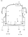
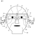
実施例1は、本開示の表示装置(具体的には、頭部装着型ディスプレイ,HMD)及び画像表示装置に関し、具体的には、第1の形態の画像表示装置に関する。実施例1の表示装置における画像表示装置の概念図を図1に示し、実施例1の表示装置を上方から眺めた模式図を図2に示し、実施例1の表示装置を正面から眺めた模式図を図3に示し、実施例1の表示装置を側方から眺めた模式図を図4Aに示す。また、反射型体積ホログラム回折格子の一部を拡大して示す模式的な断面図を図4Bに示し、画像表示装置を構成する導光板における光の伝播を図5に模式的に示す。 Example 1 relates to a display device (specifically, a head-mounted display, HMD) and an image display device of the present disclosure, and specifically relates to an image display device of a first form. FIG. 1 shows a conceptual diagram of the image display device in the display device of the first embodiment, FIG. 2 shows a schematic view of the display device of the first embodiment viewed from above, and a schematic view of the display device of the first embodiment viewed from the front. FIG. 4 shows a diagram, and FIG. 4A shows a schematic view of the display device of Example 1 viewed from the side. FIG. 4B is a schematic cross-sectional view showing a part of the reflective volume hologram diffraction grating in an enlarged manner, and FIG. 5 schematically shows light propagation in the light guide plate constituting the image display device.
実施例1あるいは後述する実施例2〜実施例4の表示装置は、より具体的には、頭部装着型ディスプレイ(HMD)であり、
(イ)観察者の頭部に装着されるフレーム(例えば、眼鏡型のフレーム10)、及び、
(ロ)フレーム10に取り付けられた画像表示装置100,200,300、
を備えている。尚、実施例1あるいは後述する実施例2〜実施例4の表示装置を、具体的には、2つの画像表示装置を備えた両眼型としたが、1つ備えた片眼型としてもよい。
More specifically, the display device of Example 1 or Example 2 to Example 4 described later is a head-mounted display (HMD).
(A) a frame (for example, a glasses-type frame 10) attached to the observer's head; and
(B) the
It has. In addition, although the display apparatus of Example 1 or Example 2 to Example 4 described later is specifically a binocular type including two image display apparatuses, it may be a single-eye type including one. .
そして、実施例1あるいは後述する実施例2〜実施例3における画像表示装置100,200は、
(A)画像形成装置111,211、
(B)画像形成装置111,211から出射された光が入射され、出射される光学装置(導光手段)120、
(C)画像形成装置111,211の温度を測定する温度測定装置125、及び、
(D)温度測定装置125による温度測定結果に基づき画像形成装置の動作を制御する制御装置18、
を備えている。更には、
(E)画像形成装置111,211から出射された光を平行光とする光学系(平行光出射光学系)112,254、
を備えており、光学系112,254にて平行光とされた光束が光学装置120に入射され、出射される。
And the
(A)
(B) an optical device (light guiding unit) 120 that receives and emits light emitted from the
(C) a
(D) a
It has. Furthermore,
(E) Optical systems (parallel light emitting optical systems) 112, 254 that make light emitted from the
, And the light beams converted into parallel light by the
尚、画像表示装置100,200,300は、フレームに、固定して取り付けられていてもよいし、着脱自在に取り付けられていてもよい。ここで、光学系112,254は、画像形成装置111,211と光学装置120との間に配置されている。そして、光学系112,254にて平行光とされた光束が、光学装置120に入射され、出射される。また、光学装置120は半透過型(シースルー型)である。具体的には、少なくとも観察者の両眼に対向する光学装置の部分(より具体的には、後述する導光板121及び第2偏向手段140)は、半透過(シースルー)である。
The
尚、実施例1あるいは後述する実施例2〜実施例3において、画像形成装置111,211の中心から出射され、光学系112,254の画像形成装置側節点を通過した光線(中心光線CL)の内、光学装置120に垂直に入射する中心入射光線が光学装置120に入射する点を光学装置中心点Oとし、光学装置中心点Oを通過し、光学装置120の軸線方向と平行な軸線をX軸、光学装置中心点Oを通過し、光学装置120の法線と一致する軸線をY軸とする。尚、第1偏向手段130の中心点が、光学装置中心点Oである。即ち、図5に示すように、画像表示装置100,200において、画像形成装置111,211の中心から出射され、光学系112,254の画像形成装置側節点を通過した中心入射光線CLは、導光板121に垂直に衝突する。云い換えれば、中心入射光線CLは、導光板121へ、入射角0度で入射する。そして、この場合、表示される画像の中心は、導光板121の第1面122の垂線方向に一致する。
In Example 1 or Examples 2 to 3 to be described later, a light beam (central light beam CL) emitted from the centers of the
実施例1あるいは後述する実施例2〜実施例3における光学装置120は、
(a)入射された光が内部を全反射により伝播した後、出射される導光板121、
(b)導光板121に入射された光が導光板121の内部で全反射されるように、導光板121に入射された光の少なくとも一部を偏向させる、反射鏡又は半透過鏡から成る第1偏向手段第1偏向手段130、及び、
(c)導光板121の内部を全反射により伝播した光を導光板121から出射させるために、導光板121の内部を全反射により伝播した光を偏向させる、回折格子部材から成る第2偏向手段140、
を備えている。ここで、具体的には、第2偏向手段140は、反射型体積ホログラム回折格子から成る。
The
(A) after the incident light propagates through the interior by total reflection, the
(B) A first mirror composed of a reflecting mirror or a semi-transmissive mirror that deflects at least a part of the light incident on the
(C) Second deflecting means comprising a diffraction grating member for deflecting light propagated through the
It has. Here, specifically, the
そして、実施例1あるいは後述する実施例2において、
画像形成装置111は、GaN系の半導体レーザ素子から成る光源153を備えており、
温度測定装置125は半導体レーザ素子の温度を測定し、
制御装置18によって半導体レーザ素子の波長を制御する。尚、制御装置18は、半導体レーザ素子に供給する電流を制御することによって半導体レーザ素子の波長を制御する。半導体レーザ素子は緑色又は青色を発光する。即ち、画像形成装置111,211は、例えば、単色(例えば、緑色)の画像を表示する。GaN系の半導体レーザ素子をパルス幅変調(PWM)方式に基づき駆動する場合、パルス高を制御すればよい。
And in Example 1 or Example 2 described later,
The
The
The
実施例1あるいは後述する実施例2〜実施例4において、温度測定装置125は、周知の温度測定装置、例えば、熱電対、測温抵抗体、サーミスタ、IC温度センサ等から構成されている。
In Embodiment 1 or Embodiments 2 to 4 described later, the
実施例1あるいは後述する実施例2〜実施例3において、第1偏向手段130は導光板121の内部に配設されており、第2偏向手段140は、導光板121の表面(具体的には、導光板121の第2面123)に配設されている。そして、第1偏向手段130は、導光板121に入射された光の少なくとも一部を反射し、第2偏向手段140は、導光板121の内部を全反射により伝播した光を、複数回に亙り、回折反射し、導光板121から平行光のまま第1面122から出射する。即ち、第1偏向手段130においては、導光板121に入射された平行光が導光板121の内部で全反射されるように、導光板121に入射された平行光が反射される。一方、第2偏向手段140においては、導光板121の内部を全反射により伝播した平行光が複数回に亙り回折反射され、導光板121から平行光の状態で、観察者の瞳21に向かって出射される。
In the first embodiment or the second to third embodiments described later, the
より具体的には、導光板121の内部に設けられた第1偏向手段130は、例えば、アルミニウム(Al)から成り、導光板121に入射された光を反射させる光反射膜(一種のミラー)から構成されている。第1偏向手段130は、導光板121の第1偏向手段130を設ける部分124を切り出すことで、導光板121に第1偏向手段130を形成すべき斜面を設け、係る斜面に光反射膜を真空蒸着した後、導光板121の切り出した部分124を第1偏向手段130に接着すればよい。
More specifically, the
一方、第2偏向手段140は、回折格子素子、具体的には反射型回折格子素子、より具体的には反射型体積ホログラム回折格子から成る。実施例1あるいは後述する実施例2〜実施例3において、第2偏向手段140は、1層の回折格子層が積層されて成る構成としている。尚、フォトポリマー材料から成る回折格子層には、1種類の波長帯域(あるいは、波長)に対応する干渉縞が形成されており、従来の方法で作製されている。回折格子層(回折光学素子)に形成された干渉縞のピッチは一定であり、干渉縞は直線状であり、Z軸に平行である。尚、第2偏向手段140の軸線はX軸と平行であり、法線はY軸と平行である。第2偏向手段140は、導光板121の第2面123に配設(接着)されている。
On the other hand, the
図4Bに反射型体積ホログラム回折格子の拡大した模式的な一部断面図を示す。反射型体積ホログラム回折格子には、傾斜角φを有する干渉縞が形成されている。ここで、傾斜角φとは、反射型体積ホログラム回折格子の表面と干渉縞の成す角度を指す。干渉縞は、反射型体積ホログラム回折格子の内部から表面に亙り、形成されている。干渉縞は、ブラッグ条件を満たしている。ここで、ブラッグ条件とは、以下の式(A)を満足する条件を指す。式(A)中、mは正の整数、λは波長、dは格子面のピッチ(干渉縞を含む仮想平面の法線方向の間隔)、Θは干渉縞へ入射する角度の余角を意味する。また、入射角ψにて回折格子部材に光が侵入した場合の、Θ、傾斜角φ、入射角ψの関係は、式(B)のとおりである。 FIG. 4B shows an enlarged schematic partial cross-sectional view of the reflective volume hologram diffraction grating. In the reflection type volume hologram diffraction grating, interference fringes having an inclination angle φ are formed. Here, the inclination angle φ refers to an angle formed between the surface of the reflective volume hologram diffraction grating and the interference fringes. The interference fringes are formed from the inside to the surface of the reflection type volume hologram diffraction grating. The interference fringes satisfy the Bragg condition. Here, the Bragg condition refers to a condition that satisfies the following formula (A). In equation (A), m is a positive integer, λ is the wavelength, d is the pitch of the grating plane (the interval in the normal direction of the imaginary plane including the interference fringes), and Θ is the angle of incidence of the incident on the interference fringes To do. In addition, when light enters the diffraction grating member at the incident angle ψ, the relationship among Θ, the tilt angle φ, and the incident angle ψ is as shown in Expression (B).
m・λ=2・d・sin(Θ) (A)
Θ=90°−(φ+ψ) (B)
m · λ = 2 · d · sin (Θ) (A)
Θ = 90 °-(φ + ψ) (B)
導光板121にあっては、平行光が内部を全反射により伝播した後、出射される。このとき、導光板121が薄く導光板121の内部を進行する光路が長いため、各画角によって第2偏向手段140に至るまでの全反射回数は異なっている。より詳細に述べれば、導光板121に入射する平行光のうち、第2偏向手段140に近づく方向の角度をもって入射する平行光の反射回数は、第2偏向手段140から離れる方向の角度をもって導光板121に入射する平行光の反射回数よりも少ない。これは、第1偏向手段130において反射される平行光であって、第2偏向手段140に近づく方向の角度をもって導光板121に入射する平行光の方が、これと逆方向の角度をもって導光板121に入射する平行光よりも、導光板121の内部を伝播していく光が導光板121の内面と衝突するときの導光板121の法線と成す角度が小さくなるからである。
In the
実施例1あるいは後述する実施例2〜実施例3において、導光板121は、光学ガラスやプラスチック材料から成る。そして、実施例1あるいは後述する実施例2〜実施例3において、導光板121は、導光板121の内部全反射による光伝播方向(X軸)と平行に延びる2つの平行面(第1面122及び第2面123)を有している。第1面122と第2面123とは対向している。そして、光入射面に相当する第1面122から平行光が入射され、内部を全反射により伝播した後、光出射面に相当する第1面122から出射される。但し、これに限定するものではなく、第2面123によって光入射面が構成され、第1面122によって光出射面が構成されていてもよい。
In Embodiment 1 or Embodiments 2 to 3 described later, the
実施例1において、画像形成装置111は、第1の構成の画像形成装置であり、2次元マトリクス状に配列された複数の画素を有する。具体的には、画像形成装置111は、反射型空間光変調装置150、及び、GaN系の半導体レーザ素子から成る光源153を備えている。各画像形成装置111全体は、筐体113(図1では、一点鎖線で示す)内に納められており、係る筐体113には開口部(図示せず)が設けられており、開口部を介して光学系(平行光出射光学系,コリメート光学系)112から光が出射される。反射型空間光変調装置150は、ライト・バルブとしてのLCOSから成る液晶表示装置(LCD)151、及び、光源153からの光の一部を反射して液晶表示装置151へと導き、且つ、液晶表示装置151によって反射された光の一部を通過させて光学系112へと導く偏光ビームスプリッター152から構成されている。液晶表示装置151は、2次元マトリクス状に配列された複数(例えば、640×480個)の画素(液晶セル)を備えている。偏光ビームスプリッター152は、周知の構成、構造を有する。光源153から出射された無偏光の光は、偏光ビームスプリッター152に衝突する。偏光ビームスプリッター152において、P偏光成分は通過し、系外に出射される。一方、S偏光成分は、偏光ビームスプリッター152において反射され、液晶表示装置151に入射し、液晶表示装置151の内部で反射され、液晶表示装置151から出射される。ここで、液晶表示装置151から出射した光の内、「白」を表示する画素から出射した光にはP偏光成分が多く含まれ、「黒」を表示する画素から出射した光にはS偏光成分が多く含まれる。従って、液晶表示装置151から出射され、偏光ビームスプリッター152に衝突する光の内、P偏光成分は、偏光ビームスプリッター152を通過し、光学系112へと導かれる。一方、S偏光成分は、偏光ビームスプリッター152において反射され、光源153に戻される。光学系112は、例えば、凸レンズから構成され、平行光を生成させるために、光学系112における焦点距離の所(位置)に画像形成装置111(より具体的には、液晶表示装置151)が配置されている。
In the first exemplary embodiment, the
フレーム10は、観察者の正面に配置されるフロント部11と、フロント部11の両端に蝶番12を介して回動自在に取り付けられた2つのテンプル部13と、各テンプル部13の先端部に取り付けられたモダン部(先セル、耳あて、イヤーパッドとも呼ばれる)14から成る。また、ノーズパッド(図示せず)が取り付けられている。即ち、フレーム10及びノーズパッドの組立体は、基本的には、通常の眼鏡と略同じ構造を有する。更には、各筐体113が、取付け部材19によって、着脱自在に、テンプル部13に取り付けられている。フレーム10は、金属又はプラスチックから作製されている。尚、各筐体113は、取付け部材19によってテンプル部13に着脱できないように取り付けられていてもよい。また、眼鏡を所有し、装着している観察者に対しては、観察者の所有する眼鏡のフレームのテンプル部に、各筐体113を取付け部材19によって着脱自在に取り付けてもよい。各筐体113を、テンプル部13の外側に取り付けてもよいし、テンプル部13の内側に取り付けてもよい。
The
更には、一方の画像形成装置111Aから延びる配線(信号線や電源線等)15が、テンプル部13、及び、モダン部14の内部を介して、モダン部14の先端部から外部に延び、制御装置(制御回路、制御手段)18に接続されている。更には、各画像形成装置111A,111Bはヘッドホン部16を備えており、各画像形成装置111A,111Bから延びるヘッドホン部用配線16’が、テンプル部13、及び、モダン部14の内部を介して、モダン部14の先端部からヘッドホン部16へと延びている。ヘッドホン部用配線16’は、より具体的には、モダン部14の先端部から、耳介(耳殻)の後ろ側を回り込むようにしてヘッドホン部16へと延びている。このような構成にすることで、ヘッドホン部16やヘッドホン部用配線16’が乱雑に配置されているといった印象を与えることがなく、すっきりとした表示装置とすることができる。
Furthermore, a wiring (a signal line, a power supply line, etc.) 15 extending from one
配線(信号線や電源線等)15は、上述したとおり、制御装置(制御回路)18に接続されている。そして、制御装置18において画像表示のための処理がなされる。制御装置18は周知の回路から構成することができる。
The wiring (signal line, power supply line, etc.) 15 is connected to the control device (control circuit) 18 as described above. Then, the
また、フロント部11の中央部分11’には、CCDあるいはCMOSセンサーから成る固体撮像素子とレンズ(これらは図示せず)とから構成された撮像装置17が、適切な取付部材(図示せず)によって取り付けられている。撮像装置17からの信号は、撮像装置17から延びる配線(図示せず)を介して、例えば、画像形成装置111Aに送出される。
Further, in the
一般に、半導体レーザ素子の発振波長(半導体レーザ素子から出射される波長λ)は、接合面の温度上昇に伴い、長波長側にシフトする。このような半導体レーザ素子から出射される波長λの長波長側へのシフトが生じると、前述したように、式(A)で表されるブラッグ条件にそって回折方向が変化することで、観察者が観察する画像にズレが生じる。ところで、GaN系化合物半導体層が積層されて成るGaN系の半導体レーザ素子は、駆動電流の増加に伴い、半導体レーザ素子の発振波長(半導体レーザ素子から出射される波長λ)は、短波長側にシフトする。従って、温度上昇に伴う半導体レーザ素子の発振波長の長波長側へのシフトを補償することができる。即ち、温度測定装置125によって光源(半導体レーザ素子)153の温度を測定する。光源153における温度変化が所定の範囲内にある場合には、ブラッグ条件からの逸脱が生じることがない。ところが、光源153における温度変化が所定の範囲から逸脱した場合、光源153の発熱に起因して光源153から出射される光の波長が増加する。その結果、ブラッグ条件からの逸脱が生じ、観察者が観察する画像の画質に低下が生じる。即ち、観察者が観察する画像にズレが生じる。従って、このような現象が生じた場合、制御装置18の制御下、光源153を構成するGaN系の半導体レーザ素子の駆動電流を増加させることで、光源153から出射される光の波長を短波長側にシフトさせ、元の波長に戻せばよい。尚、半導体レーザ素子の温度と駆動電流との関係を予め求めておき、係る関係を制御装置18に記憶させておけばよい。
In general, the oscillation wavelength of the semiconductor laser element (wavelength λ emitted from the semiconductor laser element) shifts to the longer wavelength side as the temperature of the bonding surface increases. When the wavelength λ emitted from the semiconductor laser element shifts to the long wavelength side, as described above, the diffraction direction changes according to the Bragg condition represented by the formula (A). Deviation occurs in an image observed by a person. By the way, in a GaN-based semiconductor laser element in which GaN-based compound semiconductor layers are stacked, the oscillation wavelength of the semiconductor laser element (wavelength λ emitted from the semiconductor laser element) is reduced to the short wavelength side as the drive current increases. shift. Therefore, it is possible to compensate for the shift of the oscillation wavelength of the semiconductor laser element to the longer wavelength side accompanying the temperature rise. That is, the temperature of the light source (semiconductor laser element) 153 is measured by the
以上のとおり、実施例1の画像表示装置あるいは表示装置にあっては、画像形成装置の温度を測定する温度測定装置、及び、温度測定装置による温度測定結果に基づき画像形成装置の動作を制御する制御装置を備えているので、光源から出射される光の波長の変動に起因した画像の画質低下を確実に回避することができる。 As described above, in the image display device or the display device according to the first embodiment, the temperature measurement device that measures the temperature of the image forming device and the operation of the image forming device are controlled based on the temperature measurement result by the temperature measurement device. Since the control device is provided, it is possible to reliably avoid a reduction in image quality due to a change in wavelength of light emitted from the light source.
実施例2は、実施例1の変形である。実施例2の表示装置(頭部装着型ディスプレイ)における画像表示装置200の概念図を図6に示すように、実施例2において、画像形成装置211は、第2の構成の画像形成装置から構成されている。即ち、光源251、及び、光源251から出射された平行光を走査する走査手段253を備えている。より具体的には、画像形成装置211は、
(イ)光源251、
(ロ)光源251から出射された光を平行光とするコリメート光学系252、
(ハ)コリメート光学系252から出射された平行光を走査する走査手段253、及び、
(ニ)走査手段253によって走査された平行光をリレーし、出射するリレー光学系254、
から構成されている。尚、画像形成装置211全体が筐体213(図6では、一点鎖線で示す)内に納められており、係る筐体213には開口部(図示せず)が設けられており、開口部を介してリレー光学系254から光が出射される。そして、各筐体213が、取付け部材19によって、着脱自在に、テンプル部13に取り付けられている。
The second embodiment is a modification of the first embodiment. FIG. 6 is a conceptual diagram of the
(A)
(B) a collimating
(C) scanning means 253 for scanning parallel light emitted from the collimating
(D) a relay
It is composed of Note that the entire
光源251は、実施例1と同様に、例えば、緑色を発光するGaN系の半導体レーザ素子から構成されている。そして、光源251から出射された光は、全体として正の光学的パワーを持つコリメート光学系252に入射し、平行光として出射される。そして、この平行光は、全反射ミラー256で反射され、マイクロミラーを二次元方向に回転自在とし、入射した平行光を2次元的に走査することができるMEMSから成る走査手段253によって水平走査及び垂直走査が行われ、一種の2次元画像化され、仮想の画素(画素数は、例えば、実施例1と同じとすることができる)が生成される。そして、仮想の画素からの光は、周知のリレー光学系から構成されたリレー光学系(平行光出射光学系)254を通過し、平行光とされた光束が光学装置120に入射する。
The
リレー光学系254にて平行光とされた光束が入射され、導光され、出射される光学装置120は、実施例1にて説明した光学装置と同じ構成、構造を有するので、詳細な説明は省略する。また、実施例2の表示装置も、上述したとおり、画像形成装置211が異なる点を除き、実質的に、実施例1の表示装置と同じ構成、構造を有するので、詳細な説明は省略する。
The
実施例3は、実施例1〜実施例2の変形であり、第2の形態の画像表示装置に関する。実施例3の画像表示装置において、
画像形成装置111,211は、半導体レーザ素子から成る光源を備えており、
温度測定装置125は半導体レーザ素子の温度を測定し、
制御装置18によって、画像形成装置111,211からの光の出射位置を制御する。
The third embodiment is a modification of the first to second embodiments and relates to the image display apparatus according to the second mode. In the image display device of Example 3,
The
The
The light emitting position from the
ここで、実施例3の画像表示装置において、半導体レーザ素子として、赤色を発光する赤色発光半導体レーザ素子を用いることが好ましいが、これに限定するものではなく、緑色を発光する緑色発光半導体レーザ素子、青色を発光する青色発光半導体レーザ素子を用いることもできる。 Here, in the image display device of Example 3, it is preferable to use a red light emitting semiconductor laser element that emits red as the semiconductor laser element. However, the present invention is not limited to this, and a green light emitting semiconductor laser element that emits green light. A blue light emitting semiconductor laser element that emits blue light can also be used.
具体的には、実施例3にあっても、温度測定装置125によって光源(半導体レーザ素子)153,251の温度を測定する。光源153,251における温度変化が所定の範囲内にある場合には、ブラッグ条件からの逸脱が生じることがない。ところが、光源153,251における温度変化が所定の範囲から逸脱した場合、光源153,251の発熱に起因して光源153,251から出射される光の波長が増加する。その結果、ブラッグ条件にそって回折方向が変化することで、観察者が観察する画像にズレが生じる。従って、このような現象が生じた場合、画像形成装置111,211に送出する画像信号を補償してずれを無くせばよい。より具体的には、画像の水平方向の移動のためには、表示位置補正信号として、画像の水平方向の位置を+i画素あるいは−i画素分、変える信号を制御装置18において生成すればよい。あるいは又、水平同期信号のタイミングを+i画素あるいは−i画素分、変える信号を制御装置18において生成すればよい。また、画像の垂直方向の移動のためには、表示位置補正信号として、画像の垂直方向の位置を+j画素あるいは−j画素分、変える信号を制御装置18において生成すればよく、あるいは又、垂直同期信号のタイミングを+j画素あるいは−j画素分、変える信号を制御装置18において生成すればよい。即ち、画像のメモリ読み出し位置を、タイミング的に、遅らす、又は、早めることにより実現することができ、あるいは、垂直同期信号と水平同期信号のタイミングをずらすことによって実現することができる。そして、半導体レーザ素子の温度と表示位置補正信号との関係を予め求めておき、係る関係を制御装置18に記憶させておけばよく、制御装置18において、画像を形成するための画像信号に対して表示位置補正信号を加えればよい。あるいは又、光学装置120から出射される画像に生じる歪みを補償するために、画像形成装置111,211に送出する画像信号に、画像に生じる歪みを補償するための信号を加重して、歪みを除去してもよい。即ち、温度測定装置125の検出結果に基づき、光学装置120から出射される画像に生じる歪みを補償するための信号が画像形成装置111,211に送出される構成とすることもできる。
Specifically, even in the third embodiment, the temperature of the light sources (semiconductor laser elements) 153 and 251 is measured by the
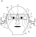
実施例4も、実施例1〜実施例3における画像表示装置、表示装置における光学装置の変形である。実施例4の表示装置を正面から眺めた模式図を図7に示し、上方から眺めた模式図を図8に示す。 The fourth embodiment is also a modification of the image display device in the first to third embodiments and the optical device in the display device. A schematic view of the display device of Example 4 as viewed from the front is shown in FIG. 7, and a schematic view as seen from above is shown in FIG.
実施例4において、画像表示装置300を構成する光学装置320は、画像形成装置111A,111Bから出射された光が入射され、観察者の瞳21に向かって出射される半透過ミラーから構成されている。光学装置320には、第2偏向手段140が配されている。尚、実施例4において、画像形成装置111A,111Bから出射された光は、ガラス板やプラスチック板等の透明な部材321の内部を伝播して光学装置320(半透過ミラー)に入射する構造としているが、空気中を伝播して光学装置320に入射する構造としてもよい。また、画像形成装置は、実施例2において説明した画像形成装置211とすることもできる。また、画像形成装置111,211からの光を、第1偏向手段130を介して光学装置320に到達するように構成してもよいし、画像形成装置111,211からの光が、直接、光学装置320に到達するように構成してもよい。
In the fourth exemplary embodiment, the optical device 320 included in the image display device 300 includes a semi-transmissive mirror that receives the light emitted from the
各画像形成装置111A,111Bは、フロント部11に、例えば、ビスを用いて取り付けられている。また、部材321が各画像形成装置111A,111Bに取り付けられ、光学装置320(半透過ミラー)が部材321に取り付けられている。実施例4の表示装置は、以上の相違点を除き、実質的に、実施例1〜実施例3の表示装置と同じ構成、構造を有するので、詳細な説明は省略する。
Each of the
以上、本開示を好ましい実施例に基づき説明したが、本開示はこれらの実施例に限定するものではない。実施例において説明した表示装置(頭部装着型ディスプレイ)、画像表示装置の構成、構造は例示であり、適宜変更することができる。例えば、導光板に表面レリーフ型ホログラム(米国特許第20040062505A1参照)を配置してもよい。光学装置にあっては、回折格子素子を透過型回折格子素子から構成することもできる。あるいは又、回折格子素子を、反射型ブレーズド回折格子素子とすることもできる。 Although the present disclosure has been described based on the preferred embodiments, the present disclosure is not limited to these embodiments. The configurations and structures of the display device (head-mounted display) and the image display device described in the embodiments are examples, and can be appropriately changed. For example, a surface relief hologram (see US 20040062505A1) may be disposed on the light guide plate. In the optical apparatus, the diffraction grating element can also be composed of a transmission type diffraction grating element. Alternatively, the diffraction grating element can be a reflective blazed diffraction grating element.
画像形成装置において表示する画像に関する情報やデータは、表示装置に備えられていてもよいし、所謂クラウドコンピュータに情報やデータを記録しておいてもよい。後者の場合、表示装置に通信手段、例えば、携帯電話機やスマートフォンを備えることによって、あるいは又、表示装置と通信手段とを組み合わせることによって、クラウドコンピュータと表示装置との間での各種情報やデータの授受、交換を行うことができる。 Information and data relating to an image displayed in the image forming apparatus may be provided in the display device, or information and data may be recorded in a so-called cloud computer. In the latter case, various information and data between the cloud computer and the display device can be obtained by providing the display device with communication means, for example, a mobile phone or a smartphone, or by combining the display device and communication means. Can exchange, exchange.
実施例においては、画像形成装置111,211は、単色(例えば、緑色)の画像を表示するとして説明したが、画像形成装置111,211はカラー画像を表示することもでき、この場合、光源を、例えば、赤色、緑色、青色のそれぞれを出射する光源から構成すればよい。具体的には、例えば、赤色発光半導体レーザ素子、緑色発光半導体レーザ素子、青色発光半導体レーザ素子のそれぞれから出射された赤色レーザ光、緑色レーザ光及び青色レーザ光をライトパイプを用いて混色、輝度均一化を行うことで白色光を得ればよい。尚、光源のそれぞれを、赤色発光半導体レーザ素子、緑色発光半導体レーザ素子、青色発光半導体レーザ素子から構成する場合、赤色発光半導体レーザ素子によって形成される赤色の画像に関しては、温度測定装置の温度測定結果に基づき、画像形成装置から出射される画像の位置を制御し、緑色発光半導体レーザ素子及び青色発光半導体レーザ素子によって形成される緑色及び青色の画像に関しては、温度測定装置の温度測定結果に基づき、画像形成装置から出射される画像の位置を制御してもよいし、温度測定装置の温度測定結果に基づき、光源から出射される光の波長を制御してもよい。
In the embodiment, the
画像形成装置の変形例として、例えば、図9に概念図を示すような、半導体レーザ素子から成る発光素子601が2次元マトリクス状に配列された発光パネルから成り、発光素子601のそれぞれの発光/非発光状態を制御することで、発光素子601の発光状態を直接的に視認させることで画像を表示する、アクティブマトリックスタイプの画像形成装置とすることもできる。この画像形成装置から出射された光は、コリメート光学系112を介して導光板121に入射される。尚、以下の説明においても、発光素子は、半導体レーザ素子から成る。
As a modified example of the image forming apparatus, for example, as shown in a conceptual diagram in FIG. 9, a
あるいは又、図10に概念図を示すように、
(α)赤色を発光する赤色発光素子601Rが2次元マトリクス状に配列された赤色発光パネル611R、
(β)緑色を発光する緑色発光素子601Gが2次元マトリクス状に配列された緑色発光パネル611G、及び、
(γ)青色を発光する青色発光素子601Bが2次元マトリクス状に配列された青色発光パネル611B、並びに、
(δ)赤色発光パネル611R、緑色発光パネル611G及び青色発光パネル611Bから出射された光を1本の光路に纏めるための手段(例えば、ダイクロイック・プリズム603)、
を備えており、
赤色発光素子601R、緑色発光素子601G及び青色発光素子601Bのそれぞれの発光/非発光状態を制御するカラー表示の画像形成装置とすることもできる。この画像形成装置から出射された光も、コリメート光学系112を介して導光板121に入射される。尚、参照番号612は、発光素子から出射された光を集光するためのマイクロレンズである。
Alternatively, as shown in the conceptual diagram of FIG.
(Α) a red
(Β) a green
(Γ) Blue
(Δ) means (for example, dichroic prism 603) for collecting the light emitted from the red
With
A color display image forming apparatus that controls the light emission / non-light emission state of each of the red
あるいは又、発光素子601R,601G,601Bが2次元マトリクス状に配列された発光パネル611R,611G,611B等から成る画像形成装置の概念図を図11に示すが、発光パネル611R,611G,611Bから出射された光は、光通過制御装置604R,604G,604Bによって通過/非通過が制御され、ダイクロイック・プリズム603に入射し、これらの光の光路は1本の光路に纏められ、コリメート光学系112を介して導光板121に入射される。
Alternatively, FIG. 11 shows a conceptual diagram of an image forming apparatus including
あるいは又、発光素子601R,601G,601Bが2次元マトリクス状に配列された発光パネル611R,611G,611B等から成る画像形成装置の概念図を図12に示すが、発光パネル611R,611G,611Bから出射された光は、ダイクロイック・プリズム603に入射し、これらの光の光路は1本の光路に纏められ、ダイクロイック・プリズム603から出射したこれらの光は光通過制御装置604によって通過/非通過が制御され、コリメート光学系112を介して導光板121に入射される。
Alternatively, FIG. 12 shows a conceptual diagram of an image forming apparatus composed of light emitting
あるいは又、図13に示すように、赤色を発光する発光素子601R、及び、赤色を発光する発光素子601Rから出射された出射光の通過/非通過を制御するための一種のライト・バルブである光通過制御装置(例えば、液晶表示装置604R)、緑色を発光する発光素子601G、及び、緑色を発光する発光素子601Gから出射された出射光の通過/非通過を制御するための一種のライト・バルブである光通過制御装置(例えば、液晶表示装置604G)、青色を発光する発光素子601B、及び、青色を発光する発光素子601Bから出射された出射光の通過/非通過を制御するための一種のライト・バルブである光通過制御装置(例えば、液晶表示装置604B)、並びに、これらの発光素子601R,601G,601Bから出射された光を案内する光案内部材602、及び、1本の光路に纏めるための手段(例えば、ダイクロイック・プリズム603)を備えた画像形成装置とすることもできる。そして、ダイクロイック・プリズム603から出射したこれらの光は、コリメート光学系112を介して導光板121に入射される。
Alternatively, as shown in FIG. 13, the
尚、本開示は、以下のような構成を取ることもできる。
[A01]《画像表示装置》
(A)画像形成装置、
(B)画像形成装置から出射された光が入射され、出射される光学装置、
(C)画像形成装置の温度を測定する温度測定装置、及び、
(D)温度測定装置による温度測定結果に基づき画像形成装置の動作を制御する制御装置、
を備えている画像表示装置。
[A02]《第1の形態の画像表示装置》
画像形成装置は、GaN系の半導体レーザ素子から成る光源を備えており、
温度測定装置は半導体レーザ素子の温度を測定し、
制御装置によって半導体レーザ素子の波長を制御する[A01]に記載の画像表示装置。
[A03]制御装置は、半導体レーザ素子に供給する電流を制御することによって半導体レーザ素子の波長を制御する[A02]に記載の画像表示装置。
[A04]半導体レーザ素子は緑色又は青色を発光する[A02]又は[A03]に記載の画像表示装置。
[A05]《第2の形態の画像表示装置》
画像形成装置は、半導体レーザ素子から成る光源を備えており、
温度測定装置は半導体レーザ素子の温度を測定し、
制御装置によって、画像形成装置からの光の出射位置を制御する[A01]に記載の画像表示装置。
[A06]半導体レーザ素子は赤色を発光する[A05]に記載の画像表示装置。
[A07]画像形成装置は、半導体レーザ素子から成る光源を備えており、
温度測定装置は半導体レーザ素子の温度を測定し、
制御装置によって、光学装置から出射される画像に生じる歪みを補償するための信号が画像形成装置に送出される[A01]に記載の画像表示装置。
[A08]光学装置は、
(a)入射された光が内部を全反射により伝播した後、出射される導光板、
(b)導光板に入射された光が導光板の内部で全反射されるように、導光板に入射された光の少なくとも一部を偏向させる、反射鏡又は半透過鏡から成る第1偏向手段、及び、
(c)導光板の内部を全反射により伝播した光を導光板から出射させるために、導光板の内部を全反射により伝播した光を偏向させる、回折格子部材から成る第2偏向手段、
を備えている[A01]乃至[A07]のいずれか1項に記載の画像表示装置。
[B01]《表示装置》
(イ)観察者の頭部に装着されるフレーム、及び、
(ロ)フレームに取り付けられた画像表示装置、
を備えた表示装置であって、
画像表示装置は、
(A)画像形成装置、
(B)画像形成装置から出射された光が入射され、出射される光学装置、
(C)画像形成装置の温度を測定する温度測定装置、及び、
(D)温度測定装置による温度測定結果に基づき画像形成装置の動作を制御する制御装置、
を備えている表示装置。
「B02]《表示装置》
(イ)観察者の頭部に装着されるフレーム、及び、
(ロ)フレームに取り付けられた画像表示装置、
を備えた表示装置であって、
画像表示装置は、[A01]乃至[A08]のいずれか1項に記載の画像表示装置から成る表示装置。
In addition, this indication can also take the following structures.
[A01] << Image display device >>
(A) an image forming apparatus,
(B) an optical device that receives and emits light emitted from the image forming apparatus;
(C) a temperature measuring device for measuring the temperature of the image forming apparatus, and
(D) a control device that controls the operation of the image forming apparatus based on the temperature measurement result by the temperature measurement device;
An image display device comprising:
[A02] << Image Display Device of First Form >>
The image forming apparatus includes a light source composed of a GaN-based semiconductor laser element,
The temperature measuring device measures the temperature of the semiconductor laser element,
The image display device according to [A01], wherein the wavelength of the semiconductor laser element is controlled by the control device.
[A03] The image display apparatus according to [A02], wherein the control device controls the wavelength of the semiconductor laser element by controlling a current supplied to the semiconductor laser element.
[A04] The image display device according to [A02] or [A03], in which the semiconductor laser element emits green or blue light.
[A05] << Image Display Device of Second Embodiment >>
The image forming apparatus includes a light source composed of a semiconductor laser element,
The temperature measuring device measures the temperature of the semiconductor laser element,
The image display device according to [A01], wherein a light emission position from the image forming device is controlled by a control device.
[A06] The image display device according to [A05], in which the semiconductor laser element emits red light.
[A07] The image forming apparatus includes a light source including a semiconductor laser element.
The temperature measuring device measures the temperature of the semiconductor laser element,
The image display device according to [A01], wherein a signal for compensating for distortion generated in an image emitted from the optical device is sent to the image forming device by the control device.
[A08] The optical device
(A) A light guide plate that is emitted after incident light propagates through the interior by total reflection;
(B) First deflecting means comprising a reflecting mirror or a semi-transmissive mirror for deflecting at least part of the light incident on the light guide plate so that the light incident on the light guide plate is totally reflected inside the light guide plate. ,as well as,
(C) a second deflecting means comprising a diffraction grating member for deflecting the light propagated in the light guide plate by total reflection in order to emit the light propagated in the light guide plate by total reflection from the light guide plate;
The image display device according to any one of [A01] to [A07].
[B01] << Display device >>
(A) a frame to be worn on the observer's head; and
(B) an image display device attached to the frame;
A display device comprising:
The image display device
(A) an image forming apparatus,
(B) an optical device that receives and emits light emitted from the image forming apparatus;
(C) a temperature measuring device for measuring the temperature of the image forming apparatus, and
(D) a control device that controls the operation of the image forming apparatus based on the temperature measurement result by the temperature measurement device;
A display device comprising:
“B02” << Display device >>
(A) a frame to be worn on the observer's head; and
(B) an image display device attached to the frame;
A display device comprising:
An image display device comprises the image display device according to any one of [A01] to [A08].
10・・・フレーム、11・・・フロント部、11’・・・フロント部の中央部分、12・・・蝶番、13・・・テンプル部、14・・・モダン部、15・・・配線(信号線や電源線等)、16・・・ヘッドホン部、16’・・・ヘッドホン部用配線、17・・・撮像装置、18・・・制御装置(制御回路)、19・・・取付け部材、21・・・瞳、100,200,300・・・画像表示装置、111,111A,111B,211・・・画像形成装置、112・・・光学系(コリメート光学系)、113,213・・・筐体、120・・・光学装置(導光手段)、121・・・導光板、122・・・導光板の第1面、123・・・導光板の第2面、124・・・導光板の一部分、125・・・温度測定装置、130・・・第1偏向手段、140・・・第2偏向手段、150・・・反射型空間光変調装置、151・・・液晶表示装置(LCD)、152・・・偏光ビームスプリッター、153・・・光源、251・・・光源、252・・・コリメート光学系、253・・・走査手段、254・・・光学系(リレー光学系)、255・・・クロスプリズム、256・・・全反射ミラー、320・・・光学装置(半透過ミラー)、321・・・透明な部材、601,601R,601G,601B・・・発光素子、602・・・光案内部材、603・・・ダイクロイック・プリズム、604,604R,604G,604B・・・光通過制御装置、611R,611G,611B・・・発光パネル、612・・・マイクロレンズ
DESCRIPTION OF
Claims (8)
(B)画像形成装置から出射された光が入射され、出射される光学装置、
(C)画像形成装置の温度を測定する温度測定装置、及び、
(D)温度測定装置による温度測定結果に基づき画像形成装置の動作を制御する制御装置、
を備えている画像表示装置。 (A) an image forming apparatus,
(B) an optical device that receives and emits light emitted from the image forming apparatus;
(C) a temperature measuring device for measuring the temperature of the image forming apparatus, and
(D) a control device that controls the operation of the image forming apparatus based on the temperature measurement result by the temperature measurement device;
An image display device comprising:
温度測定装置は半導体レーザ素子の温度を測定し、
制御装置によって半導体レーザ素子の波長を制御する請求項1に記載の画像表示装置。 The image forming apparatus includes a light source composed of a GaN-based semiconductor laser element,
The temperature measuring device measures the temperature of the semiconductor laser element,
The image display device according to claim 1, wherein the wavelength of the semiconductor laser element is controlled by the control device.
温度測定装置は半導体レーザ素子の温度を測定し、
制御装置によって、画像形成装置からの光の出射位置を制御する請求項1に記載の画像表示装置。 The image forming apparatus includes a light source composed of a semiconductor laser element,
The temperature measuring device measures the temperature of the semiconductor laser element,
The image display device according to claim 1, wherein a light emission position from the image forming device is controlled by the control device.
(a)入射された光が内部を全反射により伝播した後、出射される導光板、
(b)導光板に入射された光が導光板の内部で全反射されるように、導光板に入射された光の少なくとも一部を偏向させる、反射鏡又は半透過鏡から成る第1偏向手段、及び、
(c)導光板の内部を全反射により伝播した光を導光板から出射させるために、導光板の内部を全反射により伝播した光を偏向させる、回折格子部材から成る第2偏向手段、
を備えている請求項1に記載の画像表示装置。 The optical device
(A) A light guide plate that is emitted after incident light propagates through the interior by total reflection;
(B) First deflecting means comprising a reflecting mirror or a semi-transmissive mirror for deflecting at least part of the light incident on the light guide plate so that the light incident on the light guide plate is totally reflected inside the light guide plate. ,as well as,
(C) a second deflecting means comprising a diffraction grating member for deflecting the light propagated in the light guide plate by total reflection in order to emit the light propagated in the light guide plate by total reflection from the light guide plate;
The image display device according to claim 1, further comprising:
(ロ)フレームに取り付けられた画像表示装置、
を備えた表示装置であって、
画像表示装置は、
(A)画像形成装置、
(B)画像形成装置から出射された光が入射され、出射される光学装置、
(C)画像形成装置の温度を測定する温度測定装置、及び、
(D)温度測定装置による温度測定結果に基づき画像形成装置の動作を制御する制御装置、
を備えている表示装置。 (A) a frame to be worn on the observer's head; and
(B) an image display device attached to the frame;
A display device comprising:
The image display device
(A) an image forming apparatus,
(B) an optical device that receives and emits light emitted from the image forming apparatus;
(C) a temperature measuring device for measuring the temperature of the image forming apparatus, and
(D) a control device that controls the operation of the image forming apparatus based on the temperature measurement result by the temperature measurement device;
A display device comprising:
Priority Applications (6)
| Application Number | Priority Date | Filing Date | Title |
|---|---|---|---|
| JP2014023138A JP2015148782A (en) | 2014-02-10 | 2014-02-10 | Image display device and display device |
| EP18204973.4A EP3470920B1 (en) | 2014-02-10 | 2014-12-19 | Image display device and display apparatus |
| EP14199451.7A EP2905655B1 (en) | 2014-02-10 | 2014-12-19 | Image display device and display apparatus |
| US14/612,710 US10477174B2 (en) | 2014-02-10 | 2015-02-03 | Image display device and display apparatus |
| CN201910020957.5A CN110082912B (en) | 2014-02-10 | 2015-02-03 | Image display device and display apparatus |
| CN201510055500.XA CN104834092B (en) | 2014-02-10 | 2015-02-03 | Image display device and display equipment |
Applications Claiming Priority (1)
| Application Number | Priority Date | Filing Date | Title |
|---|---|---|---|
| JP2014023138A JP2015148782A (en) | 2014-02-10 | 2014-02-10 | Image display device and display device |
Publications (2)
| Publication Number | Publication Date |
|---|---|
| JP2015148782A true JP2015148782A (en) | 2015-08-20 |
| JP2015148782A5 JP2015148782A5 (en) | 2016-03-24 |
Family
ID=52146263
Family Applications (1)
| Application Number | Title | Priority Date | Filing Date |
|---|---|---|---|
| JP2014023138A Pending JP2015148782A (en) | 2014-02-10 | 2014-02-10 | Image display device and display device |
Country Status (4)
| Country | Link |
|---|---|
| US (1) | US10477174B2 (en) |
| EP (2) | EP3470920B1 (en) |
| JP (1) | JP2015148782A (en) |
| CN (2) | CN110082912B (en) |
Cited By (6)
| Publication number | Priority date | Publication date | Assignee | Title |
|---|---|---|---|---|
| WO2017033601A1 (en) * | 2015-08-25 | 2017-03-02 | ソニー株式会社 | Display device and display device adjustment method |
| JP2017134240A (en) * | 2016-01-28 | 2017-08-03 | セイコーエプソン株式会社 | Electrooptical device, and control method for the same |
| US10203503B2 (en) | 2016-03-23 | 2019-02-12 | Seiko Epson Corporation | Image display apparatus and optical element having light guide plate with grating pitches on light incident and emitting sections thereof |
| KR20190041050A (en) * | 2017-10-11 | 2019-04-22 | 주식회사 카이비전 | Display apparatus using wave guide and image display method for the same |
| JP2020521174A (en) * | 2017-05-18 | 2020-07-16 | アリゾナ ボード オブ リージェンツ オン ビハーフ オブ ザ ユニバーシティ オブ アリゾナ | Multi-layer high dynamic range head-mounted display |
| JP7451534B2 (en) | 2018-12-28 | 2024-03-18 | マジック リープ, インコーポレイテッド | Virtual and augmented reality display system with emissive microdisplay |
Families Citing this family (30)
| Publication number | Priority date | Publication date | Assignee | Title |
|---|---|---|---|---|
| JP5434848B2 (en) | 2010-08-18 | 2014-03-05 | ソニー株式会社 | Display device |
| JP5780129B2 (en) | 2011-11-22 | 2015-09-16 | ソニー株式会社 | Light beam expansion device, image display device, and optical device |
| JP5879973B2 (en) | 2011-11-30 | 2016-03-08 | ソニー株式会社 | Light reflecting member, light beam extending device, image display device, and optical device |
| EP2808725B1 (en) | 2012-01-24 | 2018-09-26 | Sony Corporation | Head-mounted display device with a light-shielding member |
| JP6145966B2 (en) | 2012-05-09 | 2017-06-14 | ソニー株式会社 | Display device |
| CN104204905B (en) | 2013-01-10 | 2016-11-23 | 索尼公司 | Image display, video generation device and transmissive spatial optic modulating device |
| JP6123342B2 (en) | 2013-02-20 | 2017-05-10 | ソニー株式会社 | Display device |
| CN108132537B (en) | 2013-04-11 | 2021-03-16 | 索尼公司 | Display device |
| EP2985652A4 (en) | 2013-04-11 | 2016-12-14 | Sony Corp | Image display device and display device |
| JP6367529B2 (en) | 2013-06-25 | 2018-08-01 | ソニー株式会社 | Display device, display control method, display control device, and electronic apparatus |
| EP3018524B1 (en) | 2013-07-04 | 2023-03-29 | Sony Group Corporation | Display device |
| US9952435B2 (en) | 2013-07-16 | 2018-04-24 | Sony Corporation | Display apparatus having curved image forming apparatus |
| US10534172B2 (en) | 2013-07-16 | 2020-01-14 | Sony Corporation | Display apparatus |
| JP6314518B2 (en) | 2014-02-10 | 2018-04-25 | ソニー株式会社 | Image display device and display device |
| JP6391952B2 (en) | 2014-03-17 | 2018-09-19 | ソニー株式会社 | Display device and optical device |
| JP2015184560A (en) | 2014-03-25 | 2015-10-22 | ソニー株式会社 | Light guide device, image display device, and display device |
| JP2015184561A (en) | 2014-03-25 | 2015-10-22 | ソニー株式会社 | Light guide device, image display device, and display device |
| KR102262215B1 (en) * | 2014-09-01 | 2021-06-08 | 삼성전자주식회사 | Backlight unit and holographic display having the same |
| FR3046850B1 (en) * | 2016-01-15 | 2018-01-26 | Universite De Strasbourg | IMPROVED OPTICAL GUIDE AND OPTICAL SYSTEM COMPRISING SUCH AN OPTICAL GUIDE |
| JP6512452B2 (en) * | 2016-09-23 | 2019-05-15 | 京セラドキュメントソリューションズ株式会社 | Adjustment work support system |
| CN108267859B (en) * | 2017-01-12 | 2021-08-20 | 胡大文 | Display equipment for displaying 3D multimedia |
| CN108873327B (en) * | 2017-05-16 | 2021-03-05 | 中强光电股份有限公司 | Head-mounted display device |
| US10409066B2 (en) | 2017-01-19 | 2019-09-10 | Coretronic Corporation | Head-mounted display device with waveguide elements |
| CN108873326A (en) | 2017-05-16 | 2018-11-23 | 中强光电股份有限公司 | Head-mounted display apparatus |
| US10502956B2 (en) | 2017-06-27 | 2019-12-10 | Microsoft Technology Licensing, Llc | Systems and methods of reducing temperature gradients in optical waveguides |
| CN107462993A (en) * | 2017-09-04 | 2017-12-12 | 北京灵犀微光科技有限公司 | Image display device |
| CN109946907A (en) | 2017-12-20 | 2019-06-28 | 中强光电股份有限公司 | Projection arrangement |
| US11668927B2 (en) * | 2018-01-23 | 2023-06-06 | Google Llc | Wavelength stabilization of laser diodes by temperature control |
| US11073689B2 (en) * | 2018-08-31 | 2021-07-27 | Google Llc | Method and system for calibrating a wearable heads-up display to produce aligned virtual images in an eye space |
| CN113126299B (en) * | 2021-03-10 | 2023-02-17 | 北京至格科技有限公司 | Projection ray apparatus and head-mounted smart machine |
Citations (6)
| Publication number | Priority date | Publication date | Assignee | Title |
|---|---|---|---|---|
| JP2011090076A (en) * | 2009-10-21 | 2011-05-06 | Panasonic Corp | Image display device |
| WO2011132407A1 (en) * | 2010-04-20 | 2011-10-27 | パナソニック株式会社 | Image display device |
| WO2012132289A1 (en) * | 2011-03-25 | 2012-10-04 | パナソニック株式会社 | Dispay device |
| WO2013057799A1 (en) * | 2011-10-19 | 2013-04-25 | パイオニア株式会社 | Display device, head-mounted display, display method and display program |
| JP2013190658A (en) * | 2012-03-14 | 2013-09-26 | Sony Corp | Image display device and image generating device |
| JP2014194500A (en) * | 2013-03-29 | 2014-10-09 | Funai Electric Co Ltd | Projector and head-up display device |
Family Cites Families (46)
| Publication number | Priority date | Publication date | Assignee | Title |
|---|---|---|---|---|
| JPH10301055A (en) | 1997-04-25 | 1998-11-13 | Sony Corp | Image display device |
| KR20020094288A (en) * | 2001-06-08 | 2002-12-18 | 주식회사 엘지이아이 | Clock phase correction apparatus |
| US20030015697A1 (en) * | 2001-07-20 | 2003-01-23 | Motorola, Inc. | Fabrication of an optical transmitter within a semiconductor structure |
| JP4569942B2 (en) | 2002-09-26 | 2010-10-27 | 三菱電機株式会社 | Optical active device |
| WO2004097498A1 (en) * | 2003-04-28 | 2004-11-11 | Nikon Corporation | Image combiner and image display |
| WO2007007733A1 (en) * | 2005-07-11 | 2007-01-18 | Matsushita Electric Industrial Co., Ltd. | Light source, light source device, laser image forming device and integrated circuit |
| KR100758987B1 (en) * | 2006-09-26 | 2007-09-17 | 삼성전자주식회사 | A led lighting device and a method for controlling the same |
| CN201083877Y (en) * | 2007-09-07 | 2008-07-09 | 沈文龙 | Metallurgical microscope illuminating apparatus |
| CN101608772B (en) * | 2008-06-18 | 2012-09-05 | 海洋王照明科技股份有限公司 | Focusing device of lamp |
| JP2010039086A (en) | 2008-08-01 | 2010-02-18 | Sony Corp | Illumination optical apparatus and virtual image display device |
| JP5321011B2 (en) | 2008-11-25 | 2013-10-23 | ソニー株式会社 | Image signal processing apparatus, image signal processing method, and image projection apparatus |
| US8804247B2 (en) * | 2009-12-14 | 2014-08-12 | Panasonic Corporation | Transmissive display device |
| CN201667701U (en) * | 2010-03-23 | 2010-12-08 | 福州开发区鸿发光电子技术有限公司 | Intelligent high speed ball with built-in and variable angle infrared illumination system |
| JP5678460B2 (en) | 2010-04-06 | 2015-03-04 | ソニー株式会社 | Head-mounted display |
| JP5499854B2 (en) * | 2010-04-08 | 2014-05-21 | ソニー株式会社 | Optical position adjustment method for head mounted display |
| JP5494153B2 (en) | 2010-04-08 | 2014-05-14 | ソニー株式会社 | Image display method for head mounted display |
| CN101867151B (en) * | 2010-07-08 | 2014-04-23 | 华中科技大学 | Automatic compensating circuit for uncooled semiconductor laser wavelength temperature-following drift |
| JP5434848B2 (en) | 2010-08-18 | 2014-03-05 | ソニー株式会社 | Display device |
| WO2012042744A1 (en) * | 2010-10-01 | 2012-04-05 | パナソニック株式会社 | Display device, mobile body, and control device |
| JP5598281B2 (en) | 2010-11-19 | 2014-10-01 | ソニー株式会社 | Projection display system |
| JP5655626B2 (en) | 2011-02-24 | 2015-01-21 | ソニー株式会社 | Image processing apparatus, image processing method, and program |
| JP5408278B2 (en) * | 2011-03-28 | 2014-02-05 | カシオ計算機株式会社 | Projection apparatus, projection method, and program |
| JP2012252091A (en) * | 2011-06-01 | 2012-12-20 | Sony Corp | Display apparatus |
| JP5780129B2 (en) | 2011-11-22 | 2015-09-16 | ソニー株式会社 | Light beam expansion device, image display device, and optical device |
| JP5879973B2 (en) | 2011-11-30 | 2016-03-08 | ソニー株式会社 | Light reflecting member, light beam extending device, image display device, and optical device |
| EP2808725B1 (en) | 2012-01-24 | 2018-09-26 | Sony Corporation | Head-mounted display device with a light-shielding member |
| CN103368060B (en) * | 2012-03-28 | 2017-04-12 | 上海瀚宇光纤通信技术有限公司 | wavelength adjusting device |
| JP6145966B2 (en) | 2012-05-09 | 2017-06-14 | ソニー株式会社 | Display device |
| JP2013258357A (en) * | 2012-06-14 | 2013-12-26 | Mitsubishi Electric Corp | Semiconductor light source device |
| JP5929567B2 (en) | 2012-07-03 | 2016-06-08 | ソニー株式会社 | Image signal processing apparatus, image signal processing method, and program |
| US9059555B2 (en) * | 2012-09-12 | 2015-06-16 | Innovative Photonic Solutions | Wavelength-stabilized diode laser |
| US9720231B2 (en) * | 2012-09-26 | 2017-08-01 | Dolby Laboratories Licensing Corporation | Display, imaging system and controller for eyewear display device |
| CN104204905B (en) | 2013-01-10 | 2016-11-23 | 索尼公司 | Image display, video generation device and transmissive spatial optic modulating device |
| JP6123342B2 (en) | 2013-02-20 | 2017-05-10 | ソニー株式会社 | Display device |
| CN108132537B (en) | 2013-04-11 | 2021-03-16 | 索尼公司 | Display device |
| EP2985652A4 (en) | 2013-04-11 | 2016-12-14 | Sony Corp | Image display device and display device |
| JP2014225725A (en) | 2013-05-15 | 2014-12-04 | ソニー株式会社 | Display device and light source for image display device |
| JP6367529B2 (en) | 2013-06-25 | 2018-08-01 | ソニー株式会社 | Display device, display control method, display control device, and electronic apparatus |
| EP3018524B1 (en) | 2013-07-04 | 2023-03-29 | Sony Group Corporation | Display device |
| US9952435B2 (en) | 2013-07-16 | 2018-04-24 | Sony Corporation | Display apparatus having curved image forming apparatus |
| US10534172B2 (en) | 2013-07-16 | 2020-01-14 | Sony Corporation | Display apparatus |
| JP2015052635A (en) | 2013-09-05 | 2015-03-19 | ソニー株式会社 | Optical unit and imaging apparatus |
| JP6314518B2 (en) | 2014-02-10 | 2018-04-25 | ソニー株式会社 | Image display device and display device |
| JP6391952B2 (en) | 2014-03-17 | 2018-09-19 | ソニー株式会社 | Display device and optical device |
| JP2015184560A (en) | 2014-03-25 | 2015-10-22 | ソニー株式会社 | Light guide device, image display device, and display device |
| JP2015184561A (en) | 2014-03-25 | 2015-10-22 | ソニー株式会社 | Light guide device, image display device, and display device |
-
2014
- 2014-02-10 JP JP2014023138A patent/JP2015148782A/en active Pending
- 2014-12-19 EP EP18204973.4A patent/EP3470920B1/en active Active
- 2014-12-19 EP EP14199451.7A patent/EP2905655B1/en active Active
-
2015
- 2015-02-03 CN CN201910020957.5A patent/CN110082912B/en active Active
- 2015-02-03 US US14/612,710 patent/US10477174B2/en active Active
- 2015-02-03 CN CN201510055500.XA patent/CN104834092B/en active Active
Patent Citations (6)
| Publication number | Priority date | Publication date | Assignee | Title |
|---|---|---|---|---|
| JP2011090076A (en) * | 2009-10-21 | 2011-05-06 | Panasonic Corp | Image display device |
| WO2011132407A1 (en) * | 2010-04-20 | 2011-10-27 | パナソニック株式会社 | Image display device |
| WO2012132289A1 (en) * | 2011-03-25 | 2012-10-04 | パナソニック株式会社 | Dispay device |
| WO2013057799A1 (en) * | 2011-10-19 | 2013-04-25 | パイオニア株式会社 | Display device, head-mounted display, display method and display program |
| JP2013190658A (en) * | 2012-03-14 | 2013-09-26 | Sony Corp | Image display device and image generating device |
| JP2014194500A (en) * | 2013-03-29 | 2014-10-09 | Funai Electric Co Ltd | Projector and head-up display device |
Cited By (9)
| Publication number | Priority date | Publication date | Assignee | Title |
|---|---|---|---|---|
| WO2017033601A1 (en) * | 2015-08-25 | 2017-03-02 | ソニー株式会社 | Display device and display device adjustment method |
| JP2017134240A (en) * | 2016-01-28 | 2017-08-03 | セイコーエプソン株式会社 | Electrooptical device, and control method for the same |
| TWI707318B (en) * | 2016-01-28 | 2020-10-11 | 日商精工愛普生股份有限公司 | Electro-optical apparatus and control method of electro-optical apparatus |
| US10203503B2 (en) | 2016-03-23 | 2019-02-12 | Seiko Epson Corporation | Image display apparatus and optical element having light guide plate with grating pitches on light incident and emitting sections thereof |
| JP2020521174A (en) * | 2017-05-18 | 2020-07-16 | アリゾナ ボード オブ リージェンツ オン ビハーフ オブ ザ ユニバーシティ オブ アリゾナ | Multi-layer high dynamic range head-mounted display |
| KR20190041050A (en) * | 2017-10-11 | 2019-04-22 | 주식회사 카이비전 | Display apparatus using wave guide and image display method for the same |
| KR101995710B1 (en) * | 2017-10-11 | 2019-07-04 | 주식회사 카이비전 | Display apparatus using wave guide and image display method for the same |
| JP7451534B2 (en) | 2018-12-28 | 2024-03-18 | マジック リープ, インコーポレイテッド | Virtual and augmented reality display system with emissive microdisplay |
| US11977230B2 (en) | 2018-12-28 | 2024-05-07 | Magic Leap, Inc. | Virtual and augmented reality display systems with emissive micro-displays |
Also Published As
| Publication number | Publication date |
|---|---|
| US10477174B2 (en) | 2019-11-12 |
| EP2905655B1 (en) | 2019-02-06 |
| US20150229897A1 (en) | 2015-08-13 |
| CN110082912A (en) | 2019-08-02 |
| EP3470920B1 (en) | 2024-05-29 |
| CN104834092A (en) | 2015-08-12 |
| EP2905655A1 (en) | 2015-08-12 |
| CN110082912B (en) | 2022-09-20 |
| CN104834092B (en) | 2019-02-19 |
| EP3470920A1 (en) | 2019-04-17 |
Similar Documents
| Publication | Publication Date | Title |
|---|---|---|
| JP6314518B2 (en) | Image display device and display device | |
| JP2015148782A (en) | Image display device and display device | |
| JP6201836B2 (en) | Optical device and method for assembling the same, hologram diffraction grating, display device and alignment device | |
| JP5678709B2 (en) | Display device | |
| JP5499854B2 (en) | Optical position adjustment method for head mounted display | |
| JP5494153B2 (en) | Image display method for head mounted display | |
| JP5316391B2 (en) | Image display device and head-mounted display | |
| JP6035793B2 (en) | Image display device and image generation device | |
| JP5402293B2 (en) | Head-mounted display and image display method in head-mounted display | |
| JP4706737B2 (en) | Image display device | |
| JP2014225725A (en) | Display device and light source for image display device | |
| JP2011053468A (en) | Video/character simultaneous display device, and head-mounted display | |
| JP2010145859A (en) | Head mounted display | |
| JP5751315B2 (en) | Image display method for head mounted display | |
| JP6551476B2 (en) | Optical device and display device | |
| JP5983703B2 (en) | Image display method for head mounted display | |
| JP5786910B2 (en) | Optical position adjustment method for head mounted display |
Legal Events
| Date | Code | Title | Description |
|---|---|---|---|
| A521 | Request for written amendment filed |
Free format text: JAPANESE INTERMEDIATE CODE: A523 Effective date: 20160205 |
|
| A621 | Written request for application examination |
Free format text: JAPANESE INTERMEDIATE CODE: A621 Effective date: 20160205 |
|
| A977 | Report on retrieval |
Free format text: JAPANESE INTERMEDIATE CODE: A971007 Effective date: 20161124 |
|
| A131 | Notification of reasons for refusal |
Free format text: JAPANESE INTERMEDIATE CODE: A131 Effective date: 20161206 |
|
| A521 | Request for written amendment filed |
Free format text: JAPANESE INTERMEDIATE CODE: A523 Effective date: 20170117 |
|
| A02 | Decision of refusal |
Free format text: JAPANESE INTERMEDIATE CODE: A02 Effective date: 20170620 |