JP2015114376A - Display device - Google Patents
Display device Download PDFInfo
- Publication number
- JP2015114376A JP2015114376A JP2013254207A JP2013254207A JP2015114376A JP 2015114376 A JP2015114376 A JP 2015114376A JP 2013254207 A JP2013254207 A JP 2013254207A JP 2013254207 A JP2013254207 A JP 2013254207A JP 2015114376 A JP2015114376 A JP 2015114376A
- Authority
- JP
- Japan
- Prior art keywords
- display device
- thin film
- film transistor
- pixel
- power supply
- Prior art date
- Legal status (The legal status is an assumption and is not a legal conclusion. Google has not performed a legal analysis and makes no representation as to the accuracy of the status listed.)
- Pending
Links
- 239000010409 thin film Substances 0.000 claims abstract description 71
- 239000000758 substrate Substances 0.000 claims abstract description 28
- 239000004973 liquid crystal related substance Substances 0.000 claims description 52
- 229910021420 polycrystalline silicon Inorganic materials 0.000 claims description 19
- 229920005591 polysilicon Polymers 0.000 claims description 19
- 239000011159 matrix material Substances 0.000 claims description 18
- 239000010408 film Substances 0.000 claims description 11
- 229910021417 amorphous silicon Inorganic materials 0.000 claims description 7
- 239000011521 glass Substances 0.000 claims description 6
- 238000005224 laser annealing Methods 0.000 claims description 6
- 230000005684 electric field Effects 0.000 claims description 4
- 150000002894 organic compounds Chemical class 0.000 claims description 4
- 238000000034 method Methods 0.000 description 15
- 239000003990 capacitor Substances 0.000 description 10
- 230000015572 biosynthetic process Effects 0.000 description 5
- 230000007423 decrease Effects 0.000 description 5
- 230000000694 effects Effects 0.000 description 5
- 239000004065 semiconductor Substances 0.000 description 2
- 239000004988 Nematic liquid crystal Substances 0.000 description 1
- 230000008878 coupling Effects 0.000 description 1
- 238000010168 coupling process Methods 0.000 description 1
- 238000005859 coupling reaction Methods 0.000 description 1
- 230000009977 dual effect Effects 0.000 description 1
- 238000005401 electroluminescence Methods 0.000 description 1
- 230000014759 maintenance of location Effects 0.000 description 1
- 230000007257 malfunction Effects 0.000 description 1
- 239000000463 material Substances 0.000 description 1
- 230000003287 optical effect Effects 0.000 description 1
- 238000007670 refining Methods 0.000 description 1
Images
Classifications
-
- G—PHYSICS
- G09—EDUCATION; CRYPTOGRAPHY; DISPLAY; ADVERTISING; SEALS
- G09G—ARRANGEMENTS OR CIRCUITS FOR CONTROL OF INDICATING DEVICES USING STATIC MEANS TO PRESENT VARIABLE INFORMATION
- G09G3/00—Control arrangements or circuits, of interest only in connection with visual indicators other than cathode-ray tubes
- G09G3/20—Control arrangements or circuits, of interest only in connection with visual indicators other than cathode-ray tubes for presentation of an assembly of a number of characters, e.g. a page, by composing the assembly by combination of individual elements arranged in a matrix no fixed position being assigned to or needed to be assigned to the individual characters or partial characters
- G09G3/2092—Details of a display terminals using a flat panel, the details relating to the control arrangement of the display terminal and to the interfaces thereto
-
- G—PHYSICS
- G09—EDUCATION; CRYPTOGRAPHY; DISPLAY; ADVERTISING; SEALS
- G09G—ARRANGEMENTS OR CIRCUITS FOR CONTROL OF INDICATING DEVICES USING STATIC MEANS TO PRESENT VARIABLE INFORMATION
- G09G3/00—Control arrangements or circuits, of interest only in connection with visual indicators other than cathode-ray tubes
- G09G3/20—Control arrangements or circuits, of interest only in connection with visual indicators other than cathode-ray tubes for presentation of an assembly of a number of characters, e.g. a page, by composing the assembly by combination of individual elements arranged in a matrix no fixed position being assigned to or needed to be assigned to the individual characters or partial characters
- G09G3/34—Control arrangements or circuits, of interest only in connection with visual indicators other than cathode-ray tubes for presentation of an assembly of a number of characters, e.g. a page, by composing the assembly by combination of individual elements arranged in a matrix no fixed position being assigned to or needed to be assigned to the individual characters or partial characters by control of light from an independent source
- G09G3/36—Control arrangements or circuits, of interest only in connection with visual indicators other than cathode-ray tubes for presentation of an assembly of a number of characters, e.g. a page, by composing the assembly by combination of individual elements arranged in a matrix no fixed position being assigned to or needed to be assigned to the individual characters or partial characters by control of light from an independent source using liquid crystals
- G09G3/3611—Control of matrices with row and column drivers
- G09G3/3648—Control of matrices with row and column drivers using an active matrix
-
- G—PHYSICS
- G02—OPTICS
- G02F—OPTICAL DEVICES OR ARRANGEMENTS FOR THE CONTROL OF LIGHT BY MODIFICATION OF THE OPTICAL PROPERTIES OF THE MEDIA OF THE ELEMENTS INVOLVED THEREIN; NON-LINEAR OPTICS; FREQUENCY-CHANGING OF LIGHT; OPTICAL LOGIC ELEMENTS; OPTICAL ANALOGUE/DIGITAL CONVERTERS
- G02F1/00—Devices or arrangements for the control of the intensity, colour, phase, polarisation or direction of light arriving from an independent light source, e.g. switching, gating or modulating; Non-linear optics
- G02F1/01—Devices or arrangements for the control of the intensity, colour, phase, polarisation or direction of light arriving from an independent light source, e.g. switching, gating or modulating; Non-linear optics for the control of the intensity, phase, polarisation or colour
- G02F1/13—Devices or arrangements for the control of the intensity, colour, phase, polarisation or direction of light arriving from an independent light source, e.g. switching, gating or modulating; Non-linear optics for the control of the intensity, phase, polarisation or colour based on liquid crystals, e.g. single liquid crystal display cells
- G02F1/133—Constructional arrangements; Operation of liquid crystal cells; Circuit arrangements
- G02F1/136—Liquid crystal cells structurally associated with a semi-conducting layer or substrate, e.g. cells forming part of an integrated circuit
- G02F1/1362—Active matrix addressed cells
- G02F1/136286—Wiring, e.g. gate line, drain line
-
- G—PHYSICS
- G02—OPTICS
- G02F—OPTICAL DEVICES OR ARRANGEMENTS FOR THE CONTROL OF LIGHT BY MODIFICATION OF THE OPTICAL PROPERTIES OF THE MEDIA OF THE ELEMENTS INVOLVED THEREIN; NON-LINEAR OPTICS; FREQUENCY-CHANGING OF LIGHT; OPTICAL LOGIC ELEMENTS; OPTICAL ANALOGUE/DIGITAL CONVERTERS
- G02F1/00—Devices or arrangements for the control of the intensity, colour, phase, polarisation or direction of light arriving from an independent light source, e.g. switching, gating or modulating; Non-linear optics
- G02F1/01—Devices or arrangements for the control of the intensity, colour, phase, polarisation or direction of light arriving from an independent light source, e.g. switching, gating or modulating; Non-linear optics for the control of the intensity, phase, polarisation or colour
- G02F1/13—Devices or arrangements for the control of the intensity, colour, phase, polarisation or direction of light arriving from an independent light source, e.g. switching, gating or modulating; Non-linear optics for the control of the intensity, phase, polarisation or colour based on liquid crystals, e.g. single liquid crystal display cells
- G02F1/133—Constructional arrangements; Operation of liquid crystal cells; Circuit arrangements
- G02F1/136—Liquid crystal cells structurally associated with a semi-conducting layer or substrate, e.g. cells forming part of an integrated circuit
- G02F1/1362—Active matrix addressed cells
- G02F1/1368—Active matrix addressed cells in which the switching element is a three-electrode device
-
- G—PHYSICS
- G09—EDUCATION; CRYPTOGRAPHY; DISPLAY; ADVERTISING; SEALS
- G09G—ARRANGEMENTS OR CIRCUITS FOR CONTROL OF INDICATING DEVICES USING STATIC MEANS TO PRESENT VARIABLE INFORMATION
- G09G3/00—Control arrangements or circuits, of interest only in connection with visual indicators other than cathode-ray tubes
- G09G3/20—Control arrangements or circuits, of interest only in connection with visual indicators other than cathode-ray tubes for presentation of an assembly of a number of characters, e.g. a page, by composing the assembly by combination of individual elements arranged in a matrix no fixed position being assigned to or needed to be assigned to the individual characters or partial characters
- G09G3/22—Control arrangements or circuits, of interest only in connection with visual indicators other than cathode-ray tubes for presentation of an assembly of a number of characters, e.g. a page, by composing the assembly by combination of individual elements arranged in a matrix no fixed position being assigned to or needed to be assigned to the individual characters or partial characters using controlled light sources
- G09G3/30—Control arrangements or circuits, of interest only in connection with visual indicators other than cathode-ray tubes for presentation of an assembly of a number of characters, e.g. a page, by composing the assembly by combination of individual elements arranged in a matrix no fixed position being assigned to or needed to be assigned to the individual characters or partial characters using controlled light sources using electroluminescent panels
- G09G3/32—Control arrangements or circuits, of interest only in connection with visual indicators other than cathode-ray tubes for presentation of an assembly of a number of characters, e.g. a page, by composing the assembly by combination of individual elements arranged in a matrix no fixed position being assigned to or needed to be assigned to the individual characters or partial characters using controlled light sources using electroluminescent panels semiconductive, e.g. using light-emitting diodes [LED]
- G09G3/3208—Control arrangements or circuits, of interest only in connection with visual indicators other than cathode-ray tubes for presentation of an assembly of a number of characters, e.g. a page, by composing the assembly by combination of individual elements arranged in a matrix no fixed position being assigned to or needed to be assigned to the individual characters or partial characters using controlled light sources using electroluminescent panels semiconductive, e.g. using light-emitting diodes [LED] organic, e.g. using organic light-emitting diodes [OLED]
- G09G3/3225—Control arrangements or circuits, of interest only in connection with visual indicators other than cathode-ray tubes for presentation of an assembly of a number of characters, e.g. a page, by composing the assembly by combination of individual elements arranged in a matrix no fixed position being assigned to or needed to be assigned to the individual characters or partial characters using controlled light sources using electroluminescent panels semiconductive, e.g. using light-emitting diodes [LED] organic, e.g. using organic light-emitting diodes [OLED] using an active matrix
-
- G—PHYSICS
- G02—OPTICS
- G02F—OPTICAL DEVICES OR ARRANGEMENTS FOR THE CONTROL OF LIGHT BY MODIFICATION OF THE OPTICAL PROPERTIES OF THE MEDIA OF THE ELEMENTS INVOLVED THEREIN; NON-LINEAR OPTICS; FREQUENCY-CHANGING OF LIGHT; OPTICAL LOGIC ELEMENTS; OPTICAL ANALOGUE/DIGITAL CONVERTERS
- G02F1/00—Devices or arrangements for the control of the intensity, colour, phase, polarisation or direction of light arriving from an independent light source, e.g. switching, gating or modulating; Non-linear optics
- G02F1/01—Devices or arrangements for the control of the intensity, colour, phase, polarisation or direction of light arriving from an independent light source, e.g. switching, gating or modulating; Non-linear optics for the control of the intensity, phase, polarisation or colour
- G02F1/13—Devices or arrangements for the control of the intensity, colour, phase, polarisation or direction of light arriving from an independent light source, e.g. switching, gating or modulating; Non-linear optics for the control of the intensity, phase, polarisation or colour based on liquid crystals, e.g. single liquid crystal display cells
- G02F1/133—Constructional arrangements; Operation of liquid crystal cells; Circuit arrangements
- G02F1/1333—Constructional arrangements; Manufacturing methods
- G02F1/1343—Electrodes
- G02F1/134309—Electrodes characterised by their geometrical arrangement
- G02F1/134372—Electrodes characterised by their geometrical arrangement for fringe field switching [FFS] where the common electrode is not patterned
-
- G—PHYSICS
- G09—EDUCATION; CRYPTOGRAPHY; DISPLAY; ADVERTISING; SEALS
- G09G—ARRANGEMENTS OR CIRCUITS FOR CONTROL OF INDICATING DEVICES USING STATIC MEANS TO PRESENT VARIABLE INFORMATION
- G09G2300/00—Aspects of the constitution of display devices
- G09G2300/08—Active matrix structure, i.e. with use of active elements, inclusive of non-linear two terminal elements, in the pixels together with light emitting or modulating elements
- G09G2300/0809—Several active elements per pixel in active matrix panels
- G09G2300/0819—Several active elements per pixel in active matrix panels used for counteracting undesired variations, e.g. feedback or autozeroing
-
- G—PHYSICS
- G09—EDUCATION; CRYPTOGRAPHY; DISPLAY; ADVERTISING; SEALS
- G09G—ARRANGEMENTS OR CIRCUITS FOR CONTROL OF INDICATING DEVICES USING STATIC MEANS TO PRESENT VARIABLE INFORMATION
- G09G2320/00—Control of display operating conditions
- G09G2320/02—Improving the quality of display appearance
- G09G2320/0209—Crosstalk reduction, i.e. to reduce direct or indirect influences of signals directed to a certain pixel of the displayed image on other pixels of said image, inclusive of influences affecting pixels in different frames or fields or sub-images which constitute a same image, e.g. left and right images of a stereoscopic display
- G09G2320/0214—Crosstalk reduction, i.e. to reduce direct or indirect influences of signals directed to a certain pixel of the displayed image on other pixels of said image, inclusive of influences affecting pixels in different frames or fields or sub-images which constitute a same image, e.g. left and right images of a stereoscopic display with crosstalk due to leakage current of pixel switch in active matrix panels
-
- G—PHYSICS
- G09—EDUCATION; CRYPTOGRAPHY; DISPLAY; ADVERTISING; SEALS
- G09G—ARRANGEMENTS OR CIRCUITS FOR CONTROL OF INDICATING DEVICES USING STATIC MEANS TO PRESENT VARIABLE INFORMATION
- G09G2320/00—Control of display operating conditions
- G09G2320/02—Improving the quality of display appearance
- G09G2320/0233—Improving the luminance or brightness uniformity across the screen
-
- G—PHYSICS
- G09—EDUCATION; CRYPTOGRAPHY; DISPLAY; ADVERTISING; SEALS
- G09G—ARRANGEMENTS OR CIRCUITS FOR CONTROL OF INDICATING DEVICES USING STATIC MEANS TO PRESENT VARIABLE INFORMATION
- G09G2320/00—Control of display operating conditions
- G09G2320/02—Improving the quality of display appearance
- G09G2320/0247—Flicker reduction other than flicker reduction circuits used for single beam cathode-ray tubes
-
- G—PHYSICS
- G09—EDUCATION; CRYPTOGRAPHY; DISPLAY; ADVERTISING; SEALS
- G09G—ARRANGEMENTS OR CIRCUITS FOR CONTROL OF INDICATING DEVICES USING STATIC MEANS TO PRESENT VARIABLE INFORMATION
- G09G2330/00—Aspects of power supply; Aspects of display protection and defect management
- G09G2330/02—Details of power systems and of start or stop of display operation
- G09G2330/021—Power management, e.g. power saving
Landscapes
- Physics & Mathematics (AREA)
- Engineering & Computer Science (AREA)
- General Physics & Mathematics (AREA)
- Computer Hardware Design (AREA)
- Theoretical Computer Science (AREA)
- Nonlinear Science (AREA)
- Crystallography & Structural Chemistry (AREA)
- Chemical & Material Sciences (AREA)
- Microelectronics & Electronic Packaging (AREA)
- Optics & Photonics (AREA)
- Mathematical Physics (AREA)
- Control Of Indicators Other Than Cathode Ray Tubes (AREA)
- Liquid Crystal Display Device Control (AREA)
- Liquid Crystal (AREA)
- Power Engineering (AREA)
- Electroluminescent Light Sources (AREA)
- Devices For Indicating Variable Information By Combining Individual Elements (AREA)
- Control Of El Displays (AREA)
- Thin Film Transistor (AREA)
- Ceramic Engineering (AREA)
- Condensed Matter Physics & Semiconductors (AREA)
Abstract
Description
本発明は、表示装置に係り、特にアクティブマトリクス方式の表示装置に関する。 The present invention relates to a display device, and more particularly to an active matrix display device.
液晶表示装置は、マトリクス状に形成された画素に対し、それぞれの画素に薄膜トランジスタ(Thin−Film−Transistor;以下、TFT)からなる画素トランジスタを有し、書き込み時以外はTFT画素トランジスタをOPEN状態すなわち電気的解放状態にして表示電荷を保持する、アクティブマトリクス液晶表示装置が一般的である。 The liquid crystal display device has a pixel transistor made up of a thin film transistor (Thin-Film-Transistor; hereinafter referred to as TFT) for each pixel formed in a matrix, and the TFT pixel transistor is in an OPEN state, that is, except for writing. An active matrix liquid crystal display device that holds an electric charge in an electrically released state is generally used.
携帯電話やスマートフォンを長時間利用するため、低電力の液晶パネルが求められる。通常の液晶パネルは、毎秒60回もの書き込みを行っているが、この駆動電力が無視できない。メールやウェブページの表示などの場合、静止画表示が多く、毎秒60回の書き込みは必須ではない。動画主体のテレビとは異なる。また、毎秒60コマの表示を行う動画モードと間欠的に駆動しその間は前の画面を保持する静止画モードを切り替えるデバイスも想定できる。駆動電力を下げるためには、たとえば1秒に一回だけ書き込むように、駆動周波数を下げるのが効果的である。しかし、人間の目は、低周波の輝度変化に対して敏感に反応するため、書き込みの前後で輝度が変化しないようにしなければ、ちらつきが発生して利用者に不快感を与えてしまう。一般に、人間の目は60Hz以上の周波数ではちらつきは認識できないので輝度変化があっても問題ないが、その周波数以下では輝度変化は認識限界以下でなければならない。 In order to use mobile phones and smartphones for a long time, low-power liquid crystal panels are required. A normal liquid crystal panel performs writing 60 times per second, but this driving power cannot be ignored. In the case of e-mail or web page display, there are many still image displays, and writing 60 times per second is not essential. It is different from video-based TV. It is also possible to assume a device that switches between a moving image mode that displays 60 frames per second and a still image mode that intermittently drives and holds the previous screen during that time. In order to lower the driving power, it is effective to lower the driving frequency so that writing is performed only once per second, for example. However, since the human eye responds sensitively to changes in luminance at low frequencies, flickering occurs and the user feels uncomfortable unless the luminance is changed before and after writing. In general, since the human eye cannot recognize flicker at a frequency of 60 Hz or higher, there is no problem even if there is a luminance change, but the luminance change must be below the recognition limit below that frequency.
前述したとおり、アクティブマトリクス液晶表示装置では、データ書き込み後の保持期間では、各画素に形成されたTFTトランジスタをOPEN状態すなわち電気的解放状態にして画素電極のチャージを保持させる。もし、このTFT画素トランジスタのOFF特性が悪ければ、保持期間中にチャージが抜けてしまい、保持期間後の電圧値が初期値と異なり輝度が変化してしまう。こうなると、再度書き込んだ時に輝度が変化する現象として現れてしまう。このOFF特性すなわち保持期間中のチャージをいかに確実に長時間保持できるかが重要なパラメータになる。 As described above, in the active matrix liquid crystal display device, in the holding period after data writing, the TFT transistor formed in each pixel is set in the OPEN state, that is, in the electrically open state, and the charge of the pixel electrode is held. If the TFT pixel transistor has poor OFF characteristics, the charge is lost during the holding period, and the voltage value after the holding period is different from the initial value and the luminance changes. If this happens, it will appear as a phenomenon in which the luminance changes when written again. An important parameter is how to reliably hold the OFF characteristic, that is, the charge during the holding period for a long time.
また、近年、酸化物半導体を用い、このOFF電流の小ささを特徴としたアクティブマトリクス液晶表示素子も発表されている。しかし、一般にスマートフォンなどの高精細なTFTアクティブマトリクス液晶表示素子では、低温ポリシリコンTFTを用いる場合が多い。これはTFTサイズを小さくできるメリットや、走査回路などのロジック回路も形成できるメリットによるものであり、今後もこの低温ポリシリコンTFTが主流であると思われる。ただし、本願発明者の検討では、この低温ポリシリコンTFTを用いて低周波での間欠駆動を行うと、輝度変化が大きく、表示のちらつき(フリッカ)として認識されやすいとの課題があることが判った。 In recent years, an active matrix liquid crystal display element using an oxide semiconductor and characterized by a small OFF current has been announced. However, in general, high-definition TFT active matrix liquid crystal display elements such as smartphones often use low-temperature polysilicon TFTs. This is due to the merit that the TFT size can be reduced and the logic circuit such as the scanning circuit can be formed, and this low-temperature polysilicon TFT will continue to be the mainstream in the future. However, the inventors of the present application have found that there is a problem that when this low-temperature polysilicon TFT is used for intermittent driving at a low frequency, the luminance change is large and it is easily recognized as flickering of display. It was.
特許文献1では、ゲートを容量接続することでリーク電流を小さくする方式が開示されている。この方式では、中間的な電極を形成していることで、実効的な容量は、容量の直列接続となるため、ゲート容量を小さくすることは可能である。しかし、低温ポリシリコンTFTを用いる場合、間欠駆動において、リーク電流を抑制するには不十分であった。 Japanese Patent Application Laid-Open No. H10-228561 discloses a method of reducing leakage current by capacitively connecting gates. In this method, since the intermediate electrode is formed, the effective capacitance is connected in series with the capacitance, so that the gate capacitance can be reduced. However, when a low-temperature polysilicon TFT is used, it is insufficient to suppress the leakage current in intermittent driving.
本発明の目的は、低温ポリシリコンTFTを用いる表示装置において、間欠駆動する際のリーク電流を抑制し、低消費電力で高精細な表示装置を提供することにある。 An object of the present invention is to provide a high-definition display device with low power consumption by suppressing leakage current in intermittent driving in a display device using a low-temperature polysilicon TFT.
上記の課題を解決するために、本発明の一態様は、 基板上に配置された画素に対し、第一の薄膜トランジスタを介して画素電位を供給するソース電源と、
前記第一の薄膜トランジスタの導通と非導通を制御するゲート電源と、を有する表示装置であって、
前記第一の薄膜トランジスタと前記ゲート電源の間に、前記第一の薄膜トランジスタと独立して制御可能な第二の薄膜トランジスタを備えることを特徴とする表示装置である。
In order to solve the above problems, one embodiment of the present invention includes a source power supply that supplies a pixel potential to a pixel disposed over a substrate through a first thin film transistor;
A gate power source for controlling conduction and non-conduction of the first thin film transistor,
A display device comprising a second thin film transistor that can be controlled independently of the first thin film transistor between the first thin film transistor and the gate power supply.
さらに、他の一態様として、 基板上にマトリクス状に配置された複数の画素に対し、第一の薄膜トランジスタを介して画素電位を供給するソース電源群と、
前記第一の薄膜トランジスタの導通と非導通を制御するゲート電源群と、を有する表示装置であって、
前記第一の薄膜トランジスタと前記ゲート電源の間に、前記第一の薄膜トランジスタと独立して制御可能な第二の薄膜トランジスタを備える特徴を有していても良い。
Furthermore, as another aspect, a source power supply group that supplies a pixel potential to the plurality of pixels arranged in a matrix on the substrate via the first thin film transistor;
A gate power supply group for controlling conduction and non-conduction of the first thin film transistor,
A second thin film transistor that can be controlled independently of the first thin film transistor may be provided between the first thin film transistor and the gate power supply.
以下に、本発明の各実施の形態について、図面を参照しつつ説明する。なお、開示はあくまでも一例にすぎず、当業者において、発明の主旨を保っての適宜変更について容易に想到し得るものについては、当然に本発明の範囲に含有されるものである。また、図面は説明をより明確にするために、実際の態様に比べ、各部の幅、厚さ、形状等について模式的に表される場合があるが、あくまで一例であって、本発明の解釈を限定するものではない。また、本明細書と各図において、既出の図に関して前述したものと同様の要素には、同一の符号を付して、詳細な説明を適宜省略することがある。 Hereinafter, embodiments of the present invention will be described with reference to the drawings. It should be noted that the disclosure is merely an example, and those skilled in the art can easily conceive of appropriate changes while maintaining the gist of the invention are naturally included in the scope of the present invention. Further, in order to clarify the description, the drawings may be schematically represented with respect to the width, thickness, shape, and the like of each part as compared with the actual embodiment, but are merely examples, and the interpretation of the present invention. It is not intended to limit. In addition, in the present specification and each drawing, elements similar to those described above with reference to the previous drawings are denoted by the same reference numerals, and detailed description may be omitted as appropriate.
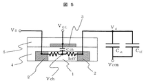
図5は、本発明の原理を説明するために、低温ポリシリコンを用いた代表的なアクティブマトリクス型液晶表示装置のひとつの画素の構造を模式的に示したものである。代表的な液晶表示装置の画素構造では画素容量(主に補助容量Cstと液晶容量CLCとで形成される)にチャージを蓄積し、番号1−5からなる画素TFTでこの画素容量への充電、保持を制御する。VGLにはこのTFTのON−OFFを制御するゲート線を接続し、Vsには画素電極に充電する電位を供給するソース電圧を印加する。なお、画素容量の反対側には共通電極Vcomに接続するものとする。 FIG. 5 schematically shows the structure of one pixel of a typical active matrix liquid crystal display device using low-temperature polysilicon in order to explain the principle of the present invention. Typical pixel capacitor in the pixel structure of the liquid crystal display device (mainly auxiliary capacitor C st and formed by the liquid crystal capacitance C LC) to accumulate charge, to the pixel capacitor in a pixel TFT formed of numbers 1-5 Control charging and holding. The V GL is connected a gate line for controlling the ON-OFF of the TFT, the Vs is applied a source voltage supplying a potential to charge the pixel electrode. Note that the opposite side of the pixel capacitor is connected to the common electrode Vcom .
画素TFTは、チャネル形成領域1とその両側にチャネル形成領域1を挟むように形成されたソース・ドレイン領域2、ゲート絶縁膜4を介してチャネル形成領域1の上に形成されたゲート電極3、およびこれらを覆う絶縁膜5から構成されている。一方のソース・ドレイン領域は画素と電気的に接続され、他方のソース・ドレイン領域は信号線電位VSを供給する部位へ電気的に接続されている。後述するが、説明の便宜上、ゲート電極3とチャネル形成領域1の間の容量を、ゲート電極−チャネル間容量Cchとする。また、当該画素TFTがOPEN状態すなわち電気的解放状態にある場合、チャネル−ソース・ドレイン領域間の抵抗値を、OFF抵抗、Roffと定義する。
The pixel TFT includes a
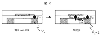
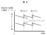
図6、図7、図8に上記の代表的な液晶表示装置における課題を模式的に示す。アクティブマトリクスディスプレイの場合、画素に書き込んだ後で、TFTをOPENにすることで画素電位を保持する。通常のデバイスではこの保持期間が60分の1秒が多いが、間欠駆動の場合はこの期間をどこまで伸ばせるかがポイントになる。
図6に示すように、TFT画素トランジスタをCLOSE状態すなわち電気的接続状態にして画素に電荷をチャージした後、TFTをOPEN状態にする。ここで、低温ポリシリコンTFTを用いて間欠駆動を実施すると、輝度変化が発生する問題が生じる。これは、OFF電流によるリーク電流で画素チャージが減少することに起因する。ポリシリコンは、アモルファスシリコンよりも結晶性が高いため、OFF特性が悪く、リークしやすい欠点がある。
つまり、図6のように、画素に電荷をチャージし、書き込みを行った後、一定時間放置すると、Roffを介してゲート電極−チャネル間容量Cch側へチャージが抜ける問題が生じる。チャージが抜けた結果、画素電位は、VaからVa−Δへと低下してしまう。問題は画素電極のチャージがリークすることにあり、最も基本的なモードは、この画素電極からソース電極に抜ける抵抗を介してリークするモードであり、これはデュアルゲート構造の採用やゲート線幅設計、半導体材料の精製で調整、設計可能である。但し、この画素からソースへのリークが十分に高抵抗を実現できたとしても、ゲート電極−チャネル間容量Cchへのリークが問題になる場合がある。これは、ゲート電極とポリシリコンのチャネル間に容量Cchが存在し、この充電電流が無視できないことに起因する。放置期間中にポリシリコン中にチャージが発生すると、このチャージによって徐々にゲート電極−チャネル間容量Cchを充電していく。概念的にはCchとRoffによるCR時定数で充電されるようなものである。
6, 7, and 8 schematically show the problems in the above-described typical liquid crystal display device. In the case of an active matrix display, the pixel potential is held by setting the TFT to OPEN after writing to the pixel. In a normal device, this holding period is 1 / 60th of a second, but in the case of intermittent driving, the point is how long this period can be extended.
As shown in FIG. 6, after the TFT pixel transistor is placed in the CLOSE state, that is, the electrical connection state, the pixel is charged with charge, and then the TFT is placed in the OPEN state. Here, when intermittent driving is performed using a low-temperature polysilicon TFT, there arises a problem that a luminance change occurs. This is because the pixel charge is reduced by the leakage current due to the OFF current. Since polysilicon has higher crystallinity than amorphous silicon, it has the disadvantage of poor OFF characteristics and easy leakage.
That is, as shown in FIG. 6, if a pixel is charged and written, and left for a certain period of time, there is a problem that the charge is released to the gate electrode-channel capacitance Cch side via R off . As a result of the loss of charge, the pixel potential decreases from Va to Va−Δ. The problem is that the charge on the pixel electrode leaks, and the most basic mode is a mode that leaks through a resistor that goes from the pixel electrode to the source electrode. This is a dual gate structure and gate line width design. It can be adjusted and designed by refining semiconductor materials. However, even if the leak from the pixel to the source can realize a sufficiently high resistance, the leak to the gate electrode-channel capacitance Cch may be a problem. This is because a capacitance Cch exists between the gate electrode and the polysilicon channel, and this charging current cannot be ignored. When charging occurs in the polysilicon during the leaving period, the gate electrode-channel capacitance Cch is gradually charged by this charging. Conceptually, it is charged with a CR time constant by C ch and R off .
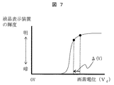
画素に電荷をチャージし、書き込みを行い、一定時間放置後にRoffを介してゲート電極−チャネル間容量Cch側へチャージが抜けてしまうと、図7に示すように、画素電位が低下した分、すなわちΔV分、液晶表示装置の輝度が低下する。アクティブマトリクス方式の表示装置では、図8のように周期的に書き込み動作を行うが、この画素電位の低下分、すなわちΔV分の輝度低下が表示のちらつき(フリッカ)となって認識されてしまう。 When the charge is discharged to the gate electrode-channel capacitor Cch side through R off after charging the pixel, writing, and leaving for a certain period of time, as shown in FIG. 7, the pixel potential decreases. That is, the brightness of the liquid crystal display device is reduced by ΔV. In the active matrix display device, the writing operation is periodically performed as shown in FIG. 8, but the decrease in pixel potential, that is, the decrease in luminance by ΔV is recognized as flickering of display.
ところで、代表的な液晶表示装置では、外部光による誤動作を防ぐため遮光層が形成される場合があるが、遮光層によりポリシリコンへの光照射を小さくすればこの時定数がさらに長くなることが判った。この時定数は1秒程度であった。間欠駆動の周波数が1Hz程度であれば、非常に大きな問題となるレベルである。補助容量Cstを含む画素容量が190fFに対し、ゲート容量が6fFと3%程度になる。この程度の容量でも、光学的な変化としては輝度の20%の変化となって現れるため、高精細な液晶表示装置では大きな問題となる。輝度変化が認識されないためには、輝度変化を1.4%以下に抑えなければならない。この輝度変化を抑える方法として、例えば、ゲート電極−チャネル間容量Cchを小さくすればこのCchへのリーク電流が小さくできるので、低減効果は期待できるが、ゲート電極−チャネル間容量Cchはゲート線幅の最小値、ゲート酸化膜の厚みに依存するため、極端に小さくすることは困難である。 By the way, in a typical liquid crystal display device, a light shielding layer may be formed to prevent malfunction due to external light. However, if the light irradiation to the polysilicon is reduced by the light shielding layer, this time constant may be further increased. understood. This time constant was about 1 second. If the frequency of intermittent driving is about 1 Hz, it is a level that poses a very big problem. To pixel capacitor comprising a storage capacitance C st is 190FF, the gate capacitance is about 6fF and 3%. Even at such a capacity, an optical change appears as a 20% change in luminance, which is a serious problem in a high-definition liquid crystal display device. In order for the luminance change not to be recognized, the luminance change must be suppressed to 1.4% or less. As a method of suppressing this change in luminance, for example, if the gate electrode-channel capacitance C ch is reduced, the leakage current to this C ch can be reduced, so that a reduction effect can be expected, but the gate electrode-channel capacitance C ch is Since it depends on the minimum value of the gate line width and the thickness of the gate oxide film, it is difficult to make it extremely small.
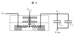
ゲート電極−チャネル間容量Cchを低減する手段として、上述の特許文献1のような容量結合のゲートを用いた例(図9)もあるが、表示装置の開口率を大きく低下させるデメリットがある。
As a means for reducing the gate electrode-channel capacitance Cch , there is an example (FIG. 9) using a capacitively coupled gate as described in
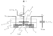
そこで本実施の形態における液晶表示装置は、図1に示すように、基板上に配置された画素に対し、第一の薄膜トランジスタを介して画素電位を供給するソース電源と、前記第一の薄膜トランジスタの導通と非導通を制御するゲート電源と、を有する表示装置であって、前記第一の薄膜トランジスタと前記ゲート電源の間に、前記第一の薄膜トランジスタと独立して制御可能な第二の薄膜トランジスタを備えることを特徴としている。 Therefore, as shown in FIG. 1, the liquid crystal display device according to the present embodiment includes a source power source that supplies a pixel potential to a pixel disposed on a substrate via a first thin film transistor, and the first thin film transistor. A display device having a gate power source that controls conduction and non-conduction, and a second thin film transistor that can be controlled independently of the first thin film transistor, between the first thin film transistor and the gate power source. It is characterized by that.
図1について、図5の説明と重複する部分を省略して説明する。図1に示すように、ゲート電源VGおよびTFT画素トランジスタを構成するゲート電極3の間に、TFT画素トランジスタとは独立して制御することが可能なTFTすなわち薄膜トランジスタA6が設けられている。画素への電荷のチャージ後、すなわち書き込み後、放置期間中にこの薄膜トランジスタA6のコントロールゲート電源CTL_VGに電圧を印加し、薄膜トランジスタA6をOPEN状態つまり電気的解放状態とすることにより、画素に保持された電荷が、チャネル−ソース・ドレイン領域間抵抗すなわちRoffを介してゲート電極−チャネル間容量Cchへ再充電されるのを抑制することができる。解放状態の容量では、その電荷は保持されるためである。これにより、駆動周波数を低減させることができ、たとえば1Hzの駆動周波数を実現した場合に、駆動電力は約60分の1にすることができる。また、画素にチャージされた電荷が保持期間中にリークしてしまうのを抑制できるため、一定時間放置後に画素電位が低下するのを防止することができ、液晶表示装置のちらつき、いわゆるフリッカ現象を低減することができる。これにより、低消費電力で、高精細な液晶表示装置を実現することが可能となる。 1 will be described by omitting the same parts as those in FIG. As shown in FIG. 1, between the gate electrode 3 forming the gate power supply V G and TFT pixel transistors, separate TFT i.e. thin film transistor A6 which can be controlled is provided with TFT pixel transistors. After charging of the charge to the pixel, that is, after the writing, the voltage is applied to the control gate power supply CTL_V G of the thin film transistor A6 during standing period, by a thin film transistor A6 and OPEN-states or electrically released state, is held by the pixel charges, the channel - the source and drain regions between resistor or gate via the R off electrode - can be prevented from being recharged to inter-channel capacitance C ch. This is because the charge is held in the released capacity. As a result, the drive frequency can be reduced. For example, when a drive frequency of 1 Hz is realized, the drive power can be reduced to about 1/60. In addition, since it is possible to suppress the leakage of the electric charge charged to the pixel during the holding period, it is possible to prevent the pixel potential from being lowered after being left for a certain period of time and to prevent flickering of the liquid crystal display device, so-called flicker phenomenon. Can be reduced. As a result, a high-definition liquid crystal display device with low power consumption can be realized.
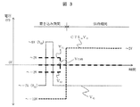
上記で説明した薄膜トランジスタA6、ゲート電源VG、対向電極電位すなわち共通電位Vcomの状態を表すタイムチャートを図3に示す。書き込み期間において、VGを−7V程度(VGL)から8V程度(VGH)へ昇圧し、画素に電荷をチャージする。このとき、薄膜トランジスタA6のコントロールゲート電源CTL_VGは−10V程度に保ち、薄膜トランジスタA6をCLOSE状態すなわち電気的接続状態としている。その後の保持期間において、薄膜トランジスタA6のコントロールゲート電源CTL_VGを5V程度まで昇圧し、薄膜トランジスタA6をOPEN状態すなわち電気的解放状態とし、画素に保持された電荷が、チャネル−ソース・ドレイン領域間抵抗すなわちRoffを介してゲート電極−チャネル間容量Cchへ再充電されるのを抑制する。 FIG. 3 shows a time chart showing the states of the thin film transistor A6, the gate power source V G , the counter electrode potential, that is, the common potential V com described above. In the writing period, V G is boosted from about −7 V (V GL ) to about 8 V (V GH ), and the pixel is charged. At this time, the control gate power supply CTL_V G of the thin film transistor A6 is maintained at about -10 V, and the thin film transistors A6 to the CLOSE state, that an electrical connection state. In a subsequent holding period, boosts the control gate power CTL_V G of the thin film transistor A6 to about 5V, a thin film transistor A6 and OPEN state, that electrically released state, the electric charges held in the pixel, the channel - between the source and drain regions resistor i.e. Recharging to the gate electrode-channel capacitance Cch via R off is suppressed.
本実施の形態における液晶表示装置においては、基板を、ガラス基板上に成膜されたアモルファスシリコン膜をレーザーアニールにより多結晶化して形成される低温ポリシリコン基板いわゆるLTPS−TFT(Low−Temperature−Poly−Silicon−TFT:低温ポリシリコンTFT)で製造しても良い。低温ポリシリコンはオフ電流が大きいため、この発明によるリーク電流を低減する効果が大きく、液晶表示装置のちらつき(フリッカ)を抑制することができる。 In the liquid crystal display device in this embodiment, a low-temperature polysilicon substrate so-called LTPS-TFT (Low-Temperature-Poly) formed by polycrystallizing an amorphous silicon film formed on a glass substrate by laser annealing. -Silicon-TFT: Low-temperature polysilicon TFT). Since low temperature polysilicon has a large off-state current, the effect of reducing the leakage current according to the present invention is great, and flickering of the liquid crystal display device can be suppressed.
また、本実施の形態における液晶表示装置は、第一の薄膜トランジスタを周期的に駆動させる間欠駆動型の表示装置に用いることができる。間欠駆動型の表示装置では、画素への電荷のチャージ後の放置期間に電荷が放電されやすいため本発明が、液晶表示装置のちらつき(フリッカ)防止には有効な解決手段となる。 The liquid crystal display device in this embodiment can be used for an intermittent drive type display device in which the first thin film transistor is periodically driven. In the intermittent drive type display device, since the charge is easily discharged during the leaving period after the charge is charged to the pixel, the present invention is an effective solution for preventing the flicker of the liquid crystal display device.
また、本実施の形態における液晶表示装置は、フリンジ電界を利用して液晶分子を駆動させるFFS(Fringe−Feild−Switching)方式や液晶分子を基板と平行な面内で回転させ、複屈折の変化で光をスイッチングするIPS(In−Plane−Switching)方式、初期状態で液晶を垂直に配向させ、電圧を印加させて液晶を倒すことにより変化する複屈折を利用して、透過状態(白)と非透過状態(黒)を表現するVA(Vertical−Alignment)方式、捻じれネマティック液晶いわゆるTN(Twisted−Nematic)方式等の液晶表示装置に用いることもできる。特に、FFS方式の液晶表示装置では、補助容量Cstが大きいため、本発明によるリーク電流が多少あってもフリッカ抑制に効果が高い。 In addition, the liquid crystal display device in this embodiment mode uses an FFS (Fringe-Feld-Switching) method in which liquid crystal molecules are driven using a fringe electric field, or the liquid crystal molecules are rotated in a plane parallel to the substrate to change birefringence. In an IPS (In-Plane-Switching) system for switching light in the initial state, the liquid crystal is oriented vertically in the initial state, and the birefringence that is changed by tilting the liquid crystal by applying a voltage is used to obtain a transmissive state (white). It can also be used for a liquid crystal display device such as a VA (Vertical-Alignment) method that expresses a non-transmissive state (black), a twisted nematic liquid crystal, or a so-called TN (Twisted-Nematic) method. In particular, in the FFS mode liquid crystal display device, since the auxiliary capacitance Cst is large, even if there is some leakage current according to the present invention, the effect of suppressing flicker is high.
また、本実施の形態における液晶表示装置は、画素を有機化合物を含む有機発光ダイオードで形成する、いわゆる有機EL(Organic−Electroluminescence)表示装置に適用することもできる。発光期間中の電流量変化が表示に影響を与えるため、有機ELでもフリッカの抑制、低消費電力化、高精細化に有効な手段となる。 Further, the liquid crystal display device in this embodiment can also be applied to a so-called organic EL (Organic-Electroluminescence) display device in which a pixel is formed using an organic light-emitting diode containing an organic compound. Since the change in the amount of current during the light emission period affects the display, organic EL is an effective means for suppressing flicker, reducing power consumption, and increasing definition.
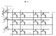
本発明における他の実施例を図2に示す。図2は、本実施例に係る液晶表示装置の一部回路構成を概略的に示している。この液晶表示装置は、基板上にマトリクス状に形成された画素に対し、それぞれの画素にTFT画素トランジスタを個別に有し、書き込み時以外はTFT画素トランジスタをOPEN状態すなわち電気的解放状態にして表示電荷を保持する、いわゆるアクティブマトリクス液晶表示装置となっている。画素と同様に基板上にマトリクス状に配置された複数のTFT画素トランジスタのゲート端子を一列毎に1つのゲート線に接続し、ゲート線の末端に電源供給部が接続されている。この電源供給部は、ゲート低電圧VGLとゲート高電圧VGHに接続され、どちらかに切り替える構造になっている。本実施の形態において、電源供給部はゲート低電圧VGLとゲート高電圧VGHのいずれかに切り替える構造の例を説明しているが、任意の電圧値が供給可能な電源すなわち複数の異なる電圧を印加できる電源を設けても良い。また、マトリクス状に配置された複数のTFT画素トランジスタのそれぞれのソース・ドレイン領域は、容量すなわち液晶容量および補助容量を介して1つの共通電位線に接続され、一列毎に纏めて対向電極電位すなわち共通電位Vcom供給部へ接続されている。本実施例では、上記のようにマトリクス状に配置された複数のTFT画素トランジスタのゲート端子を一列毎に纏めて接続する1つのゲート線および電源供給部との間に、ゲート線毎に薄膜トランジスタB7、薄膜トランジスタC8、薄膜トランジスタD9が設けられている。これにより、実施例1と同様に、画素への電荷のチャージ後すなわち書き込み後の保持期間に、これらの薄膜トランジスタB〜DをOPEN状態すなわち電気的解放状態とすることで、画素にチャージされた電荷が、保持期間中にチャネル−ソース・ドレイン領域間抵抗すなわちRoffを介してゲート電極−チャネル間容量Cchへ再充電されるのを抑制することができ、液晶表示装置の低消費電力化、高精細化が可能となる。本実施例では、1秒間の保持期間後も輝度変化が1%以下であり、良好な間欠駆動特性を得ることができた。 Another embodiment of the present invention is shown in FIG. FIG. 2 schematically shows a partial circuit configuration of the liquid crystal display device according to this embodiment. In this liquid crystal display device, for each pixel formed in a matrix on the substrate, each pixel has a TFT pixel transistor, and the TFT pixel transistor is displayed in an OPEN state, that is, an electrically open state, except during writing. This is a so-called active matrix liquid crystal display device that holds electric charges. Similarly to the pixels, the gate terminals of a plurality of TFT pixel transistors arranged in a matrix on the substrate are connected to one gate line for each column, and a power supply unit is connected to the end of the gate line. This power supply unit is connected to the gate low voltage V GL and the gate high voltage V GH and is switched to either one. In the present embodiment, an example of a structure in which the power supply unit is switched to either the gate low voltage V GL or the gate high voltage V GH is described. However, a power source that can supply an arbitrary voltage value, that is, a plurality of different voltages A power source capable of applying a voltage may be provided. The source / drain regions of the plurality of TFT pixel transistors arranged in a matrix are connected to one common potential line via a capacitor, that is, a liquid crystal capacitor and an auxiliary capacitor, and the counter electrode potential, It is connected to the common potential V com supply unit. In this embodiment, a thin film transistor B7 is provided for each gate line between one gate line and a power supply unit that collectively connect the gate terminals of a plurality of TFT pixel transistors arranged in a matrix as described above for each column. A thin film transistor C8 and a thin film transistor D9 are provided. Thus, as in the first embodiment, the charge charged in the pixel is obtained by setting the thin film transistors B to D in the OPEN state, that is, the electrical release state, after the charge is charged to the pixel, that is, after the writing. Can be prevented from being recharged to the gate electrode-channel capacitance Cch through the channel-source-drain region resistance, that is, R off during the holding period, and the power consumption of the liquid crystal display device can be reduced. High definition is possible. In this example, the luminance change was 1% or less even after the holding period of 1 second, and good intermittent drive characteristics could be obtained.
なお、本実施例における液晶表示装置において、実施例1と同様に、基板を、ガラス基板上に成膜されたアモルファスシリコン膜をレーザーアニールにより多結晶化して形成される低温ポリシリコン基板で製造しても良い。また、同様に間欠駆動型の表示装置に用いることもできる。さらには、FSS方式、IPS方式、VA方式、TN方式等の液晶表示装置や、いわゆる有機EL表示装置に採用しても良い。いずれの表示装置においても、低消費電力化、高精細化に有効な手段となる。 In the liquid crystal display device of this example, as in Example 1, the substrate was manufactured with a low-temperature polysilicon substrate formed by polycrystallizing an amorphous silicon film formed on a glass substrate by laser annealing. May be. Similarly, it can be used for an intermittent drive type display device. Furthermore, the present invention may be employed in a liquid crystal display device such as an FSS method, an IPS method, a VA method, or a TN method, or a so-called organic EL display device. Any display device is an effective means for reducing power consumption and increasing definition.
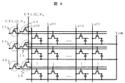
本発明に係る別の実施例を図4に示す。図4は、本実施例における液晶表示装置の一部回路構成を概略的に示している。スマートフォン等では、カラム反転駆動と呼ばれる、ソース線の奇数番目と偶数番目で書き込み信号の符号を変えてちらつきを抑制する駆動法が要求される場合がある。このカラム反転駆動は、極性が同じ画素毎にゲート線を束ねて結合させることで、保持特性を向上することができる。本実施例では図4のように、極性が同じ画素毎にゲート線を束ねて結合させることで、カラム反転駆動が可能となっている。また、本実施例においては、極性毎に束ねたゲート線毎にそれぞれ個別に、薄膜トランジスタE10、薄膜トランジスタF11、薄膜トランジスタG12、薄膜トランジスタH13、薄膜トランジスタI14、薄膜トランジスタJ15を設けることにより、実施例1と同様に、画素にチャージされた電荷が、保持期間中にチャネル−ソース・ドレイン領域間抵抗すなわちRoffを介してゲート電極−チャネル間容量Cchへ再充電されるのを抑制することができ、液晶表示装置の低消費電力化、高精細化が可能となる。 Another embodiment according to the present invention is shown in FIG. FIG. 4 schematically shows a partial circuit configuration of the liquid crystal display device according to this embodiment. Smartphones or the like may require a driving method called column inversion driving that suppresses flickering by changing the sign of a write signal between odd and even source lines. In this column inversion driving, the holding characteristics can be improved by bundling and coupling the gate lines for each pixel having the same polarity. In this embodiment, as shown in FIG. 4, column inversion driving is possible by bundling and connecting gate lines for each pixel having the same polarity. In the present embodiment, the thin film transistor E10, the thin film transistor F11, the thin film transistor G12, the thin film transistor H13, the thin film transistor I14, and the thin film transistor J15 are individually provided for each gate line bundled for each polarity. The charge charged to the pixel can be prevented from being recharged to the gate electrode-channel capacitor Cch via the channel-source-drain region resistance, that is, R off during the holding period, and the liquid crystal display device Low power consumption and high definition can be achieved.
画素をマトリクス状に配置したアクティブマトリクス方式の表示装置においては、複数の画素間でリークチャージの移動が発生する場合がある。これは個々の画素の電荷のチャージ量が大きく異なると電荷の移動が起きやすくなるためである。そこで、本実施例のようにプラス極性とマイナス極性を別々に束ねた構成とすることで、各画素における電荷の保持特性が改善される。但し、ゲート線が各行に2本づつになるため、開口率が低下する点ではデメリットとなる。 In an active matrix display device in which pixels are arranged in a matrix, leakage charge may move between a plurality of pixels. This is because the movement of charges is likely to occur when the charge amounts of the charges of individual pixels differ greatly. Therefore, by using a configuration in which the positive polarity and the negative polarity are separately bundled as in this embodiment, the charge retention characteristics in each pixel are improved. However, since there are two gate lines in each row, there is a demerit in that the aperture ratio decreases.
なお、本実施例における液晶表示装置において、実施例1と同様に、基板を、ガラス基板上に成膜されたアモルファスシリコン膜をレーザーアニールにより多結晶化して形成される低温ポリシリコン基板で製造しても良い。また、同様に間欠駆動型の表示装置に用いることもできる。さらには、FSS方式、IPS方式、VA方式、TN方式等の液晶表示装置や、いわゆる有機EL表示装置に採用しても良い。いずれの表示装置においても、低消費電力化、高精細化に有効な手段となる。 In the liquid crystal display device of this example, as in Example 1, the substrate was manufactured with a low-temperature polysilicon substrate formed by polycrystallizing an amorphous silicon film formed on a glass substrate by laser annealing. May be. Similarly, it can be used for an intermittent drive type display device. Furthermore, the present invention may be employed in a liquid crystal display device such as an FSS method, an IPS method, a VA method, or a TN method, or a so-called organic EL display device. Any display device is an effective means for reducing power consumption and increasing definition.
以上の各実施例においては、画素に電荷をチャージ後、すなわち書き込み後の保持期間中にゲート線すなわちゲート電源をOPENすなわち電気的解放状態にすることで、ゲート容量の変動を抑える例について説明しているが、原理的にはソース線においても同様の効果があり、保持期間中にソース線もOPEN状態にした場合は、なお一層の効果を得ることができる。 In each of the above embodiments, an example is described in which the gate line, that is, the gate power supply is set to OPEN, that is, in an electrically released state after the pixel is charged, that is, during the holding period after writing, to suppress the variation in the gate capacitance. However, in principle, the same effect can be obtained for the source line, and if the source line is also in the OPEN state during the holding period, a further effect can be obtained.
また、以上の各実施形態においては、開示例として液晶表示装置の場合を主に例示したが、その他の適用例として、有機EL表示装置、その他の自発光型表示装置、あるいは電気泳動素子等を有する電子ペーパー型表示装置等、あらゆるフラットパネル型の表示装置が挙げられる。また、中小型から大型まで、特に限定することなく適用が可能であることは言うまでもない。 In each of the above embodiments, the case of a liquid crystal display device is mainly exemplified as a disclosure example. However, as other application examples, an organic EL display device, other self-luminous display devices, an electrophoretic element, and the like Any flat panel display device such as an electronic paper display device is included. Moreover, it cannot be overemphasized that it can apply, without specifically limiting from a small size to a large size.
1…チャネル形成領域、2…ソース・ドレイン領域、3…ゲート電極、4…ゲート絶縁膜、5…絶縁膜、6…薄膜トランジスタA、7…薄膜トランジスタB、8…薄膜トランジスタC、9…薄膜トランジスタD、10…薄膜トランジスタE、11…薄膜トランジスタF、12…薄膜トランジスタG、13…薄膜トランジスタH、14…薄膜トランジスタI、15…薄膜トランジスタJ。
DESCRIPTION OF
Claims (16)
前記第一の薄膜トランジスタの導通と非導通を制御するゲート電源と、を有する表示装置であって、
前記第一の薄膜トランジスタと前記ゲート電源の間に、前記第一の薄膜トランジスタと独立して制御可能な第二の薄膜トランジスタを備えることを特徴とする表示装置。 A source power source for supplying a pixel potential to the pixels disposed on the substrate via the first thin film transistor;
A gate power source for controlling conduction and non-conduction of the first thin film transistor,
A display device comprising a second thin film transistor that can be controlled independently of the first thin film transistor between the first thin film transistor and the gate power supply.
前記第一の薄膜トランジスタの導通と非導通を制御するゲート電源群と、を有する表示装置であって、
前記第一の薄膜トランジスタと前記ゲート電源の間に、前記第一の薄膜トランジスタと独立して制御可能な第二の薄膜トランジスタを備えることを特徴とする表示装置。 A source power supply group for supplying a pixel potential to the plurality of pixels arranged in a matrix on the substrate via the first thin film transistor;
A gate power supply group for controlling conduction and non-conduction of the first thin film transistor,
A display device comprising a second thin film transistor that can be controlled independently of the first thin film transistor between the first thin film transistor and the gate power supply.
前記基板上の前記第一の画素群と異なる領域に、一定の間隔を空けて画素を配置した第二の画素群に対し、複数の第二の薄膜トランジスタを介して前記画素電位と異なる極性の電位を供給する第二のソース電源群と、
前記第一の薄膜トランジスタの導通と非導通を制御する第一のゲート電源群と、
前記第二の薄膜トランジスタの導通と非導通を制御する第二のゲート電源群と、を有する表示装置であって、
前記第一の薄膜トランジスタと前記第一のゲート電源群の間に、独立して制御可能な第三の薄膜トランジスタと、
前記第二の薄膜トランジスタと前記第二のゲート電源群の間に、独立して制御可能な第四の薄膜トランジスタと、を備えることを特徴とする表示装置。 A first source power supply group for supplying a pixel potential via a plurality of first thin film transistors to a first pixel group in which pixels are arranged at a predetermined interval on a substrate;
A potential having a polarity different from that of the pixel potential via a plurality of second thin film transistors with respect to a second pixel group in which pixels are arranged at a predetermined interval in a region different from the first pixel group on the substrate. A second source power supply group,
A first gate power supply group for controlling conduction and non-conduction of the first thin film transistor;
A second gate power supply group for controlling conduction and non-conduction of the second thin film transistor,
A third thin film transistor that can be independently controlled between the first thin film transistor and the first gate power source group;
A display device comprising: a fourth thin film transistor that can be independently controlled between the second thin film transistor and the second gate power supply group.
Priority Applications (3)
| Application Number | Priority Date | Filing Date | Title |
|---|---|---|---|
| JP2013254207A JP2015114376A (en) | 2013-12-09 | 2013-12-09 | Display device |
| US14/564,142 US9666150B2 (en) | 2013-12-09 | 2014-12-09 | Display device |
| US15/496,308 US9905156B2 (en) | 2013-12-09 | 2017-04-25 | Display device |
Applications Claiming Priority (1)
| Application Number | Priority Date | Filing Date | Title |
|---|---|---|---|
| JP2013254207A JP2015114376A (en) | 2013-12-09 | 2013-12-09 | Display device |
Publications (1)
| Publication Number | Publication Date |
|---|---|
| JP2015114376A true JP2015114376A (en) | 2015-06-22 |
Family
ID=53271789
Family Applications (1)
| Application Number | Title | Priority Date | Filing Date |
|---|---|---|---|
| JP2013254207A Pending JP2015114376A (en) | 2013-12-09 | 2013-12-09 | Display device |
Country Status (2)
| Country | Link |
|---|---|
| US (2) | US9666150B2 (en) |
| JP (1) | JP2015114376A (en) |
Families Citing this family (2)
| Publication number | Priority date | Publication date | Assignee | Title |
|---|---|---|---|---|
| KR102597024B1 (en) | 2015-11-23 | 2023-11-02 | 삼성디스플레이 주식회사 | Organic light emitting display |
| JP6753450B2 (en) * | 2018-11-12 | 2020-09-09 | セイコーエプソン株式会社 | Substrates for electro-optical devices, electro-optic devices, electronic devices |
Citations (6)
| Publication number | Priority date | Publication date | Assignee | Title |
|---|---|---|---|---|
| JPH07181927A (en) * | 1993-12-24 | 1995-07-21 | Sharp Corp | Image display device |
| US6124840A (en) * | 1997-04-07 | 2000-09-26 | Hyundai Electronics Industries Co., Ltd. | Low power gate driver circuit for thin film transistor-liquid crystal display (TFT-LCD) using electric charge recycling technique |
| JP2002358051A (en) * | 2001-05-31 | 2002-12-13 | Matsushita Electric Ind Co Ltd | Driving method for liquid crystal display device and liquid crystal display device |
| JP2010266849A (en) * | 2009-04-14 | 2010-11-25 | Nec Lcd Technologies Ltd | Scanning line driving circuit, display, and scanning line driving method |
| JP2011048225A (en) * | 2009-08-28 | 2011-03-10 | Sony Corp | Liquid crystal display device |
| WO2012042566A1 (en) * | 2010-09-29 | 2012-04-05 | パナソニック株式会社 | Thin-film semiconductor device for display device, method for producing thin-film semiconductor device for display device, el display panel and el display device |
Family Cites Families (6)
| Publication number | Priority date | Publication date | Assignee | Title |
|---|---|---|---|---|
| TW277129B (en) | 1993-12-24 | 1996-06-01 | Sharp Kk | |
| JP3402909B2 (en) | 1996-03-12 | 2003-05-06 | アルプス電気株式会社 | Thin film transistor device and liquid crystal display device |
| KR100686334B1 (en) * | 2003-11-14 | 2007-02-22 | 삼성에스디아이 주식회사 | Pixel circuit in display device and Driving method thereof |
| JP2006184577A (en) * | 2004-12-27 | 2006-07-13 | Toshiba Matsushita Display Technology Co Ltd | Display device, array substrate, and method of manufacturing display device |
| WO2011007677A1 (en) * | 2009-07-17 | 2011-01-20 | Semiconductor Energy Laboratory Co., Ltd. | Semiconductor device and method for manufacturing the same |
| US8718224B2 (en) * | 2011-08-05 | 2014-05-06 | Semiconductor Energy Laboratory Co., Ltd. | Pulse signal output circuit and shift register |
-
2013
- 2013-12-09 JP JP2013254207A patent/JP2015114376A/en active Pending
-
2014
- 2014-12-09 US US14/564,142 patent/US9666150B2/en active Active
-
2017
- 2017-04-25 US US15/496,308 patent/US9905156B2/en active Active
Patent Citations (6)
| Publication number | Priority date | Publication date | Assignee | Title |
|---|---|---|---|---|
| JPH07181927A (en) * | 1993-12-24 | 1995-07-21 | Sharp Corp | Image display device |
| US6124840A (en) * | 1997-04-07 | 2000-09-26 | Hyundai Electronics Industries Co., Ltd. | Low power gate driver circuit for thin film transistor-liquid crystal display (TFT-LCD) using electric charge recycling technique |
| JP2002358051A (en) * | 2001-05-31 | 2002-12-13 | Matsushita Electric Ind Co Ltd | Driving method for liquid crystal display device and liquid crystal display device |
| JP2010266849A (en) * | 2009-04-14 | 2010-11-25 | Nec Lcd Technologies Ltd | Scanning line driving circuit, display, and scanning line driving method |
| JP2011048225A (en) * | 2009-08-28 | 2011-03-10 | Sony Corp | Liquid crystal display device |
| WO2012042566A1 (en) * | 2010-09-29 | 2012-04-05 | パナソニック株式会社 | Thin-film semiconductor device for display device, method for producing thin-film semiconductor device for display device, el display panel and el display device |
Also Published As
| Publication number | Publication date |
|---|---|
| US9666150B2 (en) | 2017-05-30 |
| US20170229058A1 (en) | 2017-08-10 |
| US20150161966A1 (en) | 2015-06-11 |
| US9905156B2 (en) | 2018-02-27 |
Similar Documents
| Publication | Publication Date | Title |
|---|---|---|
| US9202441B2 (en) | Electronic apparatus system for dynamically adjusting display mode and drive method of display panel | |
| JP5351974B2 (en) | Display device | |
| JP5452616B2 (en) | Pixel circuit and display device | |
| JP5346381B2 (en) | Pixel circuit and display device | |
| JP6334114B2 (en) | Display device | |
| US20150161946A1 (en) | Display systems | |
| JP5351973B2 (en) | Pixel circuit and display device | |
| US10636373B2 (en) | Pixel circuit, memory circuit, display panel and driving method | |
| US9530384B2 (en) | Display device that compensates for changes in driving frequency and drive method thereof | |
| JP5342657B2 (en) | Display device | |
| US20160254276A1 (en) | Display device | |
| US10204590B2 (en) | Pixel unit, driving method thereof, array substrate, and display device | |
| US20160307527A1 (en) | Liquid crystal display device and method of driving the same | |
| US20130147783A1 (en) | Pixel circuit and display device | |
| WO2012056804A1 (en) | Display device | |
| US9412324B2 (en) | Drive device and display device | |
| US9905156B2 (en) | Display device | |
| US20120313915A1 (en) | Thin-film transistor (tft) array and liquid crystal display (lcd) panel thereof | |
| US8766888B2 (en) | In plane switching mode liquid crystal display device | |
| US9355606B2 (en) | Liquid crystal display device and liquid crystal display device driving method | |
| US20090201437A1 (en) | Liquid crystal display device and method of driving the same | |
| US10127881B2 (en) | Display driving circuit, display device and driving method thereof | |
| CN107422558B (en) | Liquid crystal panel and driving method thereof | |
| US20190088222A1 (en) | Liquid crystal display device | |
| KR20070002533A (en) | Liquid crystal display panel |
Legal Events
| Date | Code | Title | Description |
|---|---|---|---|
| A621 | Written request for application examination |
Free format text: JAPANESE INTERMEDIATE CODE: A621 Effective date: 20160909 |
|
| A977 | Report on retrieval |
Free format text: JAPANESE INTERMEDIATE CODE: A971007 Effective date: 20170725 |
|
| A131 | Notification of reasons for refusal |
Free format text: JAPANESE INTERMEDIATE CODE: A131 Effective date: 20170815 |
|
| A02 | Decision of refusal |
Free format text: JAPANESE INTERMEDIATE CODE: A02 Effective date: 20180306 |