JP2015080601A - Pulse wave sensor and biological information measuring device using the same - Google Patents
Pulse wave sensor and biological information measuring device using the same Download PDFInfo
- Publication number
- JP2015080601A JP2015080601A JP2013219891A JP2013219891A JP2015080601A JP 2015080601 A JP2015080601 A JP 2015080601A JP 2013219891 A JP2013219891 A JP 2013219891A JP 2013219891 A JP2013219891 A JP 2013219891A JP 2015080601 A JP2015080601 A JP 2015080601A
- Authority
- JP
- Japan
- Prior art keywords
- pulse wave
- light emitting
- light
- opening
- wave sensor
- Prior art date
- Legal status (The legal status is an assumption and is not a legal conclusion. Google has not performed a legal analysis and makes no representation as to the accuracy of the status listed.)
- Withdrawn
Links
- 239000000758 substrate Substances 0.000 claims abstract description 83
- 238000001514 detection method Methods 0.000 claims abstract description 70
- 238000005259 measurement Methods 0.000 claims description 46
- 229910000679 solder Inorganic materials 0.000 claims description 5
- 210000004204 blood vessel Anatomy 0.000 description 13
- 238000006243 chemical reaction Methods 0.000 description 11
- 238000007747 plating Methods 0.000 description 9
- 210000000707 wrist Anatomy 0.000 description 9
- 239000008280 blood Substances 0.000 description 8
- 210000004369 blood Anatomy 0.000 description 8
- 230000006870 function Effects 0.000 description 8
- 238000013500 data storage Methods 0.000 description 7
- 210000001519 tissue Anatomy 0.000 description 7
- 239000010949 copper Substances 0.000 description 6
- 238000000034 method Methods 0.000 description 6
- 239000002245 particle Substances 0.000 description 6
- PXHVJJICTQNCMI-UHFFFAOYSA-N Nickel Chemical compound [Ni] PXHVJJICTQNCMI-UHFFFAOYSA-N 0.000 description 5
- 238000010586 diagram Methods 0.000 description 4
- RYGMFSIKBFXOCR-UHFFFAOYSA-N Copper Chemical compound [Cu] RYGMFSIKBFXOCR-UHFFFAOYSA-N 0.000 description 3
- 229910052802 copper Inorganic materials 0.000 description 3
- 230000003287 optical effect Effects 0.000 description 3
- 239000011347 resin Substances 0.000 description 3
- 229920005989 resin Polymers 0.000 description 3
- 210000000709 aorta Anatomy 0.000 description 2
- 210000001367 artery Anatomy 0.000 description 2
- 230000008602 contraction Effects 0.000 description 2
- 210000000624 ear auricle Anatomy 0.000 description 2
- 239000011521 glass Substances 0.000 description 2
- 238000009413 insulation Methods 0.000 description 2
- 238000004519 manufacturing process Methods 0.000 description 2
- 239000000463 material Substances 0.000 description 2
- 229910052759 nickel Inorganic materials 0.000 description 2
- 230000002093 peripheral effect Effects 0.000 description 2
- 229910000881 Cu alloy Inorganic materials 0.000 description 1
- 239000004593 Epoxy Substances 0.000 description 1
- NIXOWILDQLNWCW-UHFFFAOYSA-N acrylic acid group Chemical group C(C=C)(=O)O NIXOWILDQLNWCW-UHFFFAOYSA-N 0.000 description 1
- 230000000903 blocking effect Effects 0.000 description 1
- 238000001816 cooling Methods 0.000 description 1
- 239000006071 cream Substances 0.000 description 1
- 210000004207 dermis Anatomy 0.000 description 1
- 238000007772 electroless plating Methods 0.000 description 1
- 210000002615 epidermis Anatomy 0.000 description 1
- 210000003811 finger Anatomy 0.000 description 1
- PCHJSUWPFVWCPO-UHFFFAOYSA-N gold Chemical compound [Au] PCHJSUWPFVWCPO-UHFFFAOYSA-N 0.000 description 1
- 229910052737 gold Inorganic materials 0.000 description 1
- 239000010931 gold Substances 0.000 description 1
- 230000001678 irradiating effect Effects 0.000 description 1
- 210000005240 left ventricle Anatomy 0.000 description 1
- 239000002184 metal Substances 0.000 description 1
- 229910052751 metal Inorganic materials 0.000 description 1
- 238000000465 moulding Methods 0.000 description 1
- 230000000149 penetrating effect Effects 0.000 description 1
- 230000010349 pulsation Effects 0.000 description 1
- 230000000717 retained effect Effects 0.000 description 1
- 238000005476 soldering Methods 0.000 description 1
- JBQYATWDVHIOAR-UHFFFAOYSA-N tellanylidenegermanium Chemical compound [Te]=[Ge] JBQYATWDVHIOAR-UHFFFAOYSA-N 0.000 description 1
- 229920001187 thermosetting polymer Polymers 0.000 description 1
- 238000002834 transmittance Methods 0.000 description 1
- 230000002792 vascular Effects 0.000 description 1
- 238000004804 winding Methods 0.000 description 1
Images


Classifications
-
- A—HUMAN NECESSITIES
- A61—MEDICAL OR VETERINARY SCIENCE; HYGIENE
- A61B—DIAGNOSIS; SURGERY; IDENTIFICATION
- A61B5/00—Measuring for diagnostic purposes; Identification of persons
- A61B5/68—Arrangements of detecting, measuring or recording means, e.g. sensors, in relation to patient
- A61B5/6801—Arrangements of detecting, measuring or recording means, e.g. sensors, in relation to patient specially adapted to be attached to or worn on the body surface
- A61B5/6813—Specially adapted to be attached to a specific body part
- A61B5/6824—Arm or wrist
-
- A—HUMAN NECESSITIES
- A61—MEDICAL OR VETERINARY SCIENCE; HYGIENE
- A61B—DIAGNOSIS; SURGERY; IDENTIFICATION
- A61B5/00—Measuring for diagnostic purposes; Identification of persons
- A61B5/68—Arrangements of detecting, measuring or recording means, e.g. sensors, in relation to patient
- A61B5/6801—Arrangements of detecting, measuring or recording means, e.g. sensors, in relation to patient specially adapted to be attached to or worn on the body surface
- A61B5/6802—Sensor mounted on worn items
- A61B5/681—Wristwatch-type devices
-
- A—HUMAN NECESSITIES
- A61—MEDICAL OR VETERINARY SCIENCE; HYGIENE
- A61B—DIAGNOSIS; SURGERY; IDENTIFICATION
- A61B5/00—Measuring for diagnostic purposes; Identification of persons
- A61B5/0059—Measuring for diagnostic purposes; Identification of persons using light, e.g. diagnosis by transillumination, diascopy, fluorescence
-
- A—HUMAN NECESSITIES
- A61—MEDICAL OR VETERINARY SCIENCE; HYGIENE
- A61B—DIAGNOSIS; SURGERY; IDENTIFICATION
- A61B5/00—Measuring for diagnostic purposes; Identification of persons
- A61B5/02—Detecting, measuring or recording pulse, heart rate, blood pressure or blood flow; Combined pulse/heart-rate/blood pressure determination; Evaluating a cardiovascular condition not otherwise provided for, e.g. using combinations of techniques provided for in this group with electrocardiography or electroauscultation; Heart catheters for measuring blood pressure
- A61B5/024—Detecting, measuring or recording pulse rate or heart rate
- A61B5/02416—Detecting, measuring or recording pulse rate or heart rate using photoplethysmograph signals, e.g. generated by infrared radiation
- A61B5/02427—Details of sensor
-
- A—HUMAN NECESSITIES
- A61—MEDICAL OR VETERINARY SCIENCE; HYGIENE
- A61B—DIAGNOSIS; SURGERY; IDENTIFICATION
- A61B5/00—Measuring for diagnostic purposes; Identification of persons
- A61B5/02—Detecting, measuring or recording pulse, heart rate, blood pressure or blood flow; Combined pulse/heart-rate/blood pressure determination; Evaluating a cardiovascular condition not otherwise provided for, e.g. using combinations of techniques provided for in this group with electrocardiography or electroauscultation; Heart catheters for measuring blood pressure
- A61B5/024—Detecting, measuring or recording pulse rate or heart rate
- A61B5/02444—Details of sensor
Landscapes
- Health & Medical Sciences (AREA)
- Life Sciences & Earth Sciences (AREA)
- Biomedical Technology (AREA)
- Heart & Thoracic Surgery (AREA)
- Veterinary Medicine (AREA)
- Biophysics (AREA)
- Pathology (AREA)
- Engineering & Computer Science (AREA)
- Public Health (AREA)
- Physics & Mathematics (AREA)
- Medical Informatics (AREA)
- Molecular Biology (AREA)
- Surgery (AREA)
- Animal Behavior & Ethology (AREA)
- General Health & Medical Sciences (AREA)
- Cardiology (AREA)
- Physiology (AREA)
- Measuring Pulse, Heart Rate, Blood Pressure Or Blood Flow (AREA)
Abstract
Description
本発明は、被験者の脈波を光学的に測定する脈波センサー、及び、そのような脈波センサーを用いた生体情報測定装置等に関する。 The present invention relates to a pulse wave sensor that optically measures a pulse wave of a subject, a biological information measuring device using such a pulse wave sensor, and the like.
心臓が収縮し、左心室から血液が大動脈に駆出されると大動脈の内圧に変化が生じ、さらに、その内圧変化が抹消動脈に伝達される。このような心臓の血液駆出に伴う血管の拍動(脈拍)の変化を波形として捉えたものを脈波という。心臓の動きそのものではなく、末梢血管系の容積変化を測定することによって、間接的に心電図と同様の意味を持つ情報が得られると言われている。 When the heart contracts and blood is ejected from the left ventricle into the aorta, the internal pressure of the aorta changes, and the change in internal pressure is transmitted to the peripheral artery. Such a change in blood vessel pulsation (pulse) accompanying the ejection of blood from the heart is called a pulse wave. It is said that information having the same meaning as an electrocardiogram can be obtained indirectly by measuring the volume change of the peripheral vascular system, not the heart movement itself.
光電変換を利用した脈波測定においては、被験者の手首や手指や耳朶等を測定部位として、発光素子と受光素子とを有する脈波センサーが測定部位に装着される。その状態で、血液に吸収され易い波長を有する光が、発光素子から測定部位に向けて照射され、血管内を流れる血液による減衰量の変動を受けて、生体組織によって反射された反射光又は生体組織を透過した透過光が受光素子に入射する。さらに、受光素子が、入射した光を光電変換することにより、電気信号である脈波測定信号を生成する。 In pulse wave measurement using photoelectric conversion, a pulse wave sensor having a light emitting element and a light receiving element is mounted on the measurement site with the subject's wrist, fingers, earlobe, or the like as the measurement site. In this state, light having a wavelength that is easily absorbed by blood is irradiated from the light emitting element toward the measurement site, is subjected to fluctuations in attenuation due to blood flowing in the blood vessel, and is reflected by living tissue or living body The transmitted light that has passed through the tissue enters the light receiving element. Further, the light receiving element photoelectrically converts the incident light to generate a pulse wave measurement signal that is an electrical signal.
ここで、発光素子から照射されて生体組織を介さずに受光素子に入射する光の強度が大きい場合には、脈波測定信号のSN比が低下して脈波測定を正確に行うことができなくなるという問題がある。従って、脈波測定の精度を向上させるためには、発光素子から受光素子に直接的に入射する光を遮断する必要がある。 Here, when the intensity of light irradiated from the light emitting element and incident on the light receiving element without passing through the living tissue is high, the S / N ratio of the pulse wave measurement signal is lowered and the pulse wave measurement can be performed accurately. There is a problem of disappearing. Therefore, in order to improve the accuracy of pulse wave measurement, it is necessary to block light that directly enters the light receiving element from the light emitting element.
関連する技術として、特許文献1には、被験者の運動時における脈波を精度良く測定することを目的とする脈波センサーが開示されている。この脈波センサーは、発光部から生体に光を照射して生体内を透過した光の強度を受光部で検出することにより脈波データを取得する光センサー部を備えた脈波センサーであって、光センサー部が、枡形状のケースと、該ケースを発光部が載置される第1領域と受光部が載置される第2領域とに分割する遮光壁とを有する構成とされている。
As a related technique,
しかしながら、特許文献1においては、光センサー部が、枡形状のケースと、該ケースを発光部が載置される第1領域と受光部が載置される第2領域とに分割する遮光壁とを有することにより、脈波センサーの厚さを薄くすることができなかった。また、枡形状のケース及び遮光壁を設けるために、脈波センサーのコストが上昇していた。そこで、本発明の1つの目的は、脈波センサーの厚さを薄くすると共に、脈波センサーのコストダウンを図ることである。また、本発明の他の目的は、そのような脈波センサーを用いた生体情報測定装置等を提供することである。
However, in
以上の課題を解決するため、本発明の1つの観点に係る脈波センサーは、互いに対向する第1の主面及び第2の主面を有し、該第1及び第2の主面を貫通する第1の開口部及び第2の開口部が形成され、少なくとも第1の開口部と第2の開口部との間に非透明な部分を含むセンサー基板と、第1の主面に実装され、第1の開口部内に挿入された発光面を有する発光素子と、第1の主面に実装され、発光素子の発光面から射出されて第2の主面側において反射された光が第2の開口部を通過して入射する検出面を有する反射光検出素子とを具備する。 In order to solve the above problems, a pulse wave sensor according to one aspect of the present invention has a first main surface and a second main surface that face each other, and penetrates the first and second main surfaces. And a sensor substrate including at least a non-transparent portion between the first opening and the second opening, and mounted on the first main surface. A light emitting element having a light emitting surface inserted into the first opening, and light that is mounted on the first main surface, emitted from the light emitting surface of the light emitting element, and reflected on the second main surface side is second. And a reflected light detection element having a detection surface incident through the opening.
本発明の1つの観点によれば、センサー基板が、少なくとも第1の開口部と第2の開口部との間に非透明な部分を含んでいるので、この非透明な部分が、発光素子と反射光検出素子との間を遮光する遮光壁として機能する。従って、発光素子と反射光検出素子との間を遮光するために特別な遮光部品をセンサー基板に設ける必要がないので、脈波センサーの厚さを薄くすると共に、脈波センサーのコストダウンを図ることができる。 According to one aspect of the present invention, the sensor substrate includes a non-transparent portion at least between the first opening and the second opening. It functions as a light shielding wall that shields light from the reflected light detection element. Therefore, it is not necessary to provide a special light shielding component on the sensor substrate to shield between the light emitting element and the reflected light detecting element, so that the thickness of the pulse wave sensor is reduced and the cost of the pulse wave sensor is reduced. be able to.
ここで、センサー基板が、発光素子の発光面からセンサー基板を介して反射光検出素子の検出面に入射する光によって反射光検出素子が反応しない程度の非透明性を有することが望ましい。その場合には、発光素子の発光面からセンサー基板を介して反射光検出素子の検出面に入射する光によって脈波測定信号のSN比が劣化するおそれがなくなる。 Here, it is desirable that the sensor substrate has non-transparency such that the reflected light detection element does not react with light incident on the detection surface of the reflected light detection element through the sensor substrate from the light emitting surface of the light emitting element. In that case, there is no possibility that the SN ratio of the pulse wave measurement signal is deteriorated by light incident on the detection surface of the reflected light detection element through the sensor substrate from the light emitting surface of the light emitting element.
以上において、センサー基板が、第1又は第2の開口部の側面に形成された反射層を含むようにしても良い。反射層が、発光素子から射出される光を反射することにより、発光素子の発光面からセンサー基板を介して反射光検出素子の検出面に入射する光を減少させることができる。 In the above, the sensor substrate may include a reflective layer formed on the side surface of the first or second opening. By reflecting the light emitted from the light emitting element, the reflection layer can reduce the light incident on the detection surface of the reflected light detection element through the sensor substrate from the light emitting surface of the light emitting element.
あるいは、センサー基板が、第1又は第2の開口部の側面に形成されたメッキ層を含むようにしても良い。メッキ層が、発光素子から射出される光を反射又は減衰させることにより、発光素子の発光面からセンサー基板を介して反射光検出素子の検出面に入射する光を減少させることができる。その場合には、スルーホールを有する一般的な両面配線基板の製造工程を利用して、センサー基板の第1の開口部又は第2の開口部の側面にメッキ層を形成することができる。 Alternatively, the sensor substrate may include a plating layer formed on the side surface of the first or second opening. The plating layer reflects or attenuates the light emitted from the light emitting element, whereby the light incident on the detection surface of the reflected light detection element from the light emitting surface of the light emitting element through the sensor substrate can be reduced. In that case, a plating layer can be formed on the side surface of the first opening or the second opening of the sensor substrate by using a manufacturing process of a general double-sided wiring board having a through hole.
発光素子の発光面は、センサー基板の第2の主面よりも外側に突出しないことが望ましい。その場合には、発光素子の発光面から射出される光の広がりが抑制されるので、生体組織以外の物体によって反射されて反射光検出素子の検出面に入射する光の量を低減することができる。 It is desirable that the light emitting surface of the light emitting element does not protrude outward from the second main surface of the sensor substrate. In that case, since the spread of the light emitted from the light emitting surface of the light emitting element is suppressed, the amount of light reflected by an object other than the living tissue and incident on the detection surface of the reflected light detecting element can be reduced. it can.
また、発光素子が、センサー基板の第2の主面よりも外側に突出するように発光面上に配置されたレンズ部をさらに有しても良い。レンズ部を設けることにより、発光素子の発光面から射出される光を収束させると共に、レンズ部をセンサー基板の第2の主面よりも外側に突出させることにより、レンズ部を設けるためにセンサー基板を厚くする必要がなくなる。 The light emitting element may further include a lens portion arranged on the light emitting surface so as to protrude outward from the second main surface of the sensor substrate. By providing the lens portion, the light emitted from the light emitting surface of the light emitting element is converged, and the lens portion is projected outward from the second main surface of the sensor substrate, thereby providing the sensor substrate. There is no need to increase the thickness.
発光素子及び反射光検出素子の複数の端子は、センサー基板の第1の主面に形成された複数の電極に、半田によってそれぞれ接続されても良い。その場合には、一般的な表面実装技術を用いることができる。 The plurality of terminals of the light emitting element and the reflected light detecting element may be connected to the plurality of electrodes formed on the first main surface of the sensor substrate by soldering. In that case, a general surface mounting technique can be used.
あるいは、反射光検出素子が、ACF(異方性導電フィルム)又はACP(異方性導電ペースト)を用いて、センサー基板の第1の主面に実装されても良い。その場合には、横方向に並ぶ端子間の間隔が狭くても、端子間の短絡を生じることなく反射光検出素子を実装することができる。 Alternatively, the reflected light detection element may be mounted on the first main surface of the sensor substrate using ACF (anisotropic conductive film) or ACP (anisotropic conductive paste). In that case, the reflected light detection element can be mounted without causing a short circuit between the terminals even if the interval between the terminals arranged in the horizontal direction is narrow.
また、第2の開口部の周囲において、反射光検出素子とセンサー基板の第1の主面との間に、ACF(異方性導電フィルム)、ACP(異方性導電ペースト)、NCF(非導電性フィルム)、又は、NCP(非導電性ペースト)が充填されても良い。その場合には、反射光検出素子とセンサー基板の第1の主面との間の隙間が塞がれるので、センサー基板の第1の主面側から反射光検出素子の検出面に漏れこむ光を遮断して、脈波測定信号のSN比を向上させることができる。 Further, around the second opening, between the reflected light detecting element and the first main surface of the sensor substrate, ACF (anisotropic conductive film), ACP (anisotropic conductive paste), NCF (non-conductive paste) A conductive film) or NCP (non-conductive paste) may be filled. In that case, since the gap between the reflected light detection element and the first main surface of the sensor substrate is closed, the light leaking from the first main surface side of the sensor substrate to the detection surface of the reflected light detection element. To improve the S / N ratio of the pulse wave measurement signal.
さらに、本発明の1つの観点に係る生体情報測定装置は、上記いずれかの脈波センサーと、センサー基板の第2の主面に対向して設けられた透明基板と、脈波センサーから出力される脈波測定信号に基づいて脈拍間隔又は脈拍数を測定する回路部と、回路部の測定結果を表示する表示部と、表示部を第1の面において支持すると共に透明基板を第1の面に対向する第2の面において支持し、脈波センサー及び回路部を内蔵する筐体とを具備する。本発明の1つの観点によれば、生体情報測定装置の筐体に内蔵される脈波センサーの厚さが薄いので、生体情報測定装置の厚さも薄くすることができる。 Furthermore, a biological information measuring device according to one aspect of the present invention outputs any one of the pulse wave sensors described above, a transparent substrate provided facing the second main surface of the sensor substrate, and the pulse wave sensor. A circuit unit for measuring a pulse interval or a pulse rate based on a pulse wave measurement signal, a display unit for displaying a measurement result of the circuit unit, a display unit supported on the first surface, and a transparent substrate on the first surface And a housing containing a pulse wave sensor and a circuit part. According to one aspect of the present invention, since the thickness of the pulse wave sensor built in the housing of the biological information measuring device is thin, the thickness of the biological information measuring device can also be reduced.
以下、本発明の実施形態について、図面を参照しながら詳しく説明する。なお、同一の構成要素には同一の参照符号を付して、重複する説明を省略する。
本発明に係る脈波センサーは、例えば、脈波測定機能及び計時機能を備えた腕時計型の生体情報測定装置、又は、タブレット形状を有する生体情報測定装置に組み込まれて使用される。以下においては、一例として、腕時計型の生体情報測定装置に組み込まれた脈波センサーについて説明する。
Hereinafter, embodiments of the present invention will be described in detail with reference to the drawings. In addition, the same referential mark is attached | subjected to the same component and the overlapping description is abbreviate | omitted.
The pulse wave sensor according to the present invention is used by being incorporated into, for example, a wristwatch type biological information measuring device having a pulse wave measuring function and a time measuring function, or a biological information measuring device having a tablet shape. In the following, a pulse wave sensor incorporated in a wristwatch-type biological information measuring device will be described as an example.
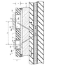
図1は、本発明の一実施形態に係る脈波センサー及びその周辺を示す一部断面図である。図1に示すように、脈波センサー1は、センサー基板10と、発光素子20と、反射光検出素子30とを含んでいる。センサー基板10は、互いに対向する第1の主面(図中上面)及び第2の主面(図中下面)を有し、第1及び第2の主面を貫通する第1の開口部10a及び第2の開口部10bが形成されている。センサー基板10としては、例えば、ガラスエポキシ基板を用いることができる。
FIG. 1 is a partial cross-sectional view showing a pulse wave sensor and its periphery according to an embodiment of the present invention. As shown in FIG. 1, the
発光素子20は、センサー基板10の第1の主面に実装され、第1の開口部10a内に挿入された発光面20aを有し、発光面20aから光を射出する。発光素子20としては、例えば、供給される駆動電流に応じた強度を有する光を射出するLED(発光ダイオード)を用いることができる。発光色としては、血液に吸収され易い波長を有する色(例えば、青色)が適している。発光素子20は、発光面20a上に配置されたレンズ部21をさらに有しても良い。レンズ部21を設けることにより、発光素子20の発光面20aから射出される光を収束させることができる。
The
反射光検出素子30は、センサー基板10の第1の主面に実装され、発光素子20の発光面20aから射出されてセンサー基板10の第2の主面側において反射された光が第2の開口部10bを通過して入射する検出面30aを有している。図1に示すように、反射光検出素子30の検出面30aは、センサー基板10側(図中下側)を向いている。反射光検出素子30は、検出面30aに入射する光を光電変換することにより、電気信号である脈波測定信号を生成する。反射光検出素子30としては、例えば、入射する光の強度に応じた検出電流を出力するPD(フォトダイオード)を用いることができる。
The reflected
センサー基板10の第2の主面に対向して、生体情報測定装置の一部である透明基板40が設けられている。透明基板40の材料としては、例えば、ガラス又はアクリルを用いることができる。センサー基板10及び透明基板40は、生体情報測定装置の筐体によって支持されている。生体情報測定装置が被験者の手首に装着された際に、透明基板40は、被験者の手首に向けられる。従って、発光素子20の発光面20aから射出された光は、被験者の手首に入射する。
A
被験者の手首に入射した光は、被験者の表皮を透過して、その奥にある真皮の中の血管に到達する。血管に到達した光の一部は、血管内を流れる血液によって吸収される。一方、血管に到達した光の内で血液によって吸収されなかった光の一部は、生体組織における散乱等を経た後に、反射光として反射光検出素子30の検出面30aに到達する。
The light incident on the subject's wrist passes through the subject's epidermis and reaches the blood vessel in the dermis behind it. Part of the light that reaches the blood vessel is absorbed by the blood flowing in the blood vessel. On the other hand, part of the light that has not been absorbed by the blood among the light that has reached the blood vessel reaches the
ここで、被験者の血管(特に、動脈)は、心拍と同じ周期で膨張と収縮とを繰り返している。従って、血管内を流れる血液による光の減衰量は、血管の膨張及び収縮の周期と同じ周期で時間的に変動する。そこで、被験者の血管を通過した光の強度を検出することにより、被験者の脈波を測定することができる。反射光検出素子30から出力される脈波測定信号は、測定部位における血管の容積変化を表す成分を有するものとなる。
Here, the blood vessels (particularly, arteries) of the subject repeat expansion and contraction in the same cycle as the heartbeat. Therefore, the attenuation amount of light by the blood flowing in the blood vessel fluctuates with time in the same cycle as the cycle of blood vessel expansion and contraction. Therefore, the pulse wave of the subject can be measured by detecting the intensity of light that has passed through the blood vessel of the subject. The pulse wave measurement signal output from the reflected
このような脈波センサー1の測定原理から分かるように、発光素子20から照射されて生体組織を介さずに反射光検出素子30に入射する光の強度が大きい場合には、脈波測定信号のSN比が低下して脈波測定を正確に行うことができない。従って、脈波測定の精度を向上させるためには、発光素子20から反射光検出素子30に直接的に入射する光を遮断する必要がある。
As can be seen from the measurement principle of the
そのために、本実施形態においては、センサー基板10が、少なくとも第1の開口部10aと第2の開口部10bとの間に非透明な部分を含んでいる。これにより、センサー基板10の非透明な部分が、発光素子20と反射光検出素子30との間を遮光する遮光壁として機能する。従って、発光素子20と反射光検出素子30との間を遮光するために特別な遮光部品をセンサー基板10に設ける必要がないので、脈波センサー1の厚さを薄くすると共に、脈波センサー1のコストダウンを図ることができる。
Therefore, in the present embodiment, the
ここで、センサー基板10が、発光素子20の発光面20aからセンサー基板10を介して反射光検出素子30の検出面30aに入射する光によって反射光検出素子30が反応しない程度の非透明性を有していることが望ましい。その場合には、発光素子20の発光面20aからセンサー基板10を介して反射光検出素子30の検出面30aに入射する光によって脈波測定信号のSN比が劣化するおそれがなくなる。
Here, the
センサー基板10が遮光壁として機能するためには、センサー基板10自体が、発光素子20から射出される光に対して低い透過率を有しても良い。あるいは、図1に示すように、センサー基板10が、第1の開口部10a又は第2の開口部10bの側面に形成された反射層又はメッキ層11を含んでも良い。反射層が、発光素子20から射出される光を反射し、又は、メッキ層が、発光素子20から射出される光を反射又は減衰させることにより、発光素子20の発光面20aからセンサー基板10を介して反射光検出素子30の検出面30aに入射する光を減少させることができる。
In order for the
一般的に、両面配線基板の場合には、スルーホールの壁面に無電解メッキにより銅(Cu)等の金属層を形成する方法が採用されている。従って、スルーホールを有する一般的な両面配線基板の製造工程を利用して、センサー基板10の第1の開口部10a又は第2の開口部10bの側面に、銅(Cu)又は銅合金等の金属の反射層又はメッキ層11を形成することができる。例えば、反射層又はメッキ層11の材料として、銅(Cu)を50%〜70%、ニッケル(Ni)を5%〜30%、亜鉛(Zn)を10%〜30%含む洋白を用いても良い。
Generally, in the case of a double-sided wiring board, a method of forming a metal layer such as copper (Cu) on the wall surface of the through hole by electroless plating is employed. Therefore, using a manufacturing process of a general double-sided wiring board having a through hole, copper (Cu) or a copper alloy or the like is formed on the side surface of the
図1において、発光素子20の中心軸と反射光検出素子30の中心軸との間の距離Dは、例えば、2mmであり、センサー基板10の厚さTは、例えば、0.65mmである。ここで、発光素子20の発光面20aが、センサー基板10の第2の主面よりも外側に突出しないことが望ましい。その場合には、発光素子20の発光面20aから射出される光の広がりが抑制されるので、生体組織以外の物体(透明基板40等)によって反射されて反射光検出素子30の検出面30aに入射する光の量を低減することができる。
In FIG. 1, the distance D between the central axis of the
ただし、発光素子20がレンズ部21を有する場合には、発光素子20の発光面20aから射出される光がレンズ部21によって収束されるので、レンズ部21は、センサー基板10の第2の主面よりも外側に突出しても良い。これにより、レンズ部21を設けるためにセンサー基板10を厚くする必要がなくなる。
However, when the
図2は、図1に示す脈波センサーの組立図である。図2に示すように、発光素子20は、複数の端子22を有している。また、反射光検出素子30も、複数の端子31を有している。発光素子20及び反射光検出素子30の複数の端子は、センサー基板の第1の主面に形成された複数の電極12及び13に、半田によってそれぞれ接続されても良い。
FIG. 2 is an assembly diagram of the pulse wave sensor shown in FIG. As shown in FIG. 2, the
その場合には、一般的な表面実装技術を用いることができる。即ち、クリーム半田印刷機を用いてセンサー基板10上への半田印刷を行った後に、チップマウンターを用いて発光素子20及び反射光検出素子30の実装を行い、発光素子20及び反射光検出素子30が実装されたセンサー基板10をリフロー炉に投入して半田を熔融させることにより、冷却後に発光素子20及び反射光検出素子30がセンサー基板10に固定される。
In that case, a general surface mounting technique can be used. That is, after performing solder printing on the
あるいは、反射光検出素子30は、図2に示すACF(Anisotropic Conductive Film:異方性導電フィルム)又はACP(Anisotropic Conductive Paste:異方性導電ペースト)14を用いて、センサー基板10の第1の主面にフリップチップボンディングによって実装されても良い。
Alternatively, the reflected
ACFは、微細な導電性粒子を熱硬化性樹脂に混ぜ合わせたものを膜状に成型して作製されたフィルムである。ここで、導電性粒子は、例えば、内側からニッケル層、金メッキ層、最も外側に絶縁層が重ねられた直径3μm〜5μm程度の球体である。また、ACPは、導電性粒子を樹脂内に拡散させて作製されたペーストであり、フィルムとして成型されていない点がACFと異なる。 ACF is a film produced by molding fine conductive particles mixed with a thermosetting resin into a film shape. Here, the conductive particles are, for example, spheres having a diameter of about 3 μm to 5 μm, in which a nickel layer, a gold plating layer, and an insulating layer are stacked on the outermost side. ACP is a paste produced by diffusing conductive particles in a resin, and is different from ACF in that it is not molded as a film.
反射光検出素子30の実装にACFを用いる場合には、反射光検出素子30の端子31とセンサー基板10の電極13との間にACFを挟み、ヒーター等で熱を加えながら弾力を有するゴム等のパッドで反射光検出素子30を加圧すると、端子31の凸部が当るフィルム部分のみに圧力がかかる。
When the ACF is used for mounting the reflected
その結果、フィルム内に分散している導電性粒子が接触しながら重なり、やがて押し付けられ、導電性粒子内のメッキ層同士が結合することによって縦方向(センサー基板10の第1の主面と略直交する方向)の導電経路が形成される。これにより、反射光検出素子30の端子31とセンサー基板10の電極13とが電気的に接続される。
As a result, the conductive particles dispersed in the film overlap with each other while being in contact with each other, and are eventually pressed to bond the plating layers in the conductive particles to each other in the longitudinal direction (substantially the first main surface of the sensor substrate 10). Conductive paths in the direction perpendicular to each other are formed. Thereby, the
一方、圧力がかからなかったフィルム部分における導電性粒子は、絶縁層を保持しているので、横方向(センサー基板10の第1の主面に略平行な方向)に並ぶ端子間の絶縁は保持される。即ち、縦方向には導電性を有し横方向には絶縁性を有する異方性が実現される。これにより、横方向に並ぶ端子間の間隔が狭くても、端子間の短絡を生じることなく反射光検出素子30を実装することができる。
On the other hand, since the conductive particles in the film portion where no pressure is applied hold the insulating layer, the insulation between the terminals arranged in the lateral direction (direction substantially parallel to the first main surface of the sensor substrate 10) is not caused. Retained. That is, anisotropy having conductivity in the vertical direction and insulation in the horizontal direction is realized. Thereby, even if the space | interval between the terminals arranged in a horizontal direction is narrow, the reflected
さらに、ACF又はACP14は、第2の開口部10bの周囲に亘って、反射光検出素子30とセンサー基板10の第1の主面との間に充填されても良い。あるいは、図2に示すように、NCF(Non-Conductive Film:非導電性フィルム)又はNCP(Non-Conductive Paste:非導電性ペースト)15が、第2の開口部10bの周囲に亘って、反射光検出素子30とセンサー基板10の第1の主面との間に充填されても良い。NCF又はNCPは、樹脂を主成分とし、電子部品を基板に接着するためのフィルム又はペーストである。
Furthermore, the ACF or
これにより、反射光検出素子30とセンサー基板10の第1の主面との間の隙間が塞がれるので、センサー基板10の第1の主面側から反射光検出素子30の検出面30aに漏れこむ光を遮断して、脈波測定信号のSN比を向上させることができる。また、これらのフィルム又はペーストは、流動性が小さいので、反射光検出素子30の検出面30aにまで流れ出すおそれがない。
As a result, the gap between the reflected
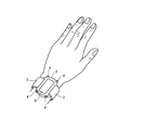
図3は、図1に示す脈波センサーを用いた生体情報測定装置の外観の一例を示す模式図である。この生体情報測定装置は、腕時計を模した形状を有しており、脈波測定機能に加えて、通常の腕時計としての計時機能を備えている。生体情報測定装置の筐体2には、バンド3が取り付けられており、バンド3を被験者の手首に巻きつけて締めることにより、生体情報測定装置が被験者の身体に装着される。
FIG. 3 is a schematic diagram showing an example of the appearance of a biological information measuring apparatus using the pulse wave sensor shown in FIG. This biological information measuring device has a shape imitating a wristwatch and has a timekeeping function as a normal wristwatch in addition to a pulse wave measurement function. A band 3 is attached to the
筐体2の外周部には、複数のボタンスイッチ4が設けられている。それらのボタンスイッチ4は、脈波の測定開始、測定終了、測定結果のリセット、及び、時刻設定等の各種の命令を入力するために用いられる。筐体2は、第1の面(表面)において、長方形状の表示面を有する表示部9を支持している。表示部9には、測定結果として脈拍間隔又は脈拍数が表示され、あるいは、通常の腕時計と同様に時刻が表示される。一方、筐体2は、第1の面に対向する第2の面(裏面)において、図1に示す透明基板40を支持している。ただし、図3に示す生体情報測定装置は、本実施形態に係る生体情報測定装置の一例に過ぎず、本実施形態に係る生体情報測定装置は、被験者の手首以外の部位に装着されるようにしても良い。
A plurality of button switches 4 are provided on the outer periphery of the
図4は、図1に示す脈波センサーを用いた生体情報測定装置の構成例を示すブロック図である。なお、図4においては、計時機能に関する構成は省略されている。図4に示すように、生体情報測定装置は、脈波センサー1と、アナログ回路5と、演算処理回路6と、データ格納部7と、音声出力部8と、表示部9とを含んでいる。ここで、脈波センサー1〜音声出力部8は、図3に示す筐体2に内蔵されている。また、アナログ回路5〜演算処理回路6は、脈波センサー1から出力される脈波測定信号に基づいて脈拍間隔又は脈拍数を測定する回路部を構成している。
FIG. 4 is a block diagram showing a configuration example of a biological information measuring apparatus using the pulse wave sensor shown in FIG. In FIG. 4, the configuration related to the timekeeping function is omitted. As shown in FIG. 4, the biological information measuring device includes a
アナログ回路5は、駆動回路51と、I/V変換回路52と、アンプ53とを含んでいる。駆動回路51は、脈波センサー1の発光素子20に駆動電流を供給することにより、発光素子20を発光させる。I/V変換回路52は、脈波センサー1の反射光検出素子30から出力される検出電流(脈波測定信号)を電圧に変換して、その電圧をアンプ53に出力する。アンプ53は、I/V変換回路52から出力される電圧を増幅して、増幅された電圧を演算処理回路6に出力する。
The
演算処理回路6は、A/D変換回路61と、CPU(中央演算装置)62と、RAM(ランダムアクセスメモリー)等の揮発性メモリー63と、ROM(リードオンリーメモリー)等の不揮発性メモリー64とを含んでいる。A/D変換回路61は、アンプ53から出力される電圧をアナログ/ディジタル変換することによって脈波測定データを生成し、脈波測定データをCPU62に出力する。
The
CPU62は、揮発性メモリー63をワークエリアとして利用しつつ、不揮発性メモリー64に記憶されている脈波解析プログラムに従って動作する。脈波解析プログラムは、脈波解析処理をCPU62に実行させる。脈波解析処理において、CPU62は、A/D変換回路61から出力される脈波測定データに基づいて脈拍間隔又は脈拍数を測定し、その測定結果をデータ格納部7に格納する。さらに、CPU62は、測定終了を知らせる音声を音声出力部8から出力させると共に、測定された脈拍間隔又は脈拍数を表示部9に表示させる。
The
次に、図3及び図4に示す生体情報測定装置の動作について説明する。被験者が、ボタンスイッチ4を用いて、脈波の測定開始の命令を入力すると、演算処理回路6のCPU62は、駆動回路51に発光素子20の発光を開始させる。これにより、発光素子20から射出された光が被験者の手首に入射する。
Next, the operation of the biological information measuring apparatus shown in FIGS. 3 and 4 will be described. When the subject inputs a pulse wave measurement start command using the button switch 4, the
被験者の手首に入射した光の一部は、血管を通過して反射され、反射光検出素子30に入射する。これにより、反射光検出素子30は、測定部位における血管の容積変化を表す成分を有する脈波測定信号を出力する。反射光検出素子30から出力される脈波測定信号は、アナログ回路5において処理され、演算処理回路6のA/D変換回路61によって脈波測定データに変換されて、CPU62に供給される。
Part of the light incident on the wrist of the subject is reflected through the blood vessel and enters the reflected
CPU62は、脈波測定データに基づいて脈拍間隔又は脈拍数を測定し、その測定結果をデータ格納部7に格納する。例えば、CPU62は、脈波測定データの値にピークが現れる度に、最新のピークと1つ前のピークとの間の時間差を求め、この時間差を脈拍間隔としてデータ格納部7に格納する。また、CPU62は、脈波測定データの値における所定時間(例えば、1分間)毎のピークの出現数をカウントし、カウントされた数を脈拍数としてデータ格納部7に格納する。さらに、CPU62は、データ格納部7に格納された脈拍間隔又は脈拍数を、測定結果として表示部9に表示させる。
The
上記の実施形態においては、腕時計型の生体情報測定装置に組み込まれた脈波センサーについて説明したが、本発明は、以上説明した実施形態に限定されるものではない。例えば、本発明は、被験者の手指や耳朶等を測定部位とする生体情報測定装置においても利用可能であり、当該技術分野において通常の知識を有する者によって、本発明の技術的思想内で多くの変形が可能である。 In the above embodiment, the pulse wave sensor incorporated in the wristwatch-type biological information measuring device has been described, but the present invention is not limited to the above-described embodiment. For example, the present invention can also be used in a biological information measuring device that uses a subject's finger or earlobe as a measurement site, and many people within the technical idea of the present invention have ordinary knowledge in the technical field. Deformation is possible.
1…脈波センサー、10…センサー基板、10a、10b…開口部、11…反射層又はメッキ層、12、13…電極、14…ACF又はACP、15…NCF又はNCP、20…発光素子、20a…発光面、21…レンズ部、22…端子、30…反射光検出素子、30a…検出面、31…端子、40…透明基板、2…筐体、3…バンド、4…ボタンスイッチ、5…アナログ回路、51…駆動回路、52…I/V変換回路、53…アンプ、6…演算処理回路、61…A/D変換回路、62…CPU、63…揮発性メモリー、64…不揮発性メモリー、7…データ格納部、8…音声出力部、9…表示部
DESCRIPTION OF
Claims (10)
前記第1の主面に実装され、前記第1の開口部内に挿入された発光面を有する発光素子と、
前記第1の主面に実装され、前記発光素子の発光面から射出されて前記第2の主面側において反射された光が前記第2の開口部を通過して入射する検出面を有する反射光検出素子と、
を具備する脈波センサー。 A first opening and a second opening that have a first main surface and a second main surface that face each other and penetrate the first and second main surfaces are formed, and at least the first opening is formed. A sensor substrate including a non-transparent portion between an opening and the second opening;
A light emitting device mounted on the first main surface and having a light emitting surface inserted into the first opening;
A reflection having a detection surface that is mounted on the first main surface and is incident on the light emitted from the light emitting surface of the light emitting element and reflected on the second main surface side through the second opening. A light detection element;
A pulse wave sensor comprising:
前記センサー基板の第2の主面に対向して設けられた透明基板と、
前記脈波センサーから出力される脈波測定信号に基づいて脈拍間隔又は脈拍数を測定する回路部と、
前記回路部の測定結果を表示する表示部と、
前記表示部を第1の面において支持すると共に前記透明基板を第1の面に対向する第2の面において支持し、前記脈波センサー及び前記回路部を内蔵する筐体と、
を具備する生体情報測定装置。 The pulse wave sensor according to any one of claims 1 to 9,
A transparent substrate provided facing the second main surface of the sensor substrate;
A circuit unit for measuring a pulse interval or a pulse rate based on a pulse wave measurement signal output from the pulse wave sensor;
A display unit for displaying a measurement result of the circuit unit;
A housing that supports the display unit on a first surface and supports the transparent substrate on a second surface opposite to the first surface, and includes the pulse wave sensor and the circuit unit;
A biological information measuring device comprising:
Priority Applications (3)
| Application Number | Priority Date | Filing Date | Title |
|---|---|---|---|
| JP2013219891A JP2015080601A (en) | 2013-10-23 | 2013-10-23 | Pulse wave sensor and biological information measuring device using the same |
| US14/515,750 US20150112207A1 (en) | 2013-10-23 | 2014-10-16 | Pulse wave sensor and biological information measuring device using the same |
| CN201410572915.XA CN104545867A (en) | 2013-10-23 | 2014-10-23 | Pulse wave sensor and biological information measuring device using the same |
Applications Claiming Priority (1)
| Application Number | Priority Date | Filing Date | Title |
|---|---|---|---|
| JP2013219891A JP2015080601A (en) | 2013-10-23 | 2013-10-23 | Pulse wave sensor and biological information measuring device using the same |
Publications (2)
| Publication Number | Publication Date |
|---|---|
| JP2015080601A true JP2015080601A (en) | 2015-04-27 |
| JP2015080601A5 JP2015080601A5 (en) | 2016-11-24 |
Family
ID=52826782
Family Applications (1)
| Application Number | Title | Priority Date | Filing Date |
|---|---|---|---|
| JP2013219891A Withdrawn JP2015080601A (en) | 2013-10-23 | 2013-10-23 | Pulse wave sensor and biological information measuring device using the same |
Country Status (3)
| Country | Link |
|---|---|
| US (1) | US20150112207A1 (en) |
| JP (1) | JP2015080601A (en) |
| CN (1) | CN104545867A (en) |
Cited By (4)
| Publication number | Priority date | Publication date | Assignee | Title |
|---|---|---|---|---|
| WO2020261981A1 (en) | 2019-06-24 | 2020-12-30 | 株式会社アイ・メデックス | Bioelectrode provided with electronic circuit board |
| JP2021534915A (en) * | 2018-09-04 | 2021-12-16 | アクティーア・ソシエテ・アノニム | A system that determines the blood pressure of one or more users |
| JP2022532603A (en) * | 2019-05-14 | 2022-07-15 | 華為技術有限公司 | Smart wearable device |
| WO2023145226A1 (en) * | 2022-01-31 | 2023-08-03 | 太陽誘電株式会社 | Pulse wave detection device |
Families Citing this family (8)
| Publication number | Priority date | Publication date | Assignee | Title |
|---|---|---|---|---|
| KR102414780B1 (en) * | 2015-06-10 | 2022-06-29 | 삼성디스플레이 주식회사 | Display apparatus |
| EP3162285B1 (en) * | 2015-10-27 | 2021-12-08 | Nokia Technologies Oy | A sensor element |
| US9943239B2 (en) * | 2016-03-07 | 2018-04-17 | Taiwan Semiconductor Manufacturing Company Ltd. | Optical sensing system and associated electronic device |
| JP6750294B2 (en) * | 2016-04-28 | 2020-09-02 | オムロンヘルスケア株式会社 | Pulse wave detection device and biological information measurement device |
| TWI605791B (en) * | 2016-11-10 | 2017-11-21 | Light-sensing device for wearable devices | |
| US10918322B2 (en) * | 2017-02-13 | 2021-02-16 | Apple Inc. | Light restriction designs in optical sensing applications having shared windows |
| JP7134246B2 (en) * | 2018-10-30 | 2022-09-09 | 京セラ株式会社 | Optical sensor device |
| CN109461751B (en) * | 2018-11-14 | 2021-10-12 | 京东方科技集团股份有限公司 | Photoelectric detection device, preparation method thereof, heart rate detection device and electronic equipment |
Citations (7)
| Publication number | Priority date | Publication date | Assignee | Title |
|---|---|---|---|---|
| US3769974A (en) * | 1971-06-29 | 1973-11-06 | Martin Marietta Corp | Blood pulse measuring employing reflected red light |
| JPH10509352A (en) * | 1994-11-01 | 1998-09-14 | マシモ コーポレイション | Low noise optical probe |
| JP2005040261A (en) * | 2003-07-25 | 2005-02-17 | Waatekkusu:Kk | Pulse wave sensor |
| WO2006051726A1 (en) * | 2004-11-09 | 2006-05-18 | Kyushu University, National University Corporation | Sensor part and biological sensor |
| JP2006234851A (en) * | 2005-02-21 | 2006-09-07 | Bridgestone Corp | Optical device and its manufacturing method |
| JP2011251007A (en) * | 2010-06-02 | 2011-12-15 | Alps Electric Co Ltd | Bio-pulse wave sensor and bio-pulse wave measuring device |
| JP2013009709A (en) * | 2011-06-28 | 2013-01-17 | Seiko Epson Corp | Biosensor and biological information detector |
Family Cites Families (4)
| Publication number | Priority date | Publication date | Assignee | Title |
|---|---|---|---|---|
| JP3882756B2 (en) * | 2003-01-30 | 2007-02-21 | 日本電信電話株式会社 | Blood flow sensor and blood flow meter |
| JP2009150690A (en) * | 2007-12-19 | 2009-07-09 | Nichicon Corp | Reflection-type optical sensor |
| US8779349B2 (en) * | 2011-03-08 | 2014-07-15 | Fluke Corporation | Minimizing ambient light in a feedback circuit in pulse oximeter test instruments |
| US8954135B2 (en) * | 2012-06-22 | 2015-02-10 | Fitbit, Inc. | Portable biometric monitoring devices and methods of operating same |
-
2013
- 2013-10-23 JP JP2013219891A patent/JP2015080601A/en not_active Withdrawn
-
2014
- 2014-10-16 US US14/515,750 patent/US20150112207A1/en not_active Abandoned
- 2014-10-23 CN CN201410572915.XA patent/CN104545867A/en active Pending
Patent Citations (7)
| Publication number | Priority date | Publication date | Assignee | Title |
|---|---|---|---|---|
| US3769974A (en) * | 1971-06-29 | 1973-11-06 | Martin Marietta Corp | Blood pulse measuring employing reflected red light |
| JPH10509352A (en) * | 1994-11-01 | 1998-09-14 | マシモ コーポレイション | Low noise optical probe |
| JP2005040261A (en) * | 2003-07-25 | 2005-02-17 | Waatekkusu:Kk | Pulse wave sensor |
| WO2006051726A1 (en) * | 2004-11-09 | 2006-05-18 | Kyushu University, National University Corporation | Sensor part and biological sensor |
| JP2006234851A (en) * | 2005-02-21 | 2006-09-07 | Bridgestone Corp | Optical device and its manufacturing method |
| JP2011251007A (en) * | 2010-06-02 | 2011-12-15 | Alps Electric Co Ltd | Bio-pulse wave sensor and bio-pulse wave measuring device |
| JP2013009709A (en) * | 2011-06-28 | 2013-01-17 | Seiko Epson Corp | Biosensor and biological information detector |
Cited By (5)
| Publication number | Priority date | Publication date | Assignee | Title |
|---|---|---|---|---|
| JP2021534915A (en) * | 2018-09-04 | 2021-12-16 | アクティーア・ソシエテ・アノニム | A system that determines the blood pressure of one or more users |
| JP7361763B2 (en) | 2018-09-04 | 2023-10-16 | アクティーア・ソシエテ・アノニム | System for determining blood pressure of one or more users |
| JP2022532603A (en) * | 2019-05-14 | 2022-07-15 | 華為技術有限公司 | Smart wearable device |
| WO2020261981A1 (en) | 2019-06-24 | 2020-12-30 | 株式会社アイ・メデックス | Bioelectrode provided with electronic circuit board |
| WO2023145226A1 (en) * | 2022-01-31 | 2023-08-03 | 太陽誘電株式会社 | Pulse wave detection device |
Also Published As
| Publication number | Publication date |
|---|---|
| CN104545867A (en) | 2015-04-29 |
| US20150112207A1 (en) | 2015-04-23 |
Similar Documents
| Publication | Publication Date | Title |
|---|---|---|
| JP2015080601A (en) | Pulse wave sensor and biological information measuring device using the same | |
| JP5742104B2 (en) | Optical device and biological information detector | |
| US11246498B2 (en) | Sensor, sensor device, and sensor system | |
| CN103747723A (en) | Living organism sensor | |
| JP5446915B2 (en) | Biological information detector and biological information measuring device | |
| JP2013009710A (en) | Biosensor and biological information detection device | |
| CN209804634U (en) | Optical device package | |
| US20230246012A1 (en) | Optical sensor package structure and electronic device | |
| JP2013000158A (en) | Biosensor and biological information detection apparatus | |
| JP2010200970A (en) | Optical sensor and method for manufacturing the same | |
| JP5772292B2 (en) | Biological sensor and biological information detection apparatus | |
| JP2019192702A (en) | Semiconductor device and sensor modular | |
| CN216250727U (en) | Chip packaging structure and electronic equipment | |
| JP2016000205A (en) | Biological body sensor and biological body information detector | |
| WO2021053962A1 (en) | Semiconductor laser drive device, electronic apparatus, and method for manufacturing semiconductor laser drive device | |
| JP7411350B2 (en) | Distance measuring device, electronic equipment, and method for manufacturing a ranging device | |
| KR20170133022A (en) | Wearable device and method for manufacturing method thereof | |
| JP6323088B2 (en) | Photodetection unit and biological information detection apparatus | |
| US11033193B2 (en) | Light emitting device, biological information measuring apparatus, and method of manufacturing light emitting device | |
| KR20170019882A (en) | Sensor and detection apparatus including the same | |
| JP2016096977A (en) | Optical sensor module | |
| KR102422136B1 (en) | Wearable device and method for manufacturing method thereof | |
| JP7395848B2 (en) | Biological information measuring device | |
| JP2011161039A (en) | Biological information detector and biological information measuring device | |
| WO2020026617A1 (en) | Blood flow sensor and information processing device |
Legal Events
| Date | Code | Title | Description |
|---|---|---|---|
| RD04 | Notification of resignation of power of attorney |
Free format text: JAPANESE INTERMEDIATE CODE: A7424 Effective date: 20160617 |
|
| RD03 | Notification of appointment of power of attorney |
Free format text: JAPANESE INTERMEDIATE CODE: A7423 Effective date: 20160627 |
|
| A521 | Request for written amendment filed |
Free format text: JAPANESE INTERMEDIATE CODE: A523 Effective date: 20161011 |
|
| A621 | Written request for application examination |
Free format text: JAPANESE INTERMEDIATE CODE: A621 Effective date: 20161011 |
|
| A977 | Report on retrieval |
Free format text: JAPANESE INTERMEDIATE CODE: A971007 Effective date: 20170530 |
|
| A131 | Notification of reasons for refusal |
Free format text: JAPANESE INTERMEDIATE CODE: A131 Effective date: 20170704 |
|
| A761 | Written withdrawal of application |
Free format text: JAPANESE INTERMEDIATE CODE: A761 Effective date: 20170831 |