JP2015040987A - Organic el display device - Google Patents
Organic el display device Download PDFInfo
- Publication number
- JP2015040987A JP2015040987A JP2013172094A JP2013172094A JP2015040987A JP 2015040987 A JP2015040987 A JP 2015040987A JP 2013172094 A JP2013172094 A JP 2013172094A JP 2013172094 A JP2013172094 A JP 2013172094A JP 2015040987 A JP2015040987 A JP 2015040987A
- Authority
- JP
- Japan
- Prior art keywords
- organic
- display
- power consumption
- low power
- image data
- Prior art date
- Legal status (The legal status is an assumption and is not a legal conclusion. Google has not performed a legal analysis and makes no representation as to the accuracy of the status listed.)
- Pending
Links
Images


Classifications
-
- G—PHYSICS
- G09—EDUCATION; CRYPTOGRAPHY; DISPLAY; ADVERTISING; SEALS
- G09G—ARRANGEMENTS OR CIRCUITS FOR CONTROL OF INDICATING DEVICES USING STATIC MEANS TO PRESENT VARIABLE INFORMATION
- G09G5/00—Control arrangements or circuits for visual indicators common to cathode-ray tube indicators and other visual indicators
- G09G5/36—Control arrangements or circuits for visual indicators common to cathode-ray tube indicators and other visual indicators characterised by the display of a graphic pattern, e.g. using an all-points-addressable [APA] memory
- G09G5/39—Control of the bit-mapped memory
- G09G5/395—Arrangements specially adapted for transferring the contents of the bit-mapped memory to the screen
-
- G—PHYSICS
- G09—EDUCATION; CRYPTOGRAPHY; DISPLAY; ADVERTISING; SEALS
- G09G—ARRANGEMENTS OR CIRCUITS FOR CONTROL OF INDICATING DEVICES USING STATIC MEANS TO PRESENT VARIABLE INFORMATION
- G09G3/00—Control arrangements or circuits, of interest only in connection with visual indicators other than cathode-ray tubes
- G09G3/20—Control arrangements or circuits, of interest only in connection with visual indicators other than cathode-ray tubes for presentation of an assembly of a number of characters, e.g. a page, by composing the assembly by combination of individual elements arranged in a matrix no fixed position being assigned to or needed to be assigned to the individual characters or partial characters
- G09G3/22—Control arrangements or circuits, of interest only in connection with visual indicators other than cathode-ray tubes for presentation of an assembly of a number of characters, e.g. a page, by composing the assembly by combination of individual elements arranged in a matrix no fixed position being assigned to or needed to be assigned to the individual characters or partial characters using controlled light sources
- G09G3/30—Control arrangements or circuits, of interest only in connection with visual indicators other than cathode-ray tubes for presentation of an assembly of a number of characters, e.g. a page, by composing the assembly by combination of individual elements arranged in a matrix no fixed position being assigned to or needed to be assigned to the individual characters or partial characters using controlled light sources using electroluminescent panels
- G09G3/32—Control arrangements or circuits, of interest only in connection with visual indicators other than cathode-ray tubes for presentation of an assembly of a number of characters, e.g. a page, by composing the assembly by combination of individual elements arranged in a matrix no fixed position being assigned to or needed to be assigned to the individual characters or partial characters using controlled light sources using electroluminescent panels semiconductive, e.g. using light-emitting diodes [LED]
- G09G3/3208—Control arrangements or circuits, of interest only in connection with visual indicators other than cathode-ray tubes for presentation of an assembly of a number of characters, e.g. a page, by composing the assembly by combination of individual elements arranged in a matrix no fixed position being assigned to or needed to be assigned to the individual characters or partial characters using controlled light sources using electroluminescent panels semiconductive, e.g. using light-emitting diodes [LED] organic, e.g. using organic light-emitting diodes [OLED]
-
- G—PHYSICS
- G09—EDUCATION; CRYPTOGRAPHY; DISPLAY; ADVERTISING; SEALS
- G09G—ARRANGEMENTS OR CIRCUITS FOR CONTROL OF INDICATING DEVICES USING STATIC MEANS TO PRESENT VARIABLE INFORMATION
- G09G2310/00—Command of the display device
- G09G2310/04—Partial updating of the display screen
-
- G—PHYSICS
- G09—EDUCATION; CRYPTOGRAPHY; DISPLAY; ADVERTISING; SEALS
- G09G—ARRANGEMENTS OR CIRCUITS FOR CONTROL OF INDICATING DEVICES USING STATIC MEANS TO PRESENT VARIABLE INFORMATION
- G09G2320/00—Control of display operating conditions
- G09G2320/04—Maintaining the quality of display appearance
- G09G2320/043—Preventing or counteracting the effects of ageing
- G09G2320/046—Dealing with screen burn-in prevention or compensation of the effects thereof
-
- G—PHYSICS
- G09—EDUCATION; CRYPTOGRAPHY; DISPLAY; ADVERTISING; SEALS
- G09G—ARRANGEMENTS OR CIRCUITS FOR CONTROL OF INDICATING DEVICES USING STATIC MEANS TO PRESENT VARIABLE INFORMATION
- G09G2330/00—Aspects of power supply; Aspects of display protection and defect management
- G09G2330/02—Details of power systems and of start or stop of display operation
- G09G2330/021—Power management, e.g. power saving
Landscapes
- Engineering & Computer Science (AREA)
- Physics & Mathematics (AREA)
- General Physics & Mathematics (AREA)
- Theoretical Computer Science (AREA)
- Computer Hardware Design (AREA)
- Control Of Indicators Other Than Cathode Ray Tubes (AREA)
- Control Of El Displays (AREA)
- Electroluminescent Light Sources (AREA)
Abstract
Description
本発明は、有機EL表示装置に係わり、特に、低消費電力駆動時に有効な技術に関する。 The present invention relates to an organic EL display device, and more particularly to a technique effective at the time of driving with low power consumption.
近年、フラットディスプレイ装置の需要が増大している。特に、有機EL(Electro Luminescence)素子(OLED;Oganic Light Emitting Diode)を用いた有機EL表示装置は、消費電力、軽さ、薄さ、動画特性、視野角などの点で優れており、開発、実用化も進んでいる。
スマートフォンなどに用いられる有機EL表示装置の有機表示パネルは高精細化が進んでいるが、これに伴い消費電力の増加が問題となっている。
しかし、スマートフォンであっても、使用するさまざまな状況下では常に高精細の表示が必要とされているわけではなく、時間と日付、機器の状態表示(電波強度、バッテリ残量)、通信情報(着信来歴、メール着信)などの基本的な情報の表示だけでよい場合もある。
しかしながら、有機EL表示装置では、従来の携帯電話のようなサブ画面が搭載されていないため、有機EL表示パネルを使用するスマートフォンでは、少量の情報表示においても大画面の有機EL表示パネルを動作させる必要があり、消費電力の増大につながっていた。
In recent years, the demand for flat display devices has increased. In particular, an organic EL display device using an organic EL (Electro Luminescence) element (OLED: Organic Light Emitting Diode) is excellent in terms of power consumption, lightness, thinness, moving image characteristics, viewing angle, etc. Practical use is also progressing.
An organic display panel of an organic EL display device used for a smart phone or the like has been improved in definition, but with this, an increase in power consumption has become a problem.
However, even for smartphones, high-definition display is not always required under various circumstances, such as time and date, device status display (signal strength, battery level), communication information ( In some cases, it is only necessary to display basic information such as incoming call history, incoming mail).
However, since the organic EL display device is not equipped with a sub-screen like a conventional mobile phone, a smartphone using the organic EL display panel operates the large-screen organic EL display panel even when displaying a small amount of information. It was necessary and led to an increase in power consumption.
携帯電話向け液晶表示装置では、部分的に駆動して消費電力を低減させるパーシャル駆動が提案されていたが、液晶表示装置では光源となる照明装置の消費電力が圧倒的に大きく電力低減効果は少なかった。
このパーシャル駆動を、有機EL表示パネルなどのように、表示階調と表示画素数で消費電力が増加する表示装置に適用すると、消費電力の低減効果は大きい。
しかしながら、有機EL表示パネルにおいて、パーシャル駆動で部分表示を行うと、常時表示される有機EL素子が劣化し、焼付きが発生する。これを回避するために、部分表示の表示位置を変更するために、ホスト側から通常動作と同様に映像を入力すると、ホスト側の消費電力が増加するという問題点があった。
なお、前述の特許文献1には、「電源の起動時に予め記憶された以前の表示位置と異なる位置に表示を行い焼付きを防止する方法」が提案されているが、電源起動の周期は制御できないため焼付き防止の効果は限定的であった。
本発明は、前記従来技術の問題点を解決するためになされたものであり、本発明の目的は、表示したい画像データ量が少ない低消費電力駆動の場合に、焼付きの発生を防止することが可能となる技術を提供することにある。
本発明の前記ならびにその他の目的と新規な特徴は、本明細書の記述及び添付図面によって明らかにする。
In liquid crystal display devices for mobile phones, partial driving has been proposed to reduce the power consumption by partially driving, but in the liquid crystal display device, the power consumption of the lighting device as the light source is overwhelmingly large and the power reduction effect is small. It was.
When this partial drive is applied to a display device such as an organic EL display panel in which power consumption increases with display gradation and the number of display pixels, the effect of reducing power consumption is great.
However, in the organic EL display panel, when partial display is performed by partial driving, the organic EL element that is always displayed deteriorates and burn-in occurs. In order to avoid this, if a video is input from the host side in the same way as the normal operation in order to change the display position of the partial display, there is a problem that the power consumption on the host side increases.
In addition, the above-mentioned Patent Document 1 proposes a “method for displaying images at a position different from the previous display position stored in advance when the power supply is activated to prevent burn-in”, but the power activation cycle is controlled. Since it was not possible, the effect of preventing seizure was limited.
The present invention has been made to solve the problems of the prior art, and an object of the present invention is to prevent the occurrence of burn-in in the case of low power consumption driving with a small amount of image data to be displayed. It is to provide a technology that makes it possible.
The above and other objects and novel features of the present invention will become apparent from the description of this specification and the accompanying drawings.
本願において開示される発明のうち、代表的なものの概要を簡単に説明すれば、下記の通りである。
(1)通常駆動時と、低消費電力駆動時とを有し、前記低消費電力駆動時に、有機EL表示パネルに固定表示パターンを表示する有機EL表示装置であって、前記低消費電力駆動時に、前記有機EL表示パネルに表示する前記固定表示パターンの表示位置を、各フレーム毎に変更させる手段を有する。
(2)通常駆動時と、低消費電力駆動時とを有し、前記低消費電力駆動時に、有機EL表示パネルに固定表示パターンを表示する有機EL表示装置であって、前記有機EL表示パネルは、各画素に映像電圧を入力する映像線を有し、駆動回路を有し、前記駆動回路は、前記低消費電力駆動時に、制御信号を生成する内部制御信号生成回路と、前記低消費電力駆動時に、前記有機EL表示パネルに表示する前記固定表示パターンの画像データを格納するメモリと、前記メモリから読み出した画像データを映像電圧に変換し、前記映像線に供給する映像電圧出力手段と、前記メモリから読み出す前記画像データの読み出しタイミングを変更する手段とを有し、前記低消費電力駆動時に、前記メモリから読み出す前記画像データの読み出しタイミングを変更し、前記有機EL表示パネルに表示する前記固定表示パターンの表示位置を、各フレーム毎に変更させる。
(3)(1)または(2)において、前記固定表示パターンの表示位置は、前記各フレーム毎に所定の順番で、あるいは、前記各フレーム毎にランダムに変更される。
Of the inventions disclosed in this application, the outline of typical ones will be briefly described as follows.
(1) An organic EL display device that has a normal driving time and a low power consumption driving time and displays a fixed display pattern on the organic EL display panel during the low power consumption driving time. And means for changing the display position of the fixed display pattern displayed on the organic EL display panel for each frame.
(2) An organic EL display device that has a normal driving time and a low power consumption driving time and displays a fixed display pattern on the organic EL display panel at the time of the low power consumption driving. A video line for inputting a video voltage to each pixel, and a drive circuit, wherein the drive circuit generates an internal control signal when the low power consumption drive, and the low power consumption drive A memory for storing the image data of the fixed display pattern to be displayed on the organic EL display panel; a video voltage output means for converting the image data read from the memory into a video voltage and supplying the video voltage; Means for changing the read timing of the image data read from the memory, and the read timing of the image data read from the memory during the low power consumption driving Change the, the display position of the fixed display pattern to be displayed on the organic EL display panel, and changes for each frame.
(3) In (1) or (2), the display position of the fixed display pattern is changed in a predetermined order for each frame or randomly for each frame.
本願において開示される発明のうち代表的なものによって得られる効果を簡単に説明すれば、下記の通りである。
本発明の有機EL表示装置によれば、表示したい画像データ量が少ない低消費電力駆動の場合に、焼付きの発生を防止することが可能となる。
The effects obtained by the representative ones of the inventions disclosed in the present application will be briefly described as follows.
According to the organic EL display device of the present invention, it is possible to prevent image sticking in the case of low power consumption driving with a small amount of image data to be displayed.
以下、図面を参照して本発明の実施例を詳細に説明する。
なお、実施例を説明するための全図において、同一機能を有するものは同一符号を付け、その繰り返しの説明は省略する。また、以下の実施例は、本発明の特許請求の範囲の解釈を限定するためのものではない。
[実施例]
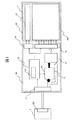
図1は、本発明の実施例の有機EL表示装置の概略内部構成を示すブロック図である。
図1において、1は有機EL表示装置であり、本実施例の有機EL表示装置1は、スマートフォン、タブレットなどに使用される小型の有機EL表示装置である。
本実施例の有機EL表示パネルは、例えば、トップエミッション方式で、かつ、白色発光層を用い、R,G,Bのカラーフィルタ層を通すことで、カラー画像を得るカラーフィルタ方式の有機EL表示パネルである。
2は、スマートフォン、タブレットのメイン制御回路に内蔵、または、付属された画像処理回路であり、画像処理回路2は、画像出力回路221を有する。
有機EL表示装置1は、有機EL駆動回路10、有機EL表示パネル20を有する。有機EL表示パネル20は、映像線(図示せず)と走査線(図示せず)とを有し、その内部に走査線(ゲートともいう)駆動回路21が設けられている。
有機EL駆動回路10は、外部の画像処理回路2の画像出力回路221からの画像データ、制御信号が入力されるインターフェース回路11と、駆動信号を出力する表示制御回路12と、走査線制御回路13と、外部から入力される画像データが格納されるフレームメモリ14と、画像制御回路15と、映像信号出力回路16とを有する。表示制御回路12は、内部制御信号生成回路121を有する。
Hereinafter, embodiments of the present invention will be described in detail with reference to the drawings.
In all the drawings for explaining the embodiments, parts having the same functions are given the same reference numerals, and repeated explanation thereof is omitted. Also, the following examples are not intended to limit the interpretation of the scope of the claims of the present invention.
[Example]
FIG. 1 is a block diagram showing a schematic internal configuration of an organic EL display device according to an embodiment of the present invention.
In FIG. 1, reference numeral 1 denotes an organic EL display device, and the organic EL display device 1 of this embodiment is a small organic EL display device used for a smartphone, a tablet, or the like.
The organic EL display panel of the present embodiment is, for example, a top emission method, a white light emitting layer, and a color filter type organic EL display that obtains a color image by passing the R, G, B color filter layers. It is a panel.
Reference numeral 2 denotes an image processing circuit built in or attached to a main control circuit of a smartphone or tablet. The image processing circuit 2 includes an
The organic EL display device 1 includes an organic
The organic
通常の駆動時では、外部の画像処理回路2の画像出力回路221から出力され、インターフェース回路11を介して入力された制御信号は、表示制御回路12に入力され、表示制御回路12は、当該制御信号に基づき、駆動信号を生成し、走査線制御回路13と、映像信号出力回路16に駆動信号を送出する。
走査線制御回路13は、表示制御回路12から入力される駆動信号に基づき、走査線駆動回路21を制御し、走査線駆動回路21は、走査線制御回路13から入力される走査線スキャン開始信号に基づき、1フレーム期間内に、有機EL表示パネル20内の走査線に、各画素に映像電圧を書き込むための選択電圧を順次供給する。
外部の画像処理回路2の画像出力回路221から出力された映像データは、γ補正等の処理を行う画像制御回路15に入力される。
画像制御回路15は、画像データを映像信号出力回路16に出力する。映像信号出力回路16は、画像データを、アナログの映像電圧に変換した後、表示制御回路12から入力される映像電圧出力タイミング信号に基づき、当該アナログの映像電圧を、有機EL表示パネル20内の映像線に出力する。
これにより、有機EL表示パネル20の表示領域ARに画像が表示される。
During normal driving, a control signal output from the
The scanning
Video data output from the
The
As a result, an image is displayed in the display area AR of the organic
一方、通常駆動に対して、低消費電力駆動の場合は、時間と日付、機器の状態表示(電波強度、バッテリ残量)、通信情報(着信来歴、メール着信)など基本的な情報の表示(以下、固定表示パターン)だけでよい場合もある。
このような場合に、外部の画像処理回路2の画像出力回路221から出力され、インターフェース回路11を介して入力された制御信号(タイミング信号や制御コマンド)に代えて、表示制御回路12は、内部制御信号生成回路121で生成される制御信号により、走査線制御回路13と、映像信号出力回路16を駆動するための駆動信号を生成するとともに、フレームメモリ14から画像データを読み出すための読出しタイミング信号を生成する。
低消費電力駆動の場合は、固定表示パターンを表示するためのR(赤),G(緑),B(青)の画像データは、フレームメモリ14に格納され、書き換えが行われるまで、表示制御回路12の内部制御信号生成回路121で生成された読出しタイミング信号により読み出され、γ補正等の処理を行う画像制御回路15に入力され、画像制御回路15は、画像データを映像信号出力回路16に出力する。
ここで、フレームメモリ14は、低消費電力駆動時に、有機EL表示パネル20に固定表示パターンを表示(即ち、部分表示)することが目的であるため、有機EL表示パネル20の精細度及び表示階調に対して小さくてもよい。
さらに、フレームメモリ14を内蔵することで、通常の動作時は、画像処理回路2の画像出力回路221からは、表示領域(AR)の全画素の画像データをリフレッシュ周波数の頻度で出力しているが、本実施例では、この出力に必要となる消費電力を必要最低限まで減少させることができる。
On the other hand, in the case of low power consumption driving compared to normal driving, basic information display such as time and date, device status display (signal strength, remaining battery level), communication information (call history, incoming mail) Hereinafter, only a fixed display pattern) may be required.
In such a case, instead of the control signal (timing signal or control command) output from the
In the case of low power consumption driving, R (red), G (green), and B (blue) image data for displaying a fixed display pattern is stored in the
Here, since the
Further, by incorporating the
図2は、本発明の実施例の有機EL表示装置における、低消費電力駆動時の走査線スキャン開始信号に対するフレームメモリの読出しタイミングを説明するためのタイミングチャートである。
図2において、Aは、低消費電力駆動時の各フレームの走査線スキャン開始信号、Bは、フレームメモリ14の読出しタイミング、C1〜C4は、読み出し画像データを示す。
前述したように、低消費電力駆動の場合は、時間と日付、機器の状態表示(電波強度、バッテリ残量)、通信情報(着信来歴、メール着信)などの基本的な情報の表示(固定表示パターン)だけでよいが、このような固定表示パターンを、同一の表示位置に表示すると、当該部分の有機EL素子が劣化し、焼付き現象が発生する。
そこで、本実施例では、図2に示すように、低消費電力駆動時に、各フレームの走査線スキャン開始信号Aに同期して、フレームメモリ14から画像データを読み出すタイミングを、所定の周期、例えば、図2のC1〜C4のように変更する。
これにより、固定表示パターン(時間と日付、機器の状態表示(電波強度、バッテリ残量)、通信情報(着信来歴、メール着信)など基本的な情報の表示)の表示位置が変更され、当該部分の有機EL素子が劣化し、焼付き現象の発生を抑制することができる。
FIG. 2 is a timing chart for explaining the reading timing of the frame memory with respect to the scanning line scan start signal at the time of low power consumption driving in the organic EL display device of the embodiment of the present invention.
In FIG. 2, A indicates a scanning line scan start signal for each frame during low power consumption driving, B indicates a read timing of the
As described above, in the case of low power consumption drive, basic information display (fixed display) such as time and date, device status display (signal strength, remaining battery level), communication information (call history, incoming mail), etc. However, if such a fixed display pattern is displayed at the same display position, the organic EL element in the portion deteriorates and a burn-in phenomenon occurs.
Therefore, in this embodiment, as shown in FIG. 2, the timing for reading image data from the
This changes the display position of the fixed display pattern (time and date, device status display (signal strength, remaining battery level), communication information (basic information such as incoming call history, incoming mail)), and so on. The organic EL element is deteriorated, and the occurrence of a seizure phenomenon can be suppressed.
図3、図4は、本発明の実施例の有機EL表示装置における、低消費電力駆動時の固定表示パターンの表示位置を説明するための概略図である。
図3、図4において、100は、低消費電力駆動時に、有機EL表示パネル20の表示領域ARに表示される固定表示パターンである。
図3に示す例では、低消費電力駆動時に、この固定表示パターン100の表示位置が、各フレーム毎に、3C1→3C2→3C3→3C4の順に移動し、その後、始めに戻って、各フレーム毎に、3C1→3C2→3C3→3C4の順に移動し、以後同じことを繰り返す。
図4に示す例では、低消費電力駆動時に、この固定表示パターン100の表示位置が、各フレーム毎に、3C1→3C2→3C3→3C4→3C5→3C6の順に移動し、その後、始めに戻って、各フレーム毎に、3C1→3C2→3C3→3C4→3C5→3C6の順に移動し、以後同じことを繰り返す。
なお、固定表示パターン100の表示位置は、図3、図4に示すように、規則的変化させる代わりに、領域101内において、固定表示パターン100の表示位置をランダムに変化させるようにしてもよい。
3 and 4 are schematic diagrams for explaining the display position of the fixed display pattern during low power consumption driving in the organic EL display device according to the embodiment of the present invention.
3 and 4,
In the example shown in FIG. 3, the display position of the fixed
In the example shown in FIG. 4, the display position of the fixed
As shown in FIGS. 3 and 4, the display position of the fixed
以上説明したように、本実施例では、低消費電力駆動時に、時間と日付、機器の状態表示(電波強度、バッテリ残量)、通信情報(着信来歴、メール着信)など基本的な情報(固定表示パターン)の表示位置が変更され、当該部分の有機EL素子が劣化し、焼付き現象の発生を抑制することができる。
なお、基本的な情報の移動量は、有機EL表示パネルの画素数に対するフレームメモリ14の容量の割合以上に動かすことで、移動前後で固定表示パターンは重ならないが、数画素程度の移動でも、固定表示パターンの表示による焼付き現象の抑制には効果がある。
また、本実施例の低消費電力駆動時には、階調の削減、表示のリフレッシュ周波数の低減、などの低消費電力となる組み合わせることでさらなる低消費電力化を実現できる。
このように、本発明の有機EL表示装置によれば、表示したい画像データ量が少ない低消費電力駆動の場合に、焼付きを発生することなく、有機EL表示装置に供給する電力と映像送信の為の電力をそれぞれ低減することが可能となる。
以上、本発明者によってなされた発明を、前記実施例に基づき具体的に説明したが、本発明は、前記実施例に限定されるものではなく、その要旨を逸脱しない範囲において種々変更可能であることは勿論である。
As described above, in this embodiment, basic information (fixed) such as time and date, device status display (signal strength, remaining battery level), communication information (call history, incoming mail), etc., when driving with low power consumption. The display position of the display pattern) is changed, the organic EL element in the portion is deteriorated, and the occurrence of the image sticking phenomenon can be suppressed.
In addition, the movement amount of the basic information is moved to a ratio of the capacity of the
Further, at the time of low power consumption driving of this embodiment, further reduction in power consumption can be realized by combining low power consumption such as gradation reduction and display refresh frequency.
As described above, according to the organic EL display device of the present invention, in the case of low power consumption driving with a small amount of image data to be displayed, the electric power supplied to the organic EL display device and video transmission can be performed without causing burn-in. Therefore, it becomes possible to reduce the electric power for each.
As mentioned above, the invention made by the present inventor has been specifically described based on the above embodiments. However, the present invention is not limited to the above embodiments, and various modifications can be made without departing from the scope of the invention. Of course.
1 有機EL表示装置
2 画像処理回路
10 有機EL駆動回路
11 インターフェース回路
12 表示制御回路
13 走査線制御回路
14 フレームメモリ
15 画像制御回路
16 映像信号出力回路
20 有機EL表示パネル
21 走査線駆動回路
100 固定表示パターン
101 領域
121 内部制御信号生成回路
221 画像出力回路
AR 表示領域
DESCRIPTION OF SYMBOLS 1 Organic EL display device 2
Claims (4)
前記低消費電力駆動時に、有機EL表示パネルに固定表示パターンを表示する有機EL表示装置であって、
前記低消費電力駆動時に、前記有機EL表示パネルに表示する前記固定表示パターンの表示位置を、各フレーム毎に変更させる手段を有することを特徴とする有機EL表示装置。 It has normal driving time and low power consumption driving time,
An organic EL display device that displays a fixed display pattern on an organic EL display panel during the low power consumption driving,
An organic EL display device comprising: means for changing a display position of the fixed display pattern displayed on the organic EL display panel for each frame during the low power consumption driving.
前記低消費電力駆動時に、有機EL表示パネルに固定表示パターンを表示する有機EL表示装置であって、
前記有機EL表示パネルは、各画素に映像電圧を入力する映像線を有し、
駆動回路を有し、
前記駆動回路は、前記低消費電力駆動時に制御信号を生成する内部制御信号生成回路と、
前記低消費電力駆動時に、前記有機EL表示パネルに表示する前記固定表示パターンの画像データを格納するメモリと、
前記メモリから読み出した画像データを映像電圧に変換し、前記映像線に供給する映像電圧出力手段と、
前記メモリから読み出す前記画像データの読み出しタイミングを変更する手段とを有し、
前記低消費電力駆動時に、前記メモリから読み出す前記画像データの読み出しタイミングを変更し、前記有機EL表示パネルに表示する前記固定表示パターンの表示位置を、各フレーム毎に変更させることを特徴とする有機EL表示装置。 It has normal driving time and low power consumption driving time,
An organic EL display device that displays a fixed display pattern on an organic EL display panel during the low power consumption driving,
The organic EL display panel has a video line for inputting a video voltage to each pixel,
Having a drive circuit,
The drive circuit includes an internal control signal generation circuit that generates a control signal during the low power consumption driving;
A memory for storing image data of the fixed display pattern to be displayed on the organic EL display panel at the time of the low power consumption driving;
Video voltage output means for converting image data read from the memory into a video voltage and supplying the video voltage to the video line;
Means for changing the read timing of the image data read from the memory,
The organic image display apparatus is characterized in that, at the time of driving with low power consumption, the read timing of the image data read from the memory is changed, and the display position of the fixed display pattern displayed on the organic EL display panel is changed for each frame. EL display device.
Priority Applications (2)
| Application Number | Priority Date | Filing Date | Title |
|---|---|---|---|
| JP2013172094A JP2015040987A (en) | 2013-08-22 | 2013-08-22 | Organic el display device |
| US14/458,323 US9384714B2 (en) | 2013-08-22 | 2014-08-13 | Display device |
Applications Claiming Priority (1)
| Application Number | Priority Date | Filing Date | Title |
|---|---|---|---|
| JP2013172094A JP2015040987A (en) | 2013-08-22 | 2013-08-22 | Organic el display device |
Publications (2)
| Publication Number | Publication Date |
|---|---|
| JP2015040987A true JP2015040987A (en) | 2015-03-02 |
| JP2015040987A5 JP2015040987A5 (en) | 2016-10-06 |
Family
ID=52479934
Family Applications (1)
| Application Number | Title | Priority Date | Filing Date |
|---|---|---|---|
| JP2013172094A Pending JP2015040987A (en) | 2013-08-22 | 2013-08-22 | Organic el display device |
Country Status (2)
| Country | Link |
|---|---|
| US (1) | US9384714B2 (en) |
| JP (1) | JP2015040987A (en) |
Cited By (2)
| Publication number | Priority date | Publication date | Assignee | Title |
|---|---|---|---|---|
| JP2019043252A (en) * | 2017-08-30 | 2019-03-22 | 株式会社小糸製作所 | Lighting fixture for vehicle |
| JP2019104356A (en) * | 2017-12-12 | 2019-06-27 | 株式会社小糸製作所 | Display device for movable body |
Families Citing this family (6)
| Publication number | Priority date | Publication date | Assignee | Title |
|---|---|---|---|---|
| US9886899B2 (en) * | 2011-05-17 | 2018-02-06 | Ignis Innovation Inc. | Pixel Circuits for AMOLED displays |
| KR102187134B1 (en) * | 2014-10-21 | 2020-12-07 | 삼성디스플레이 주식회사 | Display device and method of operating display device |
| JP6583989B2 (en) * | 2015-04-21 | 2019-10-02 | 昭和電工株式会社 | SiC single crystal seed, SiC ingot, method for producing SiC single crystal seed, and method for producing SiC single crystal ingot |
| KR102320207B1 (en) * | 2015-05-06 | 2021-11-03 | 삼성디스플레이 주식회사 | Image corrector, display device including the same and method for displaying image using display device |
| EP3324388B1 (en) * | 2015-07-14 | 2022-05-11 | Samsung Electronics Co., Ltd. | Display driving circuit, display driving method and electronic device |
| TWI637374B (en) * | 2016-11-11 | 2018-10-01 | 瑞鼎科技股份有限公司 | Driving circuit and operating method thereof |
Citations (4)
| Publication number | Priority date | Publication date | Assignee | Title |
|---|---|---|---|---|
| JP2003122304A (en) * | 2001-10-17 | 2003-04-25 | Matsushita Electric Ind Co Ltd | Active matrix type display device, and its driving method and personal digital assistant |
| JP2004045748A (en) * | 2002-07-11 | 2004-02-12 | Sharp Corp | Display device and display method |
| JP2007310047A (en) * | 2006-05-17 | 2007-11-29 | Renesas Technology Corp | Driving circuit for display device and driving method therefor |
| US20110050751A1 (en) * | 2009-08-27 | 2011-03-03 | Bong-Oh Park | Organic Light Emitting Diode Display and Method of Driving the Same |
Family Cites Families (9)
| Publication number | Priority date | Publication date | Assignee | Title |
|---|---|---|---|---|
| FI115801B (en) * | 1999-05-27 | 2005-07-15 | Nokia Corp | display Control |
| JP3489676B2 (en) * | 2000-10-16 | 2004-01-26 | 日本電気株式会社 | Image display device and driving method thereof |
| JP4159268B2 (en) * | 2001-06-06 | 2008-10-01 | 日本電気株式会社 | Driving method of liquid crystal display device |
| JP4010805B2 (en) * | 2001-12-19 | 2007-11-21 | 松下電器産業株式会社 | Display device and portable device |
| KR100799886B1 (en) * | 2002-03-04 | 2008-01-31 | 산요덴키가부시키가이샤 | Organic electroluminescence display and its application |
| TW200411611A (en) * | 2002-12-18 | 2004-07-01 | Ritdisplay Corp | Organic electroluminescent panel having power saving function and power saving method thereof |
| JP2006211044A (en) | 2005-01-25 | 2006-08-10 | Sanyo Electric Co Ltd | Video display apparatus |
| US20070109284A1 (en) * | 2005-08-12 | 2007-05-17 | Semiconductor Energy Laboratory Co., Ltd. | Display device |
| KR101890135B1 (en) * | 2011-03-18 | 2018-08-23 | 삼성전자주식회사 | Method and display apparatus for providing graphic user interface to decrease image sticking |
-
2013
- 2013-08-22 JP JP2013172094A patent/JP2015040987A/en active Pending
-
2014
- 2014-08-13 US US14/458,323 patent/US9384714B2/en active Active
Patent Citations (4)
| Publication number | Priority date | Publication date | Assignee | Title |
|---|---|---|---|---|
| JP2003122304A (en) * | 2001-10-17 | 2003-04-25 | Matsushita Electric Ind Co Ltd | Active matrix type display device, and its driving method and personal digital assistant |
| JP2004045748A (en) * | 2002-07-11 | 2004-02-12 | Sharp Corp | Display device and display method |
| JP2007310047A (en) * | 2006-05-17 | 2007-11-29 | Renesas Technology Corp | Driving circuit for display device and driving method therefor |
| US20110050751A1 (en) * | 2009-08-27 | 2011-03-03 | Bong-Oh Park | Organic Light Emitting Diode Display and Method of Driving the Same |
Cited By (3)
| Publication number | Priority date | Publication date | Assignee | Title |
|---|---|---|---|---|
| JP2019043252A (en) * | 2017-08-30 | 2019-03-22 | 株式会社小糸製作所 | Lighting fixture for vehicle |
| JP2019104356A (en) * | 2017-12-12 | 2019-06-27 | 株式会社小糸製作所 | Display device for movable body |
| JP7082479B2 (en) | 2017-12-12 | 2022-06-08 | 株式会社小糸製作所 | Display device for mobile objects |
Also Published As
| Publication number | Publication date |
|---|---|
| US20150054814A1 (en) | 2015-02-26 |
| US9384714B2 (en) | 2016-07-05 |
Similar Documents
| Publication | Publication Date | Title |
|---|---|---|
| JP2015040987A (en) | Organic el display device | |
| KR102530765B1 (en) | Display device, driving device, and method for driving the display device | |
| KR102007369B1 (en) | Timing controller, driving method thereof, and display device using the same | |
| JP4346669B2 (en) | Portable terminal | |
| US9601049B2 (en) | Organic light emitting display device for generating a porch data during a porch period and method for driving the same | |
| US9607552B2 (en) | Display device and luminance control method therefore | |
| CN109716425B (en) | Asynchronously controlling display update and lighting | |
| US9236017B2 (en) | Display device and luminance control method thereof | |
| KR102609072B1 (en) | Organic light emitting display panel, organic light emitting display device, data driver, and low power driving method | |
| JP6803450B2 (en) | Luminous display device | |
| JP2008033066A (en) | Display operation controller, display device, electronic apparatus, display operation control method, and computer program | |
| CN112992069A (en) | Display control device, display device, recording medium, and control method | |
| US9589499B2 (en) | Display device having function of controlling luminance based on average picture level and luminance control method thereof | |
| JP6472783B2 (en) | Display device, optical compensation system, and optical compensation method | |
| US11756505B2 (en) | Peak luminance control to enable higher display brightness | |
| JP2015197473A (en) | Signal processing method, display device, and electronic apparatus | |
| WO2022028435A1 (en) | Apparatus and method for driving display panel in power saving mode | |
| JP5507794B2 (en) | Portable electronic devices | |
| JP6119185B2 (en) | Image data processing circuit and electronic device | |
| KR20070030514A (en) | Organic electroluminescent device and driving method thereof | |
| US11302240B2 (en) | Pixel block-based display data processing and transmission | |
| CN113160749A (en) | Display control device, display device, recording medium, and control method | |
| KR101992879B1 (en) | Organic light emitting diode display device and method for driving the same | |
| KR102353177B1 (en) | Display panel | |
| KR102306985B1 (en) | Display device |
Legal Events
| Date | Code | Title | Description |
|---|---|---|---|
| A521 | Written amendment |
Free format text: JAPANESE INTERMEDIATE CODE: A523 Effective date: 20160815 |
|
| A621 | Written request for application examination |
Free format text: JAPANESE INTERMEDIATE CODE: A621 Effective date: 20160815 |
|
| A977 | Report on retrieval |
Free format text: JAPANESE INTERMEDIATE CODE: A971007 Effective date: 20170512 |
|
| A131 | Notification of reasons for refusal |
Free format text: JAPANESE INTERMEDIATE CODE: A131 Effective date: 20170523 |
|
| A521 | Written amendment |
Free format text: JAPANESE INTERMEDIATE CODE: A523 Effective date: 20170623 |
|
| A02 | Decision of refusal |
Free format text: JAPANESE INTERMEDIATE CODE: A02 Effective date: 20170801 |