JP2014505909A - Miniaturization techniques, systems, and devices related to power supplies, memories, interconnects, and LEDs - Google Patents
Miniaturization techniques, systems, and devices related to power supplies, memories, interconnects, and LEDs Download PDFInfo
- Publication number
- JP2014505909A JP2014505909A JP2013514252A JP2013514252A JP2014505909A JP 2014505909 A JP2014505909 A JP 2014505909A JP 2013514252 A JP2013514252 A JP 2013514252A JP 2013514252 A JP2013514252 A JP 2013514252A JP 2014505909 A JP2014505909 A JP 2014505909A
- Authority
- JP
- Japan
- Prior art keywords
- circuit board
- memory
- led
- active component
- color
- Prior art date
- Legal status (The legal status is an assumption and is not a legal conclusion. Google has not performed a legal analysis and makes no representation as to the accuracy of the status listed.)
- Pending
Links
Images


Classifications
-
- G—PHYSICS
- G06—COMPUTING; CALCULATING OR COUNTING
- G06F—ELECTRIC DIGITAL DATA PROCESSING
- G06F1/00—Details not covered by groups G06F3/00 - G06F13/00 and G06F21/00
- G06F1/04—Generating or distributing clock signals or signals derived directly therefrom
- G06F1/10—Distribution of clock signals, e.g. skew
-
- G—PHYSICS
- G06—COMPUTING; CALCULATING OR COUNTING
- G06F—ELECTRIC DIGITAL DATA PROCESSING
- G06F1/00—Details not covered by groups G06F3/00 - G06F13/00 and G06F21/00
- G06F1/16—Constructional details or arrangements
- G06F1/18—Packaging or power distribution
- G06F1/183—Internal mounting support structures, e.g. for printed circuit boards, internal connecting means
- G06F1/188—Mounting of power supply units
-
- G—PHYSICS
- G06—COMPUTING; CALCULATING OR COUNTING
- G06F—ELECTRIC DIGITAL DATA PROCESSING
- G06F1/00—Details not covered by groups G06F3/00 - G06F13/00 and G06F21/00
- G06F1/26—Power supply means, e.g. regulation thereof
-
- G—PHYSICS
- G11—INFORMATION STORAGE
- G11C—STATIC STORES
- G11C5/00—Details of stores covered by group G11C11/00
- G11C5/02—Disposition of storage elements, e.g. in the form of a matrix array
-
- G—PHYSICS
- G11—INFORMATION STORAGE
- G11C—STATIC STORES
- G11C5/00—Details of stores covered by group G11C11/00
- G11C5/14—Power supply arrangements, e.g. power down, chip selection or deselection, layout of wirings or power grids, or multiple supply levels
-
- H—ELECTRICITY
- H05—ELECTRIC TECHNIQUES NOT OTHERWISE PROVIDED FOR
- H05B—ELECTRIC HEATING; ELECTRIC LIGHT SOURCES NOT OTHERWISE PROVIDED FOR; CIRCUIT ARRANGEMENTS FOR ELECTRIC LIGHT SOURCES, IN GENERAL
- H05B47/00—Circuit arrangements for operating light sources in general, i.e. where the type of light source is not relevant
- H05B47/10—Controlling the light source
- H05B47/175—Controlling the light source by remote control
- H05B47/18—Controlling the light source by remote control via data-bus transmission
-
- H—ELECTRICITY
- H05—ELECTRIC TECHNIQUES NOT OTHERWISE PROVIDED FOR
- H05K—PRINTED CIRCUITS; CASINGS OR CONSTRUCTIONAL DETAILS OF ELECTRIC APPARATUS; MANUFACTURE OF ASSEMBLAGES OF ELECTRICAL COMPONENTS
- H05K1/00—Printed circuits
- H05K1/18—Printed circuits structurally associated with non-printed electric components
- H05K1/181—Printed circuits structurally associated with non-printed electric components associated with surface mounted components
-
- H—ELECTRICITY
- H05—ELECTRIC TECHNIQUES NOT OTHERWISE PROVIDED FOR
- H05K—PRINTED CIRCUITS; CASINGS OR CONSTRUCTIONAL DETAILS OF ELECTRIC APPARATUS; MANUFACTURE OF ASSEMBLAGES OF ELECTRICAL COMPONENTS
- H05K1/00—Printed circuits
- H05K1/02—Details
- H05K1/11—Printed elements for providing electric connections to or between printed circuits
- H05K1/111—Pads for surface mounting, e.g. lay-out
- H05K1/112—Pads for surface mounting, e.g. lay-out directly combined with via connections
- H05K1/113—Via provided in pad; Pad over filled via
-
- H—ELECTRICITY
- H05—ELECTRIC TECHNIQUES NOT OTHERWISE PROVIDED FOR
- H05K—PRINTED CIRCUITS; CASINGS OR CONSTRUCTIONAL DETAILS OF ELECTRIC APPARATUS; MANUFACTURE OF ASSEMBLAGES OF ELECTRICAL COMPONENTS
- H05K2201/00—Indexing scheme relating to printed circuits covered by H05K1/00
- H05K2201/10—Details of components or other objects attached to or integrated in a printed circuit board
- H05K2201/10431—Details of mounted components
- H05K2201/10507—Involving several components
- H05K2201/10545—Related components mounted on both sides of the PCB
-
- Y—GENERAL TAGGING OF NEW TECHNOLOGICAL DEVELOPMENTS; GENERAL TAGGING OF CROSS-SECTIONAL TECHNOLOGIES SPANNING OVER SEVERAL SECTIONS OF THE IPC; TECHNICAL SUBJECTS COVERED BY FORMER USPC CROSS-REFERENCE ART COLLECTIONS [XRACs] AND DIGESTS
- Y02—TECHNOLOGIES OR APPLICATIONS FOR MITIGATION OR ADAPTATION AGAINST CLIMATE CHANGE
- Y02P—CLIMATE CHANGE MITIGATION TECHNOLOGIES IN THE PRODUCTION OR PROCESSING OF GOODS
- Y02P70/00—Climate change mitigation technologies in the production process for final industrial or consumer products
- Y02P70/50—Manufacturing or production processes characterised by the final manufactured product
Landscapes
- Engineering & Computer Science (AREA)
- Theoretical Computer Science (AREA)
- Physics & Mathematics (AREA)
- General Engineering & Computer Science (AREA)
- General Physics & Mathematics (AREA)
- Power Engineering (AREA)
- Computer Hardware Design (AREA)
- Human Computer Interaction (AREA)
- Microelectronics & Electronic Packaging (AREA)
- Power Sources (AREA)
- Led Device Packages (AREA)
- Structures For Mounting Electric Components On Printed Circuit Boards (AREA)
- Details Of Connecting Devices For Male And Female Coupling (AREA)
- Control Of Indicators Other Than Cathode Ray Tubes (AREA)
- Combinations Of Printed Boards (AREA)
Abstract
電源、メモリ、相互接続、及びLEDに関連する小型化技法、システム、及び装置が本明細書に記載される。特に、本発明のいくつかの態様は、電源の小型化技法に関する。他の態様は、コンピュータ装置又はシステムでのメモリ性能を最適化するシステム及び方法に関する。さらに、いくつかの態様は、回路基板上のメモリレイアウトを小型化し最適化するシステム及び方法に関する。他の態様は、BGAを備えるアダプタを使用してピン配列を備える集積回路を回路基板に取り付けるシステム及び方法に関し、集積回路は回路基板に電気的且つ物理的に取り付けられるように構成される。さらに、いくつかの態様は、単一の単色LEDのみをアクティブ化することが意図される電気接地出力又は信号を使用して2色LED又は3色LED等の少なくとも1つのマルチカラーLEDのアクティブ化を達成するシステム及び方法に関する。 Described herein are miniaturization techniques, systems, and devices associated with power supplies, memories, interconnects, and LEDs. In particular, some aspects of the invention relate to power supply miniaturization techniques. Another aspect relates to a system and method for optimizing memory performance in a computer device or system. Furthermore, some aspects relate to systems and methods for miniaturizing and optimizing memory layout on a circuit board. Another aspect relates to a system and method for attaching an integrated circuit comprising a pin array to a circuit board using an adapter comprising a BGA, wherein the integrated circuit is configured to be electrically and physically attached to the circuit board. Furthermore, some aspects activate at least one multi-color LED, such as a two-color LED or a three-color LED, using an electrical ground output or signal that is intended to activate only a single single-color LED. The present invention relates to a system and method for achieving the above.
Description
関連出願の相互参照
本願は、「MINITURIZATION TECHNIQUES,SYSTEMS,AND APPARATUS RELATING TO POWER SUPPLIES,MEMORY,INTERCONNECTIONS,AND LEDS」という名称で2011年6月3日に出願された米国特許出願第13/153,224号明細書並びに以下の仮特許出願:「MINITURIZED POWER SUPPLY」という名称で2010年6月7日に出願された米国仮出願第61/352,359号明細書、「SYSTEMS AND METHODS FOR OPTIMIZING MEMORY PERFORMANCE」という名称で2010年6月7日に出願された米国仮出願第61/352,349号明細書、「SYSTEMS AND METHODS FOR PROVIDING A PIN GRID ARRAY TO BALL GRID ARRAY ADAPTOR」という名称で2010年6月7日に出願された米国仮出願第61/352,369号明細書、「SYSTEMS AND METHODS FOR ACTIVATING MULTI−COLOR LIGHT EMITTING DIODES」という名称で2010年6月7日に出願された米国仮出願第61/352,378号明細書の利益を主張するものであり、これらの特許出願及び仮特許出願を参照により本明細書に援用する。
Cross-reference of related applications This application is a US patent application filed on June 3, 2011, dated June 3, 2011 under the name of “MINITURIZATION TECHNIQUES, SYSTEMS, AND APPARATUS RELATING TO POWER SUPPLIES, MEMORY, INTERCONNECTIONS, AND LEDs” As well as the following provisional patent application: US Provisional Application No. 61 / 352,359, filed June 7, 2010 under the name “MINITURIZED POWER SUPPLY”, “SYSTEMS AND METHODS FOR OPTIMIMING PERFORMANCE” US Provisional Application No. 61 / 352,349, filed June 7, 2010 under the name “S YSTEMS AND METHODS FOR PROVIDING A PIN GRID ARRAY TO BALL GRID ARRAY ADAPTOR, US Provisional Application No. 61 / 352,369, filed June 7, 2010 Claims the benefit of US Provisional Application No. 61 / 352,378, filed June 7, 2010 under the name "LIGHT EMITING DIODES," which is incorporated herein by reference. This is incorporated into the description.
本発明は、電子システム及び構成要素に関する。特に、本発明は、電源、メモリ、相互接続、及びLEDに関連する小型化技法、システム、及び装置に関する。 The present invention relates to electronic systems and components. In particular, the present invention relates to miniaturization techniques, systems, and devices associated with power supplies, memories, interconnects, and LEDs.
コンピュータ等の電子システムは、ますます普遍的になりつつある。例えば、電子システムは、コンピュータを含め、ますます増加する多岐にわたる技術分野で、ますます増加する様々な機能を実行するために、常に利用されている。電子システムの使用及び機能が増大するにつれて、システムの構成要素のいくつかを改良する必要があることが多い。特に、コンピュータ及び他の電子システムが複雑になり、高度化し、小型になるにつれて、システム構成要素のいくつかを小型化するとともに、他の様式で改良する必要がある。この点に関して、電源、メモリ、集積回路、コネクタ、及び発光ダイオード(「LED」)回路が、小型化し、又は他の様式で改良することができるコンピュータ構成要素のいくつかの例である。 Electronic systems such as computers are becoming more and more universal. For example, electronic systems are constantly being used to perform an increasing variety of functions in a growing variety of technical fields, including computers. As the use and functionality of electronic systems increase, it is often necessary to improve some of the components of the system. In particular, as computers and other electronic systems become more complex, sophisticated and smaller, some of the system components need to be miniaturized and improved in other ways. In this regard, power supplies, memories, integrated circuits, connectors, and light emitting diode (“LED”) circuits are some examples of computer components that can be miniaturized or otherwise improved.
電源に関して、電子システムは多くの場合、未処理の入力電力(例えば、商用配電網から供給される交流電流)をシステム内の必要な内部供給電圧(例えば、5ボルト、3.3ボルト等の直流電流電圧)に変換する電源を含む。多くの電子システムは、複数の電圧を必要とするとともに、逓増及び逓減中に電圧の特別なシーケンシングを必要とする構成要素(例えば、集積回路)も含む。 In terms of power, electronic systems often use raw input power (eg, alternating current supplied from a commercial power grid) to the required internal supply voltage (eg, 5 volts, 3.3 volts, etc.) in the system. Including a power source that converts current voltage). Many electronic systems also include components (eg, integrated circuits) that require multiple voltages and require special sequencing of voltages during ramping up and down.
電源は通常、電子システムの必要部分であるが、多くの望ましくない側面を提供し得る。例えば、電源により生成される雑音は電子システムの影響を受けやすい構成要素に伝導又は放射され得、影響を受けやすい構成要素の不適切な動作を生じさせる。したがって、電源設計の難しい側面は、望ましくない雑音が電源から放射されないことを保証することである。他方、近代の電源は多くの場合、雑音の影響を受けやすいことがある複雑な監視回路を含む。監視回路への雑音侵入は、誤ったシャットダウン、不良な調整、及び他の望ましくない影響等の不適切な動作を生じさせるおそれがある。電源は嵩張る傾向も有し、プリント回路基板上の有価値で限られたスペースを使い尽くすおそれがある。 A power supply is usually a necessary part of an electronic system, but can provide many undesirable aspects. For example, noise generated by a power source can be conducted or radiated to sensitive components of an electronic system, causing improper operation of the sensitive components. Thus, a difficult aspect of power supply design is ensuring that unwanted noise is not radiated from the power supply. On the other hand, modern power supplies often include complex monitoring circuits that can be susceptible to noise. Noise intrusion into the supervisory circuit can cause improper operation such as false shutdowns, poor adjustments, and other undesirable effects. Power supplies also tend to be bulky and can use up limited space on the printed circuit board with valuable values.
無数の設計要件を満たす難しさにより、多くのシステム設計者は、確立された電源設計手法の変更を渋る。例えば、いくつかの構成要素供給業者は、構成要素の要件を満たすことを目指した基準電源設計を提供する。基準電源設計はコスト又は回路基板面積に関して最適化されていないことがあるにもかかわらず、設計者は多くの場合、単純に構成要素供給業者の基準設計を採用する。供給業者の基準設計は、コスト、面積、又は性能の観点から次善的な解決策を提供し得るが、そのような設計を使用することは、プロジェクト全体へのリスクを低減するのに役立ち得る。 Due to the difficulty of meeting myriad design requirements, many system designers are reluctant to change established power supply design techniques. For example, some component suppliers provide reference power supply designs aimed at meeting component requirements. Despite the fact that the reference power supply design may not be optimized with respect to cost or circuit board area, designers often simply adopt the component supplier reference design. The supplier's reference design can provide a suboptimal solution in terms of cost, area, or performance, but using such a design can help reduce risk to the overall project .
しかし、電子システムがますます小さくなるにつれて、電源により消費されるコスト及びスペースの、電子システム全体に占める割合はますます大きくなった。これは特に、様々な異なる市場をターゲットとする非常に小さなコンピュータシステムで顕著である。例えば、約65cm3(約25立方インチ)のオーダの容積に入るように設計されるコンピュータシステムの場合、基板面積の10cm2(約4平方インチ)超を必要とする電源設計は、実用的ではないことがある。したがって、本発明者等は、電源システムの小型化が有益であると認識した。 However, as electronic systems become smaller and smaller, the cost and space consumed by power supplies accounted for an increasing proportion of the total electronic system. This is especially true for very small computer systems that target a variety of different markets. For example, for a computer system designed to fit in a volume on the order of about 65 cm 3 (about 25 cubic inches), a power supply design that requires more than 10 cm 2 (about 4 square inches) of substrate area is not practical. There may not be. Therefore, the present inventors have recognized that miniaturization of the power supply system is beneficial.
メモリに関して、今日のコンピュータシステムの大半(すべでとは言わないが)は通常、メモリを含み、メモリは通常、メモリモジュールに保持される。メモリモジュールは通常、いくつかの集積回路(「IC」)又はチップが1つ又は複数の表面に結合されたプリント回路基板(「PCB」)等の回路基板を含む。チップは、パーソナルコンピュータ(「PC」)等の計算プラットフォームにメモリリソースを提供するメモリ素子である。1種類のメモリモジュールは、ダイナミックランダムアクセスメモリ(「DRAM」)チップを(「DDR」)様式で使用する。これらのモジュールは、DRAMチップをシングルインラインメモリモジュール(「SIMM」)又はデュアルインラインメモリモジュール(「DIMM」又は「DIMMS」)として配置する。 With respect to memory, most (but not all) of today's computer systems typically include memory, which is typically held in a memory module. A memory module typically includes a circuit board, such as a printed circuit board (“PCB”), in which several integrated circuits (“ICs”) or chips are coupled to one or more surfaces. A chip is a memory element that provides memory resources to a computing platform such as a personal computer (“PC”). One type of memory module uses dynamic random access memory (“DRAM”) chips in a (“DDR”) fashion. These modules arrange DRAM chips as single in-line memory modules (“SIMM”) or dual in-line memory modules (“DIMM” or “DIMMS”).
回路基板(又はPCB)は、メモリモジュールを計算プラットフォームに集積するために、マザーボード上のソケットコネクタと互換性を有するコネクタを1つの縁部に沿って有することができる。1種類の技術(DDR2 DIMMとして知られる)は、240本のピンを有する電気コネクタを有する。 The circuit board (or PCB) can have connectors along one edge that are compatible with socket connectors on the motherboard to integrate the memory modules into the computing platform. One type of technology (known as DDR2 DIMM) has an electrical connector with 240 pins.
DIMMSは、PCBに結合された複数のDRAMチップを含む。例えば、いくつかの実施態様は、PCBに結合された8つのDRAMチップを含む。これらのDRAMチップは、伝送線でのデータ破損及びデータ損失を回避する1組の終端抵抗を含む。DIMMSと終端抵抗との組み合わせは、PCB上に大きなフットプリントを有し、システムの小型化を制限する。 The DIMMS includes a plurality of DRAM chips coupled to a PCB. For example, some embodiments include eight DRAM chips coupled to a PCB. These DRAM chips include a set of termination resistors that avoid data corruption and data loss on the transmission line. The combination of DIMMS and termination resistors has a large footprint on the PCB, limiting the miniaturization of the system.
クロストーク及び線損失は、メモリコントローラとメモリモジュールとの間の線が扇形に広がるか、又は隣接する線間に十分なスペースを有することができるように、メモリモジュールをメモリコントローラ(往々にしてプロセッサに集積される)から離れて配置する必要性により、メモリレイアウトの構成をさらに制限する。一般に、DIMMソケット、減結合コンデンサ、及び終端抵抗と合わせて、DRAMの物理的なサイズ(通常、12.5mmよりも大きい)により、メモリモジュール及びメモリコントローラを互いに6.4cm(2.5インチ)を超えて離れるように配置する必要がある。 Crosstalk and line loss can cause the memory module to become a memory controller (often a processor) so that the line between the memory controller and the memory module can fan out or have sufficient space between adjacent lines. The need to be located away from (which is integrated in) further restricts the configuration of the memory layout. Generally, the physical size of the DRAM (usually greater than 12.5 mm) combined with DIMM sockets, decoupling capacitors, and termination resistors allows the memory module and memory controller to be 6.4 cm (2.5 inches) from each other. It is necessary to arrange it so that it may leave beyond.
これより、集積回路コネクタを参照すると、中央演算処理装置(「CPU」)は、様々な様式で回路基板に電気的且つ物理的に接続することができる。実際に、いくつかの場合、CPUは回路基板に直接はんだ付けされる。しかし、他の場合、CPUは、CPUソケットを使用して回路基板に取り付けられる。 Thus, referring to the integrated circuit connector, the central processing unit (“CPU”) can be electrically and physically connected to the circuit board in a variety of ways. In fact, in some cases, the CPU is soldered directly to the circuit board. However, in other cases, the CPU is attached to the circuit board using a CPU socket.
CPUがCPUソケットを使用して回路基板に取り付けられる場合、CPUソケットは様々な様式で機能することができる。実際に、いくつかの場合、CPUソケットは、ラッチと、CPU上のピン毎の金属接点とを有するプラスチック筐体を備える。そのような場合、ピングリッドアレイ(「PGA」)を有するCPUがCPUソケットに挿入され、ラッチが閉じられると、金属接点がCPUのPGAのピンに強制的に接触する。CPUがランドグリッドアレイ(「LGA」)を備え、CPUソケットが対応するPGAを備える他の場合では、CPUはCPUソケットに配置され、ラッチがCPU上に閉じられて、CPUを定位置に固定し、LGAをCPUソケット内の対応するPGAに強制的に接触する。 When a CPU is attached to a circuit board using a CPU socket, the CPU socket can function in various ways. Indeed, in some cases, the CPU socket comprises a plastic housing with a latch and a pin-by-pin metal contact on the CPU. In such a case, when a CPU with a pin grid array ("PGA") is inserted into the CPU socket and the latch is closed, the metal contacts are forced into contact with the CPU PGA pins. In other cases where the CPU has a land grid array ("LGA") and the CPU socket has a corresponding PGA, the CPU is placed in the CPU socket and the latch is closed on the CPU to lock the CPU in place. , Force the LGA into contact with the corresponding PGA in the CPU socket.
CPUを回路基板に取り付ける従来の方法は、有用であることが分かっているが、そのような方法は必ずしも欠点がないわけではない。例えば、CPUが回路基板に直接取り付けられる場合、CPU(多くの場合、回路基板の最も高価な構成要素)は、回路基板からの取り外しが非常に困難であり得る。したがって、そのようなCPUが故障した場合、又はユーザがそのようなCPUをアップグレードしたい場合、CPUを取り外して別のCPUと交換するよりも、回路基板全体を交換するほうが好都合であり得る。 Although conventional methods of attaching a CPU to a circuit board have proven useful, such methods are not necessarily free of drawbacks. For example, if the CPU is attached directly to the circuit board, the CPU (often the most expensive component of the circuit board) can be very difficult to remove from the circuit board. Thus, if such a CPU fails or if a user wants to upgrade such a CPU, it may be advantageous to replace the entire circuit board rather than removing the CPU and replacing it with another CPU.
別の例では、CPUが、CPU又はCPUソケットから延び、回路基板を貫通するPGAを使用して回路基板の第1の側に取り付けられる場合、CPUは、構成要素が基板の逆側のCPUの真裏に配置することを邪魔し得る。換言すれば、基板を貫通するPGAを使用して回路基板に取り付けられるCPUは、CPUが厳密に基板の片側に取り付けられる場合に必要なよりも多くのリアルエステートを必要とし得る。 In another example, if the CPU is attached to the first side of the circuit board using a PGA that extends from the CPU or CPU socket and penetrates the circuit board, the CPU is a component of the CPU on the opposite side of the board. May be disturbed to be placed in the back. In other words, a CPU that is attached to a circuit board using a PGA that penetrates the board may require more real estate than is necessary if the CPU is strictly attached to one side of the board.
さらに別の例では、CPUが従来のCPUソケットを使用して回路基板に取り付けられるいくつかの場合、CPUソケットは、そのレバーと共に、CPUよりも大きなフットプリントを有する傾向がある。したがって、この例では、CPUソケットは、回路基板上で過度のリアルエステートを占有し得、これは、スペースが制限要因である用途では有害であり得る。 In yet another example, in some cases where a CPU is attached to a circuit board using a conventional CPU socket, the CPU socket, along with its lever, tends to have a larger footprint than the CPU. Thus, in this example, the CPU socket can occupy excessive real estate on the circuit board, which can be detrimental in applications where space is a limiting factor.
さらに別の例では、CPUがCPUソケットを使用して回路基板に取り付けられるいくつかの場合では、CPUソケットの金属接点が、製造プロセス中、CPUのPGAの挿入中、又は回路基板が使用中に衝撃及び振動に曝される際に破損し得る。この破損の結果、CPUソケットは、CPUのピンのうちの1つ又は複数との電気接続を失い、それにより、CPUが故障又は不適切に機能することになり得る。 In yet another example, in some cases where the CPU is attached to the circuit board using a CPU socket, the CPU socket's metal contacts may be used during the manufacturing process, during insertion of the CPU's PGA, or while the circuit board is in use. Can be damaged when exposed to shock and vibration. As a result of this corruption, the CPU socket may lose electrical connection with one or more of the CPU pins, thereby causing the CPU to fail or function improperly.
これよりLEDを参照すると、LEDは、可視波長(又はカラー)スペクトル並びに紫外線波長及び赤外線波長にわたり高強度光を発することが可能なますます普遍的になっている半導体光源である。LEDは、低エネルギー消費、長寿命、向上した頑丈さ、小サイズ、高速切り替え、並びに耐久性及び信頼性を含め、従来の光源よりも優れた多くの利点を提示することができる。その結果、LEDは頻繁に電子装置のインジケータランプとして使用され、航空機照明、自動車照明、交通信号照明、テキスト及び/又はビデオ表示照明、センサ照明、サイン又は他の視覚的及び/又は情報表示装置照明、間接照明、直接照明、並びに動作可能なプリントヘッド照明での従来の光源の交換を含め、多くの多様な用途でますます使用されている。 Referring now to LEDs, LEDs are an increasingly universal semiconductor light source capable of emitting high intensity light over the visible wavelength (or color) spectrum as well as ultraviolet and infrared wavelengths. LEDs can offer many advantages over conventional light sources, including low energy consumption, long life, improved robustness, small size, fast switching, and durability and reliability. As a result, LEDs are frequently used as indicator lamps for electronic devices, aircraft lighting, automotive lighting, traffic signal lighting, text and / or video display lighting, sensor lighting, signs or other visual and / or information display lighting. It is increasingly used in many diverse applications, including the replacement of traditional light sources with indirect lighting, direct lighting, and operable printhead lighting.
電子工学では、ダイオードは、最も単純な種類の半導体素子の1つであり、電流を一方向(ダイオードの「正」方向と呼ばれる)のみで伝導させる2端子電子構成要素を備える。一般に言えば、半導体は、電流を伝導させる可変能力を有する材料である。大半のLEDは、不純物がドープされて、各端部に電極又はリードとのp−n接合を生み出す「半導体材料のチップからなる。p−n接合は一般に、片側に、負電荷キャリア(電子)を含み、n型領域になる領域を有する単一の半導体からなり、その一方で、他方の側の領域は正電荷キャリア(正孔)を含み、p型領域になる。「接合」という用語は、半導体の2つの領域が出会う境界面を指す。動作に当たり、電流はp型側(陽極)からn型側(陰極)への方向に流れる。発せられる光の波長ひいてはその色は、p−n接合を形成する材料のバンドギャップエネルギーに依存する。 In electronics, a diode is one of the simplest types of semiconductor elements and comprises a two-terminal electronic component that conducts current only in one direction (referred to as the “positive” direction of the diode). Generally speaking, semiconductors are materials that have a variable ability to conduct current. Most LEDs are doped with impurities to create a pn junction with an electrode or lead at each end “consisting of a chip of semiconductor material. The pn junction is typically negative charge carriers (electrons) on one side. And the region on the other side contains positive charge carriers (holes) and becomes a p-type region, the term “junction”. , Refers to the interface where two semiconductor regions meet. In operation, current flows in the direction from the p-type side (anode) to the n-type side (cathode). The wavelength of the emitted light and thus its color depends on the band gap energy of the material forming the pn junction.
基本的なLED回路は、LEDの給電に使用される電力回路である。基本的なLED回路は、直接接続された2つの構成要素:電流制限抵抗及びLEDに給電する電圧源からなる。LED回路は、正電圧源及び負電圧源のそれぞれが適切なLED電極又はリードに接続された場合に給電され、光を生成する。 A basic LED circuit is a power circuit used for powering an LED. The basic LED circuit consists of two directly connected components: a current limiting resistor and a voltage source that powers the LED. The LED circuit is powered and generates light when each of the positive voltage source and the negative voltage source is connected to the appropriate LED electrode or lead.
Ethernet(登録商標)は、開放型システム間相互接続(「OSI」)ネットワーキングモデルの物理層のいくつかの配線及びシグナリング規格並びにデータリンク層での共通アドレッシング形式及び媒体アクセス制御を定義する広く導入されているローカルエリアネットワーク(「LAN」)技術である。Ethernet(登録商標)インタフェースを使用して、多くのコンピュータ装置が、LANを介して互いに通信することができる。Ethernet(登録商標)は、IEEE802.3として標準化されている。 Ethernet is widely introduced to define several wiring and signaling standards in the physical layer of the Open Systems Interconnection ("OSI") networking model, as well as common addressing formats and media access control in the data link layer. Local area network ("LAN") technology. Using the Ethernet interface, many computer devices can communicate with each other over a LAN. Ethernet (registered trademark) is standardized as IEEE 802.3.
上述したように、LEDは電子装置のインジケータランプとして一般に使用されている。例えば、Ethernet(登録商標)ポートは一般に、2つのインジケータLEDを備える。一方のLEDは多くの場合、Ethernet(登録商標)ポートでの活動(「ACT信号」)を示し、その一方で、他方のLEDはEthernet(登録商標)リンクの速度(速度信号)(例えば、10Mb、100Mb、又は1000Mb等)を示す。一般に、活動を示すインジケータLEDは、ポートがアクティブ(すなわち、送信中又は受信中)である場合、明滅する。他方、速度を示すLEDは多くの場合、Ethernet(登録商標)リンクの速度に応じて照明するか、又はオフであるかのいずれかである(例えば、10Mbの場合にはオフであり、100Mbの場合には照明される等)。 As mentioned above, LEDs are commonly used as indicator lamps for electronic devices. For example, an Ethernet port typically includes two indicator LEDs. One LED often indicates activity at the Ethernet port (“ACT signal”), while the other LED indicates the speed (speed signal) of the Ethernet link (eg, 10 Mb). , 100 Mb, or 1000 Mb). In general, an indicator LED that indicates activity blinks when the port is active (ie, transmitting or receiving). On the other hand, speed LEDs are often either illuminated or off depending on the speed of the Ethernet link (eg off for 10 Mb, 100 Mb for In some cases it is illuminated etc.).
一般に、Ethernet(登録商標)ポートは、PCBに配置されるEthernet(登録商標)チップに接続され、Ethernet(登録商標)チップにより駆動される。チップはEthernet(登録商標)のインジケータLEDも動作させることができる。Broadcom Corp.製のチップのいくつか等のいくつかのEthernet(登録商標)チップは、製造プロセス中にチップに組み込まれる内部回路を有し、この内部回路は、Ethernet(登録商標)リンクの速度に基づいて速度信号を自動的に生成し、それに従って適切なEthernet(登録商標)ポートインジケータLEDをアクティブ化する。多くの場合、2色LEDが、そのようなチップに関連して使用される。2色LEDは実際には、1つのケース又はレンズ内に収容された2つの異なるLEDである。2色LEDは、同じ2本のリードに互いに逆平行に接続された2つの半導体ダイからなる。一方向での電流の流れは1色を生成し、逆方向での電流の流れは他方の色を生成する。そのような内部回路及び2色LEDを有するチップの組み合わせにより、3つの別個の速度範囲を自動的に視覚的に表示することができる。例えば、10Mbでは、2色LEDはオフであり、100Mbでは、2色LEDは緑等の1色であり、1000Mbでは、2色LEDはアンバー等の代替の色である。 In general, an Ethernet (registered trademark) port is connected to an Ethernet (registered trademark) chip disposed on a PCB and driven by the Ethernet (registered trademark) chip. The chip can also operate Ethernet® indicator LEDs. Broadcom Corp. Some Ethernet® chips, such as some of the manufactured chips, have internal circuitry that is incorporated into the chip during the manufacturing process, and this internal circuitry is based on the speed of the Ethernet link. A signal is automatically generated and the appropriate Ethernet port indicator LED is activated accordingly. In many cases, two-color LEDs are used in connection with such chips. A two-color LED is actually two different LEDs housed in a case or lens. A two-color LED consists of two semiconductor dies connected to the same two leads in antiparallel to each other. Current flow in one direction produces one color and current flow in the reverse direction produces the other color. With the combination of such an internal circuit and a chip having a two-color LED, three distinct speed ranges can be automatically visually displayed. For example, at 10 Mb, the two-color LED is off, at 100 Mb, the two-color LED is one color such as green, and at 1000 Mb, the two-color LED is an alternative color such as amber.
したがって、電源、メモリ、ICコネクタ、及びLED回路の使用に関連する技術が現在存在するが、難問がなお存在する。したがって、現在の技法を強化し、又はさらには他の技法で置換することが当分野での改良である。 Thus, while there are currently technologies associated with the use of power supplies, memories, IC connectors, and LED circuits, challenges still exist. It is therefore an improvement in the art to enhance current techniques or even replace them with other techniques.
本発明は、電子システム及び構成要素に関する。特に、本発明は、電源、メモリ、相互接続、及びLEDに関連する小型化技法、システム、及び装置に関する。 The present invention relates to electronic systems and components. In particular, the present invention relates to miniaturization techniques, systems, and devices associated with power supplies, memories, interconnects, and LEDs.
本発明のいくつかの態様は電源に関する。特に、いくつかの実施態様では、本発明は、PCB(又は他の回路基板)を含む小型化電源に関する。そのような実施態様では、第1の能動的構成要素がPCBの第1の側に配置される。第2の能動的構成要素が、PCBの第2の側に配置され、第1の能動構成要素に電気的に接続される。第1の側及び第2の側は互いに異なる。 Some aspects of the invention relate to a power source. In particular, in some embodiments, the present invention relates to miniaturized power supplies that include a PCB (or other circuit board). In such an embodiment, the first active component is located on the first side of the PCB. A second active component is disposed on the second side of the PCB and is electrically connected to the first active component. The first side and the second side are different from each other.
いくつかの実施態様では、小型化電源を製造する方法が提供される。この方法は、電源の設計概略を得ることを含み、設計概略は複数の電子構成要素を備える。電子構成要素のうちのいくつかは能動的構成要素であることができる。この方法での追加の動作は、PCBの第1の側の位置を能動的構成要素のうちの第1の構成要素に選択し、PCBの第2の側の位置を能動的構成要素のうちの第2の構成要素に選択することである。第1の側及び第2の側は互いに異なる。複数の能動的構成要素のうちの第2の構成要素の位置は、複数の能動的構成要素のうちの第1の構成要素の位置に関して選択される。この方法は、複数の電子構成要素間の相互接続を定義することを含むこともでき、相互接続はトレース及びバイアを含み、PCBレイアウトを形成する。 In some embodiments, a method for manufacturing a miniaturized power supply is provided. The method includes obtaining a design outline for a power supply, the design outline comprising a plurality of electronic components. Some of the electronic components can be active components. An additional operation in this manner is to select a location on the first side of the PCB as the first component of the active components and a location on the second side of the PCB of the active components. The second component is to select. The first side and the second side are different from each other. The position of the second component of the plurality of active components is selected with respect to the position of the first component of the plurality of active components. The method can also include defining interconnections between a plurality of electronic components, where the interconnections include traces and vias to form a PCB layout.
本発明のいくつかの態様はメモリに関する。特に、本発明のいくつかの態様は、コンピュータ装置又はシステムでのメモリ性能を最適化するシステム及び方法に関する。さらに、本発明のいくつかの態様は、回路基板上のメモリレイアウトを小型化し最適化するシステム及び方法に関する。 Some aspects of the invention relate to a memory. In particular, some aspects of the invention relate to systems and methods for optimizing memory performance in a computer device or system. Furthermore, some aspects of the invention relate to systems and methods for miniaturizing and optimizing memory layout on a circuit board.
本システム及び方法の実施態様は、メモリ及びメモリコントローラの性能の強化及びレイアウトの小型化を可能にし得る。したがって、いくつかの態様では、上側及び下側を有する回路基板が提供される。メモリコントローラは、複数のメモリ素子と共に回路基板に結合される。機能を向上させ、フットプリントを低減するために、メモリ素子は、基板の上側及び下側の両方で回路基板に直接はんだ付けされる(又は他の様式で電気的に接続される)。このようにして、各メモリ素子をメモリコントローラの約6.4cm(約2.5インチ)以内に配置することができる。はんだ付けは、システムに故障点を生み出すおそれがあるDIMMソケットよりも頑強な接続を提供することもできる。したがって、DIMMの除去は、PCBのリアルエステートを解放し、システム性能を増大させることができる。 Embodiments of the present system and method may allow for enhanced memory and memory controller performance and layout miniaturization. Accordingly, in some aspects, a circuit board having an upper side and a lower side is provided. The memory controller is coupled to the circuit board along with a plurality of memory elements. To improve functionality and reduce footprint, the memory elements are soldered directly (or otherwise electrically connected) to the circuit board both on the top and bottom of the board. In this way, each memory element can be placed within about 2.5 inches of the memory controller. Soldering can also provide a more robust connection than DIMM sockets that can create a point of failure in the system. Thus, DIMM removal can free up PCB real estate and increase system performance.
いくつかの実施態様では、代表的なシステムは、クロック線を介して複数のメモリ素子のそれぞれに電子的に結合されるシステムクロックをさらに含む。複数の電子結合クロック線のそれぞれはおおよそ等しい長さであり、同時クロック信号をメモリ素子に提供する。さらに、いくつかの実施態様では、複数のメモリ素子のそれぞれは、別個のデータ線を介してメモリコントローラに電子的に結合される。この直接接続により、データ線上の終端抵抗の必要性がなくなり、メモリシステムのフットプリントをさらに低減する。さらに、いくつかの実施態様では、代表的なシステムは、メモリコントローラ及び複数のメモリ素子のそれぞれと電子通信するアドレス線を含む。 In some implementations, the exemplary system further includes a system clock that is electronically coupled to each of the plurality of memory elements via a clock line. Each of the plurality of electronically coupled clock lines is approximately equal in length and provides a simultaneous clock signal to the memory element. Further, in some implementations, each of the plurality of memory elements is electronically coupled to the memory controller via a separate data line. This direct connection eliminates the need for a termination resistor on the data line, further reducing the footprint of the memory system. Further, in some implementations, an exemplary system includes an address line that is in electronic communication with each of the memory controller and the plurality of memory elements.
いくつかの実施態様では、代表的な方法は、複数のメモリ素子をPCBに直接はんだ付けすることを提供する。いくつかの場合、これは、複数のメモリ素子のそれぞれをメモリコントローラから約6.4cm(約2.5インチ)以内に配置することを含む。これは、PCBの上面にメモリ素子の少なくとも1つを配置し、その一方で、メモリ素子の少なくとも1つを下面に配置することを含む。いくつかの実施態様では、メモリ素子の半分はPCBの上面に配置され、残り半分はPCBの下面に配置される。いくつかの実施態様では、代表的な方法は、別個のデータ線を介して各メモリ素子をメモリコントローラに電子的に結合することをさらに提供する。いくつかの実施態様では、代表的な方法は、複数の等距離のクロック線を介して各メモリ素子をシステムクロックに電子的に結合することをさらに提供する。 In some implementations, exemplary methods provide for soldering multiple memory elements directly to a PCB. In some cases, this includes positioning each of the plurality of memory elements within about 2.5 inches from the memory controller. This includes disposing at least one of the memory elements on the top surface of the PCB, while disposing at least one of the memory elements on the bottom surface. In some implementations, half of the memory elements are located on the top surface of the PCB and the other half are located on the bottom surface of the PCB. In some implementations, the exemplary method further provides for electronically coupling each memory element to the memory controller via a separate data line. In some implementations, the exemplary method further provides for electronically coupling each memory element to the system clock via a plurality of equidistant clock lines.
いくつかの実施態様では、本システム及び方法は、PCBレイアウトを小型化し、システムのコストを実質的に低減しながら、より高いメモリ性能レベルの両方を可能にする。これらの結果は、部分的にはDIMMコネクタソケットを、メモリ素子をPCBの両側でPCBに直接はんだ付けすることで置換することにより可能になる。DIMMコネクタソケットがないことにより、PCBのリアルエステートを解放し、DIMM終端抵抗の必要性を回避することができ、これにより、追加のリアルエステートを解放することができる。さらに、いくつかの場合、DIMMソケットを使用してメモリ拡張性を提供するよりもむしろ、PCBに固定される最大システムメモリを含むほうが、機能的に有利であり、且つ安価である。はんだ付けされたメモリ素子は、DIMMソケットよりも強化された耐衝撃性及び耐ショック性を有することができ、それにより、より厳しい環境に組み込むことができるロックタイトシステムを提供しながら、装置が故障する可能性を低減する。さらに、拡張性の除去及び線損失の低減により、システム設計者は、メモリ素子の性能を最適化することができ、メモリ素子に最高レベルで実行させ、コストを増大させずにシステム性能を増大させる。 In some implementations, the present systems and methods allow for both higher memory performance levels while miniaturizing the PCB layout and substantially reducing the cost of the system. These results are possible in part by replacing the DIMM connector socket by soldering the memory element directly to the PCB on both sides of the PCB. The absence of a DIMM connector socket frees up the PCB real estate and avoids the need for a DIMM termination resistor, thereby freeing up additional real estate. Further, in some cases, it is functionally advantageous and inexpensive to include the maximum system memory fixed to the PCB, rather than using DIMM sockets to provide memory expandability. Soldered memory elements can have enhanced shock and shock resistance over DIMM sockets, thereby causing a device failure while providing a Loctite system that can be incorporated into harsher environments. Reduce the possibility. In addition, by eliminating scalability and reducing line loss, system designers can optimize the performance of the memory device, allowing the memory device to perform at the highest level and increasing system performance without increasing cost. .
これよりICコネクタを参照すると、本発明のいくつかの態様はIC相互接続に関する。特に、本発明のいくつかの態様は、IC素子を回路基板に取り付けるシステム及び方法に関する。特に、本発明のいくつかの態様は、アダプタを使用してピン配列を備えるICを回路基板に取り付けるシステム及び方法に関し、アダプタはボールグリッド配列を備え、回路基板に電気的且つ物理的に取り付けられるように構成される。 Referring now to IC connectors, some aspects of the present invention relate to IC interconnections. In particular, some aspects of the invention relate to systems and methods for attaching IC elements to circuit boards. In particular, some aspects of the present invention relate to a system and method for attaching an IC with a pin array to a circuit board using an adapter, the adapter comprising a ball grid array and being electrically and physically attached to the circuit board. Configured as follows.
一般に、アダプタ又はインタポーザは、内部に配置された機械加工ピンソケット配列を有する剛性絶縁ケースを含む。ケースは任意の適した特徴を有することができるが、いくつかの場合、ケースはほぼ平坦な第1の表面と、ほぼ平坦な第2の表面とを有し、第2の表面は第1の表面の逆に配置される。いくつかの場合、機械加工ピンソケット配列内のピンソケットのうちの1つ又は複数は、ケースの第1の表面で開くピンレセプタクルと、ケースの第2の表面に配置されるはんだ玉とを有する。さらに、いくつかの場合、複数のソケットのそれぞれは、2つ以上の内部弾性フィンガ接点を含む。したがって、アダプタは、ボールグリッド配列を介してPGAを有する集積回路を回路基板に電気的に接続するように構成される。 In general, the adapter or interposer includes a rigid insulating case having a machined pin socket arrangement disposed therein. The case can have any suitable feature, but in some cases, the case has a substantially flat first surface and a substantially flat second surface, the second surface being a first surface. Arranged opposite the surface. In some cases, one or more of the pin sockets in the machined pin socket arrangement have a pin receptacle that opens on the first surface of the case and a solder ball that is disposed on the second surface of the case. . Further, in some cases, each of the plurality of sockets includes two or more internal resilient finger contacts. Accordingly, the adapter is configured to electrically connect the integrated circuit having the PGA to the circuit board via the ball grid array.
本発明の方法及びプロセスは、CPUをPCBに物理的且つ電気的に接続する分野で特に有用であることが証明されているが、これらの方法及びプロセスを様々な異なる用途で、PGAを備える任意の他の適した集積回路を回路基板に取り付ける様々な異なる製造分野で使用可能なことを当業者は理解することができる。実際に、いくつかの非限定的な例によれば、記載のシステム及び方法は、半導体パッケージ、メモリチップ、プロセッサチップ、ノースブリッジ、サウスブリッジ、及び/又は任意の他の適したICを対応する回路基板に電気的且つ物理的に接続する。 Although the methods and processes of the present invention have proven particularly useful in the field of physically and electrically connecting a CPU to a PCB, these methods and processes can be used in a variety of different applications and with any PGA. One skilled in the art can appreciate that other suitable integrated circuits can be used in a variety of different manufacturing fields for attaching to a circuit board. Indeed, according to some non-limiting examples, the described systems and methods accommodate semiconductor packages, memory chips, processor chips, northbridge, southbridge, and / or any other suitable IC. Electrically and physically connected to the circuit board.
最後に、本発明のいくつかの態様はLED回路に関する。特に、いくつかの態様は、単一の単色LEDのみをアクティブ化させることが意図される複数の電気接地出力又は信号を使用して、2色LED又は3色LED等の少なくとも1つのマルチカラーLEDのアクティブ化を達成するシステム及び方法に関する。 Finally, some aspects of the invention relate to LED circuits. In particular, some aspects use at least one multi-color LED, such as a two-color LED or a three-color LED, using multiple electrical ground outputs or signals that are intended to activate only a single single-color LED. The present invention relates to a system and a method for achieving activation of a computer.
本発明のそのような態様の実施は、2色LED又は3色LED等の少なくとも1つのマルチカラーLEDに関連して行われ、マルチカラーLEDは、LEDの構成要素材料及び構造により決まる別個の各色を、ユーザが望む情報又はユーザにより定義された状態の視覚的表現又は表示として発することが可能なように電気的に接続される。少なくとも1つの実施態様では、2色LED電気インジケータシステムは2色LEDを含む。そのような実施態様では、LEDは2つの色:一方向での電流の流れによる第1の色及び逆方向での電流の流れによる第2の色を発することが可能である。すべてのダイオードと同様に、2色LEDは2つのリード又は電気端子を含む。しかし、電流が一方向に流れる場合、適切なダイオードに対して、一方のリードは陰極として挙動し、その間、他方のリードは陽極として挙動する。電流が逆になると、他方のダイオードに対して、前は陰極であったリードは陽極として挙動し、前は陽極であったリードは陰極として挙動する。 Implementation of such aspects of the present invention is performed in connection with at least one multi-color LED, such as a two-color LED or a three-color LED, where the multi-color LED is a distinct color determined by the component materials and structure of the LED. Can be emitted as a visual representation or display of information desired by the user or a state defined by the user. In at least one embodiment, the two-color LED electrical indicator system includes a two-color LED. In such an embodiment, the LED can emit two colors: a first color with a current flow in one direction and a second color with a current flow in the opposite direction. As with all diodes, a bi-color LED includes two leads or electrical terminals. However, when current flows in one direction, for a suitable diode, one lead behaves as a cathode while the other lead behaves as an anode. When the current is reversed, the lead that was previously a cathode behaves as an anode and the lead that was previously an anode behaves as a cathode for the other diode.
2色LEDに加えて、上記システムのいくつかの実施態様は、電気接地出力を提供する第1の電気線を含む。そのような実施態様では、出力は通常、単一の独立した単色LEDのみに接続され、アクティブ化させることが意図される。しかし、第1の電気線は、2色LEDの一方のリード及びプルアップ抵抗に接続される。プルアップ抵抗は、2色LEDの2つの可能な色のうちの一方をアクティブ化させるのに適切な方向での電流の流れを提供する。 In addition to the bi-color LED, some embodiments of the system include a first electrical line that provides an electrical ground output. In such an embodiment, the output is usually only connected to a single independent monochromatic LED and is intended to be activated. However, the first electrical line is connected to one lead and pull-up resistor of the two-color LED. The pull-up resistor provides current flow in the appropriate direction to activate one of the two possible colors of the bi-color LED.
LED回路に関する本発明のいくつかの実施態様は、上述した第1の出力と同様の電気接地出力を提供する第2の電気線も含む。同様にして、第2の電気線は、2色LEDの他方のリード及び別のプルアップ抵抗に接続される。プルアップ抵抗は、2色LEDの2つの可能な色のうちの他方をアクティブ化させるのに適切な方向での電流の流れを提供する。このようにして、2色LEDの2つの別個の色を両方とも、適切な電気出力又は信号に従って別個の時間にアクティブ化させることができる。 Some embodiments of the present invention for LED circuits also include a second electrical line that provides an electrical ground output similar to the first output described above. Similarly, the second electrical line is connected to the other lead of the two-color LED and another pull-up resistor. The pull-up resistor provides current flow in the proper direction to activate the other of the two possible colors of the bi-color LED. In this way, the two separate colors of the two-color LED can both be activated at separate times according to the appropriate electrical output or signal.
本発明の方法、プロセス、システム、及び装置は、個人計算企業の分野で特に有用であることが証明されているが、本発明の方法、プロセス、システム、及び装置を様々な異なる用途で、電子システムを利用する任意の産業の企業を含め、カスタマイズ可能な企業をもたらす様々な異なる製造分野で使用可能なことを当業者は理解しよう。そのような産業の例としては、自動車産業、航空機産業、油圧制御産業、オート/ビデオ制御産業、通信産業、医療産業、特殊用途産業、及び電子消費者装置産業が挙げられるが、これらに限定されない。したがって、本発明の方法、プロセス、システム、及び装置は、従来は現在のコンピュータ及び電子技法により未開発であった市場を含む市場に改良(巨大な計算力等)を提供することができる。 Although the method, process, system, and apparatus of the present invention have proven particularly useful in the field of personal computing enterprises, the method, process, system, and apparatus of the present invention can be used in a variety of different applications for electronic applications. Those skilled in the art will appreciate that it can be used in a variety of different manufacturing fields resulting in a customizable enterprise, including any industry enterprise that utilizes the system. Examples of such industries include, but are not limited to, the automotive industry, aircraft industry, hydraulic control industry, auto / video control industry, communications industry, medical industry, special purpose industry, and electronic consumer equipment industry. . Thus, the methods, processes, systems, and apparatus of the present invention can provide improvements (such as enormous computational power) to markets, including markets that were previously undeveloped by current computer and electronic techniques.
本発明のこれら及び他の特徴及び利点が、以下の説明及び添付の特許請求の範囲に記載され、又はそれらから十分に明らかになろう。特徴及び利点は、添付の特許請求の範囲において特に指摘される手段及び組み合わせにより実現し取得し得る。さらに、本発明の特徴及び利点は、本発明の実施により学習し得、又は以下に記載の説明から明らかになろう。 These and other features and advantages of the present invention are described in, or will be fully apparent from, the following description and the appended claims. The features and advantages may be realized and obtained by means of the instruments and combinations particularly pointed out in the appended claims. Furthermore, the features and advantages of the invention may be learned by practice of the invention or will become apparent from the description provided hereinafter.
本発明の上記及び他の特徴及び利点が得られる様式のために添付図面に示される本発明の特定の実施形態を参照することにより、本発明のより具体的な説明を行う。図面が本発明の典型的な実施形態のみを示し、したがって、本発明の範囲の限定として考えられるべきではないことを理解して、本発明について、添付図面を使用してさらに具体的且つ詳細に記載し説明する。 For a manner in which the above and other features and advantages of the present invention will be obtained, a more particular description of the invention will be made by reference to specific embodiments thereof that are illustrated in the accompanying drawings. DETAILED DESCRIPTION OF THE INVENTION The present invention will be more specifically and specifically described with the aid of the accompanying drawings, with the understanding that the drawings depict only typical embodiments of the invention and therefore should not be considered as limiting the scope of the invention. Describe and explain.
本発明は電子システム及び構成要素に関する。特に、本発明は、電源、メモリ、相互接続、及びLEDに関連する小型化技法、システム、及び装置に関する。 The present invention relates to electronic systems and components. In particular, the present invention relates to miniaturization techniques, systems, and devices associated with power supplies, memories, interconnects, and LEDs.
本開示及び特許請求の範囲では、配列という用語は、複数の隣接した行及び複数の隣接した列を備える任意の適した構成を指し得る。 In the present disclosure and claims, the term array may refer to any suitable configuration comprising a plurality of adjacent rows and a plurality of adjacent columns.
本発明の以下の開示は、5つの副見出し、すなわち、「代表的な動作環境」、「電源」、「メモリ」、「ICコネクタ」、及び「論理チップ/LED接続」にまとめられる。副見出しの利用は、単に読み手の便宜のためであり、決して限定として解釈されるべきではない。 The following disclosure of the present invention is summarized in five sub-headings: “Typical Operating Environment”, “Power Supply”, “Memory”, “IC Connector”, and “Logic Chip / LED Connection”. The use of subheadings is merely for the convenience of the reader and should not be construed as limiting in any way.
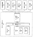
代表的な動作環境
図1及び対応する考察は、本発明の実施形態による適した動作環境の概説を提供することを目的とする。さらに後述するように、本発明の実施形態は、後述するように、ネットワーク化された構成又は結合構成を含め、様々なカスタマイズ可能な企業構成での1つ又は複数の動的モジュラー処理ユニットの使用を含む。
Exemplary Operating Environment FIG. 1 and corresponding discussion is intended to provide an overview of a suitable operating environment in accordance with an embodiment of the present invention. As will be further described below, embodiments of the present invention provide for the use of one or more dynamic modular processing units in various customizable enterprise configurations, including networked or combined configurations, as described below. including.
本発明の実施形態は1つ又は複数のコンピュータ可読媒体を含み、各媒体は、データ若しくはデータを操作するコンピュータ実行可能命令を含むように構成し得、又はそのようなデータ若しくはコンピュータ実行可能命令を含む。コンピュータ実行可能命令は、データ構造、オブジェクト、プログラム、ルーチン、又は様々な異なる機能を実行可能な汎用モジュラー処理ユニットに関連するか、若しくは限られた数の機能を実行可能な専用モジュラー処理ユニットに関連するような、1つ若しくは複数のプロセッサがアクセスし得る他のプログラムモジュールを含む。 Embodiments of the present invention include one or more computer-readable media, each medium may be configured to include data or computer-executable instructions for manipulating data, or such data or computer-executable instructions. Including. Computer-executable instructions relate to data structures, objects, programs, routines, or general-purpose modular processing units that can perform a variety of different functions, or to dedicated modular processing units that can perform a limited number of functions As well as other program modules accessible by one or more processors.
コンピュータ実行可能命令は、企業の1つ又は複数のプロセッサに、特定の機能又は機能群を実行させ、処理方法のステップを実施するプログラムコード手段の例である。さらに、特定の順序の実行可能命令は、そのようなステップの実施に使用し得る対応する動作の例を提供する。 Computer-executable instructions are examples of program code means that cause one or more processors of an enterprise to perform a particular function or group of functions and implement the steps of a processing method. Further, the specific order of executable instructions provides examples of corresponding operations that may be used to perform such steps.
コンピュータ可読媒体の例としては、ランダムアクセスメモリ(「RAM」)、読み取り専用メモリ(「ROM」)、プログラマブル読み取り専用メモリ(「PROM」)、消去可能プログラマブル読み取り専用メモリ(「EPROM」)、電気的に消去可能なプログラマブル読み取り専用メモリ(「EEPROM」)、コンパクトディスク読み取り専用メモリ(「CD−ROM」)、任意の固体状態記憶装置(例えば、フラッシュメモリ、スマートメディア等)、又は処理ユニットがアクセスし得るデータ若しくは実行可能命令を提供可能な任意の他の装置若しくは構成要素が挙げられる。 Examples of computer readable media include random access memory (“RAM”), read only memory (“ROM”), programmable read only memory (“PROM”), erasable programmable read only memory (“EPROM”), electrical Erasable programmable read-only memory (“EEPROM”), compact disc read-only memory (“CD-ROM”), any solid state storage device (eg, flash memory, smart media, etc.), or processing unit Any other device or component capable of providing the resulting data or executable instructions.
図1を参照すると、代表的な企業は、汎用又は専用処理ユニットとして使用し得るモジュラー処理ユニット10を含む。例えば、モジュラー処理ユニット10は、単独で利用してもよく、又はパーソナルコンピュータ、ノート型コンピュータ、個人情報端末(「PDA」)若しくは他のハンドヘルド装置、ワークステーション、ミニコンピュータ、メインフレーム、スーパーコンピュータ、マルチプロセッサシステム、ネットワークコンピュータ、プロセッサに基づく消費者装置、セルラ電話、スマート家電若しくは装置、制御システム等として、1つ若しくは複数の同様の処理ユニットと共に利用してもよい。複数の処理ユニットを同じ企業内で使用することにより、処理能力の増大が提供される。例えば、企業の各処理ユニットを特定のタスク専用にしてもよく、又は各処理ユニットがまとまって分散処理に参加してもよい。 Referring to FIG. 1, a typical enterprise includes a modular processing unit 10 that can be used as a general purpose or dedicated processing unit. For example, the modular processing unit 10 may be used alone or as a personal computer, notebook computer, personal information terminal ("PDA") or other handheld device, workstation, minicomputer, mainframe, supercomputer, It may be utilized with one or more similar processing units as a multiprocessor system, a network computer, a processor-based consumer device, a cellular phone, a smart home appliance or device, a control system, etc. The use of multiple processing units within the same enterprise provides increased processing capacity. For example, each processing unit of a company may be dedicated to a specific task, or each processing unit may participate in distributed processing together.
図1では、モジュラー処理ユニット10は、1つ又は複数のバス及び/又は相互接続12を含み、バス及び/又は相互接続12は、様々な構成要素を接続するように構成し得、2つ以上の構成要素間でデータを交換できるようにする。バス/相互接続12は、メモリバス、周辺バス、又は任意の様々なバス構造を使用するローカルバスを含む様々なバス構造の1つを含み得る。バス/相互接続12により接続される典型的な構成要素としては、1つ又は複数のプロセッサ14及び1つ又は複数のメモリ16が挙げられる。以下、「データ操作システム18」と呼ばれる論理、1つ若しくは複数のシステム、1つ若しくは複数のサブシステム、及び/又は1つ若しくは複数のI/Oインタフェースを使用して、他の構成要素もバス/相互接続12に選択的に接続し得る。さらに、論理、1つ若しくは複数のシステム、1つ若しくは複数のサブシステム、及び/又は1つ若しくは複数のI/Oインタフェースを使用して、他の構成要素を外部からバス/相互接続12に接続してもよく、且つ/又は他の構成要素が、1つ若しくは複数のモジュラー処理ユニット30及び/又はプロプライエタリ装置34等の論理、1つ若しくは複数のシステム、1つ若しくは複数のサブシステム、及び/又は1つ若しくは複数のI/Oインタフェースとして機能してもよい。I/Oインタフェースの例としては、1つ又は複数の大容量記憶装置インタフェース、1つ又は複数の入力インタフェース、1つ又は複数の出力インタフェース等が挙げられる。したがって、本発明の実施形態は、1つ若しくは複数のI/Oインタフェースを使用する能力及び/又は利用される論理若しくは他のデータ操作システムに基づいて製品の有用性を変更する能力を含む。
In FIG. 1, the modular processing unit 10 includes one or more buses and / or interconnects 12, which may be configured to connect various components. Allows data to be exchanged between components of Bus /
論理は、インタフェース、システムの部分、サブシステムに結びつけてもよく、且つ/又は特定のタスクの実行に使用されてもよい。したがって、論理又は他のデータ操作システムは、例えば、IEEE1394(ファイアワイヤ)を可能にし得、その場合、論理又は他のデータ操作システムはI/Oインタフェースである。代替又は追加として、モジュラー処理ユニットを別の外部システム又はサブシステムに結びつけられるようにする論理又は他のデータ操作システムを使用し得る。例えば、特別なI/O接続を含むこともあれば、含まないこともある外部システム又はサブシステム。代替又は追加として、外部I/Oに論理が関連付けられない論理又は他のデータ操作システムを使用し得る。本発明の実施形態は、車両のECU、油圧制御システム等の特殊論理及び特定のハードウェアの制御方法をプロセッサに通知する論理の使用も含む。さらに、本発明の実施形態が、論理、システム、サブシステム、及び/又はI/Oインタフェースを利用する沢山の異なるシステム及び/又は構成を包含することを当業者は理解しよう。 Logic may be tied to interfaces, system parts, subsystems, and / or used to perform specific tasks. Thus, a logic or other data manipulation system may enable, for example, IEEE 1394 (Firewire), in which case the logic or other data manipulation system is an I / O interface. Alternatively or additionally, logic or other data manipulation systems may be used that allow the modular processing unit to be linked to another external system or subsystem. For example, an external system or subsystem that may or may not include special I / O connections. Alternatively or additionally, logic or other data manipulation systems that do not have logic associated with external I / O may be used. Embodiments of the present invention also include the use of special logic such as vehicle ECUs, hydraulic control systems and the like and logic to notify the processor of specific hardware control methods. Moreover, those skilled in the art will appreciate that embodiments of the invention include many different systems and / or configurations that utilize logic, systems, subsystems, and / or I / O interfaces.
上に提供したように、本発明の実施形態は、1つ若しくは複数のI/Oインタフェースを使用する能力及び/又は利用される論理若しくは他のデータ操作システムに基づいて製品の有用性を変更する能力を含む。例えば、モジュラー処理ユニットが、1つ又は複数のI/Oインタフェースと、デスクトップコンピュータとして使用するように設計された論理とを含む個人計算システムの部分である場合、2つの標準RCAを介してアナログオーディオを取得し、IPアドレスにブロードキャストしたい音楽局へのオーディオ符号化を実行するフラッシュメモリ又は論理を含むように、論理又は他のデータ操作システムを変更することができる。したがって、モジュラー処理ユニットは、モジュラー処理システムのバックプレーン上のデータ操作システム(例えば、論理、システム、サブシステム、I/Oインタフェース等)に対して行われた変更により、コンピュータシステムではなく家電として使用されるシステムの部分であり得る。したがって、バックプレーン上のデータ操作システムの変更により、モジュラー処理ユニットの用途を変更することができる。したがって、本発明の実施形態は非常に適応性の高いモジュラー処理ユニットを含む。 As provided above, embodiments of the present invention change the usefulness of products based on the ability to use one or more I / O interfaces and / or the logic or other data manipulation system utilized. Including abilities. For example, if the modular processing unit is part of a personal computing system that includes one or more I / O interfaces and logic designed to be used as a desktop computer, analog audio via two standard RCAs And logic or other data manipulation systems can be modified to include flash memory or logic that performs audio encoding to music stations that want to obtain and broadcast to IP addresses. Thus, modular processing units can be used as consumer electronics rather than computer systems due to changes made to data manipulation systems (eg, logic, systems, subsystems, I / O interfaces, etc.) on the modular processing system backplane Can be part of the system Therefore, the usage of the modular processing unit can be changed by changing the data manipulation system on the backplane. Accordingly, embodiments of the present invention include a highly adaptive modular processing unit.
上に提供したように、処理ユニット10は、中央プロセッサ(又はCPU)等の1つ又は複数のプロセッサ14と、任意選択的に、特定の機能又はタスクを実行するように設計された1つ又は複数の他のプロセッサとを含む。通常、メモリ16、磁気ハードディスク、リムーバブル磁気ディスク、磁気カセット、光ディスク等のコンピュータ可読媒体に提供されるか、又は通信接続からの命令を実行するのはプロセッサ14であり、通信接続はコンピュータ可読媒体として見ることもできる。
As provided above, the processing unit 10 may be configured with one or
メモリ16は、データ若しくはデータを操作する命令を含むように構成し得るか、又はそのようなデータ若しくは命令を含み、バス/相互接続12を通してプロセッサ14がアクセス可能な1つ又は複数のコンピュータ可読媒体を含む。メモリ16は、例えば、情報を永久的に記憶するために使用されるROM20及び/又は情報を一時的に記憶するために使用されるRAM22を含み得る。ROM20は、モジュラー処理ユニット10のスタートアップ中等に通信を確立するために使用される1つ又は複数のルーチンを有する基本入/出力システム(「BIOS」)を含み得る。動作中、RAM22は、1つ又は複数のオペレーティングシステム、アプリケーションプログラム、及び/又はプログラムデータ等の1つ又は複数のプログラムモジュールを含み得る。
The memory 16 may be configured to include data or instructions for manipulating data, or one or more computer-readable media including such data or instructions and accessible to the
示されるように、本発明の少なくともいくつかの実施形態は、ユニットを様々な異なる用途で使用できるようにするよりロバストな処理ユニットを提供する非周辺ケースを含む。図1では、1つ又は複数の大容量記憶装置インタフェース(データ操作システム18として示される)を使用して、1つ又は複数の大容量記憶装置24をバス/相互接続12に接続し得る。大容量記憶装置24は、モジュラー処理ユニット10の周辺にあり、モジュラー処理ユニット10が大量のデータを保持できるようにする。大容量記憶装置の例としては、ハードディスクドライブ、磁気ディスクドライブ、テープドライブ、及び光ディスクドライブが挙げられる。
As shown, at least some embodiments of the present invention include a non-peripheral case that provides a more robust processing unit that allows the unit to be used in a variety of different applications. In FIG. 1, one or more mass storage device interfaces (shown as data manipulation system 18) may be used to connect one or more mass storage devices 24 to bus /
大容量記憶装置24は、磁気ハードディスク、リムーバブル磁気ディスク、磁気カセット、光ディスク、又は別のコンピュータ可読媒体と読み出し及び/又は書き込みを行い得る。大容量記憶装置24及び対応するコンピュータ可読媒体は、データ並びに/或いはオペレーティングシステム、1つ又は複数のアプリケーションプログラム、他のプログラムモジュール、又はプログラムデータ等の1つ又は複数のプログラムモジュールを含み得る実行可能命令の不揮発性記憶を提供する。そのような実行可能命令は、本明細書に開示される方法のステップを実施するプログラムコード手段の例である。 The mass storage device 24 may read from and / or write to a magnetic hard disk, a removable magnetic disk, a magnetic cassette, an optical disk, or another computer readable medium. Mass storage device 24 and corresponding computer-readable media may include data and / or one or more program modules such as an operating system, one or more application programs, other program modules, or program data. Provides non-volatile storage of instructions. Such executable instructions are an example of program code means for performing the steps of the methods disclosed herein.
データ操作システム18を利用して、1つ又は複数の対応する周辺I/O装置26を通して、データ及び/又は命令をモジュラー処理ユニット10と交換できるようにし得る。周辺I/O装置26の例としては、キーボード等の入力装置及び/又はマウス、トラックボール、ライトペン、スタイラス若しくは他のポインティングデバイス、マイクロフォン、ジョイスティック、ゲームパッド、パラボラアンテナ、スキャナ、カムコーダ、デジタルカメラ、センサ等の代替の入力装置、並びに/或いはモニタ若しくは表示画面、スピーカ、プリンタ、制御システム等の出力装置が挙げられる。同様に、周辺I/O装置26をバス/相互接続12に接続するために使用し得る専用論理に結合されたデータ操作システム18の例としては、シリアルポート、パラレルポート、ゲームポート、ユニバーサルシリアルバス(「USB」)、ファイアワイヤ(IEEE1394)、無線受信器、ビデオアダプタ、オーディオアダプタ、パラレルポート、無線送信器、任意の並列又は直列化I/O周辺装置又は別のインタフェースが挙げられる。
The
データ操作システム18は、1つ又は複数のネットワークインタフェース28を介して情報を交換できるようにする。ネットワークインタフェース28の例としては、情報を処理ユニット間で交換できるようにする接続、ローカルエリアネットワーク(「LAN」)に接続するためのネットワークアダプタ若しくはモデム、無線リンク、又はインターネット等の広域ネットワーク(「WAN」)に接続するための別のアダプタが挙げられる。ネットワークインタフェース28は、モジュラー処理ユニット10に組み込まれてもよく、又はモジュラー処理ユニット10の周辺にあってもよく、LAN、無線ネットワーク、WAN、及び/又は処理ユニット間の任意の接続に関連付け得る。
データ操作システム18は、モジュラー処理ユニット10が1つ又は複数の他のローカル又はリモートモジュラー処理ユニット30又はコンピュータ装置と情報を交換できるようにする。モジュラー処理ユニット10とモジュラー処理ユニット30との接続は、ハードワイヤードリンク及び/又は無線リンクを含み得る。したがって、本発明の実施形態は、直接バス−バス接続を含む。これにより、大規模なバスシステムの作成が可能になる。これは、企業の直接バス−バス接続により、現在知られているハッキングもなくす。さらに、データ操作システム18は、モジュラー処理ユニット10が、1つ若しくは複数のプロプライエタリI/O接続32及び/又は1つ若しくは複数のプロプライエタリ装置34と情報を交換できるようにする。
処理ユニットがアクセス可能なプログラムモジュール又はその部分は、リモートメモリ記憶装置に記憶し得る。さらに、ネットワーク化されたシステム又は結合構成では、モジュラー処理ユニット10は、分散計算環境に参加し得、分散計算環境では、機能又はタスクが複数の処理ユニットにより実行される。或いは、結合構成/企業の各処理ユニットは、特定のタスク専用であってもよい。したがって、例えば、企業の1つの処理ユニットはビデオデータ専用であり、それにより、従来のビデオカードに取って代わることができ、従来の技法よりも優れたそのようなタスクを実行する増大した処理能力を提供する。 Program modules accessible by the processing unit or portions thereof may be stored in a remote memory storage device. Further, in a networked system or combined configuration, modular processing unit 10 may participate in a distributed computing environment where functions or tasks are performed by multiple processing units. Alternatively, each processing unit of the combined configuration / enterprise may be dedicated to a specific task. Thus, for example, one processing unit in an enterprise is dedicated to video data, which can replace conventional video cards, and increased processing power to perform such tasks better than conventional techniques. I will provide a.
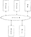
本発明を多くの種類のコンピュータシステム構成を有するネットワーク化された計算環境で実施し得ることを当業者は理解するが、図2は、ネットワークを介してサーバに接続されたクライアントを含むネットワーク化環境での本発明の実施形態を表す。図2は、ネットワークに接続された2つのクライアントを含む実施形態を示すが、代替の実施形態は、ネットワークに接続された1つのクライアント又はネットワークに接続された多数のクライアントを含む。さらに、本発明による実施形態は、ネットワークに接続された世界全体にわたる多数のクライアントも含み、この場合、ネットワークはインターネット等の広域ネットワークである。 Those skilled in the art will appreciate that the present invention may be implemented in a networked computing environment having many types of computer system configurations, but FIG. 2 illustrates a networked environment that includes a client connected to a server via a network. 1 represents an embodiment of the present invention. Although FIG. 2 illustrates an embodiment that includes two clients connected to a network, an alternative embodiment includes one client connected to the network or multiple clients connected to the network. In addition, embodiments according to the present invention also include a number of global clients connected to the network, where the network is a wide area network such as the Internet.
電源
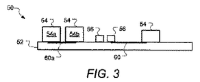
本発明のいくつかの態様は電源に関する。上述したように、多くの従来の電源設計は多くの場合、あまり空間効率的ではない。電源は、複数の電子構成要素を含むことができ、これらの電子構成要素は能動的構成要素及び受動的構成要素を含むことができる。能動的構成要素は、スイッチ(例えば、双極トランジスタ、電界効果トランジスタ等)、調整器、比較器等の部品を含む。受動的構成要素は、抵抗、インダクタ、コンデンサ等の部品を含む。電子構成要素は通常PCBに搭載され、PCB上のトレースを通して相互接続される。通常、電子構成要素はPCBの片側のみに搭載される。これは、電子産業ではコスト考慮事項から望ましいと見られている。いくつかの場合、受動的構成要素(例えば、小型コンデンサ又は小型抵抗)は往々にして、基板の逆側に配置される。例えば、図3は、全体的に50で示される電源を示し、PCB52は、PCB(又は他の回路基板)の片側58に搭載された複数の構成要素54及び56を有する。構成要素は、能動的構成要素54及び受動的構成要素56を含むことができる。構成要素の相互接続はトレース60(例えば、非導電基板に取り付けられるか、又は堆積した導電材料)により提供される。PCBは、例えば、複数層のトレース(図示せず)を提供する多層PCBであることができる。
Power Supply Some aspects of the present invention relate to a power supply. As mentioned above, many conventional power supply designs are often not very space efficient. The power supply can include a plurality of electronic components, which can include active components and passive components. Active components include components such as switches (eg, bipolar transistors, field effect transistors, etc.), regulators, comparators, and the like. Passive components include components such as resistors, inductors and capacitors. Electronic components are usually mounted on a PCB and interconnected through traces on the PCB. Usually, the electronic components are mounted only on one side of the PCB. This is seen as desirable in the electronics industry due to cost considerations. In some cases, passive components (eg, small capacitors or small resistors) are often placed on the opposite side of the substrate. For example, FIG. 3 shows a power supply generally designated 50, and the
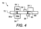
本発明のいくつかの実施形態による小型化電源を図4に示す。従来の電源とは対照的に、小型化電源70は、PCB72の両側に配置された能動的構成要素54を含むことができる。したがって、いくつかの能動的構成要素は、いくつかの実施形態では、互いの真逆に配置することができる。他の実施形態では、能動的構成要素は互いに対向し、部分的に重なり得る。受動的構成要素56もPCBの片側又は両側に配置することができる。トレース60及びバイア80は構成要素を相互接続することができる。
A miniaturized power source according to some embodiments of the present invention is shown in FIG. In contrast to conventional power supplies,
PCB72の両側に構成要素を搭載することにより、いくつかの利点を得ることができる。例えば、構成要素の相互接続距離を低減することができる。例えば、第1の構成要素54a及び第2の構成要素54bを考えると、これらの構成要素は、PCBの同じ側にある場合、図3に示されるよりも大幅に近くに配置することはできない。例えば、構成要素のサイズ許容差及びピックアンドプレース機のアクセスを可能にするために、いくらかの離間が通常、構成要素間に必要とされる。したがって、第1の構成要素の端子を第2の構成要素の端子に相互接続するトレース60aは一般に、構成要素の水平寸法以上の長さを有さなければならない。例えば、約0.64cm(約0.25インチ)の水平長さを有する2つの構成要素を相互接続するには、トレースは少なくとも約0.64cm(約0.25インチ)の長さでなければならない。
By mounting components on both sides of the
対照的に、構成要素54a、54bがPCB72の両側に互いに逆に配置される場合、トレース長を大幅に短くすることができる。例えば、構成要素は端子が互いに真逆になり、トレース長を本質的に、構成要素を互いに相互接続するバイア80aの長さにする(例えば、パッドにより追加の長さがあり得る)ように配置することができる。したがって、PCB72が約0.13cm(約0.05インチ)の厚さを有する場合、トレース長は約0.13cm(約0.05インチ)の長さである−約1/5の低減。
In contrast, if the
本発明のいくつかの実施形態において提供されるトレース長の低減は、複数の利点を提供することができる。例えば、理想的な電気相互接続はゼロ抵抗、ゼロ容量、及びゼロインダクタンスを有するが、実際のトレースはいくらかの寄生抵抗、寄生容量、及び寄生インダクタンス(RLC)を示す。トレースのRLCは様々なパラメータ(例えば、基板の厚さ、導電材料の厚さ、絶縁基板の誘電率、他のトレースの近さ等)の関数であるが、トレース長への寄生RLCの大きな依存がある。一般に、寄生RLCはトレース長に伴って線形に増大する。したがって、トレース長を低減することにより、寄生RLCを低減することができ、寄生RLCの低減により、電気接続は理想的な(例えば、ゼロRLC)相互接続により類似して挙動することができる。いくつかの場合、寄生RLCの低減には、構成要素値の調整が必要であり得る。例えば、回路設計は特定量のインダクタンスを必要とし得る。片面設計では、この所要インダクタンスは、部分的には構成要素及び部分的にはPCB52の寄生インダクタンスにより提供し得る。両面設計では、PCB72により提供される寄生インダクタンスが低減するため、構成要素インダクタンスが低減され得る。別の例として、片面設計では、構成要素値は、寄生RLCを補償する必要があり得、したがって、両面設計では、寄生RLCの低減により、構成要素値を低減するか、又は構成要素を全体的になくし得る。
The trace length reduction provided in some embodiments of the present invention can provide several advantages. For example, an ideal electrical interconnect has zero resistance, zero capacitance, and zero inductance, but actual traces exhibit some parasitic resistance, parasitic capacitance, and parasitic inductance (RLC). Trace RLC is a function of various parameters (eg, substrate thickness, conductive material thickness, dielectric constant of insulating substrate, proximity of other traces, etc.), but large dependence of parasitic RLC on trace length There is. In general, parasitic RLC increases linearly with trace length. Thus, reducing the trace length can reduce parasitic RLC, and by reducing parasitic RLC, electrical connections can behave more like an ideal (eg, zero RLC) interconnect. In some cases, reduction of parasitic RLC may require adjustment of component values. For example, a circuit design may require a certain amount of inductance. In a single-sided design, this required inductance can be provided in part by the parasitic inductance of the component and in part by the
トレース長低減の別の利点は、雑音放射の低減及び雑音の影響の受けやすさの低減である。電気相互接続は、放射性及び非放射性電磁結合の両方を通して雑音を放射し得る。一般に、雑音結合の量は、電磁相互接続が長いほど増大する。例えば、長いトレースほど、互いの間に高い相互容量又はインダクタンスを有し、電磁場を通して高い結合を提供し得る。長いトレースほど、アンテナとして効果的に動作し、伝播する電磁波を通してエネルギーを放射するか、又は隣接するトレースからエネルギーを収集し得る。したがって、トレース長を低減することにより、雑音結合を低減することもできる。 Another advantage of reduced trace length is reduced noise emissions and reduced noise susceptibility. Electrical interconnects can radiate noise through both radiative and non-radiative electromagnetic coupling. In general, the amount of noise coupling increases with longer electromagnetic interconnections. For example, longer traces may have higher mutual capacitance or inductance between each other and provide higher coupling through the electromagnetic field. Longer traces can operate more effectively as antennas and radiate energy through propagating electromagnetic waves or collect energy from adjacent traces. Therefore, noise coupling can also be reduced by reducing the trace length.
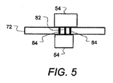
いくつかの場合、両面設計でのトレース長は、トレース長が長い場合には必要な遮蔽をなくすことができる十分に短くすることができる。他の場合、遮蔽により失われる面積を大幅に低減することができる。例えば、図5は、PCB72の両側に搭載された2つの構成要素54の間の遮蔽接続を示す。遮蔽接続は、2つの構成要素を電気的に接続し、複数の遮蔽構造84で囲まれた信号導体82を備える。遮蔽構造は、例えば、接地板に接続するバイア及び/又はトレースを含むことができる。遮蔽構造が全体的に構成要素のフットプリント内に含まれ、したがって、構成要素によりすでに覆われた箇所を超える追加のいかなるPCB面積も必要ないことが分かる。遮蔽接続は、ピックアップ雑音の影響を特に受けやすい電気接続及び特に雑音を放射しがちの電気接続に使用することができる。図5に示される遮蔽接続は垂直方向にある(信号導体のバイア及び遮蔽構造を使用して)が、遮蔽接続は水平に提供することもでき(信号導体のトレース及び遮蔽構造を使用して)、又は両方の組み合わせを使用して提供することもできる。
In some cases, the trace length in a double-sided design can be short enough to eliminate the necessary shielding if the trace length is long. In other cases, the area lost by shielding can be significantly reduced. For example, FIG. 5 shows a shield connection between two
トレース長短縮のさらなる利点は、トレースが消費する基板面積量の低減である。この面積は、様々な有利な方法で使用することができる。例えば、トレース幅を増大させることができる。一般に、トレース幅が広いほど、低い抵抗及びインダクタンスを提供することができ、高い電流処理能力が提供される。 A further advantage of shortening the trace length is a reduction in the amount of substrate area consumed by the trace. This area can be used in various advantageous ways. For example, the trace width can be increased. In general, wider trace widths can provide lower resistance and inductance, providing higher current handling capability.
電源は、相互接続面を効果的に利用することもできる。例えば、相互接続面は、PCB72の外層又は内層に配置された導電材料の本質的な連続面(例えば、ばか穴を除き、画定された二次元面積範囲にわたって連続する)からなり得る。例えば、接地面を使用して、2つ以上の構成要素の接地端子を一緒に接続することができる。別の例として、電力面を使用して、2つ以上の構成要素の電力端子を一緒に接続することができる。相互接続面は、面に結びつけられた構成要素間に低抵抗且つ低インダクタンスの相互接続を提供するため、有利であり得る。必要な場合、穴をプランに提供して、面に電気的に接続せずに、面を貫通するバイア(例えば、信号相互接続の)の隙間を提供することができる。 The power supply can also effectively utilize the interconnection surface. For example, the interconnect surface may consist of an essentially continuous surface of conductive material disposed on the outer or inner layer of PCB 72 (eg, continuous over a defined two-dimensional area range, excluding the hole). For example, a ground plane can be used to connect the ground terminals of two or more components together. As another example, a power plane can be used to connect power terminals of two or more components together. The interconnect surface can be advantageous because it provides a low resistance and low inductance interconnect between components associated with the surface. If necessary, holes can be provided in the plan to provide via (eg, signal interconnect) gaps through the surface without electrical connection to the surface.
いくつかの場合、単一点で互いに相互接続される1つ又は複数の分割面を提供することが有利であり得る。例えば、図6は、PCB92が電源部分94及び動作回路部分96を含む電子システムのPCB設計90を示す。複数の分割面セクション98、100、及び102が提供される。分割面は、例えば、切り欠き部分又はエッチング部分を有して分割面を画定するPCBの外層又は内層に配置された導電層であり得る。動作回路は分割面セクション102を備え、このセクションは、動作回路の下で連続する(バイアばか穴104を除く)。電源部分は2つの分割面セクション98及び100を備える。面部分のそれぞれは、単一接続点106を介して互いに接続する。複数の分割面の使用は、電源内で生成される雑音を電源内に閉じ込め、電源の雑音の影響を受けやすい部分(例えば、面98の上下に配置される)を電源の雑音生成部分(例えば、面100の上下に配置される部分)から分離するために有利であり得る。
In some cases it may be advantageous to provide one or more split surfaces that are interconnected to each other at a single point. For example, FIG. 6 shows a
コンデンサの量及び種類を最適化することにより、電源のさらなる小型化を得ることができる。コンデンサは電源でいくつかの目的を果たすことができる。コンデンサは、電源のサイクル間に電荷貯蔵を提供することができる(例えば、線形供給では交流電流入力のサイクル又は切り替え電源での切り替えサイクル中)。コンデンサは、エネルギー貯蔵を提供して、サージ電流需要(例えば、発生が早すぎて調整器が応答できない)を満たすこともできる。コンデンサは雑音フィルタリング(例えば、接地への雑音信号の分路)を提供することもできる。通常、電源には、通常の動作条件下で電荷を貯蔵するために必要な量を超える大量の容量が設計される。この過度の容量は、部分的にはコンデンサの有効性を制限する大きなコンデンサの非理想的な応答(例えば、等価直列抵抗)により提供される。 By optimizing the amount and type of capacitors, further miniaturization of the power supply can be obtained. Capacitors can serve several purposes in the power supply. Capacitors can provide charge storage between cycles of the power supply (eg, in a linear supply, during an alternating current input cycle or during a switching cycle with a switched power supply). Capacitors can also provide energy storage to meet surge current demand (e.g., too early to occur and the regulator cannot respond). The capacitor can also provide noise filtering (eg, shunting the noise signal to ground). Typically, power supplies are designed with large capacities that exceed those required to store charge under normal operating conditions. This excessive capacitance is provided in part by the large capacitor's non-ideal response (eg, equivalent series resistance) that limits the effectiveness of the capacitor.
対照的に、種類を混ぜたコンデンサを使用することにより、提供される全静電容量を低減できることが本発明者等により発見されている。例えば、全静電容量要件は、電源により供給される動作回路の要件及び電源の特徴に基づいて決定される。次に、全静電容量要件は、異なる種類のコンデンサに分けることができる。いくつかの小さく、等価直列抵抗(ESR)が低いコンデンサを提供することができる。低ESRコンデンサは、高速負荷変化に素早く応答することができるが、限られた電荷貯蔵能力を提供する。しかし、全静電容量要件の提供にすべて低ESRコンデンサを使用することは、低ESRコンデンサのサイズ及びコストにより非実用的である。したがって、より高いESRを有する追加のコンデンサを提供することができる。ESRのより高いコンデンサは、応答が遅いが、負荷変動が低ESRコンデンサの能力を超える場合に応答することができる。したがって、全静電容量要件は、部分的には低ESRコンデンサ及び部分的には高ESRコンデンサにより満たすことができる。所望であれば、全静電容量要件を2つ以上の種類のコンデンサに分けることができる。特定の例として、1ファラッドの全静電容量要件を低ESRコンデンサ100ミリファラッド、中ESRコンデンサ400ミリファラッド、及び高ESRコンデンサ0.5ファラッドに分けることができる。
In contrast, the present inventors have discovered that the total capacitance provided can be reduced by using mixed capacitor types. For example, the total capacitance requirement is determined based on the requirements of the operating circuit supplied by the power source and the characteristics of the power source. Second, the total capacitance requirement can be divided into different types of capacitors. Several small, low equivalent series resistance (ESR) capacitors can be provided. Low ESR capacitors can respond quickly to fast load changes, but provide limited charge storage capability. However, using all low ESR capacitors to provide full capacitance requirements is impractical due to the size and cost of the low ESR capacitors. Thus, an additional capacitor having a higher ESR can be provided. Capacitors with higher ESR are slow to respond, but can respond when load variations exceed the capabilities of low ESR capacitors. Thus, the total capacitance requirement can be met in part by low and high ESR capacitors. If desired, the total capacitance requirement can be divided into two or more types of capacitors. As a specific example, the total capacitance requirement of 1 Farad can be divided into a
全静電容量要件をそのようにして分けることにより、従来の設計と比較して全静電容量を低減することができ、それにより、使用される基板面積の低減が提供される。さらに、すべての中又は高ESRコンデンサを使用する従来の設計と比較して、必要な全静電容量を一般に低減できることが観測されている。 By so dividing the total capacitance requirement, the total capacitance can be reduced compared to conventional designs, thereby providing a reduction in the substrate area used. Furthermore, it has been observed that the overall required capacitance can generally be reduced compared to conventional designs that use all medium or high ESR capacitors.
小型化電源の製造は、図7に示されるフローチャートによるものを含め、任意の適した様式で進めることができる。方法110はボックス112で開始することができ、電源の設計概略が得られる。例えば、設計概略は技術者が作成することができる。設計概略は、例えば、構成要素の製造業者により提供される基準設計に基づいてもよく、又はカスタマイズされた設計であってもよい。
The manufacture of the miniaturized power source can proceed in any suitable manner, including by the flowchart shown in FIG. The
設計概略は、電源を構成する構成要素を定義する部品リストと、構成要素間の相互接続を定義するネットリストとを含むことができる。設計概略は電子形態であることができる。設計概略は、業界標準ファイル形式等のコンピュータ支援設計(「CAD」)システムが使用可能な形態であることができる。 The design outline can include a parts list that defines the components that make up the power supply and a netlist that defines the interconnections between the components. The design outline can be in electronic form. The design outline can be in a form that can be used by a computer-aided design (“CAD”) system, such as an industry standard file format.
ボックス114及び116は、複数ののうちの第1及び第2の構成要素の、PCBの第1及び第2の側での位置を選択することにより、方法110を続けることができることを示す。PCBのレイアウトは、CADレイアウトツールを使用して決定することができる。CADレイアウトツールを使用して、PCB上の構成要素の位置を定義することができる。例えば、電子構成要素のうちの第1の構成要素は、PCBの第1の側に位置決めし、電子構成要素のうちの第2の構成要素は、PCBの第2の側に位置決めすることができる。電子構成要素のうちの第2の構成要素の位置は、これより説明するように、電子構成要素の第1の構成要素の位置に関連し得る。
電子構成要素を位置決めする場合、様々な側面を考慮することができる。構成要素は、トレース長を最小化するように、互いに対して位置決めすることができる。トレース長の相対的な重要度も同様に考慮することができ、重要なトレース(例えば、雑音の影響を受けやすいか、又は雑音を放射する可能性がかなり高い相互接続に対応するトレース)を、あまり重要ではないトレースを長くすることを犠牲にして短く保つという妥協がなされる。例えば、感知線は雑音の影響を特に受けやすい傾向を有するため、他のトレースから離すか、又は遮蔽することができる。特定の例として、電源内の回路を感知して、過電流及び過/不足電圧状況を検出することにより、感知線を使用することができる。感知線による雑音ピックアップは、スプリアス検出に繋がり、電源の望ましくない遮断に繋がるおそれがある。 Various aspects can be considered when positioning electronic components. The components can be positioned relative to each other so as to minimize the trace length. The relative importance of the trace length can be taken into account as well, and important traces (for example, traces corresponding to interconnects that are susceptible to noise or are very likely to emit noise), A compromise is made to keep the less important traces short at the expense of longer. For example, sense lines tend to be particularly susceptible to noise and can be kept away from other traces or shielded. As a specific example, sensing lines can be used by sensing circuitry in the power supply to detect overcurrent and over / undervoltage conditions. Noise pick-up due to the sensing line can lead to spurious detection and can lead to an undesirable shutdown of the power supply.
構成要素は、基板の両側に互いに対して位置決めして、バイアに複数の目的を果たさせることができる。例えば、従来の片面PCBは多くの場合、バイアを含み、PCBの上側のトレースと下側のトレース(及び存在する場合には中間層のトレース)の間に接続を提供する。小型化電源では、構成要素をPCBの逆側に位置決めして、バイアに複数の目的を果たさせることもできる。例えば、上側のトレースを下側のトレースに接続するために使用されるバイアは、下側の部分に接続するために使用することもできる。 The components can be positioned relative to each other on both sides of the substrate to allow the via to serve multiple purposes. For example, conventional single-sided PCBs often include vias and provide a connection between the upper and lower traces (and intermediate layer traces, if any) of the PCB. In a miniaturized power supply, the components can be positioned on the opposite side of the PCB, allowing the via to serve multiple purposes. For example, a via used to connect the upper trace to the lower trace can also be used to connect to the lower portion.
部品を第1の側に対して第2の側に位置決めする場合、部品の位置の配慮は、排他的に相互接続長に焦点を合わせる必要はない。例えば、雑音の影響を受けやすい構成要素は、雑音生成構成要素から離すことができる。 When positioning the component on the second side relative to the first side, consideration of the position of the component need not exclusively focus on the interconnect length. For example, noise sensitive components can be separated from noise generating components.
小型化電源をレイアウトする場合、位置の選択は、三次元位置決めタスクとして見ることができる。換言すれば、構成要素の位置は、X、Y、及びZ寸法で定義することができ、X及びYはPCBの横寸法に対応し(PCBにより定義される平面内、例えば、「左/右」)に対応し、Z寸法はPCBでの垂直寸法(PCBにより定義される平面に垂直、例えば、「上」及び「下」)に対応する。位置は、PCBでの基準点に対して定義することができる。これは、単にX及びY寸法で位置決めする従来の片面PCB設計とは対照的である。 When laying out a miniaturized power source, position selection can be viewed as a three-dimensional positioning task. In other words, component positions can be defined by X, Y, and Z dimensions, where X and Y correspond to the lateral dimensions of the PCB (in the plane defined by the PCB, eg, “left / right )) And the Z dimension corresponds to the vertical dimension on the PCB (perpendicular to the plane defined by the PCB, eg, “up” and “down”). The position can be defined relative to a reference point on the PCB. This is in contrast to conventional single-sided PCB designs that are simply positioned in the X and Y dimensions.
構成要素が位置決めされると、ボックス118は、相互接続を定義できることを示す。例えば、相互接続は、パッド(構成要素の端子への電気接続のため)、トレース、及びバイアを含むことができる。パッド、トレース、及びバイアの位置は、基準点に対して定義することができる。相互接続の配線は、例えば、自動配線ツールを使用して実行することができる。パッド、トレース、及びバイアの位置を定義するPCBレイアウトは、CADシステムから電子形態で提供することができる。例えば、PCBレイアウトは、PCBの組み立てに使用可能な業界標準形式で定義することができる。PCBは、PCBレイアウトに従って組み立てることができる。ボックス120に示されるように、電源は、構成要素をPCBに搭載して電気的に接続することにより、組み立てられたPCBから構築することができる。 Once the component is positioned, box 118 indicates that an interconnection can be defined. For example, interconnects can include pads (for electrical connection to component terminals), traces, and vias. Pad, trace, and via locations can be defined relative to a reference point. Interconnect wiring can be performed using, for example, an automatic wiring tool. A PCB layout defining the location of pads, traces and vias can be provided in electronic form from a CAD system. For example, a PCB layout can be defined in an industry standard format that can be used to assemble a PCB. The PCB can be assembled according to the PCB layout. As shown in box 120, the power source can be constructed from the assembled PCB by mounting components on the PCB and electrically connecting them.
本発明のいくつかの実施形態による小型化電源は、消費面積の低減において利点を提供する。例えば、いくつかの実施形態では、PCB面積は、従来の片面設計での約10.2cm2(約4平方インチ)から、両面設計での約2.5cm2(約1平方インチ)に低減した。 Miniaturized power sources according to some embodiments of the present invention provide advantages in reducing consumption area. For example, in some embodiments, the PCB area has been reduced from about 10.2 cm 2 (about 4 square inches) in a conventional single-sided design to about 2.5 cm 2 (about 1 square inch) in a double-sided design. .
驚くことに、性能向上での追加の利点も、いくつかの実施形態において観測された。例えば、トレース長の低減及びトレース間の相互作用の低減により、向上した雑音性能が観測された。特に、小型化電源の調整及び出力雑音の安定性は、従来の片面PCB設計と比較して大幅に向上することが観測された。一般に、スペース及び性能の向上した効率は、PCBの両面に能動的部品を配置することに関連する追加の製造(及び修理)コストを相殺するのに十分であり得る。 Surprisingly, additional benefits in performance enhancement have also been observed in some embodiments. For example, improved noise performance was observed due to reduced trace length and reduced interaction between traces. In particular, it has been observed that the adjustment of the miniaturized power supply and the stability of the output noise are significantly improved compared to the conventional single-sided PCB design. In general, improved efficiency in space and performance may be sufficient to offset the additional manufacturing (and repair) costs associated with placing active components on both sides of the PCB.
これより理解されるように、本開示による小型化電源は、面積効率がより高い高性能電源を提供するのに役立ち得る。そのような電源は、コンパクト計算システム、埋め込みコンピュータ、ラップトップコンピュータ、及び同様の用途等の面積が制限される用途でとくに有用であり得る。 As will be appreciated, miniaturized power sources according to the present disclosure can help provide a high performance power source that is more area efficient. Such a power source can be particularly useful in area limited applications such as compact computing systems, embedded computers, laptop computers, and similar applications.
したがって、本明細書において考察するように、本発明の少なくともいくつかの態様は電源を小型化する技法を含む。特に、本発明の少なくともいくつかの態様は、PCBの面積利用を効率的にする小型化電源に関する。 Thus, as discussed herein, at least some aspects of the present invention include techniques for miniaturizing power supplies. In particular, at least some aspects of the present invention relate to miniaturized power supplies that make efficient use of PCB area.
メモリ
本発明のいくつかの態様は、コンピュータ装置又はシステムでのメモリ性能を最適化するシステム及び方法に関する。さらに、本発明のいくつかの態様は、回路基板上のメモリレイアウトを小型化し最適化するシステム及び方法に関する。
Memory Some aspects of the present invention relate to systems and methods for optimizing memory performance in a computer device or system. Furthermore, some aspects of the invention relate to systems and methods for miniaturizing and optimizing memory layout on a circuit board.
メモリコントローラ132と、1組8つのメモリ素子134、136、138、140、142、144、146、及び148(M1〜M8とも記される)とを有するメモリシステム130のPCBレイアウトを示す図8をこれより参照する。8つのメモリ素子のそれぞれは、PCB150にはんだ付けされるか、又は他の様式で電気的に直接結合される。4つのメモリ素子M1、M3、M5、及びM7はPCB150aの上面にはんだ付けされ、4つの他のメモリ素子M2、M4、M6、及びM8は下面150bにはんだ付けされる(直接示されない)(これらの素子は、PCB150の下面150bにあることを表すために点線で示される)。この直接接続は、1つ又は複数の接続スロットを有するDIMMを有する特定の従来のメモリ接続とは異なる。それらの素子では、メモリはメモリカードにはんだ付けされ、メモリカードがDIMMに挿入された。したがって、代表的な実施形態は、この間接的な接続をなくし、それにより、DIMM及び対応する回路の必要性がなくなる。
FIG. 8 shows a PCB layout of a
DIMMを除去することにより、メモリ素子をメモリコントローラ132のはるかに近傍に配置することができる。したがって、少なくともいくつかの実施形態では、各メモリ素子の部分は、メモリコントローラ152から約6.4cm(約2.5インチ)以下の距離152以内に配置される。この距離152により、メモリシステムをハンドヘルドコンピュータシステム及び小型コンピュータシステム等のよりコンパクトな装置に配置できるようにする、よりコンパクトで最適化されたPCBレイアウトが可能である。さらに、いくつかの実施形態では、メモリ素子全体は、メモリコントローラ132から約6.4cm(約2.5インチ)以下の距離154以内に配置される。
By removing the DIMM, the memory element can be placed much closer to the
述べたように、メモリ素子M1〜M8はPCBに直接はんだ付けされる。はんだ付けされたメモリ素子は、DIMMソケットよりも強化された耐衝撃性及び耐ショック性を有し、したがって、より厳しい環境に組み込むことができるロックタイトシステムを提供しながら、装置故障の可能性を低減する。メモリが、DIMMスロットに挿入されるメモリカードにはんだ付けされる場合、メモリカードとスロットの接続は弱く、コンピュータシステム全体の多用途性を低減する。したがって、はんだ付けされたメモリ素子を有する本システムでは、大きな衝撃に耐えるとともに、オートモバイルコンピュータシステム等の従来のデスクトップコンピュータシステムよりも厳しい環境に耐えるように設計されたコンピュータ装置又はシステムにPCB全体を組み込むことができる。 As stated, memory elements M1-M8 are soldered directly to the PCB. Soldered memory elements have enhanced shock and shock resistance over DIMM sockets, thus reducing the possibility of device failure while providing a Loctite system that can be integrated into harsh environments To do. When the memory is soldered to a memory card that is inserted into a DIMM slot, the connection between the memory card and the slot is weak, reducing the versatility of the entire computer system. Thus, in this system with soldered memory elements, the entire PCB can be placed on a computer device or system that is designed to withstand large impacts and tougher environments than conventional desktop computer systems such as auto mobile computer systems. Can be incorporated.
物理的な強度及び最適化されたレイアウトに加えて、はんだ付けされたメモリ素子は、スケーラブルメモリシステムの不確実性を除去する。メモリ素子M1〜M8をPCB150に固定することにより、システム設計者はメモリ素子性能を最適化することができ、メモリ素子をより高いレベルで実行させ、したがって、コストを増大せずにシステム性能が増大する。
In addition to physical strength and optimized layout, soldered memory elements remove the uncertainty of scalable memory systems. By fixing memory elements M1-M8 to
さらに、メモリ素子コストが下がりつつあるという最近の傾向に鑑みて、少なくともいくつかの実施形態では、DIMMコネクタソケットを使用してメモリ拡張性を提供するのではなく、PDBで使用可能な最大メモリを増大することが経済的に実現可能である。少なくともいくつかの実施形態では、今では、ホストコンピュータシステムが直接使用可能な予測可能な最大システムメモリを装置にまず設置することが実現可能である。これにより、拡張可能なDIMM、そのような部品のコスト、そのような部品のサイズ、並びに対応する設計不確実性の必要がなくなる。 Furthermore, in view of the recent trend of decreasing memory device costs, at least some embodiments provide the maximum memory available in the PDB, rather than providing memory expandability using DIMM connector sockets. Increasing is economically feasible. In at least some embodiments, it is now feasible to first install in the device a predictable maximum system memory that can be used directly by the host computer system. This eliminates the need for expandable DIMMs, the cost of such parts, the size of such parts, and the corresponding design uncertainty.
引き続き図8を参照すると、代表的な実施形態では、システム130は、メモリコントローラ132の近傍でPCB150に直接はんだ付けされた複数のメモリ素子を含む。いくつかの実施形態では、メモリ素子は、PCB150の上面150a及び下面150bの両方に配置されて、PCBスペースを最大化する。したがって、いくつかの実施形態では、PCBの上面150aのメモリ素子は、下面150bにあるメモリ素子の真上にある。他の実施形態では、上面のメモリ素子は、下面のメモリ素子と互い違いになる。示されるように、メモリ素子は直線に配置される。しかし、他の実施形態では、メモリ素子は、複数の線に配置されたメモリコントローラ132の周囲に配置された群にクラスタ化され、又はメモリコントローラ132の近傍に他の様式で配置される。
With continued reference to FIG. 8, in the exemplary embodiment,
いくつかの実施形態では、個々のメモリ素子M1〜M8は、組み合わせてパーソナルコンピュータのメインメモリ(「RAM」)を形成し得るDRAMメモリである。DRAMは、データの各ビットを集積回路内の別個のコンデンサに記憶するランダムアクセスメモリの一種である。実際のコンデンサは電荷が漏れるため、コンデンサ電荷が周期的にリフレッシュされない限り、情報は最終的には消えていく。このリフレッシュ要件により、SRAM及び他の静的メモリとは対照的なのが動的メモリであり、DRAMメモリ素子は非常に小型に製造することができ、PCBレイアウトの最適化及び小さなPCBフットプリントを可能にする。他の実施形態では、メモリ素子はSRAM、TRAM、ZRAM、及び/又はTTRAMメモリを含む。なお他の実施形態では、システムは、EEPROMメモリ又はフラッシュメモリ等の不揮発性メモリ素子を含む。 In some embodiments, the individual memory elements M1-M8 are DRAM memories that can be combined to form the main memory ("RAM") of a personal computer. DRAM is a type of random access memory that stores each bit of data in a separate capacitor in an integrated circuit. Since the actual capacitor leaks charge, information will eventually disappear unless the capacitor charge is periodically refreshed. Due to this refresh requirement, dynamic memory is in contrast to SRAM and other static memories, DRAM memory devices can be made very small, allowing PCB layout optimization and small PCB footprint. To. In other embodiments, the memory elements include SRAM, TRAM, ZRAM, and / or TTRAM memory. In still other embodiments, the system includes a non-volatile memory element such as an EEPROM memory or a flash memory.
メモリシステムの必要性に基づいて、個々のメモリ素子M1〜M8は様々な記憶容量を有する。いくつかの実施形態では、個々のメモリ素子は128MB、256MB、512MB、1GB等の記憶容量を有する。さらに、図8は8つのメモリ素子を示すが、より多数又は少数のメモリ素子をシステムに含むことができる。例えば、2、3、4、6、10、又は11以上のメモリ素子をシステムに含むことができる。 Based on the needs of the memory system, the individual memory elements M1 to M8 have various storage capacities. In some embodiments, individual memory elements have a storage capacity of 128 MB, 256 MB, 512 MB, 1 GB, etc. Furthermore, although FIG. 8 shows eight memory elements, more or fewer memory elements can be included in the system. For example, 2, 3, 4, 6, 10, or 11 or more memory elements can be included in the system.
図8のメモリシステム130は、メモリコントローラ132及び/又はコンピュータシステムの他の装置の間に電気接続を形成する線を含む。明確にするために、これらの線は図8に示されない。図9〜図11は、図8に示されるシステム130に組み込み得るシステムデータ線、クロック線、及びアドレス線の代表的な実施形態を示す。これより図9を参照すると、メモリシステム130は、1組のデータ線156、158、160、及び162を有して示される。当業者に理解されるように、示される各データ線は、16、32、64等の複数のデータ線を表すことができる。各メモリ素子に別個の直接データ線を提供することにより、直列接続で必要とされる、データ線の端部での終端抵抗の必要性がなくなる。さらに、直接接続は、データ線に沿ったトレース抵抗の必要性もなくす。したがって、これらの直接接続は、最小のPCBリアルエステートのみを必要とする。続けて、この構成により、メモリ素子M1〜M8は、メモリコントローラ132との間で限られたスペースを占めるため、メモリコントローラ132の近傍に位置決めすることができる。
The
個々の直接データ線は、DIMMスロットを直列接続し、各線の端部に終端抵抗を必要とするDIMMデータ線よりも優れた利点を提供する。この構成では、DIMMは、PCB上により大きなスペースを必要とするとともに、より多数の部品を必要とする。したがって、本システムの実施形態は、これらのスペース要件をなくし、したがって、結果として生成されるシステムのコスト及びサイズの両方を低減する。 Individual direct data lines offer advantages over DIMM data lines that connect DIMM slots in series and require termination resistors at the ends of each line. In this configuration, the DIMM requires more space on the PCB and requires more parts. Thus, embodiments of the present system eliminate these space requirements and thus reduce both the cost and size of the resulting system.
これより図10を参照すると、1組のクロック線(まとめて168で示される)が示され、クロック線は、システムクロック164と個々のメモリ素子M1〜M8との間に電気通信を提供する。図10は、代表的なクロック線路及び長さを図で示すブロック図である。しかし、本発明の少なくともいくつかの実施形態によれば、図8に示されるように、少なくともいくつかのメモリ素子をPCBの反対側に配置し得るため、図10がPCBの完全なレイアウトを正確に表していないことが理解されよう。
Referring now to FIG. 10, a set of clock lines (collectively indicated at 168) is shown, which provides electrical communication between the
クロック信号は、メモリ素子を同期させ、システム全体が適宜、高速で動作できるようにする。したがって、システムクロックからのクロック信号は、各メモリ素子に同時に到着すべきである。したがって、いくつかの実施形態では、システムクロック164と個々のメモリ素子(例えば、M1〜M8)との間の線の長さは等距離(又はほぼ等距離)である。星形構成170及び172により、システムクロックからの線を、それぞれが等しい距離を有する複数の線に分割することができる。星形構成170及び172から先の線は、メモリ素子に接続し、メモリ素子にクロック信号を提供する。星形の中心を、各メモリ素子から等距離のポイントに配置することにより、星形は、同期クロック信号をメモリ素子M1〜M8に適宜、正確に送信する。いくつかの実施形態では、星形構成170及び172のそれぞれは、メモリ素子と並列して終端抵抗174及び176を含み、適宜機能することを保証する。
The clock signal synchronizes the memory elements so that the entire system can operate at high speed as appropriate. Therefore, the clock signal from the system clock should arrive at each memory element at the same time. Thus, in some embodiments, the lengths of lines between the
メモリ素子M1、M3、M5、及びM7(示されていないM2、M4、M6、及びM8にも)のそれぞれ並びにメモリコントローラ132と電気通信するアドレス線178を示す図11をこれより参照する。アドレス線は、メモリ素子を直列接続し、読み書きメモリ動作中、メモリコントローラ132とメモリ素子との間に電気信号を提供する。いくつかの実施形態では、終端抵抗180は、アドレス線の端部に接続されて、システムの機能を向上させる。
Reference is now made to FIG. 11, which shows each of the memory elements M1, M3, M5, and M7 (also M2, M4, M6, and M8 not shown) and
メモリシステム線、特に、データ線、クロック線、及びアドレス線の配線により、コンパクトで最適化されたメモリシステムレイアウトが可能であり、それにより、いくつかの実施形態では、各メモリ素子をメモリコントローラ132の2.5インチ以下以内に配置することができる。さらに、システム線の構成及び向きにより、高度に最適化されたメモリ性能を提供しながら、追加の構成要素に対する要件が低減する。
The wiring of the memory system lines, in particular the data lines, clock lines, and address lines, allows for a compact and optimized memory system layout, whereby in some embodiments, each memory element is connected to the
これより図12を参照して、代表的な一実施形態によるメモリシステムを最適化する方法190のブロック図を示す。代表的な方法は、少なくとも1つのメモリ素子を回路基板の上面に配置することを提供する(ボックス102において)。さらに、ボックス194は、方法が、少なくとも1つのメモリ素子が回路基板の下面に配置されることに続き得ることを示す。ボックス196において、図12は、次に、メモリ素子を回路基板に直接はんだ付けすることを示す。いくつかの実施形態では、メモリ素子は、メモリコントローラから6.4cm(2.5インチ)以下の箇所に配置される。いくつかの実施形態では、はんだ付けは、メモリ素子のうちの少なくとも1つを下面に配置しながら、メモリ素子のうちの少なくとも1つをPCBの上面に配置することを含む。方法190(ボックス198に示される)は、別個のデータ線を介して各メモリ素子をメモリコントローラに電子的に結合することをさらに提供する。最後に、ボックス200は、方法190が複数の等距離クロック線を介して各メモリ素子をシステムクロックに電子的に結合することを提供することを示す。
Referring now to FIG. 12, a block diagram of a method 190 for optimizing a memory system according to an exemplary embodiment is shown. An exemplary method provides for placing (at box 102) at least one memory element on the top surface of the circuit board. Further,
したがって、本発明の実施形態は、コンピュータ回路基板レイアウトに関する。特に、本発明の少なくともいくつかの態様は、コンピュータ装置又はシステムでのメモリ性能を最適化するシステム及び方法に関する。さらに、本発明の少なくともいくつかの態様は、回路基板上のメモリレイアウトを小型化し最適化するシステム及び方法に関する。 Accordingly, embodiments of the present invention relate to computer circuit board layout. In particular, at least some aspects of the present invention relate to systems and methods for optimizing memory performance in a computing device or system. Furthermore, at least some aspects of the invention relate to systems and methods for miniaturizing and optimizing memory layout on a circuit board.
ICコネクタ
本発明のいくつかの態様はICコネクタに関する。特に、本発明のいくつかの態様は、IC(例えば、CPU)を回路基板(例えば、PCB)に取り付けることができるPGA−BGAアダプタに関する。記載されるPGA−BGAアダプタは、はんだBGAを使用して、PGAを備えたIC素子を回路基板に電気的且つ物理的に接続できるようにする任意の適した構成要素を備えることができる。非限定的な例として、図13は、PGA−BGAアダプタ210がケース212と、機械加工ピンソケット216の配列214とを備える代表的な実施形態を示す。記載されるアダプタのよりよい理解を提供するために、上述した各構成要素について以下により詳細に説明する。
IC Connector Some aspects of the invention relate to an IC connector. In particular, some aspects of the invention relate to a PGA-BGA adapter that can attach an IC (eg, CPU) to a circuit board (eg, PCB). The described PGA-BGA adapter can comprise any suitable component that allows a solder BGA to be used to electrically and physically connect an IC element with PGA to a circuit board. As a non-limiting example, FIG. 13 shows an exemplary embodiment in which the PGA-
ケース212に関して、ケースは、ピンソケットがピンを集積回路から回路基板に電気的に接続できるようにピンソケットを収容しながら、機械加工ピンソケット216を絶縁できるようにする任意の適した特徴を備えることができる。非限定的な一例では、図13及び図14は、ケース212が第1の表面218及び第2の表面220(図14に示される)を備える実施形態を示す。他の非限定的な例では、図13及び図14は、ケースの第1の表面218及び第2の表面220がほぼ平坦であり、互いにほぼ平行して延びることを示す。
With respect to
ケース212は任意の適したサイズであることができるが、いくつかの非限定的な実施形態では、ケースは、対応するIC(例えば、CPU)のフットプリントとほぼ同様のサイズのフットプリントを回路基板上に有するように構成される。したがって、レバー及びロック機構を収容するために比較的大きなフットプリントを有するいくつかの従来のCPUソケットとは異なり、記載されるPGA−BGAアダプタ210のいくつかの非限定的な実施形態は、回路基板上でわずかなリアルエステートを有するか、又はアダプタなしで取り付けられるCPUよりも大きな回路基板上のリアルエステートを有さないように構成される。
Although
ケース212は、任意の適した厚さであることができる。この点に関して、いくつかの非限定的な実施形態では、ケースの第1の表面218と第2の表面220との距離D1は、約1mm、約2mm、約3mm、及び約4mmから選択される距離ほどわずかである。同様に、いくつかの非限定的な実施形態では、ケースは、約5mm、約6mm、約8mm、及び約10mmという大きな距離D1から選択される厚さを有する。実際には、いくつかの非限定的な実施形態では、ケースは、従来のガラス繊維回路基板の約1.2倍〜約3倍の厚さである。例えば、いくつかの非限定的な実施形態では、ケースは、従来のガラス繊維回路基板の厚さの約2±0.5倍の厚さを有する。
上述した特徴に加えて、ケース212は、意図されるように機能可能な任意の適した材料で製造することができる。非限定的な一例では、ケースは、アダプタが、アダプタを備えた回路基板が使用される場合に生じる振動又は機械的ショット等の機械的応力に曝された場合、アダプタ210内での曲がりを低減し、且つ/又は回避するように構成された剛性材料を含む。別の非限定的な例では、ケースは、個々のピンソケット216を互いに電気的に絶縁可能な材料を含む。この点に関して、ケースに適した材料のいくつかの例としては、剛性且つ絶縁式のガラス繊維、プラスチック、セラミック、ポリマー、及び/又は他の同様の材料が挙げられるが、これらに限定されない。
In addition to the features described above, the
これより機械加工ピンソケット216の配列214を参照すると、PGA−BGAアダプタ210は、任意の適した数のピンソケットを備えることができる。実際には、いくつかの非限定的な実施形態では、アダプタは、配列に配置された4本という少数のピンソケットを備え、他の非限定的な実施形態では、アダプタは1,000を超えるピンソケットを備える。しかし、非限定的な一例によれば、図13は、アダプタ210が940のピンソケット216を備える実施形態を示す。
Referring now to the
配列214内の個々の機械加工ピンソケット216は、任意の適した特徴を有することができる。非限定的な一例では、図13及び図15は、いくつかの実施形態では、ピンソケット216が中空であり、樽のような外観を有することを示す。この例での機械加工ピンソケットは任意の適した形状(限定ではなく、円筒形、管形、三角形、矩形、多角形、不規則形、又は他の既知若しくは新規の形状を含む)を有することができるが、図15は、機械加工ピンソケット216が円筒形を有する非限定的な実施形態を示す。
The individual machined
機械加工ピンソケット216の適した特徴の別の非限定的な例では、図15は、ピンソケット216が、ケースの第1の表面218又は表面218に隣接して配置されるピンレセプタクル開口部222を画定することを示す。したがって、ピンソケットは、集積回路のPGAからピン(図示せず)を受けるように構成される。
In another non-limiting example of suitable features of the machined
別の非限定的な例では、配列214内の機械加工ピンソケット216のピンレセプタクル開口部222は、ケースの第1の側218において互いにほぼ同一の平面にある。このようにして、アダプタ210は、集積回路をアダプタに均一に着座できるように構成される。
In another non-limiting example, the
さらに別の非限定的な例では、図15は、機械加工ピンソケット216の近位端部224がはんだ玉228を備えることを示す。この例でのはんだ玉は、任意の適した目的を果たすことができるが、いくつかの場合では、はんだ玉は、ピンソケット(及びピンソケット内に配置される任意のICピン)を回路基板に電気的に且つ/又は物理的に取り付けるために使用される。
In yet another non-limiting example, FIG. 15 shows that the
さらに別の非限定的な例では、図15は、いくつかの実施形態では、機械加工ピンソケット216が少なくとも1つのフィンガ接点230を備えることを示す。この例では、フィンガ接点は、集積回路素子のPGAからのピンの電気接触、物理的捕捉、及び/又は直線化を含むが、これららに限定されない任意の適した機能を果たすことができる。
In yet another non-limiting example, FIG. 15 illustrates that in some embodiments, the machined
機械加工ピンソケット216が接点フィンガ230を備える場合、ピンソケットは任意の適した数のフィンガ接点を備えることができる。例えば、いくつかの実施形態では、機械加工ピンソケットは、2、3、4、5、6、7、8、又は9以上のフィンガ接点を備える。実際には、いくつかの実施形態では、機械加工ピンソケットは6つの接点フィンガを備える。
If the machined
機械ピンソケット216が2つ以上の接点フィンガを備える場合、複数のフィンガは任意の適した目的を果たすことができる。非限定的な一例では、1つ又は複数のフィンガ接点が破損するか、又は他の様式で集積回路ピンからのピンとの接触を失う場合、1つ又は複数の他の接点フィンガは、そのピンとの電気的接触を維持するように構成される。別の非限定的な例では、ソケットに配置されるフィンガ接点が多いほど、ソケットとソケット内部に配置されるピンとの物理的な接続が強くなる。
If the
機械加工ピンソケット216が少なくとも1つの接点フィンガ230を備える場合、接点フィンガは任意の適した特徴を有することができる。非限定的な一例では、接点フィンガは弾性を有する。別の非限定的な例では、接点フィンガは、弓形、直線、円形、先細り、又は他の既知若しくは新規のフィンガ接点形状を含むが、これらに限定されない任意の適した形状を有することができる。さらに別の非限定的な例では、接点フィンガは、フィンガをピンソケット内に配置された集積回路ピンに電気的且つ物理的に接続できるようにする機械加工ピンソケット内部の任意の適した位置に配置することができる。
If the machined
上述した特徴に加えて、各機械加工ピンソケット216は、任意の他の適した特徴を備えることができる。非限定的な例として、各ピンソケットは、銅、金、真鍮、白金、銀、及び/又はインタポーザが意図される目的を果たすことを可能にする任意の他の材料を含むが、これらに限定されない任意の適した導電材料を含むことができる。
In addition to the features described above, each machined
別の非限定的な例では、機械加工ピンソケット216は、任意の適したパターンでケース212に配置することができる。例示として、図16は、少なくとも1つの実施形態において、CPU(図示せず)が適切な向きでのみアダプタ210に取り付けることができるように、機械加工ピンソケット216の配列214が適合されることを示す。
In another non-limiting example, the machined
上述したように、PGA−BGAアダプタ210は、使用を有利にする様々な特徴を備える。そのような特徴の非限定的な一例では、記載されるアダプタのいくつかの実施形態は、回路基板上でわずかなリアルエステートを必要とするか、又はアダプタなしのCPU(アダプタを介して基板に取り付けられるように構成される)で必要とされるよりも多くのリアルエステートを回路基板上で必要としないフットプリントを有する。
As mentioned above, the PGA-
別の非限定的な例では、アダプタ210は集積回路を受けるように構成されるため、アダプタは回路基板にはんだ付けされるか、又は他の様式で接続することができ、CPU又は他の集積回路を後にアダプタに接続することができる。その結果、アダプタを備える回路基板は最初にCPUを設置しておく必要がない。したがって、PCB及びCPUを別個に販売することができる。同様に、記載されるアダプタは、CPUをアダプタに取り付けずに回路基板に取り付けられるように構成されるため、製造業者は回路基板及びCPUを購入することができ、特定の注文がなされた場合に互いを取り付けるだけでいい。
In another non-limiting example, the
別の例では、アダプタ210は、基板を貫通するPGAの使用とは対照的に、BGAを使用して回路基板232(図16参照)に接続することができるため、アダプタは、電気回路(例えば、インタポーザ又はICに電気的に直接接続されない回路)を、アダプタの真逆に配置された回路基板の部分に配置できるようにする。 In another example, the adapter can be connected to a circuit board 232 (see FIG. 16) using a BGA, as opposed to using PGA through the board, so that the adapter is an electrical circuit (eg, Circuit that is not electrically connected directly to the interposer or IC) can be placed on the portion of the circuit board that is placed directly opposite the adapter.
さらに別の例では、記載されるアダプタのいくつかの実施形態は、接点フィンガと集積回路からのピンとの間に圧力を使用して、回路を回路基板に取り付けるように構成され(集積回路を基板に直接はんだ付けするのとは対照的に)、集積回路は回路基板から選択的に着脱可能である。 In yet another example, some embodiments of the described adapter are configured to attach a circuit to a circuit board using pressure between contact fingers and pins from the integrated circuit (an integrated circuit board). The integrated circuit is selectively removable from the circuit board (as opposed to soldering directly to the circuit board).
したがって、本明細書で考察されるように、本発明の少なくともいくつかの態様は、IC素子を回路基板に取り付けるシステム及び方法を含む。特に、本発明の少なくともいくつかの態様は、BGAを備え、回路基板に電気的且つ物理的に取り付けられるように構成されたアダプタを使用して、ピン配列を備えるICを回路基板に取り付けるシステム及び方法に関する。 Accordingly, as discussed herein, at least some aspects of the present invention include systems and methods for attaching IC elements to circuit boards. In particular, at least some aspects of the present invention provide a system for attaching an IC with a pin arrangement to a circuit board using an adapter comprising a BGA and configured to be electrically and physically attached to the circuit board. Regarding the method.
論理チップ/LED接続
上述したように、本発明の少なくともいくつかの態様はLED回路に関する。実際には、本発明のいくつかの実施形態は、LEDがLEDの構成要素材料によって決まる別個の各色を、ユーザが望む情報又はユーザにより定義される状態の視覚的表現又は表示として発することが可能なように電気的に接続された2色LED又は3色LED等の少なくとも1つのマルチカラーLEDに関連して行われる。少なくとも1つの実施形態では、2色LED電気インジケータシステムは2色LEDを含む。そのような実施形態では、LEDは2つの色:一方向での電流の流れによる第1の色及び逆方向での電流の流れによる第2の色を発することが可能である。すべてのダイオードと同様に、2色LEDは2つのリード又は電気端子を含む。しかし、電流が一方向に流れる場合、適切なダイオードに対して、一方のリードは陰極として挙動し、その間、他方のリードは陽極として挙動する。電流が逆になると、他方のダイオードに対して、前は陰極であったリードは陽極として挙動し、前は陽極であったリードは陰極として挙動する。
Logic Chip / LED Connection As noted above, at least some aspects of the present invention relate to LED circuits. In fact, some embodiments of the present invention allow an LED to emit each distinct color determined by the LED component material as a visual representation or indication of the information desired by the user or the state defined by the user. This is done in connection with at least one multi-color LED such as a two-color LED or a three-color LED that are electrically connected. In at least one embodiment, the two-color LED electrical indicator system includes a two-color LED. In such embodiments, the LED can emit two colors: a first color with a current flow in one direction and a second color with a current flow in the opposite direction. As with all diodes, a bi-color LED includes two leads or electrical terminals. However, when current flows in one direction, for a suitable diode, one lead behaves as a cathode while the other lead behaves as an anode. When the current is reversed, the lead that was previously a cathode behaves as an anode and the lead that was previously an anode behaves as a cathode for the other diode.
2色LEDに加えて、上記システムのいくつかの実施態様は、電気接地出力を提供する第1の電気線を含む。そのような実施態様では、出力は通常、単一の独立した単色LEDのみに接続され、アクティブ化させることが意図される。しかし、第1の電気線は、2色LEDの一方のリード及びプルアップ抵抗に接続される。プルアップ抵抗は、2色LEDの2つの可能な色のうちの一方をアクティブ化させるのに適切な方向での電流の流れを提供する。 In addition to the bi-color LED, some embodiments of the system include a first electrical line that provides an electrical ground output. In such an embodiment, the output is usually only connected to a single independent monochromatic LED and is intended to be activated. However, the first electrical line is connected to one lead and pull-up resistor of the two-color LED. The pull-up resistor provides current flow in the appropriate direction to activate one of the two possible colors of the bi-color LED.
最後に、上記システムのいくつかの実施形態は、上述した第1の出力と同様の電気接地出力を提供する第2の電気線も含む。同様にして、第2の電気線は、2色LEDの他方のリード及び別のプルアップ抵抗に接続される。プルアップ抵抗は、2色LEDの2つの可能な色のうちの他方をアクティブ化させるのに適切な方向での電流の流れを提供する。このようにして、2色LEDの2つの別個の色を両方とも、適切な電気出力又は信号に従って別個の時間にアクティブ化させることができる。 Finally, some embodiments of the system also include a second electrical line that provides an electrical ground output similar to the first output described above. Similarly, the second electrical line is connected to the other lead of the two-color LED and another pull-up resistor. The pull-up resistor provides current flow in the proper direction to activate the other of the two possible colors of the bi-color LED. In this way, the two separate colors of the two-color LED can both be activated at separate times according to the appropriate electrical output or signal.
これより図17を参照して、マルチカラーLED電気インジケータシステム240の代表的な実施形態を示す。示される実施形態では、システム240はマルチカラーLED242が、LED242の構成要素材料及び構造によって決まる別個の各色を、ユーザが望む情報又はユーザにより定義される状態の視覚的表現又は表示として発することが可能なように構成される。一般に、システム240は新規のLED回路である。システム240のいくつかの実施形態は、以下の構成要素:論理素子244、個々の内部半導体ダイ242a、242b、・・・、242nを有するマルチカラーLED242、論理ピン244a、244b、244c、244d、・・・、244n、電気線又はワイヤ246、248、及び抵抗250、252を含み、各構成要素についてさらに詳細に以下において考察する。
With reference now to FIG. 17, an exemplary embodiment of a multi-color LED
引き続き図17を参照して、論理素子244の代表的な実施形態を提供する。一般に、論理素子244は、既知のデータ又は情報に基づいて論理出力を送信するが、電流を調達することができない。基礎となる既知のデータ又は情報は、事前に論理素子244をプログラムし、物理的なシステム要素若しくは構成に基づいて必要な情報を論理素子244に送信することを介して、又はソフトウェア実装手段を通して提供することができる。いくつかの実施形態では、論理素子244は、例として、Marvell Semiconductor Inc.製等のEthernet(登録商標)論理チップ又は他のコンピュータ論理チップであることができる。他の実施形態では、論理素子244は代替の電気素子を含み得る。
With continued reference to FIG. 17, an exemplary embodiment of
論理素子244は、電気信号の形態で論理ピン244a、244b、244c、244d、・・・、244nを通して対応する論理出力を送信する。論理素子244は、1つという少数の論理ピン244aを有することができ、又は理論上、論理素子244は244nで表される無限数の論理ピンを有することができる。各論理ピン244a〜nには、上述したように論理素子244にとって既知であり、論理素子244により送信される一意の情報に基づいて、一意の電気信号が関連付けられる。このようにして、論理素子244を介してエンドユーザに提供されるデータは、高度にカスタマイズ可能であり、多様性を有する。非限定的な例として、Ethernet(登録商標)チップ244は以下のピンを含み得る:ACT、リンク、デュプレックス、速度(すなわち、10MB、100MB、1000MB等)等。上述した各ピンは、各ピンの対応するタイトル又はラベルに関連する任意所与の時間に、Ethernet(登録商標)チップ244に既知のデータを送信するタスクを有する。
The
論理ピン244a〜nの状態は高インピーダンスであるため、上述したように、論理ピン244a〜nは各自に電力を提供しない。むしろ、論理ピン244a〜nは、論理素子244が特定の情報を受信し、それに対応してその特定の情報を送信する際、ローになる。データが既知ではないか、又は利用可能ではない場合、対応するピンは単にフロートする。言い換えれば、論理素子244は、各論理ピン244a〜nに関連付けられた線をローにプルすることしかできず、ローにプルしない場合、線は浮上する。例えば、仮にコンピュータシステムが100MbのEthernet(登録商標)速度能力を有するが、1000Mbではない場合、100Mbピンがローになるか、又は他の様式で接地される間、1000Mbピンは単にフロートする。仮に100Mbピンが単色LEDに適宜接続された場合、単色LEDは点灯して、100Mb速度を示す。適切な電気信号を送信するために、すべてのピン244a〜nがローになるため、2つの別個のピンは対応する2色LEDの2つのLED端子のみに単に接続することはできず、その理由は、いずれのピンも電力を提供せず、したがって2色LEDが決してアクティブ化しないためである。したがって、本発明によれば、より詳細に後述するように、そのような接続に役立つように、抵抗250及び252が必要である。
Since the states of the logic pins 244a-n are high impedance, as described above, the logic pins 244a-n do not provide power to themselves. Rather,
引き続き図17を参照して、マルチカラーLED242の代表的な実施形態を提供する。LEDは1つという少数の内部半導体ダイ242aを有することができるが、そのようなLEDは必ずしも単色である必要はない。したがって、LED242は、最低2つの内部半導体ダイ242a及び242bを有して示され、各内部半導体ダイは、LEDが最低で2つの別個の色を送信可能なように、異なる半導体材料から製造されるか、又は異なる不純物がドープされる。しかし、LED242は、「242n」で表される追加の内部半導体ダイを含むこともできる。或いは、LED242は、多色の外観になるように操作することができる。例えば、2色LEDを4つの機能アクティブ化間で切り替えることができる:オフ、所与の時間長にわたって一方のダイオードが独立してアクティブ化し、それにより、1つの別個の色をその時間長にわたって生成、所与の時間長にわたって他方のダイオードが独立してアクティブ化し、それにより、他方の別個の色をその時間長にわたって生成、又は十分な頻度で2色を交互にして、混合された第3の色の外観にする。例えば、このようにして動作する赤/緑LEDは混色されて、黄色の外観を生み出す。本発明は、所望の物理的表示を生み出すのに適切な性質及び/又は特徴を有する任意のマルチカラーLEDの使用及び製造を意図する。
With continued reference to FIG. 17, an exemplary embodiment of a
手短に上述したように、2色LEDは実際には、1つのケース又はレンズ内に収容された2つの異なるLEDである。LEDは、互いに逆平行する同じ2本のリードに接続された2つのダイオードからなる。一方向での電流の流れは1色を生成し、逆方向での電流の流れは他方の色を生成する。3色LEDは、1ケース内の2つのLEDであるが、2つのLEDは別個のリードに接続され、それにより、2つのLEDを独立して制御し、同時に照明することができる。3リード構成は、1つの共通リード(陽極又は陰極)を有することが典型的である。そのようなLEDが第3の色を生成可能なのは、単に2色を十分な頻度で交互にすることによるものではなく、むしろ、2色が同時に生成され、それにより、常に混色された第3の色が生成される。 As briefly mentioned above, a two-color LED is actually two different LEDs housed in a case or lens. The LED consists of two diodes connected to the same two leads antiparallel to each other. Current flow in one direction produces one color and current flow in the reverse direction produces the other color. A tri-color LED is two LEDs in one case, but the two LEDs are connected to separate leads, so that the two LEDs can be controlled independently and illuminated simultaneously. A three lead configuration typically has one common lead (anode or cathode). The reason that such an LED can produce a third color is not simply by alternating the two colors with sufficient frequency, but rather, the two colors are produced at the same time, thereby constantly mixing the third color. A color is generated.
いくつかの実施形態では、LED242は、意図される使用に適した任意の適切な色又は機能を有する任意の適切なLEDであることができる。例えば。LEDは小型LED、高出力LED、中型LED、又は他の特定用途向けの変形であり得る。同様に、LED104は標準LED、有機LED(「OLED」)、量子ドットLED、拡散レンズLED、又は意図される使用に適した任意の他の種類のLEDであることができる。同様に、LEDは意図される使用に適した任意の形状及びサイズに構成することもできる。
In some embodiments, the
さらに、様々な実施形態では、LED242は、所望の波長(色)を生成できるように、任意の適した内部半導体材料又は適した不純物をドープした材料を含むことができる。例えば、ガリウムヒ素(GaAs)又はアルミニウムガリウムヒ素(AlGsAs)半導体材料を使用して赤外線を生成することができ、アルミニウムガリウムヒ素(AlGsAs)、ガリウムヒ素リン(GaAsP)、アルミニウムガリウムインジウムリン(AlGaInP)、又はガリウム(III)リン(GaP)半導体材料を使用して赤を生成することができ、当業者には既知のように、半導体材料を変更することにより、橙、黄、緑、青、スミレ、紫、紫外線、及び白等の他の別個の色を生成することができる。異なる波長(色)は、当業者には既知のように、動作のために異なる電圧パラメータも必要とする。
Further, in various embodiments, the
いくつかの実施形態では、LED242の色は、上述したように、LEDに使用される半導体材料のみから導出される。そのような実施形態では、レンズ254はクリアであるか、又は追加の色を有さない透明であることができる。他の実施形態では、半導体ダイは有色レンズ254に組み込まれるか、又は収容される。レンズ254は、エポキシ、樹脂、プラスチック、又は他の適したポリマーベースの材料から作ることができる。レンズ254は、LED242が最終的に、意図される用途に適する多様な範囲の色のうちの任意の色として見ることができるように、製造プロセス中に着色することができる。このようにして、標準化された色を一般に、特定の情報に関連付けることができ、それにより、LEDの単なる色を観察することで、ユーザは、関連付けられた電気素子についての情報を象徴的に導出することができる。他の実施形態では、LED242の色を視覚的に変更し、又はさらには望ましい場合に阻止することができるように、キャップ(図示せず)をレンズ254の上に配置することができる。
In some embodiments, the color of the
加えて、いくつかの実施形態では、LED242は、LEDに典型的な1秒期間で点滅させるマルチバイブレータ集積回路を有する専用点滅LEDであることができる。しかし、データの増大若しくは低減を反映するように、他の情報を反映するように、又は単に所望の間隔で点滅するように、点滅期間は変更可能であり得る。そのような点滅LEDは単色光を発することができるが、本発明は、複数の色で点滅し、混色を使用して色順を通して消えることができる点滅LEDも意図する。さらに、そのような点滅LEDは、上述したように、一方又は両方のLEDが点滅可能な機能を追加した2色LEDであることもできる。
In addition, in some embodiments, the
いくつかの実施形態では、ユーザが光を観測し、それにより、所与の電子素子の状態について通知することができるような可視スペクトル内の光を生成するLEDが望ましく、いくつかの実施形態は、赤外線等の不可視光を生成するLEDを意図する。そのような実施形態では、LEDは、ユーザの目ではなく電子センサにより観測され、適切な信号をLEDからセンサに送信し、センサで受信し得る。このようにして、例えば、コンピュータを、コンピュータの個々の構成要素又は他の何らかの電子素子の活動及び状態を監視するように、独立してプログラムすることができる。さらに、ソフトウェア実装を通して、メッセージを生成し、コンピュータの構成要素部品の活動又は別の電子素子の活動/状態について知りたいユーザに送信することができる。 In some embodiments, LEDs that produce light in the visible spectrum such that a user can observe the light and thereby inform about the state of a given electronic device are desirable, and some embodiments are Intended for LEDs that generate invisible light such as infrared. In such embodiments, the LED may be observed by an electronic sensor rather than the user's eyes, and an appropriate signal may be sent from the LED to the sensor and received by the sensor. In this way, for example, a computer can be independently programmed to monitor the activity and status of individual components of the computer or some other electronic element. Further, through software implementation, a message can be generated and sent to a user who wants to know about the activity of a component part of a computer or the activity / status of another electronic element.
いくつかの実施形態では、LED242は単なるインジケータランプである。しかし、他の実施形態では、本発明の方法及びシステムは、照明、動作可能なプリントヘッドの動作、テキスト又はビデオ表示、及びLEDが適する他の照明に基づく機能を含む様々な目的でLED242をアクティブ化するために使用することができる。そのような実施形態では、無限数のLED242が意図される。
In some embodiments,
引き続き図17を参照して、電気線又はワイヤ246及び248の代表的な実施形態を提供する。電気線/ワイヤ246及び248は、銅、真鍮、クロム、ニッケル、金、又は他の導電性防食材料等の任意の適した材料で構成することができる。同様に、電気線/ワイヤ246及び248は、上記材料又は適切な性質若しくは特徴を有する他の適した材料の任意の合金で構成することができる。さらに、電気線/ワイヤ246及び248は、標準電気線等の別個の要素であることができ、ワイヤは当業者に一般的な任意の様式で絶縁される。或いは、電気線/ワイヤ246及び248は、当業者に既知の方法により、論理素子244と、1つ又は複数のLEDインジケータを有するEthernet(登録商標)ポート等、PCB又は他の電気基板等のLED242を収容する対応する素子との両方に共通のプラットフォームに形成し、又は組み込むことができる。
With continued reference to FIG. 17, an exemplary embodiment of electrical wires or
引き続き図17を参照して、抵抗250及び252の代表的な実施形態を提供する。いくつかの実施形態では、抵抗250及び252はプルアップ抵抗である。他の実施形態では、抵抗250及び252はプルダウン抵抗(図示せず)であることができる。プルアップ抵抗の基本的な機能は、他の入力がない場合、線をハイに「プル」することにより、回路がデフォルト値をとることを保証することである。換言すれば、プルアップ抵抗は、線のフロートを回避する。さらに、抵抗の主要な機能は一般に、大きすぎる電流がプルアップ回路を流れないようにすることである。
With continued reference to FIG. 17, an exemplary embodiment of
プルアップ抵抗(例えば、抵抗250及び252)は、銅、真鍮、クロム、ニッケル、金、又は他の導電性防食材料等の任意の適した材料で構成することができる。同様に、プルアップ抵抗は、上記材料又は適切な性質若しくは特徴を有する他の適した材料の任意の合金で構成することもできる。 The pull-up resistors (eg, resistors 250 and 252) can be composed of any suitable material such as copper, brass, chromium, nickel, gold, or other conductive anticorrosive material. Similarly, the pull-up resistor can be composed of any alloy of the above materials or other suitable materials having suitable properties or characteristics.
いくつかの実施形態では、プルアップ抵抗250及び252は、線上のすべての構成要素が非アクティブの場合、非電圧源ワイヤ246及び248の電圧を電圧源レベルに「プルアップ」するように、電気線(又はワイヤ)246及び248に接続される。このようにして、論理ピン244c及び244dが非アクティブの場合、電流は線を流れない。換言すれば、線上の他のすべての終端接続が非アクティブの場合、それらは高インピーダンスであり、切断されているように動作する。構成要素はまるで切断されているかのように動作するため、回路はまるで切断されているかのように動作し、電流はその線上を流れず、非電圧源ワイヤ(線上のすべての構成要素で共通)の電圧は、オームの法則に従って電圧源の電圧になる。言い換えると、線246及び248が両方ともプルアップされる場合、接地への経路がない。しかし、論理ピン244c等の線上の1つの構成要素がアクティブになる(すなわち、論理素子244からの信号に基づいて高インピーダンスから低インピーダンスに遷移する)場合、線は接地し、電流が流れる。
In some embodiments, the pull-up
一例では、システム240は以下のように動作する。この非限定的な例では、論理ピン244bは10MbのEthernet(登録商標)速度を備え、論理ピン244cは100MbのEthernet(登録商標)速度を備え、論理ピン244dは1000MbのEthernet(登録商標)速度を備える。さらに、この例では、論理素子244はEthernet(登録商標)論理チップを備え、LED242は、対応するEthernet(登録商標)ポート(図示せず)に2色インジケータLEDを備え、これらはすべてPCB(これも図示せず)に搭載される。
In one example,
PCBが、論理チップ244及びEthernet(登録商標)ポート100MbEthernet(登録商標)接続が可能な対応するコンピュータシステムに設置される場合、ピン244cは、システムの物理的パラメータ及び高インピーダンスから低インピーダンスへの遷移に基づいてアクティブになる。その結果、線246は接地し、プルアップ抵抗250は、LED242aがオンになるように、電流を第1の方向に流す。いくつかの実施形態では、LED242aは、緑等の100MbのEthernet(登録商標)速度に一般に関連付けられた色であり得る。Ethernet(登録商標)接続の様々な状態に対応する色は、ユーザに注釈付けることができ、それにより、ユーザは各色が何を表すかを知る。同時に、論理ピン244dはハイ且つ非アクティブのままである。さらに、プルアップ抵抗252及び線248は、回路に干渉がないように十分に高いままである。言い換えると、線248およびLED242bは、単に非アクティブのままである。手短に上述したように、LED242aは、任意の所望の色、サイズ、形状、又は種類であることができる。さらなるLED242aは点滅LEDであることができる。
If the PCB is installed on a
他方、同じPCBが1000MbのEthernet(登録商標)接続が可能なシステムに設置される場合、ピン244dはローになり、ピン244cはハイのままであり、線248は接地し、プルアップ抵抗252は、LED242bがオンになるように、第1の方向とは逆の第2の方向に電流を流す。いくつかの実施形態では、LED242bは、アンバー等の1000MbのEthernet(登録商標)速度に一般に関連付けられた色であり得る。同時に、論理ピン244cはハイ且つ非アクティブのままであり、プルアップ抵抗250及び線246は、回路に干渉がないように十分に高いままである。換言すれば、線246及びLED242aは単に非アクティブなままである。手短に上述したように、LED242bは、任意の所望の色、サイズ、形状、又は種類であることができる。さらなるLED242bは点滅LEDであることができる。いくつかの実施形態では、LED242bは、いくつかの態様ではLED242aと同じであることができ、他の態様では異なることができる。例えば、一実施形態では、LED242aは点滅LEDであってよく、その一方で、LED242bは点滅LEDでなくてもよい。別の実施形態では、LED242a及び242bは両方とも点滅LEDであってもよく、又は両方とも点滅LEDでなくてもよい。多くの利用可能なLEDの任意の変形が可能である。
On the other hand, if the same PCB is installed in a system capable of 1000Mb Ethernet connection, pin 244d goes low, pin 244c remains high,
同じPCBが10MbのEthernet(登録商標)接続しか可能ではないシステムに設置される場合、ピン244bはローになり、その間、ピン244c及び244dはハイのままである。このようにして、LED244a及び244bはいずれもオンにならず、むしろ、LED242はオフのままである。このようにして、PCBが接続されたシステムの制約に応じて3つの別個の速度を単一の単色LEDで表すことができる。さらに、単一の単色LEDの駆動を意図される論理ピンは、適切な状況下で、単一の2色LEDに電気的に接続し、2つの別個の色のうちのいずれかをアクティブ化することができる。
If the same PCB is installed in a system that only allows a 10 Mb Ethernet connection, pin 244b goes low while pins 244c and 244d remain high. In this way, neither
図17は1つのみの論理素子244及び対応する2色LED242を示すが、本発明は、それぞれが1つ又は複数のLEDに接続された1つ又は複数の論理素子を有する無限のそのようなシステムを意図する。したがって、図は決して限定を意図しない。例えば、論理ピン244a及び244bは、別の2色LED又は3色LEDに同時に接続することができる。或いは、論理ピン244n〜244n+1(但し、「n」は無限数を表す)は追加のマルチカラーLEDに同時に接続することができる。そのようなすべての接続及びシステムは一緒に動作することもでき、又は互いに独立して動作することもできる。さらに、上述したように、他の実施形態では、本発明の方法及びシステムを使用して、照明、動作可能なプリントヘッドの動作、テキスト又はビデオ表示、及びLEDが適する他の照明に基づく機能を含む様々な目的でLED242をアクティブ化することができる。そのような実施形態では、無限数のLED242が意図される。
Although FIG. 17 shows only one
さらなる参照として、図18は、記載されるLED回路のいくつかの実施形態のPCBレイアウトの代表的な実施形態を示す。 As a further reference, FIG. 18 shows an exemplary embodiment of a PCB layout of some embodiments of the LED circuit described.
したがって、本明細書において考察するように、本発明の少なくともいくつかの態様は、マルチカラーLED及びLED回路を含む。特に、本発明のいくつかの態様は、単一の単色LEDのみをアクティブ化することが意図される電気接地出力又は信号を使用して2色LED又は3色LED等の少なくとも1つのマルチカラーLEDのアクティブ化を達成するシステム及び方法に関する。 Accordingly, as discussed herein, at least some aspects of the present invention include multi-color LEDs and LED circuits. In particular, some aspects of the invention provide at least one multi-color LED, such as a two-color LED or a three-color LED, using an electrical ground output or signal that is intended to activate only a single single-color LED. The present invention relates to a system and a method for achieving activation of a computer.
さらに、本明細書において考察されるように、少なくともいくつかの本発明の態様は電子システム及び構成要素に関する。特に、本発明の少なくともいくつかの態様は、電源、メモリ、相互接続、及びLEDに関連する小型化技法、システム、及び装置に関する。 Further, as discussed herein, at least some aspects of the invention relate to electronic systems and components. In particular, at least some aspects of the invention relate to miniaturization techniques, systems, and devices associated with power supplies, memories, interconnects, and LEDs.
これらの例示は記載される電源、メモリ、ICコネクタ、及びLED回路を小型化するとともに、他の様式で改良するシステム、方法、装置、及び技法を説明する能力の単なる代表である。実際には、本発明の例示的な実施形態を本明細書において説明したが、本発明は本明細書に記載される様々な好ましい実施形態に限定されず、むしろ、本開示に基づいて当業者が理解するであろう変更、省略、組み合わせ(例えば、様々な実施形態にわたる態様の)、適合、及び/又は修正を有するありとあらゆる実施形態を含む。 These illustrations are merely representative of the ability to describe systems, methods, apparatus, and techniques for miniaturizing and otherwise improving the described power supplies, memories, IC connectors, and LED circuits. Indeed, although exemplary embodiments of the present invention have been described herein, the present invention is not limited to the various preferred embodiments described herein, but rather, those skilled in the art based on this disclosure. Include any and all embodiments with alterations, omissions, combinations (eg, of aspects over the various embodiments), adaptations, and / or modifications that may be understood.
特許請求の範囲内の限定は、特許請求の範囲に利用される用語に基づいて広く解釈されるべきであり、本明細書に記載される例に限定されず、又は本願の手続き中、これらの例は非排他的であると解釈されるべきである。例えば、本開示では、「好ましくは」という用語は非排他的であり、「好ましくは、〜であるが、〜に限定されない」を意味する。「約」という用語は、厳密である必要がなく、おおよそであり得、且つ/又は所望に応じて、許容可能な許容差、換算率、四捨五入、測定誤差等、及び当業者に既知の他の係数を反映してより大きくても若しくはより小さくてもよい数量、寸法、サイズ、形成、パラメータ、形状、及び他の特徴を意味する。ミーンズプラスファンクション限定又はステッププラスファンクション限定は、特定の請求項限定で、以下の条件のすべてがその限定で提示される場合のみ利用される:a)「する手段」が明示的に記載され、且つb)対応する機能が明示的に記載される。 Limitations within the scope of the claims should be construed broadly based on the terms used in the claims, and are not limited to the examples described herein, or may be considered during these procedures. Examples should be interpreted as non-exclusive. For example, in the present disclosure, the term “preferably” is non-exclusive and means “preferably, but not limited to”. The term “about” need not be exact, may be approximate, and / or acceptable tolerances, conversion factors, rounding, measurement errors, etc., and other known to those skilled in the art, as desired. Refers to quantities, dimensions, sizes, formations, parameters, shapes, and other features that may be larger or smaller to reflect the factor. Means plus function limitation or step plus function limitation is only used in a specific claim limitation if all of the following conditions are presented in that limitation: a) “Means to do” is explicitly stated, and b) The corresponding function is explicitly described.
本発明は、趣旨又は本質的な特徴から逸脱せずに他の特定の形態で実施し得る。記載される実施形態は、すべての点で限定ではなく例示として考えられるべきである。したがって、本発明の範囲は、上記説明ではなく添付の特許請求の範囲により示される。特許請求の範囲と均等の意味及び範囲内のすべての変更は、特許請求の範囲内に含まれるべきである。 The present invention may be embodied in other specific forms without departing from its spirit or essential characteristics. The described embodiments are to be considered in all respects only as illustrative and not restrictive. The scope of the invention is, therefore, indicated by the appended claims rather than by the foregoing description. All changes that come within the meaning and range of equivalency of the claims are to be embraced within their scope.
Claims (20)
プリント回路基板と、
前記プリント回路基板の第1の側に配置される第1の能動的構成要素と、
前記プリント回路基板の第2の側に配置される第2の能動的構成要素であって、前記第2の側は前記第1の側と異なり、前記第2の能動的構成要素は前記第1の能動的構成要素に電気的に接続される、第2の能動的構成要素と、
を備える、電源。 A miniaturized power supply,
A printed circuit board;
A first active component disposed on a first side of the printed circuit board;
A second active component disposed on a second side of the printed circuit board, wherein the second side is different from the first side, and the second active component is the first active component. A second active component electrically connected to the active component of
With a power supply.
上側及び下側を有する回路基板と、
前記回路基板に結合されるメモリコントローラと、
前記回路基板に直接はんだ付けされる(soldered)複数のメモリ素子であって、前記メモリ素子のそれぞれは、前記メモリコントローラの約6.4cm以内に配置され、前記メモリ素子の第1の部分は前記回路基板の前記上側に配置され、前記メモリ素子の第2の部分は前記回路基板の前記下側に配置される、複数のメモリ素子と、
システムクロックと、
前記複数のメモリ素子を前記システムクロックに結合する、ほぼ等距離の2つ以上のクロック線と、
前記メモリ素子のそれぞれを前記メモリコントローラに結合する複数のデータ線と、
を備える、システム。 A system with optimized memory performance,
A circuit board having an upper side and a lower side;
A memory controller coupled to the circuit board;
A plurality of memory elements soldered directly to the circuit board, each of the memory elements being disposed within about 6.4 cm of the memory controller, wherein the first portion of the memory element is the A plurality of memory elements disposed on the upper side of the circuit board and the second portion of the memory element is disposed on the lower side of the circuit board;
System clock,
Two or more substantially equidistant clock lines coupling the plurality of memory elements to the system clock;
A plurality of data lines coupling each of the memory elements to the memory controller;
A system comprising:
剛性絶縁ケースと、
前記絶縁ケース内に配置される機械加工ピンソケット(pin socket)配列(array)であって、前記機械加工ピンソケット配列内の複数のソケットのそれぞれは、前記絶縁ケースの第1の表面から開くピンレセプタクルを備え、前記複数のソケットのそれぞれは、前記ケースの第2の表面に配置されるはんだ玉を備える、機械加工ピンソケット配列と、
を備える、インタポーザ。 An interposer,
Rigid insulation case,
A machined pin socket array disposed in the insulating case, wherein each of the plurality of sockets in the machined pin socket array opens from a first surface of the insulating case. A machined pin socket arrangement comprising a receptacle, wherein each of the plurality of sockets comprises a solder ball disposed on a second surface of the case;
Interposer with
第1の電流方向に従って第1の色を発し、前記第1の電流方向とは逆の第2の電流方向に従って第2の色を発することが可能な2色LEDであって、前記2色LEDは第1のリード及び第2のリードも有する、2色LEDと、
単一の独立単色LEDに接続され、前記単一の独立単色LEDのみをアクティブ化させることが意図される第1の電気接地出力を提供する第1の電気線であって、前記第1の電気線は、前記2色LEDの前記第1のリード及び第1のプルアップ抵抗に接続され、前記第1のプルアップ抵抗は、電流を前記第1の電流方向に提供して、前記第1の色をアクティブ化させる、第1の電気線と、
単一の独立単色LEDに接続され、前記単一の独立単色LEDのみをアクティブ化させることが意図される第2の電気接地出力を提供する第2の電気線であって、前記第2の電気線は、前記2色LEDの前記第2のリード及び第2のプルアップ抵抗に接続され、前記第2のプルアップ抵抗は、電流を前記第2の電流方向に提供して、前記第2の色をアクティブ化させる、第2の電気線と、
を備える、2色LED電気インジケータシステム。 A two-color LED electrical indicator system comprising:
A two-color LED capable of emitting a first color according to a first current direction and emitting a second color according to a second current direction opposite to the first current direction, the two-color LED A two-color LED that also has a first lead and a second lead;
A first electrical line connected to a single independent monochromatic LED and providing a first electrical ground output intended to activate only the single independent monochromatic LED, the first electrical A line is connected to the first lead and the first pull-up resistor of the two-color LED, and the first pull-up resistor provides current in the first current direction and the first color A first electrical line that activates the color;
A second electrical line connected to a single independent monochromatic LED and providing a second electrical ground output intended to activate only the single independent monochromatic LED, the second electrical line A line is connected to the second lead and a second pull-up resistor of the two-color LED, the second pull-up resistor provides a current in the second current direction, and the second A second electrical line that activates the color;
A two-color LED electrical indicator system comprising:
Applications Claiming Priority (11)
| Application Number | Priority Date | Filing Date | Title |
|---|---|---|---|
| US35235910P | 2010-06-07 | 2010-06-07 | |
| US35234910P | 2010-06-07 | 2010-06-07 | |
| US35237810P | 2010-06-07 | 2010-06-07 | |
| US35236910P | 2010-06-07 | 2010-06-07 | |
| US61/352,349 | 2010-06-07 | ||
| US61/352,378 | 2010-06-07 | ||
| US61/352,369 | 2010-06-07 | ||
| US61/352,359 | 2010-06-07 | ||
| US13/153,224 US20120002455A1 (en) | 2010-06-07 | 2011-06-03 | Miniturization techniques, systems, and apparatus relatng to power supplies, memory, interconnections, and leds |
| US13/153,224 | 2011-06-03 | ||
| PCT/US2011/039292 WO2011156277A2 (en) | 2010-06-07 | 2011-06-06 | Miniturization techniques, systems, and apparatus relating to power supplies, memory, interconnections, and leds |
Publications (2)
| Publication Number | Publication Date |
|---|---|
| JP2014505909A true JP2014505909A (en) | 2014-03-06 |
| JP2014505909A5 JP2014505909A5 (en) | 2014-08-14 |
Family
ID=45098601
Family Applications (1)
| Application Number | Title | Priority Date | Filing Date |
|---|---|---|---|
| JP2013514252A Pending JP2014505909A (en) | 2010-06-07 | 2011-06-06 | Miniaturization techniques, systems, and devices related to power supplies, memories, interconnects, and LEDs |
Country Status (12)
| Country | Link |
|---|---|
| US (1) | US20120002455A1 (en) |
| EP (1) | EP2577421A4 (en) |
| JP (1) | JP2014505909A (en) |
| KR (1) | KR20130088825A (en) |
| CN (1) | CN103069358A (en) |
| AU (1) | AU2011265095A1 (en) |
| BR (1) | BR112012031326A2 (en) |
| CA (1) | CA2838678A1 (en) |
| MX (1) | MX2012014355A (en) |
| RU (1) | RU2013100003A (en) |
| WO (1) | WO2011156277A2 (en) |
| ZA (1) | ZA201300116B (en) |
Families Citing this family (19)
| Publication number | Priority date | Publication date | Assignee | Title |
|---|---|---|---|---|
| WO2004038555A2 (en) * | 2002-10-22 | 2004-05-06 | Isys Technologies | Robust customizable computer processing system |
| KR20150040371A (en) * | 2002-10-22 | 2015-04-14 | 제이슨 에이. 설리반 | Non-hinged encasement of a device configured to house a processor and consumer electronics device comprising the same |
| EP1557075A4 (en) | 2002-10-22 | 2010-01-13 | Sullivan Jason | Non-peripherals processing control module having improved heat dissipating properties |
| JP2011170616A (en) * | 2010-02-18 | 2011-09-01 | On Semiconductor Trading Ltd | Capacitance type touch sensor |
| US8314571B2 (en) * | 2010-12-14 | 2012-11-20 | Greenwave Reality, Pte, Ltd. | Light with changeable color temperature |
| US20140185214A1 (en) * | 2012-12-31 | 2014-07-03 | Zhen Jia | Stacked power module for graphics processing unit |
| RU2530725C2 (en) * | 2013-01-10 | 2014-10-10 | Открытое акционерное общество "Завод им. В.А. Дегтярева" | Bracket |
| US20140292488A1 (en) * | 2013-03-29 | 2014-10-02 | Jerome Joseph Trohak | InSight |
| JP2015154544A (en) * | 2014-02-13 | 2015-08-24 | アイシン・エィ・ダブリュ株式会社 | Controller for power converter |
| WO2016048281A1 (en) * | 2014-09-23 | 2016-03-31 | Hewlett Packard Enterprise Development Lp | Dual in-line memory module (dimm) form factor backup power supply |
| US9832876B2 (en) * | 2014-12-18 | 2017-11-28 | Intel Corporation | CPU package substrates with removable memory mechanical interfaces |
| US10178786B2 (en) | 2015-05-04 | 2019-01-08 | Honeywell International Inc. | Circuit packages including modules that include at least one integrated circuit |
| US9548551B1 (en) | 2015-08-24 | 2017-01-17 | International Business Machines Corporation | DIMM connector region vias and routing |
| US10631410B2 (en) * | 2016-09-24 | 2020-04-21 | Apple Inc. | Stacked printed circuit board packages |
| CN108008764A (en) * | 2016-10-31 | 2018-05-08 | 鸿富锦精密工业(武汉)有限公司 | Circuit board composition |
| US10361631B2 (en) * | 2017-10-05 | 2019-07-23 | Monolithic Power Systems, Inc. | Symmetrical power stages for high power integrated circuits |
| CN108766489B (en) * | 2018-08-01 | 2023-08-08 | 灿芯半导体(上海)股份有限公司 | DDR interface for flip-chip packaging |
| DE102018127075B4 (en) * | 2018-10-30 | 2021-12-30 | Auto-Kabel Management Gmbh | High current circuit |
| CN113126714B (en) * | 2021-04-08 | 2022-08-02 | 山东英信计算机技术有限公司 | Server memory connection device, server memory test system and method |
Citations (6)
| Publication number | Priority date | Publication date | Assignee | Title |
|---|---|---|---|---|
| JPH05206678A (en) * | 1992-01-28 | 1993-08-13 | Nec Corp | Multilayer interconnection board |
| JPH0637416A (en) * | 1992-07-14 | 1994-02-10 | Fujitsu Ltd | Printed wiring board |
| JPH06260361A (en) * | 1993-03-03 | 1994-09-16 | Nippon Steel Corp | Production of inductor for thin power supply |
| JP2002290087A (en) * | 2001-03-28 | 2002-10-04 | Densei Lambda Kk | On-board mounting-type electronic equipment and on- board mounting-type power-supply unit |
| JP2003100480A (en) * | 2001-09-25 | 2003-04-04 | Matsushita Electric Works Ltd | Electric discharge lamp lighting equipment |
| JP2007189801A (en) * | 2006-01-12 | 2007-07-26 | Denso Corp | Wiring board for inverter device |
Family Cites Families (35)
| Publication number | Priority date | Publication date | Assignee | Title |
|---|---|---|---|---|
| US5131140A (en) * | 1991-02-26 | 1992-07-21 | Hewlett-Packard Company | Method for evaluating plane splits in printed circuit boards |
| US5076794A (en) * | 1991-04-29 | 1991-12-31 | Compaq Computer Corporation | Space-saving mounting interconnection between electrical components and a printed circuit board |
| US5539616A (en) * | 1992-06-29 | 1996-07-23 | Elonex Technologies, Inc. | Modular portable computer |
| US5736796A (en) * | 1995-05-01 | 1998-04-07 | Apple Computer, Inc. | Printed circuit board having split voltage planes |
| DE19536848A1 (en) * | 1995-10-02 | 1997-04-03 | Bosch Gmbh Robert | Subrack for an electronic control unit with signal processing components and fast working digital components |
| US5801072A (en) * | 1996-03-14 | 1998-09-01 | Lsi Logic Corporation | Method of packaging integrated circuits |
| SE511426C2 (en) * | 1996-10-28 | 1999-09-27 | Ericsson Telefon Ab L M | Apparatus and method of shielding electronics |
| US6043987A (en) * | 1997-08-25 | 2000-03-28 | Compaq Computer Corporation | Printed circuit board having a well structure accommodating one or more capacitor components |
| US6037846A (en) * | 1998-10-09 | 2000-03-14 | Nortel Networks Corporation | Surface mount EMI gasket filter |
| US6388206B2 (en) * | 1998-10-29 | 2002-05-14 | Agilent Technologies, Inc. | Microcircuit shielded, controlled impedance “Gatling gun”via |
| US6349038B1 (en) * | 1999-09-21 | 2002-02-19 | Dell Usa, L.P. | EMC characteristics of a printed circuit board |
| CA2299572C (en) * | 1999-11-18 | 2004-05-04 | Xybernaut Corporation | Personal communicator |
| US6373715B1 (en) * | 1999-12-17 | 2002-04-16 | Intel Corporation | Orienting multiple processors on two sides of a printed circuit board |
| US6727774B1 (en) * | 2000-06-19 | 2004-04-27 | Sun Microsystems, Inc. | Bypass capacitor methods for achieving a desired value of electrical impedance between parallel planar conductors of an electrical power distribution structure, and associated electrical power distribution structures |
| US20020099513A1 (en) * | 2001-01-25 | 2002-07-25 | Keezer David Clark | Systems and methods for testing multi-gigahertz digital systems and components |
| US6900383B2 (en) * | 2001-03-19 | 2005-05-31 | Hewlett-Packard Development Company, L.P. | Board-level EMI shield that adheres to and conforms with printed circuit board component and board surfaces |
| US6567254B2 (en) * | 2001-03-20 | 2003-05-20 | Northern Technologies, Inc. | Methods and systems for reducing clamp voltages in surge protection circuitry |
| US6639309B2 (en) * | 2002-03-28 | 2003-10-28 | Sandisk Corporation | Memory package with a controller on one side of a printed circuit board and memory on another side of the circuit board |
| CN100367645C (en) * | 2003-08-20 | 2008-02-06 | 松下电器产业株式会社 | Switching power supply |
| US7619683B2 (en) * | 2003-08-29 | 2009-11-17 | Aptina Imaging Corporation | Apparatus including a dual camera module and method of using the same |
| US7286436B2 (en) * | 2004-03-05 | 2007-10-23 | Netlist, Inc. | High-density memory module utilizing low-density memory components |
| US20050205292A1 (en) * | 2004-03-18 | 2005-09-22 | Etenna Corporation. | Circuit and method for broadband switching noise suppression in multilayer printed circuit boards using localized lattice structures |
| US7230437B2 (en) * | 2004-06-15 | 2007-06-12 | Formfactor, Inc. | Mechanically reconfigurable vertical tester interface for IC probing |
| US20060065431A1 (en) * | 2004-09-29 | 2006-03-30 | Trucco Horacio A | Self-reflowing printed circuit board and application methods |
| US20060256533A1 (en) * | 2005-05-13 | 2006-11-16 | Lear Corporation | Thermally dissipating and power dispersing adhesively bonded metal-printed circuit board structure |
| US7414312B2 (en) * | 2005-05-24 | 2008-08-19 | Kingston Technology Corp. | Memory-module board layout for use with memory chips of different data widths |
| KR100656751B1 (en) * | 2005-12-13 | 2006-12-13 | 삼성전기주식회사 | Electronic components embedded pcb and the method for manufacturing thereof |
| US7539023B2 (en) * | 2005-12-15 | 2009-05-26 | Andrei Bulucea | Monolithic plug-in power supply |
| US7895540B2 (en) * | 2006-08-02 | 2011-02-22 | Georgia Tech Research Corporation | Multilayer finite difference methods for electrical modeling of packages and printed circuit boards |
| US8174106B2 (en) * | 2006-08-29 | 2012-05-08 | International Business Machines Corporation | Through board stacking of multiple LGA-connected components |
| US7683460B2 (en) * | 2006-09-22 | 2010-03-23 | Infineon Technologies Ag | Module with a shielding and/or heat dissipating element |
| WO2009039092A1 (en) * | 2007-09-17 | 2009-03-26 | Lumination Llc | Led lighting system for a cabinet sign |
| US20100007293A1 (en) * | 2008-07-09 | 2010-01-14 | Ives Burr Meadors | Programmable power-control circuit and methods of operation |
| US8582298B2 (en) * | 2009-06-22 | 2013-11-12 | Xyber Technologies | Passive cooling enclosure system and method for electronics devices |
| US9048112B2 (en) * | 2010-06-29 | 2015-06-02 | Qualcomm Incorporated | Integrated voltage regulator with embedded passive device(s) for a stacked IC |
-
2011
- 2011-06-03 US US13/153,224 patent/US20120002455A1/en not_active Abandoned
- 2011-06-06 WO PCT/US2011/039292 patent/WO2011156277A2/en active Application Filing
- 2011-06-06 CN CN2011800391781A patent/CN103069358A/en active Pending
- 2011-06-06 CA CA2838678A patent/CA2838678A1/en not_active Abandoned
- 2011-06-06 RU RU2013100003/08A patent/RU2013100003A/en not_active Application Discontinuation
- 2011-06-06 MX MX2012014355A patent/MX2012014355A/en active IP Right Grant
- 2011-06-06 JP JP2013514252A patent/JP2014505909A/en active Pending
- 2011-06-06 AU AU2011265095A patent/AU2011265095A1/en not_active Abandoned
- 2011-06-06 KR KR1020137000423A patent/KR20130088825A/en not_active Application Discontinuation
- 2011-06-06 BR BR112012031326A patent/BR112012031326A2/en not_active IP Right Cessation
- 2011-06-06 EP EP11792959.6A patent/EP2577421A4/en not_active Withdrawn
-
2013
- 2013-01-04 ZA ZA2013/00116A patent/ZA201300116B/en unknown
Patent Citations (6)
| Publication number | Priority date | Publication date | Assignee | Title |
|---|---|---|---|---|
| JPH05206678A (en) * | 1992-01-28 | 1993-08-13 | Nec Corp | Multilayer interconnection board |
| JPH0637416A (en) * | 1992-07-14 | 1994-02-10 | Fujitsu Ltd | Printed wiring board |
| JPH06260361A (en) * | 1993-03-03 | 1994-09-16 | Nippon Steel Corp | Production of inductor for thin power supply |
| JP2002290087A (en) * | 2001-03-28 | 2002-10-04 | Densei Lambda Kk | On-board mounting-type electronic equipment and on- board mounting-type power-supply unit |
| JP2003100480A (en) * | 2001-09-25 | 2003-04-04 | Matsushita Electric Works Ltd | Electric discharge lamp lighting equipment |
| JP2007189801A (en) * | 2006-01-12 | 2007-07-26 | Denso Corp | Wiring board for inverter device |
Also Published As
| Publication number | Publication date |
|---|---|
| EP2577421A4 (en) | 2016-07-20 |
| WO2011156277A3 (en) | 2012-04-26 |
| BR112012031326A2 (en) | 2019-09-24 |
| CA2838678A1 (en) | 2011-12-15 |
| US20120002455A1 (en) | 2012-01-05 |
| KR20130088825A (en) | 2013-08-08 |
| MX2012014355A (en) | 2013-03-05 |
| WO2011156277A2 (en) | 2011-12-15 |
| ZA201300116B (en) | 2013-09-25 |
| EP2577421A2 (en) | 2013-04-10 |
| RU2013100003A (en) | 2014-07-20 |
| CN103069358A (en) | 2013-04-24 |
| AU2011265095A1 (en) | 2013-01-24 |
Similar Documents
| Publication | Publication Date | Title |
|---|---|---|
| JP2014505909A (en) | Miniaturization techniques, systems, and devices related to power supplies, memories, interconnects, and LEDs | |
| US9069929B2 (en) | Arbitrating usage of serial port in node card of scalable and modular servers | |
| US6744635B2 (en) | Removable visual indication structure for a printed circuit board | |
| US7364459B2 (en) | Electricity output device with a power supply | |
| CN207978169U (en) | False memory circuit board | |
| CN201083918Y (en) | Backlight module light source device | |
| JP2007172580A (en) | Connector, system and installation method for electronic device (pci express connector) | |
| US8432278B2 (en) | Network-enabled device with improved status indication of said device's network state and device state using a single light indicator or a set thereof | |
| TWI592057B (en) | Light-Emitting Device and Control Method Thereof | |
| CN102761421A (en) | Network indicating device | |
| TW201312342A (en) | Computer, motherboard and test card | |
| US8238115B2 (en) | Computer motherboard | |
| CN101521982B (en) | PCB board, mould, LED display device and preparing methods thereof | |
| US7847563B2 (en) | Test system | |
| CN108811314B (en) | High-frequency high-speed electronic circuit board based on high-thickness-diameter ratio deep hole electroplating technology | |
| TWM445791U (en) | Universal circuit board module and connector using the universal circuit board module | |
| CN210740100U (en) | LED lighting system | |
| TWI708182B (en) | Memory module with screen and motherboard module | |
| US7311548B1 (en) | Jumper installation feedback | |
| CN107221285A (en) | A kind of electronical display circuit | |
| CN210143009U (en) | Fixed satellite communication equipment main control board | |
| CN214098321U (en) | Control device for internal connection heat dissipation and lamplight of computer | |
| CN2924916Y (en) | Lead structure improvement for power supply device | |
| CN208461117U (en) | A kind of anti-short-circuit USB flash disk | |
| CN107122329B (en) | General high-integration computer processing module |
Legal Events
| Date | Code | Title | Description |
|---|---|---|---|
| A521 | Written amendment |
Free format text: JAPANESE INTERMEDIATE CODE: A523 Effective date: 20140606 |
|
| A621 | Written request for application examination |
Free format text: JAPANESE INTERMEDIATE CODE: A621 Effective date: 20140606 |
|
| A521 | Written amendment |
Free format text: JAPANESE INTERMEDIATE CODE: A523 Effective date: 20140610 |
|
| A977 | Report on retrieval |
Free format text: JAPANESE INTERMEDIATE CODE: A971007 Effective date: 20150422 |
|
| A131 | Notification of reasons for refusal |
Free format text: JAPANESE INTERMEDIATE CODE: A131 Effective date: 20150427 |
|
| A601 | Written request for extension of time |
Free format text: JAPANESE INTERMEDIATE CODE: A601 Effective date: 20150715 |
|
| A521 | Written amendment |
Free format text: JAPANESE INTERMEDIATE CODE: A523 Effective date: 20151013 |
|
| A131 | Notification of reasons for refusal |
Free format text: JAPANESE INTERMEDIATE CODE: A131 Effective date: 20160224 |
|
| A601 | Written request for extension of time |
Free format text: JAPANESE INTERMEDIATE CODE: A601 Effective date: 20160524 |
|
| A02 | Decision of refusal |
Free format text: JAPANESE INTERMEDIATE CODE: A02 Effective date: 20161031 |