JP2014230176A - Image signal processing apparatus, image signal processing method, imaging apparatus, and image display method - Google Patents
Image signal processing apparatus, image signal processing method, imaging apparatus, and image display method Download PDFInfo
- Publication number
- JP2014230176A JP2014230176A JP2013109399A JP2013109399A JP2014230176A JP 2014230176 A JP2014230176 A JP 2014230176A JP 2013109399 A JP2013109399 A JP 2013109399A JP 2013109399 A JP2013109399 A JP 2013109399A JP 2014230176 A JP2014230176 A JP 2014230176A
- Authority
- JP
- Japan
- Prior art keywords
- resolution
- edge detection
- image signal
- signal
- unit
- Prior art date
- Legal status (The legal status is an assumption and is not a legal conclusion. Google has not performed a legal analysis and makes no representation as to the accuracy of the status listed.)
- Pending
Links
- 238000003384 imaging method Methods 0.000 title claims description 78
- 238000000034 method Methods 0.000 title claims description 59
- 238000003672 processing method Methods 0.000 title claims description 4
- 238000003708 edge detection Methods 0.000 claims abstract description 345
- 238000001914 filtration Methods 0.000 claims abstract description 40
- 238000006243 chemical reaction Methods 0.000 claims description 124
- 230000015572 biosynthetic process Effects 0.000 claims description 17
- 238000003786 synthesis reaction Methods 0.000 claims description 17
- 230000002194 synthesizing effect Effects 0.000 claims description 11
- 230000007274 generation of a signal involved in cell-cell signaling Effects 0.000 description 15
- 210000003127 knee Anatomy 0.000 description 9
- 238000001514 detection method Methods 0.000 description 7
- 238000000926 separation method Methods 0.000 description 6
- 238000010606 normalization Methods 0.000 description 3
- 238000010586 diagram Methods 0.000 description 2
- 230000008034 disappearance Effects 0.000 description 2
- 239000000284 extract Substances 0.000 description 2
- 230000002730 additional effect Effects 0.000 description 1
- 238000003705 background correction Methods 0.000 description 1
- 230000000295 complement effect Effects 0.000 description 1
- 230000000694 effects Effects 0.000 description 1
- 238000009434 installation Methods 0.000 description 1
- 239000003550 marker Substances 0.000 description 1
- 229910044991 metal oxide Inorganic materials 0.000 description 1
- 150000004706 metal oxides Chemical class 0.000 description 1
- 239000000203 mixture Substances 0.000 description 1
- 238000012986 modification Methods 0.000 description 1
- 230000004048 modification Effects 0.000 description 1
- 238000012887 quadratic function Methods 0.000 description 1
- 230000000630 rising effect Effects 0.000 description 1
- 238000005070 sampling Methods 0.000 description 1
- 239000004065 semiconductor Substances 0.000 description 1
- 230000001629 suppression Effects 0.000 description 1
- 238000004148 unit process Methods 0.000 description 1
Images


Classifications
-
- H—ELECTRICITY
- H04—ELECTRIC COMMUNICATION TECHNIQUE
- H04N—PICTORIAL COMMUNICATION, e.g. TELEVISION
- H04N7/00—Television systems
- H04N7/01—Conversion of standards, e.g. involving analogue television standards or digital television standards processed at pixel level
- H04N7/0125—Conversion of standards, e.g. involving analogue television standards or digital television standards processed at pixel level one of the standards being a high definition standard
-
- G—PHYSICS
- G06—COMPUTING; CALCULATING OR COUNTING
- G06T—IMAGE DATA PROCESSING OR GENERATION, IN GENERAL
- G06T3/00—Geometric image transformations in the plane of the image
- G06T3/40—Scaling of whole images or parts thereof, e.g. expanding or contracting
- G06T3/403—Edge-driven scaling; Edge-based scaling
-
- G—PHYSICS
- G06—COMPUTING; CALCULATING OR COUNTING
- G06T—IMAGE DATA PROCESSING OR GENERATION, IN GENERAL
- G06T7/00—Image analysis
- G06T7/10—Segmentation; Edge detection
- G06T7/13—Edge detection
-
- H—ELECTRICITY
- H04—ELECTRIC COMMUNICATION TECHNIQUE
- H04N—PICTORIAL COMMUNICATION, e.g. TELEVISION
- H04N7/00—Television systems
- H04N7/01—Conversion of standards, e.g. involving analogue television standards or digital television standards processed at pixel level
- H04N7/0117—Conversion of standards, e.g. involving analogue television standards or digital television standards processed at pixel level involving conversion of the spatial resolution of the incoming video signal
-
- H—ELECTRICITY
- H04—ELECTRIC COMMUNICATION TECHNIQUE
- H04N—PICTORIAL COMMUNICATION, e.g. TELEVISION
- H04N7/00—Television systems
- H04N7/01—Conversion of standards, e.g. involving analogue television standards or digital television standards processed at pixel level
- H04N7/0135—Conversion of standards, e.g. involving analogue television standards or digital television standards processed at pixel level involving interpolation processes
- H04N7/0142—Conversion of standards, e.g. involving analogue television standards or digital television standards processed at pixel level involving interpolation processes the interpolation being edge adaptive
Landscapes
- Engineering & Computer Science (AREA)
- Multimedia (AREA)
- Signal Processing (AREA)
- Physics & Mathematics (AREA)
- General Physics & Mathematics (AREA)
- Theoretical Computer Science (AREA)
- Computer Graphics (AREA)
- Computer Vision & Pattern Recognition (AREA)
- Studio Devices (AREA)
Abstract
Description
本技術は、画像信号処理装置、画像信号処理方法、撮像装置および画像表示方法に関し、詳しくは、高解像度の画像信号を処理して低解像度の表示用の画像信号を得る画像信号処理装置等に関する。 The present technology relates to an image signal processing device, an image signal processing method, an imaging device, and an image display method. More specifically, the present technology relates to an image signal processing device that processes a high-resolution image signal to obtain an image signal for low-resolution display. .
一般的に、カメラ(撮像装置)は、撮像されている画像の構図やフォーカスをリアルタイムに確認するためのビューファインダ(表示装置)を備える。ビューファインダに表示される画像としては、その目的から、撮像画像の画角や解像度を忠実に再現できることが望まれる。しかし、例えば、4K解像度撮像装置(4Kカメラ)では、移動・設置の容易性の観点から、撮像画像より解像度の低いHD解像度等のビューファインダが用いられることが多い。 Generally, a camera (imaging device) includes a viewfinder (display device) for checking the composition and focus of a captured image in real time. The image displayed on the viewfinder is desired to be able to faithfully reproduce the angle of view and resolution of the captured image for that purpose. However, for example, in a 4K resolution imaging apparatus (4K camera), a viewfinder such as an HD resolution having a resolution lower than that of a captured image is often used from the viewpoint of ease of movement and installation.
従来、ビューファインダを用いてフォーカスのマニュアル操作を行う際、操作を補助するための指標(マーカ)として、ビューファインダ出力画像から抽出したエッジ情報を強調表示する機能(エッジ表示機能)が知られている(例えば、特許文献1参照)。この場合、合焦した部分は信号レベルの変化(エッジ)が急峻となることから、強調表示されたエッジを見ることで合焦の度合いを確認することが可能となる。 Conventionally, a function (edge display function) for highlighting edge information extracted from a viewfinder output image is known as an index (marker) for assisting in manual operation of focus using a viewfinder. (For example, refer to Patent Document 1). In this case, since the signal level change (edge) is steep in the focused portion, it is possible to check the degree of focusing by looking at the highlighted edge.
HD解像度のビューファインダ出力画像には、そのナイキスト周波数より高い周波数帯にある4K解像度画像のエッジ情報は存在しない。また、ビューファインダ出力画像以外から4K解像度画像のエッジ情報が仮に得られたとしても、サンプリング定理により、HD解像度のビューファインダにそのエッジ情報を表示することはできない。つまり、HD解像度のビューファインダを用いたエッジ表示機能で表示されるのはHD解像度のエッジ情報のみであり、4K解像度のカメラのフォーカスを正確に合わせるのは困難である。 In the HD view resolution viewfinder output image, there is no edge information of a 4K resolution image in a frequency band higher than the Nyquist frequency. Further, even if edge information of a 4K resolution image is obtained from other than the viewfinder output image, the edge information cannot be displayed on the HD resolution viewfinder by the sampling theorem. That is, only the edge information of HD resolution is displayed by the edge display function using the HD viewfinder, and it is difficult to accurately focus the 4K resolution camera.
本技術の目的は、表示装置にその解像度より高い解像度のエッジ情報表示を行うことにある。 An object of the present technology is to display edge information having a resolution higher than the resolution on the display device.
本技術の概念は、
第1の解像度の画像信号にダウンコンバート処理を施して該第1の解像度より低い第2の解像度の画像信号を生成するダウンコンバート部と、
上記第1の解像度の画像信号に上記第2の解像度に対応した周波数より高い周波数帯の成分を抽出するフィルタリング処理を施し、該フィルタリング処理で得られたエッジ検出信号にダウンコンバート処理を施して上記第2の解像度のエッジ検出信号を得る高周波数数帯エッジ検出部と、
上記ダウンコンバート部で生成された第2の解像度の画像信号に上記高周波数帯エッジ検出部で得られたエッジ検出信号を合成して表示用の第2の解像度の画像信号を得る合成部とを備える
画像信号処理装置にある。
The concept of this technology is
A down-conversion unit that performs down-conversion processing on the first resolution image signal to generate a second resolution image signal lower than the first resolution;
Filtering processing for extracting a component in a frequency band higher than the frequency corresponding to the second resolution is performed on the image signal of the first resolution, down-conversion processing is performed on the edge detection signal obtained by the filtering processing, and A high frequency band edge detector for obtaining edge detection signals of the second resolution;
A synthesis unit for synthesizing the edge detection signal obtained by the high-frequency band edge detection unit with the second resolution image signal generated by the down-conversion unit to obtain a second resolution image signal for display; Provided in an image signal processing apparatus.
本技術において、ダウンコンバート部により、第1の解像度の画像信号にダウンコンバート処理が施されて、この第1の解像度より低い第2の解像度の画像信号が生成される。例えば、第1の解像度は4K解像度であり、第2の解像度はHD解像度である、ようにされてもよい。そして、この場合、第1の解像度はカメラの解像度(撮像解像度)であり、第2の解像度はビューファインダの解像度(表示解像度)である、ようにされてもよい。 In the present technology, the down-conversion unit performs down-conversion processing on the image signal having the first resolution, and generates an image signal having a second resolution lower than the first resolution. For example, the first resolution may be 4K resolution, and the second resolution may be HD resolution. In this case, the first resolution may be a camera resolution (imaging resolution), and the second resolution may be a viewfinder resolution (display resolution).
高周波数帯エッジ検出部により、第1の解像度の画像信号に第2の解像度に対応した周波数より高い周波数帯の成分を抽出するフィルタリング処理が施され、このフィルタリング処理で得られたエッジ検出信号にダウンコンバート処理が施されて第2の解像度のエッジ検出信号が得られる。 The high frequency band edge detection unit performs filtering processing to extract a component of a frequency band higher than the frequency corresponding to the second resolution to the image signal of the first resolution, and the edge detection signal obtained by this filtering processing A down-conversion process is performed to obtain an edge detection signal having the second resolution.
例えば、高周波数帯エッジ検出部におけるダウンコンバート処理は、ダウンコンバート比率がN:1(Nは2以上の整数)であるとき、フィルタリング処理で得られるエッジ検出信号を2N画素の単位で分割し、分割単位毎に、この分割単位の2N画素分と続く分割単位の最初の1画素分の連続する2N+1画素分のエッジ検出信号から2N組の連続する2画素の組を生成し、この2N組のうち差分絶対値が最大となる2画素の組を取り出す処理である、ようにされてもよい。このようなダウンコンバート処理により、高解像度のエッジ成分の消失を伴わずにダウンコンバートを行うことが可能となる。 For example, in the down-conversion process in the high frequency band edge detection unit, when the down-conversion ratio is N: 1 (N is an integer of 2 or more), the edge detection signal obtained by the filtering process is divided in units of 2N pixels, For each division unit, 2N sets of 2N consecutive pixels are generated from the edge detection signals for 2N + 1 pixels for the subsequent 1N pixels of the subsequent division unit and the first 1 pixel of the subsequent division unit. Of these, a process of taking out a set of two pixels having the maximum difference absolute value may be used. By such down-conversion processing, it is possible to perform down-conversion without erasing high-resolution edge components.
また、例えば、高周波数帯エッジ検出部は、フィルタリング処理で得られるエッジ検出信号を第1の解像度の画像信号のレベル平均値で除して正規化し、この正規化されたエッジ検出信号にダウンコンバート処理を施す、ようにされてもよい。このような正規化処理により、明るい領域ではエッジの誤検出を抑制し、暗い領域ではエッジが検出しやすくなる。 Further, for example, the high frequency band edge detection unit normalizes the edge detection signal obtained by the filtering process by dividing it by the level average value of the image signal of the first resolution, and downconverts the normalized edge detection signal. You may be made to perform a process. By such a normalization process, erroneous detection of an edge is suppressed in a bright region, and an edge is easily detected in a dark region.
また、例えば、第1の解像度の画像信号はベイヤー配列の色フィルタを持つ撮像素子を有する単板式のカラー撮像部の出力画像信号であり、高周波数帯エッジ検出部は、斜め方向に配列される緑の画素の信号に基づいて第2の解像度のエッジ検出信号を得る、ようにされてもよい。 Further, for example, the image signal of the first resolution is an output image signal of a single plate type color imaging unit having an imaging element having a Bayer color filter, and the high frequency band edge detection unit is arranged in an oblique direction. An edge detection signal of the second resolution may be obtained based on the green pixel signal.
合成部により、ダウンコンバート部で生成された第2の解像度の画像信号に高周波数帯エッジ検出部で得られたエッジ検出信号が合成されて表示用の第2の解像度の画像信号が得られる。 The synthesis unit synthesizes the edge detection signal obtained by the high frequency band edge detection unit with the image signal of the second resolution generated by the down-conversion unit to obtain an image signal of the second resolution for display.
このように本技術においては、第1の解像度の画像信号にダウンコンバート処理が施されて生成された第2の解像度の画像信号に、第2の解像度のエッジ検出信号が合成されて、表示用の第2の解像度の画像信号が得られるものである。そして、この第2の解像度のエッジ検出信号は、第1の解像度の画像信号に第2の解像度に対応した周波数より高い周波数帯の成分を抽出するフィルタリング処理が施され、このフィルタリング処理で得られたエッジ検出信号にダウンコンバート処理が施されて得られたものである。 As described above, in the present technology, the edge detection signal of the second resolution is synthesized with the image signal of the second resolution generated by performing the down-conversion process on the image signal of the first resolution, and the display signal is displayed. The second resolution image signal can be obtained. The edge detection signal of the second resolution is obtained by performing filtering processing for extracting a component in a frequency band higher than the frequency corresponding to the second resolution from the image signal of the first resolution. The edge detection signal is obtained by down-conversion processing.
そのため、表示装置にその解像度より高い解像度のエッジ情報を表示することが可能となる。つまり、低解像度(例えばHD解像度)のビューファインダ(表示装置)に、高解像度(例えば4K解像度)の撮像画像のエッジ情報を表示することが可能となり、低解像度のビューファインダの表示を用いて、高解像度カメラのフォーカスを正確に合わせることが可能となる。 Therefore, it is possible to display edge information having a resolution higher than that resolution on the display device. That is, it becomes possible to display edge information of a high-resolution (for example, 4K resolution) captured image on a low-resolution (for example, HD resolution) viewfinder (display device), and using the display of the low-resolution viewfinder, It becomes possible to accurately focus the high-resolution camera.
なお、本技術において、例えば、ダウンコンバート部で生成された第2の解像度の画像信号に基づいて第2の解像度のエッジ検出信号を得る低周波数帯エッジ検出部をさらに備え、合成部は、ダウンコンバート部で生成された第2の解像度の画像信号に、高周波数帯エッジ検出部で得られたエッジ検出信号である第1のエッジ検出信号と共に、低周波数帯エッジ検出部で得られたエッジ検出信号である第2のエッジ検出信号を合成して、表示用の第2の解像度の画像信号を得る、ようにされてもよい。 Note that, in the present technology, for example, a low frequency band edge detection unit that obtains an edge detection signal of the second resolution based on the image signal of the second resolution generated by the down-conversion unit is provided, and the combining unit Edge detection obtained by the low frequency band edge detection unit together with the first edge detection signal which is the edge detection signal obtained by the high frequency band edge detection unit in the image signal of the second resolution generated by the conversion unit The second edge detection signal, which is a signal, may be combined to obtain a second resolution image signal for display.
例えば、合成部は、第1のエッジ検出信号によるエッジ情報表示と第2のエッジ検出信号によるエッジ情報表示が区別可能に、第1の解像度の画像信号に、第1のエッジ検出信号および第2のエッジ検出信号を合成する、ようにされてもよい。そして、この場合、第1のエッジ検出信号および第2のエッジ検出信号によるエッジ情報表示の区別は、色相、輝度あるいは線種の違いにより行われる、ようにされてもよい。 For example, the synthesizing unit can distinguish the edge information display by the first edge detection signal and the edge information display by the second edge detection signal so that the first edge detection signal and the second edge image signal can be distinguished from the first resolution image signal. The edge detection signals may be combined. In this case, the distinction of the edge information display based on the first edge detection signal and the second edge detection signal may be performed based on a difference in hue, luminance, or line type.
表示装置に、高周波数帯および低周波数帯のエッジ情報表示(例えば、エッジ強調表示)を同時に行うことが可能となり、ユーザのフォーカス合わせの容易性を高めることが可能となる。例えば、ユーザは、低周波数帯のエッジ情報の表示を見てフォーカスを大まかに合わせ、さらに、高周波数帯のエッジ情報の表示を見て細かくフォーカスを合わせることが可能となる。この場合、2つのエッジ情報表示が区別可能とされることで、ユーザは、2つのエッジ表示の区別を容易に行うことができる。 Edge information display (for example, edge emphasis display) of the high frequency band and the low frequency band can be performed on the display device at the same time, and the ease of focusing by the user can be improved. For example, the user can roughly focus by looking at the display of the edge information in the low frequency band, and further finely focus by looking at the display of the edge information in the high frequency band. In this case, since the two edge information displays can be distinguished, the user can easily distinguish the two edge displays.
また、本技術の他の概念は、
第1の解像度の画像信号を得る撮像部と、
上記撮像部で得られた第1の解像度の画像信号を処理してビューファインダ表示用の、上記第1の解像度より低い第2の解像度の画像信号を得る画像信号処理部とを備え、
上記画像信号処理部は、
上記第1の解像度の画像信号にダウンコンバート処理を施して該第1の解像度より低い第2の解像度の画像信号を生成するダウンコンバート部と、
上記第1の解像度の画像信号に上記第2の解像度に対応した周波数より高い周波数帯の成分を抽出するフィルタリング処理を施し、該フィルタリング処理で得られたエッジ検出信号にダウンコンバート処理を施して上記第2の解像度のエッジ検出信号を得る高周波数帯エッジ検出部と、
上記ダウンコンバート部で生成された第2の解像度の画像信号に上記高周波数帯エッジ検出部で得られたエッジ検出信号を合成して上記表示用の第2の解像度の画像信号を得る合成部とを有する
撮像装置にある。
Other concepts of this technology are
An imaging unit for obtaining an image signal of a first resolution;
An image signal processing unit for processing a first resolution image signal obtained by the imaging unit to obtain a second resolution image signal lower than the first resolution for viewfinder display;
The image signal processor is
A down-conversion unit for performing a down-conversion process on the first resolution image signal to generate a second resolution image signal lower than the first resolution;
Filtering processing for extracting a component in a frequency band higher than the frequency corresponding to the second resolution is performed on the image signal of the first resolution, down-conversion processing is performed on the edge detection signal obtained by the filtering processing, and A high frequency band edge detection unit for obtaining an edge detection signal of the second resolution;
A synthesis unit for synthesizing the edge detection signal obtained by the high frequency band edge detection unit with the image signal of the second resolution generated by the down-conversion unit to obtain the image signal of the second resolution for display; An imaging apparatus having
本技術において、撮像部により、第1の解像度の画像信号が得られる。画像信号処理部により、この第1の解像度の画像信号が処理されてビューファインダ表示用の、第1の解像度より低い第2の解像度の画像信号が得られる。例えば、第1の解像度は4K解像度であり、第2の解像度はHD解像度である、ようにされてもよい。 In the present technology, an image signal having the first resolution is obtained by the imaging unit. The image signal processing unit processes the image signal with the first resolution to obtain an image signal with a second resolution lower than the first resolution for viewfinder display. For example, the first resolution may be 4K resolution, and the second resolution may be HD resolution.
そして、画像信号処理部は、ダウンコンバート部、高周波数帯エッジ検出部および合成部を有するものとされる。ダウンコンバート部により、第1の解像度の画像信号にダウンコンバート処理が施されてこの第1の解像度より低い第2の解像度の画像信号が生成される。高周波数帯エッジ検出部により、第1の解像度の画像信号に第2の解像度に対応した周波数より高い周波数帯の成分を抽出するフィルタリング処理が施され、このフィルタリング処理で得られたエッジ検出信号にダウンコンバート処理が施されて第2の解像度のエッジ検出信号が得られる。合成部により、ダウンコンバート部で生成された第2の解像度の画像信号に高周波数帯エッジ検出部で得られたエッジ検出信号が合成されて表示用の第2の解像度の画像信号が得られる。 The image signal processing unit includes a down-conversion unit, a high frequency band edge detection unit, and a synthesis unit. The down-conversion unit applies a down-conversion process to the first resolution image signal to generate a second resolution image signal lower than the first resolution. The high frequency band edge detection unit performs filtering processing to extract a component of a frequency band higher than the frequency corresponding to the second resolution to the image signal of the first resolution, and the edge detection signal obtained by this filtering processing A down-conversion process is performed to obtain an edge detection signal having the second resolution. The synthesis unit synthesizes the edge detection signal obtained by the high frequency band edge detection unit with the image signal of the second resolution generated by the down-conversion unit to obtain an image signal of the second resolution for display.
このように本技術においては、撮像部で得られた第1の解像度の画像信号にダウンコンバート処理が施されて生成された第2の解像度の画像信号に、第2の解像度のエッジ検出信号が合成されて、表示用の第2の解像度の画像信号が得られるものである。そして、この第2の解像度のエッジ検出信号は、第1の解像度の画像信号に第2の解像度に対応した周波数より高い周波数帯の成分を抽出するフィルタリング処理が施され、このフィルタリング処理で得られたエッジ検出信号にダウンコンバート処理が施されて得られたものである。 As described above, in the present technology, an edge detection signal of the second resolution is added to the image signal of the second resolution generated by down-converting the image signal of the first resolution obtained by the imaging unit. By combining these, an image signal having a second resolution for display is obtained. The edge detection signal of the second resolution is obtained by performing filtering processing for extracting a component in a frequency band higher than the frequency corresponding to the second resolution from the image signal of the first resolution. The edge detection signal is obtained by down-conversion processing.
そのため、表示装置にその解像度より高い解像度の撮像画像のエッジ情報を表示することが可能となる。つまり、低解像度(例えばHD解像度)のビューファインダ(表示装置)に、高解像度(例えば4K解像度)の撮像画像のエッジ情報表示をすることが可能となり、低解像度のビューファインダの表示を用いて、撮像部(高解像度カメラ)のフォーカスを正確に合わせることが可能となる。 Therefore, it is possible to display edge information of a captured image with a resolution higher than that resolution on the display device. In other words, it becomes possible to display edge information of a captured image of high resolution (for example, 4K resolution) on a viewfinder (display device) of low resolution (for example, HD resolution), and using the display of the low resolution viewfinder, It is possible to accurately focus the imaging unit (high resolution camera).
なお、本技術において、例えば、画像信号処理部は、ダウンコンバート部で生成される第2の解像度の画像信号に基づいて第2の解像度のエッジ検出信号を得る低周波帯エッジ検出部をさらに備え、合成部は、ダウンコンバート部で生成された第2の解像度の画像信号に、高周波数帯エッジ検出部で得られたエッジ検出信号である第1のエッジ検出信号と共に、低周波数帯エッジ検出部で得られたエッジ検出信号である第2のエッジ検出信号を合成して、表示用の第2の解像度の画像信号を得る、ようにされてもよい。表示装置に、高周波数帯および低周波数帯のエッジ情報表示を同時に行うことが可能となり、ユーザのフォーカス合わせの容易性を高めることが可能となる。
In the present technology, for example, the image signal processing unit further includes a low frequency band edge detection unit that obtains an edge detection signal of the second resolution based on the image signal of the second resolution generated by the down-conversion unit. The synthesizing unit adds the second resolution image signal generated by the down-conversion unit to the low-frequency band edge detection unit together with the first edge detection signal that is the edge detection signal obtained by the high-frequency band edge detection unit. The second edge detection signal, which is the edge detection signal obtained in
この場合、合成部は、第1のエッジ検出信号によるエッジ情報表示と第2のエッジ検出信号によるエッジ情報表示が区別可能に、第2の解像度の画像信号に、第1のエッジ検出信号および第2のエッジ検出信号を合成する、ようにされてもよい。この場合、ユーザは、2つのエッジ情報表示の区別を容易に行うことができる。 In this case, the synthesizing unit can distinguish the edge information display by the first edge detection signal from the edge information display by the second edge detection signal, so that the first edge detection signal and the first edge detection signal are added to the second resolution image signal. The two edge detection signals may be combined. In this case, the user can easily distinguish between the two edge information displays.
また、本技術の他の概念は、
表示素子に、
撮像画像信号に基づく画像に重ねて、
上記撮像画像信号の所定周波数以下の周波数帯の成分に基づいて検出されたエッジ検出信号による第1のエッジ情報表示と、上記撮像画像信号の上記所定周波数より高い周波数帯の成分に基づいて検出されたエッジ検出信号による第2のエッジ情報表示とを、区別可能に行う
画像表示方法にある。
Other concepts of this technology are
In the display element,
Overlaid on the image based on the captured image signal,
First edge information display by an edge detection signal detected based on a frequency band component equal to or lower than a predetermined frequency of the captured image signal, and detected based on a frequency band component higher than the predetermined frequency of the captured image signal. In the image display method, the second edge information display based on the detected edge detection signal can be distinguished.
本技術において、表示素子に、撮像画像信号に基づく画像に重ねて、第1のエッジ情報表示および第2のエッジ情報表示が、区別可能に行われる。例えば、第1のエッジ情報表示および第2のエッジ情報表示の区別は、色相、輝度あるいは線種の違いにより行われる、ようにされてもよい。また、例えば、第1の解像度は4K解像度であり、第2の解像度はHD解像度である、ようにされてもよい。 In the present technology, the first edge information display and the second edge information display are performed in a distinguishable manner on the display element so as to overlap the image based on the captured image signal. For example, the distinction between the first edge information display and the second edge information display may be performed based on a difference in hue, luminance, or line type. Further, for example, the first resolution may be 4K resolution, and the second resolution may be HD resolution.
そして、この場合、第1のエッジ情報表示は、撮像画像信号の所定周波数以下の周波数帯の成分に基づいて検出されたエッジ検出信号により行われる。第2のエッジ情報表示は、撮像画像信号の所定周波数より高い周波数帯の成分に基づいて検出されたエッジ検出信号により行われる。例えば、所定周波数は、表示素子の解像度に対応する周波数である、ようにされてもよい。 In this case, the first edge information display is performed by an edge detection signal detected based on a frequency band component equal to or lower than a predetermined frequency of the captured image signal. The second edge information display is performed by an edge detection signal detected based on a component in a frequency band higher than a predetermined frequency of the captured image signal. For example, the predetermined frequency may be a frequency corresponding to the resolution of the display element.
このように本技術においては、表示素子に、撮像画像に重ねて、高周波数帯および低周波数帯のエッジ情報表示(例えば、エッジ強調表示)が区別可能に行われるものであり、ユーザのフォーカス合わせの容易性を高めることが可能となる。例えば、ユーザは、低周波数帯のエッジ情報表示を見てフォーカスを大まかに合わせ、さらに、高周波数帯のエッジ情報表示を見て細かくフォーカスを合わせることが可能となる。 As described above, in the present technology, the edge information display (for example, edge emphasis display) of the high frequency band and the low frequency band is performed on the display element so as to be superimposed on the captured image, and the focus adjustment of the user is performed. It is possible to improve the ease of the process. For example, the user can roughly focus by looking at the edge information display in the low frequency band, and further finely focus by looking at the edge information display in the high frequency band.
本技術によれば、表示装置にその解像度より高い解像度のエッジ情報表示を行うことが可能となる。なお、本明細書に記載された効果はあくまで例示であって限定されるものではなく、また付加的な効果があってもよい。 According to the present technology, it is possible to display edge information with a resolution higher than the resolution on the display device. Note that the effects described in the present specification are merely examples and are not limited, and may have additional effects.
以下、発明を実施するための形態(以下、「実施の形態」とする)について説明する。なお、説明を以下の順序で行う。
1.実施の形態
2.変形例
Hereinafter, modes for carrying out the invention (hereinafter referred to as “embodiments”) will be described. The description will be given in the following order.
1.
<1.実施の形態>
[撮像装置の構成例]
図1は、実施の形態としての撮像装置(カメラシステム)10の構成例を示している。この撮像装置10は、レンズ101と、撮像部102と、撮像系補正回路103と、ゲイン調整回路104と、色分離回路105と、ニー・ガンマ補正回路106と、本線出力の出力信号生成回路107を有している。また、撮像装置は、ダウンコンバート回路108と、ビューファインダの出力信号生成回路109と、エッジ検出回路110と、高周波数数帯エッジ検出回路111を有している。
<1. Embodiment>
[Configuration example of imaging device]
FIG. 1 shows a configuration example of an imaging apparatus (camera system) 10 as an embodiment. The
レンズ101は、図示しない被写体からの光を撮像部102の撮像素子(イメージセンサ)に集光させる。撮像部102は、4K解像度の撮像部である。例えば、HD解像度が水平1920画素、垂直1080画素であるのに対して、4K解像度は水平3840画素、垂直2160画素である。
The
この撮像部102は、被写体からの光を撮像素子にて受光し、光電変換およびA/D変換を行って撮像画像信号を出力する。この実施の形態において、撮像部102は、ベイヤー配列の色フィルタを持つ撮像素子からなる単板式のカラー撮像部である。また、撮像素子は、例えば、CCD(Charge Coupled Device)型、あるいはCMOS(Complementary Metal Oxide Semiconductor)型などの固体撮像素子である。図2は、ベイヤー配列を示している。このベイヤー配列は、図に太枠で示した2*2の4画素(赤(R)1画素、緑(G)2画素、青(B)1画素)をセットにし、この4画素セットを水平方法および垂直方向に規則的に並べたものである。
The
撮像系補正回路103は、撮像部102から出力される撮像画像信号に対してシェーディング補正などの撮像系補正を行う。ゲイン調整回路104は、撮像系補正回路103で補正された撮像画像信号に対してゲイン調整を行う。色分離回路105は、ゲイン調整回路104で調整された撮像画像信号から、赤(R)、緑(G)および青(B)の色信号を分離する。
The imaging
ニー・ガンマ補正回路106は、色分離回路105で分離された各色信号に対し、出力信号を信号規格に収めるためのニー補正、およびモニタガンマに対応させるためのガンマ補正を行う。出力信号生成回路107は、ニー・ガンマ補正回路106で補正された各色信号を最終的な出力形式に変換し、4K画像の本線出力として外部に出力する。
The knee /
ダウンコンバート回路108は、ニー・ガンマ補正回路106で補正された各色信号にダウンコンバート処理(解像度変換処理)を施し、HD解像度の画像信号(赤、緑、青の色信号)を生成する。出力信号生成回路109は、ダウンコンバート処理されて得られたHD解像度の画像信号(赤、緑、青の色信号)を出力側のビューファインダ(表示装置)に適合する出力形式に変換し、HD画像のビューファインダ出力として外部に出力する。
The down-
エッジ検出回路110は、ダウンコンバート回路108で得られたHD解像度の画像信号(赤、緑、青の色信号)に基づいて、HD解像度のエッジ検出信号を得る。具体的にはエッジ検出回路110は、例えば、HD解像度の画像信号に対して、画素毎に、ハイパスフィルタ処理を施し、HD解像度のエッジ検出信号を算出する。このエッジ検出回路110は、低周波数帯エッジ検出回路を構成する。
The
高周波数帯エッジ検出回路111は、ゲイン調整回路104でゲイン調整された4K解像度の撮像画像信号に基づいて、HD解像度のエッジ検出信号を得る。具体的には、高周波数帯エッジ検出回路111は、4K解像度の撮像画像信号にHD解像度に対応した周波数より高い周波数帯の成分を抽出するフィルタリング処理を施し、このフィルタリング処理で得られたエッジ検出信号にダウンコンバート処理を施し、HD解像度のエッジ検出信号を得る。この場合のダウンコンバート処理は、詳細説明は後述するが、HD解像度を超える解像度のエッジ成分の消失を伴わないものとされる。
The high frequency band
出力信号生成回路109は、上述したようにHD解像度の画像信号を出力するが、このHD解像度の画像信号に、エッジ検出回路110で得られたエッジ検出信号(第2のエッジ検出信号)と、高周波数帯エッジ検出回路111で得られたエッジ検出信号(第1のエッジ検出信号)を合成する。
The output
この際、出力信号生成回路109は、第1のエッジ検出信号によるエッジ情報表示と、第2のエッジ検出信号によるエッジ情報表示とが区別可能に、HD解像度の画像信号に、第1のエッジ検出信号および第2のエッジ検出信号を合成する。ここで、エッジ情報表示は、例えば、エッジ強調表示である。この場合、第1のエッジ検出信号および上記第2のエッジ検出信号によるエッジ情報表示の区別は、例えば、色相、輝度、あるいは線種(実線、破線など)などの違いにより行われる。
At this time, the output
図1に示す撮像装置10の動作を簡単に説明する。レンズ101を通った被写体からの光は、撮像部102の撮像素子(イメージセンサ)で受光される。そして、この撮像部102では、光電変換およびA/D変換が行われ、4K解像度の撮像画像信号が得られる。この撮像画像信号は、撮像系補正回路103およびゲイン調整回路104で適切に処理された後に、色分離回路105に供給される。
The operation of the
色分離回路105では、撮像画像信号から、赤(R)、緑(G)および青(B)の色信号が分離される。このように分離された各色信号は、ニー・ガンマ補正回路106で出力信号を信号規格に収めるためのニー補正、およびモニタガンマに対応させるためのガンマ補正が行われた後に、出力信号生成回路107に供給される。出力信号生成回路107では、各色信号が最終的な出力形式に変換され、4K画像の本線出力として外部に出力される。
The
また、ニー・ガンマ補正回路106で補正された各色信号は、ダウンコンバート回路108に供給される。ダウンコンバート回路108では、各色信号にダウンコンバート処理(解像度変換処理)が施され、HD解像度の画像信号(赤、緑、青の色信号)が生成される。このHD解像度の画像信号は、出力信号生成回路109に供給される。出力信号生成回路109では、HD解像度の画像信号が出力側のビューファインダ(表示装置)に適合する出力形式に変換され、HD画像のビューファインダ出力として外部に出力される。
Each color signal corrected by the knee /
本線出力画像の画角やフォーカスは、ユーザによるレンズ101の操作により随時変化したものとなる。ビューファインダ出力は、本線出力に対応しているので、ユーザによるビューファインダ出力にて、本線出力画像の画角やフォーカスの変化をリアルタイムに確認可能となる。
The angle of view and focus of the main line output image are changed as needed by the operation of the
また、ダウンコンバート回路108で得られたHD解像度の画像信号は、エッジ検出回路110に供給される。エッジ検出回路110では、例えば、HD解像度の画像信号に対して、画素毎に、ハイパスフィルタ処理が施されて、HD解像度のエッジ検出信号EG_1が得られる。このHD解像度のエッジ検出信号EG_1は、低周波数帯のエッジ検出信号として、出力信号生成回路109に供給される。
The HD resolution image signal obtained by the down-
また、ゲイン調整回路104でゲイン調整された4K解像度の撮像画像信号は、高周波数帯エッジ検出回路111に供給される。高周波数帯エッジ検出回路111では、4K解像度の撮像画像信号にHD解像度に対応した周波数より高い周波数帯の成分を抽出するフィルタリング処理が施され、さらにこのフィルタリング処理で得られたエッジ検出信号にダウンコンバート処理が施されて、HD解像度のエッジ検出信号EG_2が得られる。このHD解像度のエッジ検出信号EG_2は、高周波数帯のエッジ検出信号として、出力信号生成回路109に供給される。
Also, the 4K resolution captured image signal whose gain has been adjusted by the
出力信号生成回路109では、上述したようにビューファインダ出力とされるHD解像度の画像信号に、エッジ検出回路110で得られた低周波数帯のエッジ検出信号EG_1と、高周波数帯エッジ検出回路111で得られた高周波数帯のエッジ検出信号EG_2が合成される。この場合、両周波数帯のエッジ検出信号EG_1,EG_2によるエッジ情報表示(例えば、エッジ強調表示)が、例えば、色相、輝度、あるいは線種(実線、破線など)などの違いで区別可能に、合成される。なお、両周波数帯のエッジ情報表示を色相で区別する場合、被写体の色合いに応じて、見やすい色や明るさになるように、ユーザが調節できるようにすることがのぞましい。
In the output
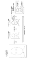
図3は、図1に示す撮像装置10におけるビューファインダ画像(ダウンコンバート画像)のエッジ情報表示(例えば、エッジ強調表示)の一例を示している。図3(a)は、本線出力となる4K解像度の画像信号による画像の一例を示している。図3(b)は、4K解像度の画像信号にダウンコンバート処理を施して得られたHD解像度の画像信号による画像の例を示している。図3(c)は、HD解像度の画像信号に、このHD解像度の画像信号に基づいて検出されたHD解像度のエッジ検出信号EG_1のみが付加された場合の画像の一例を示している。この場合、例えば、低周波数帯エッジが白色で強調表示される。
FIG. 3 shows an example of edge information display (for example, edge emphasis display) of the viewfinder image (down-converted image) in the
図3(d)は、HD解像度の画像信号に、HD解像度のエッジ検出信号EG_1とともに、4K解像度の撮像画像信号にフィルタリング処理を施し、さらにダウンコンバート処理を施して得られたHD解像度のエッジ検出信号EG_2が付加された場合の画像の一例を示している。この場合、例えば、低周波数帯エッジが白色で強調表示され、高周波数帯エッジは赤色で強調表示される。 FIG. 3D shows the HD resolution edge detection obtained by filtering the HD resolution image signal together with the HD resolution edge detection signal EG_1 and the 4K resolution captured image signal and further down-converting the signal. An example of an image when a signal EG_2 is added is shown. In this case, for example, the low frequency band edge is highlighted in white, and the high frequency band edge is highlighted in red.
このようなビューファインダ表示に基づいてフォーカスを合わせる際は、まず、例えば、白色に着色された低周波数帯エッジを見て大まかに合わせ、さらに、例えば、赤色に着色された高周波数帯エッジを指標に細かくフォーカスを合わせていく。これにより、HD解像度のビューファインダ表示のみで、4K解像度の画像に対してフォーカスを正確に合わせることが容易になる。 When focusing based on such viewfinder display, first, for example, look at the low frequency band edge colored white and roughly adjust it, and then, for example, index the high frequency band edge colored red Focus in detail. Accordingly, it becomes easy to accurately focus on the 4K resolution image only by the HD resolution viewfinder display.
[高周波数帯エッジ検出回路の構成例]
図4は、高周波数帯エッジ検出回路111の構成例を示している。この高周波数帯エッジ検出回路111に入力される4K解像度の撮像画像信号は、撮像部102、つまりベイヤー配列の色フィルタを持つ撮像素子を有する単板式のカラー撮像部で得られたものである。高周波数帯エッジ検出回路111は、この撮像画像信号に含まれる緑(G)の画素の信号に基づいて、HD解像度のエッジ検出信号EG_2を得る。
[Configuration example of high frequency band edge detection circuit]
FIG. 4 shows a configuration example of the high frequency band
ここで、ベイヤー配列の2*2の4画素(赤(R)1画素、緑(G)2画素、青(B)1画素)のセット(図2の太枠参照)に着目し、左下の緑(G)の画素をI0とし、右上の緑(G)の画素をI1とする。 Here, paying attention to the set of 2 * 2 4 pixels (red (R) 1 pixel, green (G) 2 pixel, blue (B) 1 pixel) of the Bayer array (see the thick frame in FIG. 2), Let the green (G) pixel be I0 and the upper right green (G) pixel be I1.
この高周波数帯エッジ検出回路111は、I0側エッジ検出部121-0と、I1側エッジ検出部121-1と、ダウンコンバート部122と、二乗化部123を有している。I0側エッジ検出部121-0は、ベイヤー配列の4画素セット毎に、近傍の4画素セットの画素I0,I1の信号(G信号)に基づき、画素I0に対応したエッジ検出信号を求める。また、I1側エッジ検出部121-1は、ベイヤー配列の4画素セット毎に、近傍の4画素セットの画素I0,I1の信号(G信号)に基づき、画素I1に対応したエッジ検出信号を求める。
The high frequency band
I0側エッジ検出部121-0は、I0側右上がり方向エッジ検出部124-R0と、I0側左上がり方向エッジ検出部124-L0と、セレクタ125-0を有している。I0側右上がり方向エッジ検出部124-R0は、ハイパスフィルタ131と、ローパスフィルタ132、コアリング部133、除算部134を有している。
The I0 side edge detection unit 121-0 includes an I0 side right upward direction edge detection unit 124-R0, an I0 side left upward direction edge detection unit 124-L0, and a selector 125-0. The I0 side right upward direction edge detection unit 124-R0 includes a high-
ハイパスフィルタ131は、I0側右上がり方向の高周波数帯の信号(エッジ検出信号)を検出する。本線出力の解像限界(ナイキスト周波数)を1としたとき、比率2:1でダウンコンバートされたファインダ出力の解像限界は0.5である。ハイパスフィルタ131で検出したい高周波数帯の信号(エッジ検出信号)は、ファインダ出力画像になく本線出力画像にのみ含まれる高周波数帯にある。
The high-
そのため、ハイパスフィルタ131の特性は、図5に示すように、周波数0.5以下の周波数帯では利得が0となり、0.5より上の周波数帯では利得が1となる特性を持つことが望ましい。周波数0.5以下の部分はファインダ出力画像のとる周波数帯であり、エッジ検出回路110にて検出可能であり、高周波数帯エッジ検出回路111で二重に検出する必要はない。また、周波数0.5以下のエッジにも反応するハイパスフィルタとしてしまうと、本線出力においてフォーカスがあっていない場合にもエッジが検出され、本線出力のフォーカスを正確に合わせる妨げとなる。
Therefore, as shown in FIG. 5, it is desirable that the high-
なお、このハイパスフィルタ131の特性を変える(フィルタ係数を変える)ことで,検出する周波数帯を変えることが可能である。例えば、被写体が動いた場合、エッジはより低周波数帯に落ちるが、その周波数帯にも反応するような(遮断周波数をより低くした)フィルタに変えることで、そのような場合にもエッジを検出するよう対応できる。 Note that the frequency band to be detected can be changed by changing the characteristics of the high-pass filter 131 (changing the filter coefficient). For example, if the subject moves, the edge falls to a lower frequency band, but the edge is detected by changing to a filter that responds to that frequency band (with a lower cutoff frequency). I can respond.
ベイヤー配列の色フィルタを持つ撮像素子を有する単板式のカラー撮像部の場合、本線出力画像と同等の解像度を持つのは緑(G)の画素の斜め方向の配列のみである。そのため、ハイパスフィルタ131は、ベイヤー配列の4画素セット毎に、画素I0を注目画素とし、右上がり方向に並ぶ所定数の画素I0,I1の信号(G信号)をタップ入力としてハイパスのフィルタリング処理を施し、高周波数帯の信号(エッジ検出信号)を検出する。
In the case of a single-plate color image pickup unit having an image pickup device having a Bayer color filter, only the green (G) pixel diagonal arrangement has the same resolution as the main line output image. For this reason, the high-
図6(a)は、タップ入力として使用される右上がり方向に並ぶ所定数の画素I0,I1の一例を示している。この例では、注目画素、その前の2画素、およびその後の2画素からなる5画素の信号(G信号)が使用されることを示している。そして、図6(b)に示すように、右上がり方向に並ぶ所定数の画素I0,I1から注目画素(画素I0)の右上がり方向のエッジ検出信号が得られる。 FIG. 6A shows an example of a predetermined number of pixels I0 and I1 arranged in the upward right direction used as tap input. In this example, it is shown that a signal (G signal) of 5 pixels including the target pixel, the previous two pixels, and the subsequent two pixels is used. Then, as shown in FIG. 6B, an edge detection signal in the upward direction of the target pixel (pixel I0) is obtained from a predetermined number of pixels I0 and I1 aligned in the upward direction.
ローパスフィルタ132は、ハイパスフィルタ131でベイヤー配列の4画素セット毎に注目画素(画素I0)の高周波数帯の信号(エッジ検出信号)が検出されるとき、この注目画素(画素I0)の近傍画素の信号レベルの平均値を求める。この場合、ローパスフィルタ132は、例えば、注目画素(画素I0)を含む右上がり方向に並ぶ所定数の画素I0,I1の信号(G信号)をタップ入力としてローパスのフィルタリング処理を施して、信号レベルの平均値を検出する。
When the high-
コアリング部133は、ハイパスフィルタ131で検出される高周波数帯の信号(エッジ検出信号)を入力とし、ノイズを抑圧して出力する。ハイパスフィルタ131は、エッジのみならず高周波数のランダムノイズにも反応してしまうため、ハイパスフィルタ131で検出される高周波数帯の信号(エッジ検出信号)には、高周波数のランダムノイズも含まれている。コアリング部133は、入力信号の振幅がある一定値より小さい場合にノイズ成分と見なして抑圧するものである。具体的には、入力信号のレベルをX、コアリングレベルをCORE_LEVELとすると、出力信号のレベルYは、以下の数式(1)で求められる。
The

撮像部102の撮像素子としてCMOS型の撮像素子を用いる場合、ノイズ量は信号レベルに依存する、つまり信号振幅が大きいほどノイズ振幅も増える、ことが知られている。そのため、コアリング部133は、図7に実線aで示すように、コアリングレベルを信号レベルに応じて増加させる。この場合、コアリング部133は、基準となる信号レベルとして、例えば、ローパスフィルタ132で得られる近傍画素の信号レベルの平均値を使用する。一方、撮像部102の撮像素子としてCCD型の撮像素子を用いる場合、ノイズ量は信号レベルに依存しないことが知られている。そのため、コアリング部133は、図7に破線bに示すように、信号レベルによらずにコアリングレベルを一定とする。
When a CMOS type image sensor is used as the image sensor of the
除算部134は、コアリング部133でノイズ抑圧処理された高周波数帯の信号(エッジ検出信号)を、ローパスフィルタ132で得られる近傍画素の信号レベルの平均値で除して正規化する。
The
自然画を撮像した場合、一般に、信号レベルが大きい(明るい)ほど空間的な変化量は大きく、信号レベルが小さい(暗い)ほど空間的な変化量は小さくなる。したがって、ハイパスフィルタ131の出力は、明るい領域では大きい値となりやすく、暗い領域では小さい値となりやすい。言いかえれば、明るい領域ではエッジを誤検出しやすく、暗い領域ではエッジが検出しにくいということになる。
When a natural image is captured, generally, the larger the signal level (brighter), the larger the spatial change amount, and the smaller the signal level (darker), the smaller the spatial change amount. Therefore, the output of the high-
除算部134は、これを改善するため、上述したような正規化処理を行う。この場合、ローパスフィルタ132の出力が大きい値となる明るい領域ではハイパスフィルタ131の出力の値は小さい値に、ローパスフィルタ132の出力が小さい値となる暗い領域ではハイパスフィルタ131の出力の値は大きい値に正規化される。したがって、除算部134は、正規化処理を行うことで、明るい領域ではエッジの誤検出を抑制し、暗い領域ではエッジを検出しやすくする。
The
I0側左上がり方向エッジ検出部124-L0は、I0側右上がり方向エッジ検出部124-R0と同様に構成され、I0側左上がり方向の高周波数帯の信号(エッジ検出信号)を検出する。このI0側左上がり方向エッジ検出部124-L0が有するハイパスフィルタは、ベイヤー配列の4画素セット毎に、画素I0を注目画素とし、左上がり方向に並ぶ所定数の画素I0,I1の信号(G信号)をタップ入力としてハイパスのフィルタリング処理を施し、高周波数帯の信号(エッジ検出信号)を検出する。 The I0 side left upward direction edge detection unit 124-L0 is configured in the same manner as the I0 side right upward direction edge detection unit 124-R0, and detects a high frequency band signal (edge detection signal) in the I0 side left upward direction. The high-pass filter of the I0 side left upward direction edge detection unit 124-L0 has a signal (G) of a predetermined number of pixels I0 and I1 aligned in the left upward direction with the pixel I0 as the target pixel for every four pixel sets in the Bayer array. Signal) is used as a tap input, and high-pass filtering is performed to detect a high-frequency band signal (edge detection signal).
図6(c)は、タップ入力として使用される左上がり方向に並ぶ所定数の画素I0,I1の一例を示している。この例では、注目画素、その前の2画素、およびその後の2画素からなる5画素の信号(G信号)が使用されることを示している。そして、図6(d)に示すように、左上がり方向に並ぶ所定数の画素I0,I1から注目画素(画素I0)の左上がり方向のエッジ検出信号が得られる。 FIG. 6C shows an example of a predetermined number of pixels I0 and I1 arranged in the upward left direction used as tap input. In this example, it is shown that a signal (G signal) of 5 pixels including the target pixel, the previous two pixels, and the subsequent two pixels is used. Then, as shown in FIG. 6D, an edge detection signal in the left upward direction of the target pixel (pixel I0) is obtained from a predetermined number of pixels I0 and I1 arranged in the left upward direction.
セレクタ125-0は、I0側右上がり方向エッジ検出部124-R0で検出される注目画素(画素I0)の右上がり方向のエッジ検出信号と、I0側左上がり方向エッジ検出部124-L0で検出される注目画素(画素I0)の左上がり方向のエッジ検出信号とから、絶対値の大きな信号を選択的に取り出し、I0側エッジ検出部121-0のエッジ検出信号、つまり画素I0に対応したエッジ検出信号として出力する。 The selector 125-0 detects the edge detection signal in the right upward direction of the target pixel (pixel I0) detected by the I0 side right upward direction edge detection unit 124-R0 and the I0 side left upward direction edge detection unit 124-L0. A signal having a large absolute value is selectively extracted from the edge detection signal in the upward left direction of the target pixel (pixel I0), and the edge detection signal of the I0 side edge detection unit 121-0, that is, the edge corresponding to the pixel I0 Output as a detection signal.
I1側エッジ検出部121-1は、I1側右上がり方向エッジ検出部124-R1と、I1側左上がり方向エッジ検出部124-L1と、セレクタ125-1を有している。I1側右上がり方向エッジ検出部124-R1は、I0側右上がり方向エッジ検出部124-R0と同様に構成され、I1側右上がり方向の高周波数帯の信号(エッジ検出信号)を検出する。このI1側右上がり方向エッジ検出部124-R1が有するハイパスフィルタは、ベイヤー配列の4画素セット毎に、画素I1を注目画素とし、右上がり方向に並ぶ所定数の画素I0,I1の信号(G信号)をタップ入力としてハイパスのフィルタリング処理を施し、高周波数帯の信号(エッジ検出信号)を検出する。 The I1 side edge detection unit 121-1 includes an I1 side right upward direction edge detection unit 124-R1, an I1 side left upward direction edge detection unit 124-L1, and a selector 125-1. The I1 side right upward direction edge detection unit 124-R1 is configured in the same manner as the I0 side right upward direction edge detection unit 124-R0, and detects a high-frequency band signal (edge detection signal) in the I1 side right upward direction. The high-pass filter of the I1 side upward rising edge detection unit 124-R1 uses a signal (G) of a predetermined number of pixels I0 and I1 aligned in the upward direction with the pixel I1 as the target pixel for every four pixel sets in the Bayer array. Signal) is used as a tap input, and high-pass filtering is performed to detect a high-frequency band signal (edge detection signal).
図8(a)は、タップ入力として使用される右上がり方向に並ぶ所定数の画素I0,I1の一例を示している。この例では、注目画素、その前の2画素、およびその後の2画素からなる5画素の信号(G信号)が使用されることを示している。そして、図8(b)に示すように、右上がり方向に並ぶ所定数の画素I0,I1から注目画素(画素I1)の右上がり方向のエッジ検出信号が得られる。 FIG. 8A shows an example of a predetermined number of pixels I0 and I1 arranged in the upward right direction used as tap input. In this example, it is shown that a signal (G signal) of 5 pixels including the target pixel, the previous two pixels, and the subsequent two pixels is used. Then, as shown in FIG. 8B, an edge detection signal in the upward direction of the target pixel (pixel I1) is obtained from a predetermined number of pixels I0 and I1 aligned in the upward direction.
I1側左上がり方向エッジ検出部124-L1は、I0側左上がり方向エッジ検出部124-L0と同様に構成され、I1側左上がり方向の高周波数帯の信号(エッジ検出信号)を検出する。このI1側左上がり方向エッジ検出部124-L1が有するハイパスフィルタは、ベイヤー配列の4画素セット毎に、画素I1を注目画素とし、左上がり方向に並ぶ所定数の画素I0,I1の信号(G信号)をタップ入力としてハイパスのフィルタリング処理を施し、高周波数帯の信号(エッジ検出信号)を検出する。 The I1 side left upward direction edge detection unit 124-L1 is configured in the same manner as the I0 side left upward direction edge detection unit 124-L0, and detects a signal (edge detection signal) in the high frequency band in the I1 side left upward direction. The high-pass filter of the I1 side left upward direction edge detection unit 124-L1 has a signal (G) of a predetermined number of pixels I0 and I1 aligned in the left upward direction with the pixel I1 as a target pixel for every four pixel sets in the Bayer array. Signal) is used as a tap input, and high-pass filtering is performed to detect a high-frequency band signal (edge detection signal).
図8(c)は、タップ入力として使用される左上がり方向に並ぶ所定数の画素I0,I1の一例を示している。この例では、注目画素、その前の2画素、およびその後の2画素からなる5画素の信号(G信号)が使用されることを示している。そして、図8(d)に示すように、左上がり方向に並ぶ所定数の画素I0,I1から注目画素(画素I1)の左上がり方向のエッジ検出信号が得られる。 FIG. 8C shows an example of a predetermined number of pixels I0 and I1 arranged in the upward left direction used as tap input. In this example, it is shown that a signal (G signal) of 5 pixels including the target pixel, the previous two pixels, and the subsequent two pixels is used. Then, as shown in FIG. 8D, an edge detection signal in the left upward direction of the target pixel (pixel I1) is obtained from a predetermined number of pixels I0 and I1 arranged in the left upward direction.
セレクタ125-1は、I1側右上がり方向エッジ検出部124-R1で検出される注目画素(画素I1)の右上がり方向のエッジ検出信号と、I1側左上がり方向エッジ検出部124-L1で検出される注目画素(画素I1)の左上がり方向のエッジ検出信号とから、絶対値の大きな信号を選択的に取り出し、I1側エッジ検出部121-1のエッジ検出信号、つまり画素I1に対応したエッジ検出信号として出力する。 The selector 125-1 detects an edge detection signal in the right upward direction of the target pixel (pixel I1) detected by the I1 side right upward direction edge detection unit 124-R1, and detects it by the I1 side left upward direction edge detection unit 124-L1. A signal having a large absolute value is selectively extracted from the edge detection signal in the upward left direction of the target pixel (pixel I1), and the edge detection signal of the I1 side edge detection unit 121-1, that is, the edge corresponding to the pixel I1 Output as a detection signal.
ダウンコンバート部122は、エッジ検出部121-0,121-1で検出された画素I0,I1に対応したエッジ検出信号にダウンコンバート処理を施して、HD解像度のエッジ検出信号を得る。
The down-
一般的に、ダウンコンバート処理は、「入力数−出力数」分の画素を何らかの方法で間引く処理である。例えば、単純に1画素おきに間引けば比率2:1のダウンコンバートを実現できる。しかし、例えば、図9(a)の入力に対して、単純間引きは、図9(b)に示すように行われ、間引かれる位相にあるエッジ情報は失われる(高周波数帯の信号が低域に折り返る)。 In general, the down-conversion process is a process of thinning out pixels corresponding to “number of inputs−number of outputs” by some method. For example, by simply thinning out every other pixel, down-conversion with a ratio of 2: 1 can be realized. However, for example, with respect to the input of FIG. 9A, simple thinning is performed as shown in FIG. 9B, and edge information in the thinned phase is lost (the signal in the high frequency band is low). Wrap around).
一般的に,ダウンコンバート処理では折り返し歪み(エイリアシング)を抑制するためにローパスフィルタ(LPF)による帯域制限を適用してから間引くことが行われる。しかし、例えば、図9(c)の入力に対して、帯域制限を適用してからの間引きは、図9(d)に示すように行われ、高周波数帯にあるエッジ情報はこの処理によって失われる。 In general, in down-conversion processing, in order to suppress aliasing (aliasing), thinning is performed after applying a band limitation by a low-pass filter (LPF). However, for example, thinning after applying the band limitation to the input in FIG. 9C is performed as shown in FIG. 9D, and edge information in the high frequency band is lost by this processing. Is called.
ダウンコンバート部122は、高解像度のエッジ成分の消失を伴わずにダウンコンバートを行う。ダウンコンバート部122は、4K解像度からHD解像度への2:1のダウンコンバート処理をする。ダウンコンバート部122は、ベイヤー配列の水平方向に並ぶ各4画素セットの画素I0,I1に対応したエッジ検出信号を一系列の信号として取り扱い、以下の処理を実行する。
The down-
すなわち、ダウンコンバート部122は、まず、上述の一系列の信号を、2*2画素の単位で分割する。次に、ダウンコンバート部122は、分割単位毎に、この分割単位の2*2画素分と続く分割単位の最初の1画素分の連続する2*2+1画素分のエッジ検出信号から2*2組の連続する2画素組を生成する。最後に、ダウンコンバート部122は、2*2組のうち差分絶対値が最大となる2画素の組を取り出す。
That is, the down-
図10(a1)は、ベイヤー配列の水平方向に並ぶ各4画素セットの画素I0,I1(「G」で示す)を示している。図10(a2)は、画素I0,I1に対応したエッジ検出信号を順に並べて一系列の信号とした場合のレベル変化を示している。 FIG. 10A1 shows pixels I0 and I1 (indicated by “G”) of each of the four pixel sets arranged in the horizontal direction of the Bayer array. FIG. 10A2 shows a level change when edge detection signals corresponding to the pixels I0 and I1 are sequentially arranged to form a series of signals.
図10(a3)は、一系列の信号が2*2画素の単位で分割され、分割単位毎に、この分割単位の2*2画素分と続く分割単位の最初の1画素分の連続する2*2+1画素分のエッジ検出信号から2*2組の連続する2画素組が生成されることを示している。例えば、「I0-1,I1-1,I0-2,I1-2」、[I0-3,I1-3,I0-4,I1-4]のそれぞれ4画素は分割単位を構成している。そして、「I0-1,I1-1,I0-2,I1-2」の分割単位に関しては、(I0-1,I1-1)、(I1-1,I0-2)、(I0-2,I1-2)、(I1-2,I0-3)の4組の2画素組が生成され、[I0-3,I1-3,I0-4,I1-4] の分割単位に関しては、(I0-3,I1-3)、(I1-3,I0-4)、(I0-4,I1-4)、(I1-4,I0-5)の4組の2画素組が生成される。 FIG. 10 (a3) shows that a series of signals is divided in units of 2 * 2 pixels, and for each division unit, 2 * 2 pixels corresponding to this division unit and the subsequent 2 pixels corresponding to the first one pixel of the subsequent division unit. * 2 * 2 sets of 2 consecutive pixel sets are generated from edge detection signals for 2 + 1 pixels. For example, each of “I0-1, I1-1, I0-2, I1-2” and [I0-3, I1-3, I0-4, I1-4] constitutes a division unit. For the division units of “I0-1, I1-1, I0-2, I1-2”, (I0-1, I1-1), (I1-1, I0-2), (I0-2, I1-2) and (I1-2, I0-3) are generated as two pixel groups, and the division unit of [I0-3, I1-3, I0-4, I1-4] is (I0 -3, I1-3), (I1-3, I0-4), (I0-4, I1-4), and (I1-4, I0-5), four sets of two pixels are generated.
図10(b1)は、ダウンコンバート後の水平方向に並ぶ画素(「G」で示す)を示している。図10(b2)は、ダウンコンバート後の各画素に対応したエッジ検出信号のレベル変化を示している。この場合、図10(b3)に示すように、「I0-1,I1-1,I0-2,I1-2」の分割単位に関しては差分絶対値が最も大きい(I1-2,I0-3)の2画素組が選択され、「I1-2」、「I0-3」の順に出力される。また、「I0-3,I1-3,I0-4,I1-4」の分割単位に関しては差分絶対値が最も大きい(I0-4,I1-4)の2画素組が選択され、「I0-4」、「I1-4」の順に出力される。 FIG. 10B1 illustrates pixels (indicated by “G”) arranged in the horizontal direction after down-conversion. FIG. 10B2 shows the level change of the edge detection signal corresponding to each pixel after down-conversion. In this case, as shown in FIG. 10 (b3), the difference absolute value is the largest for the division unit of “I0-1, I1-1, I0-2, I1-2” (I1-2, I0-3). Are selected and output in the order of “I1-2” and “I0-3”. For the division units of “I0-3, I1-3, I0-4, I1-4”, the two-pixel set having the largest difference absolute value (I0-4, I1-4) is selected, and “I0− Output in the order of “4” and “I1-4”.
上述のダウンコンバート処理では、2*2画素の入力に対して2画素の出力が得られるので、2:1のダウンコンバートを行っていることになる。また、このダウンコンバート処理では、変化量が最大となるエッジ検出信号をそのまま出力するため、ダウンコンバート後の信号に4K解像度のエッジがそのまま保存されている。 In the down-conversion process described above, since 2 pixel outputs are obtained for 2 * 2 pixel inputs, 2: 1 down-conversion is performed. In this down-conversion process, since the edge detection signal with the maximum amount of change is output as it is, 4K resolution edges are stored as they are in the down-converted signal.
図4に戻って、二乗化部123は、ダウンコンバート部122で生成されるHD解像度のエッジ検出信号を、乗算器123aを用いて二乗化して、出力する。この二乗化処理により、ハイパスフィルタ131による利得を二次関数的にすることができ、より狭い範囲の帯域の信号を強調できる。
Returning to FIG. 4, the squaring
図4に示す周波数帯エッジ検出回路111の動作を簡単に説明する。I0側右上がり方向エッジ検出部124-R0では、ベイヤー配列の4画素セット(図2の太枠参照)毎に、近傍の4画素セットの画素I0,I1の信号(G信号)に基づき、注目画素(画素I0)の右上がり方向のエッジ検出信号(高周波数帯の信号)が得られる(図6(a),(b)参照)。また、I0側左上がり方向エッジ検出部124-L0では、ベイヤー配列の4画素セット毎に、近傍の4画素セットの画素I0,I1の信号(G信号)に基づき、注目画素(画素I0)の左上がり方向のエッジ検出信号(高周波数帯の信号)が検出される(図6(c),(d)参照)。
The operation of the frequency band
I0側右上がり方向エッジ検出部124-R0で得られた画素I0の右上がり方向のエッジ検出信号は、セレクタ125-0に供給される。また、I0側左上がり方向エッジ検出部124-L0で検出された画素I0側の左上がり方向のエッジ検出信号は、セレクタ125-0に供給される。セレクタ125-0では、2つのエッジ検出信号から、絶対値の大きな信号が選択的に取り出され、I0側エッジ検出部121-0のエッジ検出信号、つまり画素I0に対応したエッジ検出信号として出力される(図6(e)参照)。 The edge detection signal in the right upward direction of the pixel I0 obtained by the I0 side right upward direction edge detection unit 124-R0 is supplied to the selector 125-0. Also, the edge detection signal in the left upward direction on the pixel I0 side detected by the I0 side left upward direction edge detection unit 124-L0 is supplied to the selector 125-0. The selector 125-0 selectively extracts a signal having a large absolute value from the two edge detection signals and outputs it as an edge detection signal of the I0 side edge detection unit 121-0, that is, an edge detection signal corresponding to the pixel I0. (See FIG. 6 (e)).
また、I1側右上がり方向エッジ検出部124-R1では、ベイヤー配列の4画素セット(図2の太枠参照)毎に、近傍の4画素セットの画素I0,I1の信号(G信号)に基づき、注目画素(画素I1)の右上がり方向のエッジ検出信号(高周波数帯の信号)が得られる(図8(a),(b)参照)。また、I1側左上がり方向エッジ検出部124-L1では、ベイヤー配列の4画素セット毎に、近傍の4画素セットの画素I0,I1の信号(G信号)に基づき、注目画素(画素I1)の左上がり方向のエッジ検出信号(高周波数帯の信号)が検出される(図8(c),(d)参照)。 Further, in the I1 side upward direction edge detection unit 124-R1, for each four-pixel set in the Bayer array (see the thick frame in FIG. 2), based on the signals (G signals) of the neighboring pixels I0 and I1 of the four-pixel set. Then, an edge detection signal (a signal in a high frequency band) in the upward direction of the target pixel (pixel I1) is obtained (see FIGS. 8A and 8B). Further, in the I1 side left upward edge detection unit 124-L1, for each four pixel set in the Bayer array, the pixel of interest (pixel I1) is determined based on the signals (G signals) of the pixels I0 and I1 in the neighboring four pixel sets. An edge detection signal (a signal in a high frequency band) in the upward left direction is detected (see FIGS. 8C and 8D).
I1側右上がり方向エッジ検出部124-R1で得られた画素I1の右上がり方向のエッジ検出信号は、セレクタ125-1に供給される。また、I1側左上がり方向エッジ検出部124-L1で検出された画素I1側の左上がり方向のエッジ検出信号は、セレクタ125-1に供給される。セレクタ125-1では、2つのエッジ検出信号から、絶対値の大きな信号が選択的に取り出され、I1側エッジ検出部121-1のエッジ検出信号、つまり画素I1に対応したエッジ検出信号として出力される(図8(e)参照)。 The edge detection signal in the right upward direction of the pixel I1 obtained by the I1 side upward right edge detection unit 124-R1 is supplied to the selector 125-1. The edge detection signal in the left upward direction on the pixel I1 side detected by the I1 side left upward direction edge detection unit 124-L1 is supplied to the selector 125-1. In the selector 125-1, a signal having a large absolute value is selectively extracted from the two edge detection signals and output as an edge detection signal of the I1 side edge detection unit 121-1, that is, an edge detection signal corresponding to the pixel I1. (See FIG. 8 (e)).
I0側エッジ検出部121-0から出力される画素I0に対応したエッジ検出信号およびI1側エッジ検出部121-1から出力される画素I1に対応したエッジ検出信号は、それぞれ、ダウンコンバート部122に供給される。ダウンコンバート部122では、画素I0,I1に対応したエッジ検出信号、つまり4K解像度のエッジ検出信号にダウンコンバート処理が施されて、HD解像度のエッジ検出信号が得られる。
The edge detection signal corresponding to the pixel I0 output from the I0 side edge detection unit 121-0 and the edge detection signal corresponding to the pixel I1 output from the I1 side edge detection unit 121-1 are respectively sent to the down-
この場合、高解像度のエッジ成分の消失を伴わずにダウンコンバートが行われる(図10参照)。例えば、まず、ベイヤー配列の水平方向に並ぶ各4画素セットの画素I0,I1に対応したエッジ検出信号が一系列の信号として取り扱われ、2*2画素の単位で分割される。そして、分割単位毎に、この分割単位の2*2画素分と続く分割単位の最初の1画素分の連続する2*2+1画素分のエッジ検出信号から2*2組の連続する2画素組が生成される。そして、2*2組のうち差分絶対値が最大となる2画素の組が取り出される。 In this case, down-conversion is performed without erasing the high-resolution edge component (see FIG. 10). For example, first, the edge detection signals corresponding to the pixels I0 and I1 of each of the four pixel sets arranged in the horizontal direction of the Bayer array are handled as a series of signals and divided in units of 2 * 2 pixels. For each division unit, 2 * 2 consecutive 2 pixel sets are obtained from the edge detection signals for 2 * 2 + 1 consecutive pixels for 2 * 2 pixels of the division unit and the first 1 pixel of the subsequent division unit. Generated. Then, a set of 2 pixels having the maximum difference absolute value is extracted from the 2 * 2 set.
ダウンコンバート部122で生成されたHD解像度のエッジ検出信号は、二乗化部123に供給されて二乗化された後、高周波数帯エッジ検出回路111の出力とされる。この高周波数帯エッジ検出回路111では、入力2画素「I0,I1」に対して出力1画素「O0」という割合でエッジ検出信号が得られる。つまり、4K解像度の撮像画像信号からHD解像度のエッジ検出信号EG_2が得られる。
The HD resolution edge detection signal generated by the down-
上述したように、図1に示す撮像装置10においては、ビューファインダ出力とされるHD解像度の画像信号に、エッジ検出回路110で得られた低周波数帯のエッジ検出信号EG_1と、高周波数帯エッジ検出回路111で得られた高周波数帯のエッジ検出信号EG_2が合成される。そのため、例えば、HD解像度のビューファインダに、HD解像度のエッジ情報を表示できるだけでなく、4K解像度のエッジ情報をも表示でき、したがって、HD解像度のビューファインダの表示を用いて、4K解像度カメラのフォーカスを正確に合わせることが可能となる。
As described above, in the
また、図1に示す撮像装置10においては、HD解像度の画像信号に、両周波数帯のエッジ検出信号EG_1,EG_2が合成されるものである。そして、その際に、両周波数帯のエッジ検出信号EG_1,EG_2によるエッジ情報表示(例えば、エッジ強調表示)が、例えば、色相、輝度、あるいは線種(実線、破線など)などの違いで区別可能に、合成される。
In the
そのため、例えば、両周波数帯のエッジ情報表示(エッジ強調表示)を同時に行うことが可能となり、ユーザのフォーカス合わせの容易性を高めることができる。例えば、ユーザは、HD解像度のエッジ情報表示を見てフォーカスを大まかに合わせ、さらに、4K解像度のエッジ状態表示を見て細かくフォーカスを合わせることが可能となる。この場合、2つのエッジ情報表示が区別可能とされることで、ユーザは、2つのエッジ情報表示の区別を容易に行うことができる。 Therefore, for example, edge information display (edge emphasis display) of both frequency bands can be performed at the same time, and the ease of focusing by the user can be improved. For example, the user can roughly focus by looking at the edge information display of HD resolution, and further finely focus by looking at the edge state display of 4K resolution. In this case, since the two edge information displays can be distinguished, the user can easily distinguish between the two edge information displays.
また、図1に示す撮像装置10においては、4K解像度の撮像画像信号にフィルタリング処理が施され、さらにダウンコンバート処理が施されてHD解像度のエッジ検出信号EG_2が生成されるものであり、ダウンコンバート処理では、変化量が最大となるエッジ検出信号をそのまま出力するものである。そのため、ダウンコンバート後の信号に4K解像度のエッジがそのまま保存され、HD解像度のビューファインダに4K解像度のエッジ情報表示を良好に行うことができる。
Further, in the
<2.変形例>
なお、上述実施の形態においては、撮像解像度が4K解像度であり、ビューファインダの表示解像度がHD解像度である場合の例を示した。そのため、高周波数帯エッジ検出回路111におけるダウンコンバート部122では、2:1の比率のダウンコンバートが行われている。例えば、撮像解像度とビューファインダの表示解像度の比率がN:1(Nは2以上の整数)である場合には、高周波数帯エッジ検出回路111では、N:1の比率のダウンコンバートが行われることになる。
<2. Modification>
In the above-described embodiment, an example in which the imaging resolution is 4K resolution and the viewfinder display resolution is HD resolution has been described. Therefore, the down-
この場合、ダウンコンバート部122は、ベイヤー配列の水平方向に並ぶ各4画素セットの画素I0,I1に対応したエッジ検出信号を一系列の信号として取り扱い、例えば、以下の処理を実行する。すなわち、ダウンコンバート部122は、まず、上述の一系列の信号を、2*N画素の単位で分割する。次に、ダウンコンバート部122は、分割単位毎に、この分割単位の2*N画素分と続く分割単位の最初の1画素分の連続する2*N+1画素分のエッジ検出信号から2*N組の連続する2画素組を生成する。最後に、ダウンコンバート部122は、2*N組のうち差分絶対値が最大となる2画素の組を取り出す。このダウンコンバート処理では、2*N画素の入力に対して2画素の出力が得られるので、N:1のダウンコンバートを行っていることになる。
In this case, the down-
また、例えば、撮像解像度とビューファインダの表示解像度の比率がN:M(NとMは互いに素)である場合も考えられる。ダウンコンバート部122は、ベイヤー配列の水平方向に並ぶ各4画素セットの画素I0,I1に対応したエッジ検出信号を一系列の信号として取り扱い、例えば、以下の処理を実行する。すなわち、ダウンコンバート部122は、まず、上述の一系列の信号を、N画素の単位で分割する。次に、ダウンコンバート部122は、分割単位毎に、この分割単位のN画素分と続く分割単位の最初からM−1画素分の連続するN+M−1画素分のエッジ検出信号からN組の連続するM画素組を生成する。最後に、ダウンコンバート部122は、N組のうち隣接差分絶対値和が最大となるM画素の組を取り出す。このダウンコンバート処理では、N画素の入力に対してM画素の出力が得られるので、N:Mのダウンコンバートを行っていることになる。
Further, for example, a case where the ratio between the imaging resolution and the viewfinder display resolution is N: M (N and M are relatively prime) may be considered. The down-
また、上述実施の形態においては、HD解像度のビューファインダに、HD解像度のエッジ情報表示と、4K解像度のエッジ情報表示の2段階の周波数帯のエッジ情報表示を同時に行う例を示した。しかし、3段階以上の周波数帯のエッジ情報表示を同時に行うことも考えられる。例えば、撮像解像度が8K解像度であり、ビューファインダの表示解像度がHD解像度である場合、上述実施の形態と同様の構成によって、HD解像度のエッジ情報表示と、4K解像度のエッジ情報表示と、さらに8K解像度のエッジ情報表示の3段階の周波数帯のエッジ情報表示を同時に行うことができる。 In the above-described embodiment, an example has been shown in which edge information display in two stages of HD resolution edge information display and 4K resolution edge information display is simultaneously performed on the HD resolution viewfinder. However, it is conceivable to simultaneously display edge information in three or more frequency bands. For example, when the imaging resolution is 8K resolution and the display resolution of the viewfinder is HD resolution, edge information display with HD resolution, edge information display with 4K resolution, and further 8K with the same configuration as the above embodiment. It is possible to simultaneously display edge information in the three frequency bands of resolution edge information display.
また、上述実施の形態においては、撮像部102が、ベイヤー配列の色フィルタを持つ撮像素子を有する単板式のカラー撮像部である例を示した。しかし、この撮像部102が、赤(R)、緑(G)、青(B)の3板式のカラー撮像部である例も考えられる。その場合にあっても、本技術を同様に適用できることは勿論である。
In the above-described embodiment, the example in which the
その場合、高周波数帯エッジ検出回路111では、例えば、画素毎に、水平方向、垂直方向の2方向のハイパスフィルタ処理でエッジ検出信号が得られて、絶対値のより大きい方がその画素のエッジ検出信号とされる。そして、この場合、高周波数帯エッジ検出回路111では、各画素のエッジ検出信号に対して、水平方向、垂直方向の2方向に、上述のN:1あるいはN:Mのダウンコンバート処理が施される。
In that case, in the high frequency band
また、本技術は、以下のような構成を取ることもできる。
(1)第1の解像度の画像信号にダウンコンバート処理を施して該第1の解像度より低い第2の解像度の画像信号を生成するダウンコンバート部と、
上記第1の解像度の画像信号に上記第2の解像度に対応した周波数より高い周波数帯の成分を抽出するフィルタリング処理を施し、該フィルタリング処理で得られたエッジ検出信号にダウンコンバート処理を施して上記第2の解像度のエッジ検出信号を得る高周波数帯エッジ検出部と、
上記ダウンコンバート部で生成された第2の解像度の画像信号に上記高周波数帯エッジ検出部で得られたエッジ検出信号を合成して表示用の第2の解像度の画像信号を得る合成部とを備える
画像信号処理装置。
(2)上記高周波数帯エッジ検出部におけるダウンコンバート処理は、
ダウンコンバート比率がN:1(Nは2以上の整数)であるとき、
上記フィルタリング処理で得られたエッジ検出信号を2N画素の単位で分割し、分割単位毎に、該分割単位の2N画素分と続く分割単位の最初の1画素分の連続する2N+1画素分のエッジ検出信号から2N組の連続する2画素の組を生成し、該2N組のうち差分絶対値が最大となる2画素の組を取り出す処理である
前記(1)に記載の画像信号処理装置。
(3)上記高周波数帯エッジ検出部は、
上記フィルタリング処理で得られるエッジ検出信号を上記第1の解像度の画像信号のレベル平均値で除して正規化し、該正規化されたエッジ検出信号に上記ダウンコンバート処理を施す
前記(1)または(2)に記載の画像信号処理装置。
(4)上記ダウンコンバート部で生成される第2の解像度の画像信号に基づいて上記第2の解像度のエッジ検出信号を得る低周波帯エッジ検出部をさらに備え、
上記合成部は、
上記ダウンコンバート部で生成された第2の解像度の画像信号に、上記高周波数帯エッジ検出部で得られたエッジ検出信号である第1のエッジ検出信号と共に、上記低周波数帯エッジ検出部で得られたエッジ検出信号である第2のエッジ検出信号を合成して、上記表示用の第2の解像度の画像信号を得る
前記(1)から(3)のいずれかに記載の画像信号処理装置。
(5)上記合成部は、
上記第1のエッジ検出信号によるエッジ情報表示と上記第2のエッジ検出信号によるエッジ情報表示が区別可能に、上記第1の解像度の画像信号に、上記第1のエッジ検出信号および上記第2のエッジ検出信号を合成する
前記(4)に記載の画像信号処理装置。
(6)上記第1のエッジ検出信号および上記第2のエッジ検出信号によるエッジ情報表示の区別は、色相、輝度あるいは線種の違いにより行われる
前記(5)に記載の画像信号処理装置。
(7)上記第1の解像度の画像信号はベイヤー配列の色フィルタを持つ撮像素子を有する単板式のカラー撮像部の出力画像信号であり、
上記高周波数帯エッジ検出部は、斜め方向に配列される緑の画素の信号に基づいて上記第2の解像度のエッジ検出信号を得る
前記(1)から(6)のいずれかに記載の画像信号処理装置。
(8)上記第1の解像度は4K解像度であり、上記第2の解像度はHD解像度である
前記(1)から(7)のいずれかに記載の画像信号処理装置。
(9)第1の解像度の画像信号にダウンコンバート処理を施して該第1の解像度より低い第2の解像度の画像信号を生成するステップと、
上記第1の解像度の画像信号に上記第2の解像度に対応した周波数より高い周波数帯の成分を抽出するフィルタリング処理を施し、該フィルタリング処理で得られたエッジ検出信号にダウンコンバート処理を施して上記第2の解像度のエッジ検出信号を得るステップと、
上記生成された第2の解像度の画像信号に上記得られたエッジ検出信号を合成して表示用の第2の解像度の画像信号を得るステップとを備える
画像信号処理方法。
(10)第1の解像度の画像信号を得る撮像部と、
上記撮像部で得られた第1の解像度の画像信号を処理してビューファインダ表示用の、上記第1の解像度より低い第2の解像度の画像信号を得る画像信号処理部とを備え、
上記画像信号処理部は、
上記第1の解像度の画像信号にダウンコンバート処理を施して該第1の解像度より低い第2の解像度の画像信号を生成するダウンコンバート部と、
上記第1の解像度の画像信号に上記第2の解像度に対応した周波数より高い周波数帯の成分を抽出するフィルタリング処理を施し、該フィルタリング処理で得られたエッジ検出信号にダウンコンバート処理を施して上記第2の解像度のエッジ検出信号を得る高周波数帯エッジ検出部と、
上記ダウンコンバート部で生成された第2の解像度の画像信号に上記高周波数帯エッジ検出部で得られたエッジ検出信号を合成して上記表示用の第2の解像度の画像信号を得る合成部とを有する
撮像装置。
(11)上記画像信号処理部は、
上記ダウンコンバート部で生成された第2の解像度の画像信号に基づいて上記第2の解像度のエッジ検出信号を得る低周波数帯エッジ検出部をさらに備え、
上記合成部は、
上記ダウンコンバート部で生成された第2の解像度の画像信号に、上記高周波数帯エッジ検出部で得られたエッジ検出信号である第1のエッジ検出信号と共に、上記低周波数帯エッジ検出部で得られたエッジ検出信号である第2のエッジ検出信号を合成して、上記表示用の第2の解像度の画像信号を得る
前記(10)に記載の撮像装置。
(12)上記合成部は、
上記第1のエッジ検出信号によるエッジ情報表示と上記第2のエッジ検出信号によるエッジ情報表示が区別可能に、上記第2の解像度の画像信号に、上記第1のエッジ検出信号および上記第2のエッジ検出信号を合成する
前記(11)に記載の撮像装置。
(13)上記第1の解像度は4K解像度であり、上記第2の解像度はHD解像度である
前記(10)から(12)のいずれかに記載の撮像装置。
(14)表示素子に、
撮像画像信号に基づく画像に重ねて、
上記撮像画像信号の所定周波数以下の周波数帯の成分に基づいて検出されたエッジ検出信号による第1のエッジ情報表示と、上記撮像画像信号の上記所定周波数より高い周波数帯の成分に基づいて検出されたエッジ検出信号による第2のエッジ情報表示とを、区別可能に行う
画像表示方法。
(15)上記第1のエッジ情報表示および上記第2のエッジ情報表示の区別は、色相、輝度あるいは線種の違いにより行われる
前記(14)に記載の画像表示方法。
(16)上記所定周波数は、上記表示素子の解像度に対応する周波数である
前記(14)または(15)に記載の画像表示方法。
(17)上記撮像画像信号は4K解像度の撮像部の出力画像信号であり、上記表示素子はHD解像度の表示素子である
前記(14)から(16)のいずれかに記載の画像表示方法。
Moreover, this technique can also take the following structures.
(1) a down-conversion unit that performs down-conversion processing on an image signal having a first resolution to generate an image signal having a second resolution lower than the first resolution;
Filtering processing for extracting a component in a frequency band higher than the frequency corresponding to the second resolution is performed on the image signal of the first resolution, down-conversion processing is performed on the edge detection signal obtained by the filtering processing, and A high frequency band edge detection unit for obtaining an edge detection signal of the second resolution;
A synthesis unit for synthesizing the edge detection signal obtained by the high-frequency band edge detection unit with the second resolution image signal generated by the down-conversion unit to obtain a second resolution image signal for display; An image signal processing apparatus.
(2) The down-conversion process in the high frequency band edge detection unit is as follows:
When the down-conversion ratio is N: 1 (N is an integer of 2 or more)
The edge detection signal obtained by the filtering process is divided in units of 2N pixels, and for each division unit, edge detection is performed for 2N + 1 pixels in succession for 2N pixels in the division unit and the first one pixel in the subsequent division unit. 2. The image signal processing device according to (1), which is a process of generating 2N sets of two consecutive pixels from a signal and taking out a set of two pixels having the maximum difference absolute value from the 2N sets.
(3) The high frequency band edge detector
The edge detection signal obtained by the filtering process is normalized by dividing by the level average value of the image signal of the first resolution, and the down-conversion process is performed on the normalized edge detection signal (1) or ( The image signal processing apparatus according to 2).
(4) a low frequency band edge detection unit that obtains the edge detection signal of the second resolution based on the image signal of the second resolution generated by the down-conversion unit;
The synthesis unit is
The image signal of the second resolution generated by the down-conversion unit is obtained by the low frequency band edge detection unit together with the first edge detection signal which is the edge detection signal obtained by the high frequency band edge detection unit. The image signal processing device according to any one of (1) to (3), wherein the second edge detection signal that is the received edge detection signal is synthesized to obtain an image signal having the second resolution for display.
(5) The synthesis unit is
The edge information display by the first edge detection signal and the edge information display by the second edge detection signal can be distinguished, and the first edge detection signal and the second edge image are displayed in the first resolution image signal. The image signal processing device according to (4), wherein the edge detection signal is combined.
(6) The image signal processing apparatus according to (5), wherein the edge information display is distinguished based on a hue, luminance, or line type based on the first edge detection signal and the second edge detection signal.
(7) The image signal of the first resolution is an output image signal of a single-plate type color imaging unit having an imaging element having a Bayer color filter.
The image signal according to any one of (1) to (6), wherein the high frequency band edge detection unit obtains an edge detection signal of the second resolution based on a signal of green pixels arranged in an oblique direction. Processing equipment.
(8) The image signal processing device according to any one of (1) to (7), wherein the first resolution is 4K resolution and the second resolution is HD resolution.
(9) performing a down-conversion process on the first resolution image signal to generate a second resolution image signal lower than the first resolution;
Filtering processing for extracting a component in a frequency band higher than the frequency corresponding to the second resolution is performed on the image signal of the first resolution, down-conversion processing is performed on the edge detection signal obtained by the filtering processing, and Obtaining an edge detection signal of a second resolution;
An image signal processing method comprising: synthesizing the obtained edge detection signal with the generated second resolution image signal to obtain a second resolution image signal for display.
(10) an imaging unit that obtains an image signal having a first resolution;
An image signal processing unit for processing a first resolution image signal obtained by the imaging unit to obtain a second resolution image signal lower than the first resolution for viewfinder display;
The image signal processor is
A down-conversion unit for performing a down-conversion process on the first resolution image signal to generate a second resolution image signal lower than the first resolution;
Filtering processing for extracting a component in a frequency band higher than the frequency corresponding to the second resolution is performed on the image signal of the first resolution, down-conversion processing is performed on the edge detection signal obtained by the filtering processing, and A high frequency band edge detection unit for obtaining an edge detection signal of the second resolution;
A synthesis unit for synthesizing the edge detection signal obtained by the high frequency band edge detection unit with the image signal of the second resolution generated by the down-conversion unit to obtain the image signal of the second resolution for display; An imaging apparatus.
(11) The image signal processing unit
A low frequency band edge detection unit that obtains an edge detection signal of the second resolution based on the image signal of the second resolution generated by the down-conversion unit;
The synthesis unit is
The image signal of the second resolution generated by the down-conversion unit is obtained by the low frequency band edge detection unit together with the first edge detection signal which is the edge detection signal obtained by the high frequency band edge detection unit. The imaging device according to (10), wherein the second edge detection signal, which is the obtained edge detection signal, is synthesized to obtain the second resolution image signal for display.
(12) The synthesis unit
The edge information display by the first edge detection signal and the edge information display by the second edge detection signal can be distinguished, and the first edge detection signal and the second edge image are displayed in the second resolution image signal. The imaging device according to (11), wherein edge detection signals are combined.
(13) The imaging device according to any one of (10) to (12), wherein the first resolution is 4K resolution, and the second resolution is HD resolution.
(14) In the display element,
Overlaid on the image based on the captured image signal,
First edge information display by an edge detection signal detected based on a frequency band component equal to or lower than a predetermined frequency of the captured image signal, and detected based on a frequency band component higher than the predetermined frequency of the captured image signal. An image display method in which the second edge information display by the edge detection signal is distinguishable.
(15) The image display method according to (14), wherein the distinction between the first edge information display and the second edge information display is performed based on a difference in hue, luminance, or line type.
(16) The image display method according to (14) or (15), wherein the predetermined frequency is a frequency corresponding to a resolution of the display element.
(17) The image display method according to any one of (14) to (16), wherein the captured image signal is an output image signal of an imaging unit having a 4K resolution, and the display element is an HD resolution display element.
10・・・撮像装置
101・・・レンズ
102・・・撮像部
103・・・撮像系補正回路
104・・・ゲイン調整回路
105・・・色分離回路
106・・・ニー・ガンマ補正回路
107・・・出力信号生成回路(本線出力)
108・・・ダウンコンバート回路
109・・・出力信号生成回路(ファインダ出力)
110・・・エッジ検出回路
111・・・高周波数帯エッジ検出回路
121-0・・・I0側エッジ検出部
121-1・・・I1側エッジ検出部
122・・・ダウンコンバート部
123・・・二乗化回路
123a・・・乗算器
124-R0・・・I0側右上がり方向エッジ検出部
124-L0・・・I0側左上がり方向エッジ検出部
124-R1・・・I1側右上がり方向エッジ検出部
124-L1・・・I1側左上がり方向エッジ検出部
125-0,125-1・・・セレクタ
131・・・ハイパスフィルタ
132・・・ローパスフィルタ
133・・・コアリング部
134・・・除算部
DESCRIPTION OF
108 ... down-
DESCRIPTION OF
Claims (17)
上記第1の解像度の画像信号に上記第2の解像度に対応した周波数より高い周波数帯の成分を抽出するフィルタリング処理を施し、該フィルタリング処理で得られたエッジ検出信号にダウンコンバート処理を施して上記第2の解像度のエッジ検出信号を得る高周波数帯エッジ検出部と、
上記ダウンコンバート部で生成された第2の解像度の画像信号に上記高周波数帯エッジ検出部で得られたエッジ検出信号を合成して表示用の第2の解像度の画像信号を得る合成部とを備える
画像信号処理装置。 A down-conversion unit that performs down-conversion processing on the first resolution image signal to generate a second resolution image signal lower than the first resolution;
Filtering processing for extracting a component in a frequency band higher than the frequency corresponding to the second resolution is performed on the image signal of the first resolution, down-conversion processing is performed on the edge detection signal obtained by the filtering processing, and A high frequency band edge detection unit for obtaining an edge detection signal of the second resolution;
A synthesis unit for synthesizing the edge detection signal obtained by the high-frequency band edge detection unit with the second resolution image signal generated by the down-conversion unit to obtain a second resolution image signal for display; An image signal processing apparatus.
ダウンコンバート比率がN:1(Nは2以上の整数)であるとき、
上記フィルタリング処理で得られたエッジ検出信号を2N画素の単位で分割し、分割単位毎に、該分割単位の2N画素分と続く分割単位の最初の1画素分の連続する2N+1画素分のエッジ検出信号から2N組の連続する2画素の組を生成し、該2N組のうち差分絶対値が最大となる2画素の組を取り出す処理である
請求項1に記載の画像信号処理装置。 The down-conversion process in the high frequency band edge detection unit is as follows.
When the down-conversion ratio is N: 1 (N is an integer of 2 or more)
The edge detection signal obtained by the filtering process is divided in units of 2N pixels, and for each division unit, edge detection is performed for 2N + 1 pixels in succession for 2N pixels in the division unit and the first one pixel in the subsequent division unit. The image signal processing apparatus according to claim 1, wherein the image signal processing apparatus is a process of generating 2N sets of 2 consecutive pixels from a signal and taking out a set of 2 pixels having the maximum difference absolute value from the 2N sets.
上記フィルタリング処理で得られるエッジ検出信号を上記第1の解像度の画像信号のレベル平均値で除して正規化し、該正規化されたエッジ検出信号に上記ダウンコンバート処理を施す
請求項1に記載の画像信号処理装置。 The high frequency band edge detector is
The edge detection signal obtained by the filtering process is normalized by dividing by an average level value of the image signal of the first resolution, and the down-conversion process is performed on the normalized edge detection signal. Image signal processing device.
上記合成部は、
上記ダウンコンバート部で生成された第2の解像度の画像信号に、上記高周波数帯エッジ検出部で得られたエッジ検出信号である第1のエッジ検出信号と共に、上記低周波数帯エッジ検出部で得られたエッジ検出信号である第2のエッジ検出信号を合成して、上記表示用の第2の解像度の画像信号を得る
請求項1に記載の画像信号処理装置。 A low frequency band edge detection unit that obtains the edge detection signal of the second resolution based on the image signal of the second resolution generated by the down-conversion unit;
The synthesis unit is
The image signal of the second resolution generated by the down-conversion unit is obtained by the low frequency band edge detection unit together with the first edge detection signal which is the edge detection signal obtained by the high frequency band edge detection unit. The image signal processing apparatus according to claim 1, wherein the second edge detection signal that is the detected edge detection signal is synthesized to obtain the image signal having the second resolution for display.
上記第1のエッジ検出信号によるエッジ情報表示と上記第2のエッジ検出信号によるエッジ情報表示が区別可能に、上記第1の解像度の画像信号に、上記第1のエッジ検出信号および上記第2のエッジ検出信号を合成する
請求項4に記載の画像信号処理装置。 The synthesis unit is
The edge information display by the first edge detection signal and the edge information display by the second edge detection signal can be distinguished, and the first edge detection signal and the second edge image are displayed in the first resolution image signal. The image signal processing apparatus according to claim 4, wherein the edge detection signals are combined.
請求項5に記載の画像信号処理装置。 The image signal processing apparatus according to claim 5, wherein the distinction of the edge information display based on the first edge detection signal and the second edge detection signal is performed based on a difference in hue, luminance, or line type.
上記高周波数帯エッジ検出部は、斜め方向に配列される緑の画素の信号に基づいて上記第2の解像度のエッジ検出信号を得る
請求項1に記載の画像信号処理装置。 The image signal of the first resolution is an output image signal of a single plate type color imaging unit having an imaging element having a color filter with a Bayer array,
The image signal processing device according to claim 1, wherein the high frequency band edge detection unit obtains an edge detection signal having the second resolution based on signals of green pixels arranged in an oblique direction.
請求項1に記載の画像信号処理装置。 The image signal processing apparatus according to claim 1, wherein the first resolution is 4K resolution, and the second resolution is HD resolution.
上記第1の解像度の画像信号に上記第2の解像度に対応した周波数より高い周波数帯の成分を抽出するフィルタリング処理を施し、該フィルタリング処理で得られたエッジ検出信号にダウンコンバート処理を施して上記第2の解像度のエッジ検出信号を得るステップと、
上記生成された第2の解像度の画像信号に上記得られたエッジ検出信号を合成して表示用の第2の解像度の画像信号を得るステップとを備える
画像信号処理方法。 Performing a down-conversion process on the first resolution image signal to generate a second resolution image signal lower than the first resolution;
Filtering processing for extracting a component in a frequency band higher than the frequency corresponding to the second resolution is performed on the image signal of the first resolution, down-conversion processing is performed on the edge detection signal obtained by the filtering processing, and Obtaining an edge detection signal of a second resolution;
An image signal processing method comprising: synthesizing the obtained edge detection signal with the generated second resolution image signal to obtain a second resolution image signal for display.
上記撮像部で得られた第1の解像度の画像信号を処理してビューファインダ表示用の、上記第1の解像度より低い第2の解像度の画像信号を得る画像信号処理部とを備え、
上記画像信号処理部は、
上記第1の解像度の画像信号にダウンコンバート処理を施して該第1の解像度より低い第2の解像度の画像信号を生成するダウンコンバート部と、
上記第1の解像度の画像信号に上記第2の解像度に対応した周波数より高い周波数帯の成分を抽出するフィルタリング処理を施し、該フィルタリング処理で得られたエッジ検出信号にダウンコンバート処理を施して上記第2の解像度のエッジ検出信号を得る高周波数帯エッジ検出部と、
上記ダウンコンバート部で生成された第2の解像度の画像信号に上記高周波数帯エッジ検出部で得られたエッジ検出信号を合成して上記表示用の第2の解像度の画像信号を得る合成部とを有する
撮像装置。 An imaging unit for obtaining an image signal of a first resolution;
An image signal processing unit for processing a first resolution image signal obtained by the imaging unit to obtain a second resolution image signal lower than the first resolution for viewfinder display;
The image signal processor is
A down-conversion unit for performing a down-conversion process on the first resolution image signal to generate a second resolution image signal lower than the first resolution;
Filtering processing for extracting a component in a frequency band higher than the frequency corresponding to the second resolution is performed on the image signal of the first resolution, down-conversion processing is performed on the edge detection signal obtained by the filtering processing, and A high frequency band edge detection unit for obtaining an edge detection signal of the second resolution;
A synthesis unit for synthesizing the edge detection signal obtained by the high frequency band edge detection unit with the image signal of the second resolution generated by the down-conversion unit to obtain the image signal of the second resolution for display; An imaging apparatus.
上記ダウンコンバート部で生成された第2の解像度の画像信号に基づいて上記第2の解像度のエッジ検出信号を得る低周波数帯エッジ検出部をさらに備え、
上記合成部は、
上記ダウンコンバート部で生成された第2の解像度の画像信号に、上記高周波数帯エッジ検出部で得られたエッジ検出信号である第1のエッジ検出信号と共に、上記低周波数帯エッジ検出部で得られたエッジ検出信号である第2のエッジ検出信号を合成して、上記表示用の第2の解像度の画像信号を得る
請求項10に記載の撮像装置。 The image signal processor is
A low frequency band edge detection unit that obtains an edge detection signal of the second resolution based on the image signal of the second resolution generated by the down-conversion unit;
The synthesis unit is
The image signal of the second resolution generated by the down-conversion unit is obtained by the low frequency band edge detection unit together with the first edge detection signal which is the edge detection signal obtained by the high frequency band edge detection unit. The imaging device according to claim 10, wherein the second edge detection signal that is the obtained edge detection signal is synthesized to obtain an image signal having the second resolution for display.
上記第1のエッジ検出信号によるエッジ情報表示と上記第2のエッジ検出信号によるエッジ情報表示が区別可能に、上記第2の解像度の画像信号に、上記第1のエッジ検出信号および上記第2のエッジ検出信号を合成する
請求項11に記載の撮像装置。 The synthesis unit is
The edge information display by the first edge detection signal and the edge information display by the second edge detection signal can be distinguished, and the first edge detection signal and the second edge image are displayed in the second resolution image signal. The imaging device according to claim 11, wherein the edge detection signals are combined.
請求項10に記載の撮像装置。 The imaging device according to claim 10, wherein the first resolution is 4K resolution, and the second resolution is HD resolution.
撮像画像信号に基づく画像に重ねて、
上記撮像画像信号の所定周波数以下の周波数帯の成分に基づいて検出されたエッジ検出信号による第1のエッジ情報表示と、上記撮像画像信号の上記所定周波数より高い周波数帯の成分に基づいて検出されたエッジ検出信号による第2のエッジ情報表示とを、区別可能に行う
画像表示方法。 In the display element,
Overlaid on the image based on the captured image signal,
First edge information display by an edge detection signal detected based on a frequency band component equal to or lower than a predetermined frequency of the captured image signal, and detected based on a frequency band component higher than the predetermined frequency of the captured image signal. An image display method in which the second edge information display by the edge detection signal is distinguishable.
請求項14に記載の画像表示方法。 The image display method according to claim 14, wherein the distinction between the first edge information display and the second edge information display is performed based on a difference in hue, luminance, or line type.
請求項14に記載の画像表示方法。 The image display method according to claim 14, wherein the predetermined frequency is a frequency corresponding to a resolution of the display element.
請求項14に記載の画像表示方法。 The image display method according to claim 14, wherein the captured image signal is an output image signal of an imaging unit having a 4K resolution, and the display element is an HD resolution display element.
Priority Applications (5)
| Application Number | Priority Date | Filing Date | Title |
|---|---|---|---|
| JP2013109399A JP2014230176A (en) | 2013-05-23 | 2013-05-23 | Image signal processing apparatus, image signal processing method, imaging apparatus, and image display method |
| US14/254,186 US9467646B2 (en) | 2013-05-23 | 2014-04-16 | Apparatus and method for processing image signal, imaging apparatus, and method for displaying image |
| CN201410207000.9A CN104184929B (en) | 2013-05-23 | 2014-05-16 | Handle device and method, imaging device and the method for showing image of picture signal |
| US15/260,727 US9924133B2 (en) | 2013-05-23 | 2016-09-09 | Apparatus and method for processing image signal, imaging apparatus, and method for displaying image |
| US15/901,248 US10819947B2 (en) | 2013-05-23 | 2018-02-21 | Apparatus and method for processing image signal, imaging apparatus, and method for displaying image |
Applications Claiming Priority (1)
| Application Number | Priority Date | Filing Date | Title |
|---|---|---|---|
| JP2013109399A JP2014230176A (en) | 2013-05-23 | 2013-05-23 | Image signal processing apparatus, image signal processing method, imaging apparatus, and image display method |
Publications (1)
| Publication Number | Publication Date |
|---|---|
| JP2014230176A true JP2014230176A (en) | 2014-12-08 |
Family
ID=51935172
Family Applications (1)
| Application Number | Title | Priority Date | Filing Date |
|---|---|---|---|
| JP2013109399A Pending JP2014230176A (en) | 2013-05-23 | 2013-05-23 | Image signal processing apparatus, image signal processing method, imaging apparatus, and image display method |
Country Status (3)
| Country | Link |
|---|---|
| US (3) | US9467646B2 (en) |
| JP (1) | JP2014230176A (en) |
| CN (1) | CN104184929B (en) |
Cited By (3)
| Publication number | Priority date | Publication date | Assignee | Title |
|---|---|---|---|---|
| WO2018168571A1 (en) * | 2017-03-15 | 2018-09-20 | ソニー株式会社 | Imaging device, video signal processing device, and video signal processing method |
| WO2020084999A1 (en) * | 2018-10-25 | 2020-04-30 | ソニー株式会社 | Image processing device, image processing method, and program |
| US10944948B2 (en) | 2015-04-08 | 2021-03-09 | Sony Corporation | Imaging apparatus, imaging system, and imaging method |
Families Citing this family (13)
| Publication number | Priority date | Publication date | Assignee | Title |
|---|---|---|---|---|
| JP2014230176A (en) | 2013-05-23 | 2014-12-08 | ソニー株式会社 | Image signal processing apparatus, image signal processing method, imaging apparatus, and image display method |
| JP6299227B2 (en) * | 2014-01-16 | 2018-03-28 | ソニー株式会社 | Camera device |
| CN104038699B (en) * | 2014-06-27 | 2016-04-06 | 努比亚技术有限公司 | The reminding method of focusing state and filming apparatus |
| WO2016084608A1 (en) * | 2014-11-25 | 2016-06-02 | ソニー株式会社 | Endoscope system, method for operating endoscope system, and program |
| WO2016163324A1 (en) * | 2015-04-07 | 2016-10-13 | ソニー株式会社 | Image signal processing apparatus, image signal processing method, and image capture apparatus |
| CN105262953B (en) * | 2015-10-30 | 2018-11-16 | 努比亚技术有限公司 | A kind of mobile terminal and its method of control shooting |
| CA3024995A1 (en) | 2016-05-24 | 2017-11-30 | Morphotrust Usa, Llc | Document image quality assessment |
| CN114073067A (en) * | 2019-07-17 | 2022-02-18 | 索尼集团公司 | Image processing apparatus, imaging apparatus, image processing method, and program |
| JP7232160B2 (en) * | 2019-09-19 | 2023-03-02 | Tvs Regza株式会社 | IMAGE QUALITY CIRCUIT, VIDEO PROCESSING DEVICE, AND SIGNAL FEATURE DETECTION METHOD |
| US20220159318A1 (en) * | 2019-10-28 | 2022-05-19 | Radius Co., Ltd. | Streaming data generating device, streaming data delivery system, and method of generating streaming data |
| WO2022072279A1 (en) | 2020-09-30 | 2022-04-07 | United States Postal Service | System and method for extracting a region of interest from a captured image of a mailpiece or parcel label |
| US11755858B2 (en) * | 2020-12-04 | 2023-09-12 | United States Postal Service | System and method for extracting a computer readable code from a captured image of a distribution item |
| CN114257695B (en) * | 2021-12-14 | 2023-11-07 | 成都信和创业科技有限责任公司 | Universal imaging definition detection method for image projection equipment |
Family Cites Families (12)
| Publication number | Priority date | Publication date | Assignee | Title |
|---|---|---|---|---|
| JPS6110360A (en) * | 1984-06-26 | 1986-01-17 | Canon Inc | Picture processing device |
| DE60122993T2 (en) * | 2000-10-19 | 2007-10-18 | Sanyo Electric Co., Ltd., Moriguchi | Image data output device and receiving device |
| US20040051793A1 (en) * | 2002-09-18 | 2004-03-18 | Tecu Kirk S. | Imaging device |
| JP4458925B2 (en) * | 2004-05-14 | 2010-04-28 | キヤノン株式会社 | Video processing device |
| JP4561273B2 (en) * | 2004-09-22 | 2010-10-13 | ソニー株式会社 | Image processing apparatus and method, and program |
| JP4325599B2 (en) * | 2005-08-25 | 2009-09-02 | ソニー株式会社 | Imaging apparatus and display control method |
| US8155184B2 (en) * | 2008-01-16 | 2012-04-10 | Sony Corporation | Video coding system using texture analysis and synthesis in a scalable coding framework |
| CN101770759B (en) * | 2008-12-17 | 2014-04-02 | 香港应用科技研究院有限公司 | Method and device for downsampling based on sub-pixel |
| GB2500417B8 (en) * | 2012-03-21 | 2017-06-07 | Sony Computer Entertainment Europe Ltd | Camera device, system and method of imaging |
| JP2014021928A (en) * | 2012-07-23 | 2014-02-03 | Canon Inc | Image processor, image processing method and program |
| JP2014230176A (en) * | 2013-05-23 | 2014-12-08 | ソニー株式会社 | Image signal processing apparatus, image signal processing method, imaging apparatus, and image display method |
| JP6305194B2 (en) * | 2014-05-08 | 2018-04-04 | キヤノン株式会社 | Image processing apparatus, imaging apparatus, and image processing method |
-
2013
- 2013-05-23 JP JP2013109399A patent/JP2014230176A/en active Pending
-
2014
- 2014-04-16 US US14/254,186 patent/US9467646B2/en active Active
- 2014-05-16 CN CN201410207000.9A patent/CN104184929B/en active Active
-
2016
- 2016-09-09 US US15/260,727 patent/US9924133B2/en active Active
-
2018
- 2018-02-21 US US15/901,248 patent/US10819947B2/en active Active
Cited By (9)
| Publication number | Priority date | Publication date | Assignee | Title |
|---|---|---|---|---|
| US10944948B2 (en) | 2015-04-08 | 2021-03-09 | Sony Corporation | Imaging apparatus, imaging system, and imaging method |
| WO2018168571A1 (en) * | 2017-03-15 | 2018-09-20 | ソニー株式会社 | Imaging device, video signal processing device, and video signal processing method |
| EP3598732A4 (en) * | 2017-03-15 | 2020-03-11 | Sony Corporation | Imaging device, video signal processing device, and video signal processing method |
| JPWO2018168571A1 (en) * | 2017-03-15 | 2020-05-14 | ソニー株式会社 | Imaging device, video signal processing device, and video signal processing method |
| US10778889B2 (en) | 2017-03-15 | 2020-09-15 | Sony Corporation | Image pickup apparatus, video signal processing apparatus, and video signal processing method |
| JP7063321B2 (en) | 2017-03-15 | 2022-05-09 | ソニーグループ株式会社 | Imaging device, video signal processing device and video signal processing method |
| WO2020084999A1 (en) * | 2018-10-25 | 2020-04-30 | ソニー株式会社 | Image processing device, image processing method, and program |
| US11676242B2 (en) | 2018-10-25 | 2023-06-13 | Sony Group Corporation | Image processing apparatus and image processing method |
| JP7456385B2 (en) | 2018-10-25 | 2024-03-27 | ソニーグループ株式会社 | Image processing device, image processing method, and program |
Also Published As
| Publication number | Publication date |
|---|---|
| US10819947B2 (en) | 2020-10-27 |
| US9924133B2 (en) | 2018-03-20 |
| US20140347557A1 (en) | 2014-11-27 |
| US20180249118A1 (en) | 2018-08-30 |
| CN104184929A (en) | 2014-12-03 |
| US9467646B2 (en) | 2016-10-11 |
| US20170006256A1 (en) | 2017-01-05 |
| CN104184929B (en) | 2019-05-10 |
Similar Documents
| Publication | Publication Date | Title |
|---|---|---|
| JP2014230176A (en) | Image signal processing apparatus, image signal processing method, imaging apparatus, and image display method | |
| US9420175B2 (en) | Image processing system, image processing method, and computer-readable medium | |
| US8363123B2 (en) | Image pickup apparatus, color noise reduction method, and color noise reduction program | |
| JP4284570B2 (en) | Imaging apparatus and method thereof | |
| JP5451782B2 (en) | Image processing apparatus and image processing method | |
| JP5694293B2 (en) | System and method for selectively combining video frame image data | |
| WO2016047240A1 (en) | Image processing device, image pickup element, image pickup device, and image processing method | |
| JP2012239103A (en) | Image processing device, image processing method, and program | |
| JP2010088105A (en) | Imaging apparatus and method, and program | |
| US10778881B2 (en) | Video signal processing device, video signal processing method, and camera device | |
| US8520099B2 (en) | Imaging apparatus, integrated circuit, and image processing method | |
| WO2016163324A1 (en) | Image signal processing apparatus, image signal processing method, and image capture apparatus | |
| US10979620B2 (en) | Image processing apparatus for providing information for focus adjustment, control method of the same, and storage medium | |
| JP6305194B2 (en) | Image processing apparatus, imaging apparatus, and image processing method | |
| EP2645702B1 (en) | Image capturing apparatus, control method therefor, and program | |
| JP5748513B2 (en) | Imaging device | |
| JP5900273B2 (en) | Focus evaluation value generation device, focus evaluation value generation method, and focus evaluation value generation program | |
| JP2011082726A (en) | Image reproducing apparatus, and imaging apparatus | |
| JP6408884B2 (en) | Image processing apparatus, image processing method, and program | |
| JP5014277B2 (en) | Focus auxiliary signal processing device | |
| WO2017122553A1 (en) | Image processing device, image processing method and image capturing device | |
| JP7038935B2 (en) | Image processing device, image processing method, and image processing program | |
| WO2015079481A1 (en) | Image capture method and image capture apparatus | |
| Lim et al. | 30.4: Trilateral Filter for Depth Map Interpolation in 3D Video | |
| JP2010252293A (en) | Image processing apparatus and imaging apparatus |