JP2014182203A - Display device, and electronic equipment - Google Patents
Display device, and electronic equipment Download PDFInfo
- Publication number
- JP2014182203A JP2014182203A JP2013055243A JP2013055243A JP2014182203A JP 2014182203 A JP2014182203 A JP 2014182203A JP 2013055243 A JP2013055243 A JP 2013055243A JP 2013055243 A JP2013055243 A JP 2013055243A JP 2014182203 A JP2014182203 A JP 2014182203A
- Authority
- JP
- Japan
- Prior art keywords
- signal
- potential
- transfer circuit
- display device
- shift
- Prior art date
- Legal status (The legal status is an assumption and is not a legal conclusion. Google has not performed a legal analysis and makes no representation as to the accuracy of the status listed.)
- Pending
Links
Images


Classifications
-
- G—PHYSICS
- G06—COMPUTING; CALCULATING OR COUNTING
- G06F—ELECTRIC DIGITAL DATA PROCESSING
- G06F3/00—Input arrangements for transferring data to be processed into a form capable of being handled by the computer; Output arrangements for transferring data from processing unit to output unit, e.g. interface arrangements
- G06F3/01—Input arrangements or combined input and output arrangements for interaction between user and computer
- G06F3/03—Arrangements for converting the position or the displacement of a member into a coded form
- G06F3/041—Digitisers, e.g. for touch screens or touch pads, characterised by the transducing means
- G06F3/0416—Control or interface arrangements specially adapted for digitisers
- G06F3/04166—Details of scanning methods, e.g. sampling time, grouping of sub areas or time sharing with display driving
-
- G—PHYSICS
- G02—OPTICS
- G02F—OPTICAL DEVICES OR ARRANGEMENTS FOR THE CONTROL OF LIGHT BY MODIFICATION OF THE OPTICAL PROPERTIES OF THE MEDIA OF THE ELEMENTS INVOLVED THEREIN; NON-LINEAR OPTICS; FREQUENCY-CHANGING OF LIGHT; OPTICAL LOGIC ELEMENTS; OPTICAL ANALOGUE/DIGITAL CONVERTERS
- G02F1/00—Devices or arrangements for the control of the intensity, colour, phase, polarisation or direction of light arriving from an independent light source, e.g. switching, gating or modulating; Non-linear optics
- G02F1/01—Devices or arrangements for the control of the intensity, colour, phase, polarisation or direction of light arriving from an independent light source, e.g. switching, gating or modulating; Non-linear optics for the control of the intensity, phase, polarisation or colour
- G02F1/13—Devices or arrangements for the control of the intensity, colour, phase, polarisation or direction of light arriving from an independent light source, e.g. switching, gating or modulating; Non-linear optics for the control of the intensity, phase, polarisation or colour based on liquid crystals, e.g. single liquid crystal display cells
- G02F1/133—Constructional arrangements; Operation of liquid crystal cells; Circuit arrangements
- G02F1/1333—Constructional arrangements; Manufacturing methods
- G02F1/13338—Input devices, e.g. touch panels
-
- G—PHYSICS
- G06—COMPUTING; CALCULATING OR COUNTING
- G06F—ELECTRIC DIGITAL DATA PROCESSING
- G06F3/00—Input arrangements for transferring data to be processed into a form capable of being handled by the computer; Output arrangements for transferring data from processing unit to output unit, e.g. interface arrangements
- G06F3/01—Input arrangements or combined input and output arrangements for interaction between user and computer
- G06F3/03—Arrangements for converting the position or the displacement of a member into a coded form
- G06F3/041—Digitisers, e.g. for touch screens or touch pads, characterised by the transducing means
- G06F3/0412—Digitisers structurally integrated in a display
-
- G—PHYSICS
- G06—COMPUTING; CALCULATING OR COUNTING
- G06F—ELECTRIC DIGITAL DATA PROCESSING
- G06F3/00—Input arrangements for transferring data to be processed into a form capable of being handled by the computer; Output arrangements for transferring data from processing unit to output unit, e.g. interface arrangements
- G06F3/01—Input arrangements or combined input and output arrangements for interaction between user and computer
- G06F3/03—Arrangements for converting the position or the displacement of a member into a coded form
- G06F3/041—Digitisers, e.g. for touch screens or touch pads, characterised by the transducing means
- G06F3/0416—Control or interface arrangements specially adapted for digitisers
- G06F3/0418—Control or interface arrangements specially adapted for digitisers for error correction or compensation, e.g. based on parallax, calibration or alignment
- G06F3/04184—Synchronisation with the driving of the display or the backlighting unit to avoid interferences generated internally
-
- G—PHYSICS
- G06—COMPUTING; CALCULATING OR COUNTING
- G06F—ELECTRIC DIGITAL DATA PROCESSING
- G06F3/00—Input arrangements for transferring data to be processed into a form capable of being handled by the computer; Output arrangements for transferring data from processing unit to output unit, e.g. interface arrangements
- G06F3/01—Input arrangements or combined input and output arrangements for interaction between user and computer
- G06F3/03—Arrangements for converting the position or the displacement of a member into a coded form
- G06F3/041—Digitisers, e.g. for touch screens or touch pads, characterised by the transducing means
- G06F3/044—Digitisers, e.g. for touch screens or touch pads, characterised by the transducing means by capacitive means
- G06F3/0445—Digitisers, e.g. for touch screens or touch pads, characterised by the transducing means by capacitive means using two or more layers of sensing electrodes, e.g. using two layers of electrodes separated by a dielectric layer
-
- G—PHYSICS
- G06—COMPUTING; CALCULATING OR COUNTING
- G06F—ELECTRIC DIGITAL DATA PROCESSING
- G06F3/00—Input arrangements for transferring data to be processed into a form capable of being handled by the computer; Output arrangements for transferring data from processing unit to output unit, e.g. interface arrangements
- G06F3/01—Input arrangements or combined input and output arrangements for interaction between user and computer
- G06F3/03—Arrangements for converting the position or the displacement of a member into a coded form
- G06F3/041—Digitisers, e.g. for touch screens or touch pads, characterised by the transducing means
- G06F3/044—Digitisers, e.g. for touch screens or touch pads, characterised by the transducing means by capacitive means
- G06F3/0446—Digitisers, e.g. for touch screens or touch pads, characterised by the transducing means by capacitive means using a grid-like structure of electrodes in at least two directions, e.g. using row and column electrodes
-
- G—PHYSICS
- G09—EDUCATION; CRYPTOGRAPHY; DISPLAY; ADVERTISING; SEALS
- G09G—ARRANGEMENTS OR CIRCUITS FOR CONTROL OF INDICATING DEVICES USING STATIC MEANS TO PRESENT VARIABLE INFORMATION
- G09G3/00—Control arrangements or circuits, of interest only in connection with visual indicators other than cathode-ray tubes
- G09G3/20—Control arrangements or circuits, of interest only in connection with visual indicators other than cathode-ray tubes for presentation of an assembly of a number of characters, e.g. a page, by composing the assembly by combination of individual elements arranged in a matrix no fixed position being assigned to or needed to be assigned to the individual characters or partial characters
- G09G3/2092—Details of a display terminals using a flat panel, the details relating to the control arrangement of the display terminal and to the interfaces thereto
-
- G—PHYSICS
- G11—INFORMATION STORAGE
- G11C—STATIC STORES
- G11C19/00—Digital stores in which the information is moved stepwise, e.g. shift registers
- G11C19/18—Digital stores in which the information is moved stepwise, e.g. shift registers using capacitors as main elements of the stages
- G11C19/182—Digital stores in which the information is moved stepwise, e.g. shift registers using capacitors as main elements of the stages in combination with semiconductor elements, e.g. bipolar transistors, diodes
- G11C19/184—Digital stores in which the information is moved stepwise, e.g. shift registers using capacitors as main elements of the stages in combination with semiconductor elements, e.g. bipolar transistors, diodes with field-effect transistors, e.g. MOS-FET
-
- G—PHYSICS
- G09—EDUCATION; CRYPTOGRAPHY; DISPLAY; ADVERTISING; SEALS
- G09G—ARRANGEMENTS OR CIRCUITS FOR CONTROL OF INDICATING DEVICES USING STATIC MEANS TO PRESENT VARIABLE INFORMATION
- G09G2310/00—Command of the display device
- G09G2310/02—Addressing, scanning or driving the display screen or processing steps related thereto
- G09G2310/0264—Details of driving circuits
- G09G2310/0286—Details of a shift registers arranged for use in a driving circuit
-
- G—PHYSICS
- G09—EDUCATION; CRYPTOGRAPHY; DISPLAY; ADVERTISING; SEALS
- G09G—ARRANGEMENTS OR CIRCUITS FOR CONTROL OF INDICATING DEVICES USING STATIC MEANS TO PRESENT VARIABLE INFORMATION
- G09G2310/00—Command of the display device
- G09G2310/02—Addressing, scanning or driving the display screen or processing steps related thereto
- G09G2310/0264—Details of driving circuits
- G09G2310/0291—Details of output amplifiers or buffers arranged for use in a driving circuit
Landscapes
- Engineering & Computer Science (AREA)
- Theoretical Computer Science (AREA)
- General Engineering & Computer Science (AREA)
- Physics & Mathematics (AREA)
- General Physics & Mathematics (AREA)
- Human Computer Interaction (AREA)
- Nonlinear Science (AREA)
- Microelectronics & Electronic Packaging (AREA)
- Computer Hardware Design (AREA)
- Crystallography & Structural Chemistry (AREA)
- Chemical & Material Sciences (AREA)
- Optics & Photonics (AREA)
- Mathematical Physics (AREA)
- Power Engineering (AREA)
- Control Of Indicators Other Than Cathode Ray Tubes (AREA)
- Liquid Crystal Display Device Control (AREA)
- Liquid Crystal (AREA)
- Position Input By Displaying (AREA)
Abstract
Description
本開示は、画像を表示する表示装置、およびそのような表示装置を備えた電子機器に関する。 The present disclosure relates to a display device that displays an image and an electronic apparatus including such a display device.
近年、表示装置は、画質や消費電力などの観点から、液晶表示装置、プラズマ表示装置、有機EL表示装置などの様々な種類のものが開発されており、それらの特性に応じて、据置型の表示装置の他、携帯電話、携帯型情報端末など、様々な電子機器に適用されている。 In recent years, various types of display devices such as liquid crystal display devices, plasma display devices, and organic EL display devices have been developed from the viewpoint of image quality and power consumption. In addition to display devices, it is applied to various electronic devices such as mobile phones and portable information terminals.
表示装置は、一般に、線順次走査を行うことにより画像を表示する(例えば、特許文献1および特許文献2)。具体的には、例えば液晶表示装置では、まず、走査線信号駆動回路(ゲートドライバ)が、マトリックス状に配置された画素のうちの1行(1水平ライン)を表示駆動の対象として選択する。そして、信号線駆動回路(ソースドライバ)が、その選択された画素に対して画素信号を供給する。これにより、選択された1水平ラインに係る画素に画素信号が書き込まれる。表示装置は、このような画素信号の書き込み動作を、表示面全面にわたり順次走査しつつ行うことにより、画像を表示するようになっている。
Generally, a display device displays an image by performing line sequential scanning (for example,
ところで、表示装置では、表示面全面にわたって線順次走査する際、中断および再開を繰り返すことにより間欠的に線順次走査を行う場合がある。このような場合でも、画質の低下を抑えることが望まれる。 By the way, in the display device, when line-sequential scanning is performed over the entire display surface, line-sequential scanning may be intermittently performed by repeating interruption and resumption. Even in such a case, it is desired to suppress a decrease in image quality.
本開示は、間欠的に線順次走査を行う場合に、画質の低下を抑えることができる表示装置および電子機器を提供することを目的とする。 An object of the present disclosure is to provide a display device and an electronic apparatus that can suppress degradation in image quality when intermittent line-sequential scanning is performed.
本開示の表示装置は、走査信号が印加される複数の走査信号線を有する表示部と、入力されたシフト信号を一時的に保持し、中断期間を有するクロック信号に同期して、該シフト信号を次段へ順次伝達するシフト動作を行う複数段の転送回路を有し、前記シフト信号を保持する転送回路に対応する走査信号線へ前記走査信号を出力するシフトレジスタと、前記クロック信号の前記中断期間に、前記シフト信号を保持する転送回路に該シフト信号の電位を保持するための電位保持信号を伝達する信号線と、を備える。 A display device according to the present disclosure includes a display unit having a plurality of scanning signal lines to which a scanning signal is applied, a shift signal that is temporarily input, and the shift signal in synchronization with a clock signal having an interruption period. And a shift register that outputs a scanning signal to a scanning signal line corresponding to the transfer circuit that holds the shift signal, and And a signal line for transmitting a potential holding signal for holding the potential of the shift signal to the transfer circuit holding the shift signal in the interruption period.
本開示の電子機器は、前述した表示装置と、前記表示装置に入力信号を供給する制御装置とを有する。 An electronic apparatus according to the present disclosure includes the display device described above and a control device that supplies an input signal to the display device.
本開示の表示装置および電子機器は、クロック信号の中断期間に、電位保持信号線を介して電位保持信号を転送回路に与え、転送回路に設定されている電位を保つことを実現できる。その結果、表示装置および電子機器は、間欠的に線順次走査を行う場合に、画質の低下を抑えることができる。 The display device and the electronic apparatus according to the present disclosure can realize that the potential holding signal is supplied to the transfer circuit through the potential holding signal line and the potential set in the transfer circuit is maintained during the interruption period of the clock signal. As a result, the display device and the electronic device can suppress deterioration in image quality when intermittent line-sequential scanning is performed.
本開示によれば、間欠的に線順次走査を行う場合に、画質の低下を抑えることができる表示装置および電子機器を提供することができる。 According to the present disclosure, it is possible to provide a display device and an electronic apparatus that can suppress deterioration in image quality when intermittent line sequential scanning is performed.
以下、本開示の実施の形態について、図面を参照して詳細に説明する。なお、説明は以下の順序で行う。
1.静電容量式タッチ検出の基本原理
2.実施の形態
3.適用例
Hereinafter, embodiments of the present disclosure will be described in detail with reference to the drawings. The description will be given in the following order.
1. 1. Basic principle of capacitive
<1.静電容量式タッチ検出の基本原理>
まず最初に、図1〜図3を参照して、表示装置におけるタッチ検出の基本原理について説明する。このタッチ検出方式は、静電容量式のタッチセンサとして具現化されるものであり、例えば図1(A)に示したように、誘電体Dを挟んで互いに対向配置された一対の電極(駆動電極E1およびタッチ検出電極E2)を用い、容量素子を構成する。この構造は、図1(B)に示した等価回路として表される。駆動電極E1、タッチ検出電極E2および誘電体Dによって、容量素子C1が構成される。容量素子C1は、その一端が交流信号源(駆動信号源)Sに接続され、他端Pは抵抗器Rを介して接地されると共に、電圧検出器(タッチ検出回路)DETに接続される。交流信号源Sから駆動電極E1(容量素子C1の一端)に所定の周波数(例えば数kHz〜数十kHz程度)の交流矩形波Sg(図3(B))を印加すると、タッチ検出電極E2(容量素子C1の他端P)に、図3(A)に示したような出力波形(タッチ検出信号Vdet)が現れる。なお、この交流矩形波Sgは、後述する交流駆動信号VcomACに相当するものである。
<1. Basic Principle of Capacitive Touch Detection>
First, the basic principle of touch detection in a display device will be described with reference to FIGS. This touch detection method is embodied as a capacitive touch sensor. For example, as shown in FIG. 1A, a pair of electrodes (drives) arranged opposite to each other with a dielectric D interposed therebetween. A capacitive element is configured using the electrode E1 and the touch detection electrode E2). This structure is expressed as an equivalent circuit shown in FIG. The drive element E1, the touch detection electrode E2, and the dielectric D constitute a capacitive element C1. One end of the capacitive element C1 is connected to an AC signal source (drive signal source) S, and the other end P is grounded via a resistor R and also connected to a voltage detector (touch detection circuit) DET. When an AC rectangular wave Sg (FIG. 3B) having a predetermined frequency (for example, about several kHz to several tens kHz) is applied from the AC signal source S to the drive electrode E1 (one end of the capacitive element C1), the touch detection electrode E2 ( An output waveform (touch detection signal Vdet) as shown in FIG. 3A appears at the other end P) of the capacitive element C1. The AC rectangular wave Sg corresponds to an AC drive signal VcomAC described later.
指が接触(または近接)していない状態では、図1に示したように、容量素子C1に対する充放電に伴って、容量素子C1の容量値に応じた電流I0が流れる。このときの容量素子C1の他端Pの電位波形は、例えば図3(A)の波形V0のようになり、これが電圧検出器DETによって検出される。 In a state where the finger is not in contact (or close proximity), as shown in FIG. 1, a current I0 corresponding to the capacitance value of the capacitive element C1 flows along with charging / discharging of the capacitive element C1. The potential waveform at the other end P of the capacitive element C1 at this time is, for example, a waveform V0 in FIG. 3A, which is detected by the voltage detector DET.
一方、指が接触(または近接)した状態では、図2(A)、(B)に示したように、指によって形成される容量素子C2が容量素子C1に直列に追加された形となる。この状態では、容量素子C1、C2に対する充放電に伴って、それぞれ電流I1、I2が流れる。このときの容量素子C1の他端Pの電位波形は、例えば図3(A)の波形V1のようになり、これが電圧検出器DETによって検出される。このとき、他端Pの電位は、容量素子C1、C2を流れる電流I1、I2の値によって定まる分圧電位となる。このため、波形V1は、非接触状態での波形V0よりも小さい値となる。電圧検出器DETは、検出した電圧を所定のしきい値電圧Vthと比較し、このしきい値電圧Vth以上であれば非接触状態と判断する一方、しきい値電圧Vth未満であれば接触状態と判断する。このようにして、タッチ検出が可能となる。 On the other hand, when the finger is in contact (or close), as shown in FIGS. 2A and 2B, the capacitor C2 formed by the finger is added in series to the capacitor C1. In this state, currents I1 and I2 flow in accordance with charging and discharging of the capacitive elements C1 and C2, respectively. The potential waveform at the other end P of the capacitive element C1 at this time is, for example, a waveform V1 in FIG. 3A, and this is detected by the voltage detector DET. At this time, the potential at the other end P is a divided potential determined by the values of the currents I1 and I2 flowing through the capacitive elements C1 and C2. For this reason, the waveform V1 is smaller than the waveform V0 in the non-contact state. The voltage detector DET compares the detected voltage with a predetermined threshold voltage Vth, and if it is equal to or higher than this threshold voltage Vth, it is judged as a non-contact state, while if it is lower than the threshold voltage Vth, it is in a contact state Judge. In this way, touch detection is possible.
<2.実施の形態>
[構成例]
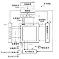
(全体構成例)
図4は、本開示の実施の形態に係る表示装置1の一構成例を表すものである。この表示装置1は、液晶表示パネルと静電容量式のタッチパネルとを一体化した、いわゆるインセルタイプの表示装置である。
<2. Embodiment>
[Configuration example]
(Overall configuration example)
FIG. 4 illustrates a configuration example of the
この表示装置1は、制御部11と、ゲートドライバ12と、ソースドライバ13と、駆動電極ドライバ14と、タッチセンサ付き表示部15と、タッチ検出部18とを備えている。
The
制御部11は、制御装置2から供給される映像信号Vdispに基づいて、ゲートドライバ12、ソースドライバ13、駆動電極ドライバ14、およびタッチ検出部18に対してそれぞれ制御信号を供給し、これらがお互いに同期して動作するように制御する回路である。
Based on the video signal Vdisp supplied from the
ゲートドライバ12は、制御部11から供給される制御信号に基づいて、タッチセンサ付き表示部15の表示駆動の対象となる1水平ラインを順次選択する、走査線信号駆動回路としての機能を有している。具体的には、ゲートドライバ12は、後述するように、走査信号VGをタッチセンサ付き表示部15に供給することにより、タッチセンサ付き表示部15の液晶表示部16(後述)にマトリックス状に形成されている画素Pixのうちの1行(1水平ライン)を表示駆動の対象として順次選択するようになっている。
The
ソースドライバ13は、制御部11から供給される制御信号に基づいて、液晶表示部16の各画素Pix(後述)に画素信号Vsigを供給する回路である。具体的には、ソースドライバ13は、後述するように、画素信号Vsigを、表示駆動の対象として選択された1水平ラインを構成する各画素Pixにそれぞれ供給するものである。
The
駆動電極ドライバ14は、制御部11から供給される制御信号に基づいて、タッチセンサ付き表示部15の駆動電極COML(後述)に駆動信号Vcomを供給する回路である。具体的には、駆動電極ドライバ14は、後述するように、タッチ検出駆動の対象となる駆動電極COMLに対して、交流駆動信号VcomAC(後述)を時分割的に順次印加すると共に、それ以外の駆動電極COMLに対して、直流駆動信号VcomDC(後述)を印加するようになっている。
The drive electrode driver 14 is a circuit that supplies a drive signal Vcom to drive electrodes COML (described later) of the
タッチセンサ付き表示部15は、タッチセンサを内蔵した表示部であり、液晶表示部16と、タッチセンサ部17とを有する。液晶表示部16は、ゲートドライバ12から供給される走査信号VGに従って、1水平ラインずつ順次走査して表示を行うものである。タッチセンサ部17は、上述した静電容量式タッチ検出の基本原理に基づいて動作するものであり、駆動電極ドライバ14から供給される交流駆動信号VcomACに応じてタッチ検出信号Vdetを出力することにより、順次走査してタッチ検出を行うようになっている。
The
タッチ検出部18は、制御部11から供給される制御信号と、タッチセンサ部17から供給されたタッチ検出信号Vdetに基づいて、外部近接物体を検出するものである。
The
この構成により、表示装置1は、映像信号Vdispに基づいて表示動作を行いつつ、タッチ検出動作を行う。その際、表示装置1は、後述するように、線順次走査を行うことにより表示動作を行うと共に、表示動作を中断している期間においてタッチ検出動作を行うようになっている。
With this configuration, the
(タッチセンサ付き表示部15)
次に、タッチセンサ付き表示部15の構成例を詳細に説明する。
(
Next, a configuration example of the
図5は、タッチセンサ付き表示部15の要部断面構造の例を表すものである。このタッチセンサ付き表示部15は、画素基板20と、この画素基板20に対向して配置された対向基板30と、画素基板20と対向基板30との間に挿設された液晶層9とを備えている。
FIG. 5 illustrates an example of a cross-sectional structure of a main part of the
画素基板20は、回路基板としてのTFT基板21と、駆動電極COMLと、画素電極22とを有している。TFT基板21は、各種電極や配線(後述する画素信号線SGLや走査信号線GCL等)、薄膜トランジスタ(TFT;Thin Film Transistor)などが形成される回路基板として機能するものである。TFT基板21は例えばガラスにより構成されるものである。TFT基板21の上には、駆動電極COMLが形成される。駆動電極COMLは、複数の画素Pix(後述)に共通の電圧を供給するための電極である。この駆動電極COMLは、液晶表示動作のための共通駆動電極として機能すると共に、タッチ検出動作のための駆動電極としても機能するものである。駆動電極COMLの上には絶縁層23が形成され、その上に画素電極22が形成される。画素電極22は、表示を行うための画素信号を供給するための電極であり、透光性を有するものである。駆動電極COMLおよび画素電極22は、例えばITO(Indium Tin Oxide)により構成される。
The
対向基板30は、ガラス基板31と、カラーフィルタ32と、タッチ検出電極TDLとを有している。カラーフィルタ32は、ガラス基板31の一方の面に形成されている。このカラーフィルタ32は、例えば赤(R)、緑(G)、青(B)の3色のカラーフィルタ層を周期的に配列して構成したもので、各表示画素にR、G、Bの3色が1組として対応付けられている。また、ガラス基板31の他方の面には、タッチ検出電極TDLが形成されている。タッチ検出電極TDLは、例えばITOにより構成され、透光性を有する電極である。このタッチ検出電極TDLの上には、偏光板35が配設されている。
The
液晶層9は、表示機能層として機能するものであり、電界の状態に応じて通過する光を変調するものである。この電界は、駆動電極COMLの電圧と画素電極22の電圧との電位差により形成される。液晶層9には、FFS(フリンジフィールドスイッチング)やIPS(インプレーンスイッチング)等の横電界モードの液晶が用いられる。
The
なお、液晶層9と画素基板20との間、および液晶層9と対向基板30との間には、それぞれ配向膜が配設され、また、画素基板20の下面側には入射側偏光板が配置されるが、ここでは図示を省略している。
An alignment film is provided between the
図6は、液晶表示部16における画素構造の構成例を表すものである。液晶表示部16は、マトリックス状に配列した複数の画素Pixを有している。各画素Pixは、3つのサブ画素SPixにより構成される。この3つのサブ画素SPixは、図5に示したカラーフィルタ32の3色(RGB)にそれぞれ対応するように配置されている。サブ画素SPixは、TFT素子Trおよび液晶素子LCを有している。TFT素子Trは、薄膜トランジスタにより構成されるものであり、この例では、nチャネルのMOS(Metal Oxide Semiconductor)型のTFTで構成されている。TFT素子Trのソースは画素信号線SGLに接続され、ゲートは走査信号線GCLに接続され、ドレインは液晶素子LCの一端に接続されている。液晶素子LCは、一端がTFT素子Trのドレインに接続され、他端が駆動電極COMLに接続されている。
FIG. 6 illustrates a configuration example of a pixel structure in the liquid
サブ画素SPixは、走査信号線GCLにより、液晶表示部16の同じ行に属する他のサブ画素SPixと互いに接続されている。走査信号線GCLは、ゲートドライバ12と接続され、ゲートドライバ12より走査信号VGが供給される。また、サブ画素SPixは、画素信号線SGLにより、液晶表示部16の同じ列に属する他のサブ画素SPixと互いに接続されている。画素信号線SGLは、ソースドライバ13と接続され、ソースドライバ13より画素信号Vsigが供給される。
The sub-pixel SPix is connected to another sub-pixel SPix belonging to the same row of the liquid
さらに、サブ画素SPixは、駆動電極COMLにより、液晶表示部16の同じ行に属する他のサブ画素SPixと互いに接続されている。駆動電極COMLは、駆動電極ドライバ14と接続され、表示動作では、駆動電極ドライバ14より直流駆動信号VcomDCが供給される。
Further, the sub-pixel SPix is connected to another sub-pixel SPix belonging to the same row of the liquid
この構成により、液晶表示部16では、ゲートドライバ12が走査信号線GCLを時分割的に線順次走査するように駆動することにより、1水平ラインが順次選択され、その1水平ラインに属する画素Pixに対して、ソースドライバ13が画素信号Vsigを供給することにより、1水平ラインずつ表示が行われるようになっている。
With this configuration, in the liquid
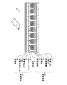
図7は、タッチセンサ部17の一構成例を斜視的に表すものである。タッチセンサ部17は、画素基板20に設けられた駆動電極COML、および対向基板30に設けられたタッチ検出電極TDLにより構成されている。駆動電極COMLは、図7の左右方向に延在する帯状の電極パターンを有している。タッチ検出電極TDLは、駆動電極COMLの電極パターンの延在方向と直交する方向に延びる帯状の電極パターンを有している。タッチ検出電極TDLの各電極パターンは、タッチ検出部18にそれぞれ接続されている。駆動電極COMLとタッチ検出電極TDLにより互いに交差した電極パターンは、その交差部分に静電容量を形成している。
FIG. 7 is a perspective view illustrating a configuration example of the
この構成により、タッチセンサ部17では、駆動電極ドライバ14が駆動電極COMLに対して交流駆動信号VcomACを印加することにより、タッチ検出電極TDLからタッチ検出信号Vdetを出力し、タッチ検出が行われるようになっている。つまり、駆動電極COMLは、図1〜図3に示したタッチ検出の基本原理における駆動電極E1に対応し、タッチ検出電極TDLは、タッチ検出電極E2に対応するものであり、タッチセンサ部17はこの基本原理に従ってタッチを検出するようになっている。図7に示したように、互いに交差した電極パターンは、静電容量式タッチセンサをマトリックス状に構成している。よって、タッチセンサ部17のタッチ検出面全体にわたって走査することにより、外部近接物体の接触または近接が生じた位置の検出も可能となっている。
With this configuration, the
(ゲートドライバ12)
次に、ゲートドライバ12について説明する。ゲートドライバ12は、間欠的に線順次走査することにより、液晶表示部16の1水平ラインを順次選択するものである。
(Gate driver 12)
Next, the
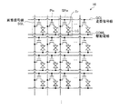
図8は、ゲートドライバ12の一構成例を表すものである。ゲートドライバ12は、走査制御部51と、シフトレジスタ52とを備えている。
FIG. 8 illustrates a configuration example of the
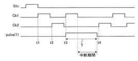
走査制御部51は、制御部11より供給された図示しない制御信号に基づいて、制御信号Stvと、クロック信号Ck1,Ck2と、電位保持信号pulse(1),pulse(2),…を生成し、シフトレジスタ52に対して供給するものである。制御信号Stvは、シフトレジスタ52において転送される信号である。
The
クロック信号Ck1,Ck2は、シフトレジスタ52が信号の転送動作(シフト動作)を行うためのクロック信号である。表示装置1が表示動作を中断してタッチ検出動作を行っている期間において、クロック信号Ck1,Ck2の供給は中断される。以下の説明において、クロック信号Ck1,Ck2の供給が中断される期間を、「中断期間」ということがある。
The clock signals Ck1 and Ck2 are clock signals for the
電位保持信号pulse(1),pulse(2),…は、クロック信号Ck1,Ck2の中断期間に、シフトレジスタ52の構成要素である転送回路50のうち、転送動作によって転送される信号を保持している転送回路50に入力され、その転送回路50に設定されている信号の電位を保つための信号である。電位保持信号pulse(1),pulse(2),…は、電位保持信号線19(1),19(2),…を介して、転送回路50に入力される。
The potential holding signals pulse (1), pulse (2),... Hold signals transferred by the transfer operation in the
シフトレジスタ52は、走査制御部51から供給された制御信号に基づいて、液晶表示部16の各走査信号線GCLに供給される走査信号VG(1),VG(2),…を生成するものである。このシフトレジスタ52は、この例では、図5に示した画素基板20上に、アモルファスシリコンにより形成されている。このシフトレジスタ52は、転送回路50(1),50(2),…を有している。本例では、これら転送回路のうち、転送回路50(4)に電位保持信号pulse(1)が、転送回路50(8)に、電位保持信号pulse(2)が、それぞれ入力されている。
The
以下、走査信号VG(1)等のうちの任意の1つを表すものとして、適宜、走査信号VGを用いる。同様に、転送回路50(1)等のうちの任意の1つを表すものとして、適宜、転送回路50を用いるものとする。同様に、電位保持信号pulse(1)等のうちの任意の1つを表すものとして、適宜、電位保持信号pulseを用いるものとする。同様に、電位保持信号線19(1)等のうちの任意の1つを表すものとして、適宜、電位保持信号線19を用いるものとする。
Hereinafter, the scanning signal VG is used as appropriate to represent any one of the scanning signals VG (1) and the like. Similarly, it is assumed that the
転送回路50は、入力されたシフト信号を一時的に保持し、クロック信号Ck1,Ck2に同期して、シフト信号を次段へ順次伝達するシフト動作を行うと共に、シフト信号を保持している場合にはその出力信号(走査信号VG)を、対応する走査信号線GCLに供給する回路である。ここで、シフト信号は、走査制御部51から供給される信号であり、転送回路50のシフト動作によって次段へ順次伝達される信号である。
The
各転送回路50は、入力端子Ck,Ckbと、入力端子Set,Resetと、出力端子Outとを有している。クロック信号Ck1およびCk2の中断期間にシフト信号を保持する転送回路50には、電位保持信号線19が接続されており、保持されているシフト信号の電位を保つための信号である電位保持信号pulseが中断期間に与えられる。
各転送回路50の入力端子Ckには、クロック信号Ck1,Ck2のうちの一方が、転送回路ごとに交互に供給される。具体的には、例えば、転送回路50(1),50(3),50(5)等の入力端子Ckにはクロック信号Ck1がそれぞれ供給され、転送回路50(2),50(4),50(6)等の入力端子Ckにはクロック信号Ck2がそれぞれ供給される。各転送回路50の入力端子Ckbには、クロック信号Ck1,Ck2のうち、入力端子Ckに入力されたものと異なる信号が供給される。具体的には、例えば、転送回路50(1),50(3),50(5)等の入力端子Ckbにはクロック信号Ck2がそれぞれ供給され、転送回路50(2),50(4),50(6)等の入力端子Ckbにはクロック信号Ck1がそれぞれ供給される。
Each
One of the clock signals Ck1 and Ck2 is alternately supplied to the input terminal Ck of each
各転送回路50の入力端子Setには、図8の例では、着目した転送回路50の上側の転送回路50(つまり、前段の転送回路)の出力信号が供給され、入力端子Resetには、着目した転送回路50の下側の転送回路50(つまり、後段の転送回路)の出力信号が供給される。
In the example of FIG. 8, the output signal of the
各転送回路50は、入力端子Setまたは入力端子Resetに入力された信号を、クロック信号Ck1,Ck2に同期して、出力端子Outから出力する。また、転送回路50は、その出力信号(走査信号VG)を、隣り合う転送回路50に供給すると共に、液晶表示部16の走査信号線GCLに供給するようになっている。
Each
図9は、転送回路50の一構成例を表すものである。転送回路50は、トランジスタTr1〜Tr7と、容量素子C1,C2とを有している。トランジスタTr1〜Tr7は、nチャネルのMOS型のトランジスタである。トランジスタTr7は、ゲートおよびソースが入力端子Setに接続され、ドレインがノードLATに接続されている。トランジスタTr5は、ゲートが入力端子Resetに接続され、ソースが接地端子VGLに接続され、ドレインがノードLATに接続されている。トランジスタTr4は、ゲートがノードLATに接続され、ドレインがノードXLATに接続され、ソースが接地端子VGLに接続されている。トランジスタTr6は、ゲートがノードXLATに接続され、ドレインがノードLATに接続され、ソースが接地端子VGLに接続されている。トランジスタTr2は、ゲートがノードXLATに接続され、ドレインが出力端子Outに接続され、ソースが接地端子VGLに接続されている。トランジスタTr1は、ゲートがノードLATに接続され、ドレインが入力端子Ckに接続され、ソースが出力端子Outに接続されている。トランジスタTr3は、ゲートが入力端子Ckbに接続され、ドレインが出力端子Outに接続され、ソースが接地端子VGLに接続されている。容量素子C2は、一端が入力端子Ckに接続され、他端がノードXLATに接続されている。容量素子C1は、一端がノードLATに接続され、他端が出力端子Outに接続されている。
FIG. 9 illustrates a configuration example of the
このように構成された転送回路50において、容量素子C1に接続されたノードLATがラッチ部として機能し、ノードLATにH電位が保持されている場合に、トランジスタTr1がオン状態になり、出力端子Outから走査信号VGが出力される。なお、以下の説明では、所定閾値より高い電位を「H電位」、所定閾値より低い電位を「L電位」ということがある。
In the
図9に示した例は、クロック信号Ck1およびCk2の中断期間にシフト信号を保持することがない段に配置される転送回路50の構成例である。図9に示した構成の場合、転送回路50がシフト信号を保持している状態、すなわち、ノードLATにH電位が保持されている状態でクロック信号Ck1およびCk2の供給が中断されると、トランジスタのオフリーク等によりノードLATに保持されている電位が低下していく。ノードLATに保持されている電位が低下すると、その転送回路50から出力される走査信号VGの波形がなまって、表示品質が低下するおそれがある。
The example shown in FIG. 9 is a configuration example of the
図10は、クロック信号Ck1およびCk2の中断期間にシフト信号を保持することがある段に配置される転送回路50の一構成例を示す図である。図10に示す転送回路50は、図9に示す転送回路50とは異なり、トランジスタTr7は、ゲートが入力端子Setに接続され、ソースが入力端子Pulseに接続されている。また、トランジスタTr5のソースおよびトランジスタTr6のソースが、入力端子Pulseに接続されている。入力端子Pulseには、その転送回路50に設定されているH電位を保つための電位保持信号pulseが入力される。図10において、その他の構成は、図9を参照して説明した転送回路と同様である。
FIG. 10 is a diagram illustrating a configuration example of the
このような2種類の構成の転送回路50を用いることにより、シフトレジスタ52は、前段の転送回路から供給された信号を、後段の転送回路に転送する。以下に、このシフトレジスタ52の動作について説明する。シフトレジスタ52の、一番上の転送回路50(1)の入力端子Setに、制御信号Stvが供給される。
By using the
以下では、説明を簡略化するため、シフトレジスタ52を構成する転送回路のうち、4段の転送回路50(1),50(2),50(3),50(4)に着目して説明する。すなわち、本例では、1段目の転送回路50(1)から3段目の転送回路50(3)までは、それぞれ、図9を参照して説明した構成になっている。また、4段目の転送回路50(4)は、図10を参照して説明した構成になっている。この4段目の転送回路50(4)には、保持されているH電位を保つための電位保持信号pulse(1)を、中断期間に与えるための電位保持信号線19(1)が接続されている。
In the following, in order to simplify the description, the description will focus on the four stages of transfer circuits 50 (1), 50 (2), 50 (3), and 50 (4) among the transfer circuits constituting the
図11は、シフトレジスタ52の一動作例を表すものである。この例では、シフトレジスタ52における3段目の転送回路50(3)へ、クロック信号Ck1が入力された後、上記の中断期間となる。
FIG. 11 illustrates an operation example of the
まず、シフトレジスタ52の1段目の転送回路50(1)の入力端子Setに入力されている制御信号Stvが立ち上がると、1段目の転送回路50(1)のノードLATがH電位に設定される。その後、転送回路50(1)の入力端子Ckに入力されているクロック信号Ck1が立ち上がるタイミング(L電位からH電位へ遷移するタイミング)t1で、転送回路50(1)の出力端子Outから走査信号VG(1)が出力される。
First, when the control signal Stv input to the input terminal Set of the first stage transfer circuit 50 (1) of the
転送回路50(1)の出力端子Outから出力される信号は、2段目の転送回路50(2)の入力端子Setにも入力される。2段目の転送回路50(2)の入力端子Setに信号が入力されると、2段目の転送回路50(2)のノードLATがH電位に設定される。 The signal output from the output terminal Out of the transfer circuit 50 (1) is also input to the input terminal Set of the second-stage transfer circuit 50 (2). When a signal is input to the input terminal Set of the second-stage transfer circuit 50 (2), the node LAT of the second-stage transfer circuit 50 (2) is set to the H potential.
その後、転送回路50(2)の入力端子Ckに入力されているクロック信号Ck2が立ち上がるタイミングt2で、転送回路50(2)の出力端子Outから走査信号VG(2)が出力される。 Thereafter, the scanning signal VG (2) is output from the output terminal Out of the transfer circuit 50 (2) at the timing t2 when the clock signal Ck2 input to the input terminal Ck of the transfer circuit 50 (2) rises.
転送回路50(2)の出力端子Outから出力される信号は、1段目の転送回路50(1)の入力端子Resetにも入力される。このため、転送回路50(1)のノードLATに設定されていたH電位は解除され、ノードLATはL電位になる。さらに、転送回路50(2)の出力端子Outから出力される信号は、3段目の転送回路50(3)の入力端子Setにも入力される。3段目の転送回路50(3)の入力端子Setに信号が入力されると、3段目の転送回路50(3)のノードLATがH電位に設定される。 The signal output from the output terminal Out of the transfer circuit 50 (2) is also input to the input terminal Reset of the first-stage transfer circuit 50 (1). Therefore, the H potential set at the node LAT of the transfer circuit 50 (1) is released, and the node LAT becomes the L potential. Further, the signal output from the output terminal Out of the transfer circuit 50 (2) is also input to the input terminal Set of the third-stage transfer circuit 50 (3). When a signal is input to the input terminal Set of the third-stage transfer circuit 50 (3), the node LAT of the third-stage transfer circuit 50 (3) is set to the H potential.
その後、転送回路50(3)の入力端子Ckに入力されているクロック信号Ck1が立ち上がるタイミングt3で、転送回路50(3)の出力端子Outから走査信号VG(3)が出力される。 Thereafter, the scanning signal VG (3) is output from the output terminal Out of the transfer circuit 50 (3) at the timing t3 when the clock signal Ck1 input to the input terminal Ck of the transfer circuit 50 (3) rises.
転送回路50(3)の出力端子Outから出力される信号は、2段目の転送回路50(2)の入力端子Resetにも入力される。このため、転送回路50(2)のノードLATに設定されていたH電位は解除され、ノードLATはL電位になる。さらに、転送回路50(3)の出力端子Outから出力される信号は、4段目の転送回路50(4)の入力端子Setにも入力される。4段目の転送回路50(4)の入力端子Setに信号が入力されると、4段目の転送回路50(4)のノードLATがH電位に設定される。 The signal output from the output terminal Out of the transfer circuit 50 (3) is also input to the input terminal Reset of the second-stage transfer circuit 50 (2). For this reason, the H potential set at the node LAT of the transfer circuit 50 (2) is released, and the node LAT becomes the L potential. Further, the signal output from the output terminal Out of the transfer circuit 50 (3) is also input to the input terminal Set of the transfer circuit 50 (4) at the fourth stage. When a signal is input to the input terminal Set of the fourth-stage transfer circuit 50 (4), the node LAT of the fourth-stage transfer circuit 50 (4) is set to the H potential.
ここで、クロック信号Ck1が立ち上がるタイミングt3では、4段目の転送回路50(4)の入力端子Pulseへの電位保持信号pulse(1)が立ち上がり、図11に示す期間Tが終了となるまで電位保持信号pulse(1)は立ち下がらずにH電位が保たれる。図11に示すように、クロック信号の送信が中断されてから再開されるまでの期間が、クロックの中断期間となる。図11に示す期間Tでは、電位保持信号pulse(1)がH電位になるため、転送回路50(4)については、図10中のトランジスタTr7のソースおよびトランジスタTr5のソースがH電位になる。したがって、転送回路50(4)については、図10中のノードLATがH電位に保持される。つまり、入力端子Pulseへの電位保持信号pulse(1)がH電位である期間は、ノードLATに設定されているH電位のリーク経路が無い状態であり、このため、図10中のノードLATがH電位に保持される。 Here, at the timing t3 when the clock signal Ck1 rises, the potential holding signal pulse (1) to the input terminal Pulse of the fourth-stage transfer circuit 50 (4) rises, and the potential until the period T shown in FIG. 11 ends. The holding signal pulse (1) is maintained at the H potential without falling. As shown in FIG. 11, the period from when the transmission of the clock signal is interrupted until it is restarted is the clock interruption period. In the period T shown in FIG. 11, since the potential holding signal pulse (1) becomes the H potential, in the transfer circuit 50 (4), the source of the transistor Tr7 and the source of the transistor Tr5 in FIG. Therefore, for transfer circuit 50 (4), node LAT in FIG. 10 is held at the H potential. That is, the period during which the potential holding signal pulse (1) to the input terminal Pulse is at the H potential is in a state in which there is no leakage path of the H potential set at the node LAT. Therefore, the node LAT in FIG. Hold at H potential.
その後、クロック信号の送信が再開され、転送回路50(4)の入力端子Ckに入力されているクロック信号Ck2が立ち上がるタイミングt4で、転送回路50(4)の出力端子Outから走査信号VG(4)が出力される。電位保持信号pulse(1)により転送回路50(4)のノードLATは、中断期間においてもH電位に保持されるため、転送回路50(4)は、中断期間を経た後であっても、走査信号VG(4)を好適に出力することができる。 Thereafter, the transmission of the clock signal is resumed, and at the timing t4 when the clock signal Ck2 input to the input terminal Ck of the transfer circuit 50 (4) rises, the scanning signal VG (4 ) Is output. Since the node LAT of the transfer circuit 50 (4) is held at the H potential even during the interruption period by the potential holding signal pulse (1), the transfer circuit 50 (4) scans even after the interruption period. The signal VG (4) can be suitably output.
[動作および作用]
続いて、本実施の形態の表示装置1の動作および作用について説明する。
[Operation and Action]
Subsequently, the operation and action of the
(全体動作概要)
まず、図4を参照して、表示装置1の全体動作概要を説明する。制御部11は、表示装置1の外部の制御装置2より供給された映像信号Vdispに基づいて、ゲートドライバ12、ソースドライバ13、駆動電極ドライバ14、およびタッチ検出部18に対してそれぞれ制御信号を供給し、これらがお互いに同期して動作するように制御する。ゲートドライバ12は、タッチセンサ付き表示部15の液晶表示部16に走査信号VGを供給し、表示駆動の対象となる1水平ラインを順次選択する。ソースドライバ13は、画素信号Vsigを、選択された1水平ラインを構成する各サブ画素SPixに供給する。駆動電極ドライバ14は、タッチ検出駆動の対象となる駆動電極COMLに対して交流駆動信号VcomACを順次印加すると共に、それ以外の駆動電極COMLに対して直流駆動信号VcomDCを印加する。タッチセンサ付き表示部15は、表示動作を行うと共にタッチ検出動作を行い、タッチ検出電極TDLからタッチ検出信号Vdetを出力する。タッチ検出部18は、タッチセンサ付き表示部15のタッチセンサ部17から供給されたタッチ検出信号Vdetに基づいて、外部近接物体を検出する。
(Overview of overall operation)
First, with reference to FIG. 4, an outline of the overall operation of the
(詳細動作)
次に、いくつかの図を参照して、表示装置1の動作を詳細に説明する。
(Detailed operation)
Next, the operation of the
図12は、表示装置1の1フレーム期間(1F)における動作を模式的に表すものである。この図12において、横軸は時間を示し、縦軸は表示画面の垂直方向(走査方向)における位置を示す。なお、この図12では、垂直ブランキング期間を省略している。
FIG. 12 schematically shows the operation of the
1フレーム期間(1F)には、表示駆動Ddが行われる表示駆動期間Pdと、タッチ検出駆動Dtが行われるタッチ検出駆動期間Ptとが、交互に配置される。この例では、タッチ検出駆動Dtは、表示駆動Ddの2倍の走査速度で行われる。すなわち、1フレーム期間(1F)の間に、タッチ検出面全面に対するタッチ検出動作が2回行われる。 In one frame period (1F), a display drive period Pd in which the display drive Dd is performed and a touch detection drive period Pt in which the touch detection drive Dt is performed are alternately arranged. In this example, the touch detection drive Dt is performed at a scanning speed twice that of the display drive Dd. That is, the touch detection operation on the entire touch detection surface is performed twice during one frame period (1F).
まず、最初の表示駆動期間Pdにおいて、ゲートドライバ12およびソースドライバ13は、部分表示領域RD(1)を線順次走査により駆動する(表示駆動Dd)。
First, in the first display drive period Pd, the
次に、続くタッチ検出駆動期間Ptにおいて、駆動電極ドライバ14は、タッチ検出駆動の対象となる複数の駆動電極COMLを順次選択して、その選択された駆動電極COMLに対して交流駆動信号VcomACを供給する(タッチ検出駆動Dt)。そして、タッチ検出部18は、その交流駆動信号VcomACに応じてタッチセンサ部17から出力されるタッチ検出信号Vdetに基づいて、外部近接物体を検出する。
Next, in the subsequent touch detection drive period Pt, the drive electrode driver 14 sequentially selects a plurality of drive electrodes COML that are targets of touch detection drive, and supplies an AC drive signal VcomAC to the selected drive electrodes COML. Supply (touch detection drive Dt). And the
同様に、ゲートドライバ12およびソースドライバ13は、続く表示駆動期間Pdにおいて、部分表示領域RD(2)に対して表示駆動Ddを行い、駆動電極ドライバ14は、続くタッチ検出駆動期間Ptにおいて、引き続きタッチ検出駆動Dtを行う。
Similarly, the
このようにして、表示装置1は、1フレーム期間(1F)において、交互に表示駆動Ddとタッチ検出駆動Dtを行うことにより、表示面全面に対する表示動作を行うと共に、タッチ検出面全面に対するタッチ検出動作を行う。これにより、表示装置1では、表示駆動Ddとタッチ検出駆動Dtが、それぞれ別々の期間に行われるため、例えば、表示駆動Ddがタッチ検出動作に与える影響を低減することができる。
In this manner, the
次に、表示駆動期間Pdにおける表示動作と、タッチ検出駆動期間Ptにおけるタッチ検出動作を詳細に説明する。 Next, the display operation in the display drive period Pd and the touch detection operation in the touch detection drive period Pt will be described in detail.
図13は、表示動作のタイミング図を表すものであり、(A)は水平同期信号Ssyncの波形を示し、(B)は走査信号VGの波形を示し、(C)は画素信号Vsigの波形を示し、(D)は駆動信号Vcomの波形を示す。 13A and 13B are timing charts of the display operation. FIG. 13A shows the waveform of the horizontal synchronization signal Ssync, FIG. 13B shows the waveform of the scanning signal VG, and FIG. 13C shows the waveform of the pixel signal Vsig. (D) shows the waveform of the drive signal Vcom.
表示装置1では、表示駆動期間Pdにおいて、駆動電極ドライバ14が、全ての駆動電極COMLに対して直流駆動信号VcomDCを印加し(図13(D))、ゲートドライバ12が、走査信号線GCLに対して、1水平期間(1H)ごとに走査信号VGを順次印加することにより表示走査を行う。以下に、その詳細を説明する。
In the
まず、タイミングt11において、水平同期信号Ssyncにパルスが生じ、1水平期間(1H)が開始する。 First, at a timing t11, a pulse is generated in the horizontal synchronization signal Ssync, and one horizontal period (1H) starts.
次に、タイミングt12において、ゲートドライバ12は、表示動作に係るn行目の走査信号線GCL(n)に対して、走査信号VG(n)を印加し、走査信号VG(n)が低レベルから高レベルに変化する(図13(B))。これにより、ゲートドライバ12は、表示駆動の対象となる1水平ラインを選択する。
Next, at timing t12, the
これと同時に、ソースドライバ13は、画素信号線SGLに対して、画素信号Vsigを印加する(図13(C))。これにより、表示駆動の対象として選択された1水平ラインに属する複数のサブ画素SPixに、画素信号Vsigがそれぞれ印加される。
At the same time, the
次に、ゲートドライバ12は、タイミングt13において、n行目の走査信号線GCLの走査信号VG(n)を高レベルから低レベルに変化させる(図13(B))。これにより、表示動作に係る1水平ラインのサブ画素SPixは、画素信号線SGLから電気的に切り離される。
Next, the
そして、タイミングt14において1水平期間(1H)が終了すると共に、新たな1水平期間(1H)が開始し、次の行(n+1行目)の表示駆動が行われる。 Then, at the timing t14, one horizontal period (1H) ends, and a new one horizontal period (1H) starts, and display driving of the next row (n + 1th row) is performed.
これ以降、上述した動作を繰り返すことにより、表示装置1では、各表示駆動期間Pdにおいて、線順次走査により、部分表示領域RDにおける表示動作が行われる。
Thereafter, by repeating the above-described operation, the
図14は、タッチ検出動作のタイミング図を表すものであり、(A)は駆動信号Vcomの波形を示し、(B)はタッチ検出信号Vdetの波形を示す。 FIG. 14 is a timing chart of the touch detection operation, where (A) shows the waveform of the drive signal Vcom, and (B) shows the waveform of the touch detection signal Vdet.
駆動電極ドライバ14は、タッチ検出駆動期間Ptにおいて、タッチ検出駆動の対象となる複数(この例ではN本)の駆動電極COMLを順次選択して、その選択された駆動電極COMLに対して交流駆動信号VcomACを供給する。この交流駆動信号VcomACは、静電容量を介してタッチ検出電極TDLに伝わり、タッチ検出信号Vdetが変化する(図14(B))。タッチ検出部18は、交流駆動信号VcomACの各パルスに同期したサンプリングタイミングtsにおいて、タッチ検出信号VdetをA/D変換する(図14(B))ことにより、タッチ検出動作を行う。
The drive electrode driver 14 sequentially selects a plurality (N in this example) of drive electrodes COML that are targets of touch detection drive in the touch detection drive period Pt, and performs AC driving on the selected drive electrodes COML. The signal VcomAC is supplied. The AC drive signal VcomAC is transmitted to the touch detection electrode TDL via the capacitance, and the touch detection signal Vdet changes (FIG. 14B). The
(ゲートドライバ12の詳細動作)
図15は、ゲートドライバ12の一動作例を表すものであり、(A)は制御信号Stvの波形を示し、(B)はクロック信号Ck1の波形を示し、(C)はクロック信号Ck2の波形を示し、(D)は走査信号VG(1)〜VG(4)の波形を示し、(E)は走査信号VG(5)〜VG(8)の波形を示し、(F)は走査信号VG(9)の波形を示す。
(Detailed operation of the gate driver 12)
FIG. 15 illustrates an operation example of the
ゲートドライバ12は、表示駆動期間Pdにおいて走査信号VGを次々に生成して液晶表示部16に供給する。一方、タッチ検出駆動期間Ptでは、ゲートドライバ12は、走査信号VGの生成を停止する。ゲートドライバ12は、このような走査信号VGの生成を、クロック信号Ck1,Ck2により制御する。
The
まず、走査制御部51が、タイミングt20に立ち上がりタイミングt21に立ち下がる制御信号Stvを生成する(図15(A))。そして、シフトレジスタ52の最初の転送回路50(1)は、この制御信号Stvをクロック信号Ck1(図15(B))に同期して転送することにより、走査信号VG(1)を生成する(図15(D))。そして、転送回路50(2)は、走査信号VG(1)をクロック信号Ck2(図15(C))に同期して転送することにより、走査信号VG(2)を生成する(図15(D))。同様に、転送回路50(3),50(4)は、入力された信号をそれぞれ転送し、走査信号VG(3),VG(4)を生成する(図15(D))。このように、転送回路50(1)〜50(4)は、表示駆動期間Pdにおいて、走査信号VG(1)〜VG(4)を生成し、液晶表示部16に供給する。
First, the
そして、走査制御部51は、タイミングt22において、クロック信号Ck1,Ck2の生成を停止した後、タイミングt23において、これらの生成を再開する(図15(B),(C))。次段以降の転送回路50(5)〜50(8)は、タイミングt23以降に引き続き現れるクロック信号Ck1,Ck2のパルスに同期して、入力された信号をそれぞれ同様に転送する(図15(E))。すなわち、タッチ検出駆動期間Ptでは、走査制御部51は、クロック信号Ck1,Ck2の生成を停止し、その後にこれらの生成を再開して、最初のパルスを生成する。そして、走査制御部51は、続く表示駆動期間Pdにおいて、クロック信号Ck1,Ck2を生成し続け、転送回路50(5)〜50(8)が、走査信号VG(5)〜VG(8)を生成し、液晶表示部16に供給する。
Then, after stopping the generation of the clock signals Ck1 and Ck2 at the timing t22, the
そして、走査制御部51は、タイミングt24において、クロック信号Ck1,Ck2の生成を停止した後、タイミングt25において、これらの生成を再開する(図15(B),(C))。
Then, after stopping the generation of the clock signals Ck1 and Ck2 at the timing t24, the
このように、ゲートドライバ12は、タッチ検出駆動期間Ptにおいて、クロック信号Ck1,Ck2の生成を一旦停止することにより、走査信号VGの生成を停止する。
Thus, the
[効果]
以上のように本実施の形態では、回路動作をとめている期間、電位保持信号を入力してリーク経路になる配線の電圧をH電位に設定することにより、充電したH電位が低下しないようにして、画質の低下を抑えることができる。
[effect]
As described above, in this embodiment, during the period when the circuit operation is stopped, the potential holding signal is input and the voltage of the wiring that becomes the leakage path is set to the H potential so that the charged H potential does not decrease. Therefore, it is possible to suppress a decrease in image quality.
[変形例1]
上記したように、本例の表示装置1では、シフトレジスタ52を構成する複数段の転送回路のうち、中断期間にシフト信号を保持することがある段に配置される転送回路に、電位保持信号を入力する。このため、例えば、複数段の転送回路について、所定段数(回路数)ごとに電位保持信号が入力される。上記の例では4段ごと(4回路ごと)に電位保持信号を入力しているが、4段(4回路)よりも少ない段ごとまたは4段(4回路)よりも多い段ごとに電位保持信号を入力してもよい。
[Modification 1]
As described above, in the
[変形例2]
図8では、中断期間にシフト信号を保持することがある転送回路(図10に示した構成の転送回路)ごとに電位保持信号線19を独立して設ける例を示した。しかしながら、シフトレジスタの構成は、これに限定されない。例えば、図16に示すように、図10に示した構成の転送回路の全てが、1つの電位保持信号線19を共用してもよい。すなわち、シフトレジスタは、中断期間において、図10に示した構成の転送回路の全てに電位保持信号pulseが入力されるように構成されてもよい。
[Modification 2]
FIG. 8 shows an example in which the potential
中断期間において、図10に示した構成の転送回路の全てに電位保持信号pulseを入力する場合、図17に示すように、走査信号を現在出力している転送回路以外は、入力端子Pulseへの電位保持信号pulseがH電位で、ノードLATがL電位になる。Set端子及びReset端子はL電位である。また、図17に示すように、電位保持信号pulseがH電位(図17中のH)であれば、オフリーク電流によりノードLATの電圧が上昇する可能性がある。 When the potential holding signal pulse is input to all the transfer circuits having the configuration shown in FIG. 10 during the interruption period, as shown in FIG. 17, except for the transfer circuit that is currently outputting the scanning signal, the transfer to the input terminal Pulse is performed. The potential holding signal pulse is at the H potential and the node LAT is at the L potential. The Set terminal and the Reset terminal are at the L potential. Further, as shown in FIG. 17, if the potential holding signal pulse is an H potential (H in FIG. 17), the voltage of the node LAT may increase due to an off-leakage current.
しかしながら、この構成であっても、例えば、図9に示した構成の転送回路のみを用いたシフトレジスタの構成と比較して、ノードLATが電流リークによってH電位から低下してL電位になるまでの時間よりも長くすることができ、動作マージンが大きい。 However, even with this configuration, for example, as compared with the configuration of the shift register using only the transfer circuit having the configuration shown in FIG. 9, the node LAT decreases from the H potential to the L potential due to current leakage. The operation margin can be made longer than the above-mentioned time, and the operation margin is large.
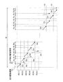
図18に、光照射時のTFTの動作特性の一例を示す。図18において、横軸はゲート−ソース間電圧Vgs[V]、縦軸はソース電流IS[A]であり、実際の回路を構成するTFTを測定したものである。なお、測定の際には表示部のバックライトを7000カンデラ/m2とし、TFTの表面を遮光した状態で、ソース電圧VS=5.1[V]を印加している。
FIG. 18 shows an example of operating characteristics of the TFT during light irradiation. In FIG. 18, the horizontal axis represents the gate-source voltage Vgs [V], and the vertical axis represents the source current IS [A], which is obtained by measuring the TFT constituting the actual circuit. At the time of measurement, the source voltage VS = 5.1 [V] is applied in a state where the backlight of the display portion is set to 7000 candela /
図18において、ゲート−ソース間電圧Vgs=0[V]付近では、ゲート−ソース間電圧Vgsの変化によってソース電流ISは急激に変化する。 In FIG. 18, near the gate-source voltage Vgs = 0 [V], the source current IS changes rapidly due to the change of the gate-source voltage Vgs.
ここで、図9の転送回路でノードLATが電流リークによってH電位から低下してL電位になる場合、ノードLATにつながるトランジスタTr5,Tr6,およびTr7のゲート−ソース間電圧VgsはノードLATの電位によらず0[V]である。このため、電流がリークしても動作点は図18のゲート−ソース間電圧Vgs=0[V]であり、電流リーク量は大きい。 Here, in the transfer circuit of FIG. 9, when the node LAT drops from the H potential to the L potential due to current leakage, the gate-source voltage Vgs of the transistors Tr5, Tr6, and Tr7 connected to the node LAT is the potential of the node LAT. Regardless, it is 0 [V]. Therefore, even if the current leaks, the operating point is the gate-source voltage Vgs = 0 [V] in FIG. 18, and the amount of current leak is large.
一方、図10の転送回路の場合、初期はゲート−ソース間電圧Vgs=0[V]だが、ノードLATが持ち上がってくると、動作点はゲート−ソース間電圧Vgs=0[V]以下になり、トランジスタTr5,Tr6,およびTr7の電流リーク量は大きく減少する。したがって、図10の転送回路の構成によれば、図9の転送回路よりもクロック信号の中断期間を長く設定することができると考えられる。 On the other hand, in the case of the transfer circuit of FIG. 10, the gate-source voltage Vgs = 0 [V] in the initial stage, but when the node LAT is lifted, the operating point becomes the gate-source voltage Vgs = 0 [V] or less. The current leakage amount of the transistors Tr5, Tr6, and Tr7 is greatly reduced. Therefore, according to the configuration of the transfer circuit in FIG. 10, it is considered that the interruption period of the clock signal can be set longer than that in the transfer circuit in FIG.
発明者が行ったシミュレーションではノードLATの電圧値が上昇しても電圧値が3[V]までは、ゲート電圧がL電位を保った。図18の波形を参照すると、ゲート−ソース間電圧Vgs=0[V]で8E−8[A]のリーク電流が流れるとする。図9の転送回路の場合ではノードLATの電圧を2[V]の変動以下に抑えるなら、停止時間tはノードLATの容量を4[pF]として以下の式(1)のようになる。 In the simulation conducted by the inventor, even when the voltage value of the node LAT is increased, the gate voltage is maintained at the L potential until the voltage value reaches 3 [V]. Referring to the waveform of FIG. 18, it is assumed that a leak current of 8E-8 [A] flows when the gate-source voltage Vgs = 0 [V]. In the case of the transfer circuit of FIG. 9, if the voltage at the node LAT is suppressed to 2 V or less, the stop time t is expressed by the following equation (1) with the capacity of the node LAT being 4 [pF].
t=4[pF]*2[V]/8E−8[A]=100[μs] …(1) t = 4 [pF] * 2 [V] / 8E-8 [A] = 100 [μs] (1)
一方、図10の場合、動作点が少しマイナス側に行ってもよいとして、リーク電流が2E−8[A]とすると、停止時間tはノードLATの容量を4[pF]として以下の式(2)のようになる。 On the other hand, in the case of FIG. 10, assuming that the operating point may be slightly negative, assuming that the leakage current is 2E-8 [A], the stop time t is set to 4 [pF] and the following equation ( 2).
t=4[pF]*2[V]/2E−8[A]=400[μs] …(2) t = 4 [pF] * 2 [V] / 2E-8 [A] = 400 [μs] (2)
したがって、図9の構成を採用するよりも図10の構成を採用する方がクロックの中断期間を長く取ることができる。 Therefore, it is possible to take a longer clock interruption period when the configuration of FIG. 10 is employed than when the configuration of FIG. 9 is employed.
[変形例3]
アモルファスシリコン(a−Si)によるトランジスタは、ゲートにプラス(+)電圧を印加するとしきい値電圧Vthがプラス方向にシフトし、マイナス(−)電圧を印加するとしきい値電圧Vthがマイナス方向にシフトする。そして、しきい値電圧Vthがマイナスにシフトして、トランジスタがデプレション型になることがある。
[Modification 3]
In a transistor made of amorphous silicon (a-Si), the threshold voltage Vth shifts in the positive direction when a positive (+) voltage is applied to the gate, and the threshold voltage Vth in the negative direction when a negative (-) voltage is applied. shift. Then, the threshold voltage Vth may shift to a negative value, and the transistor may become a depletion type.
ここで、上述したトランジスタTr7はゲートがチャネルに対してマイナスになるタイミングはあっても、プラスになるタイミングは無く、デプレション型になる可能性がある。これを防止するために、図11のタイミングチャートにおいて、クロック信号Ck1の立ち上がりタイミングよりも電位保持信号pulseの立ち上がりタイミングを若干遅くする。すなわち、図19のように、クロック信号Ck1の立ち上がりタイミングt3よりも、電位保持信号pulseの立ち上がりタイミングt3’を若干遅くする。すると、トランジスタTr7のゲートはH電位で、チャネルはL電位のタイミングができるので、しきい値電圧Vthのマイナス方向へのシフトを抑えることができる。 Here, although the transistor Tr7 described above has a timing at which the gate becomes negative with respect to the channel, there is no timing at which the gate becomes positive, and there is a possibility that the transistor Tr7 becomes a depletion type. In order to prevent this, the rising timing of the potential holding signal pulse is slightly delayed from the rising timing of the clock signal Ck1 in the timing chart of FIG. That is, as shown in FIG. 19, the rising timing t3 'of the potential holding signal pulse is slightly delayed from the rising timing t3 of the clock signal Ck1. Then, since the gate of the transistor Tr7 can be at the H potential and the channel can be at the L potential, the shift of the threshold voltage Vth in the negative direction can be suppressed.
<3.適用例>
次に、上記実施の形態および変形例で説明した表示装置の適用例について説明する。図20〜図32は、実施の形態等の表示装置が適用される電子機器の外観例を表す図である。上記実施の形態等の表示装置は、テレビジョン装置、デジタルカメラ、ノート型パーソナルコンピュータ、携帯電話等の携帯端末装置あるいはビデオカメラなどのあらゆる分野の電子機器に適用することが可能である。言い換えると、上記実施の形態等の表示装置は、外部から入力された映像信号あるいは内部で生成した映像信号を、画像あるいは映像として表示するあらゆる分野の電子機器に適用することが可能である。
<3. Application example>
Next, application examples of the display device described in the above embodiment and modifications will be described. 20 to 32 are diagrams illustrating an external appearance example of an electronic device to which the display device according to the embodiment or the like is applied. The display device in the above embodiment and the like can be applied to electronic devices in various fields such as a television device, a digital camera, a laptop personal computer, a mobile terminal device such as a mobile phone, or a video camera. In other words, the display device according to the above-described embodiment or the like can be applied to electronic devices in various fields that display an externally input video signal or an internally generated video signal as an image or video.
(適用例1)
図20に示す電子機器は、上記実施の形態等の表示装置が適用されるテレビジョン装置である。このテレビジョン装置は、例えば、フロントパネル511及びフィルターガラス512を含む映像表示画面部510を有しており、この映像表示画面部510は、上記実施の形態等の表示装置である。
(Application example 1)
An electronic device illustrated in FIG. 20 is a television device to which the display device according to any of the above embodiments is applied. This television apparatus has, for example, a video display screen unit 510 including a
(適用例2)
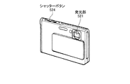
図21及び図22に示す電子機器は、上記実施の形態等の表示装置が適用されるデジタルカメラである。このデジタルカメラは、例えば、フラッシュ用の発光部521、表示部522、メニュースイッチ523及びシャッターボタン524を有しており、その表示部522は、上記実施の形態等の表示装置である。
(Application example 2)
The electronic device illustrated in FIGS. 21 and 22 is a digital camera to which the display device of the above-described embodiment or the like is applied. The digital camera includes, for example, a flash
(適用例3)
図23に示す電子機器は、上記実施の形態等の表示装置が適用されるビデオカメラの外観を表すものである。このビデオカメラは、例えば、本体部531、この本体部531の前方側面に設けられた被写体撮影用のレンズ532、撮影時のスタート/ストップスイッチ533及び表示部534を有している。そして、表示部534は、上記の実施形態及び変形例に係る表示装置ある。
(Application example 3)
The electronic device illustrated in FIG. 23 represents an appearance of a video camera to which the display device according to any of the above embodiments is applied. This video camera has, for example, a
(適用例4)
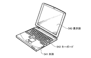
図24に示す電子機器は、上記実施の形態等の表示装置が適用されるノート型パーソナルコンピュータである。このノート型パーソナルコンピュータは、例えば、本体541、文字等の入力操作のためのキーボード542及び画像を表示する表示部543を有しており、表示部543は、上記実施の形態等の表示装置である。
(Application example 4)
An electronic device illustrated in FIG. 24 is a laptop personal computer to which the display device according to any of the above embodiments is applied. The notebook personal computer includes, for example, a main body 541, a keyboard 542 for inputting characters and the like, and a display unit 543 for displaying an image. The display unit 543 is a display device such as the above embodiment. is there.
(適用例5)
図25〜図31に示す電子機器は、上記実施の形態等の表示装置が適用される携帯電話機である。この携帯電話機は、例えば、上側筐体551と下側筐体552とを連結部(ヒンジ部)553で連結したものであり、ディスプレイ554、サブディスプレイ555、ピクチャーライト556及びカメラ557を有している。そのディスプレイ554又はサブディスプレイ555は、上記の実施形態及び変形例に係る表示装置である。
(Application example 5)
Electronic devices shown in FIGS. 25 to 31 are cellular phones to which the display device of the above-described embodiment or the like is applied. This mobile phone is, for example, one in which an
(適用例6)
図32に示す電子機器は、携帯型コンピュータ、多機能な携帯電話、音声通話可能な携帯コンピュータ又は通信可能な携帯コンピュータとして動作し、いわゆるスマートフォン、タブレット端末と呼ばれることもある、情報携帯端末である。この情報携帯端末は、例えば筐体561の表面に表示部562を有している。この表示部562は、上記実施の形態等の表示装置である。
(Application example 6)
The electronic device illustrated in FIG. 32 is an information portable terminal that operates as a portable computer, a multifunctional portable phone, a portable computer capable of voice communication, or a portable computer capable of communication, and is sometimes referred to as a so-called smartphone or tablet terminal. . This information portable terminal has a
以上、実施の形態および電子機器への適用例を挙げて本技術を説明したが、本技術はこれらの実施の形態等には限定されず、種々の変形が可能である。 As described above, the present technology has been described with reference to the embodiments and application examples to the electronic apparatus. However, the present technology is not limited to these embodiments and the like, and various modifications are possible.
例えば、上記実施の形態等では、FFSやIPS等の横電界モードの液晶を用いた液晶表示部16とタッチセンサ部17とを一体化したが、これに代えて、TN(ツイステッドネマティック)、VA(垂直配向)、ECB(電界制御複屈折)等の各種モードの液晶を用いた液晶表示部とタッチセンサ部17とを一体化してもよい。このような液晶を用いた場合には、タッチセンサ付き表示部を、図33に示したように構成可能である。図33は、本変形例に係るタッチセンサ付き表示部15Bの要部断面構造の一例を表すものであり、画素基板20Bと対向基板30Bとの間に液晶層9Bを挟持された状態を示している。その他の各部の名称や機能等は図5の場合と同様なので、説明を省略する。この例では、図5の場合とは異なり、表示用とタッチ検出用の双方に兼用される駆動電極COMLは、対向基板30Bに形成されている。
For example, in the above-described embodiment, the liquid
また、例えば、上記実施の形態等では、タッチセンサは静電容量式としたが、これに限定されるものではなく、これに代えて、例えば光学式であってもよいし、抵抗膜式であってもよい。 Further, for example, in the above-described embodiment, the touch sensor is a capacitive type, but is not limited to this, and instead, for example, an optical type or a resistive film type may be used. There may be.
また、例えば、上記実施の形態等では、表示素子は液晶素子としたが、これに限定されるものではなく、これに代えて、例えばEL(Electro Luminescence)素子であってもよい。 Further, for example, in the above-described embodiment and the like, the display element is a liquid crystal element. However, the display element is not limited to this, and instead, for example, an EL (Electro Luminescence) element may be used.
また、例えば、上記実施の形態等では、液晶表示部16とタッチセンサ部17とを組み合わせ、液晶表示部16における表示動作と、タッチセンサ部17におけるタッチ検出動作とが互いに影響しないように、それぞれ別々の期間(表示駆動期間Pdおよびタッチ検出駆動期間Pt)に動作するようにしたが、これに限定されるものではない。これに代えて、例えば、液晶表示部16と無線通信部とを組み合わせ、液晶表示部16における表示動作と、無線通信部における無線通信動作とが互いに影響しないように、それぞれ別々の期間(表示駆動期間Pdおよび無線通信期間)に動作するようにしてもよい。
Further, for example, in the above-described embodiment, the liquid
なお、本技術は以下のような構成とすることができる。 In addition, this technique can be set as the following structures.
(1)走査信号が印加される複数の走査信号線を有する表示部と、
入力されたシフト信号を一時的に保持し、中断期間を有するクロック信号に同期して、該シフト信号を次段へ順次伝達するシフト動作を行う複数段の転送回路を有し、前記シフト信号を保持する転送回路に対応する走査信号線へ前記走査信号を出力するシフトレジスタと、
前記クロック信号の前記中断期間に、前記シフト信号を保持する転送回路に該シフト信号の電位を保持するための電位保持信号を伝達する信号線と、
を含む表示装置。
(1) a display unit having a plurality of scanning signal lines to which a scanning signal is applied;
It has a plurality of transfer circuits that temporarily hold the input shift signal and perform a shift operation for sequentially transmitting the shift signal to the next stage in synchronization with a clock signal having an interruption period. A shift register that outputs the scanning signal to a scanning signal line corresponding to a transfer circuit to be held;
A signal line for transmitting a potential holding signal for holding the potential of the shift signal to a transfer circuit for holding the shift signal during the interruption period of the clock signal;
Display device.
(2)前記複数段の転送回路は、前記中断期間に前記シフト信号を保持することがある段に配置される第1転送回路と、前記中断期間に前記シフト信号を保持することがない段に配置される第2転送回路と、を含む
前記(1)に記載の表示装置。
(2) The plurality of stages of transfer circuits include a first transfer circuit arranged in a stage that may hold the shift signal during the interruption period, and a stage that does not hold the shift signal during the interruption period. A display device according to (1), including a second transfer circuit disposed.
(3)前記転送回路は、前段の転送回路が出力する前記シフト信号および前記電位保持信号によって前記電位が設定され、かつ、設定された前記電位が次段の転送回路が出力するシフト信号によって解除されるラッチ部と、前記ラッチ部によって保持される前記電位によってオン状態になり、前記クロック信号を前記シフト信号として出力する第1スイッチ部とを備え、
前記ラッチ部は、前記電位保持信号が入力されている期間において、電流リーク経路の電位を当該電位保持信号によって保つ、
前記(1)または(2)に記載の表示装置。
(3) In the transfer circuit, the potential is set by the shift signal and the potential holding signal output from the previous transfer circuit, and the set potential is canceled by the shift signal output from the next-stage transfer circuit. And a first switch unit that is turned on by the potential held by the latch unit and outputs the clock signal as the shift signal.
The latch unit maintains the potential of the current leakage path by the potential holding signal during a period in which the potential holding signal is input.
The display device according to (1) or (2).
(4)前記転送回路は、前段の転送回路が出力する前記シフト信号によってオン状態になって前記ラッチ部に前記電位を設定するための第2スイッチ部と、後段の転送回路が出力するシフト信号によってオン状態になって前記ラッチ部に設定されている前記電位を解除する第3スイッチ部とを備え、
前記ラッチ部は、前記電位保持信号によって前記第2スイッチ部を介して前記電位が設定されている期間において、前記第3スイッチ部を通る電流リーク経路の電位を当該電位保持信号によって保つ
前記(3)に記載の表示装置。
(4) The transfer circuit is turned on by the shift signal output from the preceding transfer circuit and is set to the second switch unit for setting the potential in the latch unit, and the shift signal output from the subsequent transfer circuit. And a third switch unit that is turned on by the latch unit to release the potential set in the latch unit,
The latch unit maintains the potential of the current leakage path passing through the third switch unit by the potential holding signal during a period in which the potential is set via the second switch unit by the potential holding signal. ) Display device.
(5)前記電位保持信号が立ち上がるタイミングは、前記クロック信号が立ち上がるタイミングより遅く設定されている、
前記(1)から(4)までのいずれか1つに記載の表示装置。
(5) The timing at which the potential holding signal rises is set later than the timing at which the clock signal rises.
The display device according to any one of (1) to (4).
(6)前記第1転送回路の数は複数であり、
前記信号線は、前記第1転送回路毎に設けられる
前記(1)から(5)までのいずれか1つに記載の表示装置。
(6) The number of the first transfer circuits is plural,
The display device according to any one of (1) to (5), wherein the signal line is provided for each of the first transfer circuits.
(7)接触または近接を検出するタッチセンサ部をさらに備え、
前記クロック信号の中断期間は、前記タッチセンサ部が前記接触または前記近接を検出するための期間として設定されている、前記(1)から(6)までのいずれか1つに記載の表示装置。
(7) It further includes a touch sensor unit that detects contact or proximity,
The display device according to any one of (1) to (6), wherein the interruption period of the clock signal is set as a period for the touch sensor unit to detect the contact or the proximity.
(8)前記(1)から(7)までのいずれかに記載の表示装置と、
前記表示装置に入力信号を供給する制御装置と、を有する電子機器。
(8) The display device according to any one of (1) to (7),
And a control device that supplies an input signal to the display device.
1 表示装置
11 制御部
12 ゲートドライバ
13 ソースドライバ
14 駆動電極ドライバ
15 タッチセンサ付き表示部
16 液晶表示部
17 タッチセンサ部
18 タッチ検出部
19 電位保持信号線
20 画素基板
21 TFT基板
22 画素電極
23 絶縁層
30 対向基板
31 ガラス基板
32 カラーフィルタ
35 偏光板
50 転送回路
51 走査制御部
52 シフトレジスタ
DESCRIPTION OF
Claims (8)
入力されたシフト信号を一時的に保持し、中断期間を有するクロック信号に同期して、該シフト信号を次段へ順次伝達するシフト動作を行う複数段の転送回路を有し、前記シフト信号を保持する転送回路に対応する走査信号線へ前記走査信号を出力するシフトレジスタと、
前記クロック信号の前記中断期間に、前記シフト信号を保持する転送回路に該シフト信号の電位を保持するための電位保持信号を伝達する信号線と、
を含む表示装置。 A display unit having a plurality of scanning signal lines to which the scanning signal is applied;
It has a plurality of transfer circuits that temporarily hold the input shift signal and perform a shift operation for sequentially transmitting the shift signal to the next stage in synchronization with a clock signal having an interruption period. A shift register that outputs the scanning signal to a scanning signal line corresponding to a transfer circuit to be held;
A signal line for transmitting a potential holding signal for holding the potential of the shift signal to a transfer circuit for holding the shift signal during the interruption period of the clock signal;
Display device.
前記ラッチ部は、前記電位保持信号が入力されている期間において、電流リーク経路の電位を当該電位保持信号によって保つ請求項1または2に記載の表示装置。 The transfer circuit is a latch in which the potential is set by the shift signal and the potential holding signal output from the previous transfer circuit, and the set potential is released by the shift signal output by the next transfer circuit. And a first switch unit that is turned on by the potential held by the latch unit and outputs the clock signal as the shift signal,
The display device according to claim 1, wherein the latch unit maintains the potential of the current leakage path by the potential holding signal during a period in which the potential holding signal is input.
前記ラッチ部は、前記電位保持信号によって前記第2スイッチ部を介して前記電位が設定されている期間において、前記第3スイッチ部を通る電流リーク経路の電位を当該電位保持信号によって保つ請求項3に記載の表示装置。 The transfer circuit is turned on by the shift signal output from the preceding transfer circuit and is turned on by the second switch unit for setting the potential in the latch unit and the shift signal output from the succeeding transfer circuit. And a third switch part for releasing the potential set in the latch part,
The latch unit maintains a potential of a current leak path passing through the third switch unit by the potential holding signal during a period in which the potential is set via the second switch unit by the potential holding signal. The display device described in 1.
前記信号線は、前記第1転送回路毎に設けられる請求項1から請求項5までのいずれか1項に記載の表示装置。 The number of the first transfer circuits is plural,
The display device according to claim 1, wherein the signal line is provided for each first transfer circuit.
前記クロック信号の中断期間は、前記タッチセンサ部が前記接触または前記近接を検出するための期間として設定されている、請求項1から請求項6までのいずれか1項に記載の表示装置。 A touch sensor for detecting contact or proximity;
The display device according to claim 1, wherein the interruption period of the clock signal is set as a period for the touch sensor unit to detect the contact or the proximity.
前記表示装置に入力信号を供給する制御装置と、を有する電子機器。 A display device according to any one of claims 1 to 7,
And a control device that supplies an input signal to the display device.
Priority Applications (3)
| Application Number | Priority Date | Filing Date | Title |
|---|---|---|---|
| JP2013055243A JP2014182203A (en) | 2013-03-18 | 2013-03-18 | Display device, and electronic equipment |
| US14/201,128 US9619087B2 (en) | 2013-03-18 | 2014-03-07 | Display device and electronic apparatus |
| US15/448,169 US10606384B2 (en) | 2013-03-18 | 2017-03-02 | Display device and electronic apparatus |
Applications Claiming Priority (1)
| Application Number | Priority Date | Filing Date | Title |
|---|---|---|---|
| JP2013055243A JP2014182203A (en) | 2013-03-18 | 2013-03-18 | Display device, and electronic equipment |
Publications (1)
| Publication Number | Publication Date |
|---|---|
| JP2014182203A true JP2014182203A (en) | 2014-09-29 |
Family
ID=51525326
Family Applications (1)
| Application Number | Title | Priority Date | Filing Date |
|---|---|---|---|
| JP2013055243A Pending JP2014182203A (en) | 2013-03-18 | 2013-03-18 | Display device, and electronic equipment |
Country Status (2)
| Country | Link |
|---|---|
| US (2) | US9619087B2 (en) |
| JP (1) | JP2014182203A (en) |
Cited By (17)
| Publication number | Priority date | Publication date | Assignee | Title |
|---|---|---|---|---|
| KR20170066443A (en) | 2014-12-05 | 2017-06-14 | 도판 인사츠 가부시키가이샤 | Display device substrate, method for manufacturing display device substrate, and display device using same |
| KR20180003701A (en) * | 2016-06-30 | 2018-01-10 | 엘지디스플레이 주식회사 | Display Device Having Touch Sensor |
| JP2018508854A (en) * | 2015-01-05 | 2018-03-29 | 深▲セン▼市華星光電技術有限公司 | Display panel having touch function and touch detection method |
| JP2018092161A (en) * | 2016-11-25 | 2018-06-14 | 株式会社半導体エネルギー研究所 | Display device and operating method thereof |
| KR20180079413A (en) | 2015-12-28 | 2018-07-10 | 도판 인사츠 가부시키가이샤 | Liquid crystal display |
| KR20180126594A (en) | 2016-05-13 | 2018-11-27 | 도판 인사츠 가부시키가이샤 | Display device |
| JP2018536182A (en) * | 2015-09-28 | 2018-12-06 | 深▲せん▼市華星光電技術有限公司Shenzhen China Star Optoelectronics Technology Co., Ltd. | Display device, TFT substrate and GOA drive circuit |
| JP2019502148A (en) * | 2015-11-09 | 2019-01-24 | 武漢華星光電技術有限公司 | GOA drive circuit, TFT display panel and display device |
| WO2019017264A1 (en) * | 2017-07-19 | 2019-01-24 | シャープ株式会社 | Shift register and display device provided with same |
| JP2019061323A (en) * | 2017-09-25 | 2019-04-18 | 株式会社ジャパンディスプレイ | Display device |
| US10296121B2 (en) | 2015-07-09 | 2019-05-21 | Sharp Kabushiki Kaisha | Shift register, display device provided with same, and shift register driving method |
| US10629147B2 (en) | 2017-09-11 | 2020-04-21 | Sharp Kabushiki Kaisha | Display device |
| US10679578B2 (en) | 2017-09-28 | 2020-06-09 | Sharp Kabushiki Kaisha | Display device having driving circuitry with driving gate lines |
| US10777156B2 (en) | 2017-09-01 | 2020-09-15 | Sharp Kabushiki Kaisha | Display driving device and display device having electric potential controlling circuitry |
| US10902813B2 (en) | 2017-11-15 | 2021-01-26 | Sharp Kabushiki Kaisha | Shift register and display device provided with same |
| US10964244B2 (en) | 2018-09-04 | 2021-03-30 | Sharp Kabushiki Kaisha | Display device |
| US11094278B2 (en) | 2015-02-12 | 2021-08-17 | Japan Display Inc. | Display apparatus including a substrate with first and second regions including respective first and second circuit portions with different dimensions |
Families Citing this family (12)
| Publication number | Priority date | Publication date | Assignee | Title |
|---|---|---|---|---|
| US9842551B2 (en) * | 2014-06-10 | 2017-12-12 | Apple Inc. | Display driver circuitry with balanced stress |
| CN104537972B (en) * | 2014-12-26 | 2017-05-31 | 厦门天马微电子有限公司 | Drive circuit, touch-control display panel and touch control display apparatus |
| CN104485080B (en) * | 2014-12-31 | 2017-02-22 | 深圳市华星光电技术有限公司 | GOA (Gate Driver On Array) circuit for liquid crystal display device |
| CN104505014B (en) * | 2014-12-31 | 2017-02-22 | 厦门天马微电子有限公司 | Drive circuit, array substrate and touch display device as well as drive method thereof |
| CN104485082B (en) * | 2014-12-31 | 2017-02-22 | 厦门天马微电子有限公司 | Array substrate, touch control display device and drive method of touch control display device |
| CN104808862B (en) * | 2015-05-14 | 2018-02-23 | 厦门天马微电子有限公司 | The driving method of array base palte, touch-control display panel and array base palte |
| US10365751B2 (en) * | 2015-07-10 | 2019-07-30 | Tpk Touch Solutions (Xiamen) Inc. | Display device with three-dimension input module |
| CN110111754B (en) * | 2015-07-17 | 2021-08-10 | 群创光电股份有限公司 | Gate drive circuit |
| CN105183224B (en) * | 2015-09-07 | 2018-08-07 | 厦门天马微电子有限公司 | Driving circuit, touch-control display panel and touch control display apparatus |
| US10579197B2 (en) | 2015-12-31 | 2020-03-03 | Egalax_Empia Technology Inc. | Touch sensitive processing method |
| TWI638298B (en) * | 2015-12-31 | 2018-10-11 | 禾瑞亞科技股份有限公司 | Touch sensitive controlling method, touch sensitive processing system and electronic device |
| JP2019090927A (en) * | 2017-11-15 | 2019-06-13 | シャープ株式会社 | Scan signal line drive circuit and display device including the same |
Citations (3)
| Publication number | Priority date | Publication date | Assignee | Title |
|---|---|---|---|---|
| JP2000338919A (en) * | 1999-03-25 | 2000-12-08 | Seiko Epson Corp | Driving circuit for electro-optic device, electro-optic device, and projection type display device |
| JP2007317288A (en) * | 2006-05-25 | 2007-12-06 | Mitsubishi Electric Corp | Shift register circuit and image display equipped therewith |
| WO2012137800A1 (en) * | 2011-04-08 | 2012-10-11 | シャープ株式会社 | Display device, method for driving same, and electronic apparatus |
Family Cites Families (5)
| Publication number | Priority date | Publication date | Assignee | Title |
|---|---|---|---|---|
| KR20100083370A (en) * | 2009-01-13 | 2010-07-22 | 삼성전자주식회사 | Gate driving circuit and display device having the same |
| JP2010250030A (en) | 2009-04-15 | 2010-11-04 | Sharp Corp | Shift register, display device equipped with the same, and method of driving shift register |
| WO2011007591A1 (en) * | 2009-07-15 | 2011-01-20 | シャープ株式会社 | Scan signal line driving circuit and display apparatus having same |
| JP5191522B2 (en) | 2010-10-29 | 2013-05-08 | 三菱電機株式会社 | Shift register circuit |
| CN102750062B (en) * | 2012-06-29 | 2016-02-10 | 京东方科技集团股份有限公司 | A kind of capacitance type in-cell touch panel and display device |
-
2013
- 2013-03-18 JP JP2013055243A patent/JP2014182203A/en active Pending
-
2014
- 2014-03-07 US US14/201,128 patent/US9619087B2/en active Active
-
2017
- 2017-03-02 US US15/448,169 patent/US10606384B2/en active Active
Patent Citations (3)
| Publication number | Priority date | Publication date | Assignee | Title |
|---|---|---|---|---|
| JP2000338919A (en) * | 1999-03-25 | 2000-12-08 | Seiko Epson Corp | Driving circuit for electro-optic device, electro-optic device, and projection type display device |
| JP2007317288A (en) * | 2006-05-25 | 2007-12-06 | Mitsubishi Electric Corp | Shift register circuit and image display equipped therewith |
| WO2012137800A1 (en) * | 2011-04-08 | 2012-10-11 | シャープ株式会社 | Display device, method for driving same, and electronic apparatus |
Cited By (25)
| Publication number | Priority date | Publication date | Assignee | Title |
|---|---|---|---|---|
| KR20170066443A (en) | 2014-12-05 | 2017-06-14 | 도판 인사츠 가부시키가이샤 | Display device substrate, method for manufacturing display device substrate, and display device using same |
| JP2018508854A (en) * | 2015-01-05 | 2018-03-29 | 深▲セン▼市華星光電技術有限公司 | Display panel having touch function and touch detection method |
| US11094278B2 (en) | 2015-02-12 | 2021-08-17 | Japan Display Inc. | Display apparatus including a substrate with first and second regions including respective first and second circuit portions with different dimensions |
| US10296121B2 (en) | 2015-07-09 | 2019-05-21 | Sharp Kabushiki Kaisha | Shift register, display device provided with same, and shift register driving method |
| JP2018536182A (en) * | 2015-09-28 | 2018-12-06 | 深▲せん▼市華星光電技術有限公司Shenzhen China Star Optoelectronics Technology Co., Ltd. | Display device, TFT substrate and GOA drive circuit |
| KR102057822B1 (en) | 2015-09-28 | 2019-12-19 | 센젠 차이나 스타 옵토일렉트로닉스 테크놀로지 컴퍼니 리미티드 | Display device, TFT board and GOA driving circuit |
| JP2019502148A (en) * | 2015-11-09 | 2019-01-24 | 武漢華星光電技術有限公司 | GOA drive circuit, TFT display panel and display device |
| US10817105B2 (en) | 2015-12-28 | 2020-10-27 | Toppan Printing Co., Ltd. | Liquid crystal display device |
| KR20180079413A (en) | 2015-12-28 | 2018-07-10 | 도판 인사츠 가부시키가이샤 | Liquid crystal display |
| KR20180126594A (en) | 2016-05-13 | 2018-11-27 | 도판 인사츠 가부시키가이샤 | Display device |
| KR102545790B1 (en) * | 2016-06-30 | 2023-06-21 | 엘지디스플레이 주식회사 | Display Device Having Touch Sensor |
| KR20180003701A (en) * | 2016-06-30 | 2018-01-10 | 엘지디스플레이 주식회사 | Display Device Having Touch Sensor |
| JP2018092161A (en) * | 2016-11-25 | 2018-06-14 | 株式会社半導体エネルギー研究所 | Display device and operating method thereof |
| JP7058111B2 (en) | 2016-11-25 | 2022-04-21 | 株式会社半導体エネルギー研究所 | Display device |
| JP2022082810A (en) * | 2016-11-25 | 2022-06-02 | 株式会社半導体エネルギー研究所 | Display device |
| US11361726B2 (en) | 2016-11-25 | 2022-06-14 | Semiconductor Energy Laboratory Co., Ltd. | Display device and operating method thereof |
| US11715438B2 (en) | 2016-11-25 | 2023-08-01 | Semiconductor Energy Laboratory Co., Ltd. | Display device and operating method thereof |
| JP7430213B2 (en) | 2016-11-25 | 2024-02-09 | 株式会社半導体エネルギー研究所 | display device |
| WO2019017264A1 (en) * | 2017-07-19 | 2019-01-24 | シャープ株式会社 | Shift register and display device provided with same |
| US10777156B2 (en) | 2017-09-01 | 2020-09-15 | Sharp Kabushiki Kaisha | Display driving device and display device having electric potential controlling circuitry |
| US10629147B2 (en) | 2017-09-11 | 2020-04-21 | Sharp Kabushiki Kaisha | Display device |
| JP2019061323A (en) * | 2017-09-25 | 2019-04-18 | 株式会社ジャパンディスプレイ | Display device |
| US10679578B2 (en) | 2017-09-28 | 2020-06-09 | Sharp Kabushiki Kaisha | Display device having driving circuitry with driving gate lines |
| US10902813B2 (en) | 2017-11-15 | 2021-01-26 | Sharp Kabushiki Kaisha | Shift register and display device provided with same |
| US10964244B2 (en) | 2018-09-04 | 2021-03-30 | Sharp Kabushiki Kaisha | Display device |
Also Published As
| Publication number | Publication date |
|---|---|
| US10606384B2 (en) | 2020-03-31 |
| US20170177131A1 (en) | 2017-06-22 |
| US9619087B2 (en) | 2017-04-11 |
| US20140267156A1 (en) | 2014-09-18 |
Similar Documents
| Publication | Publication Date | Title |
|---|---|---|
| US10606384B2 (en) | Display device and electronic apparatus | |
| US10795497B2 (en) | Detection device driven with two different modes | |
| JP5758825B2 (en) | Display device, display method, and electronic apparatus | |
| US10373577B2 (en) | Display device and electronic apparatus | |
| JP5818722B2 (en) | Liquid crystal display device, display driving method, electronic device | |
| JP6046592B2 (en) | Display device and electronic device | |
| TWI467424B (en) | Touch detecting function display apparatus, driving circuit, driving method of touch detecting function display apparatus and electronic equipment | |
| JP5455126B2 (en) | Display device with touch detection function, driving method, and electronic device | |
| US8456400B2 (en) | Liquid crystal device and electronic apparatus | |
| US10339884B2 (en) | Display device, method of driving display device, and electronic apparatus | |
| JP2012221423A (en) | Display panel with touch detection function, driving method therefor, driving circuit, and electronic apparatus | |
| KR20180025507A (en) | Touch-Type Display Device | |
| JP2018106057A (en) | Display device and unit register circuit | |
| US9146635B2 (en) | Touch panel equipped display device and control method for same | |
| JP2015122125A (en) | Display panel with touch detection function, driving method therefor, driving circuit, and electronic apparatus | |
| JP2015087608A (en) | Liquid crystal display device with touch panel | |
| JP2009086170A (en) | Electro-optical device, method of driving electro-optical device, and electronic apparatus | |
| JP5687757B2 (en) | Display device with touch detection function, driving method, and electronic device | |
| JP2009086172A (en) | Electro-optical device, method of driving electro-optical device, and electronic apparatus | |
| JP2009086171A (en) | Electro-optical device, method of driving electro-optical device, and electronic apparatus |
Legal Events
| Date | Code | Title | Description |
|---|---|---|---|
| A621 | Written request for application examination |
Free format text: JAPANESE INTERMEDIATE CODE: A621 Effective date: 20150312 |
|
| A977 | Report on retrieval |
Free format text: JAPANESE INTERMEDIATE CODE: A971007 Effective date: 20150619 |
|
| A131 | Notification of reasons for refusal |
Free format text: JAPANESE INTERMEDIATE CODE: A131 Effective date: 20150728 |
|
| A521 | Written amendment |
Free format text: JAPANESE INTERMEDIATE CODE: A523 Effective date: 20150924 |
|
| A02 | Decision of refusal |
Free format text: JAPANESE INTERMEDIATE CODE: A02 Effective date: 20160308 |