JP2014164019A - Wavelength variable interference filter, optical filter device, optical module, and electronic equipment - Google Patents
Wavelength variable interference filter, optical filter device, optical module, and electronic equipment Download PDFInfo
- Publication number
- JP2014164019A JP2014164019A JP2013032936A JP2013032936A JP2014164019A JP 2014164019 A JP2014164019 A JP 2014164019A JP 2013032936 A JP2013032936 A JP 2013032936A JP 2013032936 A JP2013032936 A JP 2013032936A JP 2014164019 A JP2014164019 A JP 2014164019A
- Authority
- JP
- Japan
- Prior art keywords
- substrate
- conductive film
- film
- reflective film
- thickness dimension
- Prior art date
- Legal status (The legal status is an assumption and is not a legal conclusion. Google has not performed a legal analysis and makes no representation as to the accuracy of the status listed.)
- Withdrawn
Links
Images


Classifications
-
- G—PHYSICS
- G02—OPTICS
- G02B—OPTICAL ELEMENTS, SYSTEMS OR APPARATUS
- G02B26/00—Optical devices or arrangements for the control of light using movable or deformable optical elements
- G02B26/001—Optical devices or arrangements for the control of light using movable or deformable optical elements based on interference in an adjustable optical cavity
-
- G—PHYSICS
- G02—OPTICS
- G02B—OPTICAL ELEMENTS, SYSTEMS OR APPARATUS
- G02B27/00—Optical systems or apparatus not provided for by any of the groups G02B1/00 - G02B26/00, G02B30/00
-
- G—PHYSICS
- G02—OPTICS
- G02B—OPTICAL ELEMENTS, SYSTEMS OR APPARATUS
- G02B5/00—Optical elements other than lenses
- G02B5/20—Filters
- G02B5/28—Interference filters
-
- G—PHYSICS
- G02—OPTICS
- G02B—OPTICAL ELEMENTS, SYSTEMS OR APPARATUS
- G02B5/00—Optical elements other than lenses
- G02B5/20—Filters
- G02B5/28—Interference filters
- G02B5/284—Interference filters of etalon type comprising a resonant cavity other than a thin solid film, e.g. gas, air, solid plates
-
- G—PHYSICS
- G02—OPTICS
- G02B—OPTICAL ELEMENTS, SYSTEMS OR APPARATUS
- G02B5/00—Optical elements other than lenses
- G02B5/20—Filters
- G02B5/28—Interference filters
- G02B5/285—Interference filters comprising deposited thin solid films
Abstract
Description
本発明は、波長可変干渉フィルター、光学フィルターデバイス、光学モジュール、及び電子機器に関する。 The present invention relates to a wavelength tunable interference filter, an optical filter device, an optical module, and an electronic apparatus.
波長可変干渉フィルターを用い、入射した光のスペクトルを測定する装置が知られている。
特許文献1に記載の可変干渉装置は、反射膜を駆動用電極として機能させる構成、及び反射膜を静電容量モニター用電極として機能させる構成が開示されている。
An apparatus for measuring a spectrum of incident light using a wavelength variable interference filter is known.
The variable interference device described in
上記の特許文献1の構造において、反射膜を駆動用電極や静電容量モニター用電極として機能させるには、反射膜と接続する接続電極を配線する必要がある。
反射膜は光の透過特性と反射特性を兼ね備えるために厚み寸法が、接続電極に対して薄く形成される。
しかしながら、厚い膜厚の接続電極と薄い膜厚の反射膜とを重ねて形成した場合、熱などの外的要因や経時変化により、薄い膜厚の反射膜の金属原子が接続電極側に拡散して断線するおそれがある。
In the structure of the above-mentioned
Since the reflection film has both light transmission characteristics and reflection characteristics, the thickness of the reflection film is smaller than that of the connection electrode.
However, when a thick connection electrode and a thin reflection film are overlaid, metal atoms of the thin reflection film diffuse to the connection electrode due to external factors such as heat and changes over time. There is a risk of disconnection.
本発明は上記課題を解決するためになされたものであり、以下の形態または適用例として実現することが可能である。 The present invention has been made to solve the above-described problems, and can be realized as the following forms or application examples.
[適用例1] 本適用例にかかる波長可変干渉フィルターは、第1基板と、前記第1基板に対向する第2基板と、前記第1基板に設けられ、入射した光の一部を反射し一部を透過する第1反射膜と、前記第2基板に設けられ、入射した光の一部を反射し一部を透過する前記第1反射膜に対向して配置された第2反射膜と、前記第1反射膜に積層される導電性の第1導電膜と、前記第2反射膜に積層される導電性の第2導電膜と、前記第1基板に設けられ、前記第1基板上で前記第1導電膜と電気的に接続される第1接続電極と、前記第2基板に設けられ、前記第2基板上で前記第2導電膜と電気的に接続される第2接続電極と、を備え、前記第1接続電極の厚み寸法は、前記第1反射膜の厚み寸法と前記第1導電膜の厚み寸法との和よりも大きく形成され、前記第1接続電極は前記第1基板の表面から前記第1導電膜の外縁部の表面に延出して接触し、前記第2接続電極の厚み寸法は、前記第2反射膜の厚み寸法と前記第2導電膜の厚み寸法との和よりも大きく形成され、前記第2接続電極は前記第2基板の表面から前記第2導電膜の外縁部の表面に延出して接触していることを特徴とする。 Application Example 1 A wavelength tunable interference filter according to this application example is provided on the first substrate, the second substrate facing the first substrate, and the first substrate, and reflects a part of incident light. A first reflective film that partially transmits; and a second reflective film that is provided on the second substrate and is disposed to face the first reflective film that reflects a part of incident light and transmits a part thereof. A conductive first conductive film stacked on the first reflective film; a conductive second conductive film stacked on the second reflective film; and provided on the first substrate, on the first substrate. A first connection electrode electrically connected to the first conductive film and a second connection electrode provided on the second substrate and electrically connected to the second conductive film on the second substrate; The thickness dimension of the first connection electrode is larger than the sum of the thickness dimension of the first reflective film and the thickness dimension of the first conductive film. The first connection electrode extends from and contacts the surface of the outer edge of the first conductive film from the surface of the first substrate, and the thickness dimension of the second connection electrode is the same as that of the second reflective film. The second connection electrode extends from the surface of the second substrate to the surface of the outer edge portion of the second conductive film and is in contact with the thickness of the second conductive film. It is characterized by being.
この構成によれば、第1接続電極は第1基板の表面から第1導電膜の外縁部の表面に延出して接触され、第1反射膜と第1導電膜との厚み寸法の和よりも第1接続電極の厚み寸法は大きい。
また、第2接続電極は第2基板の表面から第2導電膜の外縁部の表面に延出して接触され、第2反射膜と第2導電膜との厚み寸法の和よりも第2接続電極の厚み寸法は大きい。
このように、厚み寸法の小さい第1反射膜、第2反射膜と厚み寸法の大きい第1接続電極、第2接続電極とが第1導電膜、第2導電膜を介して接続されている。
この第1導電膜、第2導電膜を設けることで、接続部における第1反射膜、第2反射膜と第1反射膜、第2反射膜との電気的接続を確保できる。そして、第1導電膜、第2導電膜が接続部における第1反射膜、第2反射膜から第1接続電極、第2接続電極への金属原子の拡散を防止し、配線の断線を抑制することができる。
このことから、第1反射膜と第1接続電極との導通及び、第2反射膜と第2接続電極との導通を確実にし、配線の接続信頼性を向上することができる。
According to this configuration, the first connection electrode extends from the surface of the first substrate to the surface of the outer edge portion of the first conductive film, and is in contact with the first reflection electrode and the sum of the thickness dimensions of the first conductive film. The thickness dimension of the first connection electrode is large.
The second connection electrode extends from the surface of the second substrate to the surface of the outer edge portion of the second conductive film and is in contact with the second connection electrode rather than the sum of the thickness dimensions of the second reflective film and the second conductive film. The thickness dimension of is large.
As described above, the first reflective film and the second reflective film having a small thickness dimension are connected to the first connection electrode and the second connection electrode having a large thickness dimension through the first conductive film and the second conductive film.
By providing the first conductive film and the second conductive film, it is possible to ensure electrical connection between the first reflective film and the second reflective film and the first reflective film and the second reflective film in the connection portion. The first conductive film and the second conductive film prevent diffusion of metal atoms from the first reflective film and the second reflective film to the first connection electrode and the second connection electrode in the connection portion, and suppress the disconnection of the wiring. be able to.
From this, conduction between the first reflection film and the first connection electrode and conduction between the second reflection film and the second connection electrode can be ensured, and the connection reliability of the wiring can be improved.
[適用例2] 上記適用例にかかる波長可変干渉フィルターにおいて、少なくとも前記第1接続電極及び前記第2接続電極の一方は、前記第1導電膜または前記第2導電膜の外縁部の全周において接触していることが好ましい。 Application Example 2 In the wavelength tunable interference filter according to the application example described above, at least one of the first connection electrode and the second connection electrode is disposed on the entire circumference of the outer edge portion of the first conductive film or the second conductive film. It is preferably in contact.
この構成によれば、第1接続電極、第2接続電極は第1導電膜、第2導電膜の外縁部の全周において覆って接触している。
このことから、配線の接続における電気抵抗を下げることができ、良好な接続をすることができる。
According to this configuration, the first connection electrode and the second connection electrode are covered and in contact with the entire periphery of the outer edge portion of the first conductive film and the second conductive film.
From this, the electrical resistance in the connection of wiring can be lowered and a good connection can be made.
[適用例3] 上記適用例にかかる波長可変干渉フィルターにおいて、前記第1導電膜及び前記第2導電膜は透明導電膜であることが好ましい。 Application Example 3 In the wavelength variable interference filter according to the application example, it is preferable that the first conductive film and the second conductive film are transparent conductive films.
この構成によれば、第1導電膜及び第2導電膜は透明導電膜である。
このことから、第1反射膜及び第2反射膜の光透過特性を阻害することなく導電膜を形成することができる。
According to this configuration, the first conductive film and the second conductive film are transparent conductive films.
Accordingly, the conductive film can be formed without hindering the light transmission characteristics of the first reflective film and the second reflective film.
[適用例4] 上記適用例にかかる波長可変干渉フィルターにおいて、前記第1導電膜及び前記第2導電膜の材料はインジウム系酸化物、スズ系酸化物、亜鉛系酸化物及びこれらの混合物から選択される材料であることが好ましい。 Application Example 4 In the wavelength tunable interference filter according to the application example, the material of the first conductive film and the second conductive film is selected from indium oxide, tin oxide, zinc oxide, and a mixture thereof. Preferably, the material is
この構成によれば、第1導電膜及び第2導電膜の材料はインジウム系酸化物、スズ系酸化物、亜鉛系酸化物及びこれらの混合物から選択される材料である。
第1導電膜及び第2導電膜として、これらの材料を用いることで、第1反射膜、第2反射膜から第1接続電極、第2接続電極への拡散を効果的に防止できる。また、これらの材料を用いることで製造工程における薬液から第1反射膜、第2反射膜を保護することができる。
According to this configuration, the material of the first conductive film and the second conductive film is a material selected from indium oxide, tin oxide, zinc oxide, and mixtures thereof.
By using these materials as the first conductive film and the second conductive film, diffusion from the first reflective film and the second reflective film to the first connection electrode and the second connection electrode can be effectively prevented. Moreover, a 1st reflective film and a 2nd reflective film can be protected from the chemical | medical solution in a manufacturing process by using these materials.
[適用例5] 上記適用例にかかる波長可変干渉フィルターにおいて、前記第1反射膜及び前記第2反射膜の材料は、AgまたはAgを主成分とする合金であることが好ましい。 Application Example 5 In the wavelength variable interference filter according to the application example described above, it is preferable that a material of the first reflective film and the second reflective film is Ag or an alloy containing Ag as a main component.
この構成によれば、第1反射膜及び第2反射膜の材料は、AgまたはAgを主成分とする合金である。
第1反射膜及び第2反射膜としてAgまたはAgを主成分とする合金を用いることで、光の透過特性、反射特性の両者に優れた特性を得ることができる。
According to this configuration, the material of the first reflective film and the second reflective film is Ag or an alloy containing Ag as a main component.
By using Ag or an alloy containing Ag as a main component as the first reflective film and the second reflective film, it is possible to obtain characteristics excellent in both light transmission characteristics and reflection characteristics.
[適用例6] 上記適用例にかかる波長可変干渉フィルターにおいて、前記第2基板は、前記第2反射膜が設けられた可動部と、前記第2基板を基板厚み方向から見た平面視において前記可動部の外側に設けられ、前記可動部の厚み寸法より小さく、前記可動部を進退可能に保持する保持部と、を備えていることが好ましい。 Application Example 6 In the wavelength tunable interference filter according to the application example, the second substrate includes a movable part provided with the second reflective film, and the planar view when the second substrate is viewed from the substrate thickness direction. It is preferable to include a holding portion that is provided outside the movable portion and is smaller than the thickness dimension of the movable portion and holds the movable portion so as to be able to advance and retract.
この構成によれば、第2基板は、第2反射膜が設けられた可動部と、可動部の外側に設けられ、可動部の厚み寸法より小さく、可動部を保持する保持部と、を備えている。
この構造では、外力により保持部が撓むことで可動部を変位させることができる。そして、この変位により第1反射膜と第2反射膜の間のギャップを変化させることができ、反射膜間のギャップを可変とする波長可変干渉フィルターを容易に構成できる。
According to this configuration, the second substrate includes the movable portion provided with the second reflective film, and the holding portion that is provided outside the movable portion and is smaller than the thickness dimension of the movable portion and holds the movable portion. ing.
In this structure, the movable part can be displaced by bending the holding part by an external force. The gap between the first reflective film and the second reflective film can be changed by this displacement, and a wavelength variable interference filter that makes the gap between the reflective films variable can be easily configured.
[適用例7] 本適用例にかかる波長可変干渉フィルターは、入射した光の一部を反射し一部を透過する反射膜と、前記反射膜に積層される導電性の導電膜と、前記導電膜と電気的に接続される接続電極と、を備え、前記接続電極の厚み寸法は、前記反射膜の厚み寸法と前記導電膜の厚み寸法との和よりも大きく形成され、前記接続電極は前記導電膜の外縁部の表面に重なって接触していることを特徴とする。 Application Example 7 A wavelength tunable interference filter according to this application example includes a reflective film that reflects part of incident light and transmits part of the incident light, a conductive conductive film stacked on the reflective film, and the conductive film. A connection electrode electrically connected to the film, wherein the connection electrode has a thickness dimension larger than the sum of the reflection film thickness dimension and the conductive film thickness dimension, It is characterized by being in contact with the surface of the outer edge of the conductive film.
この構成によれば、反射膜に積層される導電性の導電膜を備え、接続電極の厚み寸法は、反射膜の厚み寸法と導電膜の厚み寸法との和よりも大きく形成され、接続電極は導電膜の外縁部の表面に重なって接触している。
この導電膜を設けることで、接続部における反射膜と反射膜との電気的接続を確保できる。そして、導電膜が接続部における反射膜から接続電極への金属原子の拡散を防止し、配線の断線を抑制することができる。
このことから、反射膜と接続電極との導通を確実にし、配線の接続信頼性を向上することができる。
According to this configuration, the conductive conductive film laminated on the reflective film is provided, the thickness dimension of the connection electrode is formed larger than the sum of the thickness dimension of the reflective film and the thickness dimension of the conductive film, It is in contact with the surface of the outer edge of the conductive film.
By providing this conductive film, electrical connection between the reflective film and the reflective film at the connection portion can be ensured. In addition, the conductive film can prevent diffusion of metal atoms from the reflective film to the connection electrode in the connection portion, and suppress the disconnection of the wiring.
From this, conduction between the reflective film and the connection electrode can be ensured, and the connection reliability of the wiring can be improved.
[適用例8] 本適用例にかかる光学フィルターデバイスは、第1基板と、前記第1基板に対向する第2基板と、前記第1基板に設けられ、入射した光の一部を反射し一部を透過する第1反射膜と、前記第2基板に設けられ、入射した光の一部を反射し一部を透過する前記第1反射膜に対向して配置された第2反射膜と、前記第1反射膜に積層される導電性の第1導電膜と、前記第2反射膜に積層される導電性の第2導電膜と、前記第1基板に設けられ、前記第1基板上で前記第1導電膜と電気的に接続される第1接続電極と、前記第2基板に設けられ、前記第2基板上で前記第2導電膜と電気的に接続される第2接続電極と、を備えた波長可変干渉フィルターと、前記波長可変干渉フィルターを収納する筐体と、を備え、前記第1接続電極の厚み寸法は、前記第1反射膜の厚み寸法と前記第1導電膜の厚み寸法との和よりも大きく形成され、前記第1接続電極は前記第1基板の表面から前記第1導電膜の外縁部の表面に延出して接触し、前記第2接続電極の厚み寸法は、前記第2反射膜の厚み寸法と前記第2導電膜の厚み寸法との和よりも大きく形成され、前記第2接続電極は前記第2基板の表面から前記第2導電膜の外縁部の表面に延出して接触していることを特徴とする。 Application Example 8 An optical filter device according to this application example is provided on the first substrate, the second substrate facing the first substrate, and the first substrate, and reflects a part of incident light. A first reflective film that passes through the portion, a second reflective film that is provided on the second substrate and is disposed to face the first reflective film that reflects part of the incident light and transmits part of the incident light, A conductive first conductive film stacked on the first reflective film; a conductive second conductive film stacked on the second reflective film; and provided on the first substrate. A first connection electrode electrically connected to the first conductive film; a second connection electrode provided on the second substrate and electrically connected to the second conductive film on the second substrate; A variable wavelength interference filter comprising: a housing housing the variable wavelength interference filter; and the first connection electrode. The thickness dimension is formed larger than the sum of the thickness dimension of the first reflective film and the thickness dimension of the first conductive film, and the first connection electrode extends from the surface of the first substrate to the outer edge of the first conductive film. The second connection electrode has a thickness dimension larger than a sum of a thickness dimension of the second reflective film and a thickness dimension of the second conductive film, and is in contact with the second connection electrode. The electrode extends from the surface of the second substrate to the surface of the outer edge portion of the second conductive film, and is in contact therewith.
この構成によれば、第1接続電極は第1基板の表面から第1導電膜の外縁部の表面に延出して接触され、第1反射膜と第1導電膜との厚み寸法の和よりも第1接続電極の厚み寸法は大きい。
また、第2接続電極は第2基板の表面から第2導電膜の外縁部の表面に延出して接触され、第2反射膜と第2導電膜との厚み寸法の和よりも第2接続電極の厚み寸法は大きい。
このように、厚み寸法の小さい第1反射膜、第2反射膜と厚み寸法の大きい第1接続電極、第2接続電極とが第1導電膜、第2導電膜を介して接続されている。
この第1導電膜、第2導電膜が第1反射膜、第2反射膜から第1接続電極、第2接続電極への原子の拡散を防止することができ、配線の断線を抑制することができる。
このことから、第1反射膜と第1接続電極との導通及び、第2反射膜と第2接続電極との導通を確実にし、配線の接続信頼性を向上することができ、光学フィルターデバイスの信頼性を向上させることができる。
また、波長可変干渉フィルターが筐体に収容される構成であるため、例えば運搬時における衝撃などから波長可変干渉フィルターを保護することができる。また波長可変干渉フィルターの第1反射膜、第2反射膜に異物が付着するのを防止することができる。
According to this configuration, the first connection electrode extends from the surface of the first substrate to the surface of the outer edge portion of the first conductive film, and is in contact with the first reflection electrode and the sum of the thickness dimensions of the first conductive film. The thickness dimension of the first connection electrode is large.
The second connection electrode extends from the surface of the second substrate to the surface of the outer edge portion of the second conductive film and is in contact with the second connection electrode rather than the sum of the thickness dimensions of the second reflective film and the second conductive film. The thickness dimension of is large.
As described above, the first reflective film and the second reflective film having a small thickness dimension are connected to the first connection electrode and the second connection electrode having a large thickness dimension through the first conductive film and the second conductive film.
The first conductive film and the second conductive film can prevent the diffusion of atoms from the first reflective film and the second reflective film to the first connection electrode and the second connection electrode, and can suppress the disconnection of the wiring. it can.
Thus, the conduction between the first reflective film and the first connection electrode and the conduction between the second reflective film and the second connection electrode can be ensured, and the connection reliability of the wiring can be improved. Reliability can be improved.
Moreover, since the wavelength tunable interference filter is housed in the housing, the wavelength tunable interference filter can be protected from, for example, an impact during transportation. Further, it is possible to prevent foreign matters from adhering to the first reflection film and the second reflection film of the wavelength variable interference filter.
[適用例9] 本適用例にかかる光学モジュールは、第1基板と、前記第1基板に対向する第2基板と、前記第1基板に設けられ、入射した光の一部を反射し一部を透過する第1反射膜と、前記第2基板に設けられ、入射した光の一部を反射し一部を透過する前記第1反射膜に対向して配置された第2反射膜と、前記第1反射膜に積層される導電性の第1導電膜と、前記第2反射膜に積層される導電性の第2導電膜と、前記第1基板に設けられ、前記第1基板上で前記第1導電膜と電気的に接続される第1接続電極と、前記第2基板に設けられ、前記第2基板上で前記第2導電膜と電気的に接続される第2接続電極と、前記第1反射膜及び前記第2反射膜により取り出された光を検出する検出部と、を備え、前記第1接続電極の厚み寸法は、前記第1反射膜の厚み寸法と前記第1導電膜の厚み寸法との和よりも大きく形成され、前記第1接続電極は前記第1基板の表面から前記第1導電膜の外縁部の表面に延出して接触し、前記第2接続電極の厚み寸法は、前記第2反射膜の厚み寸法と前記第2導電膜の厚み寸法との和よりも大きく形成され、前記第2接続電極は前記第2基板の表面から前記第2導電膜の外縁部の表面に延出して接触していることを特徴とする。 Application Example 9 An optical module according to this application example is provided on the first substrate, the second substrate facing the first substrate, and the first substrate, and reflects a part of the incident light. A first reflective film that transmits light, a second reflective film that is provided on the second substrate and is disposed to face the first reflective film that reflects part of incident light and transmits part of the light, and A conductive first conductive film stacked on the first reflective film; a conductive second conductive film stacked on the second reflective film; and provided on the first substrate; A first connection electrode electrically connected to the first conductive film; a second connection electrode provided on the second substrate and electrically connected to the second conductive film on the second substrate; A detection unit that detects light extracted by the first reflective film and the second reflective film, and the thickness dimension of the first connection electrode is: The first reflective electrode is formed to be larger than the sum of the thickness dimension of the first reflective film and the thickness dimension of the first conductive film, and the first connection electrode extends from the surface of the first substrate to the surface of the outer edge of the first conductive film. The second connection electrode has a thickness dimension larger than a sum of a thickness dimension of the second reflective film and a thickness dimension of the second conductive film, and the second connection electrode It is characterized by extending from the surface of the two substrates to the surface of the outer edge of the second conductive film.
この構成によれば、第1接続電極は第1基板の表面から第1導電膜の外縁部の表面に延出して接触され、第1反射膜と第1導電膜との厚み寸法の和よりも第1接続電極の厚み寸法は大きい。
また、第2接続電極は第2基板の表面から第2導電膜の外縁部の表面に延出して接触され、第2反射膜と第2導電膜との厚み寸法の和よりも第2接続電極の厚み寸法は大きい。
このように、厚み寸法の小さい第1反射膜、第2反射膜と厚み寸法の大きい第1接続電極、第2接続電極とが第1導電膜、第2導電膜を介して接続されている。
この第1導電膜、第2導電膜が第1反射膜、第2反射膜から第1接続電極、第2接続電極への原子の拡散を防止することができ、配線の断線を抑制することができる。
このことから、第1反射膜と第1接続電極との導通及び、第2反射膜と第2接続電極との導通を確実にし、配線の接続信頼性を向上することができ、光学モジュールの信頼性を向上させることができる。したがって、光学モジュールにより精度の高い光量検出を実施することができる。
According to this configuration, the first connection electrode extends from the surface of the first substrate to the surface of the outer edge portion of the first conductive film, and is in contact with the first reflection electrode and the sum of the thickness dimensions of the first conductive film. The thickness dimension of the first connection electrode is large.
The second connection electrode extends from the surface of the second substrate to the surface of the outer edge portion of the second conductive film and is in contact with the second connection electrode rather than the sum of the thickness dimensions of the second reflective film and the second conductive film. The thickness dimension of is large.
As described above, the first reflective film and the second reflective film having a small thickness dimension are connected to the first connection electrode and the second connection electrode having a large thickness dimension through the first conductive film and the second conductive film.
The first conductive film and the second conductive film can prevent the diffusion of atoms from the first reflective film and the second reflective film to the first connection electrode and the second connection electrode, and can suppress the disconnection of the wiring. it can.
Thus, the conduction between the first reflection film and the first connection electrode and the conduction between the second reflection film and the second connection electrode can be ensured, the connection reliability of the wiring can be improved, and the reliability of the optical module can be improved. Can be improved. Therefore, it is possible to detect the light amount with high accuracy by the optical module.
[適用例10] 本適用例にかかる電子機器は、第1基板と、前記第1基板に対向する第2基板と、前記第1基板に設けられ、入射した光の一部を反射し一部を透過する第1反射膜と、前記第2基板に設けられ、入射した光の一部を反射し一部を透過する前記第1反射膜に対向して配置された第2反射膜と、前記第1反射膜に積層される導電性の第1導電膜と、前記第2反射膜に積層される導電性の第2導電膜と、前記第1基板に設けられ、前記第1基板上で前記第1導電膜と電気的に接続される第1接続電極と、前記第2基板に設けられ、前記第2基板上で前記第2導電膜と電気的に接続される第2接続電極と、を備えた波長可変干渉フィルターと、前記波長可変干渉フィルターを制御する制御部と、を備え、前記第1接続電極の厚み寸法は、前記第1反射膜の厚み寸法と前記第1導電膜の厚み寸法との和よりも大きく形成され、前記第1接続電極は前記第1基板の表面から前記第1導電膜の外縁部の表面に延出して接触し、前記第2接続電極の厚み寸法は、前記第2反射膜の厚み寸法と前記第2導電膜の厚み寸法との和よりも大きく形成され、前記第2接続電極は前記第2基板の表面から前記第2導電膜の外縁部の表面に延出して接触していることを特徴とする。 Application Example 10 An electronic apparatus according to this application example is provided on the first substrate, the second substrate facing the first substrate, and the first substrate, and reflects a part of the incident light. A first reflective film that transmits light, a second reflective film that is provided on the second substrate and is disposed to face the first reflective film that reflects part of incident light and transmits part of the light, and A conductive first conductive film stacked on the first reflective film; a conductive second conductive film stacked on the second reflective film; and provided on the first substrate; A first connection electrode electrically connected to the first conductive film; and a second connection electrode provided on the second substrate and electrically connected to the second conductive film on the second substrate. A wavelength variable interference filter provided; and a control unit that controls the wavelength variable interference filter; and a thickness dimension of the first connection electrode. The first connecting electrode is formed to be larger than the sum of the thickness dimension of the first reflective film and the thickness dimension of the first conductive film, and the first connection electrode extends from the surface of the first substrate to the surface of the outer edge portion of the first conductive film. The thickness of the second connection electrode is larger than the sum of the thickness of the second reflective film and the thickness of the second conductive film, and the second connection electrode It is characterized by extending from the surface of the second substrate to the surface of the outer edge of the second conductive film.
この構成によれば、第1接続電極は第1基板の表面から第1導電膜の外縁部の表面に延出して接触され、第1反射膜と第1導電膜との厚み寸法の和よりも第1接続電極の厚み寸法は大きい。
また、第2接続電極は第2基板の表面から第2導電膜の外縁部の表面に延出して接触され、第2反射膜と第2導電膜との厚み寸法の和よりも第2接続電極の厚み寸法は大きい。
このように、厚み寸法の小さい第1反射膜、第2反射膜と厚み寸法の大きい第1接続電極、第2接続電極とが第1導電膜、第2導電膜を介して接続されている。
この第1導電膜、第2導電膜が第1反射膜、第2反射膜から第1接続電極、第2接続電極への原子の拡散を防止することができ、配線の断線を抑制することができる。
このことから、第1反射膜と第1接続電極との導通及び、第2反射膜と第2接続電極との導通を確実にし、配線の接続信頼性を向上することができ、電子機器の信頼性を向上させることができる。したがって、電子機器は波長可変干渉フィルターにより取り出された光に基づいた精度の高い処理を実施することができる。
According to this configuration, the first connection electrode extends from the surface of the first substrate to the surface of the outer edge portion of the first conductive film, and is in contact with the first reflection electrode and the sum of the thickness dimensions of the first conductive film. The thickness dimension of the first connection electrode is large.
The second connection electrode extends from the surface of the second substrate to the surface of the outer edge portion of the second conductive film and is in contact with the second connection electrode rather than the sum of the thickness dimensions of the second reflective film and the second conductive film. The thickness dimension of is large.
As described above, the first reflective film and the second reflective film having a small thickness dimension are connected to the first connection electrode and the second connection electrode having a large thickness dimension through the first conductive film and the second conductive film.
The first conductive film and the second conductive film can prevent the diffusion of atoms from the first reflective film and the second reflective film to the first connection electrode and the second connection electrode, and can suppress the disconnection of the wiring. it can.
Therefore, the conduction between the first reflection film and the first connection electrode and the conduction between the second reflection film and the second connection electrode can be ensured, the connection reliability of the wiring can be improved, and the reliability of the electronic device can be improved. Can be improved. Therefore, the electronic device can perform highly accurate processing based on the light extracted by the wavelength variable interference filter.
以下、本発明を具体化した実施形態について図面に従って説明する。なお、以下の説明に用いる各図面では、各部材を認識可能な大きさとするため、各部材の寸法の割合を適宜変更している。
[第1実施形態]
DESCRIPTION OF EXEMPLARY EMBODIMENTS Hereinafter, embodiments of the invention will be described with reference to the drawings. In the drawings used for the following description, the ratio of dimensions of each member is appropriately changed so that each member has a recognizable size.
[First Embodiment]
(分光測定装置の構成)
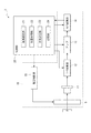
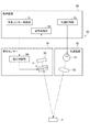
図1は、本発明に係る第1実施形態の分光測定装置の構成を示す概略図である。
分光測定装置1は、本発明の電子機器であり、測定対象Xで反射された測定対象光に基づいて、測定対象光のスペクトルを測定する装置である。なお、本実施形態では、測定対象Xで反射した測定対象光を測定する例を示すが、測定対象Xとして、例えば液晶パネル等の発光体を用いる場合、発光体から発光された光を測定対象光としてもよい。
この分光測定装置1は、図1に示すように、光学モジュール10と、制御部20と、を備えている。
(Configuration of spectrometer)
FIG. 1 is a schematic diagram showing the configuration of the spectrometer according to the first embodiment of the present invention.
The
As shown in FIG. 1, the
(光学モジュールの構成)
光学モジュール10は、波長可変干渉フィルター5と、ディテクター11と、I−V変換器12と、アンプ13と、A/D変換器14と、電圧制御部15とを備えて構成される。
(Configuration of optical module)
The
ディテクター11は、光学モジュール10の波長可変干渉フィルター5を透過した光を受光し、受光した光の光強度に応じた検出信号(電流)を出力する。
I−V変換器12は、ディテクター11から入力された検出信号を電圧値に変換し、アンプ13に出力する。
アンプ13は、I−V変換器12から入力された検出信号に応じた電圧(検出電圧)を増幅する。
A/D変換器14は、アンプ13から入力された検出電圧(アナログ信号)をデジタル信号に変換し、制御部20に出力する。
電圧制御部15は、波長可変干渉フィルター5の後述する駆動電極に電圧を印加する。そして、波長可変干渉フィルター5から印加電圧に応じた目的波長の光を透過させる。
The
The
The
The A /
The
(波長可変干渉フィルターの構成)
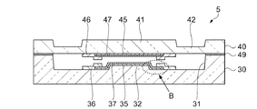
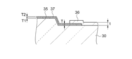
図2は本実施形態に係る波長可変干渉フィルターの平面図であり、図3は図2のA−A断線に沿う断面図である。図4は図3のB部拡大図である。
本実施形態の波長可変干渉フィルター5は、いわゆるファブリーペローエタロンである。この波長可変干渉フィルター5は、固定基板(第1基板)30と、可動基板(第2基板)40とを備えている。これらの固定基板30及び可動基板40は、それぞれ例えば石英ガラス、ソーダガラス、結晶性ガラス、鉛ガラス、カリウムガラス、ホウケイ酸ガラス、無アルカリガラスなどの各種ガラスや、水晶、シリコンなどにより形成されている。
そして、これらの固定基板30と可動基板40とは、例えばシロキサンを主成分とするプラズマ重合膜などにより構成された接合膜49により接合され、一体に構成されている。
(Configuration of wavelength variable interference filter)
2 is a plan view of the wavelength tunable interference filter according to the present embodiment, and FIG. 3 is a cross-sectional view taken along the line AA in FIG. FIG. 4 is an enlarged view of a portion B in FIG.
The variable
The fixed
固定基板30には、第1反射膜35が設けられ、可動基板40には、第2反射膜45が設けられており、これらの第1反射膜35および第2反射膜45は、反射膜間ギャップを介して対向配置されている。さらに、第1反射膜35の上に導電性の第1導電膜37が積層され、第2反射膜45の上に導電性の第2導電膜47が積層されている。これらの第1導電膜37、第2導電膜47は、それぞれ第1反射膜35、第2反射膜45と同じ大きさに形成されている。そして、波長可変干渉フィルター5には、この反射膜間ギャップのギャップ量を変更するのに用いられる静電アクチュエーターが設けられている。この静電アクチュエーターは、固定基板30に設けられた第1駆動電極36(第1接続電極)と、可動基板40に設けられた第2駆動電極46(第2接続電極)とにより構成されている。この一対の第1駆動電極36、第2駆動電極46は、電極間ギャップを介して対向し、静電アクチュエーターとして機能する。なお、電極間ギャップのギャップ量は反射膜間ギャップよりもギャップ量が大きくなる構成、または小さくなる構成のどちらであっても良い。
The fixed
第1駆動電極36はリング形状に形成されている。第1駆動電極36の構成については特に限定されないが、例えば下地層をCr膜とし、その上に電極層としてAu膜を積層した構成の電極を利用できる。この場合、Cr膜の厚み寸法は約10nm、Au膜の厚み寸法は100nm〜200nmに構成されている。なお、下地膜のCr膜に変えて、Ti,NiCr,TiWなどの膜を用いても良い。また、第1駆動電極36はITO(酸化インジウムスズ)などの透明導電膜を利用しても良い。
The
第1駆動電極36は、第1反射膜35の上に形成された第1導電膜37の外周縁の全周において接触している。第1反射膜35はAgまたはAgを主成分とする合金で形成され、第1反射膜35の厚み寸法は10nm〜80nmである。
第1反射膜35として、AgまたはAgを主成分とする合金を用いることで、光の透過特性、反射特性の両者に優れた特性を得ることができる。
第1導電膜37はインジウム系酸化物、スズ系酸化物、亜鉛系酸化物などの透明導電膜で形成されている。具体的にはITO、ICO(セリウムドープ酸化インジウム)、AZO(アルミドープ酸化亜鉛)、SnOなどが用いられる。また、DLC(ダイヤモンドライクカーボン)を利用することもできる。そして、第1導電膜37の厚み寸法は5nm〜30nmである。
このようにして、第1反射膜35の光透過特性を阻害することなく第1導電膜37を形成することができる。
The
By using Ag or an alloy containing Ag as a main component as the first
The first
In this way, the first
ここで、図4に示すように、第1反射膜35の厚み寸法T1と第1導電膜37の厚み寸法T2の和をT(T=T1+T2)、第1駆動電極36の厚み寸法をtとすると、T<tという関係にある。
このため、第1駆動電極36が第1導電膜37の上から覆っても固定基板30との段差が小さいため、第1駆動電極36が第1導電膜37の端部に形成でき断線することがない。
このように、第1反射膜35、第1導電膜37と第1駆動電極36とが電気的に接続され導通が図られている。
Here, as shown in FIG. 4, the sum of the thickness dimension T1 of the first
For this reason, even if the
In this manner, the first
また、この接続部において、第1駆動電極36と第1反射膜35と間に第1導電膜37が設けられていることで、第1反射膜35のAg原子が第1駆動電極36のCr膜、Au膜へ拡散するのを防止することができ、接続配線の断線を抑制することができる。
Further, in this connection portion, the first
第2駆動電極46も第1駆動電極36と同様にリング形状に形成され、第2駆動電極46の構成については特に限定されないが、例えば下地層をCr膜とし、その上に電極層としてAu膜を積層した構成の電極を利用できる。このCr膜、Au膜は、それぞれ第1駆動電極36と同様の厚み寸法で形成されている。
Similarly to the
第2駆動電極46は、第2反射膜45の上に形成された第2導電膜47の外周縁の全周において接触している。第2反射膜45は、第1反射膜35と同様にAgまたはAgを主成分とする合金で形成され、第2反射膜45の厚み寸法は10nm〜80nmである。
第2導電膜47はインジウム系酸化物、スズ系酸化物、亜鉛系酸化物などの透明導電膜で形成されている。具体的にはITO、ICO(セリウムドープ酸化インジウム)、AZO(アルミドープ酸化亜鉛)、SnOなどが用いられる。また、DLC(ダイヤモンドライクカーボン)を利用することもできる。そして、第2導電膜47の厚み寸法は5nm〜30nmである。
このようにして、第2反射膜45の光透過特性を阻害することなく第2導電膜47を形成することができる。
The
The second
In this way, the second
ここで、第2反射膜45の厚み寸法と第2導電膜47の厚み寸法の和は、第2駆動電極46の厚み寸法よりも小さい関係にある。
このため、第2駆動電極46が第2導電膜47の上から形成しても可動基板40との段差が小さいため、第2駆動電極46が第2導電膜47の端部に十分に形成でき断線することがない。
このように、第2反射膜45、第2導電膜47と第2駆動電極46とが電気的に接続され導通が図られている。
Here, the sum of the thickness dimension of the second
For this reason, even if the
In this way, the second
また、この接続部において、第2駆動電極46と第2反射膜45との間に第2導電膜47が設けられていることで、第2反射膜45のAg原子が第2駆動電極46のCr膜、Au膜へ拡散するのを防止することができ、接続配線の断線を抑制することができる。
In this connection portion, the second
上記の波長可変干渉フィルター5は、第1反射膜35と第1駆動電極36、第2反射膜45と第2駆動電極46が電気的に接続され、第1反射膜35、第2反射膜45に帯電する静電気を外部に逃がす構成となっている。
In the variable
(固定基板の構成)
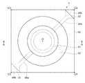
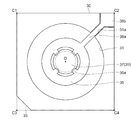
図5は、固定基板30を可動基板40側から見た平面図である。
固定基板30は、静電アクチュエーターによる静電引力や、固定基板30上に形成される膜部材の内部応力により、固定基板30に撓みが生じないように充分な厚みで形成されている。
この固定基板30は、図5に示すように、例えばエッチング等により形成された凹部31および第1反射膜35が配置される凸部32を備える。また、固定基板30の外周縁の一部(頂点C3)には、切欠部33が設けられており、この切欠部33から後述する可動基板40の電極パッド48bが波長可変干渉フィルター5の表面に露出される構成となる。
(Configuration of fixed substrate)
FIG. 5 is a plan view of the fixed
The fixed
As shown in FIG. 5, the fixed
凹部31は、固定基板30の厚み方向の平面視で、固定基板30のフィルター中心点Oを中心としたリング状に形成されている。凸部32は、固定基板30の厚み方向の平面視において、凹部31の中心部から可動基板40側に突出して形成されている。
この凹部31の底面は、静電アクチュエーターの第1駆動電極36が配置される電極設置面となる。また、凸部32の突出先端面は、第1反射膜35が配置される反射膜設置面となる。
The
The bottom surface of the
また、固定基板30には、凹部31から、固定基板30の頂点C2に向かって延出する電極引出溝31aが設けられている。そして、電極引出溝31aは凹部31と同じ深さに形成されている。
The fixed
凹部31の底面には、フィルター中心点Oを中心とした仮想円上に沿って設けられる第1駆動電極36が設けられている。第1駆動電極36は凸部32と同心円状に形成されている。
そして、固定基板30には、第1駆動電極36の外周縁から、頂点C2に向かう電極引出溝31aに沿って、頂点C2まで延出する引出電極38aが設けられている。この引出電極38aの先端部は、電圧制御部15に接続される電極パッド38bを構成する。
A
The fixed
第1駆動電極36、引出電極38a、電極パッド38bは、下地層をCr膜とし、その上に電極層としてAu膜を積層した構造を有している。
電極層としてAu膜を用いる場合、波長可変干渉フィルター5を電圧制御部15に接続する際の端子接続性が良好となり、また、導電性が良好であるため、電気抵抗の増大を抑えることができる。また、下地層として、Auとの密着性、及びガラス基板(固定基板30)との密着性が高いCr膜を用いることで、第1駆動電極36、引出電極38a、電極パッド38bの剥離を防止できる。
なお、本実施形態では、下地層をCr膜、電極層をAu膜とした2層構成の電極を例示したが、ガラス基板に対して密着性があり、かつ導電性を有する他の金属膜(Alなど)を単層で用いてもよい。
The
When an Au film is used as the electrode layer, the terminal connectivity when connecting the wavelength
In the present embodiment, an electrode having a two-layer structure in which the base layer is a Cr film and the electrode layer is an Au film is exemplified, but other metal films having adhesion to a glass substrate and having conductivity ( Al) may be used in a single layer.
また、第1駆動電極36上に、第1駆動電極36及び第2駆動電極46の間の絶縁性を確保するための絶縁膜が積層される構成としてもよい。
なお、本実施形態では、凹部31の底面に1つの第1駆動電極36が設けられる構成を示すが、例えば、フィルター中心点Oを中心とした同心円となる2つの電極が設けられる構成(二重電極構成)などとしてもよい。
In addition, an insulating film for ensuring insulation between the
In the present embodiment, a configuration in which one
凸部32は、凹部31と同軸上で略円柱状に形成され、可動基板40に対面する反射膜設置面を備えている。
この反射膜設置面から凹部31の底面に延出して第1反射膜35が設置されている。この第1反射膜35の上に第1導電膜37が形成されている。
そして、第1駆動電極36が第1反射膜35の上に形成された第1導電膜37の外周の外縁部の全周において接続され、第1反射膜35、第1導電膜37と第1駆動電極36とが電気的に接続されて導通が図られている。このように、第1駆動電極36は第1導電膜37の外縁部の全周において接触していることから、配線の接続における電気抵抗を下げることができ、良好な接続をすることができる。
The
A first
The
(可動基板の構成)
図6は、可動基板40を固定基板30側から見た平面図である。なお、図6における可動基板40の各頂点C1,C2,C3,C4は、図5に示す固定基板30の各頂点C1,C2,C3,C4に対応する。
可動基板40は、図3及び図6に示すように、可動基板40の厚み方向の平面視で、フィルター中心点Oを中心とした円形状の可動部41と、可動部41と同軸であり可動部41を保持する保持部42と、を備えている。
また、可動基板40には、図6に示すように、頂点C2に切欠部43が設けられ、上述したように、この切欠部43から固定基板30の電極パッド38bが露出する。
(Configuration of movable substrate)
FIG. 6 is a plan view of the
As shown in FIGS. 3 and 6, the
Further, as shown in FIG. 6, the
可動部41は、保持部42よりも厚み寸法が大きく形成されている。この可動部41は、可動基板40の厚み方向の平面視において、少なくとも反射膜設置面の外周縁の径寸法よりも大きい径寸法に形成されている。そして、この可動部41の固定基板30に対向する面には、第2反射膜45、第2導電膜47及び第2駆動電極46が設けられている。
なお、可動部41の固定基板30と対向する面とは反対側の面には、反射防止膜が形成されていてもよい。
The
Note that an antireflection film may be formed on the surface of the
第2駆動電極46は、図6に示すように、可動基板40の厚み方向の平面視において、第2反射膜45の外側で、第1駆動電極36に対向する領域に設けられている。
そして、第2駆動電極46には、頂点C3方向に延出する引出電極48aが設けられている。この引出電極48aの先端部は、電圧制御部15に接続される電極パッド48bを構成する。
上述したような電極構成では、図3に示すように、第1駆動電極36及び第2駆動電極46が重なる円弧領域により、静電アクチュエーターが構成されている。
As shown in FIG. 6, the
The
In the electrode configuration as described above, as shown in FIG. 3, the electrostatic actuator is configured by an arc region where the
第2駆動電極46、引出電極48a、電極パッド48bは、下地層をCr膜とし、その上に電極層としてAu膜を積層した構造を有している。
電極層としてAu膜を用いる場合、波長可変干渉フィルター5を電圧制御部15に接続する際の端子接続性が良好となり、また、導電性が良好であるため、電気抵抗の増大を抑えることができる。また、下地層として、Auとの密着性、及びガラス基板(可動基板40)との密着性が高いCrを用いることで、第2駆動電極46、引出電極48a、電極パッド48bの剥離を防止できる。
なお、本実施形態では、下地層をCr膜、電極層をAu膜とした2層構成の電極を例示したが、ガラス基板に対して密着性があり、かつ導電性を有する他の金属膜(Alなど)を単層で用いてもよい。
The
When an Au film is used as the electrode layer, the terminal connectivity when connecting the wavelength
In the present embodiment, an electrode having a two-layer structure in which the base layer is a Cr film and the electrode layer is an Au film is exemplified, but other metal films having adhesion to a glass substrate and having conductivity ( Al) may be used in a single layer.
また、第2駆動電極46上に、第1駆動電極36及び第2駆動電極46の間の絶縁性を確保するための絶縁膜が積層される構成としてもよい。
なお、本実施形態では、1つの第2駆動電極46が設けられる構成を示すが、例えば、フィルター中心点Oを中心とした同心円となる2つの電極が設けられる構成(二重電極構成)としてもよい。
In addition, an insulating film for ensuring insulation between the
In the present embodiment, a configuration in which one
第2反射膜45は、第1反射膜35と同様の材料により構成される。この第2反射膜45の上に第2導電膜47が形成されている。
そして、第2駆動電極46が第2反射膜45の上に形成された第2導電膜47の外周の外縁部の全周において接続され、第2反射膜45、第2導電膜47と第2駆動電極46とが電気的に接続されて導通が図られている。このように、第2駆動電極46は第2導電膜47の外縁部の全周において接触していることから、配線の接続における電気抵抗を下げることができ、良好な接続をすることができる。
The second
The
保持部42は、可動部41の周囲を囲うダイヤフラムであり、可動部41よりも厚み寸法が小さく形成されている。このような保持部42は、可動部41よりも撓みやすく、僅かな静電引力により変位し、可動部41を固定基板30側に進退可能に保持する。この際、可動部41が保持部42よりも厚み寸法が大きく、剛性が大きくなるため、保持部42が静電引力により固定基板30側に引っ張られた場合でも、可動部41の形状変化が抑制される。したがって、可動部41に設けられた第2反射膜45の撓みも抑制され、第1反射膜35及び第2反射膜45を平行状態に維持することが可能となる。
なお、本実施形態では、ダイヤフラムの保持部42を例示するが、これに限定されず、例えば、フィルター中心点Oを中心として、等角度間隔で配置された梁状の保持部が設けられる構成などとしてもよい。
The holding
In the present embodiment, the
(電圧制御部の構成)
図1に戻り、電圧制御部15は、上述の波長可変干渉フィルター5の電極パッド38b、48bに接続されている。
そして、電圧制御部15は、制御部20から測定対象波長に対応した電圧指令信号を受信すると、対応する電圧を電極パッド38b、48b間に印加する。これにより、波長可変干渉フィルター5の静電アクチュエーター(第1駆動電極36及び第2駆動電極46間)に、印加電圧に基づいた静電引力が発生し、可動部41が固定基板30側に変位して、反射膜間ギャップのギャップ量が変化する。
(Configuration of voltage controller)
Returning to FIG. 1, the
And the
(制御部の構成)
制御部20は、例えばCPUやメモリー等が組み合わされることで構成され、分光測定装置1の全体動作を制御する。この制御部20は、図1に示すように、波長設定部21と、光量取得部22と、分光測定部23と、を備える。
また、制御部20は、各種データを記憶する記憶部24を備え、記憶部24には、静電アクチュエーターを制御するためのV−λ(電圧−波長)データが記憶される。
このV−λデータは、静電アクチュエーターに印加する電圧(V)に対する、波長可変干渉フィルター5を透過する光のピーク波長(λ)の関係を示すデータである。
(Configuration of control unit)
The
The
This V-λ data is data indicating the relationship between the voltage (V) applied to the electrostatic actuator and the peak wavelength (λ) of the light transmitted through the wavelength
波長設定部21は、波長可変干渉フィルター5により取り出す光の目的波長を設定するとともに、記憶部24に記憶されたV−λデータから設定した目的波長に対応する目標電圧値を読み込む。そして、波長設定部21は、読み込んだ目標電圧値を印加させる旨の制御信号を電圧制御部15に出力する。これにより、電圧制御部15から静電アクチュエーターに目標電圧値の電圧が印加される。
光量取得部22は、ディテクター11により取得された光量に基づいて、波長可変干渉フィルター5を透過した目的波長の光の光量を取得する。
分光測定部23は、光量取得部22により取得された光量に基づいて、測定対象光のスペクトル特性を測定する。
The
The light quantity acquisition unit 22 acquires the light quantity of the target wavelength light transmitted through the wavelength
The
分光測定部23における分光測定方法としては、例えば、測定対象波長に対してディテクター11により検出された光量を、測定対象波長の光量として分光スペクトルを測定する方法や、複数の測定対象波長の光量に基づいて分光スペクトルを推定する方法等が挙げられる。
分光スペクトルを推定する方法としては、例えば、複数の測定対象波長に対する光量のそれぞれを行列要素とした計測スペクトル行列を生成し、この計測スペクトル行列に対して、所定の変換行列を作用させることで、測定対象となる光の分光スペクトルを推定する。この場合、分光スペクトルが既知である複数のサンプル光を、分光測定装置1により測定し、測定により得られた光量に基づいて生成される計測スペクトル行列に変換行列を作用させた行列と、既知の分光スペクトルとの偏差が最小となるように、変換行列を設定する。
As a spectroscopic measurement method in the
As a method of estimating a spectral spectrum, for example, by generating a measurement spectrum matrix having matrix elements as light amounts for a plurality of measurement target wavelengths, a predetermined conversion matrix is applied to this measurement spectrum matrix, Estimate the spectrum of the light to be measured. In this case, a plurality of sample lights whose spectral spectra are known are measured by the
[波長可変干渉フィルターの製造方法]
次に、上述した波長可変干渉フィルター5の製造方法について、図面に基づいて説明する。波長可変干渉フィルター5の製造は、固定基板の製造工程、可動基板の製造工程、基板の接合工程から成り立っている。
[Manufacturing method of tunable interference filter]
Next, the manufacturing method of the wavelength
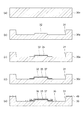
(固定基板の製造工程)
図7は、固定基板の製造工程を示す説明図である。
まず、図7(a)に示すように、固定基板30の材料である石英ガラス基板などで形成された第1基材30aを用意し、第1基材30aの両面を、表面粗さRaが1nm以下となるまで精密研磨する。
(Fixed substrate manufacturing process)
FIG. 7 is an explanatory view showing a manufacturing process of the fixed substrate.
First, as shown in FIG. 7A, a
次に、そして、図7(b)に示すように、第1基材30aの基板表面をエッチングにより加工する。
具体的には、第1基材30aの基板表面にレジストを塗布して、塗布されたレジストをフォトリソグラフィ法により露光・現像することで、凹部31と凸部32を形成するための開口部をパターニングする。
そして、第1基材30aの両面に対して、例えばフッ酸系溶液を用いたウェットエッチングを施す。この時、凸部32の上面までの深さのエッチングを行う。この後、凹部31の所定の深さまでエッチングするための開口部をレジストでパターニングし、ウェットエッチングを実施する。
これにより、図7(b)に示すように、固定基板30の外形状が決定された第1基材30aが形成される。
Next, as shown in FIG. 7B, the substrate surface of the
Specifically, a resist is applied to the substrate surface of the
Then, wet etching using, for example, a hydrofluoric acid solution is performed on both surfaces of the
Thereby, as shown in FIG. 7B, the
次に、図7(c)に示すように、凸部32の上面から凹部31の底面に延出する第1反射膜35を形成する。
本実施形態では、第1反射膜35として、Ag膜またはAg合金膜を用いる。第1反射膜35として、Ag膜やAg合金膜を用いる場合、第1基材30aの凹部31に、真空蒸着法やスパッタリング法により第1反射膜35の膜層を形成する。この後、フォトリソグラフィ法を用いて第1反射膜35の形状を形成する。Ag膜またはAg合金膜のエッチングには、リン硝酢酸水溶液が用いられる。
Next, as shown in FIG. 7C, a first
In the present embodiment, an Ag film or an Ag alloy film is used as the first
そして、図7(d)に示すように、第1反射膜35の上に第1導電膜37を形成する。この第1導電膜37は第1反射膜35と同じ形状に形成される。
本実施形態では、第1導電膜37としてITO膜を用いる。第1基材30aの凹部31にスパッタリング法により第1導電膜37の膜層を形成する。この後、フォトリソグラフィ法を用いて第1導電膜37の形状を形成する。なお、ITO膜のエッチングには、酸性の溶液が用いられる。
Then, as shown in FIG. 7D, a first
In the present embodiment, an ITO film is used as the first
次に、第1基材30aの凹部31に第1導電膜37の上から、第1駆動電極36、引出電極38a、電極パッド38bを形成する電極材料を、蒸着法やスパッタリング法等を用いて成膜する。ここでは、下地層としてCr膜を成膜した後、電極層としてAu膜を成膜する。そして、フォトリソグラフィ法を用いてパターニングすることで、図7(e)に示すように、第1駆動電極36、引出電極38a、電極パッド38bを形成する。
Au膜のエッチングにおいては、ヨウ素とヨウ化カリウムの混合液が用いられ、Cr膜のエッチングには硝酸セリウムアンモニウム水溶液が用いられる。
なお、図7(e)において、引出電極38a、電極パッド38bの図示は省略している。
ここで、第1駆動電極36の厚み寸法は、第1反射膜35の厚み寸法よりも大きいため、第1反射膜35による固定基板30との段差をカバーして、この段差の部分での断線を防止することができる。
また、第1反射膜35の上に第1導電膜37が形成されているため、第1駆動電極36を形成する工程における薬液などによる第1反射膜35の損傷を防止することができる。
Next, an electrode material for forming the
In etching the Au film, a mixed solution of iodine and potassium iodide is used, and a cerium ammonium nitrate aqueous solution is used in etching the Cr film.
In FIG. 7E, the drawing
Here, since the thickness dimension of the
In addition, since the first
さらに、第1基材30aの上面(可動基板40と接する面)にシロキサンを主成分とするプラズマ重合膜などにより構成された接合膜49を形成する。接合膜49は、例えばプラズマCVD法等により成膜する。接合膜49の厚みとしては、例えば10nm〜1000nmとすればよい。
このようにして、固定基板30が製造される。
Further, a
In this way, the fixed
(可動基板の製造工程)
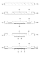
次に、可動基板の製造工程について説明する。図8は、可動基板の製造工程を示す説明である。
まず、図8(a)に示すように、可動基板40の材料である石英ガラス基板などで形成された第2基材40aを用意し、第2基材40aの両面を、表面粗さRaが1nm以下となるまで精密研磨する。
そして、第2基材40aの全面にレジストを塗布し、塗布されたレジストをフォトリソグラフィ法により露光・現像して、保持部42が形成される箇所をパターニングする。
次に、第1基材30aと同様にフッ酸系溶液を用いて、第2基材40aをウェットエッチングすることで、図8(b)に示すように、可動部41、保持部42を形成する。これにより、可動基板40の基板形状が決定された第2基材40aが製造される。
(Movable substrate manufacturing process)
Next, the manufacturing process of the movable substrate will be described. FIG. 8 is a diagram illustrating a manufacturing process of the movable substrate.
First, as shown in FIG. 8A, a
And a resist is apply | coated to the whole surface of the
Next, as shown in FIG. 8B, the
次に、図8(c)に示すように、第2基材40aの可動部41、保持部42を形成した面とは反対の面の中央部に第2反射膜45を形成する。
本実施形態では、第2反射膜45として、Ag膜またはAg合金膜を用いる。第2反射膜45として、Ag膜やAg合金膜を用いる場合、真空蒸着法やスパッタリング法により第2反射膜45の膜層を形成する。この後、フォトリソグラフィ法を用いて第2反射膜45の形状を形成する。Ag膜またはAg合金膜のエッチングには、リン硝酢酸水溶液が用いられる。
Next, as shown in FIG. 8C, a second
In the present embodiment, an Ag film or an Ag alloy film is used as the second
そして、図8(d)に示すように、第2反射膜45の上に第2導電膜47を形成する。この第2導電膜47は第2反射膜45と同じ形状に形成される。
本実施形態では、第2導電膜47としてITO膜を用いる。第2基材40aにスパッタリング法により第2導電膜47の膜層を形成する。この後、フォトリソグラフィ法を用いて第2導電膜47の形状を形成する。なお、ITO膜のエッチングには、酸性の溶液が用いられる。
Then, as shown in FIG. 8D, a second
In the present embodiment, an ITO film is used as the second
次に、第2基材40aに第2導電膜47の上から、第2駆動電極46、引出電極48a、電極パッド48bを形成する電極材料を、蒸着法やスパッタリング法等を用いて成膜する。ここでは、下地層としてCr膜を成膜した後、電極層としてAu膜を成膜する。そして、フォトリソグラフィ法を用いてパターニングすることで、図8(e)に示すように、第2駆動電極46、引出電極48a、電極パッド48bを形成する。
Au膜のエッチングにおいては、ヨウ素とヨウ化カリウムの混合液が用いられ、Cr膜のエッチングには硝酸セリウムアンモニウム水溶液が用いられる。
なお、図8(e)において、引出電極48a、電極パッド48bの図示は省略している。
ここで、第2駆動電極46の厚み寸法は、第2反射膜45の厚み寸法よりも大きいため、第2反射膜45による可動基板40との段差をカバーして、この段差の部分での断線を防止することができる。
また、第2反射膜45の上に第2導電膜47が形成されているため、第2駆動電極46を形成する工程における薬液などによる第2反射膜45の損傷を防止することができる。
Next, an electrode material for forming the
In etching the Au film, a mixed solution of iodine and potassium iodide is used, and a cerium ammonium nitrate aqueous solution is used in etching the Cr film.
In FIG. 8E, the drawing
Here, since the thickness dimension of the
In addition, since the second
さらに、第2基材40aの上面(固定基板30と接する面)にシロキサンを主成分とするプラズマ重合膜などにより構成された接合膜49を形成する。接合膜49は、例えばプラズマCVD法等により成膜する。接合膜49の厚みとしては、例えば10nm〜1000nmとすればよい。
このようにして、可動基板40が製造される。
Further, a
In this way, the
(基板の接合工程)
次に、基板の接合工程について説明する。図9は、固定基板と可動基板との接合工程を示す説明図である。
まず、固定基板30と可動基板40の接合膜49に対して活性化エネルギーを付与するために、O2プラズマ処理、N2プラズマ処理またはUV処理を行う。
プラズマ重合膜に活性化エネルギーを付与した後、これらの固定基板30と可動基板40のアライメント調整を行い、接合膜49を介して固定基板30と可動基板40を重ね合わせ、接合部分に荷重をかける。これにより、固定基板30と可動基板40が接合される。
このような工程を経て、波長可変干渉フィルター5が製造される。
(Board bonding process)
Next, the substrate bonding process will be described. FIG. 9 is an explanatory diagram illustrating a bonding process between the fixed substrate and the movable substrate.
First, in order to apply activation energy to the
After applying activation energy to the plasma polymerization film, alignment adjustment of the fixed
The wavelength
(第1実施形態の作用効果)
以上、本実施形態に係る波長可変干渉フィルター5は、第1反射膜35を覆う第1導電膜37が形成され、第1反射膜35と第1導電膜37との厚み寸法の和よりも厚み寸法の大きい第1駆動電極36が第1導電膜37の上から形成されている。
このように、第1駆動電極36の厚み寸法は、第1反射膜35の厚み寸法よりも大きいため、第1反射膜35による固定基板30との段差をカバーして、この段差の部分での断線を防止することができる。
また、第2反射膜45を覆う第2導電膜47が形成され、第2反射膜45と第2導電膜47との厚み寸法の和よりも厚み寸法の大きい第2駆動電極46が第2導電膜47の上から形成されている。
このように、第2駆動電極46の厚み寸法は、第2反射膜45の厚み寸法よりも大きいため、第2反射膜45による可動基板40との段差をカバーして、この段差の部分での断線を防止することができる。
さらに、第1導電膜37、第2導電膜47を設けることで第1反射膜35、第2反射膜45のAg原子が第1駆動電極36、第2駆動電極46のCr膜、Au膜への拡散を防止することができ、配線の断線を抑制することができる。
このことから、第1反射膜35と第1駆動電極36との導通及び、第2反射膜45と第2駆動電極46との導通を確実にし、配線の接続信頼性を向上することができる。
(Operational effects of the first embodiment)
As described above, in the wavelength
As described above, since the thickness dimension of the
A second
Thus, since the thickness dimension of the
Further, by providing the first
Thus, the conduction between the first
また、第1導電膜37及び第2導電膜47の材料はインジウム系酸化物、スズ系酸化物、亜鉛系酸化物及びこれらの混合物から選択される材料である。
第1導電膜37及び第2導電膜47として、これらの材料を用いることで、第1反射膜35、第2反射膜45から第1駆動電極36、第2駆動電極46への拡散を効果的に防止できる。また、これらの材料を用いることで製造工程における薬液から第1反射膜35、第2反射膜45を保護することができる。
The material of the first
By using these materials as the first
また、本実施形態に係る光学モジュール10は、上記の配線の接続信頼性を向上する波長可変干渉フィルター5を備えているため、光学モジュール10の信頼性を向上させることができる。
In addition, since the
さらに、電子機器としての分光測定装置1は、上記の配線の接続信頼性を向上する波長可変干渉フィルター5を備えているため、分光測定装置1の信頼性を向上させることができる。
Furthermore, since the
(駆動電極と導電膜の接続状態の変形例)
次に、波長可変干渉フィルター5における、駆動電極(第1駆動電極、第2駆動電極)と反射膜(第1反射膜、第2反射膜)の上に設けられた導電膜(第1導電膜、第2導電膜)の接続状態の変形例について説明する。固定基板30と可動基板40にそれぞれ駆動電極と反射膜、導電膜を有するが、ここでは、固定基板30側について説明する。そして、第1実施形態と同様な構成については、同符号を付し説明を省略する。
(Modification of connection state between drive electrode and conductive film)
Next, the conductive film (first conductive film) provided on the drive electrode (first drive electrode, second drive electrode) and the reflective film (first reflective film, second reflective film) in the variable
図10は第1実施形態における第1駆動電極の形状の変形例を示す平面図である。
本変形例では第1実施形態と第1駆動電極の形状が異なる。
固定基板30に形成された第1駆動電極36は、リング状の内周縁から延出する複数の延出部36aが形成され、このそれぞれの延出部36aが第1導電膜37と接触している。
このように、上記の形状の第1駆動電極36を用いて、第1導電膜37との導通をとっても良く、第1実施形態と同様の効果を奏することができる。
FIG. 10 is a plan view showing a modification of the shape of the first drive electrode in the first embodiment.
In this modification, the shape of the first embodiment is different from that of the first embodiment.
The
As described above, the
図11は第1実施形態における第1駆動電極と第1導電膜との接触状態の変形例を示す固定基板の断面図である。
図11(a)に示すように、第1反射膜35および第1導電膜37は固定基板30の中央から凹部31の底面にかけて円形状に形成されている。そして、第1導電膜37の外周部に沿ってリング状の第1駆動電極36が、第1導電膜37の上に載った状態で形成されている。このように、第1駆動電極36と第1導電膜37との接触面積を大きくすることで配線の接続における電気抵抗を下げることができ、良好な接続をすることができる。
FIG. 11 is a cross-sectional view of the fixed substrate showing a modification of the contact state between the first drive electrode and the first conductive film in the first embodiment.
As shown in FIG. 11A, the first
また、図11(b)に示すように、固定基板30の中央に設けられた第1反射膜35よりも大きい面積で第1反射膜35と重なる第1導電膜37が形成されている。そして、平面視で第1反射膜35と重ならない第1導電膜37の外縁部にて第1駆動電極36と接触している。このように、第1反射膜35の外縁部の側面まで第1導電膜37が形成できることになり、第1駆動電極36の製造工程において薬液が第1反射膜35と触れる部分がなくなり、第1反射膜35に損傷を与えることがない。
In addition, as shown in FIG. 11B, a first
なお、上記の実施形態および変形例では、固定基板30と可動基板40との両者に同じ構成の駆動電極と反射膜を有する例を説明したが、両者が同じ構造でなくても良く、第1実施形態、変形例で説明した構造を組み合わせて実施しても良い。
また、第1反射膜と接続する第1接続電極として第1駆動電極、第2反射膜と接続する第2接続電極として第2駆動電極、を説明したが、この例に限らず、反射膜と接続する接続電極として、静電容量を測定するモニター電極などと接続する構成であっても良い。
[第2実施形態]
In the embodiment and the modification described above, the example in which both the fixed
Further, the first drive electrode is described as the first connection electrode connected to the first reflective film, and the second drive electrode is described as the second connection electrode connected to the second reflective film. However, the present invention is not limited to this example. The connection electrode may be connected to a monitor electrode for measuring the capacitance.
[Second Embodiment]
次に、本発明の第2実施形態について、図面に基づいて説明する。
上記第1実施形態の分光測定装置1では、光学モジュール10に対して、波長可変干渉フィルター5が直接設けられる構成とした。しかしながら、光学モジュールとしては、複雑な構成を有するものもあり、特に小型化された光学モジュールに対して、波長可変干渉フィルター5を直接設けることが困難な場合がある。本実施形態では、そのような光学モジュールに対しても、波長可変干渉フィルター5を容易に設置可能にする光学フィルターデバイスについて、以下に説明する。
図12は、本発明に係る第2実施形態の光学フィルターデバイスの概略構成を示す断面図である。
Next, 2nd Embodiment of this invention is described based on drawing.
In the
FIG. 12 is a cross-sectional view showing a schematic configuration of the optical filter device according to the second embodiment of the present invention.
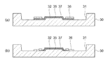
図12に示すように、光学フィルターデバイス60は、波長可変干渉フィルター5と、波長可変干渉フィルター5を収納する筐体61と、を備えている。
筐体61は、ベース基板62と、リッド70と、ベース側ガラス基板75と、リッド側ガラス基板76と、を備える。
As shown in FIG. 12, the
The
ベース基板62は、例えば単層セラミック基板により構成される。このベース基板62には、波長可変干渉フィルター5の可動基板40が設置される。ベース基板62への可動基板40の設置としては、例えば接着層等を介して配置されるものであってもよく、他の固定部材等に嵌合等されることで配置されるものであってもよい。また、ベース基板62には、光通過孔63が開口形成される。そして、この光通過孔63を覆うように、ベース側ガラス基板75が接合される。ベース側ガラス基板75の接合方法としては、例えば、ガラス原料を高温で熔解し、急冷したガラスのかけらであるガラスフリットを用いたガラスフリット接合、エポキシ樹脂等による接着などを利用できる。
The
このベース基板62のリッド70に対向するベース内側面64には、波長可変干渉フィルター5の各電極パッドに対応して内側端子部67が設けられている。なお、各電極パッドと内側端子部67との接続は、例えばFPC67aを用いることができ、例えばAgペースト、ACF(Anisotropic Conductive Film)、ACP(Anisotropic Conductive Paste)等により接合する。また、FPC67aによる接続に限られず、例えばワイヤーボンディング等による配線接続を実施してもよい。
また、ベース基板62は、各内側端子部67が設けられる位置に対応して、貫通孔66が形成されており、各内側端子部67は、貫通孔66に充填された導電性部材を介して、ベース基板62のベース内側面64とは反対側のベース外側面65に設けられた外側端子部68に接続されている。
そして、ベース基板62の外周部には、リッド70に接合されるベース接合部69が設けられている。
On the base
In addition, the
A base joint 69 that is joined to the
リッド70は、図12に示すように、ベース基板62のベース接合部69に接合されるリッド接合部72と、リッド接合部72から連続し、ベース基板62から離れる方向に立ち上がる側壁部73と、側壁部73から連続し、波長可変干渉フィルター5の固定基板30側を覆う天面部74とを備えている。このリッド70は、例えばコバール等の合金または金属により形成することができる。
このリッド70は、リッド接合部72と、ベース基板62のベース接合部69とが、接合されることで、ベース基板62に密着接合されている。
この接合方法としては、例えば、レーザー溶着の他、銀ロウ等を用いた半田付け、共晶合金層を用いた封着、低融点ガラスを用いた溶着、ガラス付着、ガラスフリット接合、エポキシ樹脂による接着等が挙げられる。これらの接合方法は、ベース基板62及びリッド70の素材や、接合環境等により、適宜選択することができる。
As shown in FIG. 12, the
The
As this joining method, for example, in addition to laser welding, soldering using silver brazing, sealing using a eutectic alloy layer, welding using low melting glass, glass adhesion, glass frit bonding, epoxy resin Adhesion etc. are mentioned. These bonding methods can be appropriately selected depending on the materials of the
リッド70の天面部74は、ベース基板62に対して平行となる。この天面部74には、光通過孔71が開口形成されている。そして、この光通過孔71を覆うように、リッド側ガラス基板76が接合される。リッド側ガラス基板76の接合方法としては、ベース側ガラス基板75の接合と同様に、例えばガラスフリット接合や、エポキシ樹脂等による接着などを用いることができる。
The
上述したような本実施形態の光学フィルターデバイス60では、筐体61により波長可変干渉フィルター5が保護されているため、外的要因による波長可変干渉フィルター5の破損を防止できる。
[第3実施形態]
In the
[Third Embodiment]
次に、上記第1実施形態で説明した波長可変干渉フィルターを使用した、電子機器について説明する。第3実施形態では、測定物の色度を測定する測色装置を例にとって説明する。
図13は測色装置の構成を示す概略図である。
測色装置80は、検査対象Aに光を照射する光源装置82と、測色センサー84(光学モジュール)と、測色装置80の全体動作を制御する制御装置86とを備える。
この測色装置80は、検査対象Aに光源装置82から光を照射し、検査対象Aから反射された検査対象光を測色センサー84にて受光し、測色センサー84から出力される検出信号に基づいて、検査対象光の色度を分析して測定する装置である。
Next, an electronic apparatus using the variable wavelength interference filter described in the first embodiment will be described. In the third embodiment, a color measurement device that measures the chromaticity of a measurement object will be described as an example.
FIG. 13 is a schematic diagram showing the configuration of the color measuring device.
The
The
光源装置82は、光源91、複数のレンズ92(図13には1つのみ図示)を備え、検査対象Aに対して白色光を射出する。また、複数のレンズ92には、コリメーターレンズが含まれてもよく、この場合、光源装置82は、光源91から射出された光をコリメーターレンズにより平行光とし、図示しない投射レンズから検査対象Aに向かって射出する。
なお、本実施形態では、光源装置82を備える測色装置80を例示するが、例えば検査対象Aが発光部材である場合、光源装置82を設けずに測色装置を構成してもよい。
The
In the present embodiment, the
光学モジュールとしての測色センサー84は、波長可変干渉フィルター5と、静電アクチュエーターに印加する電圧を制御し、波長可変干渉フィルター5で透過させる光の波長を変える電圧制御部94と、波長可変干渉フィルター5を透過した光を受光する受光部93(検出部)と、を備える。
また、測色センサー84は、検査対象Aで反射された反射光(検査対象光)を、波長可変干渉フィルター5に導光する光学レンズ(図示せず)を備えている。そして、この測色センサー84は、光学レンズに入射した検査対象光を波長可変干渉フィルター5で所定波長帯域の光に分光し、分光した光が受光部93にて受光される。
受光部93は、検出部としてフォトダイオードなどの光電変換素子により構成されており、受光量に応じた電気信号を生成する。そして、受光部93は制御装置86に接続され、生成した電気信号を受光信号として制御装置86に出力する。
The
The
The
電圧制御部94は、制御装置86からの入力される制御信号に基づいて、静電アクチュエーターに印加する電圧を制御する。
The
制御装置86は、測色装置80の全体動作を制御する。この制御装置86としては、例えば汎用パーソナルコンピューター、携帯情報端末、その他、測色専用コンピューターなどを用いることができる。
そして、制御装置86は、光源制御部95、測色センサー制御部97、および測色処理部96(分析処理部)などを備えて構成されている。
The
The
光源制御部95は、光源装置82に接続されている。そして、光源制御部95は、例えば利用者の設定入力に基づいて、光源装置82に所定の制御信号を出力し、光源装置82から所定の明るさの白色光を射出させる。
測色センサー制御部97は、測色センサー84に接続されている。そして、測色センサー制御部97は、例えば利用者の設定入力に基づいて、測色センサー84にて受光させる光の波長を設定し、この波長の受光量を検出する旨の制御信号を測色センサー84に出力する。これにより、測色センサー84の電圧制御部94は、制御信号に基づいて、利用者が所望する光の波長を透過させるよう、静電アクチュエーターへの印加電圧を設定する。
The light
The colorimetric
測色処理部96は、測色センサー制御部97を制御して、波長可変干渉フィルター5の反射膜間のギャップ寸法を変動させて、波長可変干渉フィルター5を透過する光の波長を変化させる。また、測色処理部96は、受光部93から入力される受光信号に基づいて、波長可変干渉フィルター5を透過した光量を取得する。そして、測色処理部96は、上記により得られた各波長の受光量に基づいて、検査対象Aから反射された光の色度を算出する。
The
このように、本実施形態の電子機器としての測色装置80および光学モジュールとしての測色センサー84は、配線の接続信頼性を向上する波長可変干渉フィルター5を備えているため、測色センサー84の信頼性を向上させることができる。
以上、第3実施形態では、電子機器として測色装置80を例示したが、その他、様々な分野に波長可変干渉フィルター、光学モジュール、電子機器を用いることができる。
例えば、特定物質の存在を検出するための光ベースのシステムとして用いることができる。このようなシステムとしては、例えば、波長可変干渉フィルターを用いた分光計測方式を採用して特定ガスを高感度検出する車載用ガス漏れ検出器や、呼気検査用の光音響希ガス検出器などのガス検出装置を例示できる。
[第4実施形態]
As described above, the
As described above, in the third embodiment, the
For example, it can be used as a light-based system for detecting the presence of a specific substance. As such a system, for example, an in-vehicle gas leak detector that detects a specific gas with high sensitivity by adopting a spectroscopic measurement method using a wavelength variable interference filter, a photoacoustic rare gas detector for a breath test, etc. A gas detection apparatus can be illustrated.
[Fourth Embodiment]
以下、ガス検出装置の一例を以下に図面に基づいて説明する。 Hereinafter, an example of the gas detection device will be described with reference to the drawings.
図14は、波長可変干渉フィルターを備えたガス検出装置の一例を示す概略図である。
図15は、ガス検出装置の制御系の構成を示すブロック図である。
このガス検出装置100は、図14に示すように、センサーチップ110と、吸引口120A、吸引流路120B、排出流路120C、および排出口120Dを備えた流路120と、本体部130と、を備えて構成されている。
本体部130は、流路120を着脱可能な開口を有するセンサー部カバー131、排出手段133、筐体134、光学部135、フィルター136、波長可変干渉フィルター5、および受光素子137(受光部)等を含む検出部(光学モジュール)と、検出された信号を処理し、検出部を制御する制御部138、電力を供給する電力供給部139等から構成されている。また、光学部135は、光を射出する光源135Aと、光源135Aから入射された光をセンサーチップ110側に反射し、センサーチップ側から入射された光を受光素子137側に透過するビームスプリッター135Bと、レンズ135C,135D,135Eと、により構成されている。
FIG. 14 is a schematic diagram illustrating an example of a gas detection device including a wavelength variable interference filter.
FIG. 15 is a block diagram illustrating a configuration of a control system of the gas detection device.
As shown in FIG. 14, the
The
また、図15に示すように、ガス検出装置100には、操作パネル140、表示部141、外部とのインターフェイスのための接続部142、電力供給部139が設けられている。電力供給部139が二次電池の場合には、充電のための接続部143を備えてもよい。
さらに、ガス検出装置100の制御部138は、CPU等により構成された信号処理部144、光源135Aを制御するための光源ドライバー回路145、波長可変干渉フィルター5を制御するための電圧制御部146、受光素子137からの信号を受信する受光回路147、センサーチップ110のコードを読み取り、センサーチップ110の有無を検出するセンサーチップ検出器148からの信号を受信するセンサーチップ検出回路149、および排出手段133を制御する排出ドライバー回路150などを備えている。
Further, as shown in FIG. 15, the
Further, the
次に、ガス検出装置100の動作について、以下に説明する。
本体部130の上部のセンサー部カバー131の内部には、センサーチップ検出器148が設けられており、このセンサーチップ検出器148でセンサーチップ110の有無が検出される。信号処理部144は、センサーチップ検出器148からの検出信号を検出すると、センサーチップ110が装着された状態であると判断し、表示部141へ検出動作を実施可能な旨を表示させる表示信号を出す。
Next, operation | movement of the
A
そして、例えば利用者により操作パネル140が操作され、操作パネル140から検出処理を開始する旨の指示信号が信号処理部144へ出力されると、まず、信号処理部144は、光源ドライバー回路145に光源作動の信号を出力して光源135Aを作動させる。光源135Aが駆動されると、光源135Aから単一波長で直線偏光の安定したレーザー光が射出される。また、光源135Aには、温度センサー、光量センサーが内蔵されており、その情報が信号処理部144へ出力される。そして、信号処理部144は、光源135Aから入力された温度および光量に基づいて、光源135Aが安定動作していると判断すると、排出ドライバー回路150を制御して排出手段133を作動させる。これにより、検出すべき標的物質(ガス分子)を含んだ気体試料が、吸引口120Aから、吸引流路120B、センサーチップ110内、排出流路120C、排出口120Dへと誘導される。
For example, when the
また、センサーチップ110は、金属ナノ構造体が複数組み込まれ、局在表面プラズモン共鳴を利用したセンサーである。このようなセンサーチップ110では、レーザー光により金属ナノ構造体間で増強電場が形成され、この増強電場内にガス分子が入り込むと、分子振動の情報を含んだラマン散乱光、およびレイリー散乱光が発生する。
これらのレイリー散乱光やラマン散乱光は、光学部135を通ってフィルター136に入射し、フィルター136によりレイリー散乱光が分離され、ラマン散乱光が波長可変干渉フィルター5に入射する。そして、信号処理部144は、電圧制御部146を制御し、波長可変干渉フィルター5に印加する電圧を調整し、検出対象となるガス分子に対応したラマン散乱光を波長可変干渉フィルター5で分光させる。この後、分光した光が受光素子137で受光されると、受光量に応じた受光信号が受光回路147を介して信号処理部144に出力される。
信号処理部144は、上記のようにして得られた検出対象となるガス分子に対応したラマン散乱光のスペクトルデータと、ROMに格納されているデータとを比較し、目的のガス分子か否かを判定し、物質の特定をする。また、信号処理部144は、表示部141にその結果情報を表示させたり、接続部142から外部へ出力したりする。
The
These Rayleigh scattered light and Raman scattered light enter the
The
なお、図14、図15において、ラマン散乱光を波長可変干渉フィルター5により分光して分光されたラマン散乱光からガス検出を行うガス検出装置100を例示したが、ガス検出装置として、ガス固有の吸光度を検出することでガス種別を特定するガス検出装置として用いてもよい。この場合、センサー内部にガスを流入させ、入射光のうちガスにて吸収された光を検出するガスセンサーを本発明の光学モジュールとして用いる。そして、このようなガスセンサーによりセンサー内に流入されたガスを分析、判別するガス検出装置100を本発明の電子機器とする。このような構成でも、本発明の波長可変干渉フィルターを用いてガスの成分を検出することができる。
14 and 15 exemplify the
また、特定物質の存在を検出するためのシステムとして、上記のようなガスの検出に限られず、近赤外線分光による糖類の非侵襲的測定装置や、食物、生体、鉱物等の情報の非侵襲的測定装置等の、物質成分分析装置を例示できる。
[第5実施形態]
In addition, the system for detecting the presence of a specific substance is not limited to the detection of the gas as described above, and is a non-invasive measuring device for saccharides by near infrared spectroscopy and non-invasive information on food, living body, minerals, etc. A substance component analyzer such as a measuring device can be exemplified.
[Fifth Embodiment]
次に、上記物質成分分析装置の一例として、食物分析装置を説明する。 Next, a food analyzer will be described as an example of the substance component analyzer.
図16は、波長可変干渉フィルター5を利用した電子機器の一例である食物分析装置の構成を示す概略図である。
この食物分析装置200は、検出器(光学モジュール)210と、制御部220と、表示部230と、を備えている。検出器210は、光を射出する光源211と、測定対象物からの光が導入される撮像レンズ212と、撮像レンズ212から導入された光を分光する波長可変干渉フィルター5と、分光された光を検出する撮像部(受光部)213と、を備えている。
また、制御部220は、光源211の点灯・消灯制御、点灯時の明るさの制御を実施する光源制御部221と、波長可変干渉フィルター5を制御する電圧制御部222と、撮像部213を制御し、撮像部213で撮像された分光画像を取得する検出制御部223と、信号処理部224と、記憶部225と、を備えている。
FIG. 16 is a schematic diagram illustrating a configuration of a food analysis apparatus that is an example of an electronic apparatus using the variable
The
In addition, the
この食物分析装置200は、装置を駆動させると、光源制御部221により光源211が制御されて、光源211から測定対象物に光が照射される。そして、測定対象物で反射された光は、撮像レンズ212を通って波長可変干渉フィルター5に入射する。波長可変干渉フィルター5は電圧制御部222の制御により所望の波長を分光可能な電圧が印加されており、分光された光が、例えばCCDカメラ等により構成される撮像部213で撮像される。また、撮像された光は分光画像として、記憶部225に蓄積される。また、信号処理部224は、電圧制御部222を制御して波長可変干渉フィルター5に印加する電圧値を変化させ、各波長に対する分光画像を取得する。
In the
そして、信号処理部224は、記憶部225に蓄積された各画像における各画素のデータを演算処理し、各画素におけるスペクトルを求める。また、記憶部225には、例えばスペクトルに対する食物の成分に関する情報が記憶されており、信号処理部224は、求めたスペクトルのデータを、記憶部225に記憶された食物に関する情報を基に分析し、検出対象に含まれる食物成分、およびその含有量を求める。また、得られた食物成分および含有量から、食物カロリー、鮮度等も算出することができる。さらに、画像内のスペクトル分布を分析することで、検査対象の食物の中で鮮度が低下している部分の抽出等をも実施することができ、さらには、食物内に含まれる異物等の検出をも実施することができる。
そして、信号処理部224は、得られた検査対象の食物の成分や含有量、カロリーや鮮度等の情報を表示部230に表示させる処理をする。
Then, the
Then, the
また、図16において、食物分析装置200の例を示すが、略同様の構成により、上述したようなその他の情報の非侵襲的測定装置としても利用することができる。例えば、血液等の体液成分の測定、分析等、生体成分を分析する生体分析装置として用いることができる。このような生体分析装置としては、例えば血液等の体液成分を測定する装置として、エチルアルコールを検知する装置とすれば、自動車運転者の飲酒状態を検出する酒気帯び運転防止装置として用いることができる。また、このような生体分析装置を備えた電子内視鏡システムとしても用いることができる。
さらには、鉱物の成分分析を実施する鉱物分析装置としても用いることができる。
FIG. 16 shows an example of the
Furthermore, it can also be used as a mineral analyzer for performing component analysis of minerals.
さらには、本発明の波長可変干渉フィルター、光学モジュール、電子機器としては、以下のような装置に適用することができる。
例えば、各波長の光の強度を経時的に変化させることで、各波長の光でデータを伝送させることも可能であり、この場合、光学モジュールに設けられた波長可変干渉フィルターにより特定波長の光を分光し、受光部で受光させることで、特定波長の光により伝送されるデータを抽出することができ、このようなデータ抽出用光学モジュールを備えた電子機器により、各波長の光のデータを処理することで、光通信を実施することもできる。
[第6実施形態]
Furthermore, the variable wavelength interference filter, the optical module, and the electronic apparatus of the present invention can be applied to the following apparatuses.
For example, it is possible to transmit data using light of each wavelength by changing the intensity of light of each wavelength over time. In this case, light of a specific wavelength is transmitted by a wavelength variable interference filter provided in the optical module. The data transmitted by the light of the specific wavelength can be extracted by separating the light and receiving the light at the light receiving unit, and the electronic data having such a data extraction optical module can be used to extract the light data of each wavelength. By processing, optical communication can be performed.
[Sixth Embodiment]
また、他の電子機器として、本発明の波長可変干渉フィルターにより光を分光して、分光画像を撮像する分光カメラ、分光分析機などにも適用できる。このような分光カメラの一例として、波長可変干渉フィルターを内蔵した赤外線カメラが挙げられる。
図17は、分光カメラの構成を示す斜視図である。分光カメラ300は、図17に示すように、カメラ本体310と、撮像レンズユニット320と、撮像部330とを備えている。
カメラ本体310は、利用者により把持、操作される部分である。
撮像レンズユニット320は、カメラ本体310に設けられ、入射した画像光を撮像部330に導光する。また、この撮像レンズユニット320は、対物レンズ321、結像レンズ322、およびこれらのレンズ間に設けられた波長可変干渉フィルター5を備えて構成されている。
撮像部330は、受光素子により構成され、撮像レンズユニット320により導光された画像光を撮像する。
このような分光カメラ300では、波長可変干渉フィルター5により撮像対象となる波長の光を透過させることで、所望波長の光の分光画像を撮像することができる。
Further, as other electronic devices, the present invention can also be applied to a spectroscopic camera, a spectroscopic analyzer, and the like that spectrally separate light with the variable wavelength interference filter of the present invention and capture a spectral image. An example of such a spectroscopic camera is an infrared camera incorporating a wavelength variable interference filter.
FIG. 17 is a perspective view showing the configuration of the spectroscopic camera. As shown in FIG. 17, the
The
The
The
In such a
さらには、本発明の波長可変干渉フィルターをバンドパスフィルターとして用いてもよく、例えば、発光素子が射出する所定波長域の光のうち、所定の波長を中心とした狭帯域の光のみを分光して透過させる光学式レーザー装置としても用いることができる。
また、本発明の波長可変干渉フィルターを生体認証装置として用いてもよく、例えば、近赤外領域や可視領域の光を用いた、血管、指紋、網膜、虹彩などの認証装置にも適用できる。
Furthermore, the tunable interference filter of the present invention may be used as a bandpass filter. For example, only light in a narrow band centered on a predetermined wavelength among light in a predetermined wavelength range emitted from the light emitting element is dispersed. It can also be used as an optical laser device that transmits light.
In addition, the tunable interference filter of the present invention may be used as a biometric authentication device. For example, it can also be applied to authentication devices such as blood vessels, fingerprints, retinas, and irises using light in the near infrared region and visible region.
さらには、光学モジュールおよび電子機器を、濃度検出装置として用いることができる。この場合、波長可変干渉フィルターにより、物質から射出された赤外エネルギー(赤外光)を分光して分析し、サンプル中の被検体濃度を測定する。 Furthermore, an optical module and an electronic device can be used as a concentration detection device. In this case, the infrared energy (infrared light) emitted from the substance is spectrally analyzed by the variable wavelength interference filter, and the analyte concentration in the sample is measured.
上記に示すように、本発明の波長可変干渉フィルター、光学モジュール、および電子機器は、入射光から所定の光を分光するいかなる装置にも適用することができる。そして、本発明の波長可変干渉フィルターは、上述のように、1つのデバイスで複数の波長を分光させることができるため、複数の波長のスペクトルの測定、複数の成分に対する検出を精度よく実施することができる。したがって、複数デバイスにより所望の波長を取り出す従来の装置に比べて、光学モジュールや電子機器の小型化を促進でき、例えば、携帯用途、車載用途として好適に用いることができる。 As described above, the variable wavelength interference filter, the optical module, and the electronic apparatus of the present invention can be applied to any device that splits predetermined light from incident light. Since the wavelength tunable interference filter of the present invention can split a plurality of wavelengths with one device as described above, the spectrum measurement of a plurality of wavelengths and the detection for a plurality of components can be accurately performed. Can do. Therefore, compared with the conventional apparatus which takes out a desired wavelength with several devices, size reduction of an optical module or an electronic device can be accelerated | stimulated, for example, it can use suitably for a portable use and a vehicle-mounted use.
本発明は以上説明した実施形態に限定されるものではなく、本発明の実施の際の具体的な構造および手順は、本発明の目的を達成できる範囲で他の構造などに適宜変更することができる。そして、多くの変形が本発明の技術的思想内で当分野において通常の知識を有するものにより可能である。 The present invention is not limited to the embodiment described above, and the specific structure and procedure for carrying out the present invention can be appropriately changed to other structures and the like as long as the object of the present invention can be achieved. it can. Many modifications can be made by those skilled in the art within the technical idea of the present invention.
1…分光測定装置、5…波長可変干渉フィルター、10…光学モジュール、11…ディテクター、12…I−V変換器、13…アンプ、14…A/D変換器、15…電圧制御部、20…制御部、21…波長設定部、22…光量取得部、23…分光測定部、24…記憶部、30…固定基板(第1基板)、30a…第1基材、31…凹部、32…凸部、33…切欠部、35…第1反射膜、36…第1駆動電極(第1接続電極)、36a…延出部、37…第1導電膜、38a…引出電極、38b…電極パッド、40…可動基板(第2基板)、40a…第2基材、41…可動部、42…保持部、43…切欠部、45…第2反射膜、46…第2駆動電極(第2接続電極)、47…第2導電膜、48a…引出電極、48b…電極パッド、49…接合膜、60…光学フィルターデバイス、61…筐体、80…電子機器としての測色装置、100…電子機器としてのガス検出装置、200…電子機器としての食物分析装置、300…電子機器としての分光カメラ。
DESCRIPTION OF
Claims (10)
前記第1基板に対向する第2基板と、
前記第1基板に設けられ、入射した光の一部を反射し一部を透過する第1反射膜と、
前記第2基板に設けられ、入射した光の一部を反射し一部を透過する前記第1反射膜に対向して配置された第2反射膜と、
前記第1反射膜に積層される導電性の第1導電膜と、
前記第2反射膜に積層される導電性の第2導電膜と、
前記第1基板に設けられ、前記第1基板上で前記第1導電膜と電気的に接続される第1接続電極と、
前記第2基板に設けられ、前記第2基板上で前記第2導電膜と電気的に接続される第2接続電極と、を備え、
前記第1接続電極の厚み寸法は、前記第1反射膜の厚み寸法と前記第1導電膜の厚み寸法との和よりも大きく形成され、
前記第1接続電極は前記第1基板の表面から前記第1導電膜の外縁部の表面に延出して接触し、
前記第2接続電極の厚み寸法は、前記第2反射膜の厚み寸法と前記第2導電膜の厚み寸法との和よりも大きく形成され、
前記第2接続電極は前記第2基板の表面から前記第2導電膜の外縁部の表面に延出して接触している
ことを特徴とする波長可変干渉フィルター。 A first substrate;
A second substrate facing the first substrate;
A first reflective film that is provided on the first substrate and reflects a part of incident light and transmits a part thereof;
A second reflective film disposed on the second substrate and disposed opposite to the first reflective film that reflects a part of incident light and transmits a part thereof;
A conductive first conductive film laminated on the first reflective film;
A conductive second conductive film laminated on the second reflective film;
A first connection electrode provided on the first substrate and electrically connected to the first conductive film on the first substrate;
A second connection electrode provided on the second substrate and electrically connected to the second conductive film on the second substrate;
The thickness dimension of the first connection electrode is formed larger than the sum of the thickness dimension of the first reflective film and the thickness dimension of the first conductive film,
The first connection electrode extends from the surface of the first substrate to the surface of the outer edge of the first conductive film,
The thickness dimension of the second connection electrode is formed larger than the sum of the thickness dimension of the second reflective film and the thickness dimension of the second conductive film,
The wavelength variable interference filter, wherein the second connection electrode extends from the surface of the second substrate to a surface of an outer edge portion of the second conductive film.
少なくとも前記第1接続電極及び前記第2接続電極の一方は、前記第1導電膜または前記第2導電膜の外縁部の全周において接触している
ことを特徴とする波長可変干渉フィルター。 The tunable interference filter according to claim 1,
At least one of the first connection electrode and the second connection electrode is in contact with the entire periphery of the outer edge portion of the first conductive film or the second conductive film.
前記第1導電膜及び前記第2導電膜は透明導電膜である
ことを特徴とする波長可変干渉フィルター。 The tunable interference filter according to claim 1 or 2,
The wavelength tunable interference filter, wherein the first conductive film and the second conductive film are transparent conductive films.
前記第1導電膜及び前記第2導電膜の材料はインジウム系酸化物、スズ系酸化物、亜鉛系酸化物及びこれらの混合物から選択される材料である
ことを特徴とする波長可変干渉フィルター。 In the wavelength variable interference filter according to any one of claims 1 to 3,
The wavelength tunable interference filter, wherein the material of the first conductive film and the second conductive film is a material selected from indium oxide, tin oxide, zinc oxide, and a mixture thereof.
前記第1反射膜及び前記第2反射膜の材料は、AgまたはAgを主成分とする合金である
ことを特徴とする波長可変干渉フィルター。 In the wavelength variable interference filter according to any one of claims 1 to 4,
The wavelength tunable interference filter, wherein the material of the first reflective film and the second reflective film is Ag or an alloy containing Ag as a main component.
前記第2基板は、前記第2反射膜が設けられた可動部と、
前記第2基板を基板厚み方向から見た平面視において前記可動部の外側に設けられ、前記可動部の厚み寸法より小さく、前記可動部を進退可能に保持する保持部と、を備えている
ことを特徴とする波長可変干渉フィルター。 In the wavelength variable interference filter according to any one of claims 1 to 5,
The second substrate includes a movable part provided with the second reflective film;
A holding portion that is provided outside the movable portion in a plan view when the second substrate is viewed from the thickness direction of the substrate, is smaller than the thickness dimension of the movable portion, and holds the movable portion so as to be able to advance and retract. Tunable interference filter characterized by
前記反射膜に積層される導電性の導電膜と、
前記導電膜と電気的に接続される接続電極と、を備え、
前記接続電極の厚み寸法は、前記反射膜の厚み寸法と前記導電膜の厚み寸法との和よりも大きく形成され、
前記接続電極は前記導電膜の外縁部の表面に重なって接触している
ことを特徴とする波長可変干渉フィルター。 A reflective film that reflects part of the incident light and transmits part of it;
A conductive conductive film laminated on the reflective film;
A connection electrode electrically connected to the conductive film,
The thickness dimension of the connection electrode is formed larger than the sum of the thickness dimension of the reflective film and the thickness dimension of the conductive film,
The tunable interference filter, wherein the connection electrode overlaps and contacts the surface of the outer edge of the conductive film.
前記第1基板に対向する第2基板と、
前記第1基板に設けられ、入射した光の一部を反射し一部を透過する第1反射膜と、
前記第2基板に設けられ、入射した光の一部を反射し一部を透過する前記第1反射膜に対向して配置された第2反射膜と、
前記第1反射膜に積層される導電性の第1導電膜と、
前記第2反射膜に積層される導電性の第2導電膜と、
前記第1基板に設けられ、前記第1基板上で前記第1導電膜と電気的に接続される第1接続電極と、
前記第2基板に設けられ、前記第2基板上で前記第2導電膜と電気的に接続される第2接続電極と、を備えた波長可変干渉フィルターと、
前記波長可変干渉フィルターを収納する筐体と、を備え、
前記第1接続電極の厚み寸法は、前記第1反射膜の厚み寸法と前記第1導電膜の厚み寸法との和よりも大きく形成され、
前記第1接続電極は前記第1基板の表面から前記第1導電膜の外縁部の表面に延出して接触し、
前記第2接続電極の厚み寸法は、前記第2反射膜の厚み寸法と前記第2導電膜の厚み寸法との和よりも大きく形成され、
前記第2接続電極は前記第2基板の表面から前記第2導電膜の外縁部の表面に延出して接触している
ことを特徴とする光学フィルターデバイス。 A first substrate;
A second substrate facing the first substrate;
A first reflective film that is provided on the first substrate and reflects a part of incident light and transmits a part thereof;
A second reflective film disposed on the second substrate and disposed opposite to the first reflective film that reflects a part of incident light and transmits a part thereof;
A conductive first conductive film laminated on the first reflective film;
A conductive second conductive film laminated on the second reflective film;
A first connection electrode provided on the first substrate and electrically connected to the first conductive film on the first substrate;
A wavelength tunable interference filter comprising: a second connection electrode provided on the second substrate and electrically connected to the second conductive film on the second substrate;
A housing for housing the variable wavelength interference filter,
The thickness dimension of the first connection electrode is formed larger than the sum of the thickness dimension of the first reflective film and the thickness dimension of the first conductive film,
The first connection electrode extends from the surface of the first substrate to the surface of the outer edge of the first conductive film,
The thickness dimension of the second connection electrode is formed larger than the sum of the thickness dimension of the second reflective film and the thickness dimension of the second conductive film,
The optical filter device, wherein the second connection electrode extends from the surface of the second substrate to a surface of an outer edge portion of the second conductive film.
前記第1基板に対向する第2基板と、
前記第1基板に設けられ、入射した光の一部を反射し一部を透過する第1反射膜と、
前記第2基板に設けられ、入射した光の一部を反射し一部を透過する前記第1反射膜に対向して配置された第2反射膜と、
前記第1反射膜に積層される導電性の第1導電膜と、
前記第2反射膜に積層される導電性の第2導電膜と、
前記第1基板に設けられ、前記第1基板上で前記第1導電膜と電気的に接続される第1接続電極と、
前記第2基板に設けられ、前記第2基板上で前記第2導電膜と電気的に接続される第2接続電極と、
前記第1反射膜及び前記第2反射膜により取り出された光を検出する検出部と、を備え、
前記第1接続電極の厚み寸法は、前記第1反射膜の厚み寸法と前記第1導電膜の厚み寸法との和よりも大きく形成され、
前記第1接続電極は前記第1基板の表面から前記第1導電膜の外縁部の表面に延出して接触し、
前記第2接続電極の厚み寸法は、前記第2反射膜の厚み寸法と前記第2導電膜の厚み寸法との和よりも大きく形成され、
前記第2接続電極は前記第2基板の表面から前記第2導電膜の外縁部の表面に延出して接触している
ことを特徴とする光学モジュール。 A first substrate;
A second substrate facing the first substrate;
A first reflective film that is provided on the first substrate and reflects a part of incident light and transmits a part thereof;
A second reflective film disposed on the second substrate and disposed opposite to the first reflective film that reflects a part of incident light and transmits a part thereof;
A conductive first conductive film laminated on the first reflective film;
A conductive second conductive film laminated on the second reflective film;
A first connection electrode provided on the first substrate and electrically connected to the first conductive film on the first substrate;
A second connection electrode provided on the second substrate and electrically connected to the second conductive film on the second substrate;
A detection unit that detects light extracted by the first reflective film and the second reflective film,
The thickness dimension of the first connection electrode is formed larger than the sum of the thickness dimension of the first reflective film and the thickness dimension of the first conductive film,
The first connection electrode extends from the surface of the first substrate to the surface of the outer edge of the first conductive film,
The thickness dimension of the second connection electrode is formed larger than the sum of the thickness dimension of the second reflective film and the thickness dimension of the second conductive film,
The optical module, wherein the second connection electrode extends from the surface of the second substrate to the surface of the outer edge of the second conductive film.
前記第1基板に対向する第2基板と、
前記第1基板に設けられ、入射した光の一部を反射し一部を透過する第1反射膜と、
前記第2基板に設けられ、入射した光の一部を反射し一部を透過する前記第1反射膜に対向して配置された第2反射膜と、
前記第1反射膜に積層される導電性の第1導電膜と、
前記第2反射膜に積層される導電性の第2導電膜と、
前記第1基板に設けられ、前記第1基板上で前記第1導電膜と電気的に接続される第1接続電極と、
前記第2基板に設けられ、前記第2基板上で前記第2導電膜と電気的に接続される第2接続電極と、を備えた波長可変干渉フィルターと、
前記波長可変干渉フィルターを制御する制御部と、を備え、
前記第1接続電極の厚み寸法は、前記第1反射膜の厚み寸法と前記第1導電膜の厚み寸法との和よりも大きく形成され、
前記第1接続電極は前記第1基板の表面から前記第1導電膜の外縁部の表面に延出して接触し、
前記第2接続電極の厚み寸法は、前記第2反射膜の厚み寸法と前記第2導電膜の厚み寸法との和よりも大きく形成され、
前記第2接続電極は前記第2基板の表面から前記第2導電膜の外縁部の表面に延出して接触している
ことを特徴とする電子機器。 A first substrate;
A second substrate facing the first substrate;
A first reflective film that is provided on the first substrate and reflects a part of incident light and transmits a part thereof;
A second reflective film disposed on the second substrate and disposed opposite to the first reflective film that reflects a part of incident light and transmits a part thereof;
A conductive first conductive film laminated on the first reflective film;
A conductive second conductive film laminated on the second reflective film;
A first connection electrode provided on the first substrate and electrically connected to the first conductive film on the first substrate;
A wavelength tunable interference filter comprising: a second connection electrode provided on the second substrate and electrically connected to the second conductive film on the second substrate;
A control unit for controlling the wavelength variable interference filter,
The thickness dimension of the first connection electrode is formed larger than the sum of the thickness dimension of the first reflective film and the thickness dimension of the first conductive film,
The first connection electrode extends from the surface of the first substrate to the surface of the outer edge of the first conductive film,
The thickness dimension of the second connection electrode is formed larger than the sum of the thickness dimension of the second reflective film and the thickness dimension of the second conductive film,
The second connection electrode extends from and contacts the surface of the outer edge of the second conductive film from the surface of the second substrate.
Priority Applications (3)
| Application Number | Priority Date | Filing Date | Title |
|---|---|---|---|
| JP2013032936A JP2014164019A (en) | 2013-02-22 | 2013-02-22 | Wavelength variable interference filter, optical filter device, optical module, and electronic equipment |
| CN201410055167.8A CN104007497A (en) | 2013-02-22 | 2014-02-18 | Wavelength variable interference filter, optical filter device, optical module, and electronic apparatus |
| US14/187,714 US20140240836A1 (en) | 2013-02-22 | 2014-02-24 | Wavelength variable interference filter, optical filter device, optical module, and electronic apparatus |
Applications Claiming Priority (1)
| Application Number | Priority Date | Filing Date | Title |
|---|---|---|---|
| JP2013032936A JP2014164019A (en) | 2013-02-22 | 2013-02-22 | Wavelength variable interference filter, optical filter device, optical module, and electronic equipment |
Publications (2)
| Publication Number | Publication Date |
|---|---|
| JP2014164019A true JP2014164019A (en) | 2014-09-08 |
| JP2014164019A5 JP2014164019A5 (en) | 2016-04-07 |
Family
ID=51368240
Family Applications (1)
| Application Number | Title | Priority Date | Filing Date |
|---|---|---|---|
| JP2013032936A Withdrawn JP2014164019A (en) | 2013-02-22 | 2013-02-22 | Wavelength variable interference filter, optical filter device, optical module, and electronic equipment |
Country Status (3)
| Country | Link |
|---|---|
| US (1) | US20140240836A1 (en) |
| JP (1) | JP2014164019A (en) |
| CN (1) | CN104007497A (en) |
Cited By (3)
| Publication number | Priority date | Publication date | Assignee | Title |
|---|---|---|---|---|
| CN109490309A (en) * | 2018-10-16 | 2019-03-19 | 滁州市云米工业设计有限公司 | A kind of photo-electric edge of work specification detection system device |
| JP2019045598A (en) * | 2017-08-31 | 2019-03-22 | セイコーエプソン株式会社 | Tunable light filter, optical module and electronic apparatus |
| JPWO2019111332A1 (en) * | 2017-12-05 | 2020-12-03 | 浜松ホトニクス株式会社 | Light modulator, light observation device and light irradiation device |
Families Citing this family (6)
| Publication number | Priority date | Publication date | Assignee | Title |
|---|---|---|---|---|
| JP5786424B2 (en) * | 2011-04-11 | 2015-09-30 | セイコーエプソン株式会社 | Wavelength variable interference filter, optical module, and electronic device |
| TWI676280B (en) * | 2014-04-18 | 2019-11-01 | 日商新力股份有限公司 | Solid-state imaging device and electronic device therewith |
| JP6176286B2 (en) * | 2015-06-10 | 2017-08-09 | 株式会社デンソー | Semiconductor device and manufacturing method thereof |
| JP6672805B2 (en) * | 2016-01-12 | 2020-03-25 | セイコーエプソン株式会社 | Tunable interference filter, electronic component, method for manufacturing electronic component, and electronic device |
| CN107515503A (en) * | 2017-09-30 | 2017-12-26 | 广东欧珀移动通信有限公司 | Optical filter, camera lens module and imaging modules |
| WO2019165885A1 (en) | 2018-02-27 | 2019-09-06 | Oppo广东移动通信有限公司 | Laser projection module and detection method for its cracking, depth camera and electronic device |
Citations (3)
| Publication number | Priority date | Publication date | Assignee | Title |
|---|---|---|---|---|
| JPS57199237A (en) * | 1981-06-01 | 1982-12-07 | Matsushita Electric Ind Co Ltd | Manufacture of semiconductor device |
| JP2011008225A (en) * | 2009-05-27 | 2011-01-13 | Seiko Epson Corp | Optical filter, optical filter device, analyzer, and method for manufacturing optical filter |
| JP2012220765A (en) * | 2011-04-11 | 2012-11-12 | Seiko Epson Corp | Wavelength variable interference filter, optical module and electronic apparatus |
Family Cites Families (5)
| Publication number | Priority date | Publication date | Assignee | Title |
|---|---|---|---|---|
| CN1003267B (en) * | 1984-10-11 | 1989-02-08 | 钟渊化学工业株式会社 | Heat-pesistant thin film photoelectric converter |
| CN101226957A (en) * | 2006-08-31 | 2008-07-23 | 三洋电机株式会社 | Semiconductor device and method of fabricating the same |
| US8115987B2 (en) * | 2007-02-01 | 2012-02-14 | Qualcomm Mems Technologies, Inc. | Modulating the intensity of light from an interferometric reflector |
| JP5716412B2 (en) * | 2011-01-24 | 2015-05-13 | セイコーエプソン株式会社 | Wavelength variable interference filter, optical module, and optical analyzer |
| KR101895421B1 (en) * | 2011-02-24 | 2018-09-07 | 삼성디스플레이 주식회사 | Wiring, thin film transistor, thin film transistor panel and methods for manufacturing the same |
-
2013
- 2013-02-22 JP JP2013032936A patent/JP2014164019A/en not_active Withdrawn
-
2014
- 2014-02-18 CN CN201410055167.8A patent/CN104007497A/en active Pending
- 2014-02-24 US US14/187,714 patent/US20140240836A1/en not_active Abandoned
Patent Citations (3)
| Publication number | Priority date | Publication date | Assignee | Title |
|---|---|---|---|---|
| JPS57199237A (en) * | 1981-06-01 | 1982-12-07 | Matsushita Electric Ind Co Ltd | Manufacture of semiconductor device |
| JP2011008225A (en) * | 2009-05-27 | 2011-01-13 | Seiko Epson Corp | Optical filter, optical filter device, analyzer, and method for manufacturing optical filter |
| JP2012220765A (en) * | 2011-04-11 | 2012-11-12 | Seiko Epson Corp | Wavelength variable interference filter, optical module and electronic apparatus |
Cited By (6)
| Publication number | Priority date | Publication date | Assignee | Title |
|---|---|---|---|---|
| JP2019045598A (en) * | 2017-08-31 | 2019-03-22 | セイコーエプソン株式会社 | Tunable light filter, optical module and electronic apparatus |
| US11307478B2 (en) | 2017-08-31 | 2022-04-19 | Seiko Epson Corporation | Wavelength tunable optical filter, optical module, and electronic apparatus |
| JPWO2019111332A1 (en) * | 2017-12-05 | 2020-12-03 | 浜松ホトニクス株式会社 | Light modulator, light observation device and light irradiation device |
| JP7229937B2 (en) | 2017-12-05 | 2023-02-28 | 浜松ホトニクス株式会社 | Optical modulator, optical observation device and light irradiation device |
| CN109490309A (en) * | 2018-10-16 | 2019-03-19 | 滁州市云米工业设计有限公司 | A kind of photo-electric edge of work specification detection system device |
| CN109490309B (en) * | 2018-10-16 | 2021-08-27 | 西安高通科远机电技术有限公司 | Photoelectric workpiece edge specification detection system device |
Also Published As
| Publication number | Publication date |
|---|---|
| US20140240836A1 (en) | 2014-08-28 |
| CN104007497A (en) | 2014-08-27 |
Similar Documents
| Publication | Publication Date | Title |
|---|---|---|
| JP5703813B2 (en) | Wavelength variable interference filter, optical module, and optical analyzer | |
| JP2014164019A (en) | Wavelength variable interference filter, optical filter device, optical module, and electronic equipment | |
| JP6264810B2 (en) | Interference filter, optical filter device, optical module, and electronic apparatus | |
| JP6003168B2 (en) | Wavelength variable interference filter, optical filter device, optical module, and electronic apparatus | |
| JP6186692B2 (en) | Wavelength variable interference filter, optical filter device, optical module, and electronic apparatus | |
| JP6119090B2 (en) | Optical filter device, optical module, and electronic apparatus | |
| JP2014164069A (en) | Measurement device | |
| JP5874271B2 (en) | Wavelength variable interference filter, optical filter device, optical module, and electronic apparatus | |
| JP6260080B2 (en) | Wavelength variable interference filter, method for manufacturing wavelength variable interference filter, optical module, and electronic device | |
| JP2014153386A (en) | Optical filter device, optical module, and electronic equipment | |
| JP2013076779A (en) | Wavelength variable interference filter, optical filter device, optical module and electronic apparatus | |
| JP5888080B2 (en) | Wavelength variable interference filter, optical filter device, optical module, electronic apparatus, and wavelength variable interference filter driving method | |
| EP2770310A2 (en) | Wavelength variable interference filter, optical filter device, optical module, and electronic apparatus | |
| JP2013242359A (en) | Wavelength variable interference filter, optical filter device, optical module, and electronic equipment | |
| JP6089674B2 (en) | Wavelength variable interference filter, method for manufacturing wavelength variable interference filter, optical filter device, optical module, and electronic apparatus | |
| JP2014164068A (en) | Wavelength variable interference filter, optical filter device, optical module, and electronic equipment | |
| JP2015025990A (en) | Interference filter, optical filter device, optical module, electronic equipment, method for manufacturing interference filter, and mems element | |
| JP5987618B2 (en) | Wavelength variable interference filter, optical filter device, optical module, and electronic apparatus | |
| JP6024086B2 (en) | Wavelength variable interference filter, optical filter device, optical module, electronic device, and method of manufacturing wavelength variable interference filter | |
| JP2013224995A (en) | Wavelength variable interference filter, optical filter device, optical module and electronic apparatus | |
| JP2015143868A (en) | Variable wavelength interference filter, optical module, and optical analysis device | |
| JP2016138915A (en) | Method for manufacturing interference filter, interference filter, optical filter device, optical module, and electronic apparatus | |
| JP6601521B2 (en) | Wavelength variable interference filter, optical module, and optical analyzer | |
| JP2016184179A (en) | Wavelength variable interference filter, optical module, and optical analyzer | |
| JP2015031854A (en) | Interference filter, optical filter device, optical module, electronic equipment, and method for manufacturing interference filter |
Legal Events
| Date | Code | Title | Description |
|---|---|---|---|
| RD04 | Notification of resignation of power of attorney |
Free format text: JAPANESE INTERMEDIATE CODE: A7424 Effective date: 20150109 |
|
| A521 | Written amendment |
Free format text: JAPANESE INTERMEDIATE CODE: A523 Effective date: 20160218 |
|
| A621 | Written request for application examination |
Free format text: JAPANESE INTERMEDIATE CODE: A621 Effective date: 20160218 |
|
| RD04 | Notification of resignation of power of attorney |
Free format text: JAPANESE INTERMEDIATE CODE: A7424 Effective date: 20160610 |
|
| RD03 | Notification of appointment of power of attorney |
Free format text: JAPANESE INTERMEDIATE CODE: A7423 Effective date: 20160624 |
|
| A131 | Notification of reasons for refusal |
Free format text: JAPANESE INTERMEDIATE CODE: A131 Effective date: 20161122 |
|
| A977 | Report on retrieval |
Free format text: JAPANESE INTERMEDIATE CODE: A971007 Effective date: 20161124 |
|
| A761 | Written withdrawal of application |
Free format text: JAPANESE INTERMEDIATE CODE: A761 Effective date: 20170119 |