JP2014149190A - Measuring device, measuring method, light source device, and article manufacturing method - Google Patents
Measuring device, measuring method, light source device, and article manufacturing method Download PDFInfo
- Publication number
- JP2014149190A JP2014149190A JP2013017172A JP2013017172A JP2014149190A JP 2014149190 A JP2014149190 A JP 2014149190A JP 2013017172 A JP2013017172 A JP 2013017172A JP 2013017172 A JP2013017172 A JP 2013017172A JP 2014149190 A JP2014149190 A JP 2014149190A
- Authority
- JP
- Japan
- Prior art keywords
- light
- measuring
- frequency
- modulation element
- lasers
- Prior art date
- Legal status (The legal status is an assumption and is not a legal conclusion. Google has not performed a legal analysis and makes no representation as to the accuracy of the status listed.)
- Pending
Links
Images


Landscapes
- Instruments For Measurement Of Length By Optical Means (AREA)
- Length Measuring Devices By Optical Means (AREA)
Abstract
Description
本発明は、被検面の位置を計測する計測装置、計測方法、光源装置および物品の製造方法に関する。 The present invention relates to a measuring device, a measuring method, a light source device, and an article manufacturing method for measuring the position of a test surface.
従来、基準光と被検面からの被検光との干渉光を測定して得られる被検信号と、参照信号との位相差から光路長を計測する光波干渉計測装置がある。特許文献1には、波長数が約100本程度で等間隔のスペクトル分布をもつ光周波数コム光源の干渉計を用いて被検光路と参照光路の光路長差を計測する光波干渉計測装置が開示されている。この技術は、複数の波長による合成波長を用いることで計測範囲が大きくなり、表面形状が粗い粗面の計測にも適用が可能である。しかし、スペックルによって発生する位相誤差(スペックル誤差)が計測精度の律速要因となる。非特許文献1は、スペックル誤差が被検信号の強度と関係があることを開示している。 2. Description of the Related Art Conventionally, there is a light wave interference measuring apparatus that measures an optical path length from a phase difference between a test signal obtained by measuring interference light between a reference light and test light from a test surface and a reference signal. Patent Document 1 discloses a light wave interference measuring apparatus that measures an optical path length difference between a test optical path and a reference optical path using an interferometer of an optical frequency comb light source having a wavelength distribution of about 100 and having an evenly spaced spectral distribution. Has been. This technique can be applied to measurement of a rough surface having a rough surface shape by using a synthetic wavelength of a plurality of wavelengths, thereby increasing the measurement range. However, a phase error (speckle error) generated by speckle becomes a rate-determining factor for measurement accuracy. Non-Patent Document 1 discloses that the speckle error is related to the intensity of the test signal.
非特許文献1では、特定の1波長においてスペックル誤差と被検信号の強度との関係を記載しているにすぎず、波長とスペックル誤差との関係は記載されていない。そこで、本発明者が鋭意検討した結果、スペックル誤差は波長により変化することが分かった。 Non-Patent Document 1 merely describes the relationship between the speckle error and the intensity of the test signal at a specific wavelength, and does not describe the relationship between the wavelength and the speckle error. Thus, as a result of intensive studies by the inventor, it was found that the speckle error changes depending on the wavelength.
特許文献1では光周波数コム発生器を用いている。光周波数コム発生器により生成された光コムの波長帯域は狭く、例えば2.5THz程度に制限される。波長帯域が狭いと、その波長帯域でのスペックル誤差に大きく依存し、波長帯域でのスペックル誤差が大きい場合には計測誤差が大きくなってしまう。 In Patent Document 1, an optical frequency comb generator is used. The wavelength band of the optical comb generated by the optical frequency comb generator is narrow, for example, limited to about 2.5 THz. If the wavelength band is narrow, it greatly depends on the speckle error in the wavelength band, and if the speckle error in the wavelength band is large, the measurement error becomes large.
そこで、本発明は、より高精度に被検面の位置を計測可能な計測装置、計測方法および光源装置を提供することを目的とする。 Therefore, an object of the present invention is to provide a measuring device, a measuring method, and a light source device that can measure the position of the surface to be measured with higher accuracy.
上記課題を解決する本発明の一側面としての計測装置は、被検面の位置を計測する計測装置であって、光源からの光を第1光と第2光に分け、前記第1光と前記第2光を周波数を異ならせて射出する光源部と前記光源部から射出された前記第1光と前記被検面で反射する前の前記第2光とを干渉させ、前記光源部から射出された前記第1光と前記被検面で反射した後の前記第2光とを干渉させる干渉計と、前記干渉計による干渉光を測定する測定部と、前記測定部による測定データを用いて前記被検面の位置を求める処理部と、を有し、前記光源部は、レーザを複数有し、複数の前記レーザはそれぞれで波長が互いに異なる光を射出し、前記レーザからの光を前記第1光と前記第2光に分け、複数の前記レーザからの複数の前記第1光の強度または位相を変調する第1変調素子と、複数の前記レーザからの複数の前記第2光の強度または位相を変調する第2変調素子とを有し、前記第1変調素子と前記第2変調素子との変調周期が互いに異なることを特徴とする。 A measuring apparatus as one aspect of the present invention that solves the above-described problem is a measuring apparatus that measures the position of a surface to be measured, and divides light from a light source into first light and second light, and the first light and A light source that emits the second light with a different frequency, the first light emitted from the light source, and the second light before being reflected by the test surface are interfered and emitted from the light source. An interferometer that causes the first light that has been reflected and the second light after being reflected by the test surface to interfere with each other, a measurement unit that measures interference light by the interferometer, and measurement data obtained by the measurement unit A processing unit for determining the position of the test surface, the light source unit includes a plurality of lasers, each of the plurality of lasers emits light having different wavelengths, and the light from the lasers Intensities of a plurality of first lights from a plurality of lasers divided into a first light and a second light Or a first modulation element that modulates the phase and a second modulation element that modulates the intensity or phase of the plurality of second lights from the plurality of lasers, the first modulation element and the second modulation The modulation period with the element is different from each other.
上記課題を解決する本発明の一側面としての光源装置は、光源からの光を第1光と第2光とに分け、前記第1光と前記第2光を周波数を異ならせて射出する光源装置であって、レーザを複数有し、複数の前記レーザはそれぞれで波長が互いに異なる光を射出し、前記レーザからの光を前記第1光と前記第2光とに分け、複数の前記レーザからの複数の前記第1光の強度または位相を変調する第1変調素子と、複数の前記レーザからの複数の前記第2光の強度または位相を変調する第2変調素子とを有し、前記第1変調素子と前記第2変調素子との変調周期が互いに異なることを特徴とする。 A light source device according to one aspect of the present invention that solves the above problems divides light from a light source into first light and second light, and emits the first light and the second light with different frequencies. An apparatus comprising a plurality of lasers, each of the plurality of lasers emitting light having different wavelengths, and dividing the light from the laser into the first light and the second light, and a plurality of the lasers A first modulation element that modulates the intensity or phase of the plurality of first lights from the plurality, and a second modulation element that modulates the intensity or phase of the plurality of second lights from the plurality of lasers, The modulation periods of the first modulation element and the second modulation element are different from each other.
本発明によれば、より高精度に被検面の位置を計測可能な計測装置、計測方法および光源装置を提供することができる。 ADVANTAGE OF THE INVENTION According to this invention, the measuring device, measuring method, and light source device which can measure the position of a to-be-tested surface with higher precision can be provided.
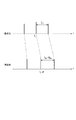
図8(a)に、数100pmの間隔で近接した複数の波長によるスペックル誤差および被検信号の強度の波長に対する関係を示す。図8(a)の■印のプロットは、被検面に入射する光のある波長を中心に近接した複数の波長によるスペックル誤差(左軸)を示し、図8(a)の●印のプロットは、基準光と被検面からの測定光との干渉光を測定して得られる被検信号の強度を示す。図8(a)より、被検信号の強度は波長によって変化することが分かる。これは、被検面の特性などで波長依存が生じているためと考えられる。また、スペックル誤差も波長により変化し、被検信号の強度が大きいとスペックル誤差が小さいことが分かる。つまり、被検信号の強度が大きい波長を用いることがスペックル誤差低減に有効であることを示す。 FIG. 8A shows the relationship between the speckle error due to a plurality of wavelengths that are close to each other at intervals of several hundred pm and the intensity of the signal under test with respect to the wavelength. The plot of ■ in FIG. 8A shows speckle errors (left axis) due to a plurality of wavelengths close to the center of a certain wavelength of light incident on the test surface. The plot shows the intensity of the test signal obtained by measuring the interference light between the reference light and the measurement light from the test surface. FIG. 8A shows that the intensity of the test signal changes depending on the wavelength. This is considered to be due to wavelength dependence due to the characteristics of the surface to be measured. The speckle error also changes depending on the wavelength, and it can be seen that the speckle error is small when the intensity of the signal under test is large. In other words, it is effective to use a wavelength having a high intensity of the test signal for reducing speckle errors.
図8(b)に、複数の波長を含む測定光の波長数と計測精度との関係を示す。図8(b)の■印のプロットは、測定光の最大波長差(最小波長と最大波長との差)が4.2THzの場合を示し、図8(b)の●印のプロットは最大波長差が9.5THzの場合を示す。図8(b)より、最大波長差を広げることで計測精度が向上することが分かる。これは、最大波長差を広げることにより、被検信号の強度が大きい波長を含むことができ、スペックル誤差が小さくなるためである。 FIG. 8B shows the relationship between the number of wavelengths of measurement light including a plurality of wavelengths and the measurement accuracy. The plot of ■ in FIG. 8B shows the case where the maximum wavelength difference (difference between the minimum wavelength and the maximum wavelength) of the measurement light is 4.2 THz, and the plot of ● in FIG. 8B is the maximum wavelength. A case where the difference is 9.5 THz is shown. FIG. 8B shows that the measurement accuracy is improved by widening the maximum wavelength difference. This is because by increasing the maximum wavelength difference, it is possible to include a wavelength with a high intensity of the test signal, and the speckle error is reduced.
また、図8(b)より、最大波長差を一定にして波長数を増やしていっても計測精度は飽和してしまい、ある一定値に収束することが分かる。そのため、最大波長差を変えずに波長数を増やすよりも、波長数を変えずに最大波長差を大きくする方が計測精度向上には良いという傾向があることが分かる。 Further, from FIG. 8B, it can be seen that even when the maximum wavelength difference is made constant and the number of wavelengths is increased, the measurement accuracy is saturated and converges to a certain value. Therefore, it can be seen that increasing the maximum wavelength difference without changing the number of wavelengths tends to improve the measurement accuracy rather than increasing the number of wavelengths without changing the maximum wavelength difference.
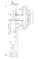
(第1実施形態)
図1は第1実施形態の光波干渉計測装置の構成図である。本実施形態の光波干渉計測装置は、図1に示すように複数の半導体レーザ1a、1b、1cと、入力された光束の強度または位相を互いに異なる変調周期で変調する変調素子3a、3bと、を有する多波長光源100(光源部)を計測用光源として用いる。変調素子として例えば電気光学変調素子が用いられる。多波長光源100からの2つの射出光束を基準光(第1光)と測定光(第2光)とする。計測装置は、基準光と被検面で反射する前の測定光とを干渉させて得られる参照信号と、基準光と被検面で反射した後の測定光とを干渉させて得られる被検信号から、測定対象の物体の被検面の位置を求める。
(First embodiment)
FIG. 1 is a configuration diagram of the optical interference measuring apparatus according to the first embodiment. As shown in FIG. 1, the optical interference measuring apparatus of the present embodiment includes a plurality of
以下、本実施形態の光波干渉計測装置について詳述する。半導体レーザ1a、1b、1cは、互いに異なる発振波長を有する単一縦モードレーザであり、各レーザは単一波長の光を射出する。これら半導体レーザは独立に波長制御することができるため、容易に半導体レーザ間の発振波長に大きな波長差をつけることができる。これにより、最大波長と最小波長との差が大きく、より広い波長帯域で発振可能な光源を構成することができる。半導体レーザの数は3つに限らず、2つでも良く、必要に応じて増やしてもよい。このような半導体レーザとしてDFBレーザを用いることにより、比較的安価に安定した単一モード発振を実現することができる。ただし、これに限定されるものではなく、外部共振器型半導体レーザ(ECLD)や面発光レーザ(VCSEL)を用いてもよい。また、それぞれ独立のレーザ素子である必要はなく、光通信用のDFBレーザのように多波長が集積化されたタイプのものを用いてもよい。これらのレーザは、高価な光周波数コム発生器よりも安価である。
Hereinafter, the light wave interference measuring apparatus of this embodiment will be described in detail. The
半導体レーザ1a、1b、1cからの光は、偏波面保持ファイバで射出され、偏波面保持タイプ3×2のファイバカプラ2により合波された後、2つに分波される。分波された光束はそれぞれ電気光学変調素子に入射する。分波された2つの光束のうち片方(測定光)は周波数シフタ4で周波数をシフトされた後に、電気光学変調素子に入射する。分波された2つの光束のもう片方(基準光)は周波数シフタ4を介さずに電気光学変調素子に入射する。なお、測定光の周波数をシフトする周波数シフタ4だけに限らず、基準光の光路にも周波数シフタを用いてもよい。つまり、測定光と基準光との周波数を異ならせるために、測定光と基準光の少なくとも一方の周波数をシフトすればよい。
Lights from the
電気光学変調素子は、入射光の強度または位相を変調し、入射光の周波数に対して周波数がずれたサイドバンドを有する光を生成する。分波されたそれぞれの光は、半導体レーザ1a、1b、1cからの互いに異なる波長の光を含むため、分波された光を電気光学変調素子で変調すると、半導体レーザからのそれぞれの光について、サイドバンドの周波数間隔を高精度に一致させることができる。高精度な粗面計測には、独立の半導体レーザで生成される広帯域な波長の全域に亘って測定値の平均を行う事が必要であるため、1つの電気光学変調素子によって生じる、各レーザからの光のサイドバンドの周波数間隔は一致している必要がある。
The electro-optic modulation element modulates the intensity or phase of incident light and generates light having a sideband whose frequency is shifted from the frequency of the incident light. Since each of the demultiplexed light includes light of different wavelengths from the
電気光学変調素子3a、3bとしては、例えば光通信で一般的な強度変調器が用いられる。これはニオブ酸リチウムを用いたマッハツェンダ干渉計構造をしており、強度変調により、等間隔に複数のサイドバンドを発生させる。変調周波数fmとし、(1+cos[2πfmt])の2乗の強度変調を発生させるとサイドバンドの本数を2本に抑えることができ、スペクトル一本当たりの光量を高くすることができる。そのため、被検面が粗面の場合のように比較的弱い散乱光を測定する必要がある場合でも、ノイズの影響を小さくでき、より高精度な計測が可能になる。
As the electro-
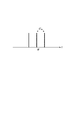
本実施形態では、強度変調器によってサイドバンドを2本発生させる場合について説明する。半導体レーザ1a、1b、1cの発振周波数をそれぞれf1、f2、f3とする。複数の半導体レーザからの光を共通の電気光学変調素子に通すことにより、図2のように、各レーザからの光について、等しいスペクトル間隔をもつ複数の狭帯域なスペクトルを有し、周波数f1〜f3までの広波長帯域の光を生成する。
In the present embodiment, a case where two sidebands are generated by an intensity modulator will be described. The oscillation frequencies of the
半導体レーザ1a、1b、1cの発振周波数をfi(i=1、2、3)とし、多波長光源100から射出される2つの光(基準光と測定光)のスペクトル分布を図3に示す。測定光は周波数シフタ4により、基準光に対してdfの周波数シフトを与えられる。基準光用の第1電気光学変調素子3aと、測定光用の第2電気光学変調素子3bとでは、強度または位相の変調周期が互いに異なる。そのため、第1電気光学変調素子3aの変調周波数は周波数fm、第2電気光学変調素子3bの変調周波数はfm+dfmであり、所定量dfmだけ異なる周波数に変調される。
測定光と基準光を干渉させた際にはそれぞれのスペクトル間の干渉が発生する。なお、fm>>df、dfmとしてサイドバンド間の干渉信号成分をローパスフィルタで除去すると、図4のように、周波数シフト量dfの周波数を中心として、両サイドに周波数dfmだけ離れたスペクトル分布を有するビート信号が得られる。横軸は信号の周波数である。dfは、第2電気光学変調素子3bに入射する測定光と第1電気光学変調素子3aに入射する基準光との周波数差に相当する。
When the measurement light and the reference light interfere with each other, interference between the respective spectra occurs. When the interference signal component between the sidebands is removed by a low-pass filter with f m >> df and df m , the frequency df m is separated on both sides with the frequency shift amount df as the center as shown in FIG. A beat signal having a spectral distribution is obtained. The horizontal axis is the frequency of the signal. df corresponds to a frequency difference between the measurement light incident on the second electro-
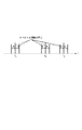
干渉計101に入射した基準光は、コリメートレンズ5aで平行光束とされ、λ/2板6aを透過後、偏光ビームスプリッタ7で2つに分波される。偏光ビームスプリッタ7で反射された基準光はλ/2板8を透過することで偏光方向が90度回転させられ、偏光ビームスプリッタ9及び偏光子10を透過した後、分光素子11aに入射する。また、干渉計101に入射した測定光は、コリメートレンズ5bで平行光束とされλ/2板6bを透過後、偏光ビームスプリッタ9で分波される。偏光ビームスプリッタ9で反射された測定光束は偏光子10を透過し、分光素子11aに入射する。
The reference light incident on the
一方、偏光ビームスプリッタ7を透過した基準光は、偏光ビームスプリッタ12及び偏光子13を透過後、分光器11bに入射する。また、偏光ビームスプリッタ9を透過した測定光束は偏光ビームスプリッタ12を透過後λ/4板14により円偏光とされ、集光レンズ15で集光光束となって被検面上に集光される。被検面で反射されて逆周りの円偏光とされた後、再度λ/4板14を透過することにより入射時とは偏波面が90度回転した直線偏光となって偏光ビームスプリッタ12に再度入射する。その後、偏光ビームスプリッタ12で反射され、偏光子13を透過後に分光素子11bに入射する。偏光子10、13により基準光と測定光の共通偏光成分を抽出することで干渉光を得るものとする。偏光ビームスプリッタ7、9で反射され、分光素子11aに入射する光路を参照光路、偏光ビームスプリッタ7、9を透過し、分光素子11bに入射する光路を被検光路と称す。
On the other hand, the reference light transmitted through the
分光素子11a、11bとしては、例えばアレイ導波路回折型波長分波器が用いられる。以下の説明において、アレイ導波路回折型波長分波器をAWGと称す。AWGは、光路長差の異なるアレイ上の導波路射出後の回折により分波する素子であり、小型で安価に入手可能である。分光素子11a、11bはAWGに限定されるものではなく、例えばバルク型の回折格子を用いてもよい。また、本実施形態の分光素子として、バンドパスの干渉フィルターを用いてもよい。このような干渉フィルターを用いると多波長光源の計測対象の波長数が少ない場合に、分光素子の構成が簡単になるという利点がある。
As the
分光素子11a、11bによって多波長光源100の半導体レーザからのそれぞれの光に分岐された光は、半導体レーザの数に対応して複数個の検出器を備えて構成された測定装置(測定部)16a、16bにて受光される。検出器は例えばフォトディテクタなどの光電変換素子、センサである。以下では、測定装置16aで測定される干渉光の信号を参照信号とし、測定装置16bで測定される干渉光の信号を被検信号と称す。プロセッサなどの処理部17は、測定装置16a,16bから出力される参照信号と被検信号の位相差を用いて被検面の位置(被検面までの距離)を算出する。複数点の被検面の位置を取得すれば被検面の形状を求めることができる。
The light branched into the light from the semiconductor laser of the multi-wavelength
次に、本実施形態の処理部17が行う演算処理について説明する。図5はそのフローチャートである。
Next, arithmetic processing performed by the
まず、処理部17は測定部による測定データを取得する。そして、S101において、半導体レーザ毎に得られる参照信号及び被検信号に対して、スペクトル毎(周波数毎)に得られる干渉信号の位相(干渉位相)を計測する。すなわち処理部17は、半導体レーザ毎に、複数の周波数についての各干渉信号から位相を計測する。干渉位相の計測は、位相計を構成することにより可能となる。例として、分光素子11a、11bで分岐された半導体レーザ1a(発振周波数はf1)からの光について説明する。測定装置16aで測定される半導体レーザ1aからの光の基準光と測定光の電場振幅Eref R、Etest Rはそれぞれ式(1)のように表わされる。
First, the

参照光路における基準光と測定光の強度変調信号の位相差をφ、光波の位相差をθとして表わしている。 The phase difference between the intensity modulation signal of the reference light and the measurement light in the reference optical path is represented by φ, and the phase difference of the light wave is represented by θ.
この基準光と測定光の電場振幅Eref R、Etest Rの干渉による参照信号IRefは式(2)のように表わすことができる。 The reference signal I Ref due to the interference between the electric field amplitudes E ref R and E test R of the reference light and the measurement light can be expressed as shown in Equation (2).
ただし、周波数(df+dfm)よりも高い成分はローパスフィルタにより除去するとして示していない。 However, a component higher than the frequency (df + df m ) is not shown as being removed by the low-pass filter.
同様に、被検信号ITestは式(3)のように表わすことができる。 Similarly, the test signal I Test can be expressed as Equation (3).
φ´とθ´は、被検光路における基準光と測定光の強度変調信号および光波の位相差として式(4)で表わされる。被検光路における基準光と測定光の光路長差をnDと称す。nは屈折率を表わし、屈折率の分散が無視できるものとする。屈折率nは、光波干渉計測装置の近傍において気圧、温度、湿度等の環境状態を計測し、計測波長に応じて屈折率の分散式からの計算により得られる。 φ ′ and θ ′ are expressed by Equation (4) as the phase difference between the intensity modulation signal of the reference light and the measurement light and the light wave in the test light path. The optical path length difference between the reference light and the measurement light in the test light path is referred to as nD. n represents a refractive index, and the dispersion of the refractive index can be ignored. The refractive index n is obtained by measuring environmental conditions such as atmospheric pressure, temperature, and humidity in the vicinity of the light wave interference measuring apparatus, and calculating from the refractive index dispersion formula according to the measurement wavelength.
周波数dfの信号を位相計で検出した場合の参照信号および被検信号の位相をそれぞれΦref dfと、Φtest dfとすると、以下の式(5)で表わされる。 When the phase of the reference signal and the signal to be detected when the signal of the frequency df is detected by the phase meter is Φ ref df and Φ test df , respectively, it is expressed by the following equation (5).
同様に周波数(df+dfm)の参照信号および被検信号の位相をΦref (df+dfm)と、Φtest (df+dfm)とし、以下の式(6)で表わされる。 Similarly, the phases of the reference signal and the test signal of the frequency (df + df m ) are Φ ref (df + dfm) and Φ test (df + dfm), and are expressed by the following formula (6).
また、周波数(df−dfm)の参照信号および被検信号の位相をΦref (df−dfm)と、Φtest (df−dfm)とし、以下の式(7)で表わされる。 Further, the phases of the reference signal and the test signal of the frequency (df−df m ) are Φ ref (df−dfm) and Φ test (df−dfm), and are expressed by the following equation (7).
次に、処理部17は、S102において、参照信号と被検信号間の位相差を計算する。位相差は、周波数df、周波数(df+dfm)、周波数(df−dfm)のそれぞれについて計算する。周波数dfにおける参照信号と被検信号間の位相差ΔΦ(df)は、上記式(5)の2式の差を算出することにより以下の式(8)のように得られる。
Next, the
同様に周波数(df+dfm)と(df−dfm)の参照信号および被検信号における位相差ΔΦ(df+dfm)、ΔΦ(df−dfm)は、以下の式(9)及び式(10)で表わされる。 Similarly, the phase differences ΔΦ (df + dfm) and ΔΦ (df−dfm) in the reference signal and the test signal of the frequencies (df + df m ) and (df−df m ) are expressed by the following expressions (9) and (10). It is.
次に、処理部17は、S103において、隣り合ったスペクトル間の位相差を計算する。隣り合ったスペクトル間の位相差は、以下の式(11)及び式(12)で表わされる。
Next, the
次に、処理部17は、S104において、上記(11)式及び(12)式より、被検光路における基準光と測定光の光路長差nDをそれぞれ算出し、以下の式(13)を用いて、それらの平均値nD1 aveを計算する。なお、光路長差nDが被検面の位置に相当する。
Next, in S104, the
S104で算出される光路長差nDは、隣り合ったスペクトルによってできる合成波長c/(fm+dfm)に対する計算値となっている。そのため、電気光学変調素子によって変調周波数fmを高くすることで、合成波長を短くすることができる。これにより、位相の計測精度を向上でき、光路長差を高精度に求めることができる。 Optical path length difference is calculated in S104 nD has a calculated value for the synthetic wavelength can be by adjacent spectrum c / (f m + df m ). Therefore, by increasing the modulation frequency f m by electro-optical modulation device, it is possible to shorten the synthetic wavelength. Thereby, the measurement accuracy of the phase can be improved, and the optical path length difference can be obtained with high accuracy.
以上S101〜S104の工程の説明は、半導体レーザ1aからの光を例に述べたが、半導体レーザ1b、1cについても同様に実施し、nD2 ave、nD3 aveを得る。
In the above description of the steps S101 to S104, the light from the
次に、ステップS105において、半導体レーザ毎に求められた光路長差の平均値nDi ave(i=1〜3)を平均し、最終出力値nDtotalを得る。式14に単純平均の例を示す。
Next, in step S105, an average value nD i ave (i = 1 to 3) of optical path length differences obtained for each semiconductor laser is averaged to obtain a final output value nD total .
半導体レーザ間の波長差が大きい場合、半導体レーザ毎の光路長差の平均値nDi aveはそれぞれスペックルの影響が異なる。したがって、半導体レーザ毎の光路長差の平均値nDi aveを平均化することでスペックル誤差を低減できる。 When the wavelength difference between the semiconductor lasers is large, the average value nD i ave of the optical path length difference for each semiconductor laser has different speckle effects. Therefore, the speckle error can be reduced by averaging the average value nD i ave of the optical path length difference for each semiconductor laser.
また、先述した通りスペックル誤差は被検信号の強度と相関があり、被検信号の強度が大きい波長を選択することが計測精度向上に有効である。したがって、nDi ave(i=1〜3)を平均する際に、半導体レーザ毎の被検信号の強度を重み(係数)として、加重平均をすることでさらに高精度な計測を実現できる。 Further, as described above, the speckle error has a correlation with the intensity of the test signal, and it is effective to improve the measurement accuracy to select a wavelength having a high intensity of the test signal. Therefore, when averaging nD i ave (i = 1 to 3), more accurate measurement can be realized by performing weighted averaging using the intensity of the test signal for each semiconductor laser as a weight (coefficient).
以上のとおり、本実施形態によれば、単一波長の光を射出するレーザを複数有し、各レーザの発振波長を異ならせて波長差を大きくすることによって、スペックル誤差による影響を小さくすることができる。したがって、より高精度に被検面の位置を計測可能な計測装置を提供することができる。 As described above, according to the present embodiment, the influence of speckle errors is reduced by having a plurality of lasers that emit light of a single wavelength and increasing the wavelength difference by changing the oscillation wavelength of each laser. be able to. Therefore, it is possible to provide a measuring device that can measure the position of the surface to be measured with higher accuracy.
モードロックレーザに代表される光周波数コム光源はモード周波数間隔が数10MHzと狭く、波長数が多いため、特に、被検面からの反射光が微弱となる粗面の計測においてはノイズにより計測精度が悪化してしまう。 An optical frequency comb light source typified by a mode-locked laser has a narrow mode frequency interval of several tens of MHz and a large number of wavelengths. Therefore, measurement accuracy due to noise is particularly high when measuring rough surfaces where reflected light from the surface to be measured is weak. Will get worse.
なお、電気光学変調素子3a、3bとして、強度変調器の代わりに位相変調器を用いてもよい。位相変調器は、変調周波数に対して高調波成分を容易に発生させることが可能である。具体的には、変調深さπで変調した場合にはベッセル関数で与えられる振幅は、基本波0.28、2倍波0.49、3倍波0.33であることが知られている。光アンプ等を用いることによりスペクトル一本当たりの光量低下が問題にならない場合は、位相変調器を用いた方がサイドバンドを増やすことによる平均化効果が得られるため、高精度化できる。
Note that a phase modulator may be used instead of the intensity modulator as the electro-
(第2実施形態)
図6に基づいて第2実施形態の光波干渉計測装置について説明する。図6は第2実施形態の光波干渉計測装置を示した図である。
(Second Embodiment)
Based on FIG. 6, the optical interference measuring apparatus of 2nd Embodiment is demonstrated. FIG. 6 is a diagram showing a lightwave interference measuring apparatus according to the second embodiment.
本実施形態の光波干渉計測装置は、図6に示されるように、多波長光源200の構成が第1実施形態とは異なる。本実施形態においては、多波長光源200は、複数の半導体レーザ1a、1b、1c毎に対応して、周波数シフタ4a、4b、4cを有し、半導体レーザからのそれぞれの光はそれぞれ異なる周波数シフト量dfi(i=1〜3)を与えられる。したがって、測定装置16a、16bで測定される基準光と被検光の干渉光の信号は、複数の半導体レーザ毎に異なる周波数dfi、dfi±dfmが多重化されたビート信号になる。図7に、各レーザによるビート信号のスペクトル分布を示す。横軸は信号の周波数である。
As shown in FIG. 6, the optical interference measurement apparatus of the present embodiment is different from the first embodiment in the configuration of the multi-wavelength
このように、各レーザでビート信号の周波数が異なるため、複数の半導体レーザの出力波長毎に干渉光を分光する分光素子が必要なく、測定装置の検出器は参照信号および被検信号それぞれ1つで済む。 In this way, since the frequency of the beat signal is different for each laser, there is no need for a spectroscopic element that separates interference light for each output wavelength of a plurality of semiconductor lasers, and there is one reference signal and one test signal for the detector of the measuring apparatus. Just do it.
以下、本実施形態の光波干渉計測装置について詳述する。複数の半導体レーザからの出力はそれぞれ偏波面保持タイプ1×2のファイバカプラ21a、21b、21cで分波され、一方は偏波面保持タイプ3×2のファイバカプラ22aで合波され、第1電気光学変調素子3aに入射する。もう一方はそれぞれ周波数シフト量が異なる周波数シフタ4a、4b、4cを介して偏波面保持タイプ3×2のファイバカプラ22bで合波され、第2電気光学変調素子3bに入射する。第1電気光学変調素子3aを射出した基準光と、第2電気光学変調素子3bを射出した測定光が干渉計201に入射し、分光素子を介さずに、測定装置16a、16bに入射する。第1電気光学変調素子3aを射出した基準光と、第2電気光学変調素子3bを射出した測定光が干渉計201に入射し、測定装置16a、16bに入射するまでの基本的な流れは第1実施形態と同じため、重複する説明は省く。干渉計201に分光素子が無い点で干渉計101とは異なる。
Hereinafter, the light wave interference measuring apparatus of this embodiment will be described in detail. Outputs from the plurality of semiconductor lasers are demultiplexed by polarization plane holding type 1 × 2
各レーザからの参照信号IRef及び被検信号ITestは、前記式(2)と式(3)におけるdfが、異なる3つの周波数df1、df2、df3となる。測定装置で測定されたビート信号の測定データを用いて、ある半導体レーザに対する周波数成分のみを同期検波する等により、各レーザに対応する信号を取り出すことができる。処理部27で計測される位相は式(5)、(6)、(7)におけるdfが各レーザで異なるだけで、基本的には同じである。光路長差を求めるための処理部27による演算処理は第1実施形態と同じため説明を省く。
The reference signal I Ref and the test signal I Test from each laser have three different frequencies df 1 , df 2 , and df 3 in which df in the equations (2) and (3) are different. A signal corresponding to each laser can be extracted by synchronously detecting only the frequency component for a certain semiconductor laser using the measurement data of the beat signal measured by the measuring device. The phase measured by the
本実施形態では、特定の半導体レーザに対する周波数成分のみを同期検波によって取り出す説明をしたが、多重化された干渉信号をフーリエ変換した後、特定の周波数成分の位相を取り出しても構わない。 In the present embodiment, only the frequency component for the specific semiconductor laser has been described by synchronous detection. However, the phase of the specific frequency component may be extracted after Fourier-transforming the multiplexed interference signal.
このように、本実施形態によれば、分光器および分光数に対応する複数の検出器を必要としないため、コンパクトかつ低コストな計測装置を提供することができる。 Thus, according to the present embodiment, a spectroscope and a plurality of detectors corresponding to the number of spectra are not required, and thus a compact and low-cost measuring device can be provided.
以上、本発明の好ましい実施形態について説明したが、本発明はこれらの実施形態に限定されず、その要旨の範囲内で種々の変形及び変更が可能である。 As mentioned above, although preferable embodiment of this invention was described, this invention is not limited to these embodiment, A various deformation | transformation and change are possible within the range of the summary.
<物品の製造方法の実施形態>
本実施形態における物品の製造方法は、例えば、ギアなどの金属部品や光学素子等の物品を加工する際に用いられる。本実施形態の物品の加工方法は、上記の計測装置を用いて、上記物品の被検面の形状を計測する工程と、かかる工程における計測結果に基づいて被検面を加工する工程とを含む。例えば、被検面の形状を計測装置を用いて計測し、その計測結果に基づいて、被検面の形状が設計値など所望の形状になるように当該被検面を加工する。上記計測装置により高精度に被検面の形状を計測できるため、本実施形態の物品の製造方法は、従来の方法に比べて、少なくとも物品の加工精度の点で有利である。
<Embodiment of Method for Manufacturing Article>
The method for manufacturing an article in the present embodiment is used, for example, when processing an article such as a metal part such as a gear or an optical element. The article processing method of the present embodiment includes a step of measuring the shape of the test surface of the article using the measuring device, and a step of processing the test surface based on the measurement result in the process. . For example, the shape of the test surface is measured using a measuring device, and based on the measurement result, the test surface is processed so that the shape of the test surface becomes a desired shape such as a design value. Since the shape of the test surface can be measured with high accuracy by the measuring device, the article manufacturing method of the present embodiment is advantageous in at least the processing accuracy of the article as compared with the conventional method.
Claims (15)
光源からの光を第1光と第2光に分け、前記第1光と前記第2光を周波数を異ならせて射出する光源部と
前記光源部から射出された前記第1光と前記被検面で反射する前の前記第2光とを干渉させ、前記光源部から射出された前記第1光と前記被検面で反射した後の前記第2光とを干渉させる干渉計と、
前記干渉計による干渉光を測定する測定部と、
前記測定部による測定データを用いて前記被検面の位置を求める処理部と、を有し、
前記光源部は、
レーザを複数有し、
複数の前記レーザはそれぞれで波長が互いに異なる光を射出し、前記レーザからの光を前記第1光と前記第2光に分け、
複数の前記レーザからの複数の前記第1光の強度または位相を変調する第1変調素子と、
複数の前記レーザからの複数の前記第2光の強度または位相を変調する第2変調素子とを有し、
前記第1変調素子と前記第2変調素子との変調周期が互いに異なることを特徴とする計測装置。 A measuring device for measuring the position of a surface to be tested,
The light from the light source is divided into the first light and the second light, the light source part that emits the first light and the second light with different frequencies, the first light emitted from the light source part, and the test object An interferometer that interferes with the second light before being reflected by a surface, and that causes the first light emitted from the light source unit to interfere with the second light after being reflected by the test surface;
A measurement unit for measuring interference light by the interferometer;
A processing unit for determining the position of the test surface using measurement data obtained by the measurement unit,
The light source unit is
Have multiple lasers,
The plurality of lasers emit light having different wavelengths from each other, and split the light from the laser into the first light and the second light,
A first modulation element that modulates the intensity or phase of the plurality of first lights from the plurality of lasers;
A second modulation element that modulates the intensity or phase of the plurality of second lights from the plurality of lasers,
The measuring apparatus, wherein the first modulation element and the second modulation element have different modulation periods.
第2の前記レーザからの光の周波数をシフトさせる第2周波数シフタとを有し、
前記第1周波数シフタと前記第2周波数シフタで周波数シフト量が互いに異なることを特徴とする請求項1乃至3の何れか1項に記載の計測装置。 A first frequency shifter for shifting the frequency of light from the first laser;
A second frequency shifter for shifting the frequency of light from the second laser,
4. The measuring apparatus according to claim 1, wherein the first frequency shifter and the second frequency shifter have different frequency shift amounts. 5.
前記周波数のずれ量は、前記第1変調素子と前記第2変調素子とで所定量だけ異なることを特徴とする請求項1乃至7の何れか1項に記載の計測装置。 Each of the first modulation element and the second modulation element generates light having two sidebands shifted in frequency with respect to the frequency of incident light,
The measuring apparatus according to claim 1, wherein the frequency shift amount differs by a predetermined amount between the first modulation element and the second modulation element.
計測された形状に基づいて前記被検面を加工する工程とを有することを特徴とする物品の製造方法。 A step of measuring the shape of the test surface of the article using the measuring device according to claim 1;
And a step of processing the surface to be measured based on the measured shape.
レーザを複数有し、
複数の前記レーザはそれぞれで波長が互いに異なる光を射出し、前記レーザからの光を前記第1光と前記第2光とに分け、
複数の前記レーザからの複数の前記第1光の強度または位相を変調する第1変調素子と、
複数の前記レーザからの複数の前記第2光の強度または位相を変調する第2変調素子とを有し、
前記第1変調素子と前記第2変調素子との変調周期が互いに異なることを特徴とする光源装置。 A light source device that divides light from a light source into first light and second light, and emits the first light and the second light at different frequencies,
Have multiple lasers,
The plurality of lasers emit light having different wavelengths from each other, and the light from the laser is divided into the first light and the second light,
A first modulation element that modulates the intensity or phase of the plurality of first lights from the plurality of lasers;
A second modulation element that modulates the intensity or phase of the plurality of second lights from the plurality of lasers,
The light source device, wherein the first modulation element and the second modulation element have different modulation periods.
レーザからの光を第1光と第2光に分け、前記第1光と前記第2光を周波数を異ならせて射出する射出ステップと、
前記第1光と前記被検面で反射する前の前記第2光とを干渉させ、前記第1光と前記被検面で反射した後の前記第2光とを干渉させ、干渉光の測定データを用いて前記被検面の位置を求めるステップと、を有し、
前記射出ステップにおいて、
それぞれで波長が互いに異なる光を射出する複数のレーザからのそれぞれの光を前記第1光と前記第2光に分け、
複数の前記レーザからの複数の前記第1光の強度または位相を変調し、
複数の前記レーザからの複数の前記第2光の強度または位相を変調し、
前記第1光の強度または位相の変調周期と前記第2光の強度または位相の変調周期とが互いに異なることを特徴とする計測方法。 A measurement method for measuring the position of a test surface,
An emission step of dividing light from the laser into first light and second light, and emitting the first light and the second light at different frequencies;
Interfering the first light and the second light before being reflected by the test surface, causing the first light and the second light after being reflected by the test surface to be interfered, and measuring interference light Determining the position of the test surface using data,
In the injection step,
Dividing each light from a plurality of lasers emitting light having different wavelengths from each other into the first light and the second light,
Modulating the intensity or phase of a plurality of the first lights from a plurality of the lasers;
Modulating the intensity or phase of a plurality of the second lights from a plurality of the lasers;
The measurement method, wherein the intensity or phase modulation period of the first light and the intensity or phase modulation period of the second light are different from each other.
Priority Applications (1)
| Application Number | Priority Date | Filing Date | Title |
|---|---|---|---|
| JP2013017172A JP2014149190A (en) | 2013-01-31 | 2013-01-31 | Measuring device, measuring method, light source device, and article manufacturing method |
Applications Claiming Priority (1)
| Application Number | Priority Date | Filing Date | Title |
|---|---|---|---|
| JP2013017172A JP2014149190A (en) | 2013-01-31 | 2013-01-31 | Measuring device, measuring method, light source device, and article manufacturing method |
Publications (1)
| Publication Number | Publication Date |
|---|---|
| JP2014149190A true JP2014149190A (en) | 2014-08-21 |
Family
ID=51572288
Family Applications (1)
| Application Number | Title | Priority Date | Filing Date |
|---|---|---|---|
| JP2013017172A Pending JP2014149190A (en) | 2013-01-31 | 2013-01-31 | Measuring device, measuring method, light source device, and article manufacturing method |
Country Status (1)
| Country | Link |
|---|---|
| JP (1) | JP2014149190A (en) |
Cited By (4)
| Publication number | Priority date | Publication date | Assignee | Title |
|---|---|---|---|---|
| JP2015094760A (en) * | 2013-11-08 | 2015-05-18 | ザ・ボーイング・カンパニーTheBoeing Company | Synthetic wave laser ranging sensors and methods |
| CN109804294A (en) * | 2016-10-25 | 2019-05-24 | 林瑟科技公司 | Optical fiber splitter device and optical system including the optical fiber splitter device for digital hologram imaging and interferometry |
| CN114295583A (en) * | 2021-11-26 | 2022-04-08 | 中国地质调查局水文地质环境地质调查中心 | Coherent measurement device for greenhouse gas |
| JP7472468B2 (en) | 2019-03-20 | 2024-04-23 | 株式会社リコー | Illumination devices, projection devices, measuring devices, robots, electronic devices, moving objects, and modeling devices |
-
2013
- 2013-01-31 JP JP2013017172A patent/JP2014149190A/en active Pending
Cited By (8)
| Publication number | Priority date | Publication date | Assignee | Title |
|---|---|---|---|---|
| JP2015094760A (en) * | 2013-11-08 | 2015-05-18 | ザ・ボーイング・カンパニーTheBoeing Company | Synthetic wave laser ranging sensors and methods |
| CN109804294A (en) * | 2016-10-25 | 2019-05-24 | 林瑟科技公司 | Optical fiber splitter device and optical system including the optical fiber splitter device for digital hologram imaging and interferometry |
| JP2019533839A (en) * | 2016-10-25 | 2019-11-21 | リンシー・テック・ソシエテ・アノニム | Fiber splitter device for digital holographic imaging and interferometry and optical system including said fiber splitter device |
| US11340438B2 (en) | 2016-10-25 | 2022-05-24 | Lyncee Tec Sa | Fiber splitter device for digital holographic imaging and interferometry and optical system comprising said fiber splitter device |
| JP7187467B2 (en) | 2016-10-25 | 2022-12-12 | リンシー・テック・ソシエテ・アノニム | Fiber splitter device for digital holographic imaging and interferometry and optical system containing said fiber splitter device |
| JP7472468B2 (en) | 2019-03-20 | 2024-04-23 | 株式会社リコー | Illumination devices, projection devices, measuring devices, robots, electronic devices, moving objects, and modeling devices |
| CN114295583A (en) * | 2021-11-26 | 2022-04-08 | 中国地质调查局水文地质环境地质调查中心 | Coherent measurement device for greenhouse gas |
| CN114295583B (en) * | 2021-11-26 | 2023-12-26 | 中国地质调查局水文地质环境地质调查中心 | Coherent measurement device for greenhouse gas |
Similar Documents
| Publication | Publication Date | Title |
|---|---|---|
| US8363226B2 (en) | Optical interference measuring apparatus | |
| US10168137B2 (en) | Dual laser frequency sweep interferometry system and method | |
| US8699013B2 (en) | Chromatic dispersion measurement device and chromatic dispersion measurement method for measuring the dispersion of light pulses | |
| US20090207418A1 (en) | Absolute distance measurement method and system using optical frequency generator | |
| US9506739B2 (en) | Distance measurement by beating a varying test signal with reference signal having absolute frequency value predetermined with a specified accuracy | |
| CN108873007B (en) | Frequency modulation continuous wave laser ranging device for inhibiting vibration effect | |
| JP5736247B2 (en) | Distance measuring method and apparatus | |
| JP5563439B2 (en) | Optical phase measuring device, optical phase measuring method and program | |
| RU102256U1 (en) | DEVICE FOR MEASURING PHYSICAL FIELD PARAMETERS | |
| JP2010203860A (en) | Vibration measuring device and vibration measuring method | |
| Lu et al. | Dual-channel self-mixing vibration measurement system in a linear cavity fiber laser | |
| JP2013181780A (en) | Measuring instrument and method for manufacturing article | |
| JP2015530598A (en) | Position monitoring system with reduced noise | |
| JP5363231B2 (en) | Vibration measuring apparatus and vibration measuring method | |
| JP2010261890A (en) | Light wave interference measuring device | |
| JP2014149190A (en) | Measuring device, measuring method, light source device, and article manufacturing method | |
| JP2013083581A (en) | Measuring device | |
| JP5421013B2 (en) | Positioning device and positioning method | |
| JP6264547B2 (en) | Optical signal generation apparatus, distance measurement apparatus, spectral characteristic measurement apparatus, frequency characteristic measurement apparatus, and optical signal generation method | |
| JP5468836B2 (en) | Measuring apparatus and measuring method | |
| JP2006308531A (en) | Wavelength dispersion measuring method and device | |
| Morozov et al. | Optical vector analyzer based on double-side modulation with a suppressed carrier and phase-shift FBG | |
| KR101108693B1 (en) | Refractive index measurement device based on white light interferometry and method thereof | |
| JP3905780B2 (en) | Brillouin spectral distribution measuring method and apparatus | |
| JP2014092425A (en) | Optical interference tomographic imaging apparatus and optical interference tomographic imaging method |