JP2014036081A - Method for manufacturing electronic device, electronic device, electronic equipment, and movable body - Google Patents
Method for manufacturing electronic device, electronic device, electronic equipment, and movable body Download PDFInfo
- Publication number
- JP2014036081A JP2014036081A JP2012175752A JP2012175752A JP2014036081A JP 2014036081 A JP2014036081 A JP 2014036081A JP 2012175752 A JP2012175752 A JP 2012175752A JP 2012175752 A JP2012175752 A JP 2012175752A JP 2014036081 A JP2014036081 A JP 2014036081A
- Authority
- JP
- Japan
- Prior art keywords
- lid
- electronic device
- package
- sealing hole
- manufacturing
- Prior art date
- Legal status (The legal status is an assumption and is not a legal conclusion. Google has not performed a legal analysis and makes no representation as to the accuracy of the status listed.)
- Withdrawn
Links
- 238000000034 method Methods 0.000 title claims abstract description 33
- 238000004519 manufacturing process Methods 0.000 title claims abstract description 32
- 238000007789 sealing Methods 0.000 claims abstract description 105
- 238000003466 welding Methods 0.000 claims abstract description 19
- 230000001678 irradiating effect Effects 0.000 claims abstract description 7
- 238000005304 joining Methods 0.000 claims description 26
- 229910052751 metal Inorganic materials 0.000 claims description 22
- 239000002184 metal Substances 0.000 claims description 22
- 239000010931 gold Substances 0.000 claims description 20
- BQCADISMDOOEFD-UHFFFAOYSA-N Silver Chemical compound [Ag] BQCADISMDOOEFD-UHFFFAOYSA-N 0.000 claims description 17
- 229910052709 silver Inorganic materials 0.000 claims description 17
- 239000004332 silver Substances 0.000 claims description 17
- 238000005219 brazing Methods 0.000 claims description 16
- 238000004080 punching Methods 0.000 claims description 13
- PCHJSUWPFVWCPO-UHFFFAOYSA-N gold Chemical compound [Au] PCHJSUWPFVWCPO-UHFFFAOYSA-N 0.000 claims description 10
- 229910052737 gold Inorganic materials 0.000 claims description 10
- ATJFFYVFTNAWJD-UHFFFAOYSA-N Tin Chemical compound [Sn] ATJFFYVFTNAWJD-UHFFFAOYSA-N 0.000 claims description 8
- 229910045601 alloy Inorganic materials 0.000 claims description 8
- 239000000956 alloy Substances 0.000 claims description 8
- 238000002360 preparation method Methods 0.000 claims description 5
- 229910000679 solder Inorganic materials 0.000 claims description 4
- 239000013078 crystal Substances 0.000 abstract description 24
- PXHVJJICTQNCMI-UHFFFAOYSA-N Nickel Chemical compound [Ni] PXHVJJICTQNCMI-UHFFFAOYSA-N 0.000 description 18
- 230000002093 peripheral effect Effects 0.000 description 16
- 239000000463 material Substances 0.000 description 10
- 239000012298 atmosphere Substances 0.000 description 9
- 230000008018 melting Effects 0.000 description 7
- 238000002844 melting Methods 0.000 description 7
- 239000010453 quartz Substances 0.000 description 7
- VYPSYNLAJGMNEJ-UHFFFAOYSA-N silicon dioxide Inorganic materials O=[Si]=O VYPSYNLAJGMNEJ-UHFFFAOYSA-N 0.000 description 7
- 229910052759 nickel Inorganic materials 0.000 description 6
- 238000007747 plating Methods 0.000 description 6
- 239000000853 adhesive Substances 0.000 description 5
- 230000001070 adhesive effect Effects 0.000 description 5
- 238000010438 heat treatment Methods 0.000 description 5
- 229910000833 kovar Inorganic materials 0.000 description 5
- 230000000694 effects Effects 0.000 description 4
- 230000005284 excitation Effects 0.000 description 4
- 239000004593 Epoxy Substances 0.000 description 2
- KRHYYFGTRYWZRS-UHFFFAOYSA-N Fluorane Chemical compound F KRHYYFGTRYWZRS-UHFFFAOYSA-N 0.000 description 2
- 230000001133 acceleration Effects 0.000 description 2
- 239000003795 chemical substances by application Substances 0.000 description 2
- 239000011651 chromium Substances 0.000 description 2
- 230000007797 corrosion Effects 0.000 description 2
- 238000005260 corrosion Methods 0.000 description 2
- 238000007872 degassing Methods 0.000 description 2
- 238000000605 extraction Methods 0.000 description 2
- 239000010419 fine particle Substances 0.000 description 2
- 229910052451 lead zirconate titanate Inorganic materials 0.000 description 2
- 238000001465 metallisation Methods 0.000 description 2
- 238000012545 processing Methods 0.000 description 2
- 230000035939 shock Effects 0.000 description 2
- 229920003002 synthetic resin Polymers 0.000 description 2
- 239000000057 synthetic resin Substances 0.000 description 2
- 238000007740 vapor deposition Methods 0.000 description 2
- WSMQKESQZFQMFW-UHFFFAOYSA-N 5-methyl-pyrazole-3-carboxylic acid Chemical compound CC1=CC(C(O)=O)=NN1 WSMQKESQZFQMFW-UHFFFAOYSA-N 0.000 description 1
- 241000251468 Actinopterygii Species 0.000 description 1
- PIGFYZPCRLYGLF-UHFFFAOYSA-N Aluminum nitride Chemical compound [Al]#N PIGFYZPCRLYGLF-UHFFFAOYSA-N 0.000 description 1
- VYZAMTAEIAYCRO-UHFFFAOYSA-N Chromium Chemical compound [Cr] VYZAMTAEIAYCRO-UHFFFAOYSA-N 0.000 description 1
- 229910000640 Fe alloy Inorganic materials 0.000 description 1
- WQZGKKKJIJFFOK-GASJEMHNSA-N Glucose Natural products OC[C@H]1OC(O)[C@H](O)[C@@H](O)[C@@H]1O WQZGKKKJIJFFOK-GASJEMHNSA-N 0.000 description 1
- XEEYBQQBJWHFJM-UHFFFAOYSA-N Iron Chemical compound [Fe] XEEYBQQBJWHFJM-UHFFFAOYSA-N 0.000 description 1
- 229910013641 LiNbO 3 Inorganic materials 0.000 description 1
- 239000004642 Polyimide Substances 0.000 description 1
- XLOMVQKBTHCTTD-UHFFFAOYSA-N Zinc monoxide Chemical compound [Zn]=O XLOMVQKBTHCTTD-UHFFFAOYSA-N 0.000 description 1
- 239000008280 blood Substances 0.000 description 1
- 210000004369 blood Anatomy 0.000 description 1
- 230000036772 blood pressure Effects 0.000 description 1
- 229910010293 ceramic material Inorganic materials 0.000 description 1
- 229910052804 chromium Inorganic materials 0.000 description 1
- 229910017052 cobalt Inorganic materials 0.000 description 1
- 239000010941 cobalt Substances 0.000 description 1
- GUTLYIVDDKVIGB-UHFFFAOYSA-N cobalt atom Chemical compound [Co] GUTLYIVDDKVIGB-UHFFFAOYSA-N 0.000 description 1
- 238000004891 communication Methods 0.000 description 1
- 238000012790 confirmation Methods 0.000 description 1
- 238000007796 conventional method Methods 0.000 description 1
- 230000006837 decompression Effects 0.000 description 1
- 238000000151 deposition Methods 0.000 description 1
- PSHMSSXLYVAENJ-UHFFFAOYSA-N dilithium;[oxido(oxoboranyloxy)boranyl]oxy-oxoboranyloxyborinate Chemical compound [Li+].[Li+].O=BOB([O-])OB([O-])OB=O PSHMSSXLYVAENJ-UHFFFAOYSA-N 0.000 description 1
- 238000005553 drilling Methods 0.000 description 1
- 238000010894 electron beam technology Methods 0.000 description 1
- 229910052732 germanium Inorganic materials 0.000 description 1
- GNPVGFCGXDBREM-UHFFFAOYSA-N germanium atom Chemical compound [Ge] GNPVGFCGXDBREM-UHFFFAOYSA-N 0.000 description 1
- 239000008103 glucose Substances 0.000 description 1
- 239000011261 inert gas Substances 0.000 description 1
- 239000011810 insulating material Substances 0.000 description 1
- HFGPZNIAWCZYJU-UHFFFAOYSA-N lead zirconate titanate Chemical compound [O-2].[O-2].[O-2].[O-2].[O-2].[Ti+4].[Zr+4].[Pb+2] HFGPZNIAWCZYJU-UHFFFAOYSA-N 0.000 description 1
- GQYHUHYESMUTHG-UHFFFAOYSA-N lithium niobate Chemical compound [Li+].[O-][Nb](=O)=O GQYHUHYESMUTHG-UHFFFAOYSA-N 0.000 description 1
- 229910052574 oxide ceramic Inorganic materials 0.000 description 1
- 239000011224 oxide ceramic Substances 0.000 description 1
- TWNQGVIAIRXVLR-UHFFFAOYSA-N oxo(oxoalumanyloxy)alumane Chemical compound O=[Al]O[Al]=O TWNQGVIAIRXVLR-UHFFFAOYSA-N 0.000 description 1
- 238000000206 photolithography Methods 0.000 description 1
- 229920001721 polyimide Polymers 0.000 description 1
- 229920001296 polysiloxane Polymers 0.000 description 1
- 230000002265 prevention Effects 0.000 description 1
- 229920005989 resin Polymers 0.000 description 1
- 239000011347 resin Substances 0.000 description 1
- 238000007665 sagging Methods 0.000 description 1
- 229910052710 silicon Inorganic materials 0.000 description 1
- 239000010703 silicon Substances 0.000 description 1
- 238000005245 sintering Methods 0.000 description 1
- 238000004544 sputter deposition Methods 0.000 description 1
- 230000006641 stabilisation Effects 0.000 description 1
- 238000011105 stabilization Methods 0.000 description 1
- 239000010935 stainless steel Substances 0.000 description 1
- 229910001220 stainless steel Inorganic materials 0.000 description 1
- 239000000758 substrate Substances 0.000 description 1
- 238000001039 wet etching Methods 0.000 description 1
Images


Classifications
-
- H—ELECTRICITY
- H05—ELECTRIC TECHNIQUES NOT OTHERWISE PROVIDED FOR
- H05K—PRINTED CIRCUITS; CASINGS OR CONSTRUCTIONAL DETAILS OF ELECTRIC APPARATUS; MANUFACTURE OF ASSEMBLAGES OF ELECTRICAL COMPONENTS
- H05K3/00—Apparatus or processes for manufacturing printed circuits
- H05K3/30—Assembling printed circuits with electric components, e.g. with resistor
-
- H—ELECTRICITY
- H01—ELECTRIC ELEMENTS
- H01L—SEMICONDUCTOR DEVICES NOT COVERED BY CLASS H10
- H01L23/00—Details of semiconductor or other solid state devices
- H01L23/02—Containers; Seals
- H01L23/10—Containers; Seals characterised by the material or arrangement of seals between parts, e.g. between cap and base of the container or between leads and walls of the container
-
- H—ELECTRICITY
- H01—ELECTRIC ELEMENTS
- H01L—SEMICONDUCTOR DEVICES NOT COVERED BY CLASS H10
- H01L21/00—Processes or apparatus adapted for the manufacture or treatment of semiconductor or solid state devices or of parts thereof
- H01L21/02—Manufacture or treatment of semiconductor devices or of parts thereof
- H01L21/04—Manufacture or treatment of semiconductor devices or of parts thereof the devices having at least one potential-jump barrier or surface barrier, e.g. PN junction, depletion layer or carrier concentration layer
- H01L21/50—Assembly of semiconductor devices using processes or apparatus not provided for in a single one of the subgroups H01L21/06 - H01L21/326, e.g. sealing of a cap to a base of a container
- H01L21/54—Providing fillings in containers, e.g. gas fillings
-
- H—ELECTRICITY
- H05—ELECTRIC TECHNIQUES NOT OTHERWISE PROVIDED FOR
- H05K—PRINTED CIRCUITS; CASINGS OR CONSTRUCTIONAL DETAILS OF ELECTRIC APPARATUS; MANUFACTURE OF ASSEMBLAGES OF ELECTRICAL COMPONENTS
- H05K7/00—Constructional details common to different types of electric apparatus
- H05K7/02—Arrangements of circuit components or wiring on supporting structure
-
- H—ELECTRICITY
- H01—ELECTRIC ELEMENTS
- H01L—SEMICONDUCTOR DEVICES NOT COVERED BY CLASS H10
- H01L2924/00—Indexing scheme for arrangements or methods for connecting or disconnecting semiconductor or solid-state bodies as covered by H01L24/00
- H01L2924/0001—Technical content checked by a classifier
- H01L2924/0002—Not covered by any one of groups H01L24/00, H01L24/00 and H01L2224/00
-
- H—ELECTRICITY
- H03—ELECTRONIC CIRCUITRY
- H03H—IMPEDANCE NETWORKS, e.g. RESONANT CIRCUITS; RESONATORS
- H03H3/00—Apparatus or processes specially adapted for the manufacture of impedance networks, resonating circuits, resonators
- H03H3/007—Apparatus or processes specially adapted for the manufacture of impedance networks, resonating circuits, resonators for the manufacture of electromechanical resonators or networks
- H03H3/0072—Apparatus or processes specially adapted for the manufacture of impedance networks, resonating circuits, resonators for the manufacture of electromechanical resonators or networks of microelectro-mechanical resonators or networks
-
- H—ELECTRICITY
- H03—ELECTRONIC CIRCUITRY
- H03H—IMPEDANCE NETWORKS, e.g. RESONANT CIRCUITS; RESONATORS
- H03H3/00—Apparatus or processes specially adapted for the manufacture of impedance networks, resonating circuits, resonators
- H03H3/007—Apparatus or processes specially adapted for the manufacture of impedance networks, resonating circuits, resonators for the manufacture of electromechanical resonators or networks
- H03H3/02—Apparatus or processes specially adapted for the manufacture of impedance networks, resonating circuits, resonators for the manufacture of electromechanical resonators or networks for the manufacture of piezoelectric or electrostrictive resonators or networks
-
- H—ELECTRICITY
- H03—ELECTRONIC CIRCUITRY
- H03H—IMPEDANCE NETWORKS, e.g. RESONANT CIRCUITS; RESONATORS
- H03H9/00—Networks comprising electromechanical or electro-acoustic devices; Electromechanical resonators
- H03H9/02—Details
- H03H9/05—Holders; Supports
- H03H9/10—Mounting in enclosures
-
- Y—GENERAL TAGGING OF NEW TECHNOLOGICAL DEVELOPMENTS; GENERAL TAGGING OF CROSS-SECTIONAL TECHNOLOGIES SPANNING OVER SEVERAL SECTIONS OF THE IPC; TECHNICAL SUBJECTS COVERED BY FORMER USPC CROSS-REFERENCE ART COLLECTIONS [XRACs] AND DIGESTS
- Y10—TECHNICAL SUBJECTS COVERED BY FORMER USPC
- Y10T—TECHNICAL SUBJECTS COVERED BY FORMER US CLASSIFICATION
- Y10T29/00—Metal working
- Y10T29/49—Method of mechanical manufacture
- Y10T29/49002—Electrical device making
- Y10T29/49117—Conductor or circuit manufacturing
- Y10T29/49124—On flat or curved insulated base, e.g., printed circuit, etc.
- Y10T29/4913—Assembling to base an electrical component, e.g., capacitor, etc.
- Y10T29/49144—Assembling to base an electrical component, e.g., capacitor, etc. by metal fusion
Landscapes
- Engineering & Computer Science (AREA)
- Microelectronics & Electronic Packaging (AREA)
- Physics & Mathematics (AREA)
- Condensed Matter Physics & Semiconductors (AREA)
- General Physics & Mathematics (AREA)
- Computer Hardware Design (AREA)
- Power Engineering (AREA)
- Manufacturing & Machinery (AREA)
- Piezo-Electric Or Mechanical Vibrators, Or Delay Or Filter Circuits (AREA)
Abstract
Description
本発明は、電子デバイスの内部空間を減圧封止するための電子デバイスの製造方法、当該製造方法により製造された電子デバイス、および当該電子デバイスを搭載した電子機器と移動体とに関する。 The present invention relates to an electronic device manufacturing method for sealing an internal space of an electronic device under reduced pressure, an electronic device manufactured by the manufacturing method, and an electronic apparatus and a moving body on which the electronic device is mounted.
従来、電子デバイスの内部空間を減圧封止する方法としては、特許文献1に開示されているように、電子デバイスのパッケージを形成する工程と、パッケージ内部に電子部品を実装する工程と、パッケージに蓋体を溶接する工程と、において、蓋体を溶接する工程では、蓋体の周縁の一部領域を残し、残した領域以外の部分において蓋体とパッケージとのシーム溶接を行う。そして、パッケージを真空雰囲気内で加熱して、シーム溶接せずに残した一部領域からパッケージ内部の脱ガスをした後、当該一部領域に加熱ビームを照射することにより、パッケージ内部を減圧状態に封止していた。この方法によれば、これまで行われていた工程、即ち脱ガス用にパッケージあるいは蓋体に貫通孔を開ける工程や貫通孔をロウ材等で塞ぐ工程、が不要となり、工程の簡略化が図られた。 Conventionally, as disclosed in Patent Document 1, as a method for sealing the internal space of an electronic device under reduced pressure, a step of forming a package of the electronic device, a step of mounting electronic components inside the package, In the step of welding the lid body and the step of welding the lid body, a part of the periphery of the lid body is left, and seam welding between the lid body and the package is performed in a portion other than the remaining area. Then, after heating the package in a vacuum atmosphere and degassing the inside of the package from a partial area left without seam welding, the inside of the package is decompressed by irradiating the partial area with a heating beam. It was sealed. According to this method, the steps that have been performed up to now, that is, the step of opening a through hole in a package or lid for degassing and the step of closing the through hole with a brazing material, etc. are unnecessary, and the process can be simplified. It was.
しかし、従来の技術は、パッケージと、蓋体またはシームリングと、の位置関係がズレている場合等において、溶接せずに残しておくべき一部領域の大きさ(長さ)がばらついてしまうことがあった。この場合、当該一部領域によって、加熱ビームで封止する大きさ(長さ)が異なってしまうと、加熱ビームで封止されない未封止部分が生じる恐れがあった。また、未封止部分の発生を防止するために、加熱ビームの照射範囲を予め大きくしておくと、既にシーム溶接した部分を再度照射する範囲が増えることになり、その際にアウトガスが発生してパッケージ内部の減圧状態が低下する、という課題があった。これは、電子デバイスが小型化されるに伴って、より顕著になっていた。 However, in the conventional technique, when the positional relationship between the package and the lid or the seam ring is shifted, the size (length) of a partial region that should be left without welding varies. There was a thing. In this case, if the size (length) to be sealed with the heating beam varies depending on the partial region, there is a possibility that an unsealed portion that is not sealed with the heating beam may be generated. In addition, if the irradiation range of the heating beam is enlarged in advance in order to prevent the occurrence of unsealed portions, the range where the seam-welded portion is irradiated again increases, and outgas is generated at that time. As a result, there is a problem that the decompressed state inside the package is lowered. This has become more prominent as electronic devices are miniaturized.
本発明は、上述の課題の少なくとも一部を解決するためになされたものであり、以下の適用例または形態として実現することが可能である。 SUMMARY An advantage of some aspects of the invention is to solve at least a part of the problems described above, and the invention can be implemented as the following application examples or forms.
[適用例1]本適用例に係る電子デバイスの製造方法は、封止孔を有する蓋体と、メタライズ部を有し前記蓋体と共に内部空間を構成するためのパッケージと、電子部品とを用意する準備工程と、前記電子部品を前記パッケージに搭載する搭載工程と、前記封止孔と前記メタライズ部とが平面視で重なるように前記蓋体を前記パッケージに載置する載置工程と、前記蓋体の外周部と前記パッケージとをシーム溶接する第1接合工程と、エネルギービームを照射して前記封止孔と前記メタライズ部とを接合し前記封止孔と前記内部空間とを封止する第2接合工程と、を含むことを特徴とする。 Application Example 1 An electronic device manufacturing method according to this application example includes a lid body having a sealing hole, a package having a metallized portion and forming an internal space together with the lid body, and an electronic component. A preparatory step, a mounting step of mounting the electronic component on the package, a mounting step of mounting the lid on the package such that the sealing hole and the metallized portion overlap in plan view, A first joining step of seam welding the outer peripheral portion of the lid and the package; and irradiating an energy beam to join the sealing hole and the metallized portion to seal the sealing hole and the internal space. And a second joining step.
本適用例の電子デバイスの製造方法によれば、準備工程で用意した蓋体およびパッケージを、搭載工程において、パッケージに電子部品を搭載し、載置工程において、封止孔とパッケージのメタライズ部とが平面視で重なるようにして配置する。この場合、メタライズ部は、パッケージ面に施された金属膜や蓋体とパッケージとの間に設けられたシームリング等が該当し、平面視とは、パッケージに載置された蓋体と直交する方向からの視認することである。そして、第1接合工程では、蓋体の外周部に沿って、蓋体とパッケージとをシーム溶接して接合する。この時、封止孔は蓋体の外周部の内側にあるため、内部空間は封止孔を介して蓋体およびパッケージの外部側と連通している状態である。この状態であれば、例えば、内部空間の空気を封止孔から排出して、内部空間を減圧状態にする等の処置をすること等が可能である。次に、第2接合工程において、内部空間が減圧等になっている状態下で、エネルギービームにより、封止孔とメタライズ部とが接合されて内部空間が封止される。つまり、電子部品を収容する内部空間は、減圧等の状態を維持したまま外部側からは封止されていることになる。このような製造方法は、載置工程で、蓋体とパッケージとの位置関係がズレている場合等であっても、従来の一部領域に該当する封止孔は、第1接合工程および第2接合工程で何らズレの影響を受けることがなく、エネルギービームが照射されると、内部空間を確実に封止することが可能である。 According to the manufacturing method of the electronic device of this application example, the lid body and the package prepared in the preparation process are mounted with the electronic component in the package in the mounting process, and the sealing hole and the metallized portion of the package are mounted in the mounting process. Are arranged so as to overlap in plan view. In this case, the metallized portion corresponds to a metal film provided on the package surface, a seam ring provided between the lid and the package, etc., and the plan view is orthogonal to the lid placed on the package. It is to visually recognize from the direction. In the first joining step, the lid and the package are joined by seam welding along the outer periphery of the lid. At this time, since the sealing hole is inside the outer periphery of the lid, the internal space is in communication with the lid and the outside of the package via the sealing hole. In this state, for example, it is possible to take measures such as exhausting the air in the internal space from the sealing hole to make the internal space in a reduced pressure state. Next, in the second bonding step, the internal space is sealed by bonding the sealing hole and the metallized portion with the energy beam under a state where the internal space is at a reduced pressure or the like. That is, the internal space for accommodating the electronic component is sealed from the outside while maintaining a state such as decompression. In such a manufacturing method, even if the positional relationship between the lid and the package is shifted in the mounting process, the sealing hole corresponding to the conventional partial region is formed in the first bonding process and the first bonding process. It is possible to reliably seal the internal space when irradiated with the energy beam without being affected by any deviation in the two joining steps.
[適用例2]上記適用例に記載の電子デバイスの製造方法において、前記蓋体の一方の面には金属ロウが配置され、前記第2接合工程では、前記蓋体の前記メタライズ部に載置される面側に前記一方の面を配置し、前記封止孔と前記メタライズ部とを前記金属ロウによって接合する、ことが好ましい。 Application Example 2 In the method of manufacturing an electronic device according to the application example described above, a metal braze is disposed on one surface of the lid, and is placed on the metallized portion of the lid in the second joining step. It is preferable that the one surface is disposed on the surface to be bonded, and the sealing hole and the metallized portion are joined by the metal brazing.
この方法によれば、蓋体には、載置工程において、メタライズ部と対向して載置される面に金属ロウが配置されていて、第2接合工程では、封止孔とメタライズ部とが、この金属ロウによって接合される。金属ロウを用いることにより、封止孔とメタライズ部とをシーム溶接で互いに溶融させて接合する場合に比べて、接合温度を下げることが可能である。これにより、封止孔とメタライズ部との接合が容易になると共に、蓋体とメタライズ部を含むパッケージとへ与えるダメージ等を軽減することが可能である。 According to this method, the lid is provided with the metal solder on the surface placed facing the metallized portion in the placing step, and in the second joining step, the sealing hole and the metallized portion are formed. And are joined by this metal solder. By using the metal brazing, it is possible to lower the joining temperature as compared with the case where the sealing hole and the metallized portion are joined together by seam welding. This facilitates the bonding between the sealing hole and the metallized portion, and can reduce damage to the package including the lid and the metallized portion.
[適用例3]上記適用例に記載の電子デバイスの製造方法において、前記金属ロウが、銀ロウまたは金(Au)/錫(Sn)合金ロウであること、が好ましい。 Application Example 3 In the method for manufacturing an electronic device according to the application example described above, it is preferable that the metal braze is a silver braze or a gold (Au) / tin (Sn) alloy braze.
この方法によれば、蓋体には、載置工程において、メタライズ部と対向して載置される面に銀ロウまたは金(Au)/錫(Sn)合金ロウが配置されていて、第2接合工程では、封止孔とメタライズ部とが銀ロウまたは金(Au)/錫(Sn)合金ロウによって接合される。銀ロウまたは金(Au)/錫(Sn)合金ロウを用いることにより、封止孔とメタライズ部とをシーム溶接で互いに溶融させて接合する場合に比べて、接合温度を下げることが可能である。これにより、封止孔とメタライズ部との接合が容易になり、蓋体とメタライズ部を含むパッケージとへ与えるダメージ等が軽減されることに加え、金(Au)/錫(Sn)合金ロウでは接合部分の耐食性の向上が図れる。 According to this method, the lid is provided with silver brazing or gold (Au) / tin (Sn) alloy brazing on the surface placed facing the metallized portion in the placing step, and the second In the joining step, the sealing hole and the metallized portion are joined by silver brazing or gold (Au) / tin (Sn) alloy brazing. By using silver brazing or gold (Au) / tin (Sn) alloy brazing, it is possible to lower the joining temperature compared to the case where the sealing hole and the metallized portion are joined together by seam welding. . This facilitates the bonding between the sealing hole and the metallized portion, reduces damage to the package including the lid and the metallized portion, etc. In addition to the gold (Au) / tin (Sn) alloy brazing The corrosion resistance of the joint portion can be improved.
[適用例4]上記適用例に記載の電子デバイスの製造方法において、前記第2接合工程では、前記封止孔の内面と前記メタライズ部との間にフィレット状部を形成する、ことが好ましい。 Application Example 4 In the method of manufacturing an electronic device according to the application example described above, it is preferable that a fillet-like portion is formed between the inner surface of the sealing hole and the metallized portion in the second bonding step.
この方法によれば、封止孔とパッケージとを互いに溶融させて直接接合する場合や、ロウ材を介して接合する場合等において、封止孔の内面からメタライズ部にかけて接合部分を覆うようにフィレット状部を形成することが望ましい。これにより、接合部分の強度向上および確実な封止が可能である。また、ロウ材を用いる場合、溶けたロウ材で蓋体とメタライズ部との間を覆いフィレット状部を形成することにより、蓋体およびメタライズ部の溶融を極力回避してダメージ等の軽減が図れる。 According to this method, when the sealing hole and the package are melted together and directly joined, or when joined via a brazing material, the fillet is formed so as to cover the joining portion from the inner surface of the sealing hole to the metallized portion. It is desirable to form a shape. Thereby, the strength of the joint portion can be improved and reliable sealing can be performed. In addition, when a brazing material is used, a melted brazing material covers the space between the lid and the metallized portion to form a fillet-like portion, thereby avoiding melting of the lid and the metallized portion as much as possible and reducing damage. .
[適用例5]上記適用例に記載の電子デバイスの製造方法において、前記準備工程で用意する前記パッケージの前記メタライズ部は、前記封止孔が配置される位置を通る平面視幅が他の位置における平面視幅より大きい、ことが好ましい。 Application Example 5 In the electronic device manufacturing method according to the application example described above, the metallized portion of the package prepared in the preparation step has a planar view width passing through a position where the sealing hole is disposed at another position. It is preferable that it is larger than the planar view width at.
この方法によれば、パッケージのメタライズ部は、従来のメタライズ部のように平面視でほぼ均一な幅(平面視幅)をなしているのではなく、封止孔が位置することになるメタライズ部の平面視幅が他部分より大きくなっている。このため、蓋体とパッケージとの位置関係がズレて配置されたとしても、封止孔がメタライズ部から外れて位置することはなく、内部空間を確実に封止することが可能である。 According to this method, the metallized part of the package does not have a substantially uniform width (planar view width) in plan view as in the conventional metallized part, but the metallized part in which the sealing hole is located. The planar view width of is larger than other parts. For this reason, even if the positional relationship between the lid and the package is shifted, the sealing hole is not positioned away from the metallized portion, and the internal space can be reliably sealed.
[適用例6]上記適用例に記載の電子デバイスの製造方法において、前記封止孔はプレス抜き加工で形成されており、前記載置工程では、前記蓋体の抜き加工開始側の面が前記パッケージに載置される、ことが好ましい。 Application Example 6 In the electronic device manufacturing method according to the application example described above, the sealing hole is formed by press punching, and in the placing step, the surface on the punching start side of the lid is It is preferable to be mounted on a package.
この方法によれば、プレス抜き加工で形成された封止孔は、プレスで抜き加工を開始する面側において封止孔の内面側へダレ込んでいて、抜き加工開始側と反対側において封止孔の外面側へ微細なバリが生じている。従って、抜き加工開始側の面をパッケージに載置すれば、バリ等の影響で蓋体とパッケージとの間に隙間等が生じることがなく、第1接合工程および第2接合工程において確実な封止が行える。 According to this method, the sealing hole formed by press punching is sagging on the inner surface side of the sealing hole on the surface side where punching is started by the press, and is sealed on the side opposite to the punching processing start side. Fine burrs are generated on the outer surface side of the hole. Therefore, if the surface on the punching start side is placed on the package, there will be no gap between the lid and the package due to the effect of burrs, etc., and reliable sealing is achieved in the first and second joining steps. Can be stopped.
[適用例7]本適用例に係る電子デバイスは、孔部を有している蓋体、パッケージ、および前記蓋体と前記パッケージとが接合して構成されている内部空間にある電子部品とを備え、前記孔部は前記蓋体と前記パッケージとの接合部と平面視で重なる位置に配置されていること、を特徴とする。 Application Example 7 An electronic device according to this application example includes a lid body having a hole, a package, and an electronic component in an internal space formed by joining the lid body and the package. And the hole portion is arranged at a position overlapping with a joint portion between the lid body and the package in a plan view.
本適用例の電子デバイスによれば、蓋体およびパッケージは、蓋体の孔部とパッケージの接合部とが平面視で重なるように接合されている。このような構成の電子デバイスは、孔部をパッケージの接合部に容易に直接接合して、内部空間を封止することが可能である。そして、完成した電子デバイスには、封止された孔部が残るので、電子デバイスの搭載向きを判別するためのマーキングとしての機能も有している。 According to the electronic device of this application example, the lid and the package are joined so that the hole of the lid and the joint of the package overlap in plan view. The electronic device having such a configuration can easily bond the hole portion directly to the bonding portion of the package to seal the internal space. And since the sealed hole part remains in the completed electronic device, it also has a function as a marking for discriminating the mounting direction of the electronic device.
[適用例8]本適用例に係る電子機器は、上記製造方法により製造された電子デバイスを搭載していること、を特徴とする。 Application Example 8 An electronic apparatus according to this application example includes an electronic device manufactured by the above manufacturing method.
本適用例の電子機器によれば、上記製造方法により製造された電子デバイスを搭載していて、電子デバイスは蓋体の封止孔とパッケージのメタライズ部とが平面視で重なるように接合され、さらに、封止孔とメタライズ部とが接合されて内部空間が封止されている。このような電子機器は、電子部品を収容する内部空間を確実に封止することができ、機器としての特性の維持を図ることが可能である。 According to the electronic apparatus of this application example, the electronic device manufactured by the above manufacturing method is mounted, and the electronic device is bonded so that the sealing hole of the lid and the metallized portion of the package overlap in plan view, Further, the inner space is sealed by joining the sealing hole and the metallized portion. Such an electronic device can reliably seal the internal space that houses the electronic component, and can maintain the characteristics of the device.
[適用例9]本適用例に係る移動体は、上記製造方法により製造された電子デバイスを搭載していること、を特徴とする。 Application Example 9 A moving object according to this application example includes the electronic device manufactured by the above manufacturing method.
本適用例の移動体によれば、上記製造方法により製造された電子デバイスを搭載していて、電子デバイスは蓋体の封止孔とパッケージのメタライズ部とが平面視で重なるように接合され、さらに、封止孔とメタライズ部とが接合されて内部空間が封止されている。移動体は、このような電子デバイスにより、移動状態や姿勢等の把握が確実にでき、安全で安定した走行をすることが可能である。 According to the moving body of this application example, the electronic device manufactured by the above manufacturing method is mounted, and the electronic device is joined so that the sealing hole of the lid and the metallized portion of the package overlap in plan view, Further, the inner space is sealed by joining the sealing hole and the metallized portion. With such an electronic device, the moving body can surely grasp the moving state, the posture, and the like, and can travel safely and stably.
以下、本発明の電子デバイスの製造方法、電子デバイス、電子機器および移動体について、その好適な例を添付図面に基づいて説明する。
(実施形態1)
Preferred embodiments of the method for manufacturing an electronic device, the electronic device, the electronic apparatus, and the moving body of the present invention will be described below with reference to the accompanying drawings.
(Embodiment 1)
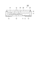
図1(a)は、本発明の実施形態1に係る電子デバイスの外観を示す平面図であり、図1(b)は、蓋体を外し電子デバイスの内部を示す平面図である。また、図2は、電子デバイスの内部を示す断面図であり、図1(a)の電子デバイスにおけるA−A線に沿う断面を表している。電子デバイス100は、図1(a)の平面図に示すように、平面視した外観が長方形をなしていて、パッケージ10と、蓋体20と、パッケージ10に蓋体20を接合しているシームリング30と、を備えている。この場合、シームリング30は、パッケージ10が有するメタライズ部であり、蓋体20は、メタライズ部であるシームリング30に、平面視で重なるように、設けられている封止孔(孔部)25を有している。この場合、封止孔25は、一箇所に設けられていて、円形の貫通孔である。
FIG. 1A is a plan view showing the appearance of an electronic device according to Embodiment 1 of the present invention, and FIG. 1B is a plan view showing the inside of the electronic device with the lid removed. Moreover, FIG. 2 is sectional drawing which shows the inside of an electronic device, and represents the cross section in alignment with the AA in the electronic device of Fig.1 (a). As shown in the plan view of FIG. 1A, the
また、図1(b)または図2に示す電子デバイス100のパッケージ10は、絶縁材料である酸化アルミニウム質のセラミックグリーンシートで成形され、成形後に焼結処理により形成されている。このパッケージ10は、その内側に形成され蓋体20の側が開放されている内部空間Sと、内部空間Sに設けられている段部11と、段部11に設けられている電極部12と、外面側に設けられ電極部12と電気的に接続している実装端子13と、を有している。そして、内部空間Sには、電極部12に導電性接着剤14を介して固定されている、電子部品としての水晶振動片40が収容されている。この場合、導電性接着剤14は、接合力を発揮する接着剤成分としてのエポキシ系合成樹脂剤に、銀(Ag)の微細粒子を含有させたものであり、電極部12および実装端子13は、金(Au)メッキで形成されている。
The
また、蓋体20は、パッケージ10との熱膨張率が近似し接合の容易な材料を用いることが好ましく、例えばパッケージ10と同じセラミック材、または鉄(Fe)とコバルト(Co)の合金であるコバール、ステンレス鋼等の金属を用いることができ、電子デバイス100ではコバールを用いている。そして、ここではコバールの表面にニッケル(Ni)メッキ(不図示)を施している。シームリング30は、予めパッケージ10に接合され蓋体20をパッケージ10に接合しやすくするためのものであり、電子デバイス100ではコバールを用いている。シームリング30およびシームリング30が接合されているパッケージ面は、平面視で均一な幅をなしていて、パッケージ面が平面視幅W1であり、シームリング30の平面視幅は、パッケージ面の平面視幅W1より狭くなっている。
The
このような構成の電子デバイス100は、蓋体20がパッケージ10のシームリング30に接合された後、封止孔25から内部空間Sの空気が抜かれ、さらに封止孔25がシームリング30に接合されて封止されることにより、内部空間Sが減圧状態で確実に封止されている。この接合にかかる製造方法については、図4を参照して、フローチャートに基づき後述する。
In the
なお、導電性接着剤14は、合成樹脂剤がエポキシ系であることに限定されず、シリコーン系、ポリイミド系導電性接着剤等を利用することができ、微細粒子は、銀(Ag)以外の金属であっても良く、金属バンプであっても良い。電極部12および実装端子13は、ニッケル(Ni)メッキ等でも良い。
In addition, the
次に、パッケージ10の内部空間Sに収容される、電子部品としての水晶振動片40について説明する。電子部品の一例である水晶振動片40は、基部41と、基部41から互いに平行に延出する一対の振動腕42と、一対の振動腕42の蓋体20と対向する面および当該面の反対側の面に形成され、振動腕42の延出方向に沿って形成されている長溝43と、基部41から振動腕42の延出方向と平面視で直交する方向へそれぞれ延び、さらに振動腕42と平行する方向へ曲がって延出している一対の支持用アーム45と、を備えている。そして、水晶振動片40は、長溝43の内部および各振動腕42における長溝43の形成されていない面に対になって形成されている励振電極44と、それぞれの励振電極44から支持用アーム45のいずれかへ引き回されている引き出し電極44aと、を備えている。
Next, the
なお、水晶振動片40における基部41、音叉状の振動腕42、各振動腕42に設けられる長溝43は、例えば水晶ウエハなどの材料をフッ酸溶液などでウエットエッチングすることにより精密に形成することができる。また、励振電極44および引き出し電極44aは、蒸着またはスパッタリングにより、水晶との密着性が良好なクロム(Cr)を下地層として成膜し、その上に電気抵抗が低く酸化し難い金(Au)によって電極層を成膜し、その後フォトリソグラフィを用いてパターニングすることにより形成されている。
The
このような構成を備えている電子デバイス100を実装基板などに実装した場合に、外部からの駆動電圧が実装端子13から電極部12を介して水晶振動片40の支持用アーム45の引き出し電極44aに伝えられ、さらに励振電極44に伝えられることにより、振動腕42が互いに異なる方向へ屈曲して振動する。この場合、水晶振動片40は、各振動腕42に設けられた長溝43によって、剛性が小さくなって振動しやすくなっているため、振動腕42が効率よく振動して、良好な振動特性を有することができる。この水晶振動片40は、いわゆる音叉型振動片である。
When the
なお、電子デバイス100における電子部品は、水晶振動片40に限定されるものではなく、音叉型振動片以外の種々の形態のものであっても良く、さらに、材質が水晶以外のタンタル酸リチウム(LiTaO3)、四ホウ酸リチウム(Li2B4O7)、ニオブ酸リチウム(LiNbO3)、チタン酸ジルコン酸鉛(PZT)、酸化亜鉛(ZnO)、窒化アルミニウム(AlN)などの他の圧電材料や、圧電材が巻装されている等の構成を有するシリコンやゲルマニウム等の非圧電材料等であっても良い。
The electronic component in the
次に、電子デバイス100において、パッケージ10の内部空間Sを封止するための構成について説明する。図3(a)は、蓋体の封止孔の加工例を示す断面図であり、図3(b)は、パッケージと蓋体および封止孔との接合構成を示す断面図である。ここでの説明において、蓋体20単体においては封止孔25aとし、封止後(図1および図2)においては封止孔25として区別する。封止孔25aは、プレス抜き加工やドリル加工等によって蓋体20に設けることができるが、ここでは図3(a)に示すように、プレス抜き加工で孔径d1の円形に形成されている。従って、封止孔25aは、プレス抜き方向Pにおける抜き加工開始側の面である蓋面20aの側が孔内面方向へ押し込まれてダレ込んだ形状となっている。また、蓋面20aと反対側の面には、孔外部方向へバリが生じている。このバリは、バレル処理等を行えば、容易に除去することができるが、パッケージ10と蓋体20との接合では、蓋面20aをパッケージ10の側、即ちシームリング30に載置することが望ましい。これにより、蓋体20は、シームリング30に対して接合等の支障となる隙間等を生じることなく、載置されることになる。なお、封止孔25aは、円形の貫通孔に限らず、楕円形、矩形、多角形等であっても良く、また一箇所でなく複数個所に設けられていても良い。
Next, a configuration for sealing the internal space S of the
シームリング30に蓋体20が載置されて、シーム溶接およびエネルギービーム照射により接合されると、図3(b)に示すような接合状態となる。ここで、蓋体20の外周部20bは、シームリング30の外周部30aより小さい相似形状をなしている。そして、シームリング30と蓋体20との接合は、まず、蓋体20の外周部20bとシームリング30とがシーム溶接され、蓋体20表面のニッケル(Ni)メッキを含め互いに溶融することにより接合し、外周部20bとシームリング30との境界部に第1接合部50aが形成される。さらに、封止孔25aに対して孔径d1より大きな照射径d2のエネルギービームBを照射することにより、封止孔25aの内面が溶融して同じく溶融したシームリング30と接合し、封止孔25aとシームリング30との境界部分に第2接合部50bが形成される。接合後の封止孔25は、接合前の封止孔25aより大きな径、即ち照射径d2に近い径となっている。蓋体20の封止孔25とシームリング30の溶融部分は、封止孔25の孔内面側に広がっていて、断面形状が略三角形状のフィレット状部22を形成している。このフィレット状部22を形成することにより、封止孔25とシームリング30とを封止するための第2接合部50bが強固に形成される。これら第1接合部50aおよび第2接合部50bにより、内部空間Sは、パッケージ10および蓋体20の外部側と遮断されて、確実に封止された状態となっている。ここでいうエネルギービームBは、電子ビームやレーザー等を含むものを指す。
When the
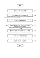
このような接合構成を備えている電子デバイス100の製造方法について、以下に説明する。図4は、電子デバイスの製造方法を示すフローチャートである。まず、工程S1において、蓋体とパッケージとを用意する。ここでは、プレス加工で形成された封止孔25aを有する蓋体20と、電極部12、実装端子13、シームリング30および水晶振動片40を有するパッケージ10と、を別々に製造して準備しておく。つまり、工程S1は、準備工程に該当する。準備後、工程S2へ進む。
A method for manufacturing the
工程S2において、電子部品をパッケージに搭載する。つまり、パッケージ10の内部空間Sに電子部品である水晶振動片40を振動可能な状態で固定して搭載する。工程S2は、搭載工程に該当する。搭載後工程S3へ進む。
In step S2, an electronic component is mounted on a package. That is, the quartz
工程S3において、パッケージに蓋体を載置する。より具体的には、パッケージ10のシームリング30に蓋体20の蓋面20aの側を載置する。この時、既述したように、蓋体20の外周部20bは、シームリング30の外周部30aより小さい設定であり、双方の間が全周に渡りほぼ一定の幅となるように配置され、蓋体20とシームリング30とは、ほぼ密着した状態で配置される。配置後、工程S4へ進む。
In step S3, a lid is placed on the package. More specifically, the
工程S4において、蓋体の封止孔とパッケージのメタライズ部とが平面視で重なっているか否かを判断する。この場合のメタライズ部は、シームリング30を指している。また、判断は、工程S3で載置作業をしたロボットによる画像認識あるいは作業者等により行われる。パッケージ10と蓋体20とが、平面視で重なっているように配置されていれば、蓋体20の封止孔25aは、シームリング30との接合が可能な配置となっている。この配置がキーポイントであり、この配置状態を工程S4で確認し判断する。工程S4は、工程S3と共に載置工程に該当する。確認結果で、封止孔25aとシームリング30とが重なっていれば、工程S5へ進み、一方、封止孔25aとシームリング30とが重なっていなければ、工程S3へ戻る。
In step S4, it is determined whether or not the sealing hole of the lid and the metallized portion of the package overlap in plan view. In this case, the metallized portion indicates the
そして、封止孔25aとシームリング30とが重なっていれば、工程S5において、蓋体の外周部とメタライズ部とをシーム溶接する。これは、図3(b)に示すように、蓋体20の外周部20bとメタライズ部であるシームリング30とを溶融して第1接合部50aを形成し、蓋体20の外周部20bの全周を封止する工程である。これにより、内部空間Sは、封止孔25aおよび蓋体20の蓋面20aとシームリング30との間を介してのみ、外部側と連通している状態である。この場合、蓋体20およびシームリング30を構成するコバールの融点は約1450℃の高温であり、蓋体20とシームリング30との境界部を局部的且つ迅速にシーム溶接することが望ましい。工程S5は、第1接合工程に該当する。溶接後、工程S6へ進む。
If the sealing
工程S6において、パッケージの内部空間を減圧する。ここでは、第1接合部50aを形成して接合したパッケージ10と蓋体20とを真空に近い減圧雰囲気の中に置いて、内部空間Sを減圧する。つまり、減圧雰囲気下において、内部空間Sの空気は、封止孔25aを通じてのみ、減圧状態になっている外部側へ排出される。これにより、内部空間Sは、外部側と同じ減圧雰囲気となる。なお、内部空間Sは、減圧雰囲気とするだけでなく、不活性ガス雰囲気にして密閉・封止されていても良い。この場合、減圧雰囲気および不活性雰囲気の内部空間Sは、減圧されて封止されていて、工程S6は、内部空間Sを減圧する工程である。減圧後、工程S7へ進む。
In step S6, the internal space of the package is depressurized. Here, the internal space S is decompressed by placing the
工程S7において、封止孔へエネルギービームを照射する。具体的には、図3(b)に示すように、封止孔25aへエネルギービームBを照射して封止孔25a内面およびシームリング30を溶融する。この溶融により形成された封止孔25におけるフィレット状部22、およびシームリング30との境界部である第2接合部50bとにより、封止孔25とシームリング30とが確実に封止される。これにより、水晶振動片40を収容している内部空間Sは、外部側とは完全に封止される。また、水晶振動片40は、内部空間Sにおける一定の減圧雰囲気のもとで、安定した振動をすることが可能となり、電子デバイス100のタイミングデバイス機能の安定化に貢献できる。工程S7は、第2接合工程に該当する。以上で、電子デバイスの製造方法に関するフローが終了し、電子デバイス100が完成する。完成した電子デバイス100には封止された封止孔25が残るので、電子デバイスの搭載向き判別などのマーキングとしての効果もある。
(実施形態2)
In step S7, the sealing hole is irradiated with an energy beam. Specifically, as shown in FIG. 3B, the sealing
(Embodiment 2)
次に、電子デバイスの製造方法により製造された電子デバイスの他の好適例について説明する。図5は、実施形態2に係る電子デバイスのパッケージと蓋体および封止孔との接合構成を示す断面図である。電子デバイス200は、パッケージ10と蓋体20および封止孔25aとの接合構成のみが実施形態1の電子デバイス100とは異なっていて、他は電子デバイス100と同様な構成になっている。電子デバイス200において、パッケージ10にはシームリング30が接合されていて、蓋体20のシームリング30に対向して載置される面側である蓋面20aには、銀(Ag)ロウ28が全面に配置されている。
Next, another preferred example of the electronic device manufactured by the electronic device manufacturing method will be described. FIG. 5 is a cross-sectional view illustrating a bonding configuration of the electronic device package, the lid, and the sealing hole according to the second embodiment. The
そして、蓋体20は、シームリング30に載置されて、シーム溶接およびエネルギービーム照射により接合されると、図5に示すような接合状態となる。ここで、蓋体20の外周部20bは、シームリング30の外周部30aより小さい相似形状をなしている。シームリング30と蓋体20との接合は、まず、蓋体20の外周部20b側の蓋面20aとシームリング30との間がシーム溶接されて銀(Ag)ロウ28が溶融することにより、蓋体20とシームリング30とがニッケル(Ni)メッキを介して接合される。この場合、銀(Ag)ロウ28の溶融部分が第1接合部60aである。さらに、封止孔25aに対してエネルギービームB(図3(b)参照)を照射することにより、封止孔25a近傍の銀(Ag)ロウ28が溶融して蓋体20とシームリング30とがニッケル(Ni)メッキを介して接合される。この場合、銀(Ag)ロウ28の溶融部分が第2接合部60bである。
When the
このように、銀(Ag)ロウ28を用いて蓋体20とシームリング30とを接合することにより、実施形態1における接合よりも低い温度、即ち銀(Ag)ロウ28の融点である700℃程度で接合することができ、内部空間Sは、パッケージ10および蓋体20の外部側と遮断されて、確実に封止された状態となっている。これにより、電子デバイス200は、より低温度で加工ができるため接合が容易になると共に、パッケージ10や蓋体20や水晶振動片40等に対する熱影響も抑制することができる。
Thus, by joining the
なお、蓋体20とシームリング30との接合には、銀(Ag)ロウ28以外に例えば金(Au)/錫(Sn)合金ロウ等を用いることも可能である。金(Au)/錫(Sn)合金ロウの融点は、銀(Ag)ロウ28より低い300℃程度であって、接合温度を下げることが可能である。これにより、封止孔25aを含め蓋体20とシームリング30との接合がより容易になって、パッケージ10や蓋体20や水晶振動片40等に対する熱影響がより抑制され、さらに、銀(Ag)ロウ28等に比べて接合部分の耐食性の向上も図れる。
(実施形態3)
In addition to the silver (Ag) braze 28, for example, a gold (Au) / tin (Sn) alloy braze or the like can be used for joining the
(Embodiment 3)
次に、電子デバイスの製造方法により製造された電子デバイスの他の好適例について説明する。図6(a)は、実施形態3に係る電子デバイスの構成を示す平面図、図6(b)は、パッケージと蓋体および封止孔との接合構成を示す断面図である。図6(a)は、蓋体20を外して、内部空間Sに収容されている水晶振動片40を示している。電子デバイス300は、内部空間Sの平面視形状、パッケージ10と蓋体20および封止孔25との接合構成と、が実施形態1の電子デバイス100または実施形態2の電子デバイス200とは異なっていて、他は電子デバイス100,200と同様な構成になっている。
Next, another preferred example of the electronic device manufactured by the electronic device manufacturing method will be described. 6A is a plan view showing the configuration of the electronic device according to the third embodiment, and FIG. 6B is a cross-sectional view showing the bonding configuration of the package, the lid, and the sealing hole. FIG. 6A shows the
図6(a)に示すように、電子デバイス300は、パッケージ10の内部空間Sが長方形をなす一隅において内部側に狭まっている。つまり、パッケージ10の蓋体20を載置する面は平面視幅W1であるが、封止孔25が配置される位置である一隅では平面視幅W2となっていて、平面視幅W2は平面視幅W1より大きい。この平面視幅W2を形成する位置は、水晶振動片40の振動を妨げなければ、隅部以外のいずれの位置であっても良い。
As shown in FIG. 6A, the
そして、図6(b)に示すように、パッケージ10の蓋体20が載置される面には、メタライズ部としての金属膜15が形成されている。金属膜15は、この場合ニッケル(Ni)であり蒸着によって形成されている。従って、パッケージ10に載置される蓋体20が位置ズレを生じていたとしても、封止孔25が、平面視幅W2の広範なメタライズ部である金属膜15に対しては平面視で重なるように配置されることになる。即ち、蓋体20をパッケージ10に載置する際の位置ズレの許容範囲が広く設定できる。
And as shown in FIG.6 (b), the
このような金属膜15と蓋体20とは、シーム溶接およびエネルギービーム照射により接合されると、図6(b)に示すような接合状態となる。ここで、パッケージ10と蓋体20との接合は、まず、蓋体20の外周部20bの側とパッケージ10の金属膜15とがシーム溶接され、互いに溶融することにより接合し、外周部20bと金属膜15とで第1接合部70aが形成される。さらに、エネルギービームB(図3(b)参照)を照射することにより、封止孔25にフィレット状部22が形成され、フィレット状部22と金属膜15とが接合して第2接合部70bが形成される。これら第1接合部70aおよび第2接合部70bにより、内部空間Sは、パッケージ10および蓋体20の外部側と遮断されて、確実に封止された状態を維持することができる。また、封止孔25位置でのパッケージ10の平面視幅W2が大きく設定してあるため、シーム溶接およびエネルギービーム照射における熱が吸収されやすくなり、パッケージ10や蓋体20や水晶振動片40等に対する熱影響がより一層抑制される。
When such a
なお、電子デバイス300は、金属膜15をメタライズ部としてパッケージ10と蓋体20とを接合しているが、図3(b)に示すようなシームリング30を用いる方法や、図5に示すような銀(Ag)ロウ28等を用いる方法によって、パッケージ10と蓋体20とを接合することも可能である。また、平面視幅W2は、内部空間Sの内部側に向かって広がっているが、外部側へ向かって広がっていても良く、さらに内外両側へ広がっている構成であっても良い。
(電子機器)
In the
(Electronics)
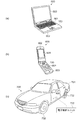
次に、本発明の電子デバイス100,200,300を搭載した電子機器および移動体について説明する。図7(a)は、電子デバイスを搭載したパーソナルコンピューターを示す斜視図、図7(b)は、電子デバイスを搭載した携帯電話を示す斜視図、図7(c)は、電子デバイスを搭載した移動体を示す斜視図である。
Next, an electronic apparatus and a moving body equipped with the
図7(a)に示すパーソナルコンピューター500は、電子デバイス100が一例として搭載されていて、さらに、キーボード501と、キーボード501を備えた本体部502と、表示ユニット503と、により構成されている。表示ユニット503は、本体部502に対しヒンジ構造部を介して回動可能に支持されている。このような構成のパーソナルコンピューター500の電子デバイス100には、水晶振動片40がタイミングデバイスとして内蔵されていて、パーソナルコンピューター500の携帯時の振動や衝撃等にも耐えて、パーソナルコンピューター500の性能維持に貢献している。
A
また、図7(b)に示す携帯電話機600は、電子デバイス100が一例として搭載されていて、さらに、複数の操作ボタン601と、受話口602と、送話口603と、アンテナ(不図示)とを備えている。操作ボタン601と受話口602との間には、表示部604が配置されている。このような構成の携帯電話機600の電子デバイス100には、水晶振動片40がタイミングデバイスとして内蔵されていて、携帯電話機600の携帯時の振動や衝撃等にも耐えて、携帯電話機600の性能維持に貢献している。
7B includes the
そして、図7(c)に示す移動体700は、例えば自動車等が該当する。この場合、自動車である移動体700には、電子部品である水晶振動片40を備え加速度や傾斜等を検出できるように構成されている、電子デバイス400が搭載されている。移動体700において、電子デバイス400は、車体701に搭載されている電子制御ユニット(ECU:electronic control unit)703に内蔵されている。電子制御ユニット703は、電子デバイス400が車体701の加速度や傾斜等を検出することにより、移動状態や姿勢等を把握し、タイヤ702等の制御を的確に行うことができる。これにより、移動体700は、安全で安定した走行をすることが可能である。
And the
なお、電子デバイス100,200,300および電子デバイス400は、既述したパーソナルコンピューター500、携帯電話機600および移動体700に搭載される以外に、その機能に応じて、例えば、ディジタルスチルカメラ、インクジェット式吐出装置、テレビ、ビデオカメラ、ビデオレコーダ、カーナビゲーション装置、電子手帳、電子辞書、電卓、電子ゲーム機器、ワークステーション、防犯用テレビモニター、電子双眼鏡、POS端末、医療機器(例えば電子体温計、血圧計、血糖計、心電図計測装置、超音波診断装置、電子内視鏡)、魚群探知機、各種測定機器・計器類(例えば、車両、航空機、船舶の計器類)、フライトシミュレーター等にも搭載可能である。
The
10…パッケージ、15…メタライズ部としての金属膜、20…蓋体、20a…抜き加工開始側の面としての蓋面、20b…外周部、22…フィレット状部、25…孔部としての封止孔、25a…(封止される前の)封止孔、30…メタライズ部としてのシームリング、40…電子部品としての水晶振動片、50a…第1接合部、50b…第2接合部、100…電子デバイス、200,300,400…電子デバイス、500…電子機器としてのパーソナルコンピューター、600…電子機器としての携帯電話、700…移動体、B…エネルギービーム、d1…(封止孔25aの)孔径、d2…照射径、W1,W2…平面視幅。
DESCRIPTION OF
Claims (9)
前記電子部品を前記パッケージに搭載する搭載工程と、
前記封止孔と前記メタライズ部とが平面視で重なるように前記蓋体を前記パッケージに載置する載置工程と、
前記蓋体の外周部と前記パッケージとをシーム溶接する第1接合工程と、
エネルギービームを照射して前記封止孔と前記メタライズ部とを接合し前記封止孔と前記内部空間とを封止する第2接合工程と、
を含むことを特徴とする電子デバイスの製造方法。 A preparatory step of preparing a lid body having a sealing hole, a package for forming an internal space together with the lid body having a metallized portion, and an electronic component;
A mounting step of mounting the electronic component on the package;
A placing step of placing the lid on the package such that the sealing hole and the metallized portion overlap in plan view;
A first joining step of seam welding the outer periphery of the lid and the package;
A second bonding step of irradiating an energy beam to bond the sealing hole and the metallized portion to seal the sealing hole and the internal space;
The manufacturing method of the electronic device characterized by the above-mentioned.
前記第2接合工程では、前記蓋体の前記メタライズ部に載置される面側に前記一方の面を配置し、前記封止孔と前記メタライズ部とを前記金属ロウによって接合する、ことを特徴とする請求項1に記載の電子デバイスの製造方法。 A metal solder is disposed on one surface of the lid,
In the second joining step, the one surface is disposed on a surface side of the lid placed on the metallized portion, and the sealing hole and the metallized portion are joined by the metal brazing. The method for manufacturing an electronic device according to claim 1.
前記載置工程では、前記蓋体の抜き加工開始側の面が前記パッケージに載置される、ことを特徴とする請求項1から5のいずれか一項に記載の電子デバイスの製造方法。 The sealing hole is formed by press punching,
6. The method of manufacturing an electronic device according to claim 1, wherein, in the placing step, a surface on the punching start side of the lid is placed on the package. 6.
Priority Applications (3)
| Application Number | Priority Date | Filing Date | Title |
|---|---|---|---|
| JP2012175752A JP2014036081A (en) | 2012-08-08 | 2012-08-08 | Method for manufacturing electronic device, electronic device, electronic equipment, and movable body |
| CN201310336702.2A CN103579014A (en) | 2012-08-08 | 2013-08-05 | Method of manufacturing electronic device, electronic device, electronic apparatus, and mobile object |
| US13/959,877 US20140043779A1 (en) | 2012-08-08 | 2013-08-06 | Method of manufacturing electronic device, electronic device, electronic apparatus, and mobile object |
Applications Claiming Priority (1)
| Application Number | Priority Date | Filing Date | Title |
|---|---|---|---|
| JP2012175752A JP2014036081A (en) | 2012-08-08 | 2012-08-08 | Method for manufacturing electronic device, electronic device, electronic equipment, and movable body |
Publications (2)
| Publication Number | Publication Date |
|---|---|
| JP2014036081A true JP2014036081A (en) | 2014-02-24 |
| JP2014036081A5 JP2014036081A5 (en) | 2015-09-10 |
Family
ID=50050520
Family Applications (1)
| Application Number | Title | Priority Date | Filing Date |
|---|---|---|---|
| JP2012175752A Withdrawn JP2014036081A (en) | 2012-08-08 | 2012-08-08 | Method for manufacturing electronic device, electronic device, electronic equipment, and movable body |
Country Status (3)
| Country | Link |
|---|---|
| US (1) | US20140043779A1 (en) |
| JP (1) | JP2014036081A (en) |
| CN (1) | CN103579014A (en) |
Cited By (1)
| Publication number | Priority date | Publication date | Assignee | Title |
|---|---|---|---|---|
| WO2019059338A1 (en) * | 2017-09-22 | 2019-03-28 | 株式会社村田製作所 | Piezoelectric transducer and method for producing piezoelectric transducer |
Families Citing this family (3)
| Publication number | Priority date | Publication date | Assignee | Title |
|---|---|---|---|---|
| JP6167494B2 (en) * | 2012-09-26 | 2017-07-26 | セイコーエプソン株式会社 | Electronic device container manufacturing method, electronic device manufacturing method, electronic device, electronic apparatus, and mobile device |
| CN106028649B (en) * | 2016-07-28 | 2019-02-12 | Oppo广东移动通信有限公司 | The circuit board of mobile terminal and mobile terminal with it |
| DE102017125140B4 (en) * | 2017-10-26 | 2021-06-10 | Infineon Technologies Ag | Method for producing a hermetically sealed housing with a semiconductor component |
Citations (7)
| Publication number | Priority date | Publication date | Assignee | Title |
|---|---|---|---|---|
| JPS5232269A (en) * | 1975-09-05 | 1977-03-11 | Matsushita Electric Ind Co Ltd | Hermetic sealing method of semiconductor devices |
| JPH10189795A (en) * | 1996-12-19 | 1998-07-21 | Murata Mfg Co Ltd | Element package structure and manufacture thereof |
| JP2004266239A (en) * | 2003-01-10 | 2004-09-24 | Seiko Epson Corp | Piezoelectric device |
| JP2004289238A (en) * | 2003-03-19 | 2004-10-14 | Seiko Epson Corp | Package for piezoelectric device, piezoelectric device and their manufacturing method, mobile telephone employing the piezoelectric device, and electronic equipment employing the piezoelectric device |
| JP2004320150A (en) * | 2003-04-11 | 2004-11-11 | Seiko Epson Corp | Piezoelectric device, package therefor, method of manufacturing the same |
| WO2010010721A1 (en) * | 2008-07-25 | 2010-01-28 | 日本電気株式会社 | Encapsulating package, printed circuit board, electronic device and method for manufacturing encapsulating package |
| JP2010119141A (en) * | 2010-02-22 | 2010-05-27 | Kyocera Corp | Device apparatus |
Family Cites Families (3)
| Publication number | Priority date | Publication date | Assignee | Title |
|---|---|---|---|---|
| US5041695A (en) * | 1989-06-01 | 1991-08-20 | Westinghouse Electric Corp. | Co-fired ceramic package for a power circuit |
| US20040241906A1 (en) * | 2003-05-28 | 2004-12-02 | Vincent Chan | Integrated circuit package and method for making same that employs under bump metalization layer |
| JP5007494B2 (en) * | 2005-07-04 | 2012-08-22 | セイコーエプソン株式会社 | Manufacturing method of electronic device |
-
2012
- 2012-08-08 JP JP2012175752A patent/JP2014036081A/en not_active Withdrawn
-
2013
- 2013-08-05 CN CN201310336702.2A patent/CN103579014A/en active Pending
- 2013-08-06 US US13/959,877 patent/US20140043779A1/en not_active Abandoned
Patent Citations (7)
| Publication number | Priority date | Publication date | Assignee | Title |
|---|---|---|---|---|
| JPS5232269A (en) * | 1975-09-05 | 1977-03-11 | Matsushita Electric Ind Co Ltd | Hermetic sealing method of semiconductor devices |
| JPH10189795A (en) * | 1996-12-19 | 1998-07-21 | Murata Mfg Co Ltd | Element package structure and manufacture thereof |
| JP2004266239A (en) * | 2003-01-10 | 2004-09-24 | Seiko Epson Corp | Piezoelectric device |
| JP2004289238A (en) * | 2003-03-19 | 2004-10-14 | Seiko Epson Corp | Package for piezoelectric device, piezoelectric device and their manufacturing method, mobile telephone employing the piezoelectric device, and electronic equipment employing the piezoelectric device |
| JP2004320150A (en) * | 2003-04-11 | 2004-11-11 | Seiko Epson Corp | Piezoelectric device, package therefor, method of manufacturing the same |
| WO2010010721A1 (en) * | 2008-07-25 | 2010-01-28 | 日本電気株式会社 | Encapsulating package, printed circuit board, electronic device and method for manufacturing encapsulating package |
| JP2010119141A (en) * | 2010-02-22 | 2010-05-27 | Kyocera Corp | Device apparatus |
Cited By (3)
| Publication number | Priority date | Publication date | Assignee | Title |
|---|---|---|---|---|
| WO2019059338A1 (en) * | 2017-09-22 | 2019-03-28 | 株式会社村田製作所 | Piezoelectric transducer and method for producing piezoelectric transducer |
| JPWO2019059338A1 (en) * | 2017-09-22 | 2020-11-12 | 株式会社村田製作所 | Piezoelectric oscillator and manufacturing method of piezoelectric oscillator |
| US11309864B2 (en) | 2017-09-22 | 2022-04-19 | Murata Manufacturing Co., Ltd. | Piezoelectric resonator unit and method for manufacturing the piezoelectric resonator unit |
Also Published As
| Publication number | Publication date |
|---|---|
| US20140043779A1 (en) | 2014-02-13 |
| CN103579014A (en) | 2014-02-12 |
Similar Documents
| Publication | Publication Date | Title |
|---|---|---|
| JP6167494B2 (en) | Electronic device container manufacturing method, electronic device manufacturing method, electronic device, electronic apparatus, and mobile device | |
| JP4462332B2 (en) | Electronic components | |
| JP2008218811A (en) | Function element package | |
| US9509276B2 (en) | Acoustic wave device and method of fabricating the same | |
| WO2008018222A1 (en) | Piezoelectric vibration device | |
| JP2014036081A (en) | Method for manufacturing electronic device, electronic device, electronic equipment, and movable body | |
| JP2007059736A (en) | Piezoelectric vibrator package, its manufacturing method, and physical value sensor | |
| JP2013046167A (en) | Vibration device and manufacturing method of vibration device | |
| JP2014197575A (en) | Package, electronic device, method of manufacturing electronic device, electronic apparatus, and mobile body | |
| JP5505189B2 (en) | Vibration device and electronic equipment | |
| JP2007251239A (en) | Piezoelectric device and manufacturing method thereof | |
| JP2005143042A (en) | Piezoelectric device | |
| JP5251224B2 (en) | Method for manufacturing piezoelectric vibration device and piezoelectric vibration device | |
| JP2015094614A (en) | Lid body, package, electronic apparatus, movable body, and manufacturing method of package | |
| JP2006086585A (en) | Surface-mounted piezoelectric resonating device | |
| JP2007073713A (en) | Package for piezo-electric device | |
| JP3922570B2 (en) | Piezoelectric device and package for piezoelectric device, method for manufacturing piezoelectric device, mobile phone device using piezoelectric device, and electronic equipment using piezoelectric device | |
| JP5196121B2 (en) | device | |
| JP2014110370A (en) | Base substrate, mounting structure, module, electronic equipment, and mobile object | |
| JP2003069368A (en) | Method for joining piezoelectric device and piezoelectric vibration chip, mobile phone employing the piezoelectric device and electronic device employing the piezoelectric device | |
| JP2017212612A (en) | Piezoelectric device and manufacturing method of the same | |
| JP2001274649A (en) | Method for air-tightly sealing quartz vibration device | |
| JP2009117869A (en) | Method of manufacturing functional element package | |
| JP2007318209A (en) | Surface mounted piezoelectric vibrating device, and manufacturing method thereof | |
| JP4599145B2 (en) | Piezoelectric diaphragm |
Legal Events
| Date | Code | Title | Description |
|---|---|---|---|
| RD04 | Notification of resignation of power of attorney |
Free format text: JAPANESE INTERMEDIATE CODE: A7424 Effective date: 20150108 |
|
| A521 | Request for written amendment filed |
Free format text: JAPANESE INTERMEDIATE CODE: A523 Effective date: 20150722 |
|
| A621 | Written request for application examination |
Free format text: JAPANESE INTERMEDIATE CODE: A621 Effective date: 20150722 |
|
| RD04 | Notification of resignation of power of attorney |
Free format text: JAPANESE INTERMEDIATE CODE: A7424 Effective date: 20160610 |
|
| RD03 | Notification of appointment of power of attorney |
Free format text: JAPANESE INTERMEDIATE CODE: A7423 Effective date: 20160624 |
|
| A977 | Report on retrieval |
Free format text: JAPANESE INTERMEDIATE CODE: A971007 Effective date: 20160725 |
|
| A131 | Notification of reasons for refusal |
Free format text: JAPANESE INTERMEDIATE CODE: A131 Effective date: 20160802 |
|
| A761 | Written withdrawal of application |
Free format text: JAPANESE INTERMEDIATE CODE: A761 Effective date: 20160923 |