JP2013513235A - Oxygen doping for non-carbon radical component CVD films - Google Patents
Oxygen doping for non-carbon radical component CVD films Download PDFInfo
- Publication number
- JP2013513235A JP2013513235A JP2012542040A JP2012542040A JP2013513235A JP 2013513235 A JP2013513235 A JP 2013513235A JP 2012542040 A JP2012542040 A JP 2012542040A JP 2012542040 A JP2012542040 A JP 2012542040A JP 2013513235 A JP2013513235 A JP 2013513235A
- Authority
- JP
- Japan
- Prior art keywords
- oxygen
- precursor
- plasma
- silicon
- radical
- Prior art date
- Legal status (The legal status is an assumption and is not a legal conclusion. Google has not performed a legal analysis and makes no representation as to the accuracy of the status listed.)
- Pending
Links
Images


Classifications
-
- H—ELECTRICITY
- H01—ELECTRIC ELEMENTS
- H01L—SEMICONDUCTOR DEVICES NOT COVERED BY CLASS H10
- H01L21/00—Processes or apparatus adapted for the manufacture or treatment of semiconductor or solid state devices or of parts thereof
- H01L21/02—Manufacture or treatment of semiconductor devices or of parts thereof
- H01L21/02104—Forming layers
- H01L21/02107—Forming insulating materials on a substrate
- H01L21/02225—Forming insulating materials on a substrate characterised by the process for the formation of the insulating layer
- H01L21/0226—Forming insulating materials on a substrate characterised by the process for the formation of the insulating layer formation by a deposition process
- H01L21/02263—Forming insulating materials on a substrate characterised by the process for the formation of the insulating layer formation by a deposition process deposition from the gas or vapour phase
- H01L21/02271—Forming insulating materials on a substrate characterised by the process for the formation of the insulating layer formation by a deposition process deposition from the gas or vapour phase deposition by decomposition or reaction of gaseous or vapour phase compounds, i.e. chemical vapour deposition
- H01L21/02274—Forming insulating materials on a substrate characterised by the process for the formation of the insulating layer formation by a deposition process deposition from the gas or vapour phase deposition by decomposition or reaction of gaseous or vapour phase compounds, i.e. chemical vapour deposition in the presence of a plasma [PECVD]
-
- C—CHEMISTRY; METALLURGY
- C23—COATING METALLIC MATERIAL; COATING MATERIAL WITH METALLIC MATERIAL; CHEMICAL SURFACE TREATMENT; DIFFUSION TREATMENT OF METALLIC MATERIAL; COATING BY VACUUM EVAPORATION, BY SPUTTERING, BY ION IMPLANTATION OR BY CHEMICAL VAPOUR DEPOSITION, IN GENERAL; INHIBITING CORROSION OF METALLIC MATERIAL OR INCRUSTATION IN GENERAL
- C23C—COATING METALLIC MATERIAL; COATING MATERIAL WITH METALLIC MATERIAL; SURFACE TREATMENT OF METALLIC MATERIAL BY DIFFUSION INTO THE SURFACE, BY CHEMICAL CONVERSION OR SUBSTITUTION; COATING BY VACUUM EVAPORATION, BY SPUTTERING, BY ION IMPLANTATION OR BY CHEMICAL VAPOUR DEPOSITION, IN GENERAL
- C23C16/00—Chemical coating by decomposition of gaseous compounds, without leaving reaction products of surface material in the coating, i.e. chemical vapour deposition [CVD] processes
- C23C16/22—Chemical coating by decomposition of gaseous compounds, without leaving reaction products of surface material in the coating, i.e. chemical vapour deposition [CVD] processes characterised by the deposition of inorganic material, other than metallic material
- C23C16/30—Deposition of compounds, mixtures or solid solutions, e.g. borides, carbides, nitrides
- C23C16/308—Oxynitrides
-
- C—CHEMISTRY; METALLURGY
- C23—COATING METALLIC MATERIAL; COATING MATERIAL WITH METALLIC MATERIAL; CHEMICAL SURFACE TREATMENT; DIFFUSION TREATMENT OF METALLIC MATERIAL; COATING BY VACUUM EVAPORATION, BY SPUTTERING, BY ION IMPLANTATION OR BY CHEMICAL VAPOUR DEPOSITION, IN GENERAL; INHIBITING CORROSION OF METALLIC MATERIAL OR INCRUSTATION IN GENERAL
- C23C—COATING METALLIC MATERIAL; COATING MATERIAL WITH METALLIC MATERIAL; SURFACE TREATMENT OF METALLIC MATERIAL BY DIFFUSION INTO THE SURFACE, BY CHEMICAL CONVERSION OR SUBSTITUTION; COATING BY VACUUM EVAPORATION, BY SPUTTERING, BY ION IMPLANTATION OR BY CHEMICAL VAPOUR DEPOSITION, IN GENERAL
- C23C16/00—Chemical coating by decomposition of gaseous compounds, without leaving reaction products of surface material in the coating, i.e. chemical vapour deposition [CVD] processes
- C23C16/22—Chemical coating by decomposition of gaseous compounds, without leaving reaction products of surface material in the coating, i.e. chemical vapour deposition [CVD] processes characterised by the deposition of inorganic material, other than metallic material
- C23C16/30—Deposition of compounds, mixtures or solid solutions, e.g. borides, carbides, nitrides
- C23C16/40—Oxides
- C23C16/401—Oxides containing silicon
- C23C16/402—Silicon dioxide
-
- C—CHEMISTRY; METALLURGY
- C23—COATING METALLIC MATERIAL; COATING MATERIAL WITH METALLIC MATERIAL; CHEMICAL SURFACE TREATMENT; DIFFUSION TREATMENT OF METALLIC MATERIAL; COATING BY VACUUM EVAPORATION, BY SPUTTERING, BY ION IMPLANTATION OR BY CHEMICAL VAPOUR DEPOSITION, IN GENERAL; INHIBITING CORROSION OF METALLIC MATERIAL OR INCRUSTATION IN GENERAL
- C23C—COATING METALLIC MATERIAL; COATING MATERIAL WITH METALLIC MATERIAL; SURFACE TREATMENT OF METALLIC MATERIAL BY DIFFUSION INTO THE SURFACE, BY CHEMICAL CONVERSION OR SUBSTITUTION; COATING BY VACUUM EVAPORATION, BY SPUTTERING, BY ION IMPLANTATION OR BY CHEMICAL VAPOUR DEPOSITION, IN GENERAL
- C23C16/00—Chemical coating by decomposition of gaseous compounds, without leaving reaction products of surface material in the coating, i.e. chemical vapour deposition [CVD] processes
- C23C16/44—Chemical coating by decomposition of gaseous compounds, without leaving reaction products of surface material in the coating, i.e. chemical vapour deposition [CVD] processes characterised by the method of coating
- C23C16/448—Chemical coating by decomposition of gaseous compounds, without leaving reaction products of surface material in the coating, i.e. chemical vapour deposition [CVD] processes characterised by the method of coating characterised by the method used for generating reactive gas streams, e.g. by evaporation or sublimation of precursor materials
- C23C16/452—Chemical coating by decomposition of gaseous compounds, without leaving reaction products of surface material in the coating, i.e. chemical vapour deposition [CVD] processes characterised by the method of coating characterised by the method used for generating reactive gas streams, e.g. by evaporation or sublimation of precursor materials by activating reactive gas streams before their introduction into the reaction chamber, e.g. by ionisation or addition of reactive species
-
- C—CHEMISTRY; METALLURGY
- C23—COATING METALLIC MATERIAL; COATING MATERIAL WITH METALLIC MATERIAL; CHEMICAL SURFACE TREATMENT; DIFFUSION TREATMENT OF METALLIC MATERIAL; COATING BY VACUUM EVAPORATION, BY SPUTTERING, BY ION IMPLANTATION OR BY CHEMICAL VAPOUR DEPOSITION, IN GENERAL; INHIBITING CORROSION OF METALLIC MATERIAL OR INCRUSTATION IN GENERAL
- C23C—COATING METALLIC MATERIAL; COATING MATERIAL WITH METALLIC MATERIAL; SURFACE TREATMENT OF METALLIC MATERIAL BY DIFFUSION INTO THE SURFACE, BY CHEMICAL CONVERSION OR SUBSTITUTION; COATING BY VACUUM EVAPORATION, BY SPUTTERING, BY ION IMPLANTATION OR BY CHEMICAL VAPOUR DEPOSITION, IN GENERAL
- C23C16/00—Chemical coating by decomposition of gaseous compounds, without leaving reaction products of surface material in the coating, i.e. chemical vapour deposition [CVD] processes
- C23C16/44—Chemical coating by decomposition of gaseous compounds, without leaving reaction products of surface material in the coating, i.e. chemical vapour deposition [CVD] processes characterised by the method of coating
- C23C16/455—Chemical coating by decomposition of gaseous compounds, without leaving reaction products of surface material in the coating, i.e. chemical vapour deposition [CVD] processes characterised by the method of coating characterised by the method used for introducing gases into reaction chamber or for modifying gas flows in reaction chamber
- C23C16/45563—Gas nozzles
- C23C16/45565—Shower nozzles
-
- C—CHEMISTRY; METALLURGY
- C23—COATING METALLIC MATERIAL; COATING MATERIAL WITH METALLIC MATERIAL; CHEMICAL SURFACE TREATMENT; DIFFUSION TREATMENT OF METALLIC MATERIAL; COATING BY VACUUM EVAPORATION, BY SPUTTERING, BY ION IMPLANTATION OR BY CHEMICAL VAPOUR DEPOSITION, IN GENERAL; INHIBITING CORROSION OF METALLIC MATERIAL OR INCRUSTATION IN GENERAL
- C23C—COATING METALLIC MATERIAL; COATING MATERIAL WITH METALLIC MATERIAL; SURFACE TREATMENT OF METALLIC MATERIAL BY DIFFUSION INTO THE SURFACE, BY CHEMICAL CONVERSION OR SUBSTITUTION; COATING BY VACUUM EVAPORATION, BY SPUTTERING, BY ION IMPLANTATION OR BY CHEMICAL VAPOUR DEPOSITION, IN GENERAL
- C23C16/00—Chemical coating by decomposition of gaseous compounds, without leaving reaction products of surface material in the coating, i.e. chemical vapour deposition [CVD] processes
- C23C16/56—After-treatment
-
- H—ELECTRICITY
- H01—ELECTRIC ELEMENTS
- H01J—ELECTRIC DISCHARGE TUBES OR DISCHARGE LAMPS
- H01J37/00—Discharge tubes with provision for introducing objects or material to be exposed to the discharge, e.g. for the purpose of examination or processing thereof
- H01J37/32—Gas-filled discharge tubes
- H01J37/32009—Arrangements for generation of plasma specially adapted for examination or treatment of objects, e.g. plasma sources
- H01J37/32082—Radio frequency generated discharge
-
- H—ELECTRICITY
- H01—ELECTRIC ELEMENTS
- H01J—ELECTRIC DISCHARGE TUBES OR DISCHARGE LAMPS
- H01J37/00—Discharge tubes with provision for introducing objects or material to be exposed to the discharge, e.g. for the purpose of examination or processing thereof
- H01J37/32—Gas-filled discharge tubes
- H01J37/32009—Arrangements for generation of plasma specially adapted for examination or treatment of objects, e.g. plasma sources
- H01J37/32357—Generation remote from the workpiece, e.g. down-stream
-
- H—ELECTRICITY
- H01—ELECTRIC ELEMENTS
- H01J—ELECTRIC DISCHARGE TUBES OR DISCHARGE LAMPS
- H01J37/00—Discharge tubes with provision for introducing objects or material to be exposed to the discharge, e.g. for the purpose of examination or processing thereof
- H01J37/32—Gas-filled discharge tubes
- H01J37/32431—Constructional details of the reactor
- H01J37/3244—Gas supply means
- H01J37/32449—Gas control, e.g. control of the gas flow
-
- H—ELECTRICITY
- H01—ELECTRIC ELEMENTS
- H01L—SEMICONDUCTOR DEVICES NOT COVERED BY CLASS H10
- H01L21/00—Processes or apparatus adapted for the manufacture or treatment of semiconductor or solid state devices or of parts thereof
- H01L21/02—Manufacture or treatment of semiconductor devices or of parts thereof
- H01L21/02104—Forming layers
- H01L21/02107—Forming insulating materials on a substrate
- H01L21/02109—Forming insulating materials on a substrate characterised by the type of layer, e.g. type of material, porous/non-porous, pre-cursors, mixtures or laminates
- H01L21/02112—Forming insulating materials on a substrate characterised by the type of layer, e.g. type of material, porous/non-porous, pre-cursors, mixtures or laminates characterised by the material of the layer
- H01L21/02123—Forming insulating materials on a substrate characterised by the type of layer, e.g. type of material, porous/non-porous, pre-cursors, mixtures or laminates characterised by the material of the layer the material containing silicon
- H01L21/02164—Forming insulating materials on a substrate characterised by the type of layer, e.g. type of material, porous/non-porous, pre-cursors, mixtures or laminates characterised by the material of the layer the material containing silicon the material being a silicon oxide, e.g. SiO2
Landscapes
- Chemical & Material Sciences (AREA)
- Engineering & Computer Science (AREA)
- Chemical Kinetics & Catalysis (AREA)
- General Chemical & Material Sciences (AREA)
- Materials Engineering (AREA)
- Mechanical Engineering (AREA)
- Metallurgy (AREA)
- Organic Chemistry (AREA)
- Physics & Mathematics (AREA)
- Plasma & Fusion (AREA)
- Analytical Chemistry (AREA)
- Inorganic Chemistry (AREA)
- Chemical Vapour Deposition (AREA)
- Condensed Matter Physics & Semiconductors (AREA)
- General Physics & Mathematics (AREA)
- Manufacturing & Machinery (AREA)
- Computer Hardware Design (AREA)
- Microelectronics & Electronic Packaging (AREA)
- Power Engineering (AREA)
- Formation Of Insulating Films (AREA)
- Element Separation (AREA)
Abstract
酸化ケイ素層を形成する方法が開示される。これらの方法は、ラジカル前駆体とラジカル酸素前駆体の両方を炭素のないケイ素含有前駆体と同時に組み合わせるステップを含む。ラジカル前駆体およびケイ素含有前駆体の1つは窒素を含有する。このような方法の結果、ケイ素、酸素、および窒素含有層が基板上に堆積される。次いで、ケイ素、酸素、および窒素含有層の酸素含有量を増大させて、窒素をほとんど含有しない酸化ケイ素層を形成する。ラジカル酸素前駆体およびラジカル前駆体は、別個のプラズマまたは同じプラズマ内で作り出すことができる。酸素含有量の増大は、酸素含有雰囲気の存在下でこの層をアニールすることによって引き起こすことができ、膜の密度は、不活性環境中の温度をさらに高くすることによって、さらに増大させることができる。 A method for forming a silicon oxide layer is disclosed. These methods include the step of combining both a radical precursor and a radical oxygen precursor simultaneously with a silicon-free precursor without carbon. One of the radical precursor and the silicon-containing precursor contains nitrogen. As a result of such a method, a silicon, oxygen and nitrogen containing layer is deposited on the substrate. The oxygen content of the silicon, oxygen, and nitrogen containing layer is then increased to form a silicon oxide layer that contains little nitrogen. The radical oxygen precursor and the radical precursor can be created in separate plasmas or in the same plasma. The increase in oxygen content can be caused by annealing this layer in the presence of an oxygen-containing atmosphere, and the density of the film can be further increased by raising the temperature in an inert environment. .
Description
関連出願の相互参照
本願は、「OXYGEN−DOPING FOR NON−CARBON RADICAL−COMPONENT CVD FILMS」という名称の2010年7月15日出願の米国特許出願第12/836,991号のPCT出願であり、Nitin Ingleらの「OXYGEN−DOPING FOR NON−CARBON FCVD FILMS」という名称の2009年12月2日出願の米国仮特許出願第61/265,865号の利益を主張する。同願の開示全体を、あらゆる目的で参照により本明細書に組み込む。
CROSS REFERENCE TO RELATED APPLICATIONS This application is a PCT application of US patent application Ser. No. 12 / 836,991 filed Jul. 15, 2010, entitled “OXYGEN-DOPPING FOR NON-CARBON RADICAL-COMPONENT CVD FILMS”. Claims the benefit of US Provisional Patent Application No. 61 / 265,865, filed Dec. 2, 2009, entitled "OXYGEN-DOPING FOR NON-CARBON FCVD FILMS" by Ingle et al. The entire disclosure of that application is incorporated herein by reference for all purposes.
半導体デバイスの形状寸法は、数十年前の導入以来、劇的に低減してきた。現在の半導体製造機器は、45nm、32nm、および28nmの特徴寸法を有するデバイスを日常的に生産しており、さらに小さい形状寸法を有するデバイスを作るために、新しい機器が開発および実施されている。特徴寸法が低減する結果、デバイス上の構造的な特徴の空間寸法が低減する。デバイス上の間隙およびトレンチの幅は、この間隙を誘電体材料で充填するのが困難になるほど間隙の深さと幅のアスペクト比が大きくなるところまで狭くなる。堆積する誘電体材料は、間隙が完全に充填される前に上部で詰まりやすく、間隙の中間にボイドまたはシームを生じさせる。 Semiconductor device geometries have dramatically decreased since their introduction several decades ago. Current semiconductor manufacturing equipment routinely produces devices with 45 nm, 32 nm, and 28 nm feature sizes, and new equipment has been developed and implemented to make devices with even smaller geometries. As a result of the reduced feature dimensions, the spatial dimensions of the structural features on the device are reduced. The width of the gap and trench on the device is narrowed to such an extent that the aspect ratio of the gap depth and width increases as it becomes more difficult to fill the gap with a dielectric material. The deposited dielectric material tends to clog at the top before the gap is completely filled, creating voids or seams in the middle of the gap.
ここ数年、誘電体材料で間隙の上部を詰まらせないように、または形成されたボイドもしくはシームを「回復」させるように、多くの技法が開発されてきた。1つの手法は、回転する基板表面に流動性の非常に高い前駆体材料を液相で塗布すること(たとえば、SOG堆積技法)から開始することである。これらの流動性の高い前駆体は、非常に小さい基板間隙内へ流れ込んで充填することができ、ボイドまたは弱いシームを形成しない。しかし、これらの流動性の非常に高い材料は、堆積させた後、硬化させて固体の誘電体材料にしなければならない。 In the last few years, many techniques have been developed to avoid clogging the top of the gap with dielectric material or to “recover” the voids or seams that have formed. One approach is to start with applying a very fluid precursor material in a liquid phase to the rotating substrate surface (eg, SOG deposition technique). These highly flowable precursors can flow and fill into very small substrate gaps and do not form voids or weak seams. However, these highly flowable materials must be deposited and then cured to a solid dielectric material.
多くの場合、硬化処理は、堆積させた材料から炭素基およびヒドロキシル基を除去して酸化ケイ素などの固体の誘電体を残すための熱処理を含む。しかし残念ながら、離れていく炭素種およびヒドロキシル種は、硬化させた誘電体内に孔を残すことが多く、最終材料の品質を低減させる。さらに、硬化する誘電体には、体積が縮小する傾向もあり、誘電体と周囲の基板のインターフェースに亀裂および空間を残す可能性がある。場合によっては、硬化させた誘電体の体積は、40%以上低減する可能性がある。 In many cases, the curing process includes a heat treatment to remove carbon and hydroxyl groups from the deposited material, leaving a solid dielectric such as silicon oxide. Unfortunately, the leaving carbon and hydroxyl species often leave holes in the cured dielectric, reducing the quality of the final material. In addition, hardened dielectrics also tend to shrink in volume, which can leave cracks and spaces at the interface between the dielectric and the surrounding substrate. In some cases, the volume of the cured dielectric can be reduced by 40% or more.
したがって、基板の間隙およびトレンチ内にボイド、シーム、または両方を生成することなく、構築された基板上に誘電体材料を形成する新しい堆積処理および材料が必要とされている。より少ない体積の低減で、流動性の高い誘電体材料を硬化させる材料および方法も必要とされている。本願では、上記およびその他の必要に対処する。 Accordingly, there is a need for new deposition processes and materials that form dielectric materials on the constructed substrate without creating voids, seams, or both in the substrate gaps and trenches. There is also a need for materials and methods for curing highly flowable dielectric materials with less volume reduction. The present application addresses these and other needs.
酸化ケイ素層を形成する方法について説明する。これらの方法は、ラジカル前駆体とラジカル酸素前駆体の両方を炭素のないケイ素含有前駆体と同時に組み合わせるステップを含む。ラジカル前駆体およびケイ素含有前駆体の1つは、窒素を含有する。これらの方法の結果、ケイ素、酸素、および窒素含有層を基板上に堆積させる。次いで、ケイ素、酸素、および窒素含有層の酸素含有量を増大させて、窒素をほとんど含有しないことがある酸化ケイ素層を形成する。ラジカル酸素前駆体およびラジカル前駆体は、別個のプラズマまたは同じプラズマ内で作り出すことができる。酸素含有量の増大は、酸素含有雰囲気の存在下でこの層をアニールすることによって引き起こすことができ、膜の密度は、不活性環境中の温度をさらに高くすることによって、さらに増大させることができる。 A method for forming the silicon oxide layer will be described. These methods include the step of combining both a radical precursor and a radical oxygen precursor simultaneously with a silicon-free precursor without carbon. One of the radical precursor and the silicon-containing precursor contains nitrogen. As a result of these methods, a silicon, oxygen, and nitrogen containing layer is deposited on the substrate. The oxygen content of the silicon, oxygen, and nitrogen containing layer is then increased to form a silicon oxide layer that may contain little nitrogen. The radical oxygen precursor and the radical precursor can be created in separate plasmas or in the same plasma. The increase in oxygen content can be caused by annealing this layer in the presence of an oxygen-containing atmosphere, and the density of the film can be further increased by raising the temperature in an inert environment. .
本発明の実施形態は、基板処理チャンバ内のプラズマのない基板処理領域において、基板上に酸化ケイ素層を形成する方法を含む。これらの方法は、第1のプラズマ領域内へ水素含有前駆体を流してラジカル前駆体を作り出しながら、第2のプラズマ領域内へ酸素含有前駆体を流してラジカル酸素前駆体を作り出すステップと、プラズマのない基板処理領域内で、ラジカル前駆体およびラジカル酸素前駆体を炭素のないケイ素含有前駆体と同時に組み合わせるステップとを含む。水素含有前駆体および炭素のないケイ素含有前駆体の少なくとも1つは、窒素を含有する。これらの方法は、基板上にケイ素、酸素、および窒素含有層を堆積させるステップと、酸素含有雰囲気においてアニール温度でケイ素、酸素、および窒素含有層をアニールし、酸素含有量を増大させて窒素含有量を低減させ、酸化ケイ素層を形成するステップとをさらに含む。 Embodiments of the present invention include a method for forming a silicon oxide layer on a substrate in a plasma-free substrate processing region within the substrate processing chamber. These methods include flowing a hydrogen-containing precursor into a first plasma region to create a radical precursor while flowing an oxygen-containing precursor into a second plasma region to create a radical oxygen precursor; Combining a radical precursor and a radical oxygen precursor simultaneously with a silicon-containing precursor without carbon in a substrate processing region free of carbon. At least one of the hydrogen-containing precursor and the carbon-free silicon-containing precursor contains nitrogen. These methods include depositing a silicon, oxygen, and nitrogen containing layer on a substrate and annealing the silicon, oxygen, and nitrogen containing layer at an annealing temperature in an oxygen containing atmosphere to increase the oxygen content and nitrogen containing. Reducing the amount and forming a silicon oxide layer.
追加の実施形態および特徴について、一部は以下の説明で述べるが、一部は、本明細書の説明を読めば当業者には明らかになり、または本発明の実施によって習得することができる。本発明の特徴および利点は、本明細書に記載する機器、組合せ、および方法を用いて実現および達成することができる。 Additional embodiments and features will be set forth in part in the description which follows, and in part will be apparent to those of ordinary skill in the art upon reading the description herein or may be learned by practice of the invention. The features and advantages of the invention may be realized and attained using the instruments, combinations, and methods described herein.
本発明の性質および利点のさらなる理解は、本明細書の残りの部分および図面を参照することによって実現することができ、いくつかの図面全体にわたって、同じ参照番号を使用して類似の構成要素を指す。 A further understanding of the nature and advantages of the present invention may be realized by reference to the remaining portions of the specification and the drawings, wherein like reference numerals are used to refer to similar components throughout the several views. Point to.
酸化ケイ素層を形成する方法について説明する。これらの方法は、ラジカル前駆体とラジカル酸素前駆体の両方を炭素のないケイ素含有前駆体と同時に組み合わせるステップを含む。ラジカル前駆体およびケイ素含有前駆体の1つは、窒素を含有する。これらの方法の結果、ケイ素、酸素、および窒素含有層を基板上に堆積させる。次いで、ケイ素、酸素、および窒素含有層の酸素含有量を増大させて、窒素をほとんど含有しないことがある酸化ケイ素層を形成する。ラジカル酸素前駆体およびラジカル前駆体は、別個のプラズマまたは同じプラズマ内で作り出すことができる。酸素含有量の増大は、酸素含有雰囲気の存在下でこの層をアニールすることによって引き起こすことができ、膜の密度は、不活性環境中の温度をさらに高くすることによって、さらに増大させることができる。 A method for forming the silicon oxide layer will be described. These methods include the step of combining both a radical precursor and a radical oxygen precursor simultaneously with a silicon-free precursor without carbon. One of the radical precursor and the silicon-containing precursor contains nitrogen. As a result of these methods, a silicon, oxygen, and nitrogen containing layer is deposited on the substrate. The oxygen content of the silicon, oxygen, and nitrogen containing layer is then increased to form a silicon oxide layer that may contain little nitrogen. The radical oxygen precursor and the radical precursor can be created in separate plasmas or in the same plasma. The increase in oxygen content can be caused by annealing this layer in the presence of an oxygen-containing atmosphere, and the density of the film can be further increased by raising the temperature in an inert environment. .
特許請求の範囲の有効範囲を、完全に正しいかどうか分からない仮定の機構に限ることなく、いくつかの詳細についての議論は有益であることが分かるであろう。プラズマのない領域内で、ラジカル酸素前駆体を用いることなく、ラジカル前駆体と炭素のないケイ素および窒素含有前駆体を組み合わせることによって膜を形成する結果、ケイ素および窒素含有膜が形成される。この堆積方法の結果、比較的開いた網により、低温のオゾン中で膜を硬化させ、その後、より高温の酸素含有雰囲気中で膜をアニールすることによって、ケイ素および窒素含有膜を酸化ケイ素に変換することができる。開いた網により、オゾンは膜内へより深く浸透することができ、基板の方向に酸化物への変換を拡げる。膜の形成中にラジカル酸素前駆体の並流を導入する結果、ケイ素、酸素、および窒素含有膜の開いた網全体にわたって、酸素が存在する。堆積させた膜内に酸素が存在すると、後の処理中に膜を酸化ケイ素に変換するには開いた網を通って流れなければならない酸素の量を低減させる。ラジカル酸素への同時露出は、酸素含有量を均質化させ、屈折率を下げて堆積速度を増大させる働きをすることができ、硬化ステップを低減またはさらには除外することができる。 It will be appreciated that a discussion of some details is useful, without limiting the scope of the claims to a hypothetical mechanism that is not entirely correct. Forming a film by combining radical precursors and carbon-free silicon and nitrogen-containing precursors in a plasma-free region without using radical oxygen precursors results in the formation of silicon and nitrogen-containing films. As a result of this deposition method, silicon and nitrogen-containing films are converted to silicon oxide by curing the film in low-temperature ozone with a relatively open net and then annealing the film in a higher-temperature oxygen-containing atmosphere. can do. The open mesh allows ozone to penetrate deeper into the membrane, spreading the conversion to oxide in the direction of the substrate. As a result of introducing a cocurrent flow of radical oxygen precursors during film formation, oxygen is present throughout the open network of silicon, oxygen, and nitrogen containing films. The presence of oxygen in the deposited film reduces the amount of oxygen that must flow through an open net to convert the film to silicon oxide during subsequent processing. Simultaneous exposure to radical oxygen can serve to homogenize the oxygen content, lower the refractive index and increase the deposition rate, and reduce or even eliminate the curing step.
例示的な酸化ケイ素形成処理
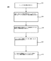
図1は、本発明の実施形態によって酸化ケイ素膜を作る方法100内の選択されたステップを示す流れ図である。方法100は、プラズマのない基板処理領域に炭素のないケイ素前駆体を提供するステップを含む(102)。炭素のないケイ素前駆体は、他の種のケイ素前駆体の中でも、たとえばケイ素および窒素前駆体、ケイ素および水素前駆体、またはケイ素、窒素、および水素含有前駆体とすることができる。ケイ素前駆体は、炭素がないことに加えて、酸素のないものにすることができる。酸素がない結果、これらの前駆体から形成されるケイ素および窒素層内のシラノール(Si−OH)基の濃度がより低くなる。堆積させた膜内の余分のシラノール部分は、堆積させた層からヒドロキシル(−OH)部分を除去する堆積後のステップ中に、多孔率および縮小率の増大を引き起こす可能性がある。
Exemplary Silicon Oxide Formation Process FIG. 1 is a flow diagram illustrating selected steps within a
炭素のないケイ素前駆体の特有の例は、他のシリル−アミンの中でも、H2N(SiH3)、HN(SiH3)2(すなわち、DSA)、およびN(SiH3)3(すなわち、TSA)などのシリル−アミンを含むことができる。異なる実施形態では、シリル−アミンの流量は、約200sccm以上、約300sccm以上、約500sccm以上、または約700sccm以上とすることができる。本明細書に与えるすべての流量は、デュアルチャンバ式の300mmの基板処理システムを指す。単一ウエハのシステムは、これらの流量の2分の1を必要とするはずであり、他のウエハ寸法は、処理される面積によって増減される流量を必要とするはずである。これらのシリル−アミンは、キャリアガス、反応ガス、または両方として作用できる追加のガスと混合することができる。これらの追加のガスの例は、他のガスの中でも、H2、N2、NH3、He、およびArを含むことができる。炭素のないケイ素前駆体の例はまた、シラン(SiH4)を単独で、または他のケイ素(たとえば、N(SiH3)3)、水素(たとえば、H2)、および/もしくは窒素(たとえば、N2、NH3)含有ガスと混合して含むことができる。炭素のないケイ素前駆体はまた、ジシラン、トリシラン、さらに高次のシラン、および塩化シランを単独で、または互いに組み合わせて、もしくは前述の炭素のないケイ素前駆体と組み合わせて含むことができる。
Specific examples of carbon-free silicon precursors are H 2 N (SiH 3 ), HN (SiH 3 ) 2 (ie, DSA), and N (SiH 3 ) 3 (ie, among other silyl-amines). Silyl-amines such as TSA) can be included. In different embodiments, the silyl-amine flow rate can be about 200 sccm or more, about 300 sccm or more, about 500 sccm or more, or about 700 sccm or more. All flow rates given herein refer to a
また、プラズマのない基板処理領域には、ラジカル窒素前駆体も提供される(104)。ラジカル窒素前駆体は、プラズマのない基板処理領域の外側で、より安定した窒素含有前駆体から生成された窒素ラジカル含有前駆体である。たとえば、NH3および/またはヒドラジン(N2H4)を含有する比較的安定した窒素含有前駆体を、チャンバプラズマ領域内、または処理チャンバの外側の遠隔プラズマシステム(RPS)内で活動化させて、ラジカル窒素前駆体を形成することができ、次いでラジカル窒素前駆体は、プラズマのない基板処理領域内へ輸送される。異なる実施形態では、安定した窒素前駆体はまた、NH3およびN2、NH3およびH2、NH3およびN2およびH2、ならびにN2およびH2を含む混合物とすることができる。N2およびH2を有する混合物中では、NH3の代わりに、またはNH3と組み合わせて、ヒドラジンを使用することもできる。異なる実施形態では、安定した窒素前駆体の流量は、約200sccm以上、約300sccm以上、約500sccm以上、または約700sccm以上とすることができる。チャンバプラズマ領域内で作られるラジカル窒素前駆体は、・N、・NH、・NH2などの1つまたは複数とすることができ、プラズマ内で形成されたイオン化種を伴うこともできる。 A radical nitrogen precursor is also provided (104) in the plasma-free substrate processing region. A radical nitrogen precursor is a nitrogen radical-containing precursor generated from a more stable nitrogen-containing precursor outside the plasma-free substrate processing region. For example, a relatively stable nitrogen-containing precursor containing NH 3 and / or hydrazine (N 2 H 4 ) can be activated in a chamber plasma region or in a remote plasma system (RPS) outside the processing chamber. A radical nitrogen precursor can be formed, which is then transported into a plasma-free substrate processing region. In different embodiments, the stable nitrogen precursor can also be a mixture comprising NH 3 and N 2 , NH 3 and H 2 , NH 3 and N 2 and H 2 , and N 2 and H 2 . The mixture with N 2 and H 2, in place of NH 3, or in combination with NH 3, can also be used hydrazine. In different embodiments, the stable nitrogen precursor flow rate can be about 200 sccm or more, about 300 sccm or more, about 500 sccm or more, or about 700 sccm or more. Radical nitrogen precursors produced in the chamber plasma region is, · N, · NH, can be one or more of such · NH 2, can also be accompanied by ionization species formed in the plasma.
チャンバプラズマ領域を用いる実施形態では、ラジカル窒素前駆体は、基板処理領域のうち、堆積領域から分割された一部分内で生成され、これらの前駆体が混合して反応し、堆積基板(たとえば、半導体ウエハ)上にケイ素および窒素層を堆積させる。 In embodiments using a chamber plasma region, radical nitrogen precursors are generated in a portion of the substrate processing region that is divided from the deposition region, and these precursors mix and react to form a deposition substrate (e.g., a semiconductor substrate). Silicon and nitrogen layers are deposited on the wafer.
プラズマのない基板処理領域には、ラジカル酸素前駆体が同時に提供される(106)。ラジカル酸素前駆体は、プラズマのない基板処理領域の外側で、より安定した酸素含有前駆体から生成された酸素ラジカル含有前駆体である。たとえば、O2、O3、H2O、H2O2、NO、NO2、および/またはN2Oを含有する安定した酸素含有前駆体化合物を、チャンバプラズマ領域内、または処理チャンバの外側の遠隔プラズマシステム(RPS)内で活動化させて、ラジカル酸素前駆体を形成することができ、次いでラジカル酸素前駆体は、プラズマのない基板処理領域内へ輸送される。ラジカル酸素前駆体は、ラジカル窒素前駆体と同じプラズマ内(チャンバプラズマ領域または共通のRPS内)で生成することができ、その場合、より安定した酸素含有前駆体とより安定した窒素含有前駆体をプラズマ領域内で組み合わせることができ、またはともに組み合わせてプラズマ領域内へ流すことができる。別法として、ラジカル酸素前駆体は、別個のプラズマ領域内で生成することができ、たとえば、ラジカル酸素前駆体はRPS内で生成することができ、ラジカル窒素前駆体はチャンバプラズマ領域内で生成することができる。異なる実施形態では、安定した酸素前駆体の流量は、約50sccm以上、約100sccm以上、約150sccm以上、約200sccm以上、または約250sccm以上とすることができる。異なる実施形態では、安定した酸素前駆体の流量は、約600sccm以下、約500sccm以下、約400sccm以下、または約300sccm以下とすることができる。開示する追加の実施形態によれば、これらの上限のいずれかを下限のいずれかと組み合わせて、安定した酸素前駆体の流量に対する追加の範囲を形成することができる。 A radical oxygen precursor is simultaneously provided (106) in a plasma-free substrate processing region. A radical oxygen precursor is an oxygen radical-containing precursor generated from a more stable oxygen-containing precursor outside the substrate processing region without plasma. For example, a stable oxygen-containing precursor compound containing O 2 , O 3 , H 2 O, H 2 O 2 , NO, NO 2 , and / or N 2 O can be placed in the chamber plasma region or outside the processing chamber. In a remote plasma system (RPS) to form a radical oxygen precursor, which is then transported into a plasma-free substrate processing region. The radical oxygen precursor can be generated in the same plasma (in the chamber plasma region or common RPS) as the radical nitrogen precursor, in which case a more stable oxygen-containing precursor and a more stable nitrogen-containing precursor are produced. They can be combined in the plasma region, or combined and flowed into the plasma region. Alternatively, the radical oxygen precursor can be generated in a separate plasma region, for example, the radical oxygen precursor can be generated in the RPS, and the radical nitrogen precursor is generated in the chamber plasma region. be able to. In different embodiments, the flow rate of the stable oxygen precursor may be about 50 seem or more, about 100 seem or more, about 150 seem or more, about 200 seem or more, or about 250 seem or more. In different embodiments, the flow rate of the stable oxygen precursor can be about 600 sccm or less, about 500 sccm or less, about 400 sccm or less, or about 300 sccm or less. According to additional embodiments disclosed, any of these upper limits can be combined with any of the lower limits to form additional ranges for stable oxygen precursor flow rates.
通常、窒素を含まないラジカル前駆体により、ケイ素および窒素含有層を形成することもできる。ラジカル前駆体は、前述の前駆体とともに遠隔プラズマ領域へ供給された窒素を含む場合、ラジカル窒素前駆体とすることができる。ラジカル前駆体は、反応チャンバのうち、堆積領域から分割された一部分内で生成され、これらの前駆体が混合して反応し、堆積基板(たとえば、半導体ウエハ)上にケイ素および窒素層を堆積させる。ラジカル前駆体がラジカル窒素前駆体である一実施形態では、安定した窒素前駆体が遠隔プラズマ領域内へ流れ、プラズマによって励起される。安定した窒素前駆体(およびラジカル窒素前駆体)はまた、水素(H2)、窒素(N2)、アルゴン、ヘリウムなどのキャリアガスを伴うことができる。開示する実施形態では、実質的に窒素(N2)からなる入力ガス(追加の不活性キャリアガスを有することもある)から形成されたラジカル窒素前駆体もまた、有益な膜を作り出すことがわかった。ケイ素含有前駆体が窒素を含む実施形態では、ラジカル窒素前駆体はまた、実質的に水素(H2)(および任意選択で、不活性キャリアガス)からなる入力ガスから形成されるラジカル前駆体と置き換えることもできる。 Usually, a silicon and nitrogen-containing layer can also be formed from a radical precursor that does not contain nitrogen. The radical precursor can be a radical nitrogen precursor when it includes nitrogen supplied to the remote plasma region along with the aforementioned precursor. Radical precursors are generated in a portion of the reaction chamber that is divided from the deposition region, and these precursors mix and react to deposit silicon and nitrogen layers on a deposition substrate (eg, a semiconductor wafer). . In one embodiment where the radical precursor is a radical nitrogen precursor, a stable nitrogen precursor flows into the remote plasma region and is excited by the plasma. Stable nitrogen precursors (and radical nitrogen precursors) can also be accompanied by a carrier gas such as hydrogen (H 2 ), nitrogen (N 2 ), argon, helium. In disclosed embodiments, it has been found that radical nitrogen precursors formed from an input gas consisting essentially of nitrogen (N 2 ) (which may have an additional inert carrier gas) also create a beneficial film. It was. In embodiments where the silicon-containing precursor comprises nitrogen, the radical nitrogen precursor also includes a radical precursor formed from an input gas consisting essentially of hydrogen (H 2 ) (and optionally an inert carrier gas) and It can also be replaced.
基板処理領域では、ラジカル窒素前駆体とラジカル酸素前駆体の並流が、炭素のないケイ素前駆体(プラズマによってあまり励起していない)と混合して反応し、堆積基板上にケイ素、酸素、および窒素含有膜を堆積させる(108)。低い流量(低い堆積速度)の場合、堆積させたケイ素および窒素含有膜は、共形に堆積させることができる。他の実施形態では、堆積させたケイ素および窒素含有膜は、従来の窒化ケイ素(Si3N4)膜堆積技法とは異なる流動特性を有する。形成物の流動性により、膜は、基板の堆積表面上の狭い間隙トレンチおよび他の構造内へ流れる。 In the substrate processing region, a cocurrent flow of radical nitrogen precursor and radical oxygen precursor mixes and reacts with a carbon-free silicon precursor (not much excited by the plasma), and on the deposition substrate silicon, oxygen, and A nitrogen-containing film is deposited (108). For low flow rates (low deposition rate), the deposited silicon and nitrogen containing films can be deposited conformally. In other embodiments, the deposited silicon and nitrogen containing films have different flow characteristics than conventional silicon nitride (Si 3 N 4 ) film deposition techniques. Due to the fluidity of the formation, the film flows into narrow gap trenches and other structures on the deposition surface of the substrate.
流動性は、ラジカル前駆体と炭素のないケイ素前駆体の混合に起因する様々な特性によって生じうる。これらの特性は、堆積させた膜内に相当な水素成分があること、および/または短鎖ポリシラザンポリマーが存在することを含むことができる。これらの短鎖は、成長して網をなし、膜の形成中および形成後に、より高密度の誘電体材料を形成する。たとえば、堆積させた膜は、シラザンタイプのSi−NH−Siバックボーン(すなわち、Si−N−H膜)を有することができる。ケイ素前駆体とラジカル前駆体のどちらにも炭素がないとき、堆積させたケイ素および窒素含有膜にもまた、実質上炭素がない。もちろん、「炭素がない」とは、膜に微量の炭素すらないことを必ずしも意味するわけではない。前駆体材料内には、堆積させたケイ素および窒素前駆体内へ入り込んだ炭素汚染物質が存在することがある。しかし、これらの炭素不純物の量は、炭素部分を有するケイ素前駆体(たとえば、TEOS、TMDSOなど)内で見られるはずの量よりはるかに少ない。本明細書に記載の実施形態で概説する流量の場合、堆積させたケイ素、酸素、および窒素含有膜の流動性は、あまり損なわれない。 Flowability can be caused by various properties resulting from the mixing of radical precursors and carbon-free silicon precursors. These properties can include the presence of significant hydrogen components in the deposited film and / or the presence of short chain polysilazane polymers. These short chains grow and network, forming a denser dielectric material during and after film formation. For example, the deposited film can have a silazane-type Si—NH—Si backbone (ie, a Si—N—H film). When neither the silicon precursor nor the radical precursor is free of carbon, the deposited silicon and nitrogen containing films are also substantially free of carbon. Of course, “no carbon” does not necessarily mean that the film does not contain trace amounts of carbon. Within the precursor material there may be carbon contaminants that have entered the deposited silicon and nitrogen precursors. However, the amount of these carbon impurities is much less than would be found in a silicon precursor having a carbon moiety (eg, TEOS, TMDSO, etc.). For the flow rates outlined in the embodiments described herein, the fluidity of the deposited silicon, oxygen, and nitrogen containing films is not significantly compromised.
ケイ素、酸素、および窒素含有層の堆積に続いて、酸素含有雰囲気中で堆積基板をアニールすることができる(110)。堆積基板は、酸素含有雰囲気が導入されるとき、硬化に使用されるのと同じ基板処理領域内に残すことができ、または異なるチャンバへ基板を移送することができ、そこで酸素含有雰囲気が導入される。酸素含有雰囲気は、他の酸素含有ガスの中でも、分子状酸素(O2)、オゾン(O3)、水蒸気(H2O)、過酸化水素(H2O2)、および酸化窒素(NO、NO2など)などの1つまたは複数の酸素含有ガスを含むことができる。酸素含有雰囲気はまた、遠隔で生成して基板チャンバ内へ輸送できる原子状酸素(O)、水酸化物(OH)などのラジカル酸素およびヒドロキシル種を含むことができる。酸素含有種のイオンが存在してもよい。異なる実施形態では、基板の酸素アニール温度は、約1100℃以下、約1000℃以下、約900℃以下、または約800℃以下とすることができる。異なる実施形態では、基板の温度は、約500℃以上、約600℃以上、約700℃以上、または約800℃以上とすることができる。この場合も、開示する追加の実施形態によれば、これらの上限のいずれかを下限のいずれかと組み合わせて、基板温度に対する追加の範囲を形成することができる。 Following deposition of the silicon, oxygen, and nitrogen containing layers, the deposition substrate can be annealed in an oxygen containing atmosphere (110). The deposition substrate can be left in the same substrate processing region used for curing when the oxygen-containing atmosphere is introduced, or the substrate can be transferred to a different chamber where the oxygen-containing atmosphere is introduced. The The oxygen-containing atmosphere is, among other oxygen-containing gases, molecular oxygen (O 2 ), ozone (O 3 ), water vapor (H 2 O), hydrogen peroxide (H 2 O 2 ), and nitrogen oxide (NO, One or more oxygen-containing gases such as NO 2 ). The oxygen-containing atmosphere can also include radical oxygen and hydroxyl species such as atomic oxygen (O), hydroxide (OH) that can be remotely generated and transported into the substrate chamber. Oxygen-containing species ions may be present. In different embodiments, the oxygen annealing temperature of the substrate can be about 1100 ° C. or less, about 1000 ° C. or less, about 900 ° C. or less, or about 800 ° C. or less. In different embodiments, the temperature of the substrate can be about 500 ° C. or higher, about 600 ° C. or higher, about 700 ° C. or higher, or about 800 ° C. or higher. Again, according to additional disclosed embodiments, any of these upper limits can be combined with any of the lower limits to form an additional range for the substrate temperature.
酸素アニール中、基板処理領域内には、プラズマが存在してもしなくてもよい。CVDチャンバに入る酸素含有ガスは、基板処理領域に入る前に活動化(たとえば、ラジカル化、イオン化など)させた1つまたは複数の化合物を含むことができる。たとえば、酸素含有ガスは、遠隔プラズマ源を通じて、またはシャワーヘッドによって基板処理領域から分離されたチャンバプラズマ領域を通じて、より安定した前駆体化合物を露出させることによって活動化させたラジカル酸素種、ラジカルヒドロキシル種などを含むことができる。より安定した前駆体は、ヒドロキシル(OH)ラジカルおよびイオンを作り出す水蒸気および過酸化水素(H2O2)、ならびに原子状酸素(O)ラジカルおよびイオンを作り出す分子状酸素および/またはオゾンを含むことができる。 During oxygen annealing, plasma may or may not be present in the substrate processing region. The oxygen-containing gas entering the CVD chamber can include one or more compounds that have been activated (eg, radicalized, ionized, etc.) prior to entering the substrate processing region. For example, the oxygen-containing gas can be activated by exposing a more stable precursor compound, radical hydroxyl species, through a remote plasma source or through a chamber plasma region separated from the substrate processing region by a showerhead. Etc. can be included. More stable precursors include water vapor and hydrogen peroxide (H 2 O 2 ) that create hydroxyl (OH) radicals and ions, and molecular oxygen and / or ozone that create atomic oxygen (O) radicals and ions Can do.
ケイ素、酸素、および窒素含有膜内に相当な酸素含有量が既に存在することを考えると、硬化動作は必要でないこともある。しかし、所望の場合、アニール動作の前に硬化動作が導入されるはずである。硬化中、堆積基板は、硬化用の基板処理領域内に残すことができ、または異なるチャンバへ基板を移送することができ、そこでオゾン含有雰囲気が導入される。異なる実施形態では、基板の硬化温度は、約400℃以下、約300℃以下、約250℃以下、約200℃以下、または約150℃以下とすることができる。異なる実施形態では、基板の温度は、ほぼ室温以上、約50℃以上、約100℃以上、約150℃以上、または約200℃以上とすることができる。開示する追加の実施形態によれば、これらの上限のいずれかを下限のいずれかと組み合わせて、基板温度に対する追加の範囲を形成することができる。実施形態では、表面付近の網を閉じて表面下の酸化を妨げることのある原子状酸素の生成を回避するために、基板処理領域内にはプラズマが存在しない。硬化ステップ中の基板処理領域内へのオゾンの流量は、約200sccm以上、約300sccm以上、または約500sccm以上とすることができる。硬化ステップ中のオゾンの分圧は、約10トル以上、約20トル以上、または約40トル以上とすることができる。いくつかの条件(たとえば、約100℃〜約200℃の基板温度)下では、変換が実質上完了したことがわかり、したがって実施形態では、酸素含有環境中での比較的高温のアニールは必要ないことがある。 Given that a substantial oxygen content already exists in the silicon, oxygen, and nitrogen containing films, a curing operation may not be necessary. However, if desired, a curing operation should be introduced before the annealing operation. During curing, the deposition substrate can be left in the substrate processing area for curing, or the substrate can be transferred to a different chamber where an ozone-containing atmosphere is introduced. In different embodiments, the curing temperature of the substrate can be about 400 ° C. or less, about 300 ° C. or less, about 250 ° C. or less, about 200 ° C. or less, or about 150 ° C. or less. In different embodiments, the temperature of the substrate can be about room temperature or higher, about 50 ° C. or higher, about 100 ° C. or higher, about 150 ° C. or higher, or about 200 ° C. or higher. According to additional disclosed embodiments, any of these upper limits can be combined with any of the lower limits to form an additional range for the substrate temperature. In an embodiment, no plasma is present in the substrate processing region to close the net near the surface and avoid the generation of atomic oxygen that can interfere with subsurface oxidation. The flow rate of ozone into the substrate processing region during the curing step can be about 200 sccm or more, about 300 sccm or more, or about 500 sccm or more. The partial pressure of ozone during the curing step can be about 10 Torr or more, about 20 Torr or more, or about 40 Torr or more. Under some conditions (eg, a substrate temperature of about 100 ° C. to about 200 ° C.), it can be seen that the conversion is substantially complete and, therefore, embodiments do not require a relatively high temperature anneal in an oxygen-containing environment. Sometimes.
硬化と酸素アニールの両方の酸素含有雰囲気は、酸素を提供してケイ素、酸素、および窒素含有膜を酸化ケイ素(SiO2)膜に変換する。前述のように、ケイ素、酸素、および窒素含有膜内に炭素がない結果、最終の酸化ケイ素膜内に形成される孔は著しく少なくなる。またその結果、酸化ケイ素への変換中の膜の体積の低減(すなわち、縮小率)がより小さくなる。たとえば、炭素含有ケイ素前駆体から形成されたケイ素−窒素−炭素層は、酸化ケイ素へ変換されるときに40体積%以上縮小することがあるが、実質上炭素のないケイ素および窒素膜は、約15体積%以下の縮小ですむことがある。 The oxygen-containing atmosphere of both curing and oxygen annealing provides oxygen to convert silicon, oxygen, and nitrogen containing films into silicon oxide (SiO 2 ) films. As mentioned above, the absence of carbon in the silicon, oxygen, and nitrogen containing film results in significantly fewer pores formed in the final silicon oxide film. As a result, the volume reduction (i.e., reduction ratio) of the film during conversion to silicon oxide is further reduced. For example, a silicon-nitrogen-carbon layer formed from a carbon-containing silicon precursor may shrink by more than 40% by volume when converted to silicon oxide, while silicon and nitrogen films substantially free of carbon are about It may be reduced by 15% by volume or less.
図2を次に参照すると、本発明の実施形態によって基板間隙(トレンチ)内に酸化ケイ素膜を形成する方法200内の選択されたステップを示す別の流れ図が示されている。方法200は、間隙を含む基板を基板処理領域内へ移送するステップを含むことができる(動作202)。基板は、基板上に形成されるデバイス構成要素(たとえば、トランジスタ)の間隔および構造のために、複数の間隙を有することができる。これらの間隙の高さおよび幅は、高さと幅(すなわち、H/W)のアスペクト比(AR)を画定することができ、このARは、1:1を著しく上回る(たとえば、5:1以上、6:1以上、7:1以上、8:1以上、9:1以上、10:1以上、11:1以上、12:1以上など)。多くの場合、高いARは、約90nm〜約22nm以下の範囲の小さい間隙幅(たとえば、約90nm、65nm、45nm、32nm、22nm、16nmなど)のために生じる。
Referring now to FIG. 2, another flow diagram illustrating selected steps within a
チャンバプラズマ領域内への安定した窒素前駆体および安定した酸素前駆体の並流は、ラジカル窒素前駆体およびラジカル酸素前駆体を形成する(動作204)。プラズマのない基板処理領域内で、プラズマによってあまり励起されていない炭素のないケイ素前駆体が、ラジカル窒素およびラジカル酸素前駆体と混合される(動作206)。基板上に、流動性の高いケイ素、酸素、および窒素含有層を堆積させることができる(動作208)。この層は流動性が高いため、高いアスペクト比を有する間隙を充填することができ、充填材料の中心の周りにボイドまたは弱いシームを生じさせない。たとえば、堆積する流動性の高い材料は、完全に充填する前に間隙の上部を早まって詰まらせて間隙の中間にボイドを残す可能性がより低い。 Cocurrent flow of a stable nitrogen precursor and a stable oxygen precursor into the chamber plasma region forms a radical nitrogen precursor and a radical oxygen precursor (operation 204). Within the plasma-free substrate processing region, carbon-free silicon precursors that are not significantly excited by the plasma are mixed with radical nitrogen and radical oxygen precursors (operation 206). A highly flowable silicon, oxygen, and nitrogen containing layer may be deposited on the substrate (operation 208). Because this layer is highly fluid, it can fill gaps with high aspect ratios and does not create voids or weak seams around the center of the filling material. For example, depositing highly fluid material is less likely to prematurely clog the top of the gap before it completely fills, leaving a void in the middle of the gap.
次いで、堆積させたケイ素、酸素、および窒素含有層を酸素含有雰囲気中でアニールし(動作210)、ケイ素、酸素、および窒素含有層を酸化ケイ素に遷移させることができる。酸化ケイ素層を高密度化するために、より高い基板温度の不活性環境中で、さらなるアニール(図示せず)を実施することもできる。この場合も、硬化ステップを実行して、酸化ケイ素への変換を助けることができ、このステップは、膜の形成(動作206)とアニール動作210の間に行われるはずである。
The deposited silicon, oxygen, and nitrogen containing layer can then be annealed in an oxygen containing atmosphere (operation 210) to transition the silicon, oxygen, and nitrogen containing layer to silicon oxide. In order to densify the silicon oxide layer, further annealing (not shown) can also be performed in an inert environment at a higher substrate temperature. Again, a curing step can be performed to assist in the conversion to silicon oxide, and this step should take place between film formation (operation 206) and
堆積させたケイ素、酸素、および窒素含有層を酸素含有雰囲気中でアニールすることで、基板間隙を含む酸化ケイ素層を基板上に形成する(210)。実施形態では、硬化およびアニールの処理パラメータは、図1を参照して説明したのと同じ範囲を保持する。上述したように、酸化ケイ素層では、熱処理ステップ前に著しい量の炭素が層内に存在する炭素含有前駆体で形成される類似の層より孔が少なく、体積の低減が小さい。多くの場合、体積の低減は、酸化ケイ素の縮小の結果として間隙内に形成される空間を充填、回復、または他の方法で除去する熱処理後のステップを回避できるほどわずかである(たとえば、約15体積%以下)。 The deposited silicon, oxygen, and nitrogen containing layer is annealed in an oxygen containing atmosphere to form a silicon oxide layer including the substrate gap on the substrate (210). In an embodiment, the curing and annealing process parameters remain in the same range as described with reference to FIG. As noted above, silicon oxide layers have fewer pores and less volume reduction than similar layers formed with carbon-containing precursors where a significant amount of carbon is present in the layer prior to the heat treatment step. In many cases, the volume reduction is so small that a post-heat treatment step that fills, recovers, or otherwise removes the space formed in the gap as a result of silicon oxide shrinkage can be avoided (e.g., about 15% by volume or less).
本発明をよりよく理解および評価するために、2つの膜をここで参照されたい。図2の処理の流れに従って第1の膜を成長させ、ラジカル酸素前駆体を持たないがそれ以外は類似の第2の膜を成長させた。これらの膜はそれぞれ、シャワーヘッドによってプラズマのない基板処理領域から分離されたチャンバプラズマ領域内へ、炭素のないケイ素および窒素含有前駆体としてTSAが275sccmの流量で供給され、アンモニア(NH3)が550sccmの流量で供給される状態で成長させた。分子状酸素(O2)は、アンモニアに使用されるものとは別個の入り口を通って同じくチャンバプラズマ領域内へ、150sccmの流量で供給した。分子状酸素は、第1の膜の成長中には供給したが、第2の膜の成長中には供給しなかった。第1の膜は、4800Å/分の堆積速度で成長し、第2の膜は、1650Å/分で成長した。堆積速度がより大きいことは、前述のように別個の硬化動作への依存が低減されることに加えて、さらなる利益である。第1の膜の屈折率(1.529)もまた、第2の膜の屈折率(1.5374)より小さく、堆積させた膜が酸化ケイ素の屈折率(1.46)により近いことを示す。 In order to better understand and evaluate the present invention, reference is now made to two membranes. A first film was grown in accordance with the process flow of FIG. 2, and a similar second film was grown without the radical oxygen precursor. Each of these films is supplied with TSA as a carbon-free silicon and nitrogen-containing precursor at a flow rate of 275 sccm into a chamber plasma region separated from a plasma-free substrate processing region by a showerhead, and ammonia (NH 3 ) is supplied. The growth was performed while supplying at a flow rate of 550 sccm. Molecular oxygen (O 2 ) was supplied at a flow rate of 150 sccm through the inlet separate from that used for ammonia and into the chamber plasma region. Molecular oxygen was supplied during the growth of the first film, but not during the growth of the second film. The first film was grown at a deposition rate of 4800 Å / min and the second film was grown at 1650 Å / min. The higher deposition rate is a further benefit in addition to the reduced dependence on separate curing operations as described above. The refractive index of the first film (1.529) is also smaller than the refractive index of the second film (1.5374), indicating that the deposited film is closer to the refractive index of silicon oxide (1.46). .
図3は、本発明の実施形態によって堆積中にO2が供給される場合および供給されない場合に得られるFTIRスペクトルのグラフである。流量は、TSAには275sccm、NH3には550sccm、および分子状酸素(使用時)には150sccmであった。分子状酸素およびアンモニアを使用してラジカル酸素およびラジカル窒素前駆体を作り、これらをプラズマのない基板処理領域内でTSAと組み合わせることで成長させて堆積させたケイ素、酸素、および窒素含有層に対するFTIRスペクトル302を示す。比較のため、堆積させたケイ素および窒素含有層に対するFTIRスペクトル304を示し、低温オゾン硬化後の同じ膜に対するスペクトル306も含む。FTIRピーク位置は、ラジカル酸素を用いて成長させた膜と、ラジカル酸素を用いないで成長させた膜で異なるが、ラジカル酸素を用いないで成長させた膜を硬化させた後、これらのピークはより類似する。実際には、ラジカル酸素前駆体を用いて成長させた膜の場合、膜内の酸素の存在に関連するこれらのピークはより大きい(302)。より高い酸素ピーク302は、硬化させた膜304と比較すると、膜内の酸素の存在がより多いことを示す。オゾンは、堆積させたケイ素および窒素含有膜を酸化させる際、膜の成長中のラジカル酸素露出ほど効果的でないことは明らかである。
FIG. 3 is a graph of FTIR spectra obtained with and without O 2 supply during deposition according to embodiments of the present invention. The flow rates were 275 sccm for TSA, 550 sccm for NH 3 , and 150 sccm for molecular oxygen (when used). FTIR for silicon, oxygen, and nitrogen containing layers grown using molecular oxygen and ammonia to create radical oxygen and radical nitrogen precursors and combined with TSA in a plasma-free substrate processing
例示的な酸化ケイ素堆積システム
本発明の実施形態を実施できる堆積チャンバは、他のタイプのチャンバの中でも、高密度プラズマ化学気相堆積(HDP−CVD)チャンバ、プラズマ化学気相堆積(PECVD)チャンバ、減圧化学気相堆積(SACVD)チャンバ、および熱化学気相堆積チャンバを含むことができる。本発明の実施形態を実施できるCVDシステムの特有の例には、カリフォルニア州サンタクララのApplied Materials,Inc.から入手可能なCENTURA ULTIMA(登録商標)HDP−CVDチャンバ/システム、およびPRODUCER(登録商標)PECVDチャンバ/システムが含まれる。
Exemplary Silicon Oxide Deposition System Deposition chambers in which embodiments of the present invention can be implemented are high density plasma chemical vapor deposition (HDP-CVD) chambers, plasma enhanced chemical vapor deposition (PECVD) chambers, among other types of chambers. , A low pressure chemical vapor deposition (SACVD) chamber, and a thermal chemical vapor deposition chamber. Specific examples of CVD systems in which embodiments of the present invention can be implemented include Applied Materials, Inc. of Santa Clara, California. CENTURA ULTIMA® HDP-CVD chamber / system and PRODUCER® PECVD chamber / system available from
本発明の例示的な方法とともに使用できる基板処理チャンバの例は、本願の譲受人に譲渡された「PROCESS CHAMBER FOR DIELECTRIC GAPFILL」という名称の2006年5月30日出願のLubomirskyらの米国仮特許出願第60/803,499号に図示および記載されているチャンバを含むことができる。同願の内容全体を、あらゆる目的で参照により本明細書に組み込む。追加の例示的なシステムは、米国特許第6,387,207号および第6,830,624号に図示および記載されているシステムを含むことができる。両特許もまた、あらゆる目的で参照により本明細書に組み込む。 An example of a substrate processing chamber that can be used with the exemplary method of the present invention is the United States provisional patent application of Lubomirsky et al. The chamber illustrated and described in 60 / 803,499 can be included. The entire contents of that application are incorporated herein by reference for all purposes. Additional exemplary systems can include the systems shown and described in US Pat. Nos. 6,387,207 and 6,830,624. Both patents are also incorporated herein by reference for all purposes.
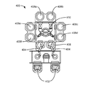
これらの堆積システムの実施形態は、集積回路チップを生産するより大型の製造システム内へ組み込むことができる。図4は、開示する実施形態による堆積チャンバ、焼成チャンバ、および硬化チャンバからなる1つのそのようなシステム400を示す。この図では、1対のFOUP(前方開口型統一ポッド)402が、基板(たとえば、直径300mmのウエハ)を供給し、基板はロボットアーム404によって受け取られ、低圧保持領域406内に配置されてから、ウエハ処理チャンバ408a〜fの1つに配置される。第2のロボットアーム410を使用して、基板ウエハを保持領域406から処理チャンバ408a〜fへ輸送し、また戻すことができる。
These deposition system embodiments can be incorporated into larger manufacturing systems that produce integrated circuit chips. FIG. 4 illustrates one
処理チャンバ408a〜fは、基板ウエハ上に流動性の高い誘電体膜を堆積、アニール、硬化、および/またはエッチングする1つまたは複数のシステム構成要素を含むことができる。一構成では、2対の処理チャンバ(たとえば、408c〜dおよび408e〜f)を使用して、基板上に流動性の高い誘電体材料を堆積させることができ、第3の対の処理チャンバ(たとえば、408a〜b)を使用して、堆積させた誘電体をアニールすることができる。別の構成では、同じ2対の処理チャンバ(たとえば、408c〜dおよび408e〜f)は、基板上で流動性の高い誘電体膜の堆積とアニールの両方を行うように構成することができ、第3の対のチャンバ(たとえば、408a〜b)は、堆積させた膜のUVまたは電子ビーム硬化に使用することができる。さらに別の構成では、3対のチャンバ(たとえば、408a〜f)をすべて、基板上で流動性の高い誘電体膜を堆積および硬化させるように構成することができる。さらに別の構成では、2対の処理チャンバ(たとえば、408c〜dおよび408e〜f)を使用して、流動性の高い誘電体の堆積とUVまたは電子ビーム硬化の両方を行うことができ、第3の対の処理チャンバ(たとえば、408a〜b)を使用して、誘電体膜をアニールすることができる。異なる実施形態では、図示の製造システムから分離されたチャンバ(複数可)上で、上記の処理のいずれか1つまたは複数を実施することができる。
The
さらに、処理チャンバ408a〜fの1つまたは複数を、湿式処理チャンバとして構成することができる。これらの処理チャンバは、湿気を含む雰囲気中で流動性の高い誘電体膜を加熱することを含む。したがって、システム400の実施形態は、堆積させた誘電体膜上で湿式アニールとドライアニールの両方を実行するために、湿式処理チャンバ408a〜bおよびアニール処理チャンバ408c〜dを含むことができる。
Further, one or more of the
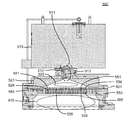
図5Aは、開示する実施形態による基板処理チャンバ500である。遠隔プラズマシステム(RPS)510は、ガスを処理することができ、このガスは次いで、ガス入り口アセンブリ511を通って進む。ガス入り口アセンブリ511内には、2つの個別のガス供給チャネルが見られる。第1のチャネル512は、遠隔プラズマシステムRPS510を通過するガスを運び、第2のチャネル513は、RPS510を迂回する。開示する実施形態では、第1のチャネル502は、プロセスガスに使用することができ、第2のチャネル513は、処理ガスに使用することができる。リッド(または導電性の上部部分)521および穿孔区画553が示されており、絶縁リング524が間に位置し、それによって穿孔区画553に対してリッド521に交流電位を印加することができる。プロセスガスは、第1のチャネル512を通ってチャンバプラズマ領域520内へ進み、チャンバプラズマ領域520内で単独で、またはRPS510と組み合わせて、プラズマによって励起することができる。本明細書では、チャンバプラズマ領域520および/またはRPS510の組合せを、遠隔プラズマシステムと呼ぶことができる。穿孔区画(シャワーヘッドとも呼ばれる)553は、シャワーヘッド553の下の基板処理領域570からチャンバプラズマ領域520を分離する。シャワーヘッド553により、チャンバプラズマ領域520内に存在するプラズマは、基板処理領域570内のガスを直接励起させるのを回避し、それでもなお励起種は、チャンバプラズマ領域520から基板処理領域570内へ進むことができる。
FIG. 5A is a
シャワーヘッド553は、チャンバプラズマ領域520と基板処理領域570の間に位置決めされ、チャンバプラズマ領域520内で生じたプラズマ廃水(前駆体または他のガスの励起された誘導体)は、板の厚さを横切る複数の貫通孔556を通過することができる。シャワーヘッド553はまた、1つまたは複数の中空の体積551を有し、中空の体積551は、蒸気またはガスの形の前駆体(ケイ素含有前駆体など)で充填することができ、直接チャンバプラズマ領域520内ではなく、小さい孔555を通って基板処理領域570内へ進むことができる。開示するこの実施形態では、シャワーヘッド553は、貫通孔556の最も小さい直径550の長さより厚い。チャンバプラズマ領域520から基板処理領域570へ浸透する相当な濃度の励起種を維持するために、貫通孔の最も小さい直径550の長さ526は、シャワーヘッド553の途中に貫通孔556の直径がより大きい部分を形成することによって制限することができる。開示する実施形態では、貫通孔556の最も小さい直径550の長さは、貫通孔556の最も小さい直径と同じ程度以下とすることができる。
The
図示の実施形態では、シャワーヘッド553は、チャンバプラズマ領域520内でプラズマによって励起されると、酸素、水素、および/もしくは窒素を含有するプロセスガス、ならびに/またはそのようなプロセスガスのプラズマ廃水を(貫通孔556を介して)分散させることができる。実施形態では、第1のチャネル512を通ってRPS510および/またはチャンバプラズマ領域520内へ導入されるプロセスガスは、酸素(O2)、オゾン(O3)、N2O、NO、NO2、NH3、N2H4を含むNxHy、シラン、ジシラン、TSA、およびDSAの1つまたは複数を含有することができる。プロセスガスはまた、ヘリウム、アルゴン、窒素(N2)などのキャリアガスを含むことができる。第2のチャネル513を通って、分子状酸素(または別の比較的安定した酸素含有ガス)を供給することができ、一方第1のチャネル512を通って、アンモニア(または別の比較的安定した窒素および水素含有ガス)を供給し、本明細書に前述したケイ素、酸素、および窒素含有膜を成長させる。別法として、酸素含有ガスと窒素および水素含有ガスを組み合わせることができ、どちらも、第1のチャネル512または第2のチャネル513を通って流れる。第2のチャネル513はまた、成長または堆積させた膜から望ましくない成分を除去するために使用されるキャリアガスおよび/または膜硬化ガスを供給することができる。プラズマ廃水は、プロセスガスのイオン化された誘導体または中性の誘導体を含むことができ、また本明細書では、導入されたプロセスガスの原子状の成分を指して、ラジカル酸素前駆体および/またはラジカル窒素前駆体と呼ぶこともできる。
In the illustrated embodiment, the
実施形態では、貫通孔556の数は、約60個〜約2000個とすることができる。貫通孔556は、様々な形状を有することができるが、円形に作るのが最も容易である。開示する実施形態では、貫通孔556の最も小さい直径550は、約0.5mm〜約20mmまたは約1mm〜約6mmとすることができる。貫通孔の断面形状の選択には許容範囲もあり、円錐形、円筒形、または2つの形状の組合せとすることができる。異なる実施形態では、基板処理領域570内へガスを導入するために使用される小さい孔555の数は、約100個〜約5000個または約500個〜約2000個とすることができる。小さい孔555の直径は、約0.1mm〜約2mmとすることができる。
In the embodiment, the number of through
図5Bは、開示する実施形態による処理チャンバとともに使用するためのシャワーヘッド553の底面図である。シャワーヘッド553は、図5Aに示すシャワーヘッドに相当する。貫通孔556が示されており、シャワーヘッド553の底部上で内径(ID)がより大きく、上部でIDがより小さい。小さい孔555は、貫通孔556の間でも、シャワーヘッドの表面全体にわたって実質上均一に分散され、それによって、本明細書に記載する他の実施形態より均一の混合を提供するのに役立つ。
FIG. 5B is a bottom view of a
シャワーヘッド553内の貫通孔556を通って到達するプラズマ廃水が、中空の体積551から小さい孔555を通って到達するケイ素含有前駆体と組み合わさるとき、基板処理領域570内でペデスタル(図示せず)によって支持された基板上に、例示的な膜が作られる。基板処理領域570は、硬化などの他の処理のためにプラズマに対応するように装備することができるが、例示的な膜の成長中にはプラズマは存在しない。
When the plasma wastewater that reaches through the through-
シャワーヘッド553の上のチャンバプラズマ領域520内で、またはシャワーヘッド553の下の基板処理領域570内で、プラズマを着火することができる。チャンバプラズマ領域520内にはプラズマが存在し、窒素および水素含有ガスならびに酸素含有ガスの流入から、ラジカル窒素およびラジカル酸素前駆体を作り出す。処理チャンバの導電性の上部部分521とシャワーヘッド553の間に、通常高周波(RF)範囲内の交流電圧を印加して、堆積中にチャンバプラズマ領域520内でプラズマを着火する。RF電源は、13.56MHzの高いRF周波数を生成するが、他の周波数を単独で、または13.56MHzの周波数と組み合わせて生成することもできる。
The plasma can be ignited in the
基板処理領域570内の底部プラズマを点けて膜を硬化させるとき、または基板処理領域570と境界をなす内部表面を洗浄するとき、上部プラズマは、低い出力、または出力のない状態のままとすることができる。基板処理領域570内のプラズマは、シャワーヘッド553とチャンバのペデスタルまたは底部の間に交流電圧を印加することによって着火される。プラズマが存在する間に、基板処理領域570内へ洗浄ガスを導入することができる。
When the film is cured by turning on the bottom plasma in the
ペデスタルは、熱交換チャネルを有することができ、このチャネルを通じて熱交換流体が流れ、基板の温度を制御する。この構成により、基板温度を冷却または加熱して、比較的低い温度(室温〜約120℃)を維持することができる。熱交換流体は、エチレングリコールおよび水を含むことができる。ペデスタルのウエハ支持プラター(好ましくは、アルミニウム、セラミック、またはこれらの組合せ)はまた、平行な同心円の形で完全に2回転するように構成された埋込み型の単一ループのヒータ要素を使用して、比較的高い温度(約120℃〜約1100℃)を実現するように抵抗加熱することができる。ヒータ要素の外側部分は、支持プラターの周囲に隣接することができ、内側部分は、より小さい半径を有する同心円の経路上に位置する。ヒータ要素への配線は、ペデスタルの軸を通過する。 The pedestal can have a heat exchange channel through which the heat exchange fluid flows and controls the temperature of the substrate. With this configuration, the substrate temperature can be cooled or heated to maintain a relatively low temperature (room temperature to about 120 ° C.). The heat exchange fluid can include ethylene glycol and water. Pedestal wafer support platters (preferably aluminum, ceramic, or combinations thereof) also use embedded single-loop heater elements configured to make two complete rotations in the form of parallel concentric circles. The resistance heating can be performed to achieve a relatively high temperature (about 120 ° C. to about 1100 ° C.). The outer portion of the heater element can be adjacent to the periphery of the support platter, and the inner portion is located on a concentric path having a smaller radius. The wiring to the heater element passes through the axis of the pedestal.
基板処理システムは、システムコントローラによって制御される。例示的な実施形態では、システムコントローラは、ハードディスクドライバ、フロッピーディスクドライバ、および処理装置を含む。処理装置は、単一基板コンピュータ(SBC)、アナログおよびデジタル入出力基板、インターフェース基板、ならびにステッパモータコントローラ基板を含む。CVDシステムの様々な部分は、基板、カードケージ、およびコネクタの寸法および型を規定するVersa Modular European(VME)標準に適合する。VME標準はまた、バス構造について、16ビットのデータバスおよび24ビットのアドレスバスを有すると規定する。 The substrate processing system is controlled by a system controller. In an exemplary embodiment, the system controller includes a hard disk driver, a floppy disk driver, and a processing device. The processing apparatus includes a single board computer (SBC), analog and digital input / output boards, interface boards, and stepper motor controller boards. The various parts of the CVD system meet the Versa Modular European (VME) standard that defines the dimensions and types of substrates, card cages, and connectors. The VME standard also defines the bus structure as having a 16-bit data bus and a 24-bit address bus.
システムコントローラは、CVD機械の活動のすべてを制御する。システムコントローラは、コンピュータ可読媒体内に記憶されたコンピュータプログラムであるシステム制御ソフトウェアを実行する。この媒体はハードディスクドライバであることが好ましいが、他の種類のメモリとすることもできる。コンピュータプログラムは、特定の処理のタイミング、ガスの混合、チャンバ圧力、チャンバ温度、RF出力レベル、サセプタの位置、および他のパラメータを指示する命令セットを含む。たとえばフロッピーディスクまたは別の適当なドライバを含む他のメモリデバイス上に記憶された他のコンピュータプログラムを使用して、システムコントローラに命令することもできる。 The system controller controls all of the activities of the CVD machine. The system controller executes system control software, which is a computer program stored in a computer readable medium. The medium is preferably a hard disk driver, but can be other types of memory. The computer program includes a set of instructions that indicate specific processing timing, gas mixing, chamber pressure, chamber temperature, RF power level, susceptor position, and other parameters. Other computer programs stored on other memory devices including, for example, a floppy disk or another suitable driver may be used to instruct the system controller.
基板上に積層膜を堆積させる処理またはチャンバを洗浄する処理は、システムコントローラによって実行されるコンピュータプログラム製品を使用して実施することができる。コンピュータプログラムコードは、任意の従来のコンピュータ可読プログラミング言語、たとえば68000アセンブリ言語、C、C++、Pascal、Fortranなどで書くことができる。適したプログラムコードは、従来のテキストエディタを使用して単一のファイルまたは複数のファイル内へ入力され、コンピュータのメモリシステムなどのコンピュータ使用可能媒体内で記憶または実施される。入力されたコードテキストが高級言語である場合、コードはコンパイルされ、その結果得られるコンパイラコードは次いで、事前にコンパイルされたMicrosoft Windows(登録商標)のライブラリルーチンのオブジェクトコードとリンクされる。リンクされたコンパイル済みのオブジェクトコードを実行するには、システムユーザは、オブジェクトコードを呼び出し、コンピュータシステムにコードをメモリ内へロードさせる。次いでCPUは、コードを読み取って実施し、プログラム内で識別されたタスクを実行する。 The process of depositing the laminated film on the substrate or the process of cleaning the chamber can be performed using a computer program product executed by the system controller. The computer program code can be written in any conventional computer readable programming language, such as 68000 assembly language, C, C ++, Pascal, Fortran, etc. Suitable program code is entered into a single file or multiple files using a conventional text editor and stored or implemented in a computer-usable medium, such as a computer memory system. If the entered code text is in a high-level language, the code is compiled and the resulting compiler code is then linked with the precompiled Microsoft Windows library object code. To execute the linked compiled object code, the system user calls the object code and causes the computer system to load the code into memory. The CPU then reads and executes the code to execute the task identified in the program.
ユーザとコントローラの間のインターフェースは、フラットパネル式の接触感知型モニタを介してなされる。好ましい実施形態では、2つのモニタが使用され、一方は、操作者用に洗浄室の壁に取り付けられ、他方は、サービス技術者用に壁の後ろに取り付けられる。2つのモニタは、同じ情報を同時に表示することができ、その場合、一度に一方のみが入力を受け入れる。特定のスクリーンまたは機能を選択するには、操作者は、接触感知型モニタの指定の領域に触れる。触れた領域では強調色が変化し、または新しいメニューもしくはスクリーンが表示され、操作者と接触感知型モニタの間の通信を確認する。接触感知型モニタの代わりに、またはそれに加えて、キーボード、マウス、または他のポインティングもしくは通信デバイスなどの他のデバイスを使用することができ、それによってユーザは、システムコントローラと通信することができる。 The interface between the user and the controller is made through a flat panel touch sensitive monitor. In a preferred embodiment, two monitors are used, one mounted on the wall of the washroom for the operator and the other mounted behind the wall for the service technician. Two monitors can display the same information simultaneously, in which case only one accepts input at a time. To select a particular screen or function, the operator touches a designated area of the touch sensitive monitor. The highlighted color changes in the touched area, or a new menu or screen is displayed, confirming communication between the operator and the touch-sensitive monitor. Instead of or in addition to a touch-sensitive monitor, other devices such as a keyboard, mouse, or other pointing or communication device can be used so that the user can communicate with the system controller.
チャンバプラズマ領域またはRPS内の領域は、遠隔プラズマ領域と呼ぶことができる。実施形態では、ラジカル前駆体(たとえば、ラジカル窒素前駆体)は、遠隔プラズマ領域内で作られ、基板処理領域内へ進み、基板処理領域内で、ラジカル前駆体によって炭素のないケイ素含有前駆体が励起される。実施形態では、炭素のないケイ素含有前駆体は、ラジカル前駆体によってのみ励起される。実施形態では、ラジカル前駆体が炭素のないケイ素含有前駆体への主な励起を提供するように、プラズマ出力は実質的に、遠隔プラズマ領域にのみ印加することができる。 The chamber plasma region or region within the RPS can be referred to as a remote plasma region. In embodiments, a radical precursor (eg, a radical nitrogen precursor) is created in the remote plasma region and proceeds into the substrate processing region, where the silicon-free precursor free of carbon is generated by the radical precursor. Excited. In embodiments, the carbon-free silicon-containing precursor is excited only by the radical precursor. In an embodiment, the plasma power can be applied substantially only to the remote plasma region so that the radical precursor provides the main excitation to the carbon-free silicon-containing precursor.
チャンバプラズマ領域を用いる実施形態では、基板処理領域のうち、堆積領域から分割された一部分内で、励起されたプラズマ廃水が生成される。本明細書では基板処理領域とも呼ばれる堆積領域は、プラズマ廃水が炭素のないケイ素含有前駆体と混合および反応してケイ素および窒素層を堆積基板(たとえば、半導体ウエハ)上に堆積させる領域である。励起されたプラズマ廃水はまた、不活性ガス(例示的な場合、アルゴン)を伴うことができる。実施形態では、炭素のないケイ素含有前駆体は、基板プラズマ領域に入る前にプラズマを通過しない。本明細書では、基板処理領域について、ケイ素および窒素含有層の成長中に「プラズマがない」と説明することができる。「プラズマがない」とは、この領域がプラズマを持たないことを必ずしも意味するわけではない。プラズマ領域内で作られるイオン化種および自由電子は、区画(シャワーヘッド)内の孔(開孔)を通って進むが、炭素のないケイ素含有前駆体は、プラズマ領域へ印加されるプラズマ出力によって実質上励起されない。チャンバプラズマ領域内のプラズマの境界は、画定するのが困難であるが、シャワーヘッド内の開孔を通って基板処理領域に侵入することがある。誘導結合されたプラズマの場合、基板処理領域内で直接、わずかな量のイオン化が生じることがある。さらに、形成される膜の所望の特徴をなくすことなく、基板処理領域内で低強度のプラズマが生じることがある。本明細書では、励起されたプラズマ廃水の生成中にチャンバプラズマ領域(またはその点では、遠隔プラズマ領域)よりはるかに低い強度のイオン密度を有するプラズマの原因はすべて、「プラズマがない」範囲から逸脱しない。 In embodiments using a chamber plasma region, excited plasma wastewater is generated in a portion of the substrate processing region that is divided from the deposition region. A deposition region, also referred to herein as a substrate processing region, is a region where plasma wastewater is mixed and reacted with a carbon-free silicon-containing precursor to deposit a silicon and nitrogen layer on a deposition substrate (eg, a semiconductor wafer). The excited plasma wastewater can also be accompanied by an inert gas (argon in the exemplary case). In embodiments, the carbon-free silicon-containing precursor does not pass through the plasma before entering the substrate plasma region. Herein, the substrate processing region can be described as “no plasma” during the growth of the silicon and nitrogen containing layer. “No plasma” does not necessarily mean that this region has no plasma. Ionized species and free electrons created in the plasma region travel through holes (openings) in the compartment (showerhead), whereas silicon-free precursors without carbon are substantially affected by the plasma power applied to the plasma region. Not excited. The plasma boundaries in the chamber plasma region are difficult to define, but can penetrate the substrate processing region through apertures in the showerhead. In the case of inductively coupled plasma, a small amount of ionization may occur directly in the substrate processing region. In addition, low intensity plasma may occur in the substrate processing region without losing the desired characteristics of the formed film. In this specification, all causes of a plasma having an ion density much lower than the chamber plasma region (or remote plasma region in that respect) during the generation of excited plasma wastewater are all from the “no plasma” range. Do not depart.
本明細書では、「基板」とは、層が上に形成されるかどうかにかかわらず、支持基板とすることができる。支持基板は、絶縁体、または様々なドーピング濃度およびプロファイルの半導体とすることができ、たとえば、集積回路の製造で使用されるタイプの半導体基板とすることができる。本明細書では、「酸化ケイ素」は、ケイ素および酸素含有材料の略称として区別なく使用される。したがって、酸化ケイ素は、窒素、水素、炭素などの他の元素成分の濃度を含むことができる。いくつかの実施形態では、本明細書に開示する方法を使用して作られる酸化ケイ素膜は実質的に、ケイ素および酸素からなる。「前駆体」という用語は、表面から材料を除去する反応、または表面上へ材料を堆積させる反応を担う任意のプロセスガスを指すために使用される。「励起状態」のガスとは、気体分子の少なくとも一部が振動励起、解離、および/またはイオン化された状態であるガスについて説明する。ガスは、2つ以上のガスの組合せとすることができる。「ラジカル前駆体」は、表面から材料を除去する反応、または表面上に材料を堆積させる反応を担うプラズマ廃水(プラズマを出る励起状態のガス)について説明するために使用される。「ラジカル水素前駆体」とは、水素を含有するラジカル前駆体であり、「ラジカル窒素前駆体」は、窒素を含有する。ラジカル窒素前駆体内には水素が存在することがあり、ラジカル水素前駆体内には窒素が存在することがある。「不活性ガス」という語句は、膜内へエッチングされ、または組み込まれたときに、化学結合を形成しない任意のガスを指す。例示的な不活性ガスには、希ガスが含まれるが、(通常)微量が膜内に取り込まれたときに化学結合が形成されない限り、他のガスを含むことができる。 As used herein, a “substrate” can be a support substrate regardless of whether a layer is formed thereon. The support substrate can be an insulator or a semiconductor of various doping concentrations and profiles, for example, a type of semiconductor substrate used in the manufacture of integrated circuits. In this specification, “silicon oxide” is used interchangeably as an abbreviation for silicon and oxygen-containing materials. Thus, silicon oxide can include concentrations of other elemental components such as nitrogen, hydrogen, and carbon. In some embodiments, the silicon oxide film made using the methods disclosed herein consists essentially of silicon and oxygen. The term “precursor” is used to refer to any process gas responsible for the reaction of removing material from a surface or depositing material on a surface. The term “excited state gas” refers to a gas in which at least a part of gas molecules are in a vibrationally excited, dissociated and / or ionized state. The gas can be a combination of two or more gases. “Radical precursor” is used to describe plasma wastewater (excited gas exiting the plasma) responsible for the reaction of removing material from the surface or depositing material on the surface. The “radical hydrogen precursor” is a radical precursor containing hydrogen, and the “radical nitrogen precursor” contains nitrogen. Hydrogen may be present in the radical nitrogen precursor, and nitrogen may be present in the radical hydrogen precursor. The phrase “inert gas” refers to any gas that does not form chemical bonds when etched or incorporated into a film. Exemplary inert gases include noble gases, but other gases can be included as long as no chemical bonds are formed when (usually) trace amounts are incorporated into the membrane.
本明細書全体にわたって「トレンチ」という用語を使用するが、エッチングされた幾何形状が大きい水平のアスペクト比を有することを示唆するものではない。表面の上から見ると、トレンチは、円形、楕円形、多角形、方形、または様々な他の形状に見えることがある。「ビア」という用語は、金属で充填して垂直の電気的接続を形成できるかどうかにかかわらず、アスペクト比が低いトレンチを指すために使用する。本明細書では、共形の層は、表面と同じ形状の表面上の概ね均一の材料層を指し、すなわち層の表面と覆われている表面は、概ね平行である。堆積させた材料を100%共形にすることはできない可能性が高く、したがって「概ね」という用語は許容公差を可能にすることが、当業者には理解されよう。 The term “trench” is used throughout this specification, but does not imply that the etched geometry has a large horizontal aspect ratio. When viewed from above the surface, the trenches may appear circular, elliptical, polygonal, square, or various other shapes. The term “via” is used to refer to a trench with a low aspect ratio, regardless of whether it can be filled with metal to form a vertical electrical connection. As used herein, a conformal layer refers to a generally uniform layer of material on a surface of the same shape as the surface, i.e., the surface of the layer and the surface being covered are generally parallel. One skilled in the art will appreciate that the deposited material is likely not to be 100% conformal and thus the term “generally” allows for acceptable tolerances.
いくつかの実施形態について説明したが、本発明の精神から逸脱することなく、様々な修正、代替構造、および均等物を使用できることが、当業者には理解されるであろう。さらに、本発明を不必要に曖昧にしないように、複数の周知の処理および要素については説明しなかった。したがって、上記の説明は、本発明の範囲を限定すると解釈されるべきではない。 While several embodiments have been described, those skilled in the art will appreciate that various modifications, alternative constructions, and equivalents can be used without departing from the spirit of the invention. Additionally, a number of well-known processes and elements have not been described in order not to unnecessarily obscure the present invention. Therefore, the above description should not be taken as limiting the scope of the invention.
値の範囲が提供される場合、その範囲の上限と下限の間に介在する各値もまた、文脈上別途明示しない限り、下限の単位の10分の1まで具体的に開示されることが理解される。任意の記載の値または記載の範囲内に介在する値と、任意の他の記載の値またはその記載の範囲内に介在する値との間のより小さい各範囲も包含される。これらのより小さい範囲の上限および下限は、別個に範囲内に包含または除外することができ、より小さい範囲内に限界のいずれかを含む範囲、どちらも含まない範囲、または両方を含む範囲もそれぞれ、記載の範囲内の任意の具体的に除外された限界に応じて、本発明の範囲内に包含される。記載の範囲が限界の一方または両方を含む場合、それらの含まれる限界の一方または両方を除外する範囲も含まれる。 Where a range of values is provided, it is understood that each value intervening between the upper and lower limits of the range is also specifically disclosed up to 1/10 of the lower limit unit unless the context clearly indicates otherwise. Is done. Also included are each smaller range between any stated value or value intervening in the stated range and any other stated value or value intervening in that stated range. The upper and lower limits of these smaller ranges may be separately included or excluded within the range, each including a range that includes any of the limits within the smaller range, a range that does not include both, or a range that includes both Are included within the scope of the invention, subject to any specifically excluded limits within the stated ranges. Where the stated range includes one or both of the limits, ranges excluding either or both of those included limits are also included.
本明細書および添付の特許請求の範囲では、単数形の名詞は、文脈上別途明示しない限り、複数の名詞を含む。したがって、たとえば、「処理」への言及は、複数のそのような処理を含み、「前駆体」への言及は、1つまたは複数の前駆体および当業者には知られているその均等物への言及を含み、以下同様である。 In this specification and the appended claims, a singular noun includes a plurality of nouns unless the context clearly indicates otherwise. Thus, for example, reference to “treatment” includes a plurality of such treatments, and reference to “precursor” refers to one or more precursors and equivalents thereof known to those skilled in the art. The same applies hereinafter.
また、「含む」、およびその文法的変形は、本明細書および以下の特許請求の範囲内で使用するとき、記載の特徴、整数、構成要素、またはステップの存在を指定するものであるが、1つまたは複数の他の特徴、整数、構成要素、ステップ、動作、または群の存在または追加を除外しない。 Also, "includes" and grammatical variations thereof, as used within the specification and the claims below, specify the presence of the described feature, integer, component, or step, It does not exclude the presence or addition of one or more other features, integers, components, steps, actions, or groups.
Claims (16)
第1のプラズマ領域内へ水素含有前駆体を流してラジカル前駆体を作り出しながら、第2のプラズマ領域内へ酸素含有前駆体を流してラジカル酸素前駆体を作り出すステップと、
前記プラズマのない基板処理領域内で、前記ラジカル前駆体および前記ラジカル酸素前駆体を炭素のないケイ素含有前駆体と同時に組み合わせるステップであって、前記水素含有前駆体および前記炭素のないケイ素含有前駆体の少なくとも1つが窒素を含有するステップと、
前記基板上にケイ素、酸素、および窒素含有層を堆積させるステップと、
酸素含有雰囲気においてアニール温度で前記ケイ素、酸素、および窒素含有層をアニールし、前記酸素含有量を増大させて前記窒素含有量を低減させることにより、酸化ケイ素層を形成するステップと
を含む方法。 A method of forming a silicon oxide layer on a substrate in a plasma-free substrate processing region within a substrate processing chamber comprising:
Flowing a hydrogen-containing precursor into the first plasma region to create a radical precursor while flowing an oxygen-containing precursor into the second plasma region to create a radical oxygen precursor;
Combining the radical precursor and the radical oxygen precursor simultaneously with a carbon-free silicon-containing precursor in the plasma-free substrate processing region, the hydrogen-containing precursor and the carbon-free silicon-containing precursor. At least one of containing nitrogen,
Depositing a silicon, oxygen, and nitrogen containing layer on the substrate;
Forming a silicon oxide layer by annealing the silicon, oxygen and nitrogen containing layer at an annealing temperature in an oxygen containing atmosphere and increasing the oxygen content to reduce the nitrogen content.
Applications Claiming Priority (5)
| Application Number | Priority Date | Filing Date | Title |
|---|---|---|---|
| US26586509P | 2009-12-02 | 2009-12-02 | |
| US61/265,865 | 2009-12-02 | ||
| US12/836,991 | 2010-07-15 | ||
| US12/836,991 US8980382B2 (en) | 2009-12-02 | 2010-07-15 | Oxygen-doping for non-carbon radical-component CVD films |
| PCT/US2010/056401 WO2011068652A2 (en) | 2009-12-02 | 2010-11-11 | Oxygen-doping for non-carbon radical-component cvd films |
Publications (2)
| Publication Number | Publication Date |
|---|---|
| JP2013513235A true JP2013513235A (en) | 2013-04-18 |
| JP2013513235A5 JP2013513235A5 (en) | 2013-12-26 |
Family
ID=44069100
Family Applications (1)
| Application Number | Title | Priority Date | Filing Date |
|---|---|---|---|
| JP2012542040A Pending JP2013513235A (en) | 2009-12-02 | 2010-11-11 | Oxygen doping for non-carbon radical component CVD films |
Country Status (7)
| Country | Link |
|---|---|
| US (1) | US8980382B2 (en) |
| JP (1) | JP2013513235A (en) |
| KR (1) | KR20120099270A (en) |
| CN (1) | CN102668045A (en) |
| SG (1) | SG181103A1 (en) |
| TW (1) | TWI507560B (en) |
| WO (1) | WO2011068652A2 (en) |
Cited By (6)
| Publication number | Priority date | Publication date | Assignee | Title |
|---|---|---|---|---|
| JP2015233137A (en) * | 2014-06-05 | 2015-12-24 | エーエスエム アイピー ホールディング ビー.ブイ. | Reactive curing process for semiconductor substrate |
| JP2017168644A (en) * | 2016-03-16 | 2017-09-21 | 大陽日酸株式会社 | Manufacturing method of semiconductor device and substrate processing method |
| JP2018524464A (en) * | 2015-03-30 | 2018-08-30 | レール・リキード−ソシエテ・アノニム・プール・レテュード・エ・レクスプロワタシオン・デ・プロセデ・ジョルジュ・クロード | Vapor deposition process for forming thin films containing silicon and oxygen |
| CN110612596A (en) * | 2017-04-13 | 2019-12-24 | 应用材料公司 | Method and apparatus for depositing low dielectric constant films |
| JP2020516079A (en) * | 2017-04-04 | 2020-05-28 | アプライド マテリアルズ インコーポレイテッドApplied Materials,Incorporated | Two-step process for silicon gap filling |
| JP2020517100A (en) * | 2017-04-07 | 2020-06-11 | アプライド マテリアルズ インコーポレイテッドApplied Materials,Incorporated | Gap filling using reactive annealing |
Families Citing this family (56)
| Publication number | Priority date | Publication date | Assignee | Title |
|---|---|---|---|---|
| US8232176B2 (en) | 2006-06-22 | 2012-07-31 | Applied Materials, Inc. | Dielectric deposition and etch back processes for bottom up gapfill |
| US7867923B2 (en) * | 2007-10-22 | 2011-01-11 | Applied Materials, Inc. | High quality silicon oxide films by remote plasma CVD from disilane precursors |
| US8357435B2 (en) | 2008-05-09 | 2013-01-22 | Applied Materials, Inc. | Flowable dielectric equipment and processes |
| US8741788B2 (en) | 2009-08-06 | 2014-06-03 | Applied Materials, Inc. | Formation of silicon oxide using non-carbon flowable CVD processes |
| US8449942B2 (en) | 2009-11-12 | 2013-05-28 | Applied Materials, Inc. | Methods of curing non-carbon flowable CVD films |
| CN102687252A (en) * | 2009-12-30 | 2012-09-19 | 应用材料公司 | Dielectric film growth with radicals produced using flexible nitrogen/hydrogen ratio |
| US8329262B2 (en) | 2010-01-05 | 2012-12-11 | Applied Materials, Inc. | Dielectric film formation using inert gas excitation |
| JP2013517616A (en) | 2010-01-06 | 2013-05-16 | アプライド マテリアルズ インコーポレイテッド | Flowable dielectrics using oxide liners |
| US8304351B2 (en) | 2010-01-07 | 2012-11-06 | Applied Materials, Inc. | In-situ ozone cure for radical-component CVD |
| WO2011109148A2 (en) | 2010-03-05 | 2011-09-09 | Applied Materials, Inc. | Conformal layers by radical-component cvd |
| US8236708B2 (en) * | 2010-03-09 | 2012-08-07 | Applied Materials, Inc. | Reduced pattern loading using bis(diethylamino)silane (C8H22N2Si) as silicon precursor |
| US8524004B2 (en) | 2010-06-16 | 2013-09-03 | Applied Materials, Inc. | Loadlock batch ozone cure |
| US8318584B2 (en) | 2010-07-30 | 2012-11-27 | Applied Materials, Inc. | Oxide-rich liner layer for flowable CVD gapfill |
| US9285168B2 (en) | 2010-10-05 | 2016-03-15 | Applied Materials, Inc. | Module for ozone cure and post-cure moisture treatment |
| US8664127B2 (en) | 2010-10-15 | 2014-03-04 | Applied Materials, Inc. | Two silicon-containing precursors for gapfill enhancing dielectric liner |
| US10283321B2 (en) | 2011-01-18 | 2019-05-07 | Applied Materials, Inc. | Semiconductor processing system and methods using capacitively coupled plasma |
| US8450191B2 (en) | 2011-01-24 | 2013-05-28 | Applied Materials, Inc. | Polysilicon films by HDP-CVD |
| KR101893471B1 (en) * | 2011-02-15 | 2018-08-30 | 어플라이드 머티어리얼스, 인코포레이티드 | Method and apparatus for multizone plasma generation |
| US8716154B2 (en) | 2011-03-04 | 2014-05-06 | Applied Materials, Inc. | Reduced pattern loading using silicon oxide multi-layers |
| US8445078B2 (en) | 2011-04-20 | 2013-05-21 | Applied Materials, Inc. | Low temperature silicon oxide conversion |
| US8466073B2 (en) * | 2011-06-03 | 2013-06-18 | Applied Materials, Inc. | Capping layer for reduced outgassing |
| US9404178B2 (en) | 2011-07-15 | 2016-08-02 | Applied Materials, Inc. | Surface treatment and deposition for reduced outgassing |
| US8617411B2 (en) * | 2011-07-20 | 2013-12-31 | Lam Research Corporation | Methods and apparatus for atomic layer etching |
| US8617989B2 (en) | 2011-09-26 | 2013-12-31 | Applied Materials, Inc. | Liner property improvement |
| US8551891B2 (en) | 2011-10-04 | 2013-10-08 | Applied Materials, Inc. | Remote plasma burn-in |
| DE102011084132A1 (en) | 2011-10-07 | 2013-04-11 | Schott Ag | glass role |
| WO2013054655A1 (en) * | 2011-10-14 | 2013-04-18 | 株式会社日立国際電気 | Method for manufacturing semiconductor device, substrate processing method, substrate processing apparatus, and recording medium |
| US10832904B2 (en) | 2012-06-12 | 2020-11-10 | Lam Research Corporation | Remote plasma based deposition of oxygen doped silicon carbide films |
| US10325773B2 (en) | 2012-06-12 | 2019-06-18 | Novellus Systems, Inc. | Conformal deposition of silicon carbide films |
| US9234276B2 (en) | 2013-05-31 | 2016-01-12 | Novellus Systems, Inc. | Method to obtain SiC class of films of desired composition and film properties |
| US8889566B2 (en) | 2012-09-11 | 2014-11-18 | Applied Materials, Inc. | Low cost flowable dielectric films |
| US20140099794A1 (en) * | 2012-09-21 | 2014-04-10 | Applied Materials, Inc. | Radical chemistry modulation and control using multiple flow pathways |
| US8822313B2 (en) * | 2012-12-20 | 2014-09-02 | Intermolecular, Inc. | Surface treatment methods and systems for substrate processing |
| US9018108B2 (en) | 2013-01-25 | 2015-04-28 | Applied Materials, Inc. | Low shrinkage dielectric films |
| US10297442B2 (en) | 2013-05-31 | 2019-05-21 | Lam Research Corporation | Remote plasma based deposition of graded or multi-layered silicon carbide film |
| KR102053350B1 (en) | 2013-06-13 | 2019-12-06 | 삼성전자주식회사 | Method of Semiconductor Device Having a low-k dielectric |
| US9343317B2 (en) | 2013-07-01 | 2016-05-17 | Micron Technology, Inc. | Methods of forming silicon-containing dielectric materials and semiconductor device structures |
| US9382269B2 (en) | 2013-09-27 | 2016-07-05 | Voltaix, Llc | Halogen free syntheses of aminosilanes by catalytic dehydrogenative coupling |
| US9371579B2 (en) * | 2013-10-24 | 2016-06-21 | Lam Research Corporation | Ground state hydrogen radical sources for chemical vapor deposition of silicon-carbon-containing films |
| US9412581B2 (en) | 2014-07-16 | 2016-08-09 | Applied Materials, Inc. | Low-K dielectric gapfill by flowable deposition |
| US9966240B2 (en) | 2014-10-14 | 2018-05-08 | Applied Materials, Inc. | Systems and methods for internal surface conditioning assessment in plasma processing equipment |
| US9355922B2 (en) | 2014-10-14 | 2016-05-31 | Applied Materials, Inc. | Systems and methods for internal surface conditioning in plasma processing equipment |
| US9777378B2 (en) * | 2015-01-07 | 2017-10-03 | Applied Materials, Inc. | Advanced process flow for high quality FCVD films |
| US11124876B2 (en) | 2015-03-30 | 2021-09-21 | L'Air Liquide, Société Anonyme pour l'Etude et l'Exploitation des Procédés Georges Claude | Si-containing film forming precursors and methods of using the same |
| US20160314964A1 (en) | 2015-04-21 | 2016-10-27 | Lam Research Corporation | Gap fill using carbon-based films |
| WO2017040623A1 (en) | 2015-09-01 | 2017-03-09 | Silcotek Corp. | Thermal chemical vapor deposition coating |
| US10087521B2 (en) | 2015-12-15 | 2018-10-02 | Silcotek Corp. | Silicon-nitride-containing thermal chemical vapor deposition coating |
| US10002787B2 (en) | 2016-11-23 | 2018-06-19 | Lam Research Corporation | Staircase encapsulation in 3D NAND fabrication |
| US10192734B2 (en) | 2016-12-11 | 2019-01-29 | L'Air Liquide, Société Anonyme pour l'Etude et l'Exploration des Procédés Georges Claude | Short inorganic trisilylamine-based polysilazanes for thin film deposition |
| US10840087B2 (en) | 2018-07-20 | 2020-11-17 | Lam Research Corporation | Remote plasma based deposition of boron nitride, boron carbide, and boron carbonitride films |
| CN113195786A (en) | 2018-10-19 | 2021-07-30 | 朗姆研究公司 | Remote hydrogen plasma exposure and doped or undoped silicon carbide deposition for gap fill |
| US11211243B2 (en) * | 2018-11-21 | 2021-12-28 | Taiwan Semiconductor Manufacturing Company, Ltd. | Method of filling gaps with carbon and nitrogen doped film |
| US11756786B2 (en) | 2019-01-18 | 2023-09-12 | International Business Machines Corporation | Forming high carbon content flowable dielectric film with low processing damage |
| WO2020252306A1 (en) | 2019-06-14 | 2020-12-17 | Silcotek Corp. | Nano-wire growth |
| CN111403396B (en) * | 2020-01-14 | 2021-11-23 | 长江存储科技有限责任公司 | Channel structure including tunneling layer with adjusted nitrogen weight percentage and method of forming the same |
| CN111599675A (en) * | 2020-05-25 | 2020-08-28 | 上海华力集成电路制造有限公司 | Self-aligned double patterning method |
Citations (10)
| Publication number | Priority date | Publication date | Assignee | Title |
|---|---|---|---|---|
| JP2001237243A (en) * | 1999-12-23 | 2001-08-31 | Asm America Inc | Manufacturing method and process of in-situ dielectric stack |
| US20060003596A1 (en) * | 2004-07-01 | 2006-01-05 | Micron Technology, Inc. | Low temperature process for polysilazane oxidation/densification |
| JP2006351689A (en) * | 2005-06-14 | 2006-12-28 | Tokyo Electron Ltd | Forming method of silicon oxide film, forming apparatus of silicon oxide film, and program |
| JP2007019145A (en) * | 2005-07-06 | 2007-01-25 | Tokyo Electron Ltd | Method of forming silicon oxynitride film, device of forming same and program |
| JP2008227511A (en) * | 2007-03-15 | 2008-09-25 | Applied Materials Inc | Improved gap-fill deposition in formation of silicon containing dielectric material |
| JP2008244490A (en) * | 1999-01-08 | 2008-10-09 | Toshiba Corp | Method of manufacturing semiconductor device |
| JP2008251959A (en) * | 2007-03-30 | 2008-10-16 | Tokyo Electron Ltd | Formation method of insulating layer, and manufacturing method of semiconductor device |
| JP2009170557A (en) * | 2008-01-12 | 2009-07-30 | Tokyo Electron Ltd | Film formation method and film formation apparatus |
| JP2009539269A (en) * | 2006-05-30 | 2009-11-12 | アプライド マテリアルズ インコーポレイテッド | Process chamber for dielectric gap filling |
| JP2009539268A (en) * | 2006-05-30 | 2009-11-12 | アプライド マテリアルズ インコーポレイテッド | Chemical vapor deposition of high quality fluidized silicon dioxide using silicon-containing precursors and atomic oxygen |
Family Cites Families (385)
| Publication number | Priority date | Publication date | Assignee | Title |
|---|---|---|---|---|
| US4147571A (en) * | 1977-07-11 | 1979-04-03 | Hewlett-Packard Company | Method for vapor epitaxial deposition of III/V materials utilizing organometallic compounds and a halogen or halide in a hot wall system |
| US4200666A (en) * | 1978-08-02 | 1980-04-29 | Texas Instruments Incorporated | Single component monomer for silicon nitride deposition |
| JPS61234534A (en) | 1985-04-11 | 1986-10-18 | Semiconductor Energy Lab Co Ltd | Fabrication of silicon nitride coating |
| FR2598520B1 (en) * | 1986-01-21 | 1994-01-28 | Seiko Epson Corp | MINERAL PROTECTIVE FILM |
| US4946593A (en) | 1987-03-31 | 1990-08-07 | Acushnet Company | Rubber composition for use with potable water |
| US4818326A (en) * | 1987-07-16 | 1989-04-04 | Texas Instruments Incorporated | Processing apparatus |
| US4910043A (en) * | 1987-07-16 | 1990-03-20 | Texas Instruments Incorporated | Processing apparatus and method |
| US4816098A (en) * | 1987-07-16 | 1989-03-28 | Texas Instruments Incorporated | Apparatus for transferring workpieces |
| JPH0616505B2 (en) | 1987-08-18 | 1994-03-02 | 株式会社半導体エネルギ−研究所 | Insulation film formation method |
| US4931354A (en) | 1987-11-02 | 1990-06-05 | Murata Manufacturing Co., Ltd. | Multilayer printed circuit board |
| JP2763100B2 (en) | 1988-02-03 | 1998-06-11 | 株式会社東芝 | Thin film formation method |
| JP2763104B2 (en) | 1988-03-16 | 1998-06-11 | 株式会社東芝 | Method of forming silicon oxide film |
| JPH01241826A (en) | 1988-03-23 | 1989-09-26 | Mitsubishi Electric Corp | Thin film forming device |
| JPH03197684A (en) | 1989-12-26 | 1991-08-29 | Anelva Corp | Adjacent plasma cvd device |
| JPH03257182A (en) | 1990-03-07 | 1991-11-15 | Hitachi Ltd | Surface processing device |
| JPH03286531A (en) | 1990-04-02 | 1991-12-17 | Kawasaki Steel Corp | Formation of silicon oxide film |
| US5016332A (en) | 1990-04-13 | 1991-05-21 | Branson International Plasma Corporation | Plasma reactor and process with wafer temperature control |
| US5620525A (en) * | 1990-07-16 | 1997-04-15 | Novellus Systems, Inc. | Apparatus for supporting a substrate and introducing gas flow doximate to an edge of the substrate |
| US5578532A (en) | 1990-07-16 | 1996-11-26 | Novellus Systems, Inc. | Wafer surface protection in a gas deposition process |
| US5843233A (en) | 1990-07-16 | 1998-12-01 | Novellus Systems, Inc. | Exclusion guard and gas-based substrate protection for chemical vapor deposition apparatus |
| KR930009549B1 (en) | 1990-11-28 | 1993-10-06 | 현대전자산업 주식회사 | High resistivity attaining method of poly-silicon |
| US5436172A (en) | 1991-05-20 | 1995-07-25 | Texas Instruments Incorporated | Real-time multi-zone semiconductor wafer temperature and process uniformity control system |
| US5426076A (en) | 1991-07-16 | 1995-06-20 | Intel Corporation | Dielectric deposition and cleaning process for improved gap filling and device planarization |
| JPH05259156A (en) | 1992-03-16 | 1993-10-08 | Fujitsu Ltd | Manufacture of semiconductor device |
| JPH05304147A (en) | 1992-04-27 | 1993-11-16 | Fujitsu Ltd | Fabrication of semiconductor device |
| US5279784A (en) * | 1992-05-05 | 1994-01-18 | Bandag Licensing Corporation | Method of fabrication of composite tire thread |
| JP3238744B2 (en) | 1992-05-15 | 2001-12-17 | 正俊 右高 | Method of manufacturing insulating film and method of manufacturing semiconductor device using this insulating film |
| US5356722A (en) | 1992-06-10 | 1994-10-18 | Applied Materials, Inc. | Method for depositing ozone/TEOS silicon oxide films of reduced surface sensitivity |
| US5271972A (en) | 1992-08-17 | 1993-12-21 | Applied Materials, Inc. | Method for depositing ozone/TEOS silicon oxide films of reduced surface sensitivity |
| US5393708A (en) * | 1992-10-08 | 1995-02-28 | Industrial Technology Research Institute | Inter-metal-dielectric planarization process |
| JP2684942B2 (en) * | 1992-11-30 | 1997-12-03 | 日本電気株式会社 | Chemical vapor deposition method, chemical vapor deposition apparatus, and method for manufacturing multilayer wiring |
| US5377139A (en) * | 1992-12-11 | 1994-12-27 | Motorola, Inc. | Process forming an integrated circuit |
| US5434109A (en) | 1993-04-27 | 1995-07-18 | International Business Machines Corporation | Oxidation of silicon nitride in semiconductor devices |
| US5587014A (en) | 1993-12-22 | 1996-12-24 | Sumitomo Chemical Company, Limited | Method for manufacturing group III-V compound semiconductor crystals |
| JP2645215B2 (en) | 1994-01-17 | 1997-08-25 | 株式会社東芝 | Thin film forming equipment |
| US5679152A (en) | 1994-01-27 | 1997-10-21 | Advanced Technology Materials, Inc. | Method of making a single crystals Ga*N article |
| US5547703A (en) | 1994-04-11 | 1996-08-20 | Dow Corning Corporation | Method of forming si-o containing coatings |
| JPH07316823A (en) | 1994-05-31 | 1995-12-05 | Sony Corp | Plasma cvd method and device therefor |
| US5468687A (en) | 1994-07-27 | 1995-11-21 | International Business Machines Corporation | Method of making TA2 O5 thin film by low temperature ozone plasma annealing (oxidation) |
| US5576071A (en) | 1994-11-08 | 1996-11-19 | Micron Technology, Inc. | Method of reducing carbon incorporation into films produced by chemical vapor deposition involving organic precursor compounds |
| JPH08148559A (en) | 1994-11-15 | 1996-06-07 | Fujitsu Ltd | Manufacture of semiconductor device with insulation film |
| US5530293A (en) | 1994-11-28 | 1996-06-25 | International Business Machines Corporation | Carbon-free hydrogen silsesquioxane with dielectric constant less than 3.2 annealed in hydrogen for integrated circuits |
| US5558717A (en) | 1994-11-30 | 1996-09-24 | Applied Materials | CVD Processing chamber |
| JPH08236518A (en) | 1995-02-28 | 1996-09-13 | Hitachi Ltd | Formation method of silicon oxide film |
| US5786263A (en) | 1995-04-04 | 1998-07-28 | Motorola, Inc. | Method for forming a trench isolation structure in an integrated circuit |
| JPH08288286A (en) | 1995-04-19 | 1996-11-01 | Sharp Corp | Silicon oxide film forming method |
| US5966595A (en) * | 1995-10-05 | 1999-10-12 | Micron Technology, Inc. | Method to form a DRAM capacitor using low temperature reoxidation |
| JPH09237785A (en) | 1995-12-28 | 1997-09-09 | Toshiba Corp | Semiconductor device and its manufacture |
| JP2871580B2 (en) | 1996-03-29 | 1999-03-17 | 日本電気株式会社 | Method for manufacturing semiconductor device |
| US6070551A (en) | 1996-05-13 | 2000-06-06 | Applied Materials, Inc. | Deposition chamber and method for depositing low dielectric constant films |
| US5827783A (en) | 1996-08-23 | 1998-10-27 | Mosel Vitelic, Inc. | Stacked capacitor having improved charge storage capacity |
| US5935340A (en) | 1996-11-13 | 1999-08-10 | Applied Materials, Inc. | Method and apparatus for gettering fluorine from chamber material surfaces |
| US5873781A (en) | 1996-11-14 | 1999-02-23 | Bally Gaming International, Inc. | Gaming machine having truly random results |
| JPH10163183A (en) | 1996-11-29 | 1998-06-19 | Sony Corp | Thin film forming equipment |
| US5811325A (en) | 1996-12-31 | 1998-09-22 | Industrial Technology Research Institute | Method of making a polysilicon carbon source/drain heterojunction thin-film transistor |
| FR2759362B1 (en) * | 1997-02-10 | 1999-03-12 | Saint Gobain Vitrage | TRANSPARENT SUBSTRATE EQUIPPED WITH AT LEAST ONE THIN LAYER BASED ON SILICON NITRIDE OR OXYNITRIDE AND ITS PROCESS FOR OBTAINING IT |
| US6090723A (en) | 1997-02-10 | 2000-07-18 | Micron Technology, Inc. | Conditioning of dielectric materials |
| TW388100B (en) | 1997-02-18 | 2000-04-21 | Hitachi Ulsi Eng Corp | Semiconductor deivce and process for producing the same |
| US5937308A (en) | 1997-03-26 | 1999-08-10 | Advanced Micro Devices, Inc. | Semiconductor trench isolation structure formed substantially within a single chamber |
| US6090442A (en) | 1997-04-14 | 2000-07-18 | University Technology Corporation | Method of growing films on substrates at room temperatures using catalyzed binary reaction sequence chemistry |
| US6551665B1 (en) | 1997-04-17 | 2003-04-22 | Micron Technology, Inc. | Method for improving thickness uniformity of deposited ozone-TEOS silicate glass layers |
| US5937323A (en) | 1997-06-03 | 1999-08-10 | Applied Materials, Inc. | Sequencing of the recipe steps for the optimal low-k HDP-CVD processing |
| US6207587B1 (en) * | 1997-06-24 | 2001-03-27 | Micron Technology, Inc. | Method for forming a dielectric |
| TW416100B (en) | 1997-07-02 | 2000-12-21 | Applied Materials Inc | Control of oxygen to silane ratio in a seasoning process to improve particle performance in an HDP-CVD system |
| US6114219A (en) | 1997-09-15 | 2000-09-05 | Advanced Micro Devices, Inc. | Method of manufacturing an isolation region in a semiconductor device using a flowable oxide-generating material |
| US6024044A (en) * | 1997-10-09 | 2000-02-15 | Applied Komatsu Technology, Inc. | Dual frequency excitation of plasma for film deposition |
| US6624064B1 (en) | 1997-10-10 | 2003-09-23 | Applied Materials, Inc. | Chamber seasoning method to improve adhesion of F-containing dielectric film to metal for VLSI application |
| US6566281B1 (en) | 1997-10-15 | 2003-05-20 | International Business Machines Corporation | Nitrogen-rich barrier layer and structures formed |
| US6087243A (en) | 1997-10-21 | 2000-07-11 | Advanced Micro Devices, Inc. | Method of forming trench isolation with high integrity, ultra thin gate oxide |
| US6017791A (en) | 1997-11-10 | 2000-01-25 | Taiwan Semiconductor Manufacturing Company | Multi-layer silicon nitride deposition method for forming low oxidation temperature thermally oxidized silicon nitride/silicon oxide (no) layer |
| JP3141827B2 (en) | 1997-11-20 | 2001-03-07 | 日本電気株式会社 | Method for manufacturing semiconductor device |
| US6009830A (en) * | 1997-11-21 | 2000-01-04 | Applied Materials Inc. | Independent gas feeds in a plasma reactor |
| KR100253079B1 (en) | 1997-12-01 | 2000-04-15 | 윤종용 | Semiconductor element trench isolation method |
| US6014791A (en) * | 1998-02-09 | 2000-01-18 | Soundesign, L.L.C. | Quiet vacuum cleaner using a vacuum pump with a lobed chamber |
| US6413583B1 (en) | 1998-02-11 | 2002-07-02 | Applied Materials, Inc. | Formation of a liquid-like silica layer by reaction of an organosilicon compound and a hydroxyl forming compound |
| US6054379A (en) | 1998-02-11 | 2000-04-25 | Applied Materials, Inc. | Method of depositing a low k dielectric with organo silane |
| JP3080061B2 (en) | 1998-03-19 | 2000-08-21 | 日本電気株式会社 | Method for forming element isolation region of semiconductor device |
| US6156394A (en) | 1998-04-17 | 2000-12-05 | Optical Coating Laboratory, Inc. | Polymeric optical substrate method of treatment |
| US6068884A (en) | 1998-04-28 | 2000-05-30 | Silcon Valley Group Thermal Systems, Llc | Method of making low κ dielectric inorganic/organic hybrid films |
| US6165834A (en) | 1998-05-07 | 2000-12-26 | Micron Technology, Inc. | Method of forming capacitors, method of processing dielectric layers, method of forming a DRAM cell |
| US6509283B1 (en) * | 1998-05-13 | 2003-01-21 | National Semiconductor Corporation | Thermal oxidation method utilizing atomic oxygen to reduce dangling bonds in silicon dioxide grown on silicon |
| US6146970A (en) | 1998-05-26 | 2000-11-14 | Motorola Inc. | Capped shallow trench isolation and method of formation |
| US6187682B1 (en) * | 1998-05-26 | 2001-02-13 | Motorola Inc. | Inert plasma gas surface cleaning process performed insitu with physical vapor deposition (PVD) of a layer of material |
| US6667553B2 (en) | 1998-05-29 | 2003-12-23 | Dow Corning Corporation | H:SiOC coated substrates |
| US6461970B1 (en) | 1998-06-10 | 2002-10-08 | Micron Technology, Inc. | Method of reducing defects in anti-reflective coatings and semiconductor structures fabricated thereby |
| US6302964B1 (en) | 1998-06-16 | 2001-10-16 | Applied Materials, Inc. | One-piece dual gas faceplate for a showerhead in a semiconductor wafer processing system |
| US6014979A (en) | 1998-06-22 | 2000-01-18 | Applied Materials, Inc. | Localizing cleaning plasma for semiconductor processing |
| US6406677B1 (en) | 1998-07-22 | 2002-06-18 | Eltron Research, Inc. | Methods for low and ambient temperature preparation of precursors of compounds of group III metals and group V elements |
| US6410149B1 (en) | 1998-08-27 | 2002-06-25 | Alliedsignal Inc. | Silane-based nanoporous silica thin films and precursors for making same |
| US6800571B2 (en) | 1998-09-29 | 2004-10-05 | Applied Materials Inc. | CVD plasma assisted low dielectric constant films |
| US6197658B1 (en) | 1998-10-30 | 2001-03-06 | Taiwan Semiconductor Manufacturing Company | Sub-atmospheric pressure thermal chemical vapor deposition (SACVD) trench isolation method with attenuated surface sensitivity |
| US6245690B1 (en) | 1998-11-04 | 2001-06-12 | Applied Materials, Inc. | Method of improving moisture resistance of low dielectric constant films |
| US6121130A (en) | 1998-11-16 | 2000-09-19 | Chartered Semiconductor Manufacturing Ltd. | Laser curing of spin-on dielectric thin films |
| US6583063B1 (en) | 1998-12-03 | 2003-06-24 | Applied Materials, Inc. | Plasma etching of silicon using fluorinated gas mixtures |
| TW445570B (en) * | 1998-12-11 | 2001-07-11 | United Microelectronics Corp | Manufacturing method for shallow trench isolation |
| US6469283B1 (en) | 1999-03-04 | 2002-10-22 | Applied Materials, Inc. | Method and apparatus for reducing thermal gradients within a substrate support |
| US6290774B1 (en) * | 1999-05-07 | 2001-09-18 | Cbl Technology, Inc. | Sequential hydride vapor phase epitaxy |
| US7091605B2 (en) | 2001-09-21 | 2006-08-15 | Eastman Kodak Company | Highly moisture-sensitive electronic device element and method for fabrication |
| US6180490B1 (en) * | 1999-05-25 | 2001-01-30 | Chartered Semiconductor Manufacturing Ltd. | Method of filling shallow trenches |
| US6204201B1 (en) * | 1999-06-11 | 2001-03-20 | Electron Vision Corporation | Method of processing films prior to chemical vapor deposition using electron beam processing |
| US6524931B1 (en) * | 1999-07-20 | 2003-02-25 | Motorola, Inc. | Method for forming a trench isolation structure in an integrated circuit |
| US6383954B1 (en) | 1999-07-27 | 2002-05-07 | Applied Materials, Inc. | Process gas distribution for forming stable fluorine-doped silicate glass and other films |
| US6602806B1 (en) | 1999-08-17 | 2003-08-05 | Applied Materials, Inc. | Thermal CVD process for depositing a low dielectric constant carbon-doped silicon oxide film |
| US6875687B1 (en) | 1999-10-18 | 2005-04-05 | Applied Materials, Inc. | Capping layer for extreme low dielectric constant films |
| DE60025872T2 (en) | 1999-10-25 | 2006-08-17 | Dow Corning Corp., Midland | Soluble silicone resin compositions |
| US6682659B1 (en) * | 1999-11-08 | 2004-01-27 | Taiwan Semiconductor Manufacturing Company | Method for forming corrosion inhibited conductor layer |
| JP2001144325A (en) * | 1999-11-12 | 2001-05-25 | Sony Corp | Method of manufacturing nitride iii-v compound semiconductor and semiconductor device |
| FI118804B (en) * | 1999-12-03 | 2008-03-31 | Asm Int | Process for making oxide films |
| US6150286A (en) | 2000-01-03 | 2000-11-21 | Advanced Micro Devices, Inc. | Method of making an ultra thin silicon nitride film |
| US6541367B1 (en) | 2000-01-18 | 2003-04-01 | Applied Materials, Inc. | Very low dielectric constant plasma-enhanced CVD films |
| US6440860B1 (en) * | 2000-01-18 | 2002-08-27 | Micron Technology, Inc. | Semiconductor processing methods of transferring patterns from patterned photoresists to materials, and structures comprising silicon nitride |
| US6461980B1 (en) | 2000-01-28 | 2002-10-08 | Applied Materials, Inc. | Apparatus and process for controlling the temperature of a substrate in a plasma reactor chamber |
| EP1124252A2 (en) * | 2000-02-10 | 2001-08-16 | Applied Materials, Inc. | Apparatus and process for processing substrates |
| EP1130633A1 (en) | 2000-02-29 | 2001-09-05 | STMicroelectronics S.r.l. | A method of depositing silicon oxynitride polimer layers |
| US7419903B2 (en) | 2000-03-07 | 2008-09-02 | Asm International N.V. | Thin films |
| US6558755B2 (en) | 2000-03-20 | 2003-05-06 | Dow Corning Corporation | Plasma curing process for porous silica thin film |
| WO2001074957A1 (en) | 2000-04-04 | 2001-10-11 | Asahi Kasei Kabushiki Kaisha | Coating composition for the production of insulating thin films |
| US6630413B2 (en) | 2000-04-28 | 2003-10-07 | Asm Japan K.K. | CVD syntheses of silicon nitride materials |
| US6387207B1 (en) | 2000-04-28 | 2002-05-14 | Applied Materials, Inc. | Integration of remote plasma generator with semiconductor processing chamber |
| US6495479B1 (en) * | 2000-05-05 | 2002-12-17 | Honeywell International, Inc. | Simplified method to produce nanoporous silicon-based films |
| US6553932B2 (en) | 2000-05-12 | 2003-04-29 | Applied Materials, Inc. | Reduction of plasma edge effect on plasma enhanced CVD processes |
| US6559026B1 (en) | 2000-05-25 | 2003-05-06 | Applied Materials, Inc | Trench fill with HDP-CVD process including coupled high power density plasma deposition |
| JP4371543B2 (en) | 2000-06-29 | 2009-11-25 | 日本電気株式会社 | Remote plasma CVD apparatus and film forming method |
| TW533489B (en) | 2000-06-30 | 2003-05-21 | Hitachi Ltd | Semiconductor device and production method thereof |
| US6835278B2 (en) | 2000-07-07 | 2004-12-28 | Mattson Technology Inc. | Systems and methods for remote plasma clean |
| US7183177B2 (en) * | 2000-08-11 | 2007-02-27 | Applied Materials, Inc. | Silicon-on-insulator wafer transfer method using surface activation plasma immersion ion implantation for wafer-to-wafer adhesion enhancement |
| US6614181B1 (en) | 2000-08-23 | 2003-09-02 | Applied Materials, Inc. | UV radiation source for densification of CVD carbon-doped silicon oxide films |
| US6566278B1 (en) | 2000-08-24 | 2003-05-20 | Applied Materials Inc. | Method for densification of CVD carbon-doped silicon oxide films through UV irradiation |
| CN1148228C (en) * | 2000-08-30 | 2004-05-05 | 夏家辉 | Gene medicine for treating hemophilia B and its preparing process |
| US6682969B1 (en) * | 2000-08-31 | 2004-01-27 | Micron Technology, Inc. | Top electrode in a strongly oxidizing environment |
| US6706634B1 (en) * | 2000-09-19 | 2004-03-16 | Infineon Technologies Ag | Control of separation between transfer gate and storage node in vertical DRAM |
| JP4232330B2 (en) * | 2000-09-22 | 2009-03-04 | 東京エレクトロン株式会社 | Excited gas forming apparatus, processing apparatus and processing method |
| JP3712356B2 (en) * | 2000-10-23 | 2005-11-02 | アプライド マテリアルズ インコーポレイテッド | Film-forming method and semiconductor device manufacturing method |
| US20020060322A1 (en) | 2000-11-20 | 2002-05-23 | Hiroshi Tanabe | Thin film transistor having high mobility and high on-current and method for manufacturing the same |
| US6287962B1 (en) | 2000-11-30 | 2001-09-11 | Taiwan Semiconductor Manufacturing Company | Method for making a novel graded silicon nitride/silicon oxide (SNO) hard mask for improved deep sub-micrometer semiconductor processing |
| US6531413B2 (en) | 2000-12-05 | 2003-03-11 | United Microelectronics Corp. | Method for depositing an undoped silicate glass layer |
| KR100385947B1 (en) | 2000-12-06 | 2003-06-02 | 삼성전자주식회사 | Method of forming thin film by atomic layer deposition |
| US6576564B2 (en) * | 2000-12-07 | 2003-06-10 | Micron Technology, Inc. | Photo-assisted remote plasma apparatus and method |
| US6930041B2 (en) | 2000-12-07 | 2005-08-16 | Micron Technology, Inc. | Photo-assisted method for semiconductor fabrication |
| US6538274B2 (en) | 2000-12-20 | 2003-03-25 | Micron Technology, Inc. | Reduction of damage in semiconductor container capacitors |
| US20020081817A1 (en) | 2000-12-22 | 2002-06-27 | Jayendra Bhakta | Void reduction and increased throughput in trench fill processes |
| US6660662B2 (en) * | 2001-01-26 | 2003-12-09 | Applied Materials, Inc. | Method of reducing plasma charge damage for plasma processes |
| US6599839B1 (en) | 2001-02-02 | 2003-07-29 | Advanced Micro Devices, Inc. | Plasma etch process for nonhomogenous film |
| US6589868B2 (en) | 2001-02-08 | 2003-07-08 | Applied Materials, Inc. | Si seasoning to reduce particles, extend clean frequency, block mobile ions and increase chamber throughput |
| KR100364026B1 (en) | 2001-02-22 | 2002-12-11 | 삼성전자 주식회사 | Method for forming inter layer dielectric film |
| US6632478B2 (en) | 2001-02-22 | 2003-10-14 | Applied Materials, Inc. | Process for forming a low dielectric constant carbon-containing film |
| US6447651B1 (en) | 2001-03-07 | 2002-09-10 | Applied Materials, Inc. | High-permeability magnetic shield for improved process uniformity in nonmagnetized plasma process chambers |
| KR100897771B1 (en) | 2001-03-13 | 2009-05-15 | 도쿄엘렉트론가부시키가이샤 | Film forming method and film forming apparatus |
| JP3990920B2 (en) | 2001-03-13 | 2007-10-17 | 東京エレクトロン株式会社 | Film forming method and film forming apparatus |
| CN1302152C (en) | 2001-03-19 | 2007-02-28 | 株式会社Ips | Chemical vapor depositing apparatus |
| EP1373595A1 (en) | 2001-03-23 | 2004-01-02 | Dow Corning Corporation | Method for producing hydrogenated silicon oxycarbide films |
| US6596576B2 (en) | 2001-04-10 | 2003-07-22 | Applied Materials, Inc. | Limiting hydrogen ion diffusion using multiple layers of SiO2 and Si3N4 |
| FR2824062B1 (en) * | 2001-04-27 | 2004-10-15 | Atofina | PROCESS FOR PRODUCING AQUEOUS SOLUTIONS OF QUATERNARY AMMONIUM UNSATURATED SALTS |
| US6528332B2 (en) * | 2001-04-27 | 2003-03-04 | Advanced Micro Devices, Inc. | Method and system for reducing polymer build up during plasma etch of an intermetal dielectric |
| US6780499B2 (en) | 2001-05-03 | 2004-08-24 | International Business Machines Corporation | Ordered two-phase dielectric film, and semiconductor device containing the same |
| US6596653B2 (en) | 2001-05-11 | 2003-07-22 | Applied Materials, Inc. | Hydrogen assisted undoped silicon oxide deposition process for HDP-CVD |
| US6716770B2 (en) | 2001-05-23 | 2004-04-06 | Air Products And Chemicals, Inc. | Low dielectric constant material and method of processing by CVD |
| US20020182893A1 (en) * | 2001-06-05 | 2002-12-05 | International Business Machines Corporation | Oxidation of silicon nitride films in semiconductor devices |
| JP2003017556A (en) * | 2001-06-29 | 2003-01-17 | Mitsubishi Electric Corp | Semiconductor device and method of manufacturing same |
| KR100421046B1 (en) * | 2001-07-13 | 2004-03-04 | 삼성전자주식회사 | Semiconductor device and method for manufacturing the same |
| US6548416B2 (en) * | 2001-07-24 | 2003-04-15 | Axcelis Technolgoies, Inc. | Plasma ashing process |
| SG187992A1 (en) | 2001-07-25 | 2013-03-28 | Univ Princeton | Nanochannel arrays and their preparation and use for high throughput macromolecular analysis |
| US6596654B1 (en) | 2001-08-24 | 2003-07-22 | Novellus Systems, Inc. | Gap fill for high aspect ratio structures |
| WO2003015129A2 (en) * | 2001-08-06 | 2003-02-20 | Advanced Technology Material, Inc. | Low-k dielectric thin films and chemical vapor deposition method of making same |
| US6531412B2 (en) | 2001-08-10 | 2003-03-11 | International Business Machines Corporation | Method for low temperature chemical vapor deposition of low-k films using selected cyclosiloxane and ozone gases for semiconductor applications |
| KR100428768B1 (en) * | 2001-08-29 | 2004-04-30 | 삼성전자주식회사 | Sti type semiconductor device and method of forming the same |
| US6756085B2 (en) | 2001-09-14 | 2004-06-29 | Axcelis Technologies, Inc. | Ultraviolet curing processes for advanced low-k materials |
| US6872323B1 (en) * | 2001-11-01 | 2005-03-29 | Novellus Systems, Inc. | In situ plasma process to remove fluorine residues from the interior surfaces of a CVD reactor |
| US6770521B2 (en) * | 2001-11-30 | 2004-08-03 | Texas Instruments Incorporated | Method of making multiple work function gates by implanting metals with metallic alloying additives |
| US6794290B1 (en) | 2001-12-03 | 2004-09-21 | Novellus Systems, Inc. | Method of chemical modification of structure topography |
| JP3891267B2 (en) | 2001-12-25 | 2007-03-14 | キヤノンアネルバ株式会社 | Silicon oxide film manufacturing method |
| US20030124873A1 (en) | 2001-12-28 | 2003-07-03 | Guangcai Xing | Method of annealing an oxide film |
| JP2003204063A (en) * | 2002-01-10 | 2003-07-18 | Toshiba Corp | Semiconductor device and its manufacturing method |
| US7175713B2 (en) | 2002-01-25 | 2007-02-13 | Applied Materials, Inc. | Apparatus for cyclical deposition of thin films |
| US6998014B2 (en) | 2002-01-26 | 2006-02-14 | Applied Materials, Inc. | Apparatus and method for plasma assisted deposition |
| US6911391B2 (en) | 2002-01-26 | 2005-06-28 | Applied Materials, Inc. | Integration of titanium and titanium nitride layers |
| DE10214065B4 (en) | 2002-03-28 | 2006-07-06 | Advanced Micro Devices, Inc., Sunnyvale | A method of making an improved metal silicide region in a silicon-containing conductive region in an integrated circuit |
| JP3868324B2 (en) | 2002-04-15 | 2007-01-17 | 三菱電機株式会社 | Silicon nitride film forming method, film forming apparatus, and semiconductor device manufacturing method |
| TW536775B (en) | 2002-04-18 | 2003-06-11 | Nanya Technology Corp | Manufacturing method of shallow trench isolation structure |
| WO2003090268A1 (en) | 2002-04-19 | 2003-10-30 | Tokyo Electron Limited | Method of treating substrate and process for producing semiconductor device |
| KR100468729B1 (en) | 2002-04-25 | 2005-01-29 | 삼성전자주식회사 | Method for Atomic Layer Deposition of silicon oxide film using HCD source |
| US6936551B2 (en) | 2002-05-08 | 2005-08-30 | Applied Materials Inc. | Methods and apparatus for E-beam treatment used to fabricate integrated circuit devices |
| US7307273B2 (en) * | 2002-06-07 | 2007-12-11 | Amberwave Systems Corporation | Control of strain in device layers by selective relaxation |
| TWI283899B (en) * | 2002-07-09 | 2007-07-11 | Applied Materials Inc | Capacitively coupled plasma reactor with magnetic plasma control |
| US7198866B2 (en) * | 2002-07-09 | 2007-04-03 | Nissan Motor Co., Ltd. | Cell assembly |
| US6900881B2 (en) | 2002-07-11 | 2005-05-31 | Molecular Imprints, Inc. | Step and repeat imprint lithography systems |
| US7294582B2 (en) | 2002-07-19 | 2007-11-13 | Asm International, N.V. | Low temperature silicon compound deposition |
| US6734082B2 (en) * | 2002-08-06 | 2004-05-11 | Chartered Semiconductor Manufacturing Ltd. | Method of forming a shallow trench isolation structure featuring a group of insulator liner layers located on the surfaces of a shallow trench shape |
| US6825097B2 (en) * | 2002-08-07 | 2004-11-30 | International Business Machines Corporation | Triple oxide fill for trench isolation |
| JP2004095889A (en) | 2002-08-30 | 2004-03-25 | Fasl Japan Ltd | Semiconductor storage device and its manufacturing method |
| KR100459724B1 (en) * | 2002-09-11 | 2004-12-03 | 삼성전자주식회사 | Semiconductor device having a SiN etch stopper by low temperature ALD and fabricating method the same |
| US7335609B2 (en) * | 2004-08-27 | 2008-02-26 | Applied Materials, Inc. | Gap-fill depositions introducing hydroxyl-containing precursors in the formation of silicon containing dielectric materials |
| US7456116B2 (en) | 2002-09-19 | 2008-11-25 | Applied Materials, Inc. | Gap-fill depositions in the formation of silicon containing dielectric materials |
| JP4358492B2 (en) * | 2002-09-25 | 2009-11-04 | レール・リキード−ソシエテ・アノニム・プール・レテュード・エ・レクスプロワタシオン・デ・プロセデ・ジョルジュ・クロード | Method for producing silicon nitride film or silicon oxynitride film by thermal chemical vapor deposition |
| US6828211B2 (en) | 2002-10-01 | 2004-12-07 | Taiwan Semiconductor Manufacturing Co., Ltd. | Shallow trench filled with two or more dielectrics for isolation and coupling or for stress control |
| US6833322B2 (en) | 2002-10-17 | 2004-12-21 | Applied Materials, Inc. | Apparatuses and methods for depositing an oxide film |
| US6819886B2 (en) | 2002-10-23 | 2004-11-16 | Nex Press Solutions Llc | Gloss/density measurement device with feedback to control gloss and density of images produced by an electrographic reproduction apparatus |
| US7080528B2 (en) | 2002-10-23 | 2006-07-25 | Applied Materials, Inc. | Method of forming a phosphorus doped optical core using a PECVD process |
| JP4142941B2 (en) | 2002-12-06 | 2008-09-03 | 株式会社東芝 | Manufacturing method of semiconductor device |
| US6858532B2 (en) | 2002-12-10 | 2005-02-22 | International Business Machines Corporation | Low defect pre-emitter and pre-base oxide etch for bipolar transistors and related tooling |
| US6900067B2 (en) | 2002-12-11 | 2005-05-31 | Lumileds Lighting U.S., Llc | Growth of III-nitride films on mismatched substrates without conventional low temperature nucleation layers |
| US7972663B2 (en) | 2002-12-20 | 2011-07-05 | Applied Materials, Inc. | Method and apparatus for forming a high quality low temperature silicon nitride layer |
| US6923189B2 (en) | 2003-01-16 | 2005-08-02 | Applied Materials, Inc. | Cleaning of CVD chambers using remote source with cxfyoz based chemistry |
| US6808748B2 (en) | 2003-01-23 | 2004-10-26 | Applied Materials, Inc. | Hydrogen assisted HDP-CVD deposition process for aggressive gap-fill technology |
| US7122222B2 (en) | 2003-01-23 | 2006-10-17 | Air Products And Chemicals, Inc. | Precursors for depositing silicon containing films and processes thereof |
| US7723242B2 (en) | 2004-03-15 | 2010-05-25 | Sharp Laboratories Of America, Inc. | Enhanced thin-film oxidation process |
| US7205248B2 (en) | 2003-02-04 | 2007-04-17 | Micron Technology, Inc. | Method of eliminating residual carbon from flowable oxide fill |
| US6884685B2 (en) | 2003-02-14 | 2005-04-26 | Freescale Semiconductors, Inc. | Radical oxidation and/or nitridation during metal oxide layer deposition process |
| US7084076B2 (en) | 2003-02-27 | 2006-08-01 | Samsung Electronics, Co., Ltd. | Method for forming silicon dioxide film using siloxane |
| US7098149B2 (en) | 2003-03-04 | 2006-08-29 | Air Products And Chemicals, Inc. | Mechanical enhancement of dense and porous organosilicate materials by UV exposure |
| US7429540B2 (en) | 2003-03-07 | 2008-09-30 | Applied Materials, Inc. | Silicon oxynitride gate dielectric formation using multiple annealing steps |
| US6867086B1 (en) * | 2003-03-13 | 2005-03-15 | Novellus Systems, Inc. | Multi-step deposition and etch back gap fill process |
| JP2004283065A (en) | 2003-03-20 | 2004-10-14 | Ushio Inc | Method for producing chemotaxic function control membrane, artificial material and method for producing artificial material |
| US7176144B1 (en) * | 2003-03-31 | 2007-02-13 | Novellus Systems, Inc. | Plasma detemplating and silanol capping of porous dielectric films |
| KR100505419B1 (en) | 2003-04-23 | 2005-08-04 | 주식회사 하이닉스반도체 | Method for manufacturing isolation layer in semiconductor device |
| JP4140768B2 (en) | 2003-04-24 | 2008-08-27 | 株式会社日立国際電気 | Semiconductor raw materials |
| JP3976703B2 (en) | 2003-04-30 | 2007-09-19 | エルピーダメモリ株式会社 | Manufacturing method of semiconductor device |
| US6830624B2 (en) | 2003-05-02 | 2004-12-14 | Applied Materials, Inc. | Blocker plate by-pass for remote plasma clean |
| US20040231590A1 (en) | 2003-05-19 | 2004-11-25 | Ovshinsky Stanford R. | Deposition apparatus for the formation of polycrystalline materials on mobile substrates |
| US6958112B2 (en) | 2003-05-27 | 2005-10-25 | Applied Materials, Inc. | Methods and systems for high-aspect-ratio gapfill using atomic-oxygen generation |
| JP2005033173A (en) | 2003-06-16 | 2005-02-03 | Renesas Technology Corp | Method for manufacturing semiconductor integrated circuit device |
| KR20050003758A (en) | 2003-07-04 | 2005-01-12 | 매그나칩 반도체 유한회사 | The method for forming shall trench isolation in semiconductor device |
| US7399388B2 (en) * | 2003-07-25 | 2008-07-15 | Applied Materials, Inc. | Sequential gas flow oxide deposition technique |
| US7192891B2 (en) * | 2003-08-01 | 2007-03-20 | Samsung Electronics, Co., Ltd. | Method for forming a silicon oxide layer using spin-on glass |
| US6818517B1 (en) | 2003-08-29 | 2004-11-16 | Asm International N.V. | Methods of depositing two or more layers on a substrate in situ |
| US7361991B2 (en) * | 2003-09-19 | 2008-04-22 | International Business Machines Corporation | Closed air gap interconnect structure |
| US20050121145A1 (en) | 2003-09-25 | 2005-06-09 | Du Bois Dale R. | Thermal processing system with cross flow injection system with rotatable injectors |
| JP4285184B2 (en) | 2003-10-14 | 2009-06-24 | 東京エレクトロン株式会社 | Film forming method and film forming apparatus |
| DE10350752A1 (en) | 2003-10-30 | 2005-06-09 | Infineon Technologies Ag | A method of forming a dielectric on a copper-containing metallization and capacitor assembly |
| US20050227017A1 (en) | 2003-10-31 | 2005-10-13 | Yoshihide Senzaki | Low temperature deposition of silicon nitride |
| JP4273932B2 (en) | 2003-11-07 | 2009-06-03 | 株式会社島津製作所 | Surface wave excitation plasma CVD equipment |
| AU2004313262B2 (en) | 2003-12-17 | 2009-06-04 | Cedraeus Inc. | Method for a random-based decision-making process |
| US7030468B2 (en) * | 2004-01-16 | 2006-04-18 | International Business Machines Corporation | Low k and ultra low k SiCOH dielectric films and methods to form the same |
| WO2005078784A1 (en) | 2004-02-17 | 2005-08-25 | Toagosei Co., Ltd. | Method for producing silicon oxide film |
| US7067438B2 (en) | 2004-02-19 | 2006-06-27 | Micron Technology, Inc. | Atomic layer deposition method of forming an oxide comprising layer on a substrate |
| US20050230350A1 (en) | 2004-02-26 | 2005-10-20 | Applied Materials, Inc. | In-situ dry clean chamber for front end of line fabrication |
| JP4279176B2 (en) | 2004-03-02 | 2009-06-17 | 株式会社アルバック | Method for forming silicon nitride film |
| US7087497B2 (en) | 2004-03-04 | 2006-08-08 | Applied Materials | Low-thermal-budget gapfill process |
| JP4451684B2 (en) | 2004-03-17 | 2010-04-14 | キヤノンアネルバ株式会社 | Vacuum processing equipment |
| KR20050094183A (en) | 2004-03-22 | 2005-09-27 | 삼성전자주식회사 | Chemical vapor deposition apparatus and method of forming an oxide layer using the same |
| US7524735B1 (en) | 2004-03-25 | 2009-04-28 | Novellus Systems, Inc | Flowable film dielectric gap fill process |
| US20050221020A1 (en) * | 2004-03-30 | 2005-10-06 | Tokyo Electron Limited | Method of improving the wafer to wafer uniformity and defectivity of a deposited dielectric film |
| US7115508B2 (en) | 2004-04-02 | 2006-10-03 | Applied-Materials, Inc. | Oxide-like seasoning for dielectric low k films |
| JP2005302848A (en) | 2004-04-07 | 2005-10-27 | Toshiba Corp | Semiconductor manufacturing equipment and semiconductor manufacturing method |
| US7125758B2 (en) | 2004-04-20 | 2006-10-24 | Applied Materials, Inc. | Controlling the properties and uniformity of a silicon nitride film by controlling the film forming precursors |
| US7109114B2 (en) | 2004-05-07 | 2006-09-19 | Applied Materials, Inc. | HDP-CVD seasoning process for high power HDP-CVD gapfil to improve particle performance |
| KR100580584B1 (en) | 2004-05-21 | 2006-05-16 | 삼성전자주식회사 | Method for cleaning a surface of a remote plasma generating tube and method and apparatus for processing a substrate using the same |
| US8119210B2 (en) | 2004-05-21 | 2012-02-21 | Applied Materials, Inc. | Formation of a silicon oxynitride layer on a high-k dielectric material |
| KR100762573B1 (en) * | 2004-06-04 | 2007-10-01 | 어플라이드 마이크로스트럭쳐스, 인코포레이티드 | Controlled vapor deposition of multilayered coating adhered by an oxide layer |
| US7297608B1 (en) | 2004-06-22 | 2007-11-20 | Novellus Systems, Inc. | Method for controlling properties of conformal silica nanolaminates formed by rapid vapor deposition |
| US7129187B2 (en) * | 2004-07-14 | 2006-10-31 | Tokyo Electron Limited | Low-temperature plasma-enhanced chemical vapor deposition of silicon-nitrogen-containing films |
| US7642171B2 (en) * | 2004-08-04 | 2010-01-05 | Applied Materials, Inc. | Multi-step anneal of thin films for film densification and improved gap-fill |
| US7294574B2 (en) * | 2004-08-09 | 2007-11-13 | Applied Materials, Inc. | Sputter deposition and etching of metallization seed layer for overhang and sidewall improvement |
| JP4470023B2 (en) | 2004-08-20 | 2010-06-02 | レール・リキード−ソシエテ・アノニム・プール・レテュード・エ・レクスプロワタシオン・デ・プロセデ・ジョルジュ・クロード | Method for manufacturing silicon nitride film |
| US7629270B2 (en) | 2004-08-27 | 2009-12-08 | Asm America, Inc. | Remote plasma activated nitridation |
| US20060046506A1 (en) * | 2004-09-01 | 2006-03-02 | Tokyo Electron Limited | Soft de-chucking sequence |
| KR100550351B1 (en) * | 2004-09-07 | 2006-02-08 | 삼성전자주식회사 | Method for forming a layer in a semiconductor device and apparatus for performing the same |
| TW200619416A (en) | 2004-09-30 | 2006-06-16 | Aviza Tech Inc | Method and apparatus for low temperature dielectric deposition using monomolecular precursors |
| US7148155B1 (en) | 2004-10-26 | 2006-12-12 | Novellus Systems, Inc. | Sequential deposition/anneal film densification method |
| US7226869B2 (en) | 2004-10-29 | 2007-06-05 | Lam Research Corporation | Methods for protecting silicon or silicon carbide electrode surfaces from morphological modification during plasma etch processing |
| KR100782369B1 (en) | 2004-11-11 | 2007-12-07 | 삼성전자주식회사 | Device for making semiconductor |
| US8193096B2 (en) * | 2004-12-13 | 2012-06-05 | Novellus Systems, Inc. | High dose implantation strip (HDIS) in H2 base chemistry |
| US20060154494A1 (en) | 2005-01-08 | 2006-07-13 | Applied Materials, Inc., A Delaware Corporation | High-throughput HDP-CVD processes for advanced gapfill applications |
| US20060162661A1 (en) | 2005-01-22 | 2006-07-27 | Applied Materials, Inc. | Mixing energized and non-energized gases for silicon nitride deposition |
| JP2006261434A (en) | 2005-03-17 | 2006-09-28 | L'air Liquide Sa Pour L'etude & L'exploitation Des Procede S Georges Claude | Method for forming silicon oxide film |
| US20060228903A1 (en) | 2005-03-30 | 2006-10-12 | Mcswiney Michael L | Precursors for the deposition of carbon-doped silicon nitride or silicon oxynitride films |
| US7972441B2 (en) | 2005-04-05 | 2011-07-05 | Applied Materials, Inc. | Thermal oxidation of silicon using ozone |
| KR100731164B1 (en) | 2005-05-19 | 2007-06-20 | 주식회사 피에조닉스 | Apparatus of chemical vapor deposition with a shower head and method therof |
| JP5091428B2 (en) * | 2005-06-14 | 2012-12-05 | 株式会社東芝 | Manufacturing method of semiconductor device |
| US20060286774A1 (en) | 2005-06-21 | 2006-12-21 | Applied Materials. Inc. | Method for forming silicon-containing materials during a photoexcitation deposition process |
| US7651955B2 (en) | 2005-06-21 | 2010-01-26 | Applied Materials, Inc. | Method for forming silicon-containing materials during a photoexcitation deposition process |
| US20070031598A1 (en) * | 2005-07-08 | 2007-02-08 | Yoshikazu Okuyama | Method for depositing silicon-containing films |
| JP4860953B2 (en) * | 2005-07-08 | 2012-01-25 | 富士通株式会社 | Silica-based film forming material, silica-based film and manufacturing method thereof, multilayer wiring and manufacturing method thereof, and semiconductor device and manufacturing method thereof |
| US20070010072A1 (en) * | 2005-07-09 | 2007-01-11 | Aviza Technology, Inc. | Uniform batch film deposition process and films so produced |
| US20070031609A1 (en) * | 2005-07-29 | 2007-02-08 | Ajay Kumar | Chemical vapor deposition chamber with dual frequency bias and method for manufacturing a photomask using the same |
| US7323401B2 (en) * | 2005-08-08 | 2008-01-29 | Applied Materials, Inc. | Semiconductor substrate process using a low temperature deposited carbon-containing hard mask |
| US7427570B2 (en) * | 2005-09-01 | 2008-09-23 | Micron Technology, Inc. | Porous organosilicate layers, and vapor deposition systems and methods for preparing same |
| US7544603B2 (en) * | 2005-09-22 | 2009-06-09 | United Microelectronics Corp. | Method of fabricating silicon nitride layer and method of fabricating semiconductor device |
| US7498270B2 (en) | 2005-09-30 | 2009-03-03 | Tokyo Electron Limited | Method of forming a silicon oxynitride film with tensile stress |
| US7901743B2 (en) | 2005-09-30 | 2011-03-08 | Tokyo Electron Limited | Plasma-assisted vapor phase treatment of low dielectric constant films using a batch processing system |
| JP5154009B2 (en) | 2005-10-21 | 2013-02-27 | 株式会社ジャパンディスプレイイースト | Manufacturing method of organic siloxane insulating film, and manufacturing method of liquid crystal display device using organic siloxane insulating film manufactured by this manufacturing method as interlayer insulation |
| US7884032B2 (en) | 2005-10-28 | 2011-02-08 | Applied Materials, Inc. | Thin film deposition |
| US20070099806A1 (en) | 2005-10-28 | 2007-05-03 | Stewart Michael P | Composition and method for selectively removing native oxide from silicon-containing surfaces |
| TWI332532B (en) | 2005-11-04 | 2010-11-01 | Applied Materials Inc | Apparatus and process for plasma-enhanced atomic layer deposition |
| US7521377B2 (en) | 2006-01-11 | 2009-04-21 | International Business Machines Corporation | SiCOH film preparation using precursors with built-in porogen functionality |
| JP5070702B2 (en) | 2006-01-19 | 2012-11-14 | 富士通セミコンダクター株式会社 | Semiconductor device manufacturing method and manufacturing apparatus |
| US7972954B2 (en) | 2006-01-24 | 2011-07-05 | Infineon Technologies Ag | Porous silicon dielectric |
| US7435661B2 (en) | 2006-01-27 | 2008-10-14 | Atmel Corporation | Polish stop and sealing layer for manufacture of semiconductor devices with deep trench isolation |
| JP4984558B2 (en) | 2006-02-08 | 2012-07-25 | 富士通セミコンダクター株式会社 | Manufacturing method of semiconductor device |
| JP4618178B2 (en) | 2006-03-27 | 2011-01-26 | オムロン株式会社 | Terminal and manufacturing method thereof |
| US7780865B2 (en) | 2006-03-31 | 2010-08-24 | Applied Materials, Inc. | Method to improve the step coverage and pattern loading for dielectric films |
| US7601651B2 (en) | 2006-03-31 | 2009-10-13 | Applied Materials, Inc. | Method to improve the step coverage and pattern loading for dielectric films |
| JP5149273B2 (en) | 2006-04-03 | 2013-02-20 | レール・リキード−ソシエテ・アノニム・プール・レテュード・エ・レクスプロワタシオン・デ・プロセデ・ジョルジュ・クロード | Method for depositing silicon nitride film and / or silicon oxynitride film by chemical vapor deposition |
| US7524750B2 (en) | 2006-04-17 | 2009-04-28 | Applied Materials, Inc. | Integrated process modulation (IPM) a novel solution for gapfill with HDP-CVD |
| US7902080B2 (en) * | 2006-05-30 | 2011-03-08 | Applied Materials, Inc. | Deposition-plasma cure cycle process to enhance film quality of silicon dioxide |
| US7498273B2 (en) * | 2006-05-30 | 2009-03-03 | Applied Materials, Inc. | Formation of high quality dielectric films of silicon dioxide for STI: usage of different siloxane-based precursors for harp II—remote plasma enhanced deposition processes |
| US7825038B2 (en) * | 2006-05-30 | 2010-11-02 | Applied Materials, Inc. | Chemical vapor deposition of high quality flow-like silicon dioxide using a silicon containing precursor and atomic oxygen |
| CN101326629B (en) * | 2006-05-30 | 2011-05-25 | 应用材料股份有限公司 | Process chamber for dielectric gapfill |
| US20070281106A1 (en) | 2006-05-30 | 2007-12-06 | Applied Materials, Inc. | Process chamber for dielectric gapfill |
| US7790634B2 (en) | 2006-05-30 | 2010-09-07 | Applied Materials, Inc | Method for depositing and curing low-k films for gapfill and conformal film applications |
| US20070289534A1 (en) * | 2006-05-30 | 2007-12-20 | Applied Materials, Inc. | Process chamber for dielectric gapfill |
| US8232176B2 (en) | 2006-06-22 | 2012-07-31 | Applied Materials, Inc. | Dielectric deposition and etch back processes for bottom up gapfill |
| US20080014759A1 (en) * | 2006-07-12 | 2008-01-17 | Applied Materials, Inc. | Method for fabricating a gate dielectric layer utilized in a gate structure |
| US20080038486A1 (en) * | 2006-08-03 | 2008-02-14 | Helmuth Treichel | Radical Assisted Batch Film Deposition |
| US8956457B2 (en) * | 2006-09-08 | 2015-02-17 | Tokyo Electron Limited | Thermal processing system for curing dielectric films |
| US7629273B2 (en) | 2006-09-19 | 2009-12-08 | Taiwan Semiconductor Manufacturing Company, Ltd. | Method for modulating stresses of a contact etch stop layer |
| TWI462179B (en) | 2006-09-28 | 2014-11-21 | Tokyo Electron Ltd | Film formation method and apparatus for forming silicon oxide film |
| US7737050B2 (en) | 2006-10-30 | 2010-06-15 | International Business Machines Corporation | Method of fabricating a nitrided silicon oxide gate dielectric layer |
| US7943005B2 (en) | 2006-10-30 | 2011-05-17 | Applied Materials, Inc. | Method and apparatus for photomask plasma etching |
| US20080102223A1 (en) | 2006-11-01 | 2008-05-01 | Sigurd Wagner | Hybrid layers for use in coatings on electronic devices or other articles |
| US7749574B2 (en) | 2006-11-14 | 2010-07-06 | Applied Materials, Inc. | Low temperature ALD SiO2 |
| US7939422B2 (en) | 2006-12-07 | 2011-05-10 | Applied Materials, Inc. | Methods of thin film process |
| JP5177617B2 (en) | 2006-12-25 | 2013-04-03 | 独立行政法人産業技術総合研究所 | Silicon oxide thin film forming equipment |
| US8017522B2 (en) | 2007-01-24 | 2011-09-13 | International Business Machines Corporation | Mechanically robust metal/low-κ interconnects |
| US7572647B2 (en) | 2007-02-02 | 2009-08-11 | Applied Materials, Inc. | Internal balanced coil for inductively coupled high density plasma processing chamber |
| KR100800495B1 (en) | 2007-02-27 | 2008-02-04 | 삼성전자주식회사 | Method of fabricating semiconductor device |
| JP2008218684A (en) | 2007-03-05 | 2008-09-18 | Sony Corp | Method of fabricating semiconductor device |
| US7964441B2 (en) | 2007-03-30 | 2011-06-21 | Tokyo Electron Limited | Catalyst-assisted atomic layer deposition of silicon-containing films with integrated in-situ reactive treatment |
| US7781352B2 (en) | 2007-06-06 | 2010-08-24 | Asm Japan K.K. | Method for forming inorganic silazane-based dielectric film |
| JP2009027134A (en) | 2007-06-21 | 2009-02-05 | Tokyo Electron Ltd | Mos semiconductor memory device |
| KR100866143B1 (en) * | 2007-08-03 | 2008-10-31 | 주식회사 하이닉스반도체 | Method for forming isolation layer of semiconductor device |
| US7745352B2 (en) * | 2007-08-27 | 2010-06-29 | Applied Materials, Inc. | Curing methods for silicon dioxide thin films deposited from alkoxysilane precursor with harp II process |
| EP2193541A1 (en) * | 2007-09-18 | 2010-06-09 | L'AIR LIQUIDE, Société Anonyme pour l'Etude et l'Exploitation des Procédés Georges Claude | Method of forming silicon-containing films |
| US20090095714A1 (en) | 2007-10-12 | 2009-04-16 | Tokyo Electron Limited | Method and system for low pressure plasma processing |
| US7867923B2 (en) * | 2007-10-22 | 2011-01-11 | Applied Materials, Inc. | High quality silicon oxide films by remote plasma CVD from disilane precursors |
| US7943531B2 (en) | 2007-10-22 | 2011-05-17 | Applied Materials, Inc. | Methods for forming a silicon oxide layer over a substrate |
| US7803722B2 (en) * | 2007-10-22 | 2010-09-28 | Applied Materials, Inc | Methods for forming a dielectric layer within trenches |
| US7541297B2 (en) | 2007-10-22 | 2009-06-02 | Applied Materials, Inc. | Method and system for improving dielectric film quality for void free gap fill |
| US7651959B2 (en) | 2007-12-03 | 2010-01-26 | Asm Japan K.K. | Method for forming silazane-based dielectric film |
| US8501637B2 (en) | 2007-12-21 | 2013-08-06 | Asm International N.V. | Silicon dioxide thin films by ALD |
| US7659184B2 (en) | 2008-02-25 | 2010-02-09 | Applied Materials, Inc. | Plasma immersion ion implantation process with chamber seasoning and seasoning layer plasma discharging for wafer dechucking |
| US7737052B2 (en) | 2008-03-05 | 2010-06-15 | International Business Machines Corporation | Advanced multilayer dielectric cap with improved mechanical and electrical properties |
| US7659158B2 (en) | 2008-03-31 | 2010-02-09 | Applied Materials, Inc. | Atomic layer deposition processes for non-volatile memory devices |
| JP2009267366A (en) | 2008-04-02 | 2009-11-12 | Nec Electronics Corp | Semiconductor memory and method of manufacturing the same |
| US8357435B2 (en) | 2008-05-09 | 2013-01-22 | Applied Materials, Inc. | Flowable dielectric equipment and processes |
| US20090277587A1 (en) | 2008-05-09 | 2009-11-12 | Applied Materials, Inc. | Flowable dielectric equipment and processes |
| US20090289284A1 (en) | 2008-05-23 | 2009-11-26 | Chartered Semiconductor Manufacturing, Ltd. | High shrinkage stress silicon nitride (SiN) layer for NFET improvement |
| KR20090122860A (en) | 2008-05-26 | 2009-12-01 | 주성엔지니어링(주) | Polysilicon film and method of forming the same, flash memory device and manufacturing method using the same |
| US7622369B1 (en) | 2008-05-30 | 2009-11-24 | Asm Japan K.K. | Device isolation technology on semiconductor substrate |
| US20090325391A1 (en) | 2008-06-30 | 2009-12-31 | Asm International Nv | Ozone and teos process for silicon oxide deposition |
| US8129555B2 (en) * | 2008-08-12 | 2012-03-06 | Air Products And Chemicals, Inc. | Precursors for depositing silicon-containing films and methods for making and using same |
| JP4638550B2 (en) | 2008-09-29 | 2011-02-23 | 東京エレクトロン株式会社 | Mask pattern forming method, fine pattern forming method, and film forming apparatus |
| US20100081293A1 (en) | 2008-10-01 | 2010-04-01 | Applied Materials, Inc. | Methods for forming silicon nitride based film or silicon carbon based film |
| US20100136313A1 (en) | 2008-12-01 | 2010-06-03 | Asm Japan K.K. | Process for forming high resistivity thin metallic film |
| US8765233B2 (en) | 2008-12-09 | 2014-07-01 | Asm Japan K.K. | Method for forming low-carbon CVD film for filling trenches |
| JP2010183069A (en) | 2009-01-07 | 2010-08-19 | Hitachi Kokusai Electric Inc | Manufacturing method of semiconductor device and substrate processing apparatus |
| US7919416B2 (en) | 2009-01-21 | 2011-04-05 | Asm Japan K.K. | Method of forming conformal dielectric film having Si-N bonds by PECVD |
| US7972980B2 (en) | 2009-01-21 | 2011-07-05 | Asm Japan K.K. | Method of forming conformal dielectric film having Si-N bonds by PECVD |
| US7935643B2 (en) * | 2009-08-06 | 2011-05-03 | Applied Materials, Inc. | Stress management for tensile films |
| US8741788B2 (en) * | 2009-08-06 | 2014-06-03 | Applied Materials, Inc. | Formation of silicon oxide using non-carbon flowable CVD processes |
| US7989365B2 (en) * | 2009-08-18 | 2011-08-02 | Applied Materials, Inc. | Remote plasma source seasoning |
| US8329587B2 (en) * | 2009-10-05 | 2012-12-11 | Applied Materials, Inc. | Post-planarization densification |
| US8466067B2 (en) * | 2009-10-05 | 2013-06-18 | Applied Materials, Inc. | Post-planarization densification |
| US20110136347A1 (en) | 2009-10-21 | 2011-06-09 | Applied Materials, Inc. | Point-of-use silylamine generation |
| US8449942B2 (en) * | 2009-11-12 | 2013-05-28 | Applied Materials, Inc. | Methods of curing non-carbon flowable CVD films |
| US20110159213A1 (en) | 2009-12-30 | 2011-06-30 | Applied Materials, Inc. | Chemical vapor deposition improvements through radical-component modification |
| CN102687252A (en) * | 2009-12-30 | 2012-09-19 | 应用材料公司 | Dielectric film growth with radicals produced using flexible nitrogen/hydrogen ratio |
| US8329262B2 (en) | 2010-01-05 | 2012-12-11 | Applied Materials, Inc. | Dielectric film formation using inert gas excitation |
| JP2013517616A (en) * | 2010-01-06 | 2013-05-16 | アプライド マテリアルズ インコーポレイテッド | Flowable dielectrics using oxide liners |
| US8304351B2 (en) * | 2010-01-07 | 2012-11-06 | Applied Materials, Inc. | In-situ ozone cure for radical-component CVD |
| WO2011109148A2 (en) * | 2010-03-05 | 2011-09-09 | Applied Materials, Inc. | Conformal layers by radical-component cvd |
| US8236708B2 (en) | 2010-03-09 | 2012-08-07 | Applied Materials, Inc. | Reduced pattern loading using bis(diethylamino)silane (C8H22N2Si) as silicon precursor |
| US7994019B1 (en) | 2010-04-01 | 2011-08-09 | Applied Materials, Inc. | Silicon-ozone CVD with reduced pattern loading using incubation period deposition |
| JP2011220127A (en) | 2010-04-05 | 2011-11-04 | Denso Corp | Exhaust gas circulation device |
| US9611544B2 (en) * | 2010-04-15 | 2017-04-04 | Novellus Systems, Inc. | Plasma activated conformal dielectric film deposition |
| US8524004B2 (en) | 2010-06-16 | 2013-09-03 | Applied Materials, Inc. | Loadlock batch ozone cure |
| US8318584B2 (en) * | 2010-07-30 | 2012-11-27 | Applied Materials, Inc. | Oxide-rich liner layer for flowable CVD gapfill |
| US8765573B2 (en) * | 2010-09-20 | 2014-07-01 | Applied Materials, Inc. | Air gap formation |
| US20120213940A1 (en) | 2010-10-04 | 2012-08-23 | Applied Materials, Inc. | Atomic layer deposition of silicon nitride using dual-source precursor and interleaved plasma |
| US9285168B2 (en) | 2010-10-05 | 2016-03-15 | Applied Materials, Inc. | Module for ozone cure and post-cure moisture treatment |
| US20120083133A1 (en) | 2010-10-05 | 2012-04-05 | Applied Materials, Inc. | Amine curing silicon-nitride-hydride films |
| JP5566845B2 (en) | 2010-10-14 | 2014-08-06 | 株式会社東芝 | Manufacturing method of semiconductor device |
| US8664127B2 (en) | 2010-10-15 | 2014-03-04 | Applied Materials, Inc. | Two silicon-containing precursors for gapfill enhancing dielectric liner |
| US8470187B2 (en) | 2010-11-05 | 2013-06-25 | Asm Japan K.K. | Method of depositing film with tailored comformality |
| US20120177846A1 (en) * | 2011-01-07 | 2012-07-12 | Applied Materials, Inc. | Radical steam cvd |
| US8450191B2 (en) | 2011-01-24 | 2013-05-28 | Applied Materials, Inc. | Polysilicon films by HDP-CVD |
| US8716154B2 (en) | 2011-03-04 | 2014-05-06 | Applied Materials, Inc. | Reduced pattern loading using silicon oxide multi-layers |
| US20120238108A1 (en) * | 2011-03-14 | 2012-09-20 | Applied Materials, Inc. | Two-stage ozone cure for dielectric films |
| US8445078B2 (en) | 2011-04-20 | 2013-05-21 | Applied Materials, Inc. | Low temperature silicon oxide conversion |
| US8466073B2 (en) * | 2011-06-03 | 2013-06-18 | Applied Materials, Inc. | Capping layer for reduced outgassing |
| US9404178B2 (en) * | 2011-07-15 | 2016-08-02 | Applied Materials, Inc. | Surface treatment and deposition for reduced outgassing |
| US8551891B2 (en) * | 2011-10-04 | 2013-10-08 | Applied Materials, Inc. | Remote plasma burn-in |
| US8871656B2 (en) * | 2012-03-05 | 2014-10-28 | Applied Materials, Inc. | Flowable films using alternative silicon precursors |
| US8889566B2 (en) * | 2012-09-11 | 2014-11-18 | Applied Materials, Inc. | Low cost flowable dielectric films |
| US8921235B2 (en) * | 2013-03-04 | 2014-12-30 | Applied Materials, Inc. | Controlled air gap formation |
-
2010
- 2010-07-15 US US12/836,991 patent/US8980382B2/en active Active
- 2010-11-11 CN CN2010800578670A patent/CN102668045A/en active Pending
- 2010-11-11 JP JP2012542040A patent/JP2013513235A/en active Pending
- 2010-11-11 WO PCT/US2010/056401 patent/WO2011068652A2/en active Application Filing
- 2010-11-11 KR KR1020127017248A patent/KR20120099270A/en not_active Application Discontinuation
- 2010-11-11 SG SG2012039236A patent/SG181103A1/en unknown
- 2010-12-01 TW TW099141805A patent/TWI507560B/en active
Patent Citations (11)
| Publication number | Priority date | Publication date | Assignee | Title |
|---|---|---|---|---|
| JP2008244490A (en) * | 1999-01-08 | 2008-10-09 | Toshiba Corp | Method of manufacturing semiconductor device |
| JP2001237243A (en) * | 1999-12-23 | 2001-08-31 | Asm America Inc | Manufacturing method and process of in-situ dielectric stack |
| US20020052124A1 (en) * | 1999-12-23 | 2002-05-02 | Ivo Raaijmakers | In situ dielectric stacks |
| US20060003596A1 (en) * | 2004-07-01 | 2006-01-05 | Micron Technology, Inc. | Low temperature process for polysilazane oxidation/densification |
| JP2006351689A (en) * | 2005-06-14 | 2006-12-28 | Tokyo Electron Ltd | Forming method of silicon oxide film, forming apparatus of silicon oxide film, and program |
| JP2007019145A (en) * | 2005-07-06 | 2007-01-25 | Tokyo Electron Ltd | Method of forming silicon oxynitride film, device of forming same and program |
| JP2009539269A (en) * | 2006-05-30 | 2009-11-12 | アプライド マテリアルズ インコーポレイテッド | Process chamber for dielectric gap filling |
| JP2009539268A (en) * | 2006-05-30 | 2009-11-12 | アプライド マテリアルズ インコーポレイテッド | Chemical vapor deposition of high quality fluidized silicon dioxide using silicon-containing precursors and atomic oxygen |
| JP2008227511A (en) * | 2007-03-15 | 2008-09-25 | Applied Materials Inc | Improved gap-fill deposition in formation of silicon containing dielectric material |
| JP2008251959A (en) * | 2007-03-30 | 2008-10-16 | Tokyo Electron Ltd | Formation method of insulating layer, and manufacturing method of semiconductor device |
| JP2009170557A (en) * | 2008-01-12 | 2009-07-30 | Tokyo Electron Ltd | Film formation method and film formation apparatus |
Cited By (9)
| Publication number | Priority date | Publication date | Assignee | Title |
|---|---|---|---|---|
| JP2015233137A (en) * | 2014-06-05 | 2015-12-24 | エーエスエム アイピー ホールディング ビー.ブイ. | Reactive curing process for semiconductor substrate |
| JP2018198318A (en) * | 2014-06-05 | 2018-12-13 | エーエスエム アイピー ホールディング ビー.ブイ. | Reactive curing process for semiconductor substrate |
| JP2018524464A (en) * | 2015-03-30 | 2018-08-30 | レール・リキード−ソシエテ・アノニム・プール・レテュード・エ・レクスプロワタシオン・デ・プロセデ・ジョルジュ・クロード | Vapor deposition process for forming thin films containing silicon and oxygen |
| JP2017168644A (en) * | 2016-03-16 | 2017-09-21 | 大陽日酸株式会社 | Manufacturing method of semiconductor device and substrate processing method |
| JP2020516079A (en) * | 2017-04-04 | 2020-05-28 | アプライド マテリアルズ インコーポレイテッドApplied Materials,Incorporated | Two-step process for silicon gap filling |
| JP7118511B2 (en) | 2017-04-04 | 2022-08-16 | アプライド マテリアルズ インコーポレイテッド | Two-step process for silicon gapfill |
| JP2020517100A (en) * | 2017-04-07 | 2020-06-11 | アプライド マテリアルズ インコーポレイテッドApplied Materials,Incorporated | Gap filling using reactive annealing |
| CN110612596A (en) * | 2017-04-13 | 2019-12-24 | 应用材料公司 | Method and apparatus for depositing low dielectric constant films |
| CN110612596B (en) * | 2017-04-13 | 2023-08-15 | 应用材料公司 | Method and apparatus for depositing low dielectric constant films |
Also Published As
| Publication number | Publication date |
|---|---|
| US20110129616A1 (en) | 2011-06-02 |
| US8980382B2 (en) | 2015-03-17 |
| WO2011068652A2 (en) | 2011-06-09 |
| TW201124553A (en) | 2011-07-16 |
| KR20120099270A (en) | 2012-09-07 |
| WO2011068652A3 (en) | 2011-09-15 |
| CN102668045A (en) | 2012-09-12 |
| SG181103A1 (en) | 2012-07-30 |
| TWI507560B (en) | 2015-11-11 |
Similar Documents
| Publication | Publication Date | Title |
|---|---|---|
| US8980382B2 (en) | Oxygen-doping for non-carbon radical-component CVD films | |
| US8741788B2 (en) | Formation of silicon oxide using non-carbon flowable CVD processes | |
| US8449942B2 (en) | Methods of curing non-carbon flowable CVD films | |
| KR102011079B1 (en) | Surface treatment and deposition for reduced outgassing | |
| US8304351B2 (en) | In-situ ozone cure for radical-component CVD | |
| US8551891B2 (en) | Remote plasma burn-in | |
| KR101528832B1 (en) | Manufacturing method of flowable dielectric layer | |
| US20120177846A1 (en) | Radical steam cvd | |
| US20120238108A1 (en) | Two-stage ozone cure for dielectric films | |
| US20120083133A1 (en) | Amine curing silicon-nitride-hydride films | |
| KR20120111738A (en) | Dielectric film growth with radicals produced using flexible nitrogen/hydrogen ratio | |
| WO2011084532A2 (en) | Dielectric film formation using inert gas excitation | |
| WO2011090592A2 (en) | Chemical vapor deposition improvements through radical-component modification |
Legal Events
| Date | Code | Title | Description |
|---|---|---|---|
| A521 | Written amendment |
Free format text: JAPANESE INTERMEDIATE CODE: A523 Effective date: 20121017 |
|
| RD03 | Notification of appointment of power of attorney |
Free format text: JAPANESE INTERMEDIATE CODE: A7423 Effective date: 20121024 |
|
| A521 | Written amendment |
Free format text: JAPANESE INTERMEDIATE CODE: A523 Effective date: 20131107 |
|
| A621 | Written request for application examination |
Free format text: JAPANESE INTERMEDIATE CODE: A621 Effective date: 20131107 |
|
| A977 | Report on retrieval |
Free format text: JAPANESE INTERMEDIATE CODE: A971007 Effective date: 20141014 |
|
| A131 | Notification of reasons for refusal |
Free format text: JAPANESE INTERMEDIATE CODE: A131 Effective date: 20141111 |
|
| A601 | Written request for extension of time |
Free format text: JAPANESE INTERMEDIATE CODE: A601 Effective date: 20150209 |
|
| A02 | Decision of refusal |
Free format text: JAPANESE INTERMEDIATE CODE: A02 Effective date: 20150630 |