JP2013247282A - Light-emitting element driving device, optical communication device, light-emitting element driving device control method, and light-emitting element driving device control program - Google Patents
Light-emitting element driving device, optical communication device, light-emitting element driving device control method, and light-emitting element driving device control program Download PDFInfo
- Publication number
- JP2013247282A JP2013247282A JP2012120986A JP2012120986A JP2013247282A JP 2013247282 A JP2013247282 A JP 2013247282A JP 2012120986 A JP2012120986 A JP 2012120986A JP 2012120986 A JP2012120986 A JP 2012120986A JP 2013247282 A JP2013247282 A JP 2013247282A
- Authority
- JP
- Japan
- Prior art keywords
- emitting element
- light emitting
- control unit
- unit
- inspection
- Prior art date
- Legal status (The legal status is an assumption and is not a legal conclusion. Google has not performed a legal analysis and makes no representation as to the accuracy of the status listed.)
- Pending
Links
Images


Landscapes
- Semiconductor Lasers (AREA)
Abstract
Description
本発明は、発光素子駆動装置、光通信装置、発光素子駆動装置の制御方法、および発光素子駆動装置の制御プログラムに関し、例えばPON(Passive Optical Network)システムなどに使用できる発光素子駆動装置、光通信装置、発光素子駆動装置の制御方法、および発光素子駆動装置の制御プログラムに関する。 The present invention relates to a light emitting element driving device, an optical communication device, a method for controlling the light emitting element driving device, and a control program for the light emitting element driving device, for example, a light emitting element driving device that can be used in a PON (Passive Optical Network) system, and the like. The present invention relates to a device, a control method for a light emitting element driving device, and a control program for the light emitting element driving device.
光ブロードバンドによる通信技術として、例えばPON方式が知られている。PON方式では、局側終端装置(以下、「OLT」(Optical Line Terminal)という。)と、複数のユーザ側端末装置(以下、「ONU」(Optical Network Unit)という。)とが、光スプリッタと光ファイバとにより光学的に接続される。 As a communication technology using optical broadband, for example, a PON system is known. In the PON system, a station-side terminal device (hereinafter referred to as “OLT” (Optical Line Terminal)) and a plurality of user-side terminal devices (hereinafter referred to as “ONU” (Optical Network Unit)) are an optical splitter. Optically connected with an optical fiber.
ONUは、光トランシーバを備える。光トランシーバは、半導体レーザ素子(発光素子の一例)を有する。ONUからOLTへ光信号を送信する場合、複数のONUのそれぞれは、送信許可が得られたタイミングの間に光バースト信号を送信する。すなわち、複数のONUのそれぞれは、半導体レーザ素子に間欠的に供給される断続信号(変調電流)により、時分割で上りバースト信号を送信する。 The ONU includes an optical transceiver. The optical transceiver has a semiconductor laser element (an example of a light emitting element). When transmitting an optical signal from the ONU to the OLT, each of the plurality of ONUs transmits an optical burst signal during the timing when transmission permission is obtained. That is, each of the plurality of ONUs transmits an upstream burst signal in a time division manner by an intermittent signal (modulation current) that is intermittently supplied to the semiconductor laser element.
光トランシーバは、ONUの基板とは別個の部品として製造され、ONUの基板上に取り付けられる。光トランシーバがONUの基板に取り付けられる前に、光トランシーバにパルスパターンジェネレータ(PPG)が接続される。光トランシーバにパルスパターンが付与され、その発光強度が光パワーメータとオシロスコープとによって検査・調整される。検査・調整後の光トランシーバは、ONUの基板に取り付けられる。光トランシーバのONU基板への取付方法としては、ダイレクトに(直付けで)取り付ける方法や、コネクタを介して取り付ける方法がある。 The optical transceiver is manufactured as a separate component from the ONU board and mounted on the ONU board. Before the optical transceiver is attached to the ONU substrate, a pulse pattern generator (PPG) is connected to the optical transceiver. A pulse pattern is applied to the optical transceiver, and the light emission intensity is inspected and adjusted by an optical power meter and an oscilloscope. The optical transceiver after inspection / adjustment is attached to the substrate of the ONU. As a method of attaching the optical transceiver to the ONU board, there are a method of attaching directly (directly) and a method of attaching via a connector.
下記特許文献1は、光トランシーバの検査システムを開示する。この検査システムにおいては、パルスパターンジェネレータが検査用の電気信号を発生させる。検査用の電気信号は、光トランシーバの発光素子に入力される。発光素子は、検査用の電気信号を光信号に変換する。光信号は、光スイッチを介してオシロスコープまたは光パワーメータに入力される。PC(パーソナルコンピュータ)は、光パワーメータから光強度のデータを読み取るとともに、オシロスコープから光信号の波形データを読み取る。PCは、光信号の光強度、消光比、アイパターンを判定することで、現在の温度における光トランシーバの送信特性を求める。特性に基づいて、光トランシーバ発光素子のバイアス電流や変調電流の調整が行われる。
The following
下記特許文献2は、光通信や光パルス試験器などに用いられる光スイッチの消光比を測定する消光比測定装置を開示している。
The following
しかしながら上記特許文献1に記載された検査方法では、光トランシーバをテスト駆動するために、パルスパターンジェネレータ(PPG)、光パワーメータ、およびオシロスコープなどの機材が必要である。従って、フィールド(ONU設置場所)での検査においては、それら機材をフィールドに搬入する必要がある。また、フィールドでの検査においては、既接続の光ファイバなどを取り外し、検査後に再度接続する必要がある。このため、検査・調整に手間やコストがかかるという問題がある。
However, the inspection method described in
さらには従来の技術においては、手間やコストがかかるために、光トランシーバの検査・調整を頻繁に行うことができなかった。そのため、経時変化などにより適切な発光量で光トランシーバが動作しない期間が長く生じる可能性があった。 Furthermore, in the prior art, since the labor and cost are high, the inspection and adjustment of the optical transceiver cannot be frequently performed. For this reason, there is a possibility that a period during which the optical transceiver does not operate with an appropriate light emission amount due to a change over time may occur.
また従来の光トランシーバにおいては、光トランシーバをONUの基板から取り外した状態(光トランシーバの電気的回路をONUから切断した状態)で検査を行う必要があるため、光トランシーバとONUの基板とが取り外し可能となるように、両者を別個体として製造する必要があった。このためONUの製造コストの低減に限界があった。 Further, in the conventional optical transceiver, since it is necessary to perform the inspection with the optical transceiver removed from the ONU board (the optical circuit of the optical transceiver is disconnected from the ONU), the optical transceiver and the ONU board are removed. In order to be possible, both had to be manufactured as separate bodies. For this reason, there was a limit in reducing the manufacturing cost of ONU.
上述の問題の解決課題については、上記特許文献1および2のいずれにおいても開示されていない。
Neither of the above-mentioned
本発明は上述の問題点を解決するためになされたものであり、適切な検査を容易に行うことができる発光素子駆動装置、光通信装置、発光素子駆動装置の制御方法、および発光素子駆動装置の制御プログラムを提供することを目的としている。 The present invention has been made to solve the above-described problems, and a light emitting element driving device, an optical communication device, a light emitting element driving device control method, and a light emitting element driving device capable of easily performing an appropriate inspection. The purpose is to provide a control program.
上記目的を達成するためこの発明のある局面に従うと、通常動作モードと調整検査モードとを選択することが可能な発光素子駆動装置は、送信電気信号を入力する入力部と、発光素子に流れる電流を制御する電流制御部と、それぞれマーク率が異なる複数種類の検査用信号を出力する出力部とを備え、電流制御部は、通常動作モードにおいて、入力部から入力した送信電気信号に基づいて発光素子に流れる電流を制御し、調整検査モードにおいて、出力部が出力した、それぞれマーク率が異なる複数種類の検査用信号に基づいて、発光素子に流れる電流を制御する。 In order to achieve the above object, according to one aspect of the present invention, a light emitting element driving apparatus capable of selecting a normal operation mode and an adjustment inspection mode includes an input unit for inputting a transmission electric signal, and a current flowing through the light emitting element. A current control unit for controlling the output and an output unit for outputting a plurality of types of inspection signals having different mark rates, and the current control unit emits light based on a transmission electrical signal input from the input unit in the normal operation mode. In the adjustment inspection mode, the current flowing through the element is controlled based on a plurality of types of inspection signals output from the output unit and having different mark ratios.
以上のように構成された発光素子駆動装置によると、通常動作モードと調整検査モードととを選択することが可能となる。調整検査モードにおいて、出力部が出力した、それぞれマーク率が異なる複数種類の検査用信号に基づいて、発光素子に流れる電流を制御することが可能となる。これにより、適切な検査を容易に行うことができる発光素子駆動装置を提供することができる。 According to the light emitting element driving apparatus configured as described above, the normal operation mode and the adjustment inspection mode can be selected. In the adjustment inspection mode, the current flowing through the light emitting element can be controlled based on a plurality of types of inspection signals output from the output unit and having different mark rates. Thereby, the light emitting element drive device which can perform an appropriate test | inspection easily can be provided.
好ましくは複数種類の検査用信号は、少なくともマーク率0%の検査用信号、およびマーク率100%の検査用信号を含む。 Preferably, the plurality of types of inspection signals include at least an inspection signal with a mark ratio of 0% and an inspection signal with a mark ratio of 100%.
以上のように、少なくともマーク率0%の検査用信号、およびマーク率100%の検査用信号に基づいて発光素子に流れる電流を制御することで、より正確な検査を行うことができる。 As described above, more accurate inspection can be performed by controlling the current flowing through the light emitting element based on at least the inspection signal with a mark ratio of 0% and the inspection signal with a mark ratio of 100%.
好ましくは発光素子駆動装置は、入力部から入力された送信電気信号と検査用信号とを、電流制御部に送る信号として選択できる選択部であって、出力部と入力部との電気的接続を遮断する機能を有する選択部をさらに備える。 Preferably, the light emitting element driving device is a selection unit that can select a transmission electric signal and an inspection signal input from the input unit as signals to be sent to the current control unit, and electrically connect the output unit and the input unit. It further includes a selection unit having a function of blocking.
以上のように選択部を設けることにより、入力部から入力された送信電気信号と検査用信号とを、電流制御部に送る信号として選択することが可能となる。また、選択部が出力部と入力部との電気的接続を遮断する機能を備えることにより、入力部から入力した送信電気信号や出力部が出力した検査用信号の品質を保つことができる。 By providing the selection unit as described above, the transmission electrical signal and the inspection signal input from the input unit can be selected as signals to be sent to the current control unit. In addition, since the selection unit has a function of cutting off the electrical connection between the output unit and the input unit, the quality of the transmission electrical signal input from the input unit and the inspection signal output from the output unit can be maintained.
好ましくは入力部と電流制御部とは、電気的に接続されており、出力部は、入力部と電流制御部との接続部分における電圧を制御する電圧制御部をさらに備え、電圧制御部は、調整検査モードにおいて、入力部と電流制御部との接続部分における電圧を制御することで、それぞれマーク率が異なる複数種類の検査用信号を電流制御部に付与する。 Preferably, the input unit and the current control unit are electrically connected, and the output unit further includes a voltage control unit that controls a voltage at a connection portion between the input unit and the current control unit, and the voltage control unit includes: In the adjustment inspection mode, by controlling the voltage at the connection portion between the input unit and the current control unit, a plurality of types of inspection signals having different mark rates are applied to the current control unit.
以上のように調整検査モードにおいて、入力部と電流制御部との接続部分における電圧を制御し、それぞれマーク率が異なる複数種類の検査用信号を電流制御部に付与する構成とすることで、発光素子駆動装置の回路構成をシンプルにすることができる。 As described above, in the adjustment inspection mode, the voltage at the connection portion between the input unit and the current control unit is controlled, and a plurality of types of inspection signals having different mark rates are provided to the current control unit, thereby emitting light. The circuit configuration of the element driving device can be simplified.
好ましくは電圧制御部が入力部と電流制御部との接続部分における電圧を制御するためのラインには、交流信号をブロックする素子が設けられている。 Preferably, an element for blocking an AC signal is provided on a line for the voltage control unit to control a voltage at a connection portion between the input unit and the current control unit.
以上のように、入力部と電流制御部との接続部分における電圧を制御するためのラインにおいて、交流信号をブロックする素子を設けることで、入力部から入力した送信電気信号の品質を保つことができる。 As described above, in the line for controlling the voltage at the connection portion between the input unit and the current control unit, the quality of the transmission electric signal input from the input unit can be maintained by providing an element that blocks the AC signal. it can.
好ましくは電流制御部と発光素子とは、DC結合で接続される。 Preferably, the current control unit and the light emitting element are connected by DC coupling.
以上のように、電流制御部と発光素子とをDC結合で接続することで、低い周波数(例えば直流)の信号によっても発光素子を駆動することが可能となる。 As described above, by connecting the current control unit and the light emitting element by DC coupling, the light emitting element can be driven even by a low frequency (for example, direct current) signal.
好ましくは発光素子駆動装置は、調整検査モードにおいて、発光素子が出力する光を検出する検出部と、検出部の検出結果に基づいて、発光素子に流れる電流を調整する調整手段とをさらに備える。 Preferably, the light emitting element driving device further includes a detection unit that detects light output from the light emitting element and an adjustment unit that adjusts a current flowing through the light emitting element based on a detection result of the detection unit in the adjustment inspection mode.
以上のように、検出部と調整手段によって発光素子に流れる電流を調整することで、より容易に検査と調整を行うことが可能となる。 As described above, it is possible to perform inspection and adjustment more easily by adjusting the current flowing through the light emitting element by the detection unit and the adjustment unit.
好ましくは発光素子駆動装置は、装置内の温度を検出する温度モニタ回路をさらに備え、温度モニタ回路の出力に基づいて、発光素子に流れるバイアス電流の大きさと発光素子に流れる変調電流の大きさとを制御する。 Preferably, the light emitting element driving device further includes a temperature monitor circuit for detecting a temperature in the apparatus, and based on the output of the temperature monitor circuit, the magnitude of the bias current flowing through the light emitting element and the magnitude of the modulation current flowing through the light emitting element are determined. Control.
以上のように温度モニタ回路の出力に基づいて、発光素子に流れるバイアス電流の大きさと発光素子に流れる変調電流の大きさとを制御することで、温度に応じた発光素子の駆動、および調整検査が可能となる。 As described above, by controlling the magnitude of the bias current flowing through the light emitting element and the magnitude of the modulation current flowing through the light emitting element based on the output of the temperature monitor circuit, the driving and adjustment inspection of the light emitting element according to the temperature can be performed. It becomes possible.
この発明の他の局面に従うと、通信制御部を備えた光通信装置は、上述のいずれかに記載された発光素子駆動装置、および発光素子駆動装置により駆動される発光素子を備えた光送信機と、外部からの光信号を受信する光受信機とを含み、通信制御部を構成する部品、光送信機を構成する部品、および光受信機を構成する部品は、1枚の基板上に実装される。 According to another aspect of the present invention, an optical communication device including a communication control unit includes a light emitting element driving device described in any of the above, and an optical transmitter including a light emitting element driven by the light emitting element driving device. And an optical receiver that receives an optical signal from the outside, the components that constitute the communication control unit, the components that constitute the optical transmitter, and the components that constitute the optical receiver are mounted on a single substrate. Is done.
以上のように光通信装置において通信制御部を構成する部品、光送信機を構成する部品、および光受信機を構成する部品を、1枚の基板上に実装することで、光通信装置の構成をシンプルにすることができる。 As described above, the components of the optical communication device, the components constituting the optical transmitter, the components constituting the optical transmitter, and the components constituting the optical receiver are mounted on a single substrate, thereby configuring the optical communication device. Can be simplified.
この発明のさらに他の局面に従うと、通常動作モードと調整検査モードとを選択することが可能な発光素子駆動装置の制御方法において、発光素子駆動装置は、送信電気信号を入力する入力部と、発光素子に流れる電流を制御する電流制御部と、それぞれマーク率が異なる複数種類の検査用信号を出力する出力部とを備え、制御方法は、通常動作モードにおいて、入力部から入力した送信電気信号に基づいて発光素子に流れる電流を制御する第1の制御ステップと、調整検査モードにおいて、出力部が出力した、それぞれマーク率が異なる複数種類の検査用信号に基づいて、発光素子に流れる電流を制御する第2の制御ステップとを備える。 According to still another aspect of the present invention, in the control method of the light emitting element driving apparatus capable of selecting the normal operation mode and the adjustment inspection mode, the light emitting element driving apparatus includes: an input unit that inputs a transmission electric signal; A current control unit that controls a current flowing through the light emitting element, and an output unit that outputs a plurality of types of inspection signals having different mark rates, and the control method is a transmission electrical signal input from the input unit in the normal operation mode In the adjustment control mode, the first control step for controlling the current flowing through the light emitting element based on the output current, the current flowing through the light emitting element based on a plurality of types of inspection signals having different mark ratios output from the output unit. And a second control step for controlling.
以上のように構成された発光素子駆動装置の制御方法によると、通常動作モードと調整検査モードとを選択することが可能となる。調整検査モードにおいて、出力部が出力した、それぞれマーク率が異なる複数種類の検査用信号に基づいて、発光素子に流れる電流を制御することが可能となる。これにより、適切な検査を容易に行うことができる発光素子駆動装置の制御方法を提供することができる。 According to the control method of the light emitting element driving apparatus configured as described above, it is possible to select the normal operation mode and the adjustment inspection mode. In the adjustment inspection mode, the current flowing through the light emitting element can be controlled based on a plurality of types of inspection signals output from the output unit and having different mark rates. Thereby, the control method of the light emitting element drive device which can perform an appropriate test | inspection easily can be provided.
この発明のさらに他の局面に従うと、通常動作モードと調整検査モードとを選択することが可能な発光素子駆動装置の制御プログラムにおいて、発光素子駆動装置は、送信電気信号を入力する入力部と、発光素子に流れる電流を制御する電流制御部と、所定のマーク率の検査用信号を出力する出力部とを備え、制御プログラムは、通常動作モードにおいて、入力部から入力した送信電気信号に基づいて発光素子に流れる電流を制御する第1の制御ステップと、調整検査モードにおいて、それぞれマーク率が異なる複数種類の検査用信号を出力部に出力させ、それぞれマーク率が異なる複数種類の検査用信号に基づいて、発光素子に流れる電流を制御する第2の制御ステップとをコンピュータに実行させる。 According to still another aspect of the present invention, in a control program for a light emitting element driving apparatus capable of selecting a normal operation mode and an adjustment inspection mode, the light emitting element driving apparatus includes an input unit that inputs a transmission electric signal, A current control unit that controls a current flowing through the light emitting element, and an output unit that outputs an inspection signal having a predetermined mark ratio, and the control program is based on a transmission electrical signal input from the input unit in the normal operation mode. In the first control step for controlling the current flowing through the light emitting element and the adjustment inspection mode, a plurality of types of inspection signals having different mark ratios are output to the output unit, and a plurality of types of inspection signals having different mark ratios are output. Based on this, the computer is caused to execute a second control step for controlling the current flowing through the light emitting element.
以上のように構成された発光素子駆動装置の制御プログラムによると、通常動作モードと調整検査モードとを選択することが可能となる。調整検査モードにおいて、それぞれマーク率が異なる複数種類の検査用信号を出力部に出力させ、それぞれマーク率が異なる複数種類の検査用信号に基づいて、発光素子に流れる電流を制御することが可能となる。これにより、適切な検査を容易に行うことができる発光素子駆動装置の制御プログラムを提供することができる。 According to the control program of the light emitting element driving apparatus configured as described above, it is possible to select the normal operation mode and the adjustment inspection mode. In the adjustment inspection mode, it is possible to output a plurality of types of inspection signals having different mark ratios to the output unit, and to control the current flowing through the light emitting element based on the plurality of types of inspection signals having different mark ratios. Become. Thereby, it is possible to provide a control program for the light-emitting element driving device that can easily perform an appropriate inspection.
本発明によると、通常動作モードの動作とは別に、調整検査モードによりマーク率の異なる検査用信号に基づいて発光素子を駆動することができるので、適切な検査を容易に行うことができる発光素子駆動装置、光通信装置、発光素子駆動装置の制御方法、および発光素子駆動装置の制御プログラムを提供することができるという効果がある。 According to the present invention, since the light emitting element can be driven based on the inspection signal having a different mark ratio in the adjustment inspection mode, separately from the operation in the normal operation mode, the light emitting element capable of easily performing an appropriate inspection The driving device, the optical communication device, the control method for the light emitting element driving device, and the control program for the light emitting element driving device can be provided.
[第1の実施の形態]
図1は、本発明の第1の実施の形態におけるONUの構成を示すブロック図である。
[First Embodiment]
FIG. 1 is a block diagram showing a configuration of an ONU in the first embodiment of the present invention.
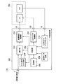
図を参照してONU100(光通信装置の具体例)は、LAN(ルータなど)や光電話器に接続する通信制御部104と、通信制御部104に接続される光トランシーバ106とを備えている。通信制御部104は、MAC_LSI(Media Access Control Large Scale Integration)を含む。光トランシーバ106は、一芯の光ファイバ114により、図示しない光カプラ(受動的光分岐ノード)を介してOLTに光学的に接続される。
Referring to the figure, ONU 100 (a specific example of an optical communication device) includes a
光トランシーバ106は、光受信機108と、光送信機110と、光合分波器112とを備えている。光受信機108は、光ファイバ114から光合分波器112を介して受信した光信号(下りフレーム)を電気信号に変換して通信制御部104に伝送する装置である。光送信機110は、通信制御部104から受信した電気信号を光信号(上りフレーム)に変換して、光合分波器112を介して光ファイバ114へ送る装置である。光送信機110は、入力端子I(入力部の一例)を介して通信制御部104から電気信号を入力し、光信号を光合分波器112へ出力する。
The
通信制御部104を構成する複数の電子部品と光トランシーバ106を構成する複数の電子部品とは、1枚の共通の基板102上に実装される。すなわち本実施の形態においては、光トランシーバ106はパッケージ化されておらず、光トランシーバ106と通信制御部104とを容易に着脱することができない。基板102において、光トランシーバ106が調整検査モードで動作することにより、ある温度におけるレーザダイオード駆動用の好ましい変調電流Imodとバイアス電流Ibiasとが算出される。算出された好ましい変調電流Imodとバイアス電流Ibiasとが、光トランシーバ106に設定される(光トランシーバ106の調整が行われる)。
A plurality of electronic components constituting the
従来は、通信制御部104と光トランシーバ106とは別部品として製造され、光トランシーバ106を調整した上で通信制御部104と光トランシーバ106とが接続されていた。本実施の形態では調整検査モードの存在により、通信制御部104と光トランシーバ106とを一体とした回路基板を採用しても、光トランシーバ106の調整が可能である。このため、ONU100を構成する部品点数を削減することができ、ONU100の低コスト化を図ることができる。
Conventionally, the
図2は、図1の光送信機110の構成を示すブロック図である。
FIG. 2 is a block diagram showing a configuration of the
図を参照して光送信機110は、レーザ駆動回路200(発光素子駆動装置の一例)と、TOSA(Transmitter Optical Subassembly)250とから構成される。
Referring to the drawing, the
TOSA250は、レーザダイオードLD(発光素子の一例)とフォトダイオードPD(検出部の一例)とを含んでいる。フォトダイオードPDは、レーザダイオードLDが出力する光をモニタするためのダイオードである。半導体レーザであれば、PN接合部から発生しレーザダイオードLDのある方向から出力された光が、レンズを介して光合分波器112(図1)側に送られる。レーザダイオードの他の方向から出力される光がフォトダイオードPDに入力され、発光強度や発光特性がモニタされる。
The
レーザダイオードLDと光ファイバ114との間には光合分波器112(図1)が設けられる。光合分波器112を介して光ファイバ114と光送信機110、および光ファイバ114と光受信機108がそれぞれ光学的に接続される。
An optical multiplexer / demultiplexer 112 (FIG. 1) is provided between the laser diode LD and the
レーザ駆動回路200は、レーザ駆動回路200を制御する制御部(CPU)202と、温度モニタ回路204(サーミスタを含む。)と、EEPROMなどから構成される記録部206と、マーク率の異なるテスト信号(検査用信号の一例)を出力することが可能なテスト信号出力回路208(出力部の一例)と、入力端子Iから入力した通信制御部104からの送信電気信号、またはテスト信号出力回路208からのテスト信号のいずれか一方を選択して出力する選択部(セレクタ)210と、選択部210の出力に基づいて、レーザダイオードLDを駆動するための変調電流を制御する変調電流制御部212(電流制御部の一例)と、レーザダイオードLDを駆動するためのバイアス電流を制御するLDバイアス制御部214と、フォトダイオードPDからの電気信号をモニタし、フォトダイオードPDの受光量を制御部202へ送るLD光出力パワーモニタ216(電流電圧変換回路を含む。)とを備えている。
The
レーザ駆動回路200においては、入力端子Iから送信電気信号が入力される。また、入力端子I3からフォトダイオードPDの検出信号が入力される。出力端子O1からレーザダイオードLDに変調電流が出力され、出力端子O2からレーザダイオードLDにバイアス電流が出力される。変調電流とバイアス電流との合計が、レーザダイオードLDの駆動電流となる。
In the
制御部202は、レーザ駆動回路200の現在のモードが通常動作モードであるときには、送信電気信号が選択部210から出力されるように、選択部210へ制御信号を送る。一方制御部202は、レーザ駆動回路200の現在のモードが調整検査モードであるときには、テスト信号が選択部210から出力されるように、選択部210へ制御信号を送る。また制御部202は、レーザ駆動回路200の現在のモードが調整検査モードであるときには、テスト信号のマーク率を指定するための信号をテスト信号出力回路208へ送る。テスト信号出力回路208は、指定されたマーク率の信号を出力する。
When the current mode of the
ここにマーク率とは、ある時間内のデジタル信号「1」の占める時間の割合をいう。ある時間中に常に「0」が伝送されるとき、マーク率は0(0%)である。ある時間中に常に「1」が伝送されるとき、マーク率は1(100%)である。ある時間内に「1」と「0」が伝送される頻度が同じであればマーク率は0.5(50%)となる。 Here, the mark rate refers to the proportion of the time occupied by the digital signal “1” within a certain time. When “0” is always transmitted during a certain time, the mark rate is 0 (0%). When “1” is always transmitted during a certain time, the mark rate is 1 (100%). If the frequency at which “1” and “0” are transmitted within a certain time is the same, the mark rate is 0.5 (50%).
より詳しくは調整検査モードにおいては、制御部202は第1のマーク率の信号を出力するようテスト信号出力回路208に対して要求を行い、これに応じてテスト信号出力回路208が第1のマーク率の信号を出力する。その後、制御部202は第2のマーク率の信号を出力するようテスト信号出力回路208に対して要求を行い、これに応じてテスト信号出力回路208が第2のマーク率の信号を出力する(さらにその後、制御部202が第3以降のマーク率の信号を出力するようテスト信号出力回路208に対して要求を行ってもよい)。
More specifically, in the adjustment inspection mode, the
またはテスト信号出力回路208が自律的に、それぞれが異なるマーク率を示す複数種類のテスト信号を出力することとしてもよい。すなわちテスト信号出力回路208が制御部202の指示によらず、第1のマーク率の信号、および第2のマーク率の信号(さらにその後、第3以降のマーク率の信号)を出力することとしてもよい。
Alternatively, the test
送信電気信号やテスト信号の品質を保つため、選択部210は、テスト信号出力回路208の出力ラインと入力端子Iからのラインとが電気的に接続されることがないよう構成されることが望ましい。また、通常動作モードが選択されている場合には、入力端子Iからのラインと変調電流制御部212の入力ラインとが電気的に接続され、テスト信号出力回路208の出力ラインは変調電流制御部212の入力ラインに電気的に接続されないように選択部210の回路を構成することが望ましい。同様に、調整検査モードが選択されている場合には、テスト信号出力回路208の出力ラインと変調電流制御部212の入力ラインとが電気的に接続され、入力端子Iからのラインは変調電流制御部212の入力ラインに電気的に接続されないように選択部210の回路を構成することが望ましい。このような構成により、テスト信号出力回路208を設けたことによる送信電気信号の品質劣化を防ぐことができる。調整検査モードにおいては、通信制御部104(図1)と光送信機110とを電気的に切り離すことができるため、テスト信号の品質を保つことができる。通常動作モードにおいては、テスト信号出力回路208と送信電気信号が流れるラインとを電気的に切り離すことができるため、送信電気信号の品質を保つことができる。
In order to maintain the quality of the transmission electrical signal and the test signal, the
制御部202は、調整検査モードの開始時、または通常動作モードにおいて、温度モニタ回路204の出力する光送信機110内の温度情報(またはレーザダイオードLDもしくはその近辺の温度情報)を、記録部206に記録されるテーブル(あるいは変換式)に基づいてバイアス電流Ibiasの値と変調電流Imodの値とに変換する。LDバイアス制御部214と変調電流制御部212とは、制御部202から出力されるバイアス電流Ibiasの値と変調電流Imodの値とに基づいて、レーザダイオードLDを駆動する。
At the start of the adjustment inspection mode or in the normal operation mode, the
制御部202は調整検査モードでの動作中において、LD光出力パワーモニタ216からの信号に基づいて、現在のレーザダイオードLDの発光特性を解析する。解析結果に基づき、温度モニタ回路204から把握される光送信機110内の温度(またはレーザダイオードLDもしくはその近辺の温度)X℃における、レーザダイオードLDの好ましいバイアス電流Ibiasの値と変調電流Imodの値とが求められる。求められたバイアス電流Ibiasの値と変調電流Imodの値とにより、記録部206のテーブルあるいは変換式が更新(上書き)される。更新されたテーブルあるいは変換式を用いて、それ以降のレーザダイオードLDの制御が行われる。
The
例えばテーブルを記録部206に記録する場合、更新においてテーブル内の温度X℃に対応する部分のみが書き換えられてもよい。または制御部202は、温度X℃における発光特性の解析結果と記録部206に記憶されているレーザダイオードLDの温度特性(これはテーブルでもよいし、計算式でもよい。)とから、X℃以外の温度におけるレーザダイオードLDの好ましいバイアス電流Ibiasの値と変調電流Imodの値とを演算し、それにより記録部206に記録されたテーブル内のX℃以外の温度に対応するバイアス電流Ibiasの値と変調電流Imodの値も更新してもよい。
For example, when the table is recorded in the
変換式を記録部206に記録する場合、現在の温度X℃でのレーザダイオードLDの好ましいバイアス電流Ibiasの値と変調電流Imodの値とに基づいて、変換式の変数(パラメータなど)が更新される。
When recording the conversion formula in the
このようにして、経年劣化によりレーザダイオードLDの特性が変化したとしても、記録部206内のデータを最新・最適なものにすることができる。
In this way, even if the characteristics of the laser diode LD change due to aging, the data in the
図3は、図1の光送信機110のより具体的な回路図である。
FIG. 3 is a more specific circuit diagram of the
実際のレーザ駆動回路200において、通信制御部104からの送信電気信号は、差動信号を伝送する2本のラインによって送られる。すなわち2本のラインの一方がHIGHレベルであるとき他方はLOWレベルであり、一方がLOWレベルであるとき他方はHIGHレベルである。差動信号として送信電気信号を伝送することで、雑音に対する送信電気信号の耐性を高めることが出来る。2本のラインからの送信電気信号は、入力端子I1,I2(図1および2ではこれらをまとめて入力端子Iと記載している。)からレーザ駆動回路200に入力される。入力端子I1,I2からの送信電気信号は、選択部210に入力される。入力端子I1,I2が選択部210に繋がる2本のラインのそれぞれには、インピーダンスマッチング用の抵抗R1,R2を介して電源VTが接続されている。
In the actual
テスト信号出力回路208も入力端子I1,I2と同様に、2本のラインによって差動信号を選択部210へ出力する。
Similarly to the input terminals I1 and I2, the test
変調電流制御部212は、選択部210の2本の差動出力ラインに接続されるバッファ回路226(ここでは増幅度が「1」のボルテージフォロア回路を示す。)と、バッファ回路226の2本の差動出力ライン各々に、それぞれのベース電極が接続されるトランジスタTr1,Tr2と、トランジスタTr1,Tr2のコレクタ電極に一端が接続され、他端が電源Vccに接続される抵抗R3,R4と、トランジスタTr1,Tr2のエミッタ電極にその一端が接続され、他端が接地電位に接続される変調電流源222とから構成される。
The modulation
トランジスタTr1,Tr2、抵抗R3,R4、および変調電流源222により、前段から送られた差動信号の差に比例した信号を出力する差動増幅回路が構成されている。差動増幅回路の出力端は、抵抗R3とトランジスタTr1とを繋ぐライン上のノードN1、および抵抗R4とトランジスタTr2とを繋ぐライン上のノードN2である。ノードN1およびノードN2が、図2で示した変調電流制御部212の出力端子O1に対応する。
The transistors Tr1 and Tr2, resistors R3 and R4, and the modulation
変調電流源222は、トランジスタTr1,Tr2を流れる電流の合計を決定する。差動増幅回路の出力は、トランジスタTr1,Tr2を流れる電流のバランス(および変調電流源222が流す電流)によって決定される。制御部(CPU)202が変調電流源222を制御することで、レーザダイオードLDの変調電流Imodが決定される。
The modulation
ノードN1,N2、LDバイアス制御部214、およびレーザダイオードLDを結ぶ2本のラインが、レーザダイオードLDに流れる電流を制御するラインとなる。この2本のラインは、各構成要素を直流結合(DC−Coupled)するラインで構成されている。これによりマーク率0%、100%の直流信号であっても、マーク率50%などの交流信号であっても、変調電流制御部212からレーザダイオードLDまで伝送することが可能である。
Two lines connecting the nodes N1 and N2, the LD
LDバイアス制御部214は、ノードN1,N2のそれぞれにDC結合されるノードN3,N4と、ノードN3に一端が接続され、他端が電源Vccに接続されるフェライトビーズ(またはコイル)FB1と、ノードN4にフェライトビーズ(またはコイル)FB2を介してその一端が接続されるバイアス電流源224とを備えている。バイアス電流源224の他端は、接地電位に接続される。レーザダイオードLDは、ノードN3,N4間に接続される。
制御部(CPU)202がバイアス電流源224を制御することで、レーザダイオードLDのバイアス電流Ibiasが決定される。
The control unit (CPU) 202 controls the bias
なおバッファ回路226は、レーザ駆動回路200の安定化のために用いられているものであり、省略することも可能である。
The
図3の回路において例えば、VT=2.25V、R1=R2=50Ω、R3=R4=25Ωとされる。 In the circuit of FIG. 3, for example, VT = 2.25V, R1 = R2 = 50Ω, and R3 = R4 = 25Ω.
以上説明した回路は、以下のように動作する。 The circuit described above operates as follows.
選択部210は、入力端子I1,I2からの差動信号を(バッファ回路226を介して)それぞれ後段のトランジスタTr1,Tr2のゲート電極に出力するか、テスト信号出力回路208の2本のラインからの差動信号を(バッファ回路226を介して)それぞれ後段のトランジスタTr1,Tr2のゲート電極に出力するかを、制御部(CPU)202の出力に基づいて決定する。通常動作モードでは制御部202が選択部210に制御信号を送ることで、入力端子I1,I2からの信号がバッファ回路226に出力されるようになる。
The
通常動作モードにおいて入力端子I1がHIGHレベル、入力端子I2がLOWレベルであるとき、トランジスタTr1はオンとなり、トランジスタTr2はオフとなる。これによりレーザダイオードLDにはバイアス電流Ibiasのみが流れ、レーザダイオードLDは弱い光しか出力しない。この状態は、レーザダイオードLDがLOWレベルの信号を伝送している状態(レーザダイオードLDの光パワーは「P0」)である。 In the normal operation mode, when the input terminal I1 is at the HIGH level and the input terminal I2 is at the LOW level, the transistor Tr1 is turned on and the transistor Tr2 is turned off. As a result, only the bias current Ibias flows through the laser diode LD, and the laser diode LD outputs only weak light. This state is a state in which the laser diode LD is transmitting a LOW level signal (the optical power of the laser diode LD is “P0”).
通常動作モードにおいて入力端子I1がLOWレベル、入力端子I2がHIGHレベルであるとき、トランジスタTr1はオフとなり、トランジスタTr2はオンとなる。これによりレーザダイオードLDにはバイアス電流Ibias+変調電流Imodの電流が流れ、レーザダイオードLDは強い光を出力する。この状態は、レーザダイオードLDがHIGHレベルの信号を伝送している状態(レーザダイオードLDの光パワーは「P1」(但しP1>P0))である。 In the normal operation mode, when the input terminal I1 is at the LOW level and the input terminal I2 is at the HIGH level, the transistor Tr1 is turned off and the transistor Tr2 is turned on. As a result, a bias current Ibias + modulation current Imod flows through the laser diode LD, and the laser diode LD outputs strong light. This state is a state in which the laser diode LD transmits a HIGH level signal (the optical power of the laser diode LD is “P1” (where P1> P0)).
また、例えばマーク率50%の信号が変調電流制御部212に入力されるとき、時間で平均すると、レーザダイオードLDにはバイアス電流Ibias+(変調電流Imod/2)の電流が流れていることとなる。時間で平均したレーザダイオードLDの平均光パワーは、(P0+P1)/2である。
Further, for example, when a signal with a mark ratio of 50% is input to the modulation
調整検査モードでは制御部202が選択部210に制御信号を送ることで、テスト信号出力回路208からの信号がバッファ回路226に出力されるようになる。また制御部202は、テスト信号出力回路208に、出力するテスト信号のマーク率を選択するための信号を出力する。これに伴い調整検査モードでは、テスト信号出力回路208から2本のラインを介して、送信電気信号と同様の差動信号が出力される。
In the adjustment inspection mode, the
調整検査モードでのテスト信号出力回路208の出力は、以下のようになる。
The output of the test
制御部202からのマーク率選択信号がマーク率0%を示すとき、テスト信号出力回路208のプラス側の出力ラインは+2.3Vに固定され、マイナス側のラインは0Vに固定される。これによりトランジスタTr1はオンとなり、トランジスタTr2はオフとなる。これによりレーザダイオードLDにはバイアス電流Ibiasのみが流れ、レーザダイオードLDは弱い光しか出力しない。
When the mark rate selection signal from the
制御部202からのマーク率選択信号がマーク率100%を示すとき、テスト信号出力回路208のプラス側の出力ラインは0Vに固定され、マイナス側のラインは+2.3Vに固定される。これによりトランジスタTr1はオフとなり、トランジスタTr2はオンとなる。これによりレーザダイオードLDにはバイアス電流Ibias+変調電流Imodの電流が流れ、レーザダイオードLDは強い光を出力する。
When the mark ratio selection signal from the
制御部202からのマーク率選択信号がマーク率50%を示すとき、テスト信号出力回路208のプラス側の出力ラインとマイナス側の出力ラインからは2.3Vの交流信号(例えば10Gbpsの信号)が出力される。これによりトランジスタTr1とトランジスタTr2は交互にオン/オフを繰り返す。時間で平均すると、レーザダイオードLDにはバイアス電流Ibias+(変調電流Imod/2)の電流が流れていることとなる。
When the mark rate selection signal from the
図4は、記録部206内に記録されるテーブルの具体例を示す図である。
FIG. 4 is a diagram illustrating a specific example of a table recorded in the
ここではテーブルにより温度をバイアス電流Ibiasの値(バイアス電流Ibiasの大きさ)、および変調電流Imodの値(変調電流Imodの大きさ)に変換するものとする。すなわち、温度0℃〜70℃内の所定の温度のそれぞれに対応付けて、設定するバイアス電流Ibiasの値、および変調電流Imodが記録されている。温度が高くなるとレーザダイオードLDは発光強度が弱まる傾向にあるため、温度が上がるごとにバイアス電流Ibiasの値、および変調電流Imodの値が大きくなるようにテーブルは設定されている。 Here, the temperature is converted into the value of the bias current Ibias (the magnitude of the bias current Ibias) and the value of the modulation current Imod (the magnitude of the modulation current Imod) using a table. That is, the value of the bias current Ibias to be set and the modulation current Imod are recorded in association with each of the predetermined temperatures within the temperature of 0 ° C. to 70 ° C. Since the laser diode LD tends to have a weak emission intensity as the temperature increases, the table is set so that the value of the bias current Ibias and the value of the modulation current Imod increase as the temperature increases.
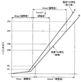
図5は、レーザダイオードLDを透過する電流値と、レーザダイオードLDの出力する光パワーとの関係を示す図である。 FIG. 5 is a diagram showing the relationship between the current value transmitted through the laser diode LD and the optical power output from the laser diode LD.
図のグラフにおいて、横軸がレーザダイオードLDを透過する電流値であり、縦軸がレーザダイオードLDの出力する光パワーを示している。図に示されるようにレーザダイオードLDを透過する電流が、「0」からある範囲内にあるときに、電流を変化させても出力される光パワーがあまり変わらない領域(不活性領域)がある。あるしきい値を電流が超えると、誘導放出が始まる領域(線形動作領域)となり、この領域においては電流の変化に合わせて光パワーが大きく変化する。通常動作モード、調整検査モードのいずれにおいてもレーザダイオードLDが線形動作領域で動作するよう、バイアス電流IbiasがレーザダイオードLDに付与される。変調電流Imodが流れていないとき、レーザダイオードLDに流れる電流はIbiasであり、そのときの光パワーはP0である。変調電流Imodが流れているとき、レーザダイオードLDに流れる電流はIbias+Imodであり、そのときの光パワーはP1である。光パワーP0と光パワーP1との違いにより、「0」または「1」のデジタル信号が伝達される。 In the graph of the figure, the horizontal axis represents the current value that passes through the laser diode LD, and the vertical axis represents the optical power output from the laser diode LD. As shown in the figure, when the current passing through the laser diode LD is within a certain range from “0”, there is a region (inactive region) where the output optical power does not change much even if the current is changed. . When the current exceeds a certain threshold value, a region where stimulated emission starts (linear operation region) is formed, and in this region, the optical power greatly changes in accordance with the change of the current. A bias current Ibias is applied to the laser diode LD so that the laser diode LD operates in the linear operation region in both the normal operation mode and the adjustment inspection mode. When the modulation current Imod does not flow, the current flowing through the laser diode LD is Ibias, and the optical power at that time is P0. When the modulation current Imod flows, the current flowing through the laser diode LD is Ibias + Imod, and the optical power at that time is P1. Depending on the difference between the optical power P0 and the optical power P1, a digital signal of “0” or “1” is transmitted.
図6は、レーザダイオードLDを駆動する信号のマーク率と、平均光パワーとの関係を示す図である。 FIG. 6 is a diagram showing the relationship between the mark ratio of the signal for driving the laser diode LD and the average optical power.
図6を参照してマーク率が0であるとき、レーザダイオードLDの光パワーは常にP0(図5)となるため、平均光パワーもP0となる。マーク率が1(100%)であるとき、レーザダイオードLDの光パワーは常にP1(図5)となるため、平均光パワーもP1となる。マーク率が0.5(50%)であるとき、レーザダイオードLDの光パワーはP0である期間が半分、P1である期間が半分となるため、平均光パワーは(P0+P1)/2となる。レーザダイオードLDの消光比は、P1/P0で表される。 Referring to FIG. 6, when the mark ratio is 0, the optical power of the laser diode LD is always P0 (FIG. 5), so the average optical power is also P0. When the mark ratio is 1 (100%), the optical power of the laser diode LD is always P1 (FIG. 5), so the average optical power is also P1. When the mark rate is 0.5 (50%), the optical power of the laser diode LD is half in the period P0 and half in the period P1, so the average optical power is (P0 + P1) / 2. The extinction ratio of the laser diode LD is represented by P1 / P0.
図7は、調整検査モードでの調整内容を説明するための図である。 FIG. 7 is a diagram for explaining the adjustment contents in the adjustment inspection mode.
図において横軸はレーザダイオードLDの透過電流を示し、縦軸はレーザダイオードLDの平均光パワーを示している。 In the figure, the horizontal axis indicates the transmission current of the laser diode LD, and the vertical axis indicates the average optical power of the laser diode LD.
ONU100導入時に記録部206に記録された、ある温度Tにおけるバイアス電流の値と変調電流の値がそれぞれIbias(調整前)、Imod(調整前)であったものとする。これは、レーザダイオードLDの導入時の特性が図7のAに示されるものであることによる。すなわち、温度TにおいてレーザダイオードLDを平均光パワーがPLからPHの範囲で発光させるために、Ibias(調整前)、Imod(調整前)が設定されている。例えば、マーク率50%の信号を出力する場合にレーザダイオードLDに付与される電流は、時間平均でIbias(調整前)+(Imod(調整前)/2)となる。このときの平均光パワーはPMである。
Assume that the bias current value and the modulation current value recorded at the
経時変化によって、温度TにおけるレーザダイオードLDの特性が図7のAからBに変化したものとする。すなわち、経時変化によってレーザダイオードLDの発光強度が低下した場合を想定している。 It is assumed that the characteristics of the laser diode LD at the temperature T change from A to B in FIG. That is, it is assumed that the light emission intensity of the laser diode LD is lowered due to the change over time.
レーザダイオードLDの特性が図7のAからBに変化すると、記録部206に従ってレーザダイオードLDに電流Ibias(調整前)、Imod(調整前)を付与したとき、レーザダイオードLDの平均光パワーは、PL’からPH’の範囲となり、導入時と比較して変化している。また、マーク率50%の場合の平均光パワーもPMからPM’に変化する。消光比も変化している。
When the characteristics of the laser diode LD change from A to B in FIG. 7, when currents Ibias (before adjustment) and Imod (before adjustment) are applied to the laser diode LD according to the
調整検査モードにおいては、このようなレーザダイオードLDの特性変化を補正するために、電流Ibias、およびImodの補正を行う。より詳しくは、温度がTであったとき、記録部206に記録されたIbias(調整前)、Imod(調整前)の値に従い、レーザダイオードLDが駆動される。マーク率0%、50%、100%のテスト信号がレーザダイオードLDに付与され、フォトダイオードPDによってレーザダイオードLDの平均光パワーが測定される。ここではそれぞれがPL’、PM’、PH’となる。
In the adjustment inspection mode, the currents Ibias and Imod are corrected in order to correct such a characteristic change of the laser diode LD. More specifically, when the temperature is T, the laser diode LD is driven according to the values of Ibias (before adjustment) and Imod (before adjustment) recorded in the
PL’、PM’、PH’の値とIbias(調整前)、Imod(調整前)の値とにより、現在のレーザダイオードLDの特性Bを得ることができる。レーザダイオードLDの特性Bに基づき、レーザダイオードLDを平均光パワーPLからPHの範囲で発光させるためのIbias’(調整後)、Imod’(調整後)を得ることができる。これらIbias’(調整後)、Imod’(調整後)の値に基づいて記録部206の記録データが更新され、次回からのレーザダイオードLDの駆動においては調整後の記録データが用いられる。
The current characteristic B of the laser diode LD can be obtained from the values of PL ′, PM ′, PH ′ and the values of Ibias (before adjustment) and Imod (before adjustment). Based on the characteristic B of the laser diode LD, Ibias '(after adjustment) and Imod' (after adjustment) for causing the laser diode LD to emit light in the range of the average optical power PL to PH can be obtained. The recording data of the
図8は、第1の実施の形態におけるONU100の制御部(CPU)202が調整検査モードにおいて実行する処理を示すフローチャートである。
FIG. 8 is a flowchart illustrating processing executed in the adjustment inspection mode by the control unit (CPU) 202 of the
制御部(CPU)202は、図8のフローチャートの処理を実行するプログラムに従って動作する。ONU100が調整検査モードに移行すると、ステップS101において制御部202は選択部210へ制御信号を送り、テスト信号出力回路208からの信号が変調電流制御部212へ出力されるようにする。ステップS103において制御部202は、温度モニタ回路204の出力に基づいて現在のONU100内の温度Tを測定する。ステップS105において制御部202は、記録部206内のテーブル(図4)を取得し、テーブルに基づいて、測定された温度TをIbias、Imodの値に変換する。制御部202は、変調電流源222、バイアス電流源224の電流がIbias、Imodとなるように、変調電流源222、バイアス電流源224へ制御信号を送る。
The control unit (CPU) 202 operates according to a program that executes the processing of the flowchart of FIG. When the
ステップS107において制御部202は、テスト信号出力回路208にマーク率0%のテスト信号を出力するよう、制御信号を送る。制御部202は、LD光出力パワーモニタ216からの信号に基づいてレーザダイオードLDの出力する平均光パワーを計測し、記憶する。
In step S107, the
ステップS109において制御部202は、テスト信号出力回路208にマーク率50%のテスト信号を出力するよう、制御信号を送る。制御部202は、LD光出力パワーモニタ216からの信号に基づいてレーザダイオードLDの出力する平均光パワーを計測し、記憶する。
In step S109, the
ステップS111において制御部202は、テスト信号出力回路208にマーク率100%のテスト信号を出力するよう、制御信号を送る。制御部202は、LD光出力パワーモニタ216からの信号に基づいてレーザダイオードLDの出力する平均光パワーを計測し、記憶する。
In step S111, the
ステップS113において制御部202は、ステップS107〜S111での測定結果に基づき、図7に示す現在の温度TにおけるレーザダイオードLDの特性と消光比とを求める。ステップS115において制御部202は、ステップS113で求められた現在のレーザダイオードLDの特性に従い、平均光パワーの最大値と最小値がPHとPLとになるような、温度TにおけるIbias’(調整後)、Imod’(調整後)を求める。また制御部202は、記録部206内に記憶されたレーザダイオードLDの温度特性に基づいて、温度T以外の温度におけるIbias’(調整後)、Imod’(調整後)を求める。
In step S113, the
ステップS117において制御部202は、ステップS115で求められた各温度におけるIbias’(調整後)、Imod’(調整後)を記録部206に上書きする。
In step S117, the
上記ステップS101、およびS107〜S111が、調整検査モードにおいて、それぞれマーク率が異なる複数種類の検査用信号に基づいてレーザダイオードLDに流れる電流を制御する制御ステップを構成している。 Steps S101 and S107 to S111 constitute a control step for controlling the current flowing through the laser diode LD based on a plurality of types of inspection signals having different mark rates in the adjustment inspection mode.
[第2の実施の形態]
以下、本発明の第2の実施の形態におけるONU100について、第1の実施の形態におけるONU100と異なる点を説明する。
[Second Embodiment]
Hereinafter, the difference between the
図9は、第2の実施の形態におけるONU100に用いられる光送信機110’の構成を示すブロック図である。
FIG. 9 is a block diagram illustrating a configuration of an
図2の光送信機110と比較して、図9の光送信機110’には、選択部210とテスト信号出力回路208とが設けられておらず、代わりに電圧制御部302が設けられている。入力端子Iから入力された送信電気信号は、電圧制御部302に入力される。電圧制御部302の出力は、変調電流制御部212に入力される。
Compared with the
図10は、図9の光送信機110’のより具体的な回路図である。
FIG. 10 is a more specific circuit diagram of the
図3の光送信機110と比較して、図10の光送信機110’では、入力端子I1,I2はそれぞれバッファ回路226に電気的に接続される。
Compared with the
制御部(CPU)202は、抵抗R5とフェライトビーズFB3とを介して、入力端子I1とバッファ回路226とを繋ぐラインに接続される。また制御部202は、抵抗R6とフェライトビーズFB4とを介して、入力端子I2とバッファ回路226とを繋ぐラインに接続される。これは、制御部202の電圧制御ラインVDAC1,VDAC2によって入力端子I1,I2とバッファ回路226とを繋ぐラインの電圧を制御するための構成(図9の電圧制御部302に相当)である。
The control unit (CPU) 202 is connected to a line connecting the input terminal I1 and the
フェライトビーズFB3,FB4は、高周波信号をブロック(遮断)し、低周波信号を通す性質を有する。これにより、入力端子I1,I2から入力される送信電気信号(高周波信号、交流成分)が制御部202側へ流れることが阻止される。結果として、通信制御部104からの送信電気信号(例えば10Gbpsの信号)の劣化が防止される。
Ferrite beads FB3 and FB4 have the property of blocking (blocking) high-frequency signals and allowing low-frequency signals to pass. This prevents transmission electrical signals (high-frequency signals, AC components) input from the input terminals I1 and I2 from flowing to the
調整検査モードにおいては、制御部202により電圧制御ラインVDAC1,VDAC2を介してバッファ回路226の入力端に、LOWレベルの信号またはHIGHレベルのテスト信号を入力することができる。すなわち第2の実施の形態では、第1の実施の形態で説明したテスト信号出力回路208の機能を制御部202が担うこととなる。フェライトビーズFB3,FB4を設けているため、バッファ回路226に入力可能なテスト信号は直流信号である。このため、第2の実施の形態のONU100におけるテスト信号のマーク率は、0%または100%とされている。
In the adjustment inspection mode, the
図10の回路において例えば、VT=2.25V、R1=R2=50Ω、R3=R4=25Ω、R5=R6=10Ωとされる。 In the circuit of FIG. 10, for example, VT = 2.25V, R1 = R2 = 50Ω, R3 = R4 = 25Ω, and R5 = R6 = 10Ω.
調整検査モードにおいてマーク率0%で検査を行うとき、電圧制御ラインVDAC1によって、入力端子I1とバッファ回路226とを繋ぐラインの電圧は+2.3Vに固定され、電圧制御ラインVDAC2によって、入力端子I2とバッファ回路226とを繋ぐラインの電圧は0Vに固定される。これによりトランジスタTr1はオンとなり、トランジスタTr2はオフとなる。レーザダイオードLDにはIbiasの電流のみが流れる。
When the inspection is performed at the mark rate of 0% in the adjustment inspection mode, the voltage of the line connecting the input terminal I1 and the
調整検査モードにおいてマーク率100%で検査を行うとき、電圧制御ラインVDAC1によって、入力端子I1とバッファ回路226とを繋ぐラインの電圧は0Vに固定され、電圧制御ラインVDAC2によって、入力端子I2とバッファ回路226とを繋ぐラインの電圧は+2.3Vに固定される。これによりトランジスタTr1はオフとなり、トランジスタTr2はオンとなる。レーザダイオードLDにはIbias+Imodの電流が流れる。
When the inspection is performed at the mark rate of 100% in the adjustment inspection mode, the voltage of the line connecting the input terminal I1 and the
図11は、第2の実施の形態におけるONU100の制御部(CPU)202が調整検査モードにおいて実行する処理を示すフローチャートである。
FIG. 11 is a flowchart illustrating processing executed in the adjustment inspection mode by the control unit (CPU) 202 of the
ステップS203〜S217からなる図11のフローチャートでは、図8のステップS101(選択部210の切替処理)、およびステップS109(マーク率50%のテスト信号の出力、光パワー取得処理)に相当する処理が省略されている。第2の実施の形態におけるONU100の調整では、マーク率0%のときの平均光パワー(図7におけるIbias(調整前)が流れたときの平均光パワー)と、マーク率100%のときの平均光パワー(図7におけるIbias(調整前)+Imod(調整前)が流れたときの平均光パワー)とが測定され(ステップS203〜S211)、その測定値によって温度Tにおける経時後のレーザダイオードLDの特性が求められる(ステップS213)。経時後のレーザダイオードLDの特性に基づいて、平均光パワーPH、PLを達成するためのIbias’(調整後)、Imod’(調整後)が求められ(ステップS215)、光送信機110の調整が行われる(ステップS217)。
In the flowchart of FIG. 11 including steps S203 to S217, processes corresponding to step S101 (switching process of the selection unit 210) and step S109 (output of a test signal with a mark rate of 50%, optical power acquisition process) of FIG. It is omitted. In the adjustment of the
なお第2の実施の形態において、フェライトビーズFB3,FB4を設けないことで、制御部202から交流信号をバッファ回路226に入力可能としてもよい。このようにすることで、0%および100%以外(例えば50%)のマーク率で調整検査を行うことができる。
In the second embodiment, an AC signal may be input from the
また、入力端子I1と通信制御部104との間の接続ライン、および入力端子I2と通信制御部104との間の接続ラインのそれぞれにコンデンサ(DCブロッキング・コンデンサ)を接続し、入力端子I1と通信制御部104、および入力端子I2と通信制御部104のそれぞれがAC結合されるように回路を構成することが望ましい。これにより、マーク率0%および100%のテスト信号(直流信号)が通信制御部104側に流れることが防止される。
Further, a capacitor (DC blocking capacitor) is connected to each of the connection line between the input terminal I1 and the
[通常動作モードにおける処理]
図12は、第1または第2の実施の形態におけるONU100の制御部(CPU)202が、通常動作モードにおいて実行する処理を示すフローチャートである。
[Processing in normal operation mode]
FIG. 12 is a flowchart showing processing executed in the normal operation mode by the control unit (CPU) 202 of the
図を参照して制御部(CPU)202は、図12のフローチャートの処理を実行するプログラムに従って動作する。 Referring to the figure, control unit (CPU) 202 operates according to a program that executes the processing of the flowchart of FIG.
ONU100が通常動作モードに移行すると、ステップS301において制御部202は選択部210へ制御信号を送り、入力端子Iからの信号が変調電流制御部212へ出力されるようにする(第1の実施の形態の場合のみ)。ステップS303において制御部202は、温度モニタ回路204の出力に基づいて現在のONU100内の温度Tを測定する。ステップS305において制御部202は、記録部206内のテーブル(図4)を取得し、テーブルに基づいて、測定された温度TをIbias、Imodの値に変換する。制御部202は、変調電流源222、バイアス電流源224の電流がIbias、Imodとなるように、変調電流源222、バイアス電流源224へ制御信号を送る。
When the
ステップS307においてONU100は、入力端子Iから入力された送信電気信号に基づいてレーザダイオードLDを駆動する。
In step S307, the
上記ステップS301およびS307が、通常動作モードにおいて、入力端子Iから入力した送信電気信号に基づいてレーザダイオードLDに流れる電流を制御する制御ステップを構成している。 Steps S301 and S307 constitute a control step for controlling the current flowing through the laser diode LD based on the transmission electric signal input from the input terminal I in the normal operation mode.
[実施の形態における効果]
以上のように構成された光送信機110、ならびにそれを用いた光トランシーバ106およびONU100によると、光送信機110内でマーク率0%、50%、100%など異なるマーク率のテスト信号を発生させることができ、それをレーザダイオードLDの調整検査に用いることができる。これにより別途調整検査のための機器を接続しなくても、調整検査を容易に行うことができる。
[Effects of the embodiment]
According to the
また装置が調整検査モードに入ると、自動で異なるマーク率のテスト信号を用いた検査が行われ、自動的に記録部206の内容が更新される。これにより熟練した技術を有しないユーザであっても正確な調整検査ができるというメリットがある。
When the apparatus enters the adjustment inspection mode, inspection using test signals with different mark ratios is automatically performed, and the contents of the
また、第1の実施の形態では選択部210を用いることで、通信制御部104と光送信機110との間の電気的接続をカットした上で、テスト信号出力回路208により光トランシーバ106の調整検査を行うことができる。これにより従来のように、光トランシーバ106の調整検査を行うために、光トランシーバ106を通信制御部104から取り外さなくてもよい。すなわち、1枚の共通の基板102上に通信制御部104を構成する電子部品と光トランシーバ106を構成する電子部品とを実装していても、光トランシーバ106の調整検査を行うことができる。また、1枚の共通の基板102上に通信制御部104を構成する電子部品と光トランシーバ106を構成する電子部品とを実装することで、ONU100の部品点数を削減することができる。
In the first embodiment, the
第2の実施の形態では、第1の実施の形態のように選択部210を設ける必要がなくなるため、レーザ駆動回路の規模を小さくすることができる。また第2の実施の形態では、フェライトビーズFB3,FB4により、通信制御部104からの信号を遮断することができるため、送信電気信号の品質を保つことが出来る。
In the second embodiment, since it is not necessary to provide the
[実施の形態の変形例]
なお上述の実施の形態では、本発明の発光素子駆動装置が光トランシーバ106およびそれを内蔵したONU100に用いられる例を示したが、本発明はこれに限られるものではなく、光送信を行う様々なデバイスに適用することができる。
[Modification of Embodiment]
In the above-described embodiment, the example in which the light-emitting element driving device of the present invention is used for the
また発光素子としてレーザダイオードLDを例に挙げたが、他の発光素子においても本発明を適用することができる。 Further, the laser diode LD is taken as an example of the light emitting element, but the present invention can be applied to other light emitting elements.
第1の実施の形態では異なるマーク率として、0%、50%、および100%(第2の実施の形態では、0%および100%)を例示したが、これに限らず他のマーク率を採用してもよい。但し、0%および100%のマーク率による調整検査を行うことで、レーザダイオードLDの特性をより正確に把握することができる。 In the first embodiment, examples of different mark rates are 0%, 50%, and 100% (in the second embodiment, 0% and 100%). However, the present invention is not limited to this. It may be adopted. However, the characteristics of the laser diode LD can be grasped more accurately by performing the adjustment inspection with the mark rates of 0% and 100%.
通常動作モードと調整検査モードとの切替え(選択)は、ユーザが図示しないスイッチを操作することで行われてもよいし、通常動作モードが所定時間実行されたのであれば、自動で調整検査モードでの動作を1回実行するなどしてもよい。また、OLTからの指示に従い、制御部202が通常動作モードと調整検査モードとの切替えを行うようにしてもよい。さらに、通常動作モードと調整検査モードだけでなく、発光素子駆動装置がさらに他のモード(第三のモード)を選択できるようにしてもよい。
Switching (selection) between the normal operation mode and the adjustment inspection mode may be performed by the user operating a switch (not shown). If the normal operation mode is executed for a predetermined time, the adjustment inspection mode is automatically performed. The operation in may be executed once. Further, the
図7におけるPH、PL、PMの測定処理は、測定誤差などを考慮して、数回測定を行った上での平均値を用いることが望ましい。 In the measurement processing of PH, PL, and PM in FIG. 7, it is desirable to use an average value after performing measurement several times in consideration of measurement errors and the like.
制御部(CPU)202を動作させるためのコンピュータの制御プログラムは、制御部(CPU)202内に記録されていてもよいし、記録部206内に記録されていてもよい。また、プログラムは外部記録メディアに記録され、図示しない入力端子からONU100内にインストールされてもよい。またはインターネット回線を通じてプログラムがONU100内にインストールされてもよい。プログラムは何らかの記憶部に記録され、コンピュータによって読み出されて実行されることで、コンピュータは動作する。
A computer control program for operating the control unit (CPU) 202 may be recorded in the control unit (CPU) 202 or may be recorded in the
上述の実施の形態は、すべての点で例示であって制限的なものではないと考えられるべきである。本発明の範囲は上記した説明ではなくて特許請求の範囲によって示され、特許請求の範囲と均等の意味および範囲内でのすべての変更が含まれることが意図される。 The above-described embodiment is to be considered as illustrative in all points and not restrictive. The scope of the present invention is defined by the terms of the claims, rather than the description above, and is intended to include any modifications within the scope and meaning equivalent to the terms of the claims.
100 ONU(光通信装置の一例)
102 1枚の基板
104 通信制御部
106 光トランシーバ
108 光受信機
110 光送信機
112 光合分波器
114 光ファイバ
200 レーザ駆動回路(発光素子駆動装置の一例)
202 制御部(CPU)
204 温度モニタ回路
206 記録部
208 テスト信号出力回路(出力部の一例)
210 選択部(セレクタ)
212 変調電流制御部(電流制御部の一例)
214 LDバイアス制御部
216 LD光出力パワーモニタ
222 変調電流源
224 バイアス電流源
226 バッファ回路
302 電圧制御部
LD レーザダイオード(発光素子の一例)
PD フォトダイオード(検出部の一例)
I,I1〜I3 入力端子(入力部の一例)
FB1〜FB4 フェライトビーズ
VDAC1,VDAC2 電圧制御ライン
100 ONU (an example of an optical communication device)
DESCRIPTION OF
202 Control unit (CPU)
204
210 Selector (Selector)
212 Modulation current control unit (an example of a current control unit)
214 LD
PD photodiode (example of detector)
I, I1-I3 input terminals (an example of an input unit)
FB1 to FB4 Ferrite beads VDAC1, VDAC2 Voltage control line
Claims (11)
送信電気信号を入力する入力部と、
発光素子に流れる電流を制御する電流制御部と、
それぞれマーク率が異なる複数種類の検査用信号を出力する出力部とを備え、
前記電流制御部は、
前記通常動作モードにおいて、前記入力部から入力した送信電気信号に基づいて前記発光素子に流れる電流を制御し、
前記調整検査モードにおいて、前記出力部が出力した、それぞれマーク率が異なる複数種類の検査用信号に基づいて、前記発光素子に流れる電流を制御する、発光素子駆動装置。 A light emitting element driving apparatus capable of selecting a normal operation mode and an adjustment inspection mode,
An input unit for inputting a transmission electric signal;
A current control unit for controlling a current flowing in the light emitting element;
An output unit that outputs a plurality of types of inspection signals each having a different mark rate,
The current controller is
In the normal operation mode, the current flowing through the light emitting element is controlled based on the transmission electrical signal input from the input unit,
In the adjustment inspection mode, a light-emitting element driving device that controls a current flowing through the light-emitting element based on a plurality of types of inspection signals output from the output unit and having different mark ratios.
前記出力部は、前記入力部と前記電流制御部との接続部分における電圧を制御する電圧制御部をさらに備え、
前記電圧制御部は、前記調整検査モードにおいて、前記入力部と前記電流制御部との接続部分における電圧を制御することで、それぞれマーク率が異なる複数種類の検査用信号を前記電流制御部に付与する、請求項1または2に記載の発光素子駆動装置。 The input unit and the current control unit are electrically connected,
The output unit further includes a voltage control unit that controls a voltage at a connection portion between the input unit and the current control unit,
In the adjustment inspection mode, the voltage control unit applies a plurality of types of inspection signals having different mark ratios to the current control unit by controlling a voltage at a connection portion between the input unit and the current control unit. The light emitting element drive device according to claim 1 or 2.
前記検出部の検出結果に基づいて、前記発光素子に流れる電流を調整する調整手段とをさらに備えた、請求項1から6のいずれかに記載の発光素子駆動装置。 In the adjustment inspection mode, a detection unit that detects light output from the light emitting element;
The light emitting element drive device according to claim 1, further comprising an adjusting unit that adjusts a current flowing through the light emitting element based on a detection result of the detection unit.
前記温度モニタ回路の出力に基づいて、前記発光素子に流れるバイアス電流の大きさと前記発光素子に流れる変調電流の大きさとを制御することを特徴とした、請求項1から7のいずれかに記載の発光素子駆動装置。 A temperature monitor circuit for detecting the temperature in the apparatus;
The magnitude of a bias current flowing through the light emitting element and a magnitude of a modulation current flowing through the light emitting element are controlled based on an output of the temperature monitor circuit. Light emitting element driving device.
請求項1から8のいずれかに記載された発光素子駆動装置、および前記発光素子駆動装置により駆動される発光素子を備えた光送信機と、
外部からの光信号を受信する光受信機とを含み、
前記通信制御部を構成する部品、前記光送信機を構成する部品、および前記光受信機を構成する部品は、1枚の基板上に実装される、光通信装置。 An optical communication device provided with a communication control unit,
A light-emitting element driving device according to any one of claims 1 to 8, and an optical transmitter including a light-emitting element driven by the light-emitting element driving device;
An optical receiver for receiving an optical signal from the outside,
An optical communication device in which a part constituting the communication control unit, a part constituting the optical transmitter, and a part constituting the optical receiver are mounted on a single substrate.
前記発光素子駆動装置は、
送信電気信号を入力する入力部と、
発光素子に流れる電流を制御する電流制御部と、
それぞれマーク率が異なる複数種類の検査用信号を出力する出力部とを備え、
前記制御方法は、
前記通常動作モードにおいて、前記入力部から入力した送信電気信号に基づいて前記発光素子に流れる電流を制御する第1の制御ステップと、
前記調整検査モードにおいて、前記出力部が出力した、それぞれマーク率が異なる複数種類の検査用信号に基づいて、前記発光素子に流れる電流を制御する第2の制御ステップとを備える、発光素子駆動装置の制御方法。 A method of controlling a light emitting element driving apparatus capable of selecting a normal operation mode and an adjustment inspection mode,
The light emitting element driving device includes:
An input unit for inputting a transmission electric signal;
A current control unit for controlling a current flowing in the light emitting element;
An output unit that outputs a plurality of types of inspection signals each having a different mark rate,
The control method is:
A first control step for controlling a current flowing through the light emitting element based on a transmission electrical signal input from the input unit in the normal operation mode;
A light emitting element driving device comprising: a second control step for controlling a current flowing through the light emitting element based on a plurality of types of inspection signals output from the output unit and having different mark rates in the adjustment inspection mode; Control method.
前記発光素子駆動装置は、
送信電気信号を入力する入力部と、
発光素子に流れる電流を制御する電流制御部と、
所定のマーク率の検査用信号を出力する出力部とを備え、
前記制御プログラムは、
前記通常動作モードにおいて、前記入力部から入力した送信電気信号に基づいて前記発光素子に流れる電流を制御する第1の制御ステップと、
前記調整検査モードにおいて、それぞれマーク率が異なる複数種類の検査用信号を前記出力部に出力させ、前記それぞれマーク率が異なる複数種類の検査用信号に基づいて、前記発光素子に流れる電流を制御する第2の制御ステップとをコンピュータに実行させる、発光素子駆動装置の制御プログラム。 A control program for a light emitting element driving apparatus capable of selecting a normal operation mode and an adjustment inspection mode,
The light emitting element driving device includes:
An input unit for inputting a transmission electric signal;
A current control unit for controlling a current flowing in the light emitting element;
An output unit that outputs an inspection signal having a predetermined mark ratio,
The control program is
A first control step for controlling a current flowing through the light emitting element based on a transmission electrical signal input from the input unit in the normal operation mode;
In the adjustment inspection mode, a plurality of types of inspection signals having different mark rates are output to the output unit, and a current flowing through the light emitting element is controlled based on the plurality of types of inspection signals having different mark rates. A control program for a light emitting element driving apparatus, causing a computer to execute the second control step.
Priority Applications (1)
| Application Number | Priority Date | Filing Date | Title |
|---|---|---|---|
| JP2012120986A JP2013247282A (en) | 2012-05-28 | 2012-05-28 | Light-emitting element driving device, optical communication device, light-emitting element driving device control method, and light-emitting element driving device control program |
Applications Claiming Priority (1)
| Application Number | Priority Date | Filing Date | Title |
|---|---|---|---|
| JP2012120986A JP2013247282A (en) | 2012-05-28 | 2012-05-28 | Light-emitting element driving device, optical communication device, light-emitting element driving device control method, and light-emitting element driving device control program |
Publications (1)
| Publication Number | Publication Date |
|---|---|
| JP2013247282A true JP2013247282A (en) | 2013-12-09 |
Family
ID=49846826
Family Applications (1)
| Application Number | Title | Priority Date | Filing Date |
|---|---|---|---|
| JP2012120986A Pending JP2013247282A (en) | 2012-05-28 | 2012-05-28 | Light-emitting element driving device, optical communication device, light-emitting element driving device control method, and light-emitting element driving device control program |
Country Status (1)
| Country | Link |
|---|---|
| JP (1) | JP2013247282A (en) |
Cited By (1)
| Publication number | Priority date | Publication date | Assignee | Title |
|---|---|---|---|---|
| JP2018195704A (en) * | 2017-05-17 | 2018-12-06 | 富士通株式会社 | Drive circuit, optical transmission module employing the same, and optical transmission device |
-
2012
- 2012-05-28 JP JP2012120986A patent/JP2013247282A/en active Pending
Cited By (1)
| Publication number | Priority date | Publication date | Assignee | Title |
|---|---|---|---|---|
| JP2018195704A (en) * | 2017-05-17 | 2018-12-06 | 富士通株式会社 | Drive circuit, optical transmission module employing the same, and optical transmission device |
Similar Documents
| Publication | Publication Date | Title |
|---|---|---|
| US7386020B2 (en) | Systems, devices and methods for temperature-based control of laser performance | |
| US6947455B2 (en) | Maintaining desirable performance of optical emitters at extreme temperatures | |
| US8855484B2 (en) | Method for controlling optical power and extinction ratio over entire temperature range | |
| US8483580B2 (en) | Method and apparatus for adjusting the gain of an amplifier of an optical receiver module based on link bit error rate (BER) measurements | |
| US8094692B2 (en) | Modulation method, modulation program, recording medium, modulation device, and optical transmitter | |
| JP2018125740A (en) | Optical transmitter-receiver and optical transmission-reception system | |
| CN102662105B (en) | Circuit, framework, apparatus and method for determining AC or DC bias in AC coupling signals | |
| TWI292486B (en) | Optic module calibration using an enhanced golden module | |
| JP2017532909A (en) | Method for determining receiver coupling efficiency, link margin and link topology in active optical cables | |
| CN103067090A (en) | Receiving signal power reinforcing indicator used for optical device and application method | |
| US20140029635A1 (en) | Laser power control using bias and modulation current feedback | |
| US8155159B2 (en) | Method and apparatus for calibrating burst mode laser transmitters | |
| US7400662B2 (en) | Calibration of laser systems | |
| JP2007194365A (en) | Optical transmission circuit | |
| US7411986B2 (en) | Optical system laser driver with a built in output inductor for improved frequency response | |
| US20060285563A1 (en) | Optical apparatus | |
| US7830936B2 (en) | Calibration of laser systems | |
| CN108011671B (en) | Method of controlling a semiconductor optical device comprising a semiconductor optical amplifier | |
| US20170373651A1 (en) | Trans-impedance amplifier arrangement and control module | |
| JP2013247282A (en) | Light-emitting element driving device, optical communication device, light-emitting element driving device control method, and light-emitting element driving device control program | |
| KR20060051503A (en) | Method and apparatus for distortion control for optical transmitters | |
| US20230379060A1 (en) | Optical transmitter | |
| JP6400235B1 (en) | Optical transmission device and optical transmission method | |
| US9306674B1 (en) | Field-tunable devices for optical communication | |
| JP2009168833A (en) | Bias circuit of external modulator |