JP2013221883A - Sample analysis element and detector - Google Patents
Sample analysis element and detector Download PDFInfo
- Publication number
- JP2013221883A JP2013221883A JP2012094519A JP2012094519A JP2013221883A JP 2013221883 A JP2013221883 A JP 2013221883A JP 2012094519 A JP2012094519 A JP 2012094519A JP 2012094519 A JP2012094519 A JP 2012094519A JP 2013221883 A JP2013221883 A JP 2013221883A
- Authority
- JP
- Japan
- Prior art keywords
- metal
- sample analysis
- light
- wavelength
- pitch
- Prior art date
- Legal status (The legal status is an assumption and is not a legal conclusion. Google has not performed a legal analysis and makes no representation as to the accuracy of the status listed.)
- Withdrawn
Links
Images


Classifications
-
- G—PHYSICS
- G01—MEASURING; TESTING
- G01N—INVESTIGATING OR ANALYSING MATERIALS BY DETERMINING THEIR CHEMICAL OR PHYSICAL PROPERTIES
- G01N21/00—Investigating or analysing materials by the use of optical means, i.e. using sub-millimetre waves, infrared, visible or ultraviolet light
- G01N21/17—Systems in which incident light is modified in accordance with the properties of the material investigated
- G01N21/55—Specular reflectivity
- G01N21/552—Attenuated total reflection
- G01N21/553—Attenuated total reflection and using surface plasmons
-
- G—PHYSICS
- G01—MEASURING; TESTING
- G01N—INVESTIGATING OR ANALYSING MATERIALS BY DETERMINING THEIR CHEMICAL OR PHYSICAL PROPERTIES
- G01N21/00—Investigating or analysing materials by the use of optical means, i.e. using sub-millimetre waves, infrared, visible or ultraviolet light
- G01N21/62—Systems in which the material investigated is excited whereby it emits light or causes a change in wavelength of the incident light
- G01N21/63—Systems in which the material investigated is excited whereby it emits light or causes a change in wavelength of the incident light optically excited
- G01N21/65—Raman scattering
- G01N21/658—Raman scattering enhancement Raman, e.g. surface plasmons
-
- B—PERFORMING OPERATIONS; TRANSPORTING
- B82—NANOTECHNOLOGY
- B82Y—SPECIFIC USES OR APPLICATIONS OF NANOSTRUCTURES; MEASUREMENT OR ANALYSIS OF NANOSTRUCTURES; MANUFACTURE OR TREATMENT OF NANOSTRUCTURES
- B82Y30/00—Nanotechnology for materials or surface science, e.g. nanocomposites
-
- G—PHYSICS
- G01—MEASURING; TESTING
- G01N—INVESTIGATING OR ANALYSING MATERIALS BY DETERMINING THEIR CHEMICAL OR PHYSICAL PROPERTIES
- G01N21/00—Investigating or analysing materials by the use of optical means, i.e. using sub-millimetre waves, infrared, visible or ultraviolet light
- G01N21/17—Systems in which incident light is modified in accordance with the properties of the material investigated
- G01N21/55—Specular reflectivity
- G01N21/552—Attenuated total reflection
- G01N21/553—Attenuated total reflection and using surface plasmons
- G01N21/554—Attenuated total reflection and using surface plasmons detecting the surface plasmon resonance of nanostructured metals, e.g. localised surface plasmon resonance
-
- G—PHYSICS
- G01—MEASURING; TESTING
- G01N—INVESTIGATING OR ANALYSING MATERIALS BY DETERMINING THEIR CHEMICAL OR PHYSICAL PROPERTIES
- G01N2201/00—Features of devices classified in G01N21/00
- G01N2201/06—Illumination; Optics
- G01N2201/061—Sources
- G01N2201/06113—Coherent sources; lasers
-
- Y—GENERAL TAGGING OF NEW TECHNOLOGICAL DEVELOPMENTS; GENERAL TAGGING OF CROSS-SECTIONAL TECHNOLOGIES SPANNING OVER SEVERAL SECTIONS OF THE IPC; TECHNICAL SUBJECTS COVERED BY FORMER USPC CROSS-REFERENCE ART COLLECTIONS [XRACs] AND DIGESTS
- Y10—TECHNICAL SUBJECTS COVERED BY FORMER USPC
- Y10T—TECHNICAL SUBJECTS COVERED BY FORMER US CLASSIFICATION
- Y10T428/00—Stock material or miscellaneous articles
- Y10T428/249921—Web or sheet containing structurally defined element or component
Landscapes
- Chemical & Material Sciences (AREA)
- Engineering & Computer Science (AREA)
- Health & Medical Sciences (AREA)
- General Physics & Mathematics (AREA)
- Physics & Mathematics (AREA)
- Nanotechnology (AREA)
- Pathology (AREA)
- General Health & Medical Sciences (AREA)
- Biochemistry (AREA)
- Immunology (AREA)
- Life Sciences & Earth Sciences (AREA)
- Analytical Chemistry (AREA)
- Nuclear Medicine, Radiotherapy & Molecular Imaging (AREA)
- Composite Materials (AREA)
- Condensed Matter Physics & Semiconductors (AREA)
- Materials Engineering (AREA)
- Crystallography & Structural Chemistry (AREA)
- Investigating, Analyzing Materials By Fluorescence Or Luminescence (AREA)
- Investigating Or Analysing Materials By Optical Means (AREA)
Abstract
Description
本発明は、金属ナノ粒子や金属ナノ突起といった金属ナノ体を備える試料分析素子、および、そうした試料分析素子を利用した検出装置等に関する。 The present invention relates to a sample analysis element including a metal nanobody such as a metal nanoparticle or a metal nanoprotrusion, a detection apparatus using the sample analysis element, and the like.
局在表面プラズモン共鳴(LSPR)を利用した試料分析素子は知られる。こうした試料分析素子は例えば誘電体表面に分散する金属ナノ体すなわち金属ナノ粒子を備える。金属ナノ粒子は例えば励起光の波長よりも十分に小さく形成される。金属ナノ粒子に励起光が照射されると、全電気双極子が揃い増強電場が誘発される。その結果、金属ナノ粒子の表面で近接場光が生成される。いわゆるホットスポットが形成される。 Sample analysis elements using localized surface plasmon resonance (LSPR) are known. Such a sample analysis element includes, for example, metal nano-particles or metal nanoparticles dispersed on a dielectric surface. For example, the metal nanoparticles are formed sufficiently smaller than the wavelength of the excitation light. When the metal nanoparticles are irradiated with excitation light, all electric dipoles are aligned and an enhanced electric field is induced. As a result, near-field light is generated on the surface of the metal nanoparticles. A so-called hot spot is formed.
非特許文献1では金属ナノ粒子は所定のピッチで格子状に配置される。ピッチの大きさが特定の数値に設定されると、エバネッセント波に基づき伝播表面プラズモン共鳴(PSPR)が引き起こされる。伝播表面プラズモン共鳴は局在表面プラズモン共鳴に結合する。いわゆるハイブリッドモードが確立される。こうして局在表面プラズモン共鳴は伝播表面プラズモン共鳴で増強され、金属ナノ粒子の表面で近接場光は強められる。
In
前述の試料分析素子は標的物質の検出装置に利用されることができる。非特許文献1に開示されるように、伝播表面プラズモン共鳴を引き起こすエバネッセント波の波長でピッチが設定されると、誘電体表面上でホットスポットの面密度が著しく低下し、標的物質がなかなかホットスポットに付着することができない。
The above-described sample analysis element can be used in a target substance detection apparatus. As disclosed in
本発明の少なくとも1つの態様によれば、ホットスポットの面密度を高めつつ局在表面プラズモン共鳴に伝播表面プラズモン共鳴を結合させることができる試料分析素子は提供されることができる。 According to at least one aspect of the present invention, a sample analysis element capable of coupling propagation surface plasmon resonance to localized surface plasmon resonance while increasing the surface density of hot spots can be provided.
(1)本発明の一態様は、誘電体表面に、入射光の波長よりも小さい第1のピッチで1列に配列される複数の金属ナノ体を含む複数の金属ナノ体列を備え、前記複数の金属ナノ体列は、前記第1のピッチよりも大きい第2のピッチで並列に並べられる試料分析素子に関する。 (1) One embodiment of the present invention includes a plurality of metal nanobody rows including a plurality of metal nanobody bodies arranged in one row at a first pitch smaller than a wavelength of incident light on a dielectric surface, The plurality of metal nanobody arrays relates to a sample analysis element arranged in parallel at a second pitch larger than the first pitch.
入射光の働きで金属ナノ体では局在表面プラズモン共鳴が引き起こされる。金属ナノ体列のピッチ(第2のピッチ)の働きでエバネッセント波に基づき伝播表面プラズモン共鳴が引き起こされる。伝播表面プラズモン共鳴は局在表面プラズモン共鳴に結合する。いわゆるハイブリッドモードが確立される。こうして局在表面プラズモン共鳴は伝播表面プラズモン共鳴で増強され、金属ナノ体の表面で近接場光は強められる。いわゆるホットスポットが形成される。しかも、個々の金属ナノ体列内には複数の金属ナノ体が配置されることから、金属ナノ体単体が入射光に共鳴するピッチで配置される場合に比べて金属ナノ体の面密度は高められる。したがって、ホットスポットの面密度は高められる。 The action of incident light causes localized surface plasmon resonance in the metal nanobody. Propagation surface plasmon resonance is caused based on the evanescent wave by the action of the pitch (second pitch) of the metal nanobody array. Propagating surface plasmon resonance couples to localized surface plasmon resonance. A so-called hybrid mode is established. Thus, localized surface plasmon resonance is enhanced by propagating surface plasmon resonance, and near-field light is enhanced on the surface of the metal nanobody. A so-called hot spot is formed. In addition, since a plurality of metal nanobodies are arranged in each metal nanobody array, the surface density of the metal nanobodies is higher than when the metal nanobodies are arranged at a pitch that resonates with incident light. It is done. Therefore, the surface density of the hot spot is increased.
(2)前記金属ナノ体列同士の間には、金属ナノ体を含まない領域が形成されることができる。すなわち、誘電体表面と、誘電体表面に平行で金属ナノ体の頂上面に接する仮想平面とで仕切られる空間内では隣接する金属ナノ体列同士の間は絶縁体(空間を含む)で満たされる。言い換えると、当該空間内で隣接する金属ナノ体列同士の間から金属材料は排除される。 (2) Between the metal nanobody rows, a region not including the metal nanobody may be formed. That is, in a space partitioned by a dielectric surface and a virtual plane parallel to the dielectric surface and in contact with the top surface of the metal nanobody, the adjacent metal nanobody rows are filled with an insulator (including a space). . In other words, the metal material is excluded from between the metal nanobody rows adjacent in the space.
(3)試料分析素子は、金属膜と、前記金属膜の表面に広がって、前記誘電体表面を構成する誘電体とを備えることができる。金属膜の金属と金属ナノ体の金属との間でダイポールが同じ方向を向くと、局所的な電場共鳴が引き起こされ、金属ナノ体の表面で近接場光は強められる。同様に、金属膜の金属と金属ナノ体の金属との間でダイポールが反対向きに向くと、局所的な電場共鳴が引き起こされ、金属ナノ体の表面で近接場光は強められる。 (3) The sample analysis element may include a metal film and a dielectric that spreads on the surface of the metal film and constitutes the dielectric surface. When the dipole faces in the same direction between the metal of the metal film and the metal of the metal nanobody, local electric field resonance is caused, and the near-field light is enhanced on the surface of the metal nanobody. Similarly, when the dipole faces in the opposite direction between the metal of the metal film and the metal of the metal nanobody, local electric field resonance is caused and the near-field light is intensified at the surface of the metal nanobody.
(4)前記第2のピッチは、前記金属ナノ体で生じる局在表面プラズモン共鳴の共鳴波長よりも短い波長で反射率の1次極小値を確立し、かつ、局在共鳴プラズモン共鳴の共鳴波長よりも長い波長で1次よりも高次の極小値を確立する大きさに設定されることができる。このように第2のピッチが設定されると、特定の波長で反射率は著しく低減される。その結果、局在表面プラズモンに確実に伝播表面プラズモンが結合する。金属ナノ体の表面で確実に近接場光は強められる。 (4) The second pitch establishes a primary minimum value of reflectance at a wavelength shorter than the resonance wavelength of localized surface plasmon resonance generated in the metal nanobody, and the resonance wavelength of localized resonance plasmon resonance It can be set to a magnitude that establishes a minimum value higher than the first order at longer wavelengths. When the second pitch is set in this way, the reflectance is significantly reduced at a specific wavelength. As a result, the propagation surface plasmon is reliably bonded to the localized surface plasmon. Near-field light is reliably enhanced on the surface of the metal nanobody.
(5)以上のような試料分析素子は検出装置に組み込まれて使用されることができる。検出装置は、試料分析素子と、前記金属ナノ体列に向けて光を放出する光源と、前記光の照射に応じて前記金属ナノ体列から放射される光を検出する光検出器とを備えることができる。 (5) The sample analysis element as described above can be used by being incorporated in a detection apparatus. The detection device includes a sample analysis element, a light source that emits light toward the metal nanobody array, and a photodetector that detects light emitted from the metal nanobody array in response to the light irradiation. be able to.
以下、添付図面を参照しつつ本発明の一実施形態を説明する。なお、以下に説明する本実施形態は、特許請求の範囲に記載された本発明の内容を不当に限定するものではなく、本実施形態で説明される構成の全てが本発明の解決手段として必須であるとは限らない。 Hereinafter, an embodiment of the present invention will be described with reference to the accompanying drawings. The present embodiment described below does not unduly limit the contents of the present invention described in the claims, and all the configurations described in the present embodiment are essential as means for solving the present invention. Not necessarily.
(1)試料分析素子の構造
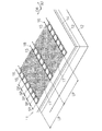
図1は本発明の一実施形態に係る試料分析素子11を概略的に示す。この試料分析素子11は基板12を備える。基板12は例えば誘電体から形成される。誘電体には例えばガラスが使用されることができる。
(1) Structure of Sample Analysis Element FIG. 1 schematically shows a
基板12の表面には金属膜13が形成される。金属膜13は金属から形成される。金属膜13は例えば金から形成されることができる。金属膜13は例えば基板12の表面に一面に途切れなく形成されることができる。金属膜13の膜厚は例えば100nm程度以上に設定されることができる。
A
金属膜13の表面には誘電膜(誘電体)14が形成される。誘電膜14は誘電体から形成される。誘電膜14は例えば二酸化シリコン(SiO2)といった酸化膜から形成されることができる。誘電膜14は例えば金属膜13の表面に全面に途切れなく形成されることができる。誘電膜14の膜厚は例えば40nm程度に設定されることができる。
A dielectric film (dielectric) 14 is formed on the surface of the
誘電膜14の表面には金属ナノ突起(金属ナノ体)15が形成される。金属ナノ突起15は誘電膜14の表面で分散する。金属ナノ突起15は金属から形成される。金属ナノ突起15は例えば銀から形成されることができる。その他、金属ナノ突起15の形成にあたって金またはアルミニウムが用いられてもよい。個々の金属ナノ突起15は角柱に形成される。角柱の水平断面は例えば正方形に形成される。正方形の一辺の長さは例えば1〜1000nm程度に設定されることができる。角柱の高さ(誘電膜の表面から)は例えば10〜100nm程度で設定されることができる。角柱の水平断面は正方形以外の多角形に形成されてもよい。金属ナノ突起15は円柱その他の立体形状に形成されてもよい。
Metal nanoprotrusions (metal nanobody) 15 are formed on the surface of the
金属ナノ突起15は金属ナノ突起列(金属ナノ体列)16を形成する。個々の金属ナノ突起列16内で金属ナノ突起15は短ピッチSP(第1のピッチ)で誘電膜14の表面に1列に配列される。金属ナノ突起列16は第1方向SDに延びる。短ピッチSPは入射光の波長よりも小さく設定される。
The metal nanoprotrusions 15 form a metal nanoprotrusion array (metal nanobody array) 16. In each
金属ナノ突起列16は第1方向SDに交差する第2方向DRに所定の長ピッチLP(第2のピッチ)で並列に並べられる。ここでは、第2方向DRは誘電膜14の表面を含む1仮想平面内で第1方向SDに直交する。長ピッチLPは少なくとも短ピッチSPよりも大きく設定される。望ましくは、長ピッチLPは、短ピッチSPで生じる局在プラズモン共鳴ピーク波長程度に設定される。長ピッチLPの大きさは、後述されるように、エバネッセント波の波数に応じて設定される。
The
金属ナノ突起列16同士の間には、金属ナノ突起を含まない非金属領域(金属ナノ体を含まない領域)17が形成される。すなわち、金属ナノ突起15の底面を含む仮想平面と、金属ナノ突起15の頂上面を含む仮想平面とに挟まれる空間内では隣接する金属ナノ突起列16同士の間は絶縁体(空間を含む)で満たされる。言い換えると、当該空間内で隣接する金属ナノ突起列16同士の間から金属材料は排除される。ここでは、金属ナノ突起列16同士の間では誘電膜14の表面が露出する。
Between the
試料分析素子11では、個々の金属ナノ突起15の大きさは入射光の波長よりも十分に小さく設定される。その結果、入射光の働きで金属ナノ突起15では局在表面プラズモン共鳴(LSPR)が引き起こされる。加えて、入射光の偏光面が第2方向DRに合わせ込まれると、長ピッチLPの設定に応じて、エバネッセント波に基づき伝播表面プラズモン共鳴(PSPR)が引き起こされる。伝播表面プラズモン共鳴は金属ナノ突起15の局在表面プラズモン共鳴に結合する。いわゆるハイブリッドモードが確立される。こうして局在表面プラズモン共鳴は伝播表面プラズモン共鳴で増強され、金属ナノ突起15の表面で近接場光は強められる。いわゆるホットスポットが形成される。しかも、個々の金属ナノ突起列16内では金属ナノ突起15同士の間隔は長ピッチLPよりも小さい短ピッチSPに設定されることから、金属ナノ突起15同士の間隔が長ピッチLPで設定される場合に比べて金属ナノ突起15の面密度は高められる。ホットスポットの面密度は高められる。
In the
この試料分析素子11では、長ピッチLPは、金属ナノ突起15で生じる局在表面プラズモン共鳴の共鳴波長よりも短い波長で反射率の1次極小値を確立し、かつ、局在共鳴プラズモン共鳴の共鳴波長よりも長い波長で1次よりも高次の極小値を確立する大きさに設定される。このように長ピッチLPが設定されると、特定の波長で反射率は著しく低減される。その結果、局在表面プラズモンに伝播表面プラズモンが確実に結合する。金属ナノ突起15の表面で確実に近接場光は強められる。
In the
(2)電場強度の検証
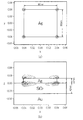
本発明者は試料分析素子11の電場強度を検証した。検証にあたってFDTD(Finite−Difference Time−Domain)法のシミュレーションソフトウェアが利用された。図2(a)および図2(b)に示されるように、本発明者はYee Cellに基づきシュミレーションモデルの単位ユニットを構築した。この単位ユニットでは120nm角の金属膜13が形成された。金属膜13には金が設定された。金属膜13上に誘電膜14が形成された。誘電膜14には二酸化シリコン(SiO2)が設定された。誘電膜14の膜厚は40nmに設定された。誘電膜14上に80nm角の金属ナノ突起15が形成された。金属ナノ突起15には銀が設定された。金属ナノ突起15の高さ(誘電膜14の表面から)は20nmに設定された。
(2) Verification of electric field strength The present inventors verified the electric field strength of the
図3(a)に示されるように、1列の単位ユニットすなわち金属ナノ突起15で1つの金属ナノ突起列16が構成された。複数の金属ナノ突起列16が平行に並べられた。x軸方向に金属ナノ突起列16の間に長ピッチLPが設定された。第1〜第7モデルでは長ピッチLPは240nm、360nm、480nm、550nmp、600nm、720nmおよび840nmにそれぞれ設定された。その結果、金属ナノ突起列16同士の間には1列の空隙単位ユニットで非金属領域17が形成された。空隙単位ユニットは120nm角の空隙で構成された。先頭の金属ナノ突起15で電場強度Exが算出された。周辺屈折率ns=1が設定された。直線偏光の入射光が設定された。偏光面はx軸方向に合わせられた。入射光は垂直入射に設定された。金属ナノ突起15では誘電膜14の表面に直交する稜線に沿って電場が集中した。
As shown in FIG. 3A, one row of unit units, ie,
図3(b)に示されるように、本発明者は第1比較モデルを用意した。第1比較モデルでは非金属領域17は省略された。すなわち、金属ナノ突起列16は設定されなかった。単純に金属ナノ突起15が短ピッチSPで格子状に配置された。前述と同様に、選択された1つの金属ナノ突起15で電場強度Exが算出された。同様に、図3(c)に示されるように、本発明者は第2比較モデルを用意した。第2比較モデルでは金属ナノ突起15同士の間に第1方向DRおよび第2方向SDにそれぞれ600nmのピッチが設定された。
As shown in FIG. 3B, the present inventor prepared a first comparison model. In the first comparative model, the
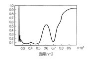
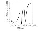
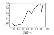
図4は第1比較モデルの反射率の波長依存性を示す。図5〜図11は第1〜第7モデルの反射率の波長依存性を示す。局所的な電場共鳴が起こると、反射率の低下が観察される。高い周波数で現れる極小値(1次極小値に相当)では金(Au)および銀(Ag)でダイポールが同じ方向に向くと考えられ、1次極小値よりも低い周波数で現れる極小値(1次よりも高い高次の極小値に相当)では金(Au)および銀(Ag)のダイポールが反対向きに向くと考えられる。図5および図6に示されるように、第1モデルおよび第2モデルでは波長683nmおよび696nm付近でそれぞれ2次極小値が観察された。図7〜9に示されるように、第3〜第5モデルでは波長555nm、590nmおよび620nmで1次極小値が観察され波長715nm、730nmおよび745nmで2次極小値が観察された。第3モデルでは波長715nmで反射率はほぼ「0(ゼロ)」を示した。第4モデルでは波長590nmおよび730nmでそれぞれ反射率はほぼ「0」に近づいた。第5モデルでは波長620nmで反射率はほぼ「0」を示した。 FIG. 4 shows the wavelength dependence of the reflectance of the first comparative model. 5 to 11 show the wavelength dependence of the reflectance of the first to seventh models. When local field resonance occurs, a decrease in reflectivity is observed. The minimum value that appears at a high frequency (corresponding to the primary minimum value) is considered that the dipole is oriented in the same direction with gold (Au) and silver (Ag), and the minimum value that appears at a frequency lower than the primary minimum value (primary value) (Corresponding to a higher high-order minimum), the gold (Au) and silver (Ag) dipoles are considered to face in opposite directions. As shown in FIGS. 5 and 6, in the first model and the second model, secondary minimum values were observed near wavelengths of 683 nm and 696 nm, respectively. As shown in FIGS. 7 to 9, in the third to fifth models, primary minimum values were observed at wavelengths of 555 nm, 590 nm, and 620 nm, and secondary minimum values were observed at wavelengths of 715 nm, 730 nm, and 745 nm. In the third model, the reflectance was substantially “0 (zero)” at a wavelength of 715 nm. In the fourth model, the reflectances approached “0” at wavelengths of 590 nm and 730 nm, respectively. In the fifth model, the reflectance was almost “0” at a wavelength of 620 nm.
図12は各モデルの反射率の極小値から作成された分散関係を示す。複数の長ピッチLPに共通に現れる波長(=683nm)は局在表面プラズモン共鳴の共鳴波長に相当する。なぜならば、分散関係の傾きは伝搬プラズモンの移動速度を示し、第1モデル(LP=240nm)で高次の極小値を示す角周波数の傾きは0(ゼロ)を示し、同様に、第6モデル(LP=720nm)および第7モデル(LP=840nm)で1次極小値を示す角周波数の傾きは0(ゼロ)を示すからである。局在表面プラズモン共鳴の共鳴波長は金属ナノ突起15の体積や誘電膜14の膜厚に応じて決定されることができる。また、各々の長ピッチLPごとに局在表面プラズモンの共鳴波長(=683nm)以外で反射率の極小値を示す波長は主に伝搬表面プラズモンと考えられる。単位面積当たりで金属ナノ突起15の並びが増加するにつれて金属ナノ突起15間の相互作用が増加し共鳴波長がレッドシフトつまり長波長側へシフトした結果である。共鳴ピーク波長の長波長化またはレッドシフトは金属ナノ突起15群間の相互作用の強さを示す。この波長683nmと金Au(ns=1)の伝播表面プラズモン共鳴の分散関係曲線とに基づき非特許文献1と同様にAnti−Crossing Behavior(ハイブリッドモードの指標として知られる)が観察された。
FIG. 12 shows the dispersion relation created from the minimum value of the reflectance of each model. The wavelength (= 683 nm) that appears in common in the plurality of long pitches LP corresponds to the resonance wavelength of localized surface plasmon resonance. This is because the slope of the dispersion relation indicates the moving speed of the propagation plasmon, the slope of the angular frequency indicating the high-order minimum value in the first model (LP = 240 nm) indicates 0 (zero), and similarly, the sixth model This is because the slope of the angular frequency indicating the primary minimum value in (LP = 720 nm) and the seventh model (LP = 840 nm) indicates 0 (zero). The resonance wavelength of localized surface plasmon resonance can be determined according to the volume of the metal nanoprotrusions 15 and the film thickness of the
図13は同様に電場強度Exの波長依存性を示す。ここでは、電場強度Exの最大値が特定された。最大値の算出にあたって第3〜第6モデル、第1比較モデルおよび第2比較モデルが用いられた。図13から明らかなように、第3〜第5モデルでは金属ナノ突起列16の形成に応じて第1比較モデルに比べて大きな最大値が観察された。特に、第4モデルおよび第5モデルは第1比較モデルおよび第2比較モデルに対して大きな最大値が観察された。このとき、第4モデルおよび第5モデルでは第2比較モデルに比べて金属ナノ突起15の面密度は高いことが認められる。第4モデルおよび第5モデルの長ピッチLPは、図8および図9から明らかなように、金属ナノ突起15で生じる局在表面プラズモン共鳴の共鳴波長よりも短い波長で反射率の1次極小値を確立し、かつ、局在共鳴プラズモン共鳴の共鳴波長よりも長い波長で1次よりも高次の極小値を確立する大きさに相当する。
FIG. 13 similarly shows the wavelength dependence of the electric field intensity Ex. Here, the maximum value of the electric field intensity Ex is specified. In calculating the maximum value, the third to sixth models, the first comparison model, and the second comparison model were used. As is clear from FIG. 13, in the third to fifth models, a larger maximum value was observed as compared to the first comparative model depending on the formation of the
(3)試料分析素子の製造方法
試料分析素子11は既知の製造方法で製造されることができる。すなわち、試料分析素子11の製造にあたってガラスウエハーが用意される。ガラスウエハーの表面には金膜および二酸化シリコン膜が順番に積層される。積層にあたって例えばめっき法やスパッタリング法が用いられればよい。二酸化シリコン膜の表面には一面に金属ナノ突起15の素材で積層膜が形成される。積層膜の表面には金属ナノ突起15を象ったマスクが形成される。マスクには例えばフォトレジストが用いられればよい。マスクの周囲で積層膜が除去されると、積層膜から個々の金属ナノ突起15は成形される。こうした成形にあたってエッチング処理やミリング処理が実施されればよい。ガラスウエハーから個々の基板12が切り出される。
(3) Method for Manufacturing Sample Analysis Element The
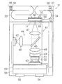
(4)一実施形態に係る検出装置
図14は一実施形態に係る標的分子検出装置(検出装置)31を概略的に示す。標的分子検出装置31はセンサーユニット32を備える。センサーユニット32には導入通路33と排出通路34とが個別に接続される。導入通路33からセンサーユニット32に気体は導入される。センサーユニット32から排出通路34に気体は排出される。導入通路33の通路入口35にはフィルター36が設置される。フィルター36は例えば気体中の塵埃や水蒸気を除去することができる。排出通路34の通路出口37には吸引ユニット38が設置される。吸引ユニット38は送風ファンで構成される。送風ファンの作動に応じて気体は導入通路33、センサーユニット32および排出通路34を順番に流通する。こうした気体の流通経路内でセンサーユニット32の前後にはシャッター(図示されず)が設置される。シャッターの開閉に応じてセンサーユニット32内に気体は閉じ込められることができる。
(4) Detection Device According to One Embodiment FIG. 14 schematically shows a target molecule detection device (detection device) 31 according to one embodiment. The target
標的分子検出装置31はラマン散乱光検出ユニット41を備える。ラマン散乱光検出ユニット41は、センサーユニット32に照射光を照射しラマン散乱光を検出する。ラマン散乱光検出ユニット41には光源42が組み込まれる。光源42にはレーザー光源が用いられることができる。レーザー光源は特定波長(単一波長)で直線偏光のレーザー光を放射することができる。
The target
ラマン散乱光検出ユニット41は受光素子43を備える。受光素子43は例えば光の強度を検出することができる。受光素子43は光の強度に応じて検出電流を出力することができる。したがって、受光素子43から出力される電流の大きさに応じて光の強度は特定されることができる。
The Raman scattered
光源42とセンサーユニット32との間、および、センサーユニット32と受光素子43との間には光学系44が構築される。光学系44は光源42とセンサーユニット32との間に光路を形成すると同時にセンサーユニット32と受光素子43との間に光路を形成する。光学系44の働きで光源42の光はセンサーユニット32に導かれる。センサーユニット32の反射光は光学系44の働きで受光素子43に導かれる。
An
光学系44はコリメーターレンズ45、ダイクロイックミラー46、対物レンズ47、集光レンズ48、凹レンズ49、光学フィルター51および分光器52を備える。ダイクロイックミラー46は例えばセンサーユニット32と受光素子43との間に配置される。対物レンズ47はダイクロイックミラー46とセンサーユニット32との間に配置される。対物レンズ47はダイクロイックミラー46から供給される平行光を集光してセンサーユニット32に導く。センサーユニット32の反射光は対物レンズ47で平行光に変換されダイクロイックミラー46を透過する。ダイクロイックミラー46と受光素子43との間には集光レンズ48、凹レンズ49、光学フィルター51および分光器52が配置される。対物レンズ47、集光レンズ48および凹レンズ49の光軸は同軸に合わせ込まれる。集光レンズ48で集光された光は凹レンズ49で再び平行光に変換される。光学フィルター51はレイリー散乱光を除去する。ラマン散乱光は光学フィルター51を通過する。分光器52は例えば特定波長の光を選択的に透過させる。こうして受光素子43では特定波長ごとに光の強度が検出される。分光器52には例えばエタロンが用いられることができる。
The
光源42の光軸は対物レンズ47および集光レンズ48の光軸に直交する。ダイクロイックミラー46の表面はこれら光軸に45度の角度で交差する。ダイクロイックミラー46と光源42との間にはコリメーターレンズ45が配置される。こうしてコリメーターレンズ45は光源42に向き合わせられる。コリメーターレンズ45の光軸は光源42の光軸に同軸に合わせ込まれる。
The optical axis of the
標的分子検出装置31は制御ユニット53を備える。制御ユニット53に、光源42、分光器52、受光素子43、吸引ユニット38、その他の機器が接続される。制御ユニット53は、光源42、分光器52および吸引ユニット38の動作を制御するとともに、受光素子43の出力信号を処理する。制御ユニット53には信号コネクター54が接続される。制御ユニット53は信号コネクター54を通じて外部と信号をやりとりすることができる。
The target
標的分子検出装置31は電源ユニット55を備える。電源ユニット55は制御ユニット53に接続される。電源ユニット55は制御ユニット53に動作電力を供給する。制御ユニット53は電源ユニット55から電力の供給を受けて動作することができる。電源ユニット55には例えば1次電池や2次電池が用いられることができる。2次電池は、例えば、充電用の電源コネクター56を有することができる。
The target
制御ユニット53は信号処理制御部を備える。信号処理制御部は例えば中央演算処理装置(CPU)と、RAM(ランダムアクセスメモリー)やROM(リードオンリーメモリー)といった記憶回路で構成されることができる。ROMには例えば処理プログラムやスペクトルデータが格納されることができる。スペクトルデータでは標的分子のラマン散乱光のスペクトルが特定される。CPUは、一時的にRAMに処理プログラムやスペクトルデータを取り込みながら、処理プログラムを実行する。CPUは、スペクトルデータに、分光器および受光素子の働きで特定される光のスペクトルを照らし合わせる。
The
センサーユニット32はセンサーチップ11を備える。センサーチップ11は基板58に向き合わせられる。センサーチップ11と基板58との間には気体室59が形成される。気体室59は一端で導入通路33に接続され他端で排出通路34に接続される。気体室59内に金属ナノ突起15が配置される。光源42から放出される光はコリメーターレンズ45で平行光に変換される。直線偏光の光はダイクロイックミラー46で反射する。反射した光は対物レンズ47で集光されてセンサーユニット32に照射される。このとき、光はセンサーチップ11の表面に直交する垂直方向に入射することができる。いわゆる垂直入射が確立されることができる。光の偏光面は凸筋14に平行に合わせ込まれる。照射された光の働きで金属ナノ突起15では局在表面プラズモン共鳴が引き起こされる。金属ナノ突起15同士の間で近接場光は強められる。いわゆるホットスポットが形成される。
The
このとき、ホットスポットで金属ナノ突起15に標的分子が付着すると、標的分子からレイリー散乱光およびラマン散乱光が生成される。いわゆる表面増強ラマン散乱が実現される。その結果、標的分子の種類に応じたスペクトルで光は対物レンズ47に向かって放出される。
At this time, when the target molecule adheres to the
こうしてセンサーユニット32から放出される光は対物レンズ47で平行光に変換されダイクロイックミラー46、集光レンズ48、凹レンズ49および光学フィルター51を通過する。ラマン散乱光は分光器52に入射する。分光器52はラマン散乱光を分光する。こうして特定の波長ごとに受光素子43は光の強度を検出する。光のスペクトルはスペクトルデータに照らし合わせられる。光のスペクトルに応じて標的分子は検出されることができる。こうして標的分子検出装置31は表面増強ラマン散乱に基づき例えばアデノウィルスやライノウィルス、HIVウィルス、インフルエンザウィルスといった標的物質を検出することができる。
Thus, the light emitted from the
なお、上記のように本実施形態について詳細に説明したが、本発明の新規事項および効果から実体的に逸脱しない多くの変形が可能であることは当業者には容易に理解できるであろう。したがって、このような変形例はすべて本発明の範囲に含まれる。例えば、明細書または図面において、少なくとも一度、より広義または同義な異なる用語とともに記載された用語は、明細書または図面のいかなる箇所においても、その異なる用語に置き換えられることができる。また、試料分析素子11や標的分子検出装置31等の構成および動作も本実施形態で説明したものに限定されず、種々の変形が可能である。
Although the present embodiment has been described in detail as described above, it will be easily understood by those skilled in the art that many modifications can be made without departing from the novel matters and effects of the present invention. Therefore, all such modifications are included in the scope of the present invention. For example, a term described with a different term having a broader meaning or the same meaning at least once in the specification or the drawings can be replaced with the different term in any part of the specification or the drawings. Further, the configurations and operations of the
11 試料分析素子、13 金属膜、14 誘電体(誘電膜)、15 金属ナノ体(金属ナノ突起)、16 金属ナノ体列(金属ナノ突起列)、17 金属ナノ体を含まない領域(非金属領域)、31 検出装置(標的分子検出装置)、42 光源、43 光検出器(受光素子)、LP 第2のピッチ(長ピッチ)、SP 第1のピッチ(短ピッチ)。 11 Sample analysis element, 13 Metal film, 14 Dielectric (dielectric film), 15 Metal nanobody (metal nanoprojection), 16 Metal nanobody array (metal nanoprojection array), 17 Region not containing metal nanobody (nonmetal) Area), 31 detector (target molecule detector), 42 light source, 43 photodetector (light receiving element), LP second pitch (long pitch), SP first pitch (short pitch).
Claims (5)
前記金属ナノ体列に向けて光を放出する光源と、
前記光の照射に応じて前記金属ナノ体列から放射される光を検出する光検出器と
を備えることを特徴とする検出装置。 The sample analysis element according to any one of claims 1 to 4,
A light source that emits light toward the metal nanobody array;
And a photodetector that detects light emitted from the metal nanobody array in response to the light irradiation.
Priority Applications (5)
| Application Number | Priority Date | Filing Date | Title |
|---|---|---|---|
| JP2012094519A JP2013221883A (en) | 2012-04-18 | 2012-04-18 | Sample analysis element and detector |
| US14/395,243 US9228944B2 (en) | 2012-04-18 | 2013-04-12 | Sample analysis element and detection device |
| EP13777779.3A EP2840383A4 (en) | 2012-04-18 | 2013-04-12 | Sample analysis element and detection device |
| PCT/JP2013/002503 WO2013157233A1 (en) | 2012-04-18 | 2013-04-12 | Sample analysis element and detection device |
| CN201380020394.0A CN104321639A (en) | 2012-04-18 | 2013-04-12 | Sample analysis element and detection device |
Applications Claiming Priority (1)
| Application Number | Priority Date | Filing Date | Title |
|---|---|---|---|
| JP2012094519A JP2013221883A (en) | 2012-04-18 | 2012-04-18 | Sample analysis element and detector |
Publications (2)
| Publication Number | Publication Date |
|---|---|
| JP2013221883A true JP2013221883A (en) | 2013-10-28 |
| JP2013221883A5 JP2013221883A5 (en) | 2015-06-11 |
Family
ID=49383205
Family Applications (1)
| Application Number | Title | Priority Date | Filing Date |
|---|---|---|---|
| JP2012094519A Withdrawn JP2013221883A (en) | 2012-04-18 | 2012-04-18 | Sample analysis element and detector |
Country Status (5)
| Country | Link |
|---|---|
| US (1) | US9228944B2 (en) |
| EP (1) | EP2840383A4 (en) |
| JP (1) | JP2013221883A (en) |
| CN (1) | CN104321639A (en) |
| WO (1) | WO2013157233A1 (en) |
Cited By (4)
| Publication number | Priority date | Publication date | Assignee | Title |
|---|---|---|---|---|
| JP2015215178A (en) * | 2014-05-08 | 2015-12-03 | セイコーエプソン株式会社 | Electric field enhancement element, analyzing device and electronic apparatus |
| US9389179B2 (en) | 2014-02-17 | 2016-07-12 | Seiko Epson Corporation | Analysis apparatus and electronic device |
| US9389178B2 (en) | 2013-03-05 | 2016-07-12 | Seiko Epson Corporation | Analysis device, analysis method, optical element and electronic apparatus for analysis device and analysis method, and method of designing optical element |
| JP2017514148A (en) * | 2014-04-08 | 2017-06-01 | インスプロリオン・センサー・システムズ・アーベー | Battery with sensor |
Families Citing this family (5)
| Publication number | Priority date | Publication date | Assignee | Title |
|---|---|---|---|---|
| WO2014097886A1 (en) * | 2012-12-18 | 2014-06-26 | 学校法人早稲田大学 | Optical device and analysis apparatus |
| JP2015055482A (en) * | 2013-09-10 | 2015-03-23 | セイコーエプソン株式会社 | Analysis device, analysis method, and optical element and electronic device used therein |
| JP6613736B2 (en) * | 2015-09-07 | 2019-12-04 | セイコーエプソン株式会社 | Substance detection method and substance detection apparatus |
| DE102017105113B4 (en) | 2017-03-10 | 2021-09-30 | Leibniz-Institut für Photonische Technologien e.V. (Engl.Leibniz Institute of Photonic Technology) | Arrangement and method for the detection of changes in the optical path length in a nano-capillary channel |
| US11959859B2 (en) * | 2021-06-02 | 2024-04-16 | Edwin Thomas Carlen | Multi-gas detection system and method |
Family Cites Families (39)
| Publication number | Priority date | Publication date | Assignee | Title |
|---|---|---|---|---|
| JP3452837B2 (en) | 1999-06-14 | 2003-10-06 | 理化学研究所 | Localized plasmon resonance sensor |
| JP4231701B2 (en) | 2002-01-08 | 2009-03-04 | 富士フイルム株式会社 | Plasmon resonance device |
| US7079250B2 (en) | 2002-01-08 | 2006-07-18 | Fuji Photo Film Co., Ltd. | Structure, structure manufacturing method and sensor using the same |
| JP3897703B2 (en) | 2002-01-11 | 2007-03-28 | キヤノン株式会社 | Sensor device and inspection method using the same |
| US7399445B2 (en) | 2002-01-11 | 2008-07-15 | Canon Kabushiki Kaisha | Chemical sensor |
| US7088449B1 (en) | 2002-11-08 | 2006-08-08 | The Board Of Trustees Of The Leland Stanford Junior University | Dimension measurement approach for metal-material |
| EP1445601A3 (en) | 2003-01-30 | 2004-09-22 | Fuji Photo Film Co., Ltd. | Localized surface plasmon sensor chips, processes for producing the same, and sensors using the same |
| JP3957199B2 (en) | 2003-03-19 | 2007-08-15 | 富士フイルム株式会社 | Sensor chip, method of manufacturing sensor chip, and sensor using the sensor chip |
| US7239076B2 (en) * | 2003-09-25 | 2007-07-03 | General Electric Company | Self-aligned gated rod field emission device and associated method of fabrication |
| AU2005246415B8 (en) | 2004-05-19 | 2011-09-01 | Vp Holding, Llc | Optical sensor with layered plasmon structure for enhanced detection of chemical groups by SERS |
| JP4156567B2 (en) * | 2004-06-16 | 2008-09-24 | 日本電信電話株式会社 | SPR sensor and refractive index measuring method |
| US7483130B2 (en) | 2004-11-04 | 2009-01-27 | D3 Technologies, Ltd. | Metal nano-void photonic crystal for enhanced Raman spectroscopy |
| JP2006208057A (en) | 2005-01-25 | 2006-08-10 | Taiyo Yuden Co Ltd | Plasmon resonance structure, its control method and manufacturing method of metal domain |
| WO2007083817A1 (en) | 2006-01-18 | 2007-07-26 | Canon Kabushiki Kaisha | Target substance-detecting element |
| JP2007218900A (en) | 2006-01-18 | 2007-08-30 | Canon Inc | Element for detecting target substance |
| JP2007240361A (en) | 2006-03-09 | 2007-09-20 | Sekisui Chem Co Ltd | Localized plasmon enhancing sensor |
| JP4994682B2 (en) | 2006-03-16 | 2012-08-08 | キヤノン株式会社 | Detection element, target substance detection apparatus using the detection element, and method for detecting target substance |
| JP5286515B2 (en) | 2006-05-11 | 2013-09-11 | 国立大学法人秋田大学 | Sensor chip and sensor chip manufacturing method |
| WO2007132795A1 (en) | 2006-05-12 | 2007-11-22 | Canon Kabushiki Kaisha | Detecting element, detecting device and detecting method |
| JP2008025989A (en) | 2006-07-15 | 2008-02-07 | Keio Gijuku | Ligand analyzing method due to localized surface plasmon resonance method and mass analyzing method, and sensor element therefor |
| GB2447696A (en) | 2007-03-23 | 2008-09-24 | Univ Exeter | Photonic biosensor arrays |
| US7768640B2 (en) | 2007-05-07 | 2010-08-03 | The Board Of Trustees Of The University Of Illinois | Fluorescence detection enhancement using photonic crystal extraction |
| JP5116362B2 (en) | 2007-05-28 | 2013-01-09 | 株式会社リコー | Biosensor |
| US7639355B2 (en) | 2007-06-26 | 2009-12-29 | Hewlett-Packard Development Company, L.P. | Electric-field-enhancement structure and detection apparatus using same |
| JP5080186B2 (en) | 2007-09-26 | 2012-11-21 | 富士フイルム株式会社 | Molecular analysis photodetection method, molecular analysis photodetection device used therefor, and sample plate |
| JP5294600B2 (en) | 2007-09-28 | 2013-09-18 | キヤノン株式会社 | Target substance detection device and target substance detection method |
| JP5288772B2 (en) * | 2007-11-02 | 2013-09-11 | キヤノン株式会社 | Chemical sensor element, sensing device, and sensing method |
| JP5175584B2 (en) | 2008-03-13 | 2013-04-03 | 地方独立行政法人 東京都立産業技術研究センター | Local surface plasmon resonance imaging system |
| JP5396761B2 (en) * | 2008-07-11 | 2014-01-22 | 株式会社リコー | LIGHT CONTROL ELEMENT HAVING MICROSTRUCTURE AND MICROSTRUCTURE |
| EP2362947B1 (en) | 2008-09-30 | 2017-05-10 | Pacific Biosciences of California, Inc. | Ultra-high multiplex analytical systems and methods |
| JP2010256161A (en) * | 2009-04-24 | 2010-11-11 | Konica Minolta Holdings Inc | Plasmon excitation sensor, and assay method using the same |
| US8259381B2 (en) * | 2009-06-05 | 2012-09-04 | Exelis Inc. | Phase-change materials and optical limiting devices utilizing phase-change materials |
| JP5621394B2 (en) | 2009-11-19 | 2014-11-12 | セイコーエプソン株式会社 | Sensor chip, sensor cartridge and analyzer |
| US8415611B2 (en) | 2009-11-19 | 2013-04-09 | Seiko Epson Corporation | Sensor chip, sensor cartridge, and analysis apparatus |
| JP5589656B2 (en) | 2009-12-11 | 2014-09-17 | セイコーエプソン株式会社 | Sensor chip, sensor cartridge and analyzer |
| US8467061B2 (en) | 2010-02-19 | 2013-06-18 | Pacific Biosciences Of California, Inc. | Integrated analytical system and method |
| EP2372348A1 (en) | 2010-03-22 | 2011-10-05 | Imec | Methods and systems for surface enhanced optical detection |
| EP2694949A1 (en) | 2011-04-05 | 2014-02-12 | Integrated Plasmonics Corporation | Integrated plasmonic sensing device and apparatus |
| EP2769214B1 (en) | 2011-10-18 | 2019-05-22 | Hewlett-Packard Development Company, L.P. | Molecular sensing device |
-
2012
- 2012-04-18 JP JP2012094519A patent/JP2013221883A/en not_active Withdrawn
-
2013
- 2013-04-12 CN CN201380020394.0A patent/CN104321639A/en active Pending
- 2013-04-12 EP EP13777779.3A patent/EP2840383A4/en not_active Withdrawn
- 2013-04-12 US US14/395,243 patent/US9228944B2/en not_active Expired - Fee Related
- 2013-04-12 WO PCT/JP2013/002503 patent/WO2013157233A1/en active Application Filing
Cited By (8)
| Publication number | Priority date | Publication date | Assignee | Title |
|---|---|---|---|---|
| US9389178B2 (en) | 2013-03-05 | 2016-07-12 | Seiko Epson Corporation | Analysis device, analysis method, optical element and electronic apparatus for analysis device and analysis method, and method of designing optical element |
| US9389179B2 (en) | 2014-02-17 | 2016-07-12 | Seiko Epson Corporation | Analysis apparatus and electronic device |
| JP2017514148A (en) * | 2014-04-08 | 2017-06-01 | インスプロリオン・センサー・システムズ・アーベー | Battery with sensor |
| JP2020098212A (en) * | 2014-04-08 | 2020-06-25 | インスプロリオン・センサー・システムズ・アーベー | Batter with sensor |
| US10930983B2 (en) | 2014-04-08 | 2021-02-23 | Insplorion Sensor Systems Ab | Battery with sensor |
| JP2015215178A (en) * | 2014-05-08 | 2015-12-03 | セイコーエプソン株式会社 | Electric field enhancement element, analyzing device and electronic apparatus |
| US9658165B2 (en) | 2014-05-08 | 2017-05-23 | Seiko Epson Corporation | Electronic field enhancement element, analysis device, and electronic apparatus |
| US9880100B2 (en) | 2014-05-08 | 2018-01-30 | Seiko Epson Corporation | Electronic field enhancement element, analysis device, and electronic apparatus |
Also Published As
| Publication number | Publication date |
|---|---|
| EP2840383A1 (en) | 2015-02-25 |
| WO2013157233A1 (en) | 2013-10-24 |
| CN104321639A (en) | 2015-01-28 |
| US9228944B2 (en) | 2016-01-05 |
| EP2840383A4 (en) | 2015-11-18 |
| US20150103347A1 (en) | 2015-04-16 |
Similar Documents
| Publication | Publication Date | Title |
|---|---|---|
| WO2013157233A1 (en) | Sample analysis element and detection device | |
| JP5923992B2 (en) | Sample analysis element and detection apparatus | |
| US8836946B2 (en) | Optical device and detection device | |
| JP5880064B2 (en) | Sample analysis element and detection apparatus | |
| US9488583B2 (en) | Molecular analysis device | |
| WO2013168401A1 (en) | Sensor chip, sensor cartridge and detection device | |
| US9488577B2 (en) | Miniature gas sensor | |
| US8902419B2 (en) | Detection apparatus | |
| JP2013088223A (en) | Optical device and detection apparatus | |
| US8497987B2 (en) | Optical device unit and detection apparatus | |
| US20120062881A1 (en) | Optical device unit and detection apparatus | |
| JP5928026B2 (en) | Sensor chip, manufacturing method thereof, and detection apparatus | |
| WO2013168404A1 (en) | Sample analyzing element and testing device and sensor cartridge | |
| TW202115382A (en) | Optical nanostructure rejecter for an integrated device and related methods | |
| JP2020507086A (en) | Optical detector for particles | |
| CN101910898A (en) | Optical microresonator | |
| US20140375990A1 (en) | Double-grating surface-enhanced raman spectroscopy | |
| WO2013161210A1 (en) | Sample analysis element and detection device | |
| JP5796395B2 (en) | Optical device, detection apparatus, and detection method | |
| JP2008181114A (en) | Laminate comprising metal nanoparticle/polymer complex and optical waveguide material | |
| JP2020508449A (en) | Optical detector for particles | |
| JP2015232526A (en) | Signal amplifier for raman spectroscopic analysis, raman spectroscopic analyzer, and raman spectroscopic analytical method |
Legal Events
| Date | Code | Title | Description |
|---|---|---|---|
| RD04 | Notification of resignation of power of attorney |
Free format text: JAPANESE INTERMEDIATE CODE: A7424 Effective date: 20150107 |
|
| A521 | Request for written amendment filed |
Free format text: JAPANESE INTERMEDIATE CODE: A523 Effective date: 20150414 |
|
| A621 | Written request for application examination |
Free format text: JAPANESE INTERMEDIATE CODE: A621 Effective date: 20150414 |
|
| A131 | Notification of reasons for refusal |
Free format text: JAPANESE INTERMEDIATE CODE: A131 Effective date: 20160209 |
|
| A761 | Written withdrawal of application |
Free format text: JAPANESE INTERMEDIATE CODE: A761 Effective date: 20160226 |