JP2013196673A - Memory system - Google Patents
Memory system Download PDFInfo
- Publication number
- JP2013196673A JP2013196673A JP2012066734A JP2012066734A JP2013196673A JP 2013196673 A JP2013196673 A JP 2013196673A JP 2012066734 A JP2012066734 A JP 2012066734A JP 2012066734 A JP2012066734 A JP 2012066734A JP 2013196673 A JP2013196673 A JP 2013196673A
- Authority
- JP
- Japan
- Prior art keywords
- data
- address
- system data
- verification
- unit
- Prior art date
- Legal status (The legal status is an assumption and is not a legal conclusion. Google has not performed a legal analysis and makes no representation as to the accuracy of the status listed.)
- Pending
Links
Images


Abstract
Description
本発明の実施形態は、メモリシステムに関する。 Embodiments described herein relate generally to a memory system.
コンピュータシステムに用いられるメモリシステムとして、NAND型の記憶セルを備えるメモリチップを搭載したSSD(Solid State Drive)が注目されている。SSDは、磁気ディスク装置に比べ、高速、軽量などの利点を有している。 As a memory system used in a computer system, an SSD (Solid State Drive) equipped with a memory chip having NAND-type storage cells has attracted attention. The SSD has advantages such as high speed and light weight compared with the magnetic disk device.
本発明の一つの実施形態は、システムデータが読み出し不可能となるリスクを低減したメモリシステムを提供することを目的とする。 An object of one embodiment of the present invention is to provide a memory system in which the risk that system data cannot be read is reduced.
本発明の一つの実施形態によれば、メモリシステムは、不揮発性メモリと、第1のデータ検証部と、番地選択部と、第1のデータ操作部と、第2のデータ検証部と、第2のデータ操作部とを備えている。不揮発性メモリは、第1の番地にシステムデータを記憶する。第1のデータ検証部は、所定のタイミングで前記第1の番地からシステムデータを読み出して、前記第1の番地から読み出したシステムデータを検証する。番地選択部は、前記第1のデータ検証部による検証結果が不合格である場合に、前記不揮発性メモリにおける、前記第1の番地と異なる第2の番地を選択する。第1のデータ操作部は、前記番地選択部が選択した前記第2の番地に前記第1の番地に記憶されているシステムデータを複製する。第2のデータ検証部は、前記第2の番地に複製されたシステムデータを読み出して、前記第2の番地から読み出したシステムデータを検証する。第2のデータ操作部は、前記第2のデータ検証部による検証結果が合格である場合に、前記第1の番地に記憶されているシステムデータを消去する。 According to one embodiment of the present invention, a memory system includes a nonvolatile memory, a first data verification unit, an address selection unit, a first data operation unit, a second data verification unit, 2 data operation units. The non-volatile memory stores system data at the first address. The first data verification unit reads the system data from the first address at a predetermined timing, and verifies the system data read from the first address. The address selection unit selects a second address different from the first address in the nonvolatile memory when the verification result by the first data verification unit fails. The first data operation unit copies the system data stored in the first address to the second address selected by the address selection unit. The second data verification unit reads the system data copied to the second address, and verifies the system data read from the second address. The second data operation unit erases the system data stored at the first address when the verification result by the second data verification unit is acceptable.
以下に添付図面を参照して、実施形態にかかるメモリシステムを詳細に説明する。なお、これらの実施形態により本発明が限定されるものではない。以下、実施形態にかかるメモリシステムをSSDに適用した場合について説明するが、実施形態にかかるメモリシステムの適用範囲はSSDだけに限定されない。 Hereinafter, a memory system according to an embodiment will be described in detail with reference to the accompanying drawings. Note that the present invention is not limited to these embodiments. Hereinafter, although the case where the memory system according to the embodiment is applied to the SSD will be described, the application range of the memory system according to the embodiment is not limited to the SSD.
(第1の実施形態)
図1は、第1の実施形態のSSDの構成例を示す図である。図示するように、SSD100は、パーソナルコンピュータなどのホスト装置200と所定の通信インタフェースで接続され、ホスト装置200の外部記憶装置として機能する。SSD100がホスト装置200から受信する読み出し要求や書き込み要求は、LBA(Logical Block Addressing)で定義されたアクセス対象の先頭アドレスとアクセス対象の領域の範囲を示すセクタサイズとが含まれている。なお、通信インタフェースはSATA規格に限らず、SAS(Serial Attached SCSI)、PCIe(PCI Express)など様々な通信インタフェース規格を採用することが可能である。
(First embodiment)
FIG. 1 is a diagram illustrating a configuration example of an SSD according to the first embodiment. As illustrated, the SSD 100 is connected to a
SSD100は、NANDメモリ1と、CPU(Central Processing Unit)2と、ホストインタフェース(ホストI/F)3と、DRAM(Dynamic Random Access Memory)4と、NANDコントローラ(NANDC)5と、ECC(Error Checking and Correcting)回路6と、を備えている。CPU2、ホストI/F3、DRAM4、NANDC5、およびECC回路6は、互いにバスで接続されている。また、NANDメモリ1は、NANDC5に接続されている。
The
DRAM4は、ホスト装置200とNANDメモリ1との間の転送データを一時格納する揮発性メモリである。ホストI/F3は、ホスト装置200との間の通信インタフェースの制御およびホスト装置200とDRAM4との間のデータ転送を実行する。CPU2は、ファームウェア(ファームウェアプログラム11)に基づいて、SSD100全体の制御を実行する。
The DRAM 4 is a volatile memory that temporarily stores transfer data between the
NANDC5は、NANDメモリ1とDRAM4との間のデータ転送を実行する。また、NANDC5は、NANDメモリ1に対するアクセス時に発生するエラーを訂正するECC回路51を備えている。ECC回路51は、第2の訂正符号のエンコードを行い、また、第1の誤り訂正符号のエンコードおよびデコードを行う。
The NANDC 5 executes data transfer between the
ECC回路6は、第2の誤り訂正符号のデコードを行う。第1の誤り訂正符号、第2の誤り訂正符号は、例えば、ハミング符号、BCH(Bose Chaudhuri Hocqenghem)符号、RS(Reed Solomon)符号、或いはLDPC(Low Density Parity Check)符号等であり、第2の誤り訂正符号の訂正能力は、第1の誤り訂正符号の訂正能力よりも高いとする。
The
NANDメモリ1は、ホスト装置200からの書き込みデータを記憶するメモリセルアレイ10を備えている。
The
メモリセルアレイ10は、消去の単位となるブロックを複数備えて構成される。図2は、メモリセルアレイ10に含まれる1個のブロックの構成例を示す回路図である。図示するように、各ブロックは、X方向に沿って順に配列された(m+1)個のNANDストリングを備えている(mは、0以上の整数)。(m+1)個のNANDストリングにそれぞれ含まれる選択トランジスタST1は、ドレインがビット線BL0〜BLpに接続され、ゲートが選択ゲート線SGDに共通接続されている。また、選択トランジスタST2は、ソースがソース線SLに共通接続され、ゲートが選択ゲート線SGSに共通接続されている。
The
各メモリセルトランジスタMTは、半導体基板上に形成された積層ゲート構造を備えたMOSFET(metal oxide semiconductor field effect transistor)から構成される。積層ゲート構造は、半導体基板上にゲート絶縁膜を介在して形成された電荷蓄積層(浮遊ゲート電極)、及び電荷蓄積層上にゲート間絶縁膜を介在して形成された制御ゲート電極を含んでいる。メモリセルトランジスタMTは、浮遊ゲート電極に蓄えられる電子の数に応じてしきい値電圧が変化し、このしきい値電圧の違いに応じてデータを記憶する。メモリセルトランジスタMTは、1ビットを記憶するように構成されていてもよいし、多値(2ビット以上のデータ)を記憶するように構成されていてもよい。 Each memory cell transistor MT is composed of a MOSFET (metal oxide semiconductor field effect transistor) having a stacked gate structure formed on a semiconductor substrate. The stacked gate structure includes a charge storage layer (floating gate electrode) formed on a semiconductor substrate with a gate insulating film interposed therebetween, and a control gate electrode formed on the charge storage layer with an inter-gate insulating film interposed therebetween. It is out. In the memory cell transistor MT, the threshold voltage changes according to the number of electrons stored in the floating gate electrode, and data is stored according to the difference in threshold voltage. The memory cell transistor MT may be configured to store 1 bit, or may be configured to store multiple values (data of 2 bits or more).
各NANDストリングにおいて、(n+1)個のメモリセルトランジスタMTは、選択トランジスタST1のソースと選択トランジスタST2のドレインとの間に、それぞれの電流経路が直列接続されるように配置されている。そして、最もドレイン側に位置するメモリセルトランジスタMTから順に、制御ゲート電極がワード線WL0〜WLqにそれぞれ接続されている。従って、ワード線WL0に接続されたメモリセルトランジスタMTのドレインは選択トランジスタST1のソースに接続され、ワード線WLqに接続されたメモリセルトランジスタMTのソースは選択トランジスタST2のドレインに接続されている。 In each NAND string, (n + 1) memory cell transistors MT are arranged such that their current paths are connected in series between the source of the selection transistor ST1 and the drain of the selection transistor ST2. The control gate electrodes are connected to the word lines WL0 to WLq in order from the memory cell transistor MT located closest to the drain side. Therefore, the drain of the memory cell transistor MT connected to the word line WL0 is connected to the source of the selection transistor ST1, and the source of the memory cell transistor MT connected to the word line WLq is connected to the drain of the selection transistor ST2.
ワード線WL0〜WLqは、ブロック内のNANDストリング間で、メモリセルトランジスタMTの制御ゲート電極を共通に接続している。つまり、ブロック内において同一行にあるメモリセルトランジスタMTの制御ゲート電極は、同一のワード線WLに接続される。この同一のワード線WLに接続される(m+1)個のメモリセルトランジスタMTは1ページとして取り扱われ、このページごとにデータの書き込み及びデータの読み出しが行われる。 The word lines WL0 to WLq connect the control gate electrodes of the memory cell transistors MT in common between the NAND strings in the block. That is, the control gate electrodes of the memory cell transistors MT in the same row in the block are connected to the same word line WL. The (m + 1) memory cell transistors MT connected to the same word line WL are handled as one page, and data writing and data reading are performed for each page.
また、ビット線BL0〜BLpは、ブロック間で、選択トランジスタST1のドレインを共通に接続している。つまり、複数のブロック内において同一列にあるNANDストリングは、同一のビット線BLに接続される。 The bit lines BL0 to BLp connect the drains of the selection transistors ST1 in common between the blocks. That is, NAND strings in the same column in a plurality of blocks are connected to the same bit line BL.
なお、メモリセルアレイ10は、1つのメモリセルに2ビット以上を記憶する多値メモリ(MLC: Multi Level Cell)であってもよいし、1つのメモリセルに1ビットを記憶する二値メモリ(SLC: Single Level Cell)であってもよい。
The
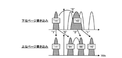
図3は、1個のメモリセルトランジスタMTに2ビットの記憶を行う4値データ記憶方式でのしきい値分布の例を示している。4値データ記憶方式では、上位ページデータ“x”と下位ページデータ“y”で定義される4値データ“xy”の何れか一つをメモリセルトランジスタMTに保持可能である。この、4値データ“xy”は、メモリセルトランジスタMTのしきい値電圧の順に、例えば、データ“11”、“01”、“00”、“10”が割り当てられる。データ“11”は、メモリセルトランジスタMTのしきい値電圧が負の消去状態である。 FIG. 3 shows an example of threshold distribution in a quaternary data storage system in which 2 bits are stored in one memory cell transistor MT. In the quaternary data storage system, any one of the quaternary data “xy” defined by the upper page data “x” and the lower page data “y” can be held in the memory cell transistor MT. For example, data “11”, “01”, “00”, and “10” are assigned to the quaternary data “xy” in order of the threshold voltage of the memory cell transistor MT. Data “11” is an erased state in which the threshold voltage of the memory cell transistor MT is negative.
下位ページ書き込み動作においては、データ“11”(消去状態)のメモリセルトランジスタMTに対して選択的に、下位ビットデータ“y”の書き込みによって、データ“10”が書き込まれる。上位ページ書き込み前のデータ“10”のしきい値分布は、上位ページ書き込み後のデータ“01”とデータ“00”のしきい値分布の中間程度に位置しており、上位ページ書き込み後のしきい値分布よりブロードであってもよい。 In the lower page write operation, data “10” is written to the memory cell transistor MT of data “11” (erased state) selectively by writing lower bit data “y”. The threshold distribution of the data “10” before the upper page write is located in the middle of the threshold distribution of the data “01” and the data “00” after the upper page write. It may be broader than the threshold distribution.
上位ページ書き込み動作においては、データ“11”のメモリセルと、データ“10”のメモリセルに対して、それぞれ選択的に上位ビットデータ“x”の書き込みが行われて、データ“01”およびデータ“00”が書き込まれる。 In the upper page write operation, upper bit data “x” is selectively written into the memory cell of data “11” and the memory cell of data “10”, respectively, and data “01” and data “00” is written.
図4は、メモリセルアレイ10が記憶するデータを説明する図である。図示するように、メモリセルアレイ10は、ファームウェアプログラム11、アドレス変換テーブル12、およびホスト装置200からの書き込みデータであるユーザデータ13を記憶する。ファームウェアプログラム11は、CPU2にSSD100の制御を実行せしめるプログラムであり、アドレス変換テーブル12は、LBAとメモリセルアレイ10の物理アドレスとの対応関係を記述したテーブルである。
FIG. 4 is a diagram for explaining data stored in the
NAND型のメモリセルアレイ10への書き込み方式として、例えば以下に述べる方式が採用される。まず、書き込みの前に、ブロック内の無効データを消去する必要がある。すなわち、消去済みのブロックのうち書き込みがまだ行われていないページに対して順次書き込みが可能であり、既に書き込みが行なわれたページに対する上書きが不可能である。また、上述のように、ホスト装置200から要求される書き込み番地は、ホスト装置200で用いられる論理アドレス(LBA)で指定される。一方、NANDメモリ1へのデータの書き込み番地は、メモリセルアレイ10の物理的な記憶位置(物理アドレス)に基づいて、ページの昇順に書き込みが行なわれる。即ち、物理アドレスは論理アドレスとは無関係に決定される。決定された論理アドレスと物理アドレスとの対応関係は、アドレス変換テーブル12に記録される。そして、データの書き込み要求において指定された論理アドレスが再度指定されて新たなデータの書き込みがホストから要求されると、CPU2は、消去済みのブロックのうちの書き込みがまだ行なわれていないページに対して新たなデータの書き込みを行う。このとき、CPU2は、当該論理アドレスに対応して前回書き込みが行われたページを無効にして、新たなデータの書き込みが行われたページを有効にする。
As a writing method to the NAND type
ここで、メモリセルアレイ10に対する書き込みおよび消去の回数の増加に伴って、フローティングゲート周りの酸化膜が劣化し、その位置に書き込まれたデータが変化しやすくなるという問題がある。また、メモリセルアレイ10に書き込み済みのデータは、プログラムディスターブやリードディスターブにより変化し、データに誤りが生じることがある。一方、ファームウェアプログラム11やアドレス変換テーブル12は、SSD100がホスト装置200の外部記憶装置としての機能を保つために不可欠なデータであり、これらのデータが破壊されると、SSD100の健全性が損なわれる。したがって、これらのデータが訂正不能となるような破壊を防止したり、破壊されてもSSD100が動作するようにこれらのデータを多重化したりすることが望ましい。
Here, as the number of times of writing and erasing with respect to the
そこで、第1の実施形態では、ファームウェアプログラム11およびアドレス変換テーブル12(以降、システムデータ14と総称する)を所定のタイミングで検証し、検証結果がNG(不合格)であった場合にはシステムデータ14をメモリセルアレイ10内の他の位置に移動させるようにした。なお、これらの一連の処理を、信頼性担保処理ということとする。
Therefore, in the first embodiment, the
図5は、信頼性担保処理を実行するためのSSD100の機能構成を説明する図である。図示するように、CPU2は、信頼性担保処理制御部21、コピー先探索部22、データ検証部23、およびデータ操作部24を備えている。信頼性担保処理制御部21は、コピー先探索部22、データ検証部23、およびデータ操作部24を制御する。コピー先探索部22は、システムデータ14の複製先の番地を探索する。データ検証部23は、信頼性担保処理の実行前のシステムデータ14の検証と、複製されたシステムデータ14の検証とを実行する。データ操作部24は、システムデータ14の複製や、複製元のシステムデータ14(即ち信頼性担保処理の実行前のシステムデータ14)の消去などを実行する。なお、これらの機能構成部は、CPU2がファームウェアプログラム11を実行することによって実現される。
FIG. 5 is a diagram illustrating a functional configuration of the
図6は、第1の実施形態のSSD100における信頼性担保処理を説明するフローチャートである。
FIG. 6 is a flowchart for explaining reliability assurance processing in the
まず、信頼性担保処理制御部21は、現時点でシステムデータ14の検証タイミングに至ったか否かを判定する(ステップS1)。現時点がシステムデータ14の検証タイミングではない場合(ステップS1、No)、信頼性担保処理制御部21は、ステップS1の判定処理を再び実行する。なお、検証タイミングはどのようなタイミングに設定するようにしてもよい。例えば、所定の時間間隔で検証が行われるようにしてよいし、電源オフ時や電源オン時を検証タイミングとするようにしてもよい。
First, the reliability guarantee
現時点がシステムデータ14の検証タイミングに達した場合(ステップS1、Yes)、信頼性担保処理制御部21の指令により、データ検証部23は、システムデータ14の検証を実行する(ステップS2)。システムデータ14の検証は、例えば以下のようにして実行される。即ち、データ検証部23は、NANDC5に指令して、システムデータ14をNANDメモリ1からDRAM4に転送せしめる(読み出させる)。ECC回路51は、システムデータ14が転送される際に、第1の誤り訂正符号に基づくエラーの検出および訂正を行い、エラーの訂正を行った場合には、第1の誤り訂正符号によって訂正完了したエラー数をデータ検証部23に報告する。また、訂正不可能なエラーがあった場合、ECC回路51は、データ検証部23にその旨を報告し、データ検証部23は、ECC回路6に指令して、第1の誤り訂正符号により訂正不可能なエラーを第2の誤り訂正符号を用いて訂正せしめる。ECC回路6は、訂正完了したエラー数をデータ検証部23に報告する。
When the current time has reached the verification timing of the system data 14 (step S1, Yes), the
続いて、データ検証部23は、検証結果がNGである(即ちシステムデータ14の信頼性が低下している)か否かを判定する(ステップS3)。ステップS3の判定は、どのようにしておこなわれてもよい。例えば、データ検証部23は、第1の誤り訂正符号による訂正数と第2の誤り訂正符号による訂正数の合計値が所定のしきい値に到達している場合に、システムデータ14の信頼性が低下していると判定し、前記合計値が前記しきい値に到達していない場合に、システムデータ14の信頼性が低下していないと判定することができる。また、データ検証部23は、ステップS2を実行する毎に前記合計値を記録しておき、前記合計値が増加する傾向があるか否かに基づいてシステムデータ14の信頼性が低下しているか否かを判定することができる。即ち、データ検証部23は、前記合計値の現在値および/または過去値を用いて、システムデータ14の信頼性が低下しているか否かを判定することができる。
Subsequently, the
検証結果がOK(合格)であった場合(ステップS3、No)、信頼性担保処理制御部21は、ステップS1の処理を実行する。検証結果がNGであった場合(ステップS3、Yes)、信頼性担保処理制御部21は、ステップS5〜ステップS10のループ処理のためのループインデックスiを0で初期化して(ステップS4)、i=10であるか否かを判定する(ステップS5)。i=10ではない場合(ステップS5、No)、信頼性担保処理制御部21は、コピー先探索部22に指令して、指令を受けたコピー先探索部22は、システムデータ14の複製先の番地を空き領域のうちから選択する(ステップS6)。空き領域のうちのどの番地を選択するかは、ここでは特定の方法に限定されない。例えば、複製先の番地を、空きブロック(即ち有効データを含まないブロック)のうちの1つとしてもよい。
When a verification result is OK (pass) (step S3, No), the reliability ensuring
続いて、信頼性担保処理制御部21は、データ操作部24に指令して、指令をうけたデータ操作部24は、システムデータ14をステップS6にて選択された番地に複製する(ステップS7)。その後、データ検証部23は、信頼性担保処理制御部21からの指令により、ステップS6にて選択された番地に複製されたシステムデータ14(以降、複製データ)の検証を実行し(ステップS8)、検証結果がNGであるか否かを判定する(ステップS9)。なお、ステップS8の処理は、ステップS2の処理と同様であってよい。また、ステップS9の処理は、ステップS2の処理によって得られた第1の誤り訂正符号による訂正数と第2の誤り訂正符号による訂正数との合計値に基づいて行われる。検証結果がNGであった場合(ステップS9、Yes)、信頼性担保処理制御部21は、iを1だけインクリメントし(ステップS10)、ステップS5の処理を実行する。
Subsequently, the reliability guarantee
そして、i=10であった場合には(ステップS5、Yes)、信頼性担保処理制御部21は、データ操作部24に指令して、検証結果が最も良好であった複製データを残し、他の複製データを無効化せしめ(ステップS11)、その後、信頼性担保処理制御部21は、ステップS1の判定処理を実行する。
If i = 10 (step S5, Yes), the reliability guarantee
複製データの検証結果がOK(合格)であった場合(ステップS12、No)、信頼性担保処理制御部21は、データ操作部24に指令して、検証結果がOKとなった複製データを残し、複製元のシステムデータ14を無効化せしめる(ステップS12)。なお、ここで、検証結果がOKとなった複製データのほかにも複製データが存在する場合には、信頼性担保処理制御部21は、データ操作部24に指令して、検証結果がOKとなった複製データを除く複製データを無効化する。信頼性担保処理制御部21は、ステップS12の処理の後、ステップS1の判定処理を実行する。
When the verification result of the duplicate data is OK (pass) (No in step S12), the reliability guarantee
このように、第1の実施形態によれば、データ検証部23は、NANDメモリ1の所定の番地に格納されているシステムデータ14を所定のタイミングでNANDメモリ1から読み出して、前記読み出したシステムデータ14を検証し、コピー先探索部(番地選択部)22は、データ検証部23による検証結果が不合格である場合に、前記NANDメモリ1の複製先の番地を選択し、データ操作部24は、前記選択された複製先の番地に前記システムデータ14を複製する。そして、データ検証部23は、複製データを読み出して、読み出した複製データを検証する。データ操作部24は、複製データの検証結果が合格である場合に、複製元のシステムデータ14を削除する。これにより、SSD100は、システムデータ14の健全性が損なわれる前に当該システムデータ14を他の一定の信頼性が保障された番地に移動させることができるので、システムデータ14が読み出し不可能となるリスクを低減することができる。
Thus, according to the first embodiment, the
また、データ操作部24は、複製データの検証結果が不合格である場合に、複製元のシステムデータ14を消去しないようにしたので、SSD100は、複製元のシステムデータ14がエラー訂正が不可能となる破壊をうけたとしても、複製データをシステムデータ14として使用することができるので、システムデータ14が読み出し不可能となるリスクを低減することができる。
Further, since the
なお、以上の説明においては、データ検証部23は、エラー訂正数に基づいてシステムデータ14または複製データの検証を行うものとして説明したが、エラー検出数に基づいて検証を行うようにしてもよい。
In the above description, the
(第2の実施形態)
第2の実施形態では、SSD100は、システムデータ14の信頼性が低下したとき、システムデータ14を、書き換え回数(即ち消去回数と書き込み回数との合計値)が最も少ないブロックに複製し、システムデータ14を多重化する。
(Second Embodiment)
In the second embodiment, when the reliability of the system data 14 is reduced, the
第2の実施形態のSSD100のハードウェア構成は第1の実施形態と同等であり、個々の機能構成部の動作が異なるだけであるので、以下、第1の実施形態の構成要素を用いて説明する。
Since the hardware configuration of the
図7は、第2の実施形態のSSD100における信頼性担保処理を説明するフローチャートである。まず、第2の実施形態のSSD100においては、ステップS21、ステップS22において、既に説明したステップS1、ステップS2と夫々等しい処理が実行される。そして、データ検証部23は、信頼性担保処理制御部21からの指令に基づいて、システムデータ14の検証結果がNGか否かを判定する(ステップS23)。検証結果がNGであった場合(ステップS23、Yes)、信頼性担保処理制御部21は、コピー先探索部22に指令して、指令を受けたコピー先探索部22は、システムデータ14の複製先として、空きブロックのうちの書き換え回数が最も少ないブロックを選択する(ステップS24)。すると、信頼性担保処理制御部21は、データ操作部24に指令して、指令をうけたデータ操作部24は、システムデータ14をステップS24にて選択されたブロックに複製する(ステップS25)。ステップS25の処理の後、または検証結果がOKであった場合(ステップS23、No)、信頼性担保処理制御部21は、ステップS21の判定処理を実行する。
FIG. 7 is a flowchart for explaining reliability assurance processing in the
このように、第2の実施形態によれば、データ検証部23は、NANDメモリ1の所定のブロックに格納されているシステムデータ14を読み出して、読み出したシステムデータ14を検証し、コピー先探索部22は、検証結果が不合格である場合には、システムデータ14の複製先として、書き換え回数が最小のブロックを選択し、データ操作部24は、システムデータ14を前記選択された書き換え回数が最小のブロックに複製するようにしたので、SSD100は、複製元のシステムデータ14がエラー訂正が不可能となる破壊をうけたとしても、複製データをシステムデータ14として使用することができるので、システムデータ14が読み出し不可能となるリスクを低減することができる。また、第1の実施形態ではSSD100は複製データの検証を行っていたところ、第2の実施形態によればSSD100は複製データの検証を行うことがないので、信頼性担保処理にかかる処理コストを低減することができる。
Thus, according to the second embodiment, the
(第3の実施形態)
なお、第1の実施形態においては、コピー先探索部22は、任意の方法に基づいてシステムデータ14の複製先の番地を選択するとして説明したが、コピー先探索部22は、第2の実施形態と同様に、空きブロックのうちの書き換え回数が最も少ないブロックを複製先の番地として選択するようにしてもよい。このようにすることによって、出来るだけ健全性が高い番地にシステムデータ14を複製することができるようになるので、一回の信頼性担保処理におけるステップS5〜ステップS10のループ処理の実行回数を低減せしめることができるようになる。
(Third embodiment)
In the first embodiment, the copy
また、第1の実施形態および第2の実施形態においては、コピー先探索部22は、空いている領域から複製先の番地を探索するものとして説明したが、コピー先探索部22は、有効データが途中のページまで書き込まれたブロックの、有効データに後続するページを複製先の番地として選択することもできる。
In the first embodiment and the second embodiment, the copy
また、第2の実施形態においては、コピー先探索部22は、空きブロックのうちの書き換え回数が最もすくないブロックをシステムデータ14の複製先のブロックに選択するとして説明したが、全ブロックのうちの書き換え回数が最も少ないブロックが有効データを含むブロックである場合には、当該ブロックに書き込まれている有効データを他の空きブロックに移動した上で、空きブロックとなった前記ブロックをシステムデータ14の複製先として選択するようにしてもよい。
Further, in the second embodiment, the copy
また、第1の実施形態においては、データ操作部24は、ステップS5〜ステップS10のループ処理を10回実施しても複製データの検査結果がOKとならない場合には、システムデータ14を多重化するものとして説明したが、SLCモードで書き込まれたデータはMLCモードで書き込まれたデータよりも失われにくいことを利用して、信頼性担保処理制御部21は、以下のように制御を実行するようにしてもよい。即ち、初期状態においては、システムデータ14は、MLCモードで書き込まれており、ステップS5〜ステップS10のループ処理を10回実施しても複製データの検査結果がOKとならない場合には、信頼性担保処理制御部21は、データ操作部24に指令して、指令をうけたデータ操作部24は、SLCモードでシステムデータ14を複製するようにしてもよい。なお、SLCモードでシステムデータ14を複製した場合には、信頼性担保処理制御部21は、データ操作部24に、元のシステムデータ14を消去せしめるようにしてもよいし、元のシステムデータ14を残しておくようにしてもよい。
In the first embodiment, the
本発明のいくつかの実施形態を説明したが、これらの実施形態は、例として提示したものであり、発明の範囲を限定することは意図していない。これら新規な実施形態は、その他の様々な形態で実施されることが可能であり、発明の要旨を逸脱しない範囲で、種々の省略、置き換え、変更を行うことができる。これら実施形態やその変形は、発明の範囲や要旨に含まれるとともに、特許請求の範囲に記載された発明とその均等の範囲に含まれる。 Although several embodiments of the present invention have been described, these embodiments are presented by way of example and are not intended to limit the scope of the invention. These novel embodiments can be implemented in various other forms, and various omissions, replacements, and changes can be made without departing from the scope of the invention. These embodiments and modifications thereof are included in the scope and gist of the invention, and are included in the invention described in the claims and the equivalents thereof.
1 NANDメモリ、2 CPU、3 ホストI/F、4 DRAM、5 NANDC、6 ECC回路、10 メモリセルアレイ、11 ファームウェアプログラム、12 アドレス変換テーブル、13 ユーザデータ、14 システムデータ、21 信頼性担保処理制御部、22 コピー先探索部、23 データ検証部、24 データ操作部、200 ホスト装置。 1 NAND memory, 2 CPU, 3 Host I / F, 4 DRAM, 5 NANDC, 6 ECC circuit, 10 Memory cell array, 11 Firmware program, 12 Address conversion table, 13 User data, 14 System data, 21 Reliability control processing control Unit, 22 copy destination search unit, 23 data verification unit, 24 data operation unit, 200 host device.
Claims (8)
所定のタイミングで前記第1の番地からシステムデータを読み出して、前記第1の番地から読み出したシステムデータを検証する第1のデータ検証部と、
前記第1のデータ検証部による検証結果が不合格である場合に、前記不揮発性メモリにおける、前記第1の番地と異なる第2の番地を選択する番地選択部と、
前記番地選択部が選択した前記第2の番地に前記第1の番地に記憶されているシステムデータを複製する第1のデータ操作部と、
前記第2の番地に複製されたシステムデータを読み出して、前記第2の番地から読み出したシステムデータを検証する第2のデータ検証部と、
前記第2のデータ検証部による検証結果が合格である場合に、前記第1の番地に記憶されているシステムデータを消去する第2のデータ操作部と、
を備えることを特徴とするメモリシステム。 A non-volatile memory for storing system data at a first address;
A first data verification unit that reads system data from the first address at a predetermined timing and verifies the system data read from the first address;
An address selection unit that selects a second address different from the first address in the nonvolatile memory when the verification result by the first data verification unit is unacceptable;
A first data operation unit that replicates system data stored in the first address to the second address selected by the address selection unit;
A second data verification unit that reads the system data copied to the second address and verifies the system data read from the second address;
A second data operation unit for erasing system data stored in the first address when the verification result by the second data verification unit is acceptable;
A memory system comprising:
ことを特徴とする請求項1に記載のメモリシステム。 The second data operation unit does not erase the system data stored in the first address when the verification result by the first data verification unit fails.
The memory system according to claim 1.
ことを特徴とする請求項1または請求項2に記載のメモリシステム。 The first data verification unit and the second data verification unit perform error detection or error correction on the system data read from the first or second address to obtain an error detection number or error correction number. Verifying system data read from the first or second address based on,
The memory system according to claim 1, wherein the memory system is a memory system.
ことを特徴とする請求項3に記載のメモリシステム。 The address selection unit selects, as the second address, a block having the smallest number of rewrites in the nonvolatile memory.
The memory system according to claim 3.
ことを特徴とする請求項1に記載のメモリシステム。 The address selection unit sets the second address for each verification until the verification result by the second data verification unit passes or the number of verifications by the second data verification unit reaches a predetermined number. Select a new one
The memory system according to claim 1.
ことを特徴とする請求項5に記載のメモリシステム。 The system data stored at the first address is stored in the MLC mode, and when the number of verifications reaches a predetermined number, the second data verification unit is stored at the first address. Replicating system data in SLC mode to any of the selected second addresses,
The memory system according to claim 5.
所定のタイミングで前記第1のブロックからシステムデータを読み出して、前記第1のブロックから読み出したシステムデータを検証するデータ検証部と、
前記データ検証部による検証結果が不合格である場合に、前記不揮発性メモリのうちの書き換え回数が最小の第2のブロックを選択する番地選択部と、
前記第2のブロックに前記第1のブロックに記憶されているシステムデータを複製するデータ操作部と、
を備えることを特徴とするメモリシステム。 A non-volatile memory for storing system data in the first block;
A data verification unit that reads system data from the first block at a predetermined timing and verifies the system data read from the first block;
When the verification result by the data verification unit is unacceptable, an address selection unit that selects the second block with the smallest number of rewrites in the nonvolatile memory;
A data operation unit for copying the system data stored in the first block to the second block;
A memory system comprising:
ことを特徴とする請求項7に記載のメモリシステム。 The data verification unit performs error detection or error correction on the system data read from the first block, and verifies the system data read from the first block based on the number of error detection or error correction To
The memory system according to claim 7.
Priority Applications (2)
| Application Number | Priority Date | Filing Date | Title |
|---|---|---|---|
| JP2012066734A JP2013196673A (en) | 2012-03-23 | 2012-03-23 | Memory system |
| US13/768,344 US20130254463A1 (en) | 2012-03-23 | 2013-02-15 | Memory system |
Applications Claiming Priority (1)
| Application Number | Priority Date | Filing Date | Title |
|---|---|---|---|
| JP2012066734A JP2013196673A (en) | 2012-03-23 | 2012-03-23 | Memory system |
Publications (1)
| Publication Number | Publication Date |
|---|---|
| JP2013196673A true JP2013196673A (en) | 2013-09-30 |
Family
ID=49395459
Family Applications (1)
| Application Number | Title | Priority Date | Filing Date |
|---|---|---|---|
| JP2012066734A Pending JP2013196673A (en) | 2012-03-23 | 2012-03-23 | Memory system |
Country Status (1)
| Country | Link |
|---|---|
| JP (1) | JP2013196673A (en) |
Cited By (2)
| Publication number | Priority date | Publication date | Assignee | Title |
|---|---|---|---|---|
| CN107066394A (en) * | 2017-03-31 | 2017-08-18 | 深圳市金印达科技有限公司 | The data read-write method and system of a kind of imaging device |
| CN110119360A (en) * | 2018-02-06 | 2019-08-13 | 爱思开海力士有限公司 | Storage device and its operating method |
Citations (8)
| Publication number | Priority date | Publication date | Assignee | Title |
|---|---|---|---|---|
| US9031A (en) * | 1852-06-15 | Improvement in harvesters | ||
| JP2004234052A (en) * | 2003-01-28 | 2004-08-19 | Renesas Technology Corp | Storage device |
| WO2006046425A1 (en) * | 2004-10-29 | 2006-05-04 | Matsushita Electric Industrial Co., Ltd. | Nonvolatile storage device and nonvolatile storage system |
| JP2007310916A (en) * | 2007-09-03 | 2007-11-29 | Renesas Technology Corp | Memory card |
| JP2008021333A (en) * | 2007-09-28 | 2008-01-31 | Renesas Technology Corp | Non-volatile memory system |
| WO2009090731A1 (en) * | 2008-01-16 | 2009-07-23 | Fujitsu Limited | Semiconductor storage device, controlling apparatus and controlling method |
| JP2010015477A (en) * | 2008-07-07 | 2010-01-21 | Nec Electronics Corp | Flash memory control device and flash memory control method |
| JP2011059907A (en) * | 2009-09-09 | 2011-03-24 | Nec Corp | Terminal device, method of managing nonvolatile memory used therein, and program therefor |
-
2012
- 2012-03-23 JP JP2012066734A patent/JP2013196673A/en active Pending
Patent Citations (8)
| Publication number | Priority date | Publication date | Assignee | Title |
|---|---|---|---|---|
| US9031A (en) * | 1852-06-15 | Improvement in harvesters | ||
| JP2004234052A (en) * | 2003-01-28 | 2004-08-19 | Renesas Technology Corp | Storage device |
| WO2006046425A1 (en) * | 2004-10-29 | 2006-05-04 | Matsushita Electric Industrial Co., Ltd. | Nonvolatile storage device and nonvolatile storage system |
| JP2007310916A (en) * | 2007-09-03 | 2007-11-29 | Renesas Technology Corp | Memory card |
| JP2008021333A (en) * | 2007-09-28 | 2008-01-31 | Renesas Technology Corp | Non-volatile memory system |
| WO2009090731A1 (en) * | 2008-01-16 | 2009-07-23 | Fujitsu Limited | Semiconductor storage device, controlling apparatus and controlling method |
| JP2010015477A (en) * | 2008-07-07 | 2010-01-21 | Nec Electronics Corp | Flash memory control device and flash memory control method |
| JP2011059907A (en) * | 2009-09-09 | 2011-03-24 | Nec Corp | Terminal device, method of managing nonvolatile memory used therein, and program therefor |
Cited By (2)
| Publication number | Priority date | Publication date | Assignee | Title |
|---|---|---|---|---|
| CN107066394A (en) * | 2017-03-31 | 2017-08-18 | 深圳市金印达科技有限公司 | The data read-write method and system of a kind of imaging device |
| CN110119360A (en) * | 2018-02-06 | 2019-08-13 | 爱思开海力士有限公司 | Storage device and its operating method |
Similar Documents
| Publication | Publication Date | Title |
|---|---|---|
| US10324789B2 (en) | Flash memory controller and memory device for accessing flash memory module, and associated method | |
| US9298545B2 (en) | Data protection across multiple memory blocks | |
| KR101903915B1 (en) | Partial bad block detection and re-use using epwr for block based architectures | |
| US20130254463A1 (en) | Memory system | |
| US10915394B1 (en) | Schemes for protecting data in NVM device using small storage footprint | |
| KR20120055725A (en) | Stripe-based memory operation | |
| JP2013089082A (en) | Memory controller, semiconductor storage system and memory control method | |
| US20210264980A1 (en) | Identifying failure type in NVM programmed in SLC mode using a single programming pulse with no verification | |
| US20160077913A1 (en) | Method of controlling nonvolatile memory | |
| US11467903B2 (en) | Memory system and operating method thereof | |
| JP2013196673A (en) | Memory system | |
| US20220083255A1 (en) | Memory system and operating method thereof | |
| US20170373705A1 (en) | Apparatuses and methods for erasure-assisted ecc decoding | |
| US20230039982A1 (en) | Memory system and operating method of memory system | |
| US20240054046A1 (en) | Error-handling management during copyback operations in memory devices | |
| TWI823649B (en) | Control method of flash memory controller, flash memory controller, and electronic device | |
| CN113961141B (en) | Memory system, memory controller, and method of operating memory system | |
| TWI691967B (en) | Decoding method and associated flash memory controller and electronic device | |
| US20230387941A1 (en) | Controller and operating method thereof for determining reliability data based on syndrome weight | |
| US11544003B2 (en) | Memory system, memory controller, and method of operating memory system | |
| US11636007B2 (en) | Memory system and operating method thereof for flushing data in data cache with parity | |
| US11050442B2 (en) | Reducing the latency of a syndrome-based quasi-cyclic decoder | |
| TWI575530B (en) | Method for accessing flash memory module and associated flash memory controller and memory device | |
| JP5710815B1 (en) | Semiconductor memory device | |
| TW202328927A (en) | Method for performing access control of memory device with aid of aggressor bit information, memory device, and controller of memory device |
Legal Events
| Date | Code | Title | Description |
|---|---|---|---|
| A621 | Written request for application examination |
Free format text: JAPANESE INTERMEDIATE CODE: A621 Effective date: 20140210 |
|
| A977 | Report on retrieval |
Free format text: JAPANESE INTERMEDIATE CODE: A971007 Effective date: 20140613 |
|
| A131 | Notification of reasons for refusal |
Free format text: JAPANESE INTERMEDIATE CODE: A131 Effective date: 20140617 |
|
| A02 | Decision of refusal |
Free format text: JAPANESE INTERMEDIATE CODE: A02 Effective date: 20141021 |