JP2012517610A - Micro relief structure - Google Patents
Micro relief structure Download PDFInfo
- Publication number
- JP2012517610A JP2012517610A JP2011548722A JP2011548722A JP2012517610A JP 2012517610 A JP2012517610 A JP 2012517610A JP 2011548722 A JP2011548722 A JP 2011548722A JP 2011548722 A JP2011548722 A JP 2011548722A JP 2012517610 A JP2012517610 A JP 2012517610A
- Authority
- JP
- Japan
- Prior art keywords
- layer
- hierarchical structure
- relief pattern
- fixed
- fixed layer
- Prior art date
- Legal status (The legal status is an assumption and is not a legal conclusion. Google has not performed a legal analysis and makes no representation as to the accuracy of the status listed.)
- Pending
Links
- 238000000034 method Methods 0.000 claims abstract description 62
- 239000000758 substrate Substances 0.000 claims abstract description 45
- 238000012545 processing Methods 0.000 claims abstract description 20
- 230000001681 protective effect Effects 0.000 claims abstract description 9
- 229910052751 metal Inorganic materials 0.000 claims description 28
- 239000002184 metal Substances 0.000 claims description 25
- 239000000463 material Substances 0.000 claims description 18
- 230000003287 optical effect Effects 0.000 claims description 11
- 230000015572 biosynthetic process Effects 0.000 claims description 9
- 239000012815 thermoplastic material Substances 0.000 claims description 8
- 238000000151 deposition Methods 0.000 claims description 7
- 229910010272 inorganic material Inorganic materials 0.000 claims description 4
- 239000011147 inorganic material Substances 0.000 claims description 4
- 239000011368 organic material Substances 0.000 claims description 4
- 239000010410 layer Substances 0.000 description 58
- 239000010408 film Substances 0.000 description 22
- 238000003475 lamination Methods 0.000 description 12
- 229920001169 thermoplastic Polymers 0.000 description 12
- 239000004416 thermosoftening plastic Substances 0.000 description 12
- 239000012528 membrane Substances 0.000 description 5
- 239000011241 protective layer Substances 0.000 description 5
- 230000008021 deposition Effects 0.000 description 4
- 238000004049 embossing Methods 0.000 description 4
- 238000004519 manufacturing process Methods 0.000 description 4
- 230000000873 masking effect Effects 0.000 description 3
- 239000010409 thin film Substances 0.000 description 3
- 239000003989 dielectric material Substances 0.000 description 2
- 230000000694 effects Effects 0.000 description 2
- 238000011835 investigation Methods 0.000 description 2
- 230000008018 melting Effects 0.000 description 2
- 238000002844 melting Methods 0.000 description 2
- 238000000059 patterning Methods 0.000 description 2
- 238000007639 printing Methods 0.000 description 2
- 230000005855 radiation Effects 0.000 description 2
- 238000004873 anchoring Methods 0.000 description 1
- 230000009286 beneficial effect Effects 0.000 description 1
- 239000011248 coating agent Substances 0.000 description 1
- 238000000576 coating method Methods 0.000 description 1
- 230000006378 damage Effects 0.000 description 1
- 238000000354 decomposition reaction Methods 0.000 description 1
- 238000005034 decoration Methods 0.000 description 1
- 238000001514 detection method Methods 0.000 description 1
- 238000011161 development Methods 0.000 description 1
- 238000010586 diagram Methods 0.000 description 1
- 238000010017 direct printing Methods 0.000 description 1
- 238000009826 distribution Methods 0.000 description 1
- 238000003487 electrochemical reaction Methods 0.000 description 1
- 230000005670 electromagnetic radiation Effects 0.000 description 1
- 238000010894 electron beam technology Methods 0.000 description 1
- 239000011810 insulating material Substances 0.000 description 1
- 230000002427 irreversible effect Effects 0.000 description 1
- 238000001459 lithography Methods 0.000 description 1
- 238000012423 maintenance Methods 0.000 description 1
- 239000007769 metal material Substances 0.000 description 1
- 238000001465 metallisation Methods 0.000 description 1
- 239000002105 nanoparticle Substances 0.000 description 1
- 229910052755 nonmetal Inorganic materials 0.000 description 1
- 230000000704 physical effect Effects 0.000 description 1
- 229920000515 polycarbonate Polymers 0.000 description 1
- 239000004417 polycarbonate Substances 0.000 description 1
- 229920005989 resin Polymers 0.000 description 1
- 239000011347 resin Substances 0.000 description 1
- 239000004065 semiconductor Substances 0.000 description 1
- 239000002210 silicon-based material Substances 0.000 description 1
- 239000007787 solid Substances 0.000 description 1
- 229920005992 thermoplastic resin Polymers 0.000 description 1
- 238000003325 tomography Methods 0.000 description 1
- 230000000007 visual effect Effects 0.000 description 1
Images


Classifications
-
- B—PERFORMING OPERATIONS; TRANSPORTING
- B32—LAYERED PRODUCTS
- B32B—LAYERED PRODUCTS, i.e. PRODUCTS BUILT-UP OF STRATA OF FLAT OR NON-FLAT, e.g. CELLULAR OR HONEYCOMB, FORM
- B32B3/00—Layered products comprising a layer with external or internal discontinuities or unevennesses, or a layer of non-planar shape; Layered products comprising a layer having particular features of form
- B32B3/26—Layered products comprising a layer with external or internal discontinuities or unevennesses, or a layer of non-planar shape; Layered products comprising a layer having particular features of form characterised by a particular shape of the outline of the cross-section of a continuous layer; characterised by a layer with cavities or internal voids ; characterised by an apertured layer
- B32B3/30—Layered products comprising a layer with external or internal discontinuities or unevennesses, or a layer of non-planar shape; Layered products comprising a layer having particular features of form characterised by a particular shape of the outline of the cross-section of a continuous layer; characterised by a layer with cavities or internal voids ; characterised by an apertured layer characterised by a layer formed with recesses or projections, e.g. hollows, grooves, protuberances, ribs
-
- B—PERFORMING OPERATIONS; TRANSPORTING
- B42—BOOKBINDING; ALBUMS; FILES; SPECIAL PRINTED MATTER
- B42D—BOOKS; BOOK COVERS; LOOSE LEAVES; PRINTED MATTER CHARACTERISED BY IDENTIFICATION OR SECURITY FEATURES; PRINTED MATTER OF SPECIAL FORMAT OR STYLE NOT OTHERWISE PROVIDED FOR; DEVICES FOR USE THEREWITH AND NOT OTHERWISE PROVIDED FOR; MOVABLE-STRIP WRITING OR READING APPARATUS
- B42D25/00—Information-bearing cards or sheet-like structures characterised by identification or security features; Manufacture thereof
- B42D25/30—Identification or security features, e.g. for preventing forgery
- B42D25/324—Reliefs
-
- B—PERFORMING OPERATIONS; TRANSPORTING
- B05—SPRAYING OR ATOMISING IN GENERAL; APPLYING FLUENT MATERIALS TO SURFACES, IN GENERAL
- B05D—PROCESSES FOR APPLYING FLUENT MATERIALS TO SURFACES, IN GENERAL
- B05D5/00—Processes for applying liquids or other fluent materials to surfaces to obtain special surface effects, finishes or structures
- B05D5/06—Processes for applying liquids or other fluent materials to surfaces to obtain special surface effects, finishes or structures to obtain multicolour or other optical effects
-
- B—PERFORMING OPERATIONS; TRANSPORTING
- B32—LAYERED PRODUCTS
- B32B—LAYERED PRODUCTS, i.e. PRODUCTS BUILT-UP OF STRATA OF FLAT OR NON-FLAT, e.g. CELLULAR OR HONEYCOMB, FORM
- B32B27/00—Layered products comprising a layer of synthetic resin
- B32B27/06—Layered products comprising a layer of synthetic resin as the main or only constituent of a layer, which is next to another layer of the same or of a different material
- B32B27/08—Layered products comprising a layer of synthetic resin as the main or only constituent of a layer, which is next to another layer of the same or of a different material of synthetic resin
-
- B—PERFORMING OPERATIONS; TRANSPORTING
- B32—LAYERED PRODUCTS
- B32B—LAYERED PRODUCTS, i.e. PRODUCTS BUILT-UP OF STRATA OF FLAT OR NON-FLAT, e.g. CELLULAR OR HONEYCOMB, FORM
- B32B27/00—Layered products comprising a layer of synthetic resin
- B32B27/36—Layered products comprising a layer of synthetic resin comprising polyesters
-
- B—PERFORMING OPERATIONS; TRANSPORTING
- B32—LAYERED PRODUCTS
- B32B—LAYERED PRODUCTS, i.e. PRODUCTS BUILT-UP OF STRATA OF FLAT OR NON-FLAT, e.g. CELLULAR OR HONEYCOMB, FORM
- B32B3/00—Layered products comprising a layer with external or internal discontinuities or unevennesses, or a layer of non-planar shape; Layered products comprising a layer having particular features of form
- B32B3/02—Layered products comprising a layer with external or internal discontinuities or unevennesses, or a layer of non-planar shape; Layered products comprising a layer having particular features of form characterised by features of form at particular places, e.g. in edge regions
- B32B3/08—Layered products comprising a layer with external or internal discontinuities or unevennesses, or a layer of non-planar shape; Layered products comprising a layer having particular features of form characterised by features of form at particular places, e.g. in edge regions characterised by added members at particular parts
-
- B—PERFORMING OPERATIONS; TRANSPORTING
- B32—LAYERED PRODUCTS
- B32B—LAYERED PRODUCTS, i.e. PRODUCTS BUILT-UP OF STRATA OF FLAT OR NON-FLAT, e.g. CELLULAR OR HONEYCOMB, FORM
- B32B7/00—Layered products characterised by the relation between layers; Layered products characterised by the relative orientation of features between layers, or by the relative values of a measurable parameter between layers, i.e. products comprising layers having different physical, chemical or physicochemical properties; Layered products characterised by the interconnection of layers
- B32B7/04—Interconnection of layers
- B32B7/12—Interconnection of layers using interposed adhesives or interposed materials with bonding properties
-
- B—PERFORMING OPERATIONS; TRANSPORTING
- B42—BOOKBINDING; ALBUMS; FILES; SPECIAL PRINTED MATTER
- B42D—BOOKS; BOOK COVERS; LOOSE LEAVES; PRINTED MATTER CHARACTERISED BY IDENTIFICATION OR SECURITY FEATURES; PRINTED MATTER OF SPECIAL FORMAT OR STYLE NOT OTHERWISE PROVIDED FOR; DEVICES FOR USE THEREWITH AND NOT OTHERWISE PROVIDED FOR; MOVABLE-STRIP WRITING OR READING APPARATUS
- B42D15/00—Printed matter of special format or style not otherwise provided for
-
- B—PERFORMING OPERATIONS; TRANSPORTING
- B42—BOOKBINDING; ALBUMS; FILES; SPECIAL PRINTED MATTER
- B42D—BOOKS; BOOK COVERS; LOOSE LEAVES; PRINTED MATTER CHARACTERISED BY IDENTIFICATION OR SECURITY FEATURES; PRINTED MATTER OF SPECIAL FORMAT OR STYLE NOT OTHERWISE PROVIDED FOR; DEVICES FOR USE THEREWITH AND NOT OTHERWISE PROVIDED FOR; MOVABLE-STRIP WRITING OR READING APPARATUS
- B42D25/00—Information-bearing cards or sheet-like structures characterised by identification or security features; Manufacture thereof
- B42D25/30—Identification or security features, e.g. for preventing forgery
- B42D25/328—Diffraction gratings; Holograms
-
- B—PERFORMING OPERATIONS; TRANSPORTING
- B42—BOOKBINDING; ALBUMS; FILES; SPECIAL PRINTED MATTER
- B42D—BOOKS; BOOK COVERS; LOOSE LEAVES; PRINTED MATTER CHARACTERISED BY IDENTIFICATION OR SECURITY FEATURES; PRINTED MATTER OF SPECIAL FORMAT OR STYLE NOT OTHERWISE PROVIDED FOR; DEVICES FOR USE THEREWITH AND NOT OTHERWISE PROVIDED FOR; MOVABLE-STRIP WRITING OR READING APPARATUS
- B42D25/00—Information-bearing cards or sheet-like structures characterised by identification or security features; Manufacture thereof
- B42D25/40—Manufacture
- B42D25/405—Marking
- B42D25/43—Marking by removal of material
- B42D25/435—Marking by removal of material using electromagnetic radiation, e.g. laser
-
- B—PERFORMING OPERATIONS; TRANSPORTING
- B42—BOOKBINDING; ALBUMS; FILES; SPECIAL PRINTED MATTER
- B42D—BOOKS; BOOK COVERS; LOOSE LEAVES; PRINTED MATTER CHARACTERISED BY IDENTIFICATION OR SECURITY FEATURES; PRINTED MATTER OF SPECIAL FORMAT OR STYLE NOT OTHERWISE PROVIDED FOR; DEVICES FOR USE THEREWITH AND NOT OTHERWISE PROVIDED FOR; MOVABLE-STRIP WRITING OR READING APPARATUS
- B42D25/00—Information-bearing cards or sheet-like structures characterised by identification or security features; Manufacture thereof
- B42D25/40—Manufacture
- B42D25/45—Associating two or more layers
-
- G—PHYSICS
- G02—OPTICS
- G02B—OPTICAL ELEMENTS, SYSTEMS OR APPARATUS
- G02B5/00—Optical elements other than lenses
- G02B5/18—Diffraction gratings
-
- G—PHYSICS
- G02—OPTICS
- G02B—OPTICAL ELEMENTS, SYSTEMS OR APPARATUS
- G02B5/00—Optical elements other than lenses
- G02B5/32—Holograms used as optical elements
-
- H—ELECTRICITY
- H05—ELECTRIC TECHNIQUES NOT OTHERWISE PROVIDED FOR
- H05K—PRINTED CIRCUITS; CASINGS OR CONSTRUCTIONAL DETAILS OF ELECTRIC APPARATUS; MANUFACTURE OF ASSEMBLAGES OF ELECTRICAL COMPONENTS
- H05K3/00—Apparatus or processes for manufacturing printed circuits
-
- B—PERFORMING OPERATIONS; TRANSPORTING
- B32—LAYERED PRODUCTS
- B32B—LAYERED PRODUCTS, i.e. PRODUCTS BUILT-UP OF STRATA OF FLAT OR NON-FLAT, e.g. CELLULAR OR HONEYCOMB, FORM
- B32B2255/00—Coating on the layer surface
- B32B2255/10—Coating on the layer surface on synthetic resin layer or on natural or synthetic rubber layer
-
- B—PERFORMING OPERATIONS; TRANSPORTING
- B32—LAYERED PRODUCTS
- B32B—LAYERED PRODUCTS, i.e. PRODUCTS BUILT-UP OF STRATA OF FLAT OR NON-FLAT, e.g. CELLULAR OR HONEYCOMB, FORM
- B32B2255/00—Coating on the layer surface
- B32B2255/20—Inorganic coating
- B32B2255/205—Metallic coating
-
- B—PERFORMING OPERATIONS; TRANSPORTING
- B32—LAYERED PRODUCTS
- B32B—LAYERED PRODUCTS, i.e. PRODUCTS BUILT-UP OF STRATA OF FLAT OR NON-FLAT, e.g. CELLULAR OR HONEYCOMB, FORM
- B32B2307/00—Properties of the layers or laminate
- B32B2307/20—Properties of the layers or laminate having particular electrical or magnetic properties, e.g. piezoelectric
- B32B2307/206—Insulating
-
- B—PERFORMING OPERATIONS; TRANSPORTING
- B32—LAYERED PRODUCTS
- B32B—LAYERED PRODUCTS, i.e. PRODUCTS BUILT-UP OF STRATA OF FLAT OR NON-FLAT, e.g. CELLULAR OR HONEYCOMB, FORM
- B32B2307/00—Properties of the layers or laminate
- B32B2307/40—Properties of the layers or laminate having particular optical properties
-
- B—PERFORMING OPERATIONS; TRANSPORTING
- B32—LAYERED PRODUCTS
- B32B—LAYERED PRODUCTS, i.e. PRODUCTS BUILT-UP OF STRATA OF FLAT OR NON-FLAT, e.g. CELLULAR OR HONEYCOMB, FORM
- B32B2307/00—Properties of the layers or laminate
- B32B2307/50—Properties of the layers or laminate having particular mechanical properties
-
- B—PERFORMING OPERATIONS; TRANSPORTING
- B32—LAYERED PRODUCTS
- B32B—LAYERED PRODUCTS, i.e. PRODUCTS BUILT-UP OF STRATA OF FLAT OR NON-FLAT, e.g. CELLULAR OR HONEYCOMB, FORM
- B32B2307/00—Properties of the layers or laminate
- B32B2307/70—Other properties
- B32B2307/75—Printability
-
- B—PERFORMING OPERATIONS; TRANSPORTING
- B32—LAYERED PRODUCTS
- B32B—LAYERED PRODUCTS, i.e. PRODUCTS BUILT-UP OF STRATA OF FLAT OR NON-FLAT, e.g. CELLULAR OR HONEYCOMB, FORM
- B32B2425/00—Cards, e.g. identity cards, credit cards
-
- B42D2033/10—
-
- B42D2033/30—
-
- B42D2033/46—
-
- B—PERFORMING OPERATIONS; TRANSPORTING
- B42—BOOKBINDING; ALBUMS; FILES; SPECIAL PRINTED MATTER
- B42D—BOOKS; BOOK COVERS; LOOSE LEAVES; PRINTED MATTER CHARACTERISED BY IDENTIFICATION OR SECURITY FEATURES; PRINTED MATTER OF SPECIAL FORMAT OR STYLE NOT OTHERWISE PROVIDED FOR; DEVICES FOR USE THEREWITH AND NOT OTHERWISE PROVIDED FOR; MOVABLE-STRIP WRITING OR READING APPARATUS
- B42D25/00—Information-bearing cards or sheet-like structures characterised by identification or security features; Manufacture thereof
- B42D25/20—Information-bearing cards or sheet-like structures characterised by identification or security features; Manufacture thereof characterised by a particular use or purpose
- B42D25/23—Identity cards
-
- B—PERFORMING OPERATIONS; TRANSPORTING
- B42—BOOKBINDING; ALBUMS; FILES; SPECIAL PRINTED MATTER
- B42D—BOOKS; BOOK COVERS; LOOSE LEAVES; PRINTED MATTER CHARACTERISED BY IDENTIFICATION OR SECURITY FEATURES; PRINTED MATTER OF SPECIAL FORMAT OR STYLE NOT OTHERWISE PROVIDED FOR; DEVICES FOR USE THEREWITH AND NOT OTHERWISE PROVIDED FOR; MOVABLE-STRIP WRITING OR READING APPARATUS
- B42D25/00—Information-bearing cards or sheet-like structures characterised by identification or security features; Manufacture thereof
- B42D25/40—Manufacture
- B42D25/45—Associating two or more layers
- B42D25/46—Associating two or more layers using pressure
-
- Y—GENERAL TAGGING OF NEW TECHNOLOGICAL DEVELOPMENTS; GENERAL TAGGING OF CROSS-SECTIONAL TECHNOLOGIES SPANNING OVER SEVERAL SECTIONS OF THE IPC; TECHNICAL SUBJECTS COVERED BY FORMER USPC CROSS-REFERENCE ART COLLECTIONS [XRACs] AND DIGESTS
- Y10—TECHNICAL SUBJECTS COVERED BY FORMER USPC
- Y10T—TECHNICAL SUBJECTS COVERED BY FORMER US CLASSIFICATION
- Y10T428/00—Stock material or miscellaneous articles
- Y10T428/24—Structurally defined web or sheet [e.g., overall dimension, etc.]
- Y10T428/24479—Structurally defined web or sheet [e.g., overall dimension, etc.] including variation in thickness
- Y10T428/24521—Structurally defined web or sheet [e.g., overall dimension, etc.] including variation in thickness with component conforming to contour of nonplanar surface
-
- Y—GENERAL TAGGING OF NEW TECHNOLOGICAL DEVELOPMENTS; GENERAL TAGGING OF CROSS-SECTIONAL TECHNOLOGIES SPANNING OVER SEVERAL SECTIONS OF THE IPC; TECHNICAL SUBJECTS COVERED BY FORMER USPC CROSS-REFERENCE ART COLLECTIONS [XRACs] AND DIGESTS
- Y10—TECHNICAL SUBJECTS COVERED BY FORMER USPC
- Y10T—TECHNICAL SUBJECTS COVERED BY FORMER US CLASSIFICATION
- Y10T428/00—Stock material or miscellaneous articles
- Y10T428/24—Structurally defined web or sheet [e.g., overall dimension, etc.]
- Y10T428/24479—Structurally defined web or sheet [e.g., overall dimension, etc.] including variation in thickness
- Y10T428/24612—Composite web or sheet
Landscapes
- Engineering & Computer Science (AREA)
- Manufacturing & Machinery (AREA)
- Physics & Mathematics (AREA)
- Optics & Photonics (AREA)
- Microelectronics & Electronic Packaging (AREA)
- General Physics & Mathematics (AREA)
- Electromagnetism (AREA)
- General Health & Medical Sciences (AREA)
- Toxicology (AREA)
- Health & Medical Sciences (AREA)
- Holo Graphy (AREA)
- Diffracting Gratings Or Hologram Optical Elements (AREA)
- Credit Cards Or The Like (AREA)
- Shaping Of Tube Ends By Bending Or Straightening (AREA)
- Laminated Bodies (AREA)
Abstract
本発明は、階層構造における層の表面上にレリーフパターンを形成し、次に、上記階層構造の後続処理の際に下層のレリーフパターンの保護する保護固定層を上記レリーフパターンの少なくとも一部に形成する、階層構造の一部としてレリーフパターンを形成する方法を提供する。その結果、上記レリーフの少なくとも一部には、例えばレリーフパターンが設けられる積層構造を形成する場合などの上記階層構造の後続処理の際にレリーフパターンの特性を保持する保護固定層が設けられている、基材の表面上に形成されたレリーフパターンを有する基材を含む階層構造を提供する。 The present invention forms a relief pattern on the surface of the layer in the hierarchical structure, and then forms a protective fixing layer that protects the underlying relief pattern on at least a part of the relief pattern during subsequent processing of the hierarchical structure. A method for forming a relief pattern as part of a hierarchical structure is provided. As a result, at least a part of the relief is provided with a protective fixing layer that retains the characteristics of the relief pattern during subsequent processing of the hierarchical structure, such as when forming a laminated structure provided with a relief pattern. Providing a hierarchical structure comprising a substrate having a relief pattern formed on the surface of the substrate.
Description
本発明は、マイクロレリーフ構造、埋め込み型薄膜構造を採用する構造、及びそれら製造方法に関する。 The present invention relates to a microrelief structure, a structure that employs an embedded thin film structure, and a method for manufacturing the structure.
種々の材料内にマイクロサイズやナノサイズのレリーフをエンボス加工する多くの技法が存在する。しかしながら、特に熱可塑性材料を用いた際に、例えば比較的高温度下で積層されたときなどの機械的にさらなる処理(エンボス加工、圧搾)がされた場合、レリーフが本質的に乱されたり完全に取り除かれたりした場合、又はレリーフパターンが同様に損傷を受ける危険がある場合、上記レリーフの保全問題が頻発している。 There are many techniques for embossing micro-sized and nano-sized reliefs in various materials. However, especially when thermoplastic materials are used, the relief is essentially disturbed or completely when further processing (embossing, squeezing) is carried out, eg when laminated at relatively high temperatures. If the relief pattern is removed or if the relief pattern is similarly at risk of being damaged, the relief maintenance problem is frequent.
既知の積層技法においては、屈折率の整合やレリーフの熱可塑性樹脂破壊の結果、回折などに関してマイクロレリーフを完全に消去することがあるため、ポリカーボネートなどの材料内に回折レリーフを埋め込むことは従来からの課題であった。 In known lamination techniques, microrelief can be completely erased with respect to diffraction, etc., as a result of refractive index matching and relief thermoplastic breakage, so embedding a diffraction relief in a material such as polycarbonate has traditionally been It was an issue.
セキュリティーホログラフィック情報が熱可塑性樹脂体に埋設又は埋め込まれている状態において、材料が乱されると、樹脂から金属要素を容易に除去可能となり、後に偽造セキュリティ装置や関連装置において再利用可能となる。 If the material is disturbed while the security holographic information is embedded or embedded in the thermoplastic resin body, the metal element can be easily removed from the resin, and can later be reused in counterfeit security devices and related devices. .
上記に鑑み、本発明はこのような問題の解決手段を提供することを目的とする。本発明においては、偽造又は分解を試みると元のフォレンジック特徴の非可逆分解を招く。 In view of the above, an object of the present invention is to provide means for solving such a problem. In the present invention, attempting to forge or decompose results in irreversible decomposition of the original forensic feature.
本発明は、マイクロレリーフパターンなどを受ける材料、例えば表面にエンボス加工され、次に固定されたマイクロレリーフを備える熱可塑性材料などの材料に、比較的薄い金属又は非金属膜を堆積することに関する。これに続いて、熱可塑性材料又はシリコンベース材料などを同様に含む保護層が提供される。同様に、このさらなる層は、種々の材料間で適当な接着性を示す重ね塗り層(over-painted layer)又は重ね堆積層(over-deposited layer)からなることが理解されよう。他の膜(フィルム)との積層(ラミネーション)もまた可能である。そのような薄層が上記レリーフ上に存在することは、その機械特性を本質的に変化させる。 The present invention relates to depositing a relatively thin metal or non-metal film on a material that receives a microrelief pattern or the like, such as a thermoplastic material with a microrelief embossed on a surface and then secured. Following this, a protective layer is provided which also includes a thermoplastic material, a silicon-based material, or the like. Similarly, it will be appreciated that this further layer comprises an over-painted layer or an over-deposited layer that exhibits adequate adhesion between the various materials. Lamination with other membranes is also possible. The presence of such a thin layer on the relief essentially changes its mechanical properties.
同様に、必要な要素/特徴は構造体内にすべて埋設されるか、又はその最も外側の表面を構成するように簡単に配列されることがあり、いずれにせよさらなる保護層を含む。 Similarly, the necessary elements / features may all be embedded within the structure or simply arranged to constitute the outermost surface, anyway including an additional protective layer.
これは、上記レリーフがさらなる応用及び技術的工程のために薄膜を介して有利に固定可能であることを意味する。ここで、マイクロレリーフ自体が消失、著しく改変、又は乱された場合、熱可塑性材料は融点に達する又は融点を超える高温度に曝される。これは、例えばセキュリティ機器などのマイクロレリーフの更なる開発に有利に用いられる。従って、さらなる製造工程において、エンボス加工された材料は、レリーフの固定がされていないレリーフの特定部分が元のマイクロレリーフに関する任意の情報を開放し、一方で本発明に記載される上記方法を用いて固定される部分が積層後に保護されるように、他の熱可塑性膜で積層される。回折モチーフを有する特定材料(例えば金属小片)が別の特定材料中に配置され、ほとんどが熱可塑性体内に埋設される場合、これは一般的にそのような任務に用いられる。同様に本発明は、例え埋め込まれた薄膜片のような個別要素がホログラフィック及び空間的情報を持つ場合などの、新たなセキュリティ機器を含む物品の組成及び製造に関する。さらに、上記要素は、電磁放射線手段により検出又は読み出し可能な方法で空間的に組織及び分配される。または、上記薄膜片の一部は、例えば光トモグラフィーやレーダ支援技法を用いて検出可能な方法で配列される。 This means that the relief can be advantageously fixed via a membrane for further applications and technical processes. Here, if the microrelief itself disappears, is significantly modified or disturbed, the thermoplastic material is exposed to high temperatures that reach or exceed the melting point. This is advantageously used for further development of microreliefs such as for example security devices. Thus, in a further manufacturing process, the embossed material is used in the above-described method as described in the present invention, while the specific part of the relief where the relief is not fixed releases any information about the original microrelief. The other parts are laminated with another thermoplastic film so that the fixed part is protected after the lamination. If a specific material (eg, a metal piece) having a diffractive motif is placed in another specific material, most of which is embedded in a thermoplastic body, this is typically used for such missions. Similarly, the invention relates to the composition and manufacture of articles including new security devices, such as when individual elements such as embedded thin film pieces have holographic and spatial information. Furthermore, the elements are spatially organized and distributed in a manner that can be detected or read out by means of electromagnetic radiation. Alternatively, some of the thin film pieces are arranged by a method that can be detected using, for example, optical tomography or radar support technique.
従って、本発明の一態様によると、基材本体に対して又は上記構造への保護層/膜材料の提供を介して形成される、例えば回折及び/又はホログラフィック構造などのマイクロレリーフ構造の固定方法を提供することが理解されよう。有利には、保護層/膜はレリーフ構造の光学特性に影響しないか、又は限定的な影響のみである。具体的には、上記基材は熱可塑性材料を含み得る。また上記保護層/膜は基材材料のレリーフ構造上で有利に成長する金属層/膜を含み得る。 Thus, according to one aspect of the invention, fixation of a microrelief structure, such as a diffractive and / or holographic structure, which is formed on a substrate body or through provision of a protective layer / membrane material to the structure. It will be appreciated that it provides a method. Advantageously, the protective layer / film does not affect the optical properties of the relief structure or has only a limited effect. Specifically, the substrate can include a thermoplastic material. The protective layer / film may also include a metal layer / film that advantageously grows on the relief structure of the substrate material.
有利には、本発明は、例えば成長層又は脱金属処理された層を含む選択的に配置される固定層の提供を可能にする。上記固定層は、特に考えられるさらなる処理工程の際に、レリーフパターンをその必要とされる形状に固定し、そして保護する。 Advantageously, the present invention makes it possible to provide a selectively placed anchoring layer, including for example a growth layer or a demetallized layer. The fixing layer fixes and protects the relief pattern in its required shape, especially during further possible processing steps.
本発明は同様に、バルク体内において例えば薄い金属膜/層構造、又は有機/無機材料層などの薄い固定層構造を形成する方法であって、上記バルク体の第2の層に関するさらなる処理の前に、上記バルク体の中間露出面において必要に応じてパターン化された方法で、金属層/膜の選択的な堆積を含む形成方法を提供する。有利には、上記さらなる処理は積層を含む。詳細には、さらなる処理では、最終的にそこに埋設及び/又は埋め込まれた金属層/膜を備える単一部材としてバルク体の二つの部分を一体化する。 The present invention is also a method for forming a thin fixed layer structure, such as a thin metal film / layer structure or an organic / inorganic material layer, for example in the bulk body, before further processing on the second layer of the bulk body. Further, a forming method including selective deposition of a metal layer / film is provided in an optionally patterned manner on the intermediate exposed surface of the bulk body. Advantageously, the further processing comprises lamination. In particular, in further processing, the two parts of the bulk body are integrated as a single piece with the metal layer / film finally embedded and / or embedded therein.
有利には、金属層/膜は、上述された方法で、バルク基材体のレリーフ構造と合併して又はレリーフ構造上に形成され得る。 Advantageously, the metal layer / film can be formed in the manner described above in combination with or on the relief structure of the bulk substrate.
例えば、レリーフ構造上の金属化された層/膜(金属処理された層/膜)の提供は、基材のさらなる処理/積層からレリーフ構造を保護するだけでなく、上記基材のさらなる処理/積層が十分に保護されていないレリーフ構造における領域の破壊ができるように特別に設計される限りにおいて、さらに独特の回折構造の選択的な提供を導くことが理解されよう。 For example, the provision of a metallized layer / film on a relief structure (metallized layer / film) not only protects the relief structure from further processing / lamination of the substrate, but also further processing / It will be understood that it leads to the selective provision of more unique diffractive structures as long as it is specifically designed to allow the destruction of regions in relief structures where the stack is not well protected.
同様に、本方法は視覚的に認識可能なモチーフ及び/又は図形文字を提供する。また、空間的に配置され埋め込まれた複数の層/膜セグメントを含み、適切な放射線を適用することにより詮索可能な所定の空間的な配置を示す。上記層/膜要素のそれぞれは、例えば上述されたさらなる工程に従って有利に形成され得る。 Similarly, the method provides visually recognizable motifs and / or graphic characters. It also includes a plurality of layers / membrane segments spatially arranged and embedded, and shows a predetermined spatial arrangement that can be squeezed by applying appropriate radiation. Each of the layer / membrane elements can be advantageously formed, for example according to the further steps described above.
本発明は、いずれの処理工程の組み合わせをも提供可能であり、上記層/膜構造が上述されたものである上述の方法に従って形成された構造を提供できることを当然理解すべきである。 It should be understood that the present invention can provide any combination of processing steps and can provide a structure formed according to the method described above, wherein the layer / film structure is as described above.
初めに、金属膜又は他の適切な非金属材料が適用される。他の例としては、金属要素が成長される場合があるが特許文献1のように表面から除去されない。それらは、表面に残りレリーフの固定をもたらす。従って、ガルバニ(電気化学反応)された層は既知の金属体より基本的に薄く、必ずしも自己支持(自立)しない。レリーフを複写するために必要なだけ薄くするべきである。もちろん、厚い要素は同様に有用である。また一方、特に厚い層の提供はさらなる有益な効果及び特徴を導く。 Initially, a metal film or other suitable non-metallic material is applied. As another example, although a metal element may be grown, it is not removed from the surface as in Patent Document 1. They remain on the surface and provide a relief relief. Therefore, the galvanic (electrochemical reaction) layer is basically thinner than known metal bodies and does not necessarily self-support (self-supporting). It should be as thin as necessary to duplicate the relief. Of course, thick elements are useful as well. On the other hand, the provision of a particularly thick layer leads to further beneficial effects and features.
例えば、比較的厚い層、言い換えれば、構造のレリーフパターンの高さよりいくらか大きな高さを有する層を備える状態で、必要なレリーフパターンは接触面の片側に正確に転写されるが、上記層の反対側はレリーフパターンのそのような詳細を受けず実質的に平坦となる。しかしながら、堆積層の厚さが上記レリーフの高さや深さに対応する場合、すなわち、例えば上記深さの2倍又は3倍未満の場合には、層により提供される接触面の両方がレリーフ構造を複製するから、レリーフは堆積層の両側に複製され得る。 For example, with a relatively thick layer, in other words a layer having a height that is somewhat greater than the height of the relief pattern of the structure, the required relief pattern is accurately transferred to one side of the contact surface, but the opposite of the above layer The sides are substantially flat without receiving such details of the relief pattern. However, if the thickness of the deposited layer corresponds to the height or depth of the relief, i.e., for example, less than 2 or 3 times the depth, both contact surfaces provided by the layer are relief structures. So that the relief can be replicated on both sides of the deposited layer.
同様に、例えば、色彩や非金属層を備えるエンボス加工されたレリーフ、「重ね刷り」工程を含み得る、上述された電型プラスチック(galvanoplastic)以外の他の技法による堆積を提供する可能性がある。これは、平坦な基材が層で覆われ、次にエンボス加工される方法により達成される。色彩はさらなる金属処理に役立つ。 Similarly, for example, embossed relief with color and non-metallic layers, may provide deposition by other techniques than the galvanoplastic described above, which may include a “overprint” process. . This is achieved by a method in which a flat substrate is covered with a layer and then embossed. The color is useful for further metal processing.
そのような全ての工程は、さらなる積層のために行われることが好ましい。二つの熱可塑性体が瞬時に付着される場合には、ホログラム(エンボス加工された表面)が接触面に位置する。 All such steps are preferably performed for further lamination. If the two thermoplastics are attached instantaneously, the hologram (embossed surface) is located on the contact surface.
本発明は、さらなる処理の際にレリーフを維持や固定するために、制御された層の堆積を採用する利点を有する。これは、エンボス加工された表面の上面に直接堆積することで層がレリーフを複写して行われる。他の手段としては、特殊層を堆積し、次にエンボス加工及びさらなる処理がされる。もちろん、露光され作られた凹部を備える任意の適切なマスキング技法、又は必要な遮蔽体(14)と境界を正確に規定する任意の適切なプリント技法を提供し得る。 The present invention has the advantage of employing controlled layer deposition to maintain and secure the relief during further processing. This is done by the layer copying the relief by depositing directly on the top surface of the embossed surface. Another means is to deposit a special layer, followed by embossing and further processing. Of course, any suitable masking technique with exposed and created recesses, or any suitable printing technique that accurately defines the required shield (14) and boundary may be provided.
本発明は、レリーフを提供する方法を取り扱う。他のケースでは、レリーフは確実に失われ、積層の際に融解されるか、又は屈折率コントラストがなく、レリーフの光学特性はゼロである。本発明は同様に、上述したアプリケーションについて新しい制御された層の分配に関し、そのため層を数十nmほどの薄さにできる。上記層はレリーフを「フリーズ」するのにちょうど十分な厚みである利点を有し、いくらかの光学的特性変化を示す。 The present invention deals with a method of providing a relief. In other cases, the relief is reliably lost and melted during lamination or there is no refractive index contrast and the optical properties of the relief are zero. The invention also relates to a new controlled layer distribution for the applications described above, so that the layer can be as thin as tens of nanometers. The layer has the advantage of being just thick enough to “freeze” the relief and exhibits some change in optical properties.
本発明は、添付図面を参照しつつ以下に詳細に例示的に説明される。 The invention will now be described in detail by way of example with reference to the accompanying drawings.
本発明の特定の一態様は、例えば熱可塑性基材の本体内で離散かつ孤立した方法で容易に提供可能な「固定された(fixed)」マイクロレリーフ構造の提供に関することが理解されよう。 It will be appreciated that one particular aspect of the present invention relates to the provision of a “fixed” microrelief structure that can be readily provided in a discrete and isolated manner, for example within the body of a thermoplastic substrate.
実施形態などに示す本発明の実施例において、例えばPETなど他の適切な材料や熱可塑性層の基材層の少なくとも一つから好適に構成される基材が提供されることが理解されよう。ここで、マイクロ又はナノレリーフ構造はエンボス加工され、次に極薄の導電性膜/層で覆われる。上記層は、熱可塑性基材の表面を連続的に覆うように形成され得る他、パターン化方法又は別の方法などで基材の選択された部分のみ維持/覆うように配置され得る。上記極薄の伝導性層は、レリーフの高さより実質的に薄いため、レリーフの光学特性、回折特性、及び/又は機械的特性に最小限の影響しか与えない。 It will be appreciated that in the examples of the invention shown in the embodiments etc., a substrate is provided that is suitably composed of at least one other suitable material such as PET or a substrate layer of a thermoplastic layer. Here, the micro- or nano-relief structure is embossed and then covered with a very thin conductive film / layer. The layer may be formed to continuously cover the surface of the thermoplastic substrate, or may be arranged to maintain / cover only a selected portion of the substrate, such as by a patterning method or another method. Since the ultra-thin conductive layer is substantially thinner than the height of the relief, it has a minimal effect on the optical, diffraction, and / or mechanical properties of the relief.
図1に関して、上記構造の形成における初期段階の実施例が示される。ここでは、例えば、電気絶縁材料の遮蔽体(electro- insulating material shield)14の選択的な形成の前に、エンボス加工されたマイクロ又はナノレリーフパターンがその表面に形成された熱可塑性基材12から構成される、エンボス加工された基材12を備える階層構造10が示されている。
With reference to FIG. 1, an example of an early stage in the formation of the structure is shown. Here, for example, from the thermoplastic substrate 12 having an embossed micro- or nano-relief pattern formed on its surface prior to the selective formation of an electro-insulating material shield 14. A
上記遮蔽体14の配置後、エンボス加工された基材12とそのレリーフパターンは、遮蔽体14により覆われていない領域においてガルバナイズ(galvanize)され、成長層16が形成される。成長層16は、例示の実施例においては極薄の金属膜から構成され、下層の基材12上においてレリーフパターンにより与えられるホログラフィックレリーフを「固定(fix)」する。一例として、金属層/膜16は数nmから数mmに影響を及ぼすことがある。他の処理では、エンボス加工前に、いくらかの誘電材料を基材の上面にプリント(印刷)又は堆積することが理解されよう。図1の成長層16に対して特殊な色彩が選択される場合や、プリント誘電体の一部として選択される場合がある。後者の場合には、所望の表面パターンを得るために、次に上記層/膜が適当な写真方式の技法によってパターン化される。
After the placement of the shield 14, the embossed base material 12 and its relief pattern are galvanized in a region not covered by the shield 14 to form a
次に図2のa)からc)を参照すると、本発明の実施形態によるさらなる基材18の概略図が提供される。図2のa)に示すように、基材18にはホログラフィック回折レリーフ平面20が形成されている。本実施例におけるホログラフィックレリーフパターンは基材18の表面上にエンボス加工される。レリーフパターン20を有する上面は、直接印刷処理により、リソグラフィー/マスキングタイプの処理により、又は図1に示される実施例に従ってそれ自身パターン化される。そのため、パターン化され覆っている金属膜22、24が基材18のレリーフ上の予め選択した位置に提供される。
Referring now to FIGS. 2a-c), a schematic diagram of a
上述したように、レリーフ構造20に対するパターン化(模様付け)された金属膜22、24の導入は、パターン22、24の下の部分における下層の基材18のレリーフ構造を「固定」するのに役立つ。このように、上述のようにレリーフ構造を固定する間に、部分22、24の範囲内におけるレリーフパターンが金属膜によって実際に提供される。図2のc)にさらに示すように、上記金属膜はレリーフ構造の光学的/物理的特性について通常非常に限られた影響のみを与える。
As described above, the introduction of the patterned
図2のc)の基材18は、マイクロ構造の選択的に「固定」された領域22、24を備え、また基材18は例えば追加の積層工程によりさらなる処理がされる場合がある。図3のa)及びb)にはそのようなさらなる積層工程が示される。初めに図3のa)を参照すると、エンボス加工された基材18の金属処理されたホログラム領域22、24は、図3のa)に示すような熱可塑性材料26のさらなる層で覆われる。例えば、金属化及び/又は被覆/堆積手段による固定層の提供に加えて、固定要素が要求されるパターンになるように、必要な層を逆の方法で、すなわち選択的な脱金属化又は他の金属除去手段により提供され得ることが当然理解されよう。
The
例えば通常の積層処理後、二つの熱可塑性要素、言い換えれば追加の層26と基材18は、図3のb)に示されるような単一バルク体18、26となり、また結合体18、26内に包み込まれている金属処理されたレリーフパターン22、24を備える。かさねて、そのような通常の積層技法に換えて、本発明は必要な構造を提供するために層の溶融を伴う技法やいずれかの適切な接着支援技法を想定することが理解されよう。
For example, after a normal lamination process, the two thermoplastic elements, in other words the additional layer 26 and the
熱可塑性基材18内にある金属22、24で覆われていないホログラフィックレリーフパターンは乱され、さらなる積層処理によって通常完全に消失する。これは、現に位置22、24のケースのように金属膜の付加によってそれらの領域におけるレリーフパターンが固定されていないからである。
The holographic relief pattern not covered by the
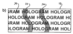
図3のc)は結合積層体の上面図を示す。図3のc)においては、基材18の元のマイクロ構造におけるホログラフィック情報を保持するストライプ22、24が明確に視認できる。
FIG. 3 c) shows a top view of the bonded stack. In c) of FIG. 3, the
本発明の実施形態による多種多様な形状及びグラフィカルモチーフを形成するために、様々なパターン形成技法が用いられることが当然理解されよう。本発明は同様に、図2及び図3に示されるような「S」ストライプに限定されない。むしろ熱可塑性体28は、図4に示される連続ドット30、直線32、ランダムドット34、組織化されたドット36、組紐飾りパターン38、一般的なモチーフ40、ベタ領域要素42などの多種多様な形状やモチーフとともに提供できる。
It will be appreciated that a variety of patterning techniques may be used to form a wide variety of shapes and graphical motifs according to embodiments of the present invention. The present invention is likewise not limited to “S” stripes as shown in FIGS. Rather, the thermoplastic 28 has a wide variety of dots such as the continuous dots 30, straight lines 32, random dots 34, organized
次に図5を参照すると、図4の一般的なモチーフ40からなる想定されるパターン(模様)の一例が提供される。図5の詳細により確認できるように、上記パターンは模様付けされた小さいドット/要素46の配列から形成される。a1、a2、aj、b1、b2、及びc1、c2で示される各ドットの座標位置及び寸法は、容易に識別可能なモチーフの視覚的表示を組み合わせて提供するだけでなく、所定の空間定位を経て、例えば、構造の回折パターンの観察を通じたレーダ支援技法などの電磁波検出を介して容易に検出可能な上記ドット/要素46の配置を提供するために用いられる。もちろん、各特定の要素の特徴的なサイズ及び上記要素間の間隔はさまざまであり、要素のグラフィカルな終端処理を採用する実際の技法にある程度依存する。 Referring now to FIG. 5, an example of an assumed pattern consisting of the general motif 40 of FIG. 4 is provided. As can be seen from the details of FIG. 5, the pattern is formed from an array of patterned small dots / elements 46. The coordinate positions and dimensions of each dot, denoted a1, a2, aj, b1, b2, and c1, c2, not only provide a combination of easily identifiable visual representations of motifs, but also provide a predetermined spatial orientation. Via, for example, it is used to provide an arrangement of the dots / elements 46 that is easily detectable via electromagnetic wave detection, such as radar assisted techniques through observation of the diffraction pattern of the structure. Of course, the characteristic size of each particular element and the spacing between the elements will vary and will depend in part on the actual technique employing the graphical termination of the element.
例として、標準の光学リソグラフィク及びマスキング技法、及びプリント技法は、数ミクロン程度の精密さで使用でき、1μmの領域における特徴を提供可能である。実際、高度な光学リソグラフィック技法、一般的に紫外線を用いる技法、又は電子ビーム書き込み技法を使用して、100nmほどの小さな想定される要素の詳細の描写が可能である。このように、レリーフ構造の詳細は、放射そのものの特徴的なサイズに適合するサイズであり得る。 By way of example, standard optical lithographic and masking techniques, and printing techniques can be used with a precision on the order of a few microns and can provide features in the 1 μm region. In fact, details of possible elements as small as 100 nm can be described using advanced optical lithographic techniques, generally using ultraviolet light, or electron beam writing techniques. Thus, the details of the relief structure can be sized to match the characteristic size of the radiation itself.
理解されるように、さまざまな要素間の間隔を適切に選択することで、例えば身分確認資料などの追加のレーザ支援書き込み及び/又はレーザ支援パーソナル化が容易に実現できる。更にまた、上記要素の密度は、構造の透明性を制御する。各要素は裸眼で観測できるよりも一般的に小さい寸法で容易に提供できるため、金属要素を採用する構造でさえも半透明の外観を示す。 As will be appreciated, additional laser-assisted writing and / or laser-assisted personalization, such as identification material, can be readily achieved by appropriately selecting the spacing between the various elements. Furthermore, the density of the elements controls the transparency of the structure. Since each element can be easily provided in generally smaller dimensions than can be observed with the naked eye, even structures employing metal elements exhibit a translucent appearance.
このようなモチーフの提供は、基材の本体から上記モチーフの除去を試みると個々の要素間における空間関係の変形を導き、電磁波や何らかのレーダ支援技法による後の調査の際に容易に識別できるため、偽造などのさらなる利用に対し、その限りにおいて特有の利点が分かる。従って、たとえモチーフ48の変形が裸眼により容易に識別できない場合でも、個々の要素間における空間関係のさらなる調査により、何らかの変形が生じてモチーフを保持するセキュリティラベル/構造の悪用が試みられたことが示唆される。
The provision of such motifs can lead to deformation of the spatial relationship between individual elements when attempting to remove the motif from the body of the substrate, and can be easily identified in subsequent investigations using electromagnetic waves or some radar-assisted technique. As far as further use such as counterfeiting is concerned, the unique advantages can be seen. Therefore, even if the deformation of the
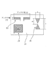
本発明による基材内埋め込まれた金属処理された構造は、電子部品を備える場合があることが当然理解されよう。図6には、幅Wと長さLを有するダイポールアンテナ52、誘導子型アンテナ54、及び図示のように各寸法e、wb、及びe/2を有する三角形のハーフループを含むバタフライアンテナ56を形成する金属部品を備えた基材50が示される。この技法により実現されうる上記特定要素のサイズは、例えばTHzに至るまでの広帯域の周波数内で動作する種々の基本的な電気的要素を提供できる限りにおいて有利な特徴を提供する。本発明において採用する方法では、1um程度又はそれより小さいサイズの要素に対して、いわゆる光素子及びメタマテリアルデバイスのカテゴリから集積回路(IC)の生産を可能にする。
It will be appreciated that a metallized structure embedded in a substrate according to the present invention may comprise electronic components. FIG. 6 shows a
さらにまた、構造全体内で特徴となるプリントエレクトロニクスを組み込む際に役立つように、上記要素は適当な半導体又は誘電材料から容易に形成され得る。 Furthermore, the elements can be easily formed from a suitable semiconductor or dielectric material to help in incorporating the printed electronics that are featured within the overall structure.
図7は、基材58内に埋め込まれた金属部品の他の構成を示す。基材58は、集積回路又は電子機器60とそれらのための導電性接触子62を備える。上記結合構造の提供は、表面実装型デバイスに採用される又はプリントエレクトロニックやナノエンボス加工された電子要素などのアプリケーションに採用される通常の電子配置に特に有用である。
FIG. 7 shows another configuration of the metal component embedded in the
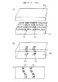
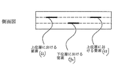
最後に図8a及び図8bを参照すると、熱可塑性バルク体64内の異なる階層に設けられた種々の金属要素が示されている。すなわち、図8aの正面斜視図及び図8bの側面図により、要素66、68の両方はバルク体64内の上位層に設けられ、一方要素70は下位層に設けられることが理解されよう。
Finally, referring to FIGS. 8 a and 8 b, various metal elements provided at different levels in the thermoplastic bulk body 64 are shown. That is, it will be appreciated from the front perspective view of FIG. 8a and the side view of FIG. 8b that both
本発明は、階層構造における層の表面上にレリーフパターンを形成し、次に、上記階層構造の後続処理の際に下層のレリーフパターンの保護する保護固定層を上記レリーフパターンの少なくとも一部に形成する、階層構造の一部としてレリーフパターンを形成する方法を提供することが理解されよう。その結果、上記レリーフの少なくとも一部には、例えばレリーフパターンが設けられる積層構造を形成する場合などの上記階層構造の後続処理の際にレリーフパターンの特性を保持する保護固定層が設けられている、基材の表面上に形成されたレリーフパターンを有する基材を含む階層構造を提供する。 The present invention forms a relief pattern on the surface of the layer in the hierarchical structure, and then forms a protective fixing layer that protects the underlying relief pattern on at least a part of the relief pattern during subsequent processing of the hierarchical structure. It will be appreciated that a method of forming a relief pattern as part of a hierarchical structure is provided. As a result, at least a part of the relief is provided with a protective fixing layer that retains the characteristics of the relief pattern during subsequent processing of the hierarchical structure, such as when forming a laminated structure provided with a relief pattern. Providing a hierarchical structure comprising a substrate having a relief pattern formed on the surface of the substrate.
本発明は、前述の実施形態の詳細に限定されることはなく、任意の適切な材料が基材のレリーフ構造の固定に用いられ得る限りにおいて、金属要素はいずれの特定のレリーフパターンを含まない場合があることが当然理解されよう。そのような実施形態において、本発明は、層が「固定」され、金属処理されているか否かに限らず存在しないレリーフパターンを示すとき、構造のその部分は僅かにグラディエント(negligible gradient)なレリーフパターンを備えると考えられる。 The present invention is not limited to the details of the foregoing embodiments, and the metal elements do not include any particular relief pattern, as long as any suitable material can be used to secure the relief structure of the substrate. It will be understood that there are cases. In such an embodiment, the present invention provides a relief with a slightly gradient of that portion of the structure when presenting a relief pattern that does not exist, whether or not the layer is “fixed” and metallized. It is considered to have a pattern.
Claims (44)
Applications Claiming Priority (3)
| Application Number | Priority Date | Filing Date | Title |
|---|---|---|---|
| GBGB0902000.9A GB0902000D0 (en) | 2009-02-09 | 2009-02-09 | Micro-relief structures |
| GB0902000.9 | 2009-02-09 | ||
| PCT/EP2010/051521 WO2010089399A1 (en) | 2009-02-09 | 2010-02-08 | Micro-relief structures |
Publications (2)
| Publication Number | Publication Date |
|---|---|
| JP2012517610A true JP2012517610A (en) | 2012-08-02 |
| JP2012517610A5 JP2012517610A5 (en) | 2013-03-28 |
Family
ID=40469716
Family Applications (1)
| Application Number | Title | Priority Date | Filing Date |
|---|---|---|---|
| JP2011548722A Pending JP2012517610A (en) | 2009-02-09 | 2010-02-08 | Micro relief structure |
Country Status (14)
| Country | Link |
|---|---|
| US (1) | US20130189489A1 (en) |
| EP (1) | EP2393653A1 (en) |
| JP (1) | JP2012517610A (en) |
| KR (1) | KR20110119786A (en) |
| CN (1) | CN102307719B (en) |
| AU (1) | AU2010210070B2 (en) |
| BR (1) | BRPI1008128A2 (en) |
| CA (1) | CA2751013A1 (en) |
| GB (1) | GB0902000D0 (en) |
| IL (1) | IL214329A0 (en) |
| MX (1) | MX2011008103A (en) |
| RU (1) | RU2566928C2 (en) |
| WO (1) | WO2010089399A1 (en) |
| ZA (1) | ZA201105633B (en) |
Families Citing this family (4)
| Publication number | Priority date | Publication date | Assignee | Title |
|---|---|---|---|---|
| ITRM20130007A1 (en) | 2013-01-07 | 2014-07-08 | Zecca Dello Ist Poligrafico | METHOD OF REALIZATION OF DIFFRACTIVE METALLIC MICROELEMENTS VARIABLE IN A LAMINABLE PLASTIC BODY. |
| EP3134249A1 (en) | 2014-04-23 | 2017-03-01 | IQ Structures S.r.o. | Method of manufacturing laminate and the laminate |
| FR3065557B1 (en) * | 2017-04-19 | 2022-08-19 | Oberthur Technologies | METHOD FOR MANUFACTURING A SECURITY DEVICE IN THE FORM OF SUPERIMPOSED LAYERS, AND METHOD FOR AUTHENTICATING SUCH A SECURITY DEVICE |
| PL3888929T3 (en) | 2020-03-31 | 2023-01-16 | Pentacomp Pte. Ltd. | A method of manufacturing a discretized optical security microstructure on a substrate and a shim for use in the method |
Citations (11)
| Publication number | Priority date | Publication date | Assignee | Title |
|---|---|---|---|---|
| JPS58198007A (en) * | 1982-05-14 | 1983-11-17 | Ricoh Co Ltd | Diffraction grating having protective film |
| JPS63108374A (en) * | 1986-10-25 | 1988-05-13 | Dainippon Printing Co Ltd | Duplicating method for hologram |
| JPH06214117A (en) * | 1992-08-04 | 1994-08-05 | Nippondenso Co Ltd | Hologram and its sticking method |
| GB2300379A (en) * | 1995-04-05 | 1996-11-06 | Applied Holographics | Application to substrates of elements or films which have a surface relief pattern providing an optically variable effect |
| JP2005007624A (en) * | 2003-06-17 | 2005-01-13 | Toppan Printing Co Ltd | Transfer sheet and its manufacturing method |
| JP2005313354A (en) * | 2004-04-27 | 2005-11-10 | Dainippon Printing Co Ltd | Information recording medium, recording method therefor, and recording apparatus therefor |
| JP2006272816A (en) * | 2005-03-30 | 2006-10-12 | National Printing Bureau | Printed matter and its reading out device |
| JP2006330487A (en) * | 2005-05-27 | 2006-12-07 | Nidec Sankyo Corp | Optical element, method of manufacturing optical element, and optical desk device |
| US20070089831A1 (en) * | 2005-10-17 | 2007-04-26 | Celerino Florentino | Card with hologram formed over magnetic strip |
| JP2007148074A (en) * | 2005-11-29 | 2007-06-14 | Dainippon Printing Co Ltd | Light diffracting sheet |
| JP2008049643A (en) * | 2006-08-28 | 2008-03-06 | Toppan Printing Co Ltd | Forgery preventive magnetic tape transfer sheet and card |
Family Cites Families (10)
| Publication number | Priority date | Publication date | Assignee | Title |
|---|---|---|---|---|
| EP0201323B1 (en) * | 1985-05-07 | 1994-08-17 | Dai Nippon Insatsu Kabushiki Kaisha | Article incorporating a transparent hologramm |
| US5510171A (en) * | 1995-01-19 | 1996-04-23 | Minnesota Mining And Manufacturing Company | Durable security laminate with hologram |
| DE10044465A1 (en) * | 2000-09-08 | 2002-03-21 | Giesecke & Devrient Gmbh | Data carrier with an optically variable element |
| US6902807B1 (en) * | 2002-09-13 | 2005-06-07 | Flex Products, Inc. | Alignable diffractive pigment flakes |
| US6752868B2 (en) * | 2002-07-31 | 2004-06-22 | Mcnc Research & Development Institute | Layer-by-layer assembly of photonic crystals |
| DE10333704B4 (en) * | 2003-07-23 | 2009-12-17 | Ovd Kinegram Ag | Security element for RF identification |
| WO2005024699A2 (en) * | 2003-09-03 | 2005-03-17 | Digimarc Corporation | Identification document with optical memory and related method of manufacture |
| CZ2004234A3 (en) | 2004-02-12 | 2005-03-16 | Optaglio S. R. O. | Metallic identification chip and process for producing thereof |
| US7982930B2 (en) * | 2004-12-03 | 2011-07-19 | Illinois Tool Works Inc | Preserved and enhanced holographic and optically variable devices and method for making the same |
| DE102006055787A1 (en) * | 2006-04-13 | 2007-10-18 | Giesecke & Devrient Gmbh | ID card with contoured relief structure and corresponding manufacturing process |
-
2009
- 2009-02-09 GB GBGB0902000.9A patent/GB0902000D0/en not_active Ceased
-
2010
- 2010-02-08 EP EP10703844A patent/EP2393653A1/en not_active Withdrawn
- 2010-02-08 MX MX2011008103A patent/MX2011008103A/en not_active Application Discontinuation
- 2010-02-08 BR BRPI1008128A patent/BRPI1008128A2/en not_active IP Right Cessation
- 2010-02-08 CA CA2751013A patent/CA2751013A1/en not_active Abandoned
- 2010-02-08 WO PCT/EP2010/051521 patent/WO2010089399A1/en active Application Filing
- 2010-02-08 RU RU2011137153/12A patent/RU2566928C2/en not_active IP Right Cessation
- 2010-02-08 AU AU2010210070A patent/AU2010210070B2/en not_active Expired - Fee Related
- 2010-02-08 KR KR1020117020891A patent/KR20110119786A/en not_active Application Discontinuation
- 2010-02-08 JP JP2011548722A patent/JP2012517610A/en active Pending
- 2010-02-08 CN CN201080007141.6A patent/CN102307719B/en not_active Expired - Fee Related
- 2010-02-08 US US13/147,328 patent/US20130189489A1/en not_active Abandoned
-
2011
- 2011-07-28 IL IL214329A patent/IL214329A0/en unknown
- 2011-07-29 ZA ZA2011/05633A patent/ZA201105633B/en unknown
Patent Citations (11)
| Publication number | Priority date | Publication date | Assignee | Title |
|---|---|---|---|---|
| JPS58198007A (en) * | 1982-05-14 | 1983-11-17 | Ricoh Co Ltd | Diffraction grating having protective film |
| JPS63108374A (en) * | 1986-10-25 | 1988-05-13 | Dainippon Printing Co Ltd | Duplicating method for hologram |
| JPH06214117A (en) * | 1992-08-04 | 1994-08-05 | Nippondenso Co Ltd | Hologram and its sticking method |
| GB2300379A (en) * | 1995-04-05 | 1996-11-06 | Applied Holographics | Application to substrates of elements or films which have a surface relief pattern providing an optically variable effect |
| JP2005007624A (en) * | 2003-06-17 | 2005-01-13 | Toppan Printing Co Ltd | Transfer sheet and its manufacturing method |
| JP2005313354A (en) * | 2004-04-27 | 2005-11-10 | Dainippon Printing Co Ltd | Information recording medium, recording method therefor, and recording apparatus therefor |
| JP2006272816A (en) * | 2005-03-30 | 2006-10-12 | National Printing Bureau | Printed matter and its reading out device |
| JP2006330487A (en) * | 2005-05-27 | 2006-12-07 | Nidec Sankyo Corp | Optical element, method of manufacturing optical element, and optical desk device |
| US20070089831A1 (en) * | 2005-10-17 | 2007-04-26 | Celerino Florentino | Card with hologram formed over magnetic strip |
| JP2007148074A (en) * | 2005-11-29 | 2007-06-14 | Dainippon Printing Co Ltd | Light diffracting sheet |
| JP2008049643A (en) * | 2006-08-28 | 2008-03-06 | Toppan Printing Co Ltd | Forgery preventive magnetic tape transfer sheet and card |
Also Published As
| Publication number | Publication date |
|---|---|
| AU2010210070A1 (en) | 2011-08-18 |
| MX2011008103A (en) | 2011-11-18 |
| US20130189489A1 (en) | 2013-07-25 |
| AU2010210070B2 (en) | 2015-11-12 |
| CA2751013A1 (en) | 2010-08-12 |
| KR20110119786A (en) | 2011-11-02 |
| CN102307719B (en) | 2015-11-25 |
| RU2566928C2 (en) | 2015-10-27 |
| BRPI1008128A2 (en) | 2016-03-08 |
| GB0902000D0 (en) | 2009-03-11 |
| CN102307719A (en) | 2012-01-04 |
| WO2010089399A1 (en) | 2010-08-12 |
| ZA201105633B (en) | 2016-07-27 |
| RU2011137153A (en) | 2013-03-27 |
| IL214329A0 (en) | 2011-09-27 |
| EP2393653A1 (en) | 2011-12-14 |
Similar Documents
| Publication | Publication Date | Title |
|---|---|---|
| JP5186378B2 (en) | Multilayer body and method for producing the same | |
| RU2390808C2 (en) | Multilayer body and method of making multilayer body | |
| JP5124272B2 (en) | Metallized security element | |
| RU2517134C2 (en) | Making of protection element and retransfer film | |
| EP1294576B1 (en) | A security device | |
| JP6649275B2 (en) | Multilayer body and method for producing the same | |
| RU2015133719A (en) | PROTECTIVE DEVICE AND METHOD FOR ITS MANUFACTURE | |
| EP2359196B1 (en) | Security device, method and article | |
| JP2006501659A5 (en) | ||
| JP5551171B2 (en) | Packaging and forming method | |
| JP2012517610A (en) | Micro relief structure | |
| US20230021631A1 (en) | Laminate, card, method of manufacturing card, method of producing card, card information recording sheet and card including the same | |
| US20190249013A1 (en) | Flakes with undulate borders and methods of forming thereof | |
| US20220055363A1 (en) | Method for producing a film intermediate product, film intermediate product and method for producing a product | |
| US8526086B2 (en) | Metallised film and process for its manufacture | |
| TWI552087B (en) | Multi-layer body for security element agalnst counterfeiting of security document | |
| JP2012517610A5 (en) | ||
| US20210010139A1 (en) | Metallic sheet with deposited structured images and method of manufacture | |
| JP5040609B2 (en) | Security optical device manufacturing method and security optical device | |
| JP2015121675A (en) | Display body |
Legal Events
| Date | Code | Title | Description |
|---|---|---|---|
| A521 | Request for written amendment filed |
Free format text: JAPANESE INTERMEDIATE CODE: A523 Effective date: 20130205 |
|
| A621 | Written request for application examination |
Free format text: JAPANESE INTERMEDIATE CODE: A621 Effective date: 20130205 |
|
| A977 | Report on retrieval |
Free format text: JAPANESE INTERMEDIATE CODE: A971007 Effective date: 20130822 |
|
| A131 | Notification of reasons for refusal |
Free format text: JAPANESE INTERMEDIATE CODE: A131 Effective date: 20130911 |
|
| A601 | Written request for extension of time |
Free format text: JAPANESE INTERMEDIATE CODE: A601 Effective date: 20131211 |
|
| A602 | Written permission of extension of time |
Free format text: JAPANESE INTERMEDIATE CODE: A602 Effective date: 20131218 |
|
| A601 | Written request for extension of time |
Free format text: JAPANESE INTERMEDIATE CODE: A601 Effective date: 20140110 |
|
| A602 | Written permission of extension of time |
Free format text: JAPANESE INTERMEDIATE CODE: A602 Effective date: 20140120 |
|
| A601 | Written request for extension of time |
Free format text: JAPANESE INTERMEDIATE CODE: A601 Effective date: 20140210 |
|
| A602 | Written permission of extension of time |
Free format text: JAPANESE INTERMEDIATE CODE: A602 Effective date: 20140218 |
|
| A521 | Request for written amendment filed |
Free format text: JAPANESE INTERMEDIATE CODE: A523 Effective date: 20140311 |
|
| A02 | Decision of refusal |
Free format text: JAPANESE INTERMEDIATE CODE: A02 Effective date: 20140910 |
|
| A521 | Request for written amendment filed |
Free format text: JAPANESE INTERMEDIATE CODE: A523 Effective date: 20150109 |
|
| A911 | Transfer to examiner for re-examination before appeal (zenchi) |
Free format text: JAPANESE INTERMEDIATE CODE: A911 Effective date: 20150310 |
|
| A912 | Re-examination (zenchi) completed and case transferred to appeal board |
Free format text: JAPANESE INTERMEDIATE CODE: A912 Effective date: 20150424 |