JP2012248035A - Touch panel system and electronic apparatus using the same - Google Patents
Touch panel system and electronic apparatus using the same Download PDFInfo
- Publication number
- JP2012248035A JP2012248035A JP2011119774A JP2011119774A JP2012248035A JP 2012248035 A JP2012248035 A JP 2012248035A JP 2011119774 A JP2011119774 A JP 2011119774A JP 2011119774 A JP2011119774 A JP 2011119774A JP 2012248035 A JP2012248035 A JP 2012248035A
- Authority
- JP
- Japan
- Prior art keywords
- touch panel
- sensitivity
- touch
- touch operation
- panel system
- Prior art date
- Legal status (The legal status is an assumption and is not a legal conclusion. Google has not performed a legal analysis and makes no representation as to the accuracy of the status listed.)
- Granted
Links
Images


Abstract
Description
本発明は、タッチパネルシステムに関し、特に、人指等が接触すること無く、接近することによっても、タッチ操作が可能である高感度なタッチパネルシステムおよびそれを用いた電子機器に関するものである。 The present invention relates to a touch panel system, and more particularly to a highly sensitive touch panel system capable of performing a touch operation even when a human finger or the like approaches without touching it, and an electronic apparatus using the touch panel system.
現在、スマートフォン等の携帯情報機器、自動券売機等の自動販売機を始めとする様々な電子機器に、タッチパネルシステムの搭載が急速に進んでいる。タッチパネルにおいては、抵抗膜方式等の方式が広く普及しているが、入力される指先が複数の場合の検出が可能である投影型静電容量方式の普及も進みつつある。 Currently, touch panel systems are rapidly being installed in various electronic devices such as portable information devices such as smartphones and vending machines such as vending machines. In the touch panel, a method such as a resistive film method is widely used, but a projection capacitive method capable of detecting when a plurality of fingertips are input is also spreading.
抵抗膜方式のタッチパネル、例えば4線式抵抗膜方式タッチパネルの場合においては、前後方向、左右方向に電極が付いた二つの抵抗膜が上下に向かい合って構成されている。上下の抵抗膜の間には、セパレータを使用して隙間が設けられ、通常状態では抵抗膜同士が接触しないようになっている。人指等でのタッチパネルへの接触があった場合、図6に示すように上下の抵抗膜が接触し、その位置の電圧を反対側の抵抗膜経由で測定することで、接触位置を求めることができる。即ち、抵抗膜方式については、タッチ操作をするために、タッチパネルへの接触が必須である。 In the case of a resistive film type touch panel, for example, a 4-wire resistive film type touch panel, two resistive films with electrodes in the front-rear direction and the left-right direction are configured to face each other vertically. A gap is provided between the upper and lower resistance films using a separator so that the resistance films do not contact each other in a normal state. When the finger touches the touch panel, the upper and lower resistive films come into contact with each other as shown in FIG. 6, and the voltage at that position is measured via the opposite resistive film to obtain the contact position. Can do. That is, for the resistive film method, in order to perform a touch operation, contact with the touch panel is essential.
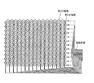
他方、投影型静電容量方式のタッチパネルでは、タッチパネルを上方から見たとき、基本的にその電極の形状と配置とは、マトリクス状に正方形形状の電極が連続的に配置されたものとなる。この投影型静電容量方式の従来の電極の形状を図7に示す。図8は、第1の電極および第2の電極の形状と配置とを示す図である。図8に示されるように、第1の電極と第2の電極とは等しい形状を有しており、多数のダイヤ形状の電極が連続的に配置されたものであることが分かる。 On the other hand, in the projected capacitive touch panel, when the touch panel is viewed from above, the shape and arrangement of the electrodes are basically such that square electrodes are continuously arranged in a matrix. FIG. 7 shows the shape of a conventional electrode of the projected capacitance type. FIG. 8 is a diagram showing the shape and arrangement of the first electrode and the second electrode. As shown in FIG. 8, it can be seen that the first electrode and the second electrode have the same shape, and a large number of diamond-shaped electrodes are continuously arranged.
このような投影型静電容量方式のタッチパネルは、電極間の静電容量の変化を捕えるものであり、縦横に走っている電極に人指等が近づくと、指と電極間の静電容量が変化する。そして、縦横のどのライン間の静電容量の変化が大きいかを調べると、どの交点に近づいたかが分かることになる(図9参照)。 Such a projected capacitive touch panel captures changes in capacitance between electrodes, and when a finger or the like approaches an electrode running vertically and horizontally, the capacitance between the finger and the electrode increases. Change. Then, by examining which of the vertical and horizontal lines the capacitance change is large, it can be seen which intersection point is approached (see FIG. 9).
このような、投影型静電容量方式においては、人指等が接触すること無く、単に接近することによっても、高感度なタッチパネルシステムであれば、タッチ操作が検出可能である。 In such a projected capacitive system, a touch operation can be detected by a touch panel system with high sensitivity even by simply approaching without touching a human finger or the like.
但し、上記のように、高感度で、人指等が接触すること無くタッチ操作が可能なシステムでは、意識的にタッチ操作を行っていない場合にも、タッチパネルに人指が近づくことにより、タッチ操作とみなされて動作してしまう恐れがある。 However, as described above, in a system that allows high-sensitivity touch operations without touching human fingers, etc., even when the touch operation is not consciously performed, the touch of the finger on the touch panel There is a risk that it will be considered as an operation.
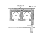
特許文献1においては、図10に示すように、SW1およびSW2からなる接触用センサ(第1接触センサ)に加え、接触用センサに近接してSW3からなるダミーセンサ(第2接触センサ)を設置し、ダミーセンサによって意図しない接触による誤操作時の接触を検出するタッチパネルが開示されている。 In Patent Document 1, as shown in FIG. 10, in addition to the contact sensor (first contact sensor) composed of SW1 and SW2, a dummy sensor (second contact sensor) composed of SW3 is installed close to the contact sensor. And the touch panel which detects the contact at the time of incorrect operation by the contact which is not intended by the dummy sensor is disclosed.
上述のように、特許文献1による接触センサでは、意図しない接触による誤操作時の接触については、ダミーセンサ(第2接触センサ)により接触の検出が可能である。しかしながら、上述の投影型静電容量方式のように、人指等が接触すること無く、接近することによってもタッチ操作が可能なタッチパネルシステムの場合では、ダミーセンサに接触せずとも、意図せずタッチ操作が検出されることになる。 As described above, in the contact sensor according to Patent Document 1, the contact at the time of an erroneous operation due to an unintended contact can be detected by a dummy sensor (second contact sensor). However, in the case of a touch panel system in which a touch operation can be performed by approaching without touching a human finger or the like as in the above-described projected capacitive method, it is not intended even if the dummy sensor is not touched. A touch operation is detected.
本発明の目的は、人指等が接触すること無く、接近することによってもタッチ操作が可能な高感度なタッチパネルシステムに関して、人指等の意図しない接近による誤操作を防止することが可能なタッチパネルシステムを提供することにある。 An object of the present invention relates to a high-sensitivity touch panel system that can be touch-operated even by approaching without touching a human finger or the like, and capable of preventing erroneous operation due to unintended approach of a human finger or the like Is to provide.
上記の課題を解決するために、本発明のタッチパネルシステムは、投影型静電容量方式のタッチパネルと、前記タッチパネルからの信号を受信し、その受信信号に基づいて使用者によるタッチ操作を検出するタッチパネルコントローラとを有しており、前記タッチパネルコントローラは、タッチパネルにおいて検出されるタッチ操作の感度の変更を行うタッチ操作感度変更手段を有していることを特徴としている。 In order to solve the above problems, a touch panel system of the present invention includes a projected capacitive touch panel and a touch panel that receives a signal from the touch panel and detects a touch operation by a user based on the received signal. The touch panel controller has a touch operation sensitivity changing means for changing the sensitivity of the touch operation detected on the touch panel.
上記の構成によれば、前記タッチパネルコントローラは、タッチ操作の感度の変更を行うタッチ操作感度変更手段を有しているため、タッチ操作の感度を低下させる変更を行うことで、意図せず人指等がタッチパネルに接近した場合等に、タッチ操作として動作を行わないようにすることが可能となる。逆に、タッチ操作の感度を向上させる変更を行うことで、手袋をしたままでのタッチ操作や、非接触でのタッチ操作を可能とする。 According to the above configuration, the touch panel controller includes the touch operation sensitivity changing unit that changes the sensitivity of the touch operation. It is possible to prevent the operation from being performed as a touch operation when, for example, the user approaches the touch panel. Conversely, by making a change that improves the sensitivity of the touch operation, it is possible to perform a touch operation while wearing a glove or a non-contact touch operation.
また、上記タッチパネルシステムでは、前記タッチパネルコントローラは、前記タッチパネルからの受信信号を複数回積算し、その積算された信号値をタッチ操作検出閾値と比較することでタッチ操作を検出するものであり、前記タッチ操作感度変更手段は、前記タッチ操作の感度の変更を、前記受信信号の受信積算回数を変更することにより行う構成とすることができる。 Further, in the touch panel system, the touch panel controller integrates a plurality of received signals from the touch panel, and detects a touch operation by comparing the accumulated signal value with a touch operation detection threshold. The touch operation sensitivity changing means may be configured to change the sensitivity of the touch operation by changing the number of times of reception integration of the received signal.
上記の構成によれば、前記受信積算回数を減らすことで、タッチ操作の感度を低下させる変更を行うことができる。あるいは、前記受信積算回数を増やすことで、タッチ操作の感度を向上させる変更を行うこともできる。 According to said structure, the change which reduces the sensitivity of touch operation can be performed by reducing the said frequency | count of reception integration. Or the change which improves the sensitivity of touch operation can also be performed by increasing the said reception integration frequency.
また、上記タッチパネルシステムでは、前記タッチ操作の感度の変更指示モードへの移行を、ボタン操作により行う構成、あるいは、前記タッチ操作の感度の変更指示モードへの移行を、ソフトウェアにより行う構成とすることができる。 In the touch panel system, the transition to the touch operation sensitivity change instruction mode is performed by a button operation, or the transition to the touch operation sensitivity change instruction mode is performed by software. Can do.
また、上記タッチパネルシステムでは、前記タッチ操作の感度の変更を、ユーザインタフェイスを介して行う構成とすることができる。 In the touch panel system, the sensitivity of the touch operation can be changed via a user interface.
また、上記タッチパネルシステムでは、前記タッチ操作の感度の変更は、予め設定されている複数の感度の中から選択可能である構成とすることができる。 In the touch panel system, the change in sensitivity of the touch operation can be selected from a plurality of preset sensitivities.
また、上記タッチパネルシステムでは、前記タッチ操作の感度の変更によって、手袋装着によるタッチ操作の可/不可が切り替え可能である構成、あるいは、非接触でのタッチ操作の可/不可が切り替え可能である構成とすることができる。 Further, in the touch panel system, a configuration in which the touch operation by glove wearing can be switched by changing the sensitivity of the touch operation, or a configuration in which the touch operation by non-contact can be switched can be switched. It can be.
また、上記タッチパネルシステムでは、前記タッチパネルのセンサ部を構成する電極が、透明電極である構成とすることができる。 Moreover, in the said touch panel system, the electrode which comprises the sensor part of the said touch panel can be set as the structure which is a transparent electrode.
また、上記の課題を解決するために、本発明の電子機器は、上記記載の何れかのタッチパネルシステムを備えたことを特徴としている。 In order to solve the above-described problems, an electronic apparatus according to the present invention includes any one of the touch panel systems described above.
また、上記電子機器では、前記タッチパネルが、表示装置の表示画面上に重畳配置される構成とすることができる。 Moreover, in the said electronic device, the said touch panel can be set as the structure superimposed on the display screen of a display apparatus.
また、上記電子機器では、前記表示装置が、液晶ディスプレイ、プラズマディスプレイ、有機ELディスプレイ、および電界放出ディスプレイの何れかである構成とすることができる。 In the electronic apparatus, the display device may be any one of a liquid crystal display, a plasma display, an organic EL display, and a field emission display.
本発明のタッチパネルシステムにおいてば、タッチパネルからの信号を受信し、その受信信号に基づいて使用者によるタッチ操作を検出するタッチパネルコントローラが、タッチ操作の感度の変更を行うタッチ操作感度変更手段を有している。それゆえ、タッチ操作の感度を低下させる変更を行うことで、意図せず人指等がタッチパネルに接近した場合等に、タッチ操作として動作を行わないようにすることが可能となる。逆に、タッチ操作の感度を向上させる変更を行うことで、手袋をしたままでのタッチ操作や、非接触でのタッチ操作を可能とする。 In the touch panel system of the present invention, the touch panel controller that receives a signal from the touch panel and detects a touch operation by the user based on the received signal has touch operation sensitivity changing means for changing the sensitivity of the touch operation. ing. Therefore, by making a change that lowers the sensitivity of the touch operation, it is possible to prevent the operation as a touch operation when a human finger or the like approaches the touch panel unintentionally. Conversely, by making a change that improves the sensitivity of the touch operation, it is possible to perform a touch operation while wearing a glove or a non-contact touch operation.
以下に、本発明のタッチパネルシステムの実施の形態について、図面を参照しながら説明する。本実施の形態のタッチパネルシステムは投影型静電容量方式を採用するものである。図1は、本実施の形態に係るタッチパネルシステム1の基本構成を示す図である。 Embodiments of a touch panel system of the present invention will be described below with reference to the drawings. The touch panel system of the present embodiment employs a projected capacitive system. FIG. 1 is a diagram showing a basic configuration of a touch panel system 1 according to the present embodiment.
図1に示すように、タッチパネルシステム1は、タッチパネル10とタッチパネルコントローラ20とからなる。タッチパネル10は、使用者がタッチ操作を行うことにより信号を入力するセンサ11を備えている。タッチパネルコントローラ20は、センサ11からの信号を受信する入力端子と、入力端子に入力された信号を元に、座標値を出力する座標検出手段21と、座標検出手段21からの座標情報を一定間隔で取り込み、表示装置に出力等を行うCPU22とからなる。座標検出手段21は、タッチ操作の感度の変更を行うタッチ操作感度変更手段23を有している。
As shown in FIG. 1, the touch panel system 1 includes a
尚、本実施の形態におけるタッチパネルシステム1に配置されているセンサ11は、静電容量方式センサであり、使用者がタッチパネル10にタッチ操作した際、センサ11を構成している電極が図1に示すドライブライン−センスライン間の容量値の変化を検出する。
Note that the sensor 11 arranged in the touch panel system 1 in the present embodiment is a capacitive sensor, and when the user touches the
タッチパネル10は、M本のドライブラインとL本のセンスラインとからなり、その交差箇所に静電容量方式によるセンサ11を構成する。タッチ操作の座標検出動作では、ドライブラインをスキャンしつつ、タッチ操作によるセンサの容量値の変化をセンスラインにて読み取ることにより、タッチ操作された箇所の座標を検出する。この際、検出される容量値の変化値が小さい場合を考慮して、読み取り動作を複数回行い、タッチパネルからの受信信号を上記複数回の読み取り動作に対応させて複数回積算して信号値を増大させる操作が行われている。
The
図2に、この読み取り操作を複数回行っている状況を示す。図2(a)は上記読み取り操作が8回行われている場合を示しており、図2(b)は上記読み取り操作が3回行われている場合を示している。図2(a)では、読み取り操作が8回行われた結果の信号積算値がタッチ操作検出閾値を超えている。このように、タッチ操作の検出は、信号値がタッチ操作検出閾値を超えた場合に、使用者がタッチ操作を行ったと判定される。 FIG. 2 shows a situation where this reading operation is performed a plurality of times. FIG. 2A shows a case where the reading operation is performed eight times, and FIG. 2B shows a case where the reading operation is performed three times. In FIG. 2A, the signal integrated value resulting from the eight reading operations exceeds the touch operation detection threshold. Thus, the detection of the touch operation is determined that the user has performed the touch operation when the signal value exceeds the touch operation detection threshold.
但し、この判定については、上述したように、投影型静電容量方式タッチパネルシステムにおいては、人指等が接触すること無く、接近することによっても、高感度なタッチパネルシステムであれば、意図せずにタッチ操作が検出されてしまう恐れがある。この課題の解消のために、タッチ操作の感度の変更を行うことが考えられる。 However, as described above, this determination is not intended for a projected capacitive touch panel system as long as it is a touch panel system with high sensitivity even when a finger or the like approaches without touching it. Touch operation may be detected. In order to solve this problem, it is conceivable to change the sensitivity of the touch operation.
図3は、本発明によるタッチパネルシステムのタッチ操作感度変更処理をフローチャートで示したものである。 FIG. 3 is a flowchart showing touch operation sensitivity changing processing of the touch panel system according to the present invention.
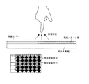
使用者がタッチ操作感度変更を指示する場合(F201)、その変更指示モードへの移行方法は、使用者がタッチ操作感度変更処理ボタンを操作してタッチパネルシステムの起動時表示ページからタッチ操作感度変更のためのアプリケーションを起動したり、タッチ操作感度変更表示ソフトウェアによって所望のタイミング(例えば、タッチパネルシステムの起動時)で当該アプリケーションを起動させたりすることが考えられる。いずれの起動方法の場合でも、図4に示されるような、ユーザインタフェイス表示が表示される。 When the user gives an instruction to change the touch operation sensitivity (F201), the method for shifting to the change instruction mode is that the user operates the touch operation sensitivity change processing button to change the touch operation sensitivity from the display page when the touch panel system is started. It is conceivable to start an application for the user or to start the application at a desired timing (for example, when the touch panel system is started) by touch operation sensitivity change display software. In any of the activation methods, a user interface display as shown in FIG. 4 is displayed.
図4は、本タッチパネルシステムにおけるタッチ操作感度変更処理を行うためのユーザインタフェイスの表示例を示したものである。このユーザインタフェイス表示では、操作者に、タッチ操作の感度調整を促すための表示(「タッチ操作の感度を調整して下さい」等の表示)を行い、その下部に感度の強弱を調整するためのスライダーが設置されている。操作者は、意図せずにタッチ操作が検出されてしまう場合であれば、感度を弱くする方向にスライダーを動かして、感度を弱くすることにより、感度調整入力を実施する(F202)。この感度調整入力値は、タッチパネルコントローラ20のタッチ操作感度変更手段23に記憶される(F203)。
FIG. 4 shows a display example of a user interface for performing touch operation sensitivity changing processing in the touch panel system. In this user interface display, a display for prompting the operator to adjust the sensitivity of the touch operation (such as “Please adjust the sensitivity of the touch operation”) is displayed, and the sensitivity is adjusted at the bottom. The slider is installed. If the touch operation is unintentionally detected, the operator moves the slider in the direction of decreasing the sensitivity to decrease the sensitivity, and performs sensitivity adjustment input (F202). This sensitivity adjustment input value is stored in the touch operation
この感度調整入力を反映して、座標検出手段21中のタッチ操作感度変更手段23は、上記のタッチパネル読み取り回数(受信積算回数)を変更することになる。本実施の形態においては、感度を弱くする方向にスライダーを動かすことにより、タッチパネル読み取り回数が減少させられる。
Reflecting this sensitivity adjustment input, the touch operation
例えば、本タッチパネルシステムの感度を低下させるために、タッチパネル読み取り回数を、図2(a)に示す8回から図2(b)に示す3回に減少させた場合を考える。このように読み取り回数が3回に減少された場合、信号積算値がタッチ操作検出閾値を超えておらず、タッチパネルシステム1は、使用者がタッチパネルにタッチ操作を行っていないと判定する。即ち、高感度なタッチパネルシステムであっても、タッチパネル読み取り回数を減少させ、本タッチパネルシステムの感度を低下させることで、意図しないタッチ操作が検出されてしまう恐れを解消できる。もちろん、上述のように、タッチパネル読み取り回数を減少させても、手指やペンの入力による明確なタッチ操作は検出できることになる。 For example, in order to reduce the sensitivity of the touch panel system, consider the case where the number of touch panel readings is reduced from 8 times shown in FIG. 2A to 3 times shown in FIG. When the number of readings is reduced to 3 in this way, the integrated signal value does not exceed the touch operation detection threshold value, and the touch panel system 1 determines that the user is not performing a touch operation on the touch panel. That is, even in a highly sensitive touch panel system, the risk of unintended touch operations being detected can be eliminated by reducing the number of times the touch panel is read and reducing the sensitivity of the touch panel system. Of course, as described above, even when the number of touch panel readings is reduced, a clear touch operation by finger or pen input can be detected.
また、本タッチパネルシステムでは、この感度低減の結果として生じる効果として、システムの低消費電力化が可能となる。例えば、初期の感度時におけるタッチパネル読み取り回数が8回であるとして、この読み取り回数を3回に減少させれば、初期の感度時に比して、タッチパネル読み取りにかかる消費電力が削減される。 Moreover, in this touch panel system, the power consumption of the system can be reduced as an effect produced as a result of this sensitivity reduction. For example, assuming that the number of times the touch panel is read at the initial sensitivity is eight, if the number of times of reading is reduced to three, the power consumption for touch panel reading is reduced compared to the initial sensitivity.
また、上記説明では、意図しないタッチ操作検出による誤動作を防止するために、感度を低減させる処理について説明したが、本タッチパネルシステムでは、これとは逆に、タッチパネル読み取り回数を増加させて感度をさらに向上させることも可能である。例えば、工場等の機械の操作パネルに本タッチパネルシステムを採用すれば、手袋を装着した状態でタッチ操作を行いたい場合等で感度を上げたい場合も有りうる。このような場合には、図4に示すユーザインタフェイスで、感度を強くする方向にスライダーを動かすことにより、タッチパネル読み取り回数を増加させれば良い。 In the above description, the processing for reducing the sensitivity has been described in order to prevent malfunction due to unintended touch operation detection. However, in the touch panel system, on the contrary, the touch panel reading count is increased to further increase the sensitivity. It is also possible to improve. For example, if this touch panel system is adopted for an operation panel of a machine in a factory or the like, there may be a case where it is desired to increase sensitivity when it is desired to perform a touch operation while wearing gloves. In such a case, it is only necessary to increase the number of times the touch panel is read by moving the slider in the direction of increasing sensitivity on the user interface shown in FIG.
さらには、非接触でタッチ操作を行いたい場合には、感度をより強くする方向にスライダーを動かすことにより、感度をより上げることも可能となる。 Furthermore, when it is desired to perform a touch operation in a non-contact manner, the sensitivity can be further increased by moving the slider in a direction in which the sensitivity is further increased.
つまり、本タッチパネルシステムでは、タッチ操作の感度の変更によって、どの程度の操作でタッチ操作が検出されるかを、使用者が選択可能となる。例えば、手指・ペンによるタッチ操作は可能であるが、手袋装着、非接触によるタッチ操作は不可である場合、手指・ペン、手袋装着によるタッチ操作は可能であるが、非接触によるタッチ操作は不可である場合、手指・ペン、手袋装着、非接触によるタッチ操作が可能である場合を、使用者が選択可能となる。 That is, in this touch panel system, the user can select how much the touch operation is detected by changing the sensitivity of the touch operation. For example, if touch operation with fingers / pens is possible, but touch operations with gloves and non-contact are not possible, touch operations with fingers / pens and gloves are possible, but non-contact touch operations are not possible In such a case, the user can select a case where a touch operation by finger / pen, glove wearing, and non-contact is possible.
このように、タッチパネルシステムの使用機会に応じて、低感度で使用したい場合、高感度で使用したい場合が複数あることが想定される。これに対応して感度を容易に切り替えるためには、図5に示されるタッチ操作感度変更処理を行うためのユーザインタフェイス表示が挙げられる。このユーザインタフェイス表示には、操作者に、タッチ操作の感度選択を促すための、「お好みのタッチ操作の感度を選択して下さい。」との表示を行い、その下部に選択用の「感度A」、「感度B」、「初期設定」ボタンが設置されている。操作者は、「感度A」、「感度B」ボタンに好みの感度をあらかじめ記録しておくことにより、好みの感度を容易に選択することが可能となる。 As described above, it is assumed that there are a plurality of cases where it is desired to use the touch panel system with high sensitivity when it is desired to use it with low sensitivity. In order to easily switch the sensitivity corresponding to this, a user interface display for performing the touch operation sensitivity changing process shown in FIG. 5 can be cited. In this user interface display, a message “Please select your preferred touch operation sensitivity.” Is displayed to prompt the operator to select the sensitivity of the touch operation. Sensitivity A ”,“ sensitivity B ”, and“ initial setting ”buttons are provided. The operator can easily select the desired sensitivity by recording the desired sensitivity in the “sensitivity A” and “sensitivity B” buttons in advance.
尚、本発明のタッチパネルシステムを用いる電子機器では、タッチパネルは表示装置の表示画面上に重畳配置して用いることが一般的であり、上記表示装置は、液晶ディスプレイ、プラズマディスプレイ、有機ELディスプレイ、電界放出ディスプレイ(FED:Field Emission Display)等のいずれであっても良い。また、上記記載のタッチパネルを構成する電極は、上記表示画面が視認できるように透明電極とされることが好ましい。 In the electronic device using the touch panel system of the present invention, the touch panel is generally used by being superimposed on the display screen of the display device. The display device includes a liquid crystal display, a plasma display, an organic EL display, an electric field, and the like. Any of an emission display (FED: Field Emission Display) or the like may be used. Moreover, it is preferable that the electrode which comprises the said touchscreen is a transparent electrode so that the said display screen can be visually recognized.
本発明は上述した各実施形態に限定されるものではなく、請求項に示した範囲で種々の変更が可能であり、異なる実施形態にそれぞれ開示された技術的手段を適宜組み合わせて得られる実施形態についても本発明の技術的範囲に含まれる。 The present invention is not limited to the above-described embodiments, and various modifications are possible within the scope shown in the claims, and embodiments obtained by appropriately combining technical means disclosed in different embodiments. Is also included in the technical scope of the present invention.
本発明は、投影型静電容量方式を採用した高感度なタッチパネルシステムに利用することができる。 The present invention can be used for a highly sensitive touch panel system that employs a projected capacitive method.
1 タッチパネルシステム
10 タッチパネル
20 タッチパネルコントローラ
23 タッチ操作感度変更手段
DESCRIPTION OF SYMBOLS 1
Claims (12)
前記タッチパネルからの信号を受信し、その受信信号に基づいて使用者によるタッチ操作を検出するタッチパネルコントローラとを有しており、
前記タッチパネルコントローラは、タッチパネルにおいて検出されるタッチ操作の感度の変更を行うタッチ操作感度変更手段を有していることを特徴とするタッチパネルシステム。 A projected capacitive touch panel;
A touch panel controller that receives a signal from the touch panel and detects a touch operation by a user based on the received signal;
The touch panel controller includes touch operation sensitivity changing means for changing sensitivity of a touch operation detected on the touch panel.
前記タッチ操作感度変更手段は、前記タッチ操作の感度の変更を、前記受信信号の受信積算回数を変更することにより行うことを特徴とする請求項1に記載のタッチパネルシステム。 The touch panel controller integrates a plurality of received signals from the touch panel, and detects a touch operation by comparing the accumulated signal value with a touch operation detection threshold.
2. The touch panel system according to claim 1, wherein the touch operation sensitivity changing unit changes the sensitivity of the touch operation by changing a reception integration count of the reception signal.
Priority Applications (1)
| Application Number | Priority Date | Filing Date | Title |
|---|---|---|---|
| JP2011119774A JP5832784B2 (en) | 2011-05-27 | 2011-05-27 | Touch panel system and electronic device using the same |
Applications Claiming Priority (1)
| Application Number | Priority Date | Filing Date | Title |
|---|---|---|---|
| JP2011119774A JP5832784B2 (en) | 2011-05-27 | 2011-05-27 | Touch panel system and electronic device using the same |
Publications (2)
| Publication Number | Publication Date |
|---|---|
| JP2012248035A true JP2012248035A (en) | 2012-12-13 |
| JP5832784B2 JP5832784B2 (en) | 2015-12-16 |
Family
ID=47468415
Family Applications (1)
| Application Number | Title | Priority Date | Filing Date |
|---|---|---|---|
| JP2011119774A Expired - Fee Related JP5832784B2 (en) | 2011-05-27 | 2011-05-27 | Touch panel system and electronic device using the same |
Country Status (1)
| Country | Link |
|---|---|
| JP (1) | JP5832784B2 (en) |
Cited By (134)
| Publication number | Priority date | Publication date | Assignee | Title |
|---|---|---|---|---|
| WO2014115748A1 (en) * | 2013-01-25 | 2014-07-31 | シャープ株式会社 | Personal digital assistant and method for setting touch panel sensitivity |
| EP2853999A1 (en) | 2013-09-30 | 2015-04-01 | SMK Corporation | Capacitive touch panel |
| JP2015121912A (en) * | 2013-12-24 | 2015-07-02 | エルジー ディスプレイ カンパニー リミテッド | Touch panel device and touch detection method |
| EP2980682A1 (en) | 2014-07-30 | 2016-02-03 | SMK Corporation | Capacitance type touch panel and method of detecting input operation position therein |
| WO2016035226A1 (en) | 2014-09-04 | 2016-03-10 | Smk株式会社 | Capacitive touch panel |
| WO2016098743A1 (en) * | 2014-12-15 | 2016-06-23 | オリンパス株式会社 | Endoscopic apparatus |
| US9667317B2 (en) | 2015-06-15 | 2017-05-30 | At&T Intellectual Property I, L.P. | Method and apparatus for providing security using network traffic adjustments |
| US9674711B2 (en) | 2013-11-06 | 2017-06-06 | At&T Intellectual Property I, L.P. | Surface-wave communications and methods thereof |
| US9685992B2 (en) | 2014-10-03 | 2017-06-20 | At&T Intellectual Property I, L.P. | Circuit panel network and methods thereof |
| US9696862B2 (en) | 2014-09-04 | 2017-07-04 | Smk Corporation | Capacitance type touch panel |
| US9705610B2 (en) | 2014-10-21 | 2017-07-11 | At&T Intellectual Property I, L.P. | Transmission device with impairment compensation and methods for use therewith |
| US9705561B2 (en) | 2015-04-24 | 2017-07-11 | At&T Intellectual Property I, L.P. | Directional coupling device and methods for use therewith |
| US9722318B2 (en) | 2015-07-14 | 2017-08-01 | At&T Intellectual Property I, L.P. | Method and apparatus for coupling an antenna to a device |
| US9729197B2 (en) | 2015-10-01 | 2017-08-08 | At&T Intellectual Property I, L.P. | Method and apparatus for communicating network management traffic over a network |
| US9735833B2 (en) | 2015-07-31 | 2017-08-15 | At&T Intellectual Property I, L.P. | Method and apparatus for communications management in a neighborhood network |
| JP2017142797A (en) * | 2016-02-11 | 2017-08-17 | 株式会社半導体エネルギー研究所 | Information processing device |
| US9742462B2 (en) | 2014-12-04 | 2017-08-22 | At&T Intellectual Property I, L.P. | Transmission medium and communication interfaces and methods for use therewith |
| US9742521B2 (en) | 2014-11-20 | 2017-08-22 | At&T Intellectual Property I, L.P. | Transmission device with mode division multiplexing and methods for use therewith |
| US9749013B2 (en) | 2015-03-17 | 2017-08-29 | At&T Intellectual Property I, L.P. | Method and apparatus for reducing attenuation of electromagnetic waves guided by a transmission medium |
| US9749053B2 (en) | 2015-07-23 | 2017-08-29 | At&T Intellectual Property I, L.P. | Node device, repeater and methods for use therewith |
| US9748626B2 (en) | 2015-05-14 | 2017-08-29 | At&T Intellectual Property I, L.P. | Plurality of cables having different cross-sectional shapes which are bundled together to form a transmission medium |
| US9768833B2 (en) | 2014-09-15 | 2017-09-19 | At&T Intellectual Property I, L.P. | Method and apparatus for sensing a condition in a transmission medium of electromagnetic waves |
| US9769020B2 (en) | 2014-10-21 | 2017-09-19 | At&T Intellectual Property I, L.P. | Method and apparatus for responding to events affecting communications in a communication network |
| US9769128B2 (en) | 2015-09-28 | 2017-09-19 | At&T Intellectual Property I, L.P. | Method and apparatus for encryption of communications over a network |
| US9780834B2 (en) | 2014-10-21 | 2017-10-03 | At&T Intellectual Property I, L.P. | Method and apparatus for transmitting electromagnetic waves |
| US9787412B2 (en) | 2015-06-25 | 2017-10-10 | At&T Intellectual Property I, L.P. | Methods and apparatus for inducing a fundamental wave mode on a transmission medium |
| US9793955B2 (en) | 2015-04-24 | 2017-10-17 | At&T Intellectual Property I, Lp | Passive electrical coupling device and methods for use therewith |
| US9793954B2 (en) | 2015-04-28 | 2017-10-17 | At&T Intellectual Property I, L.P. | Magnetic coupling device and methods for use therewith |
| US9793951B2 (en) | 2015-07-15 | 2017-10-17 | At&T Intellectual Property I, L.P. | Method and apparatus for launching a wave mode that mitigates interference |
| US9800327B2 (en) | 2014-11-20 | 2017-10-24 | At&T Intellectual Property I, L.P. | Apparatus for controlling operations of a communication device and methods thereof |
| US9820146B2 (en) | 2015-06-12 | 2017-11-14 | At&T Intellectual Property I, L.P. | Method and apparatus for authentication and identity management of communicating devices |
| US9838896B1 (en) | 2016-12-09 | 2017-12-05 | At&T Intellectual Property I, L.P. | Method and apparatus for assessing network coverage |
| US9838078B2 (en) | 2015-07-31 | 2017-12-05 | At&T Intellectual Property I, L.P. | Method and apparatus for exchanging communication signals |
| US9847566B2 (en) | 2015-07-14 | 2017-12-19 | At&T Intellectual Property I, L.P. | Method and apparatus for adjusting a field of a signal to mitigate interference |
| US9847850B2 (en) | 2014-10-14 | 2017-12-19 | At&T Intellectual Property I, L.P. | Method and apparatus for adjusting a mode of communication in a communication network |
| US9853342B2 (en) | 2015-07-14 | 2017-12-26 | At&T Intellectual Property I, L.P. | Dielectric transmission medium connector and methods for use therewith |
| US9860075B1 (en) | 2016-08-26 | 2018-01-02 | At&T Intellectual Property I, L.P. | Method and communication node for broadband distribution |
| US9865911B2 (en) | 2015-06-25 | 2018-01-09 | At&T Intellectual Property I, L.P. | Waveguide system for slot radiating first electromagnetic waves that are combined into a non-fundamental wave mode second electromagnetic wave on a transmission medium |
| US9866276B2 (en) | 2014-10-10 | 2018-01-09 | At&T Intellectual Property I, L.P. | Method and apparatus for arranging communication sessions in a communication system |
| US9866309B2 (en) | 2015-06-03 | 2018-01-09 | At&T Intellectual Property I, Lp | Host node device and methods for use therewith |
| US9871282B2 (en) | 2015-05-14 | 2018-01-16 | At&T Intellectual Property I, L.P. | At least one transmission medium having a dielectric surface that is covered at least in part by a second dielectric |
| US9871558B2 (en) | 2014-10-21 | 2018-01-16 | At&T Intellectual Property I, L.P. | Guided-wave transmission device and methods for use therewith |
| US9871283B2 (en) | 2015-07-23 | 2018-01-16 | At&T Intellectual Property I, Lp | Transmission medium having a dielectric core comprised of plural members connected by a ball and socket configuration |
| US9876605B1 (en) | 2016-10-21 | 2018-01-23 | At&T Intellectual Property I, L.P. | Launcher and coupling system to support desired guided wave mode |
| US9876264B2 (en) | 2015-10-02 | 2018-01-23 | At&T Intellectual Property I, Lp | Communication system, guided wave switch and methods for use therewith |
| US9876570B2 (en) | 2015-02-20 | 2018-01-23 | At&T Intellectual Property I, Lp | Guided-wave transmission device with non-fundamental mode propagation and methods for use therewith |
| US9882257B2 (en) | 2015-07-14 | 2018-01-30 | At&T Intellectual Property I, L.P. | Method and apparatus for launching a wave mode that mitigates interference |
| US9887447B2 (en) | 2015-05-14 | 2018-02-06 | At&T Intellectual Property I, L.P. | Transmission medium having multiple cores and methods for use therewith |
| US9893795B1 (en) | 2016-12-07 | 2018-02-13 | At&T Intellectual Property I, Lp | Method and repeater for broadband distribution |
| US9906269B2 (en) | 2014-09-17 | 2018-02-27 | At&T Intellectual Property I, L.P. | Monitoring and mitigating conditions in a communication network |
| US9904535B2 (en) | 2015-09-14 | 2018-02-27 | At&T Intellectual Property I, L.P. | Method and apparatus for distributing software |
| US9912033B2 (en) | 2014-10-21 | 2018-03-06 | At&T Intellectual Property I, Lp | Guided wave coupler, coupling module and methods for use therewith |
| US9912382B2 (en) | 2015-06-03 | 2018-03-06 | At&T Intellectual Property I, Lp | Network termination and methods for use therewith |
| US9911020B1 (en) | 2016-12-08 | 2018-03-06 | At&T Intellectual Property I, L.P. | Method and apparatus for tracking via a radio frequency identification device |
| US9912027B2 (en) | 2015-07-23 | 2018-03-06 | At&T Intellectual Property I, L.P. | Method and apparatus for exchanging communication signals |
| US9913139B2 (en) | 2015-06-09 | 2018-03-06 | At&T Intellectual Property I, L.P. | Signal fingerprinting for authentication of communicating devices |
| US9917341B2 (en) | 2015-05-27 | 2018-03-13 | At&T Intellectual Property I, L.P. | Apparatus and method for launching electromagnetic waves and for modifying radial dimensions of the propagating electromagnetic waves |
| US9929755B2 (en) | 2015-07-14 | 2018-03-27 | At&T Intellectual Property I, L.P. | Method and apparatus for coupling an antenna to a device |
| US9927517B1 (en) | 2016-12-06 | 2018-03-27 | At&T Intellectual Property I, L.P. | Apparatus and methods for sensing rainfall |
| US9948333B2 (en) | 2015-07-23 | 2018-04-17 | At&T Intellectual Property I, L.P. | Method and apparatus for wireless communications to mitigate interference |
| JP2018063639A (en) * | 2016-10-14 | 2018-04-19 | クラリオン株式会社 | Touch panel device and control method therefor |
| US9954286B2 (en) | 2014-10-21 | 2018-04-24 | At&T Intellectual Property I, L.P. | Guided-wave transmission device with non-fundamental mode propagation and methods for use therewith |
| US9954287B2 (en) | 2014-11-20 | 2018-04-24 | At&T Intellectual Property I, L.P. | Apparatus for converting wireless signals and electromagnetic waves and methods thereof |
| US9967173B2 (en) | 2015-07-31 | 2018-05-08 | At&T Intellectual Property I, L.P. | Method and apparatus for authentication and identity management of communicating devices |
| US9973416B2 (en) | 2014-10-02 | 2018-05-15 | At&T Intellectual Property I, L.P. | Method and apparatus that provides fault tolerance in a communication network |
| US9973940B1 (en) | 2017-02-27 | 2018-05-15 | At&T Intellectual Property I, L.P. | Apparatus and methods for dynamic impedance matching of a guided wave launcher |
| US9991580B2 (en) | 2016-10-21 | 2018-06-05 | At&T Intellectual Property I, L.P. | Launcher and coupling system for guided wave mode cancellation |
| US9998870B1 (en) | 2016-12-08 | 2018-06-12 | At&T Intellectual Property I, L.P. | Method and apparatus for proximity sensing |
| US9997819B2 (en) | 2015-06-09 | 2018-06-12 | At&T Intellectual Property I, L.P. | Transmission medium and method for facilitating propagation of electromagnetic waves via a core |
| US9999038B2 (en) | 2013-05-31 | 2018-06-12 | At&T Intellectual Property I, L.P. | Remote distributed antenna system |
| US10009067B2 (en) | 2014-12-04 | 2018-06-26 | At&T Intellectual Property I, L.P. | Method and apparatus for configuring a communication interface |
| US10020844B2 (en) | 2016-12-06 | 2018-07-10 | T&T Intellectual Property I, L.P. | Method and apparatus for broadcast communication via guided waves |
| US10027397B2 (en) | 2016-12-07 | 2018-07-17 | At&T Intellectual Property I, L.P. | Distributed antenna system and methods for use therewith |
| US10044409B2 (en) | 2015-07-14 | 2018-08-07 | At&T Intellectual Property I, L.P. | Transmission medium and methods for use therewith |
| US10051630B2 (en) | 2013-05-31 | 2018-08-14 | At&T Intellectual Property I, L.P. | Remote distributed antenna system |
| US10069185B2 (en) | 2015-06-25 | 2018-09-04 | At&T Intellectual Property I, L.P. | Methods and apparatus for inducing a non-fundamental wave mode on a transmission medium |
| US10069535B2 (en) | 2016-12-08 | 2018-09-04 | At&T Intellectual Property I, L.P. | Apparatus and methods for launching electromagnetic waves having a certain electric field structure |
| JP2018139436A (en) * | 2013-10-07 | 2018-09-06 | サイプレス セミコンダクター コーポレーション | Detect and differentiate touches from different size conductive objects on capacitive button |
| US10090594B2 (en) | 2016-11-23 | 2018-10-02 | At&T Intellectual Property I, L.P. | Antenna system having structural configurations for assembly |
| US10090606B2 (en) | 2015-07-15 | 2018-10-02 | At&T Intellectual Property I, L.P. | Antenna system with dielectric array and methods for use therewith |
| US10103422B2 (en) | 2016-12-08 | 2018-10-16 | At&T Intellectual Property I, L.P. | Method and apparatus for mounting network devices |
| US10135145B2 (en) | 2016-12-06 | 2018-11-20 | At&T Intellectual Property I, L.P. | Apparatus and methods for generating an electromagnetic wave along a transmission medium |
| US10135146B2 (en) | 2016-10-18 | 2018-11-20 | At&T Intellectual Property I, L.P. | Apparatus and methods for launching guided waves via circuits |
| US10135147B2 (en) | 2016-10-18 | 2018-11-20 | At&T Intellectual Property I, L.P. | Apparatus and methods for launching guided waves via an antenna |
| US10139820B2 (en) | 2016-12-07 | 2018-11-27 | At&T Intellectual Property I, L.P. | Method and apparatus for deploying equipment of a communication system |
| US10148016B2 (en) | 2015-07-14 | 2018-12-04 | At&T Intellectual Property I, L.P. | Apparatus and methods for communicating utilizing an antenna array |
| US10168695B2 (en) | 2016-12-07 | 2019-01-01 | At&T Intellectual Property I, L.P. | Method and apparatus for controlling an unmanned aircraft |
| US10178445B2 (en) | 2016-11-23 | 2019-01-08 | At&T Intellectual Property I, L.P. | Methods, devices, and systems for load balancing between a plurality of waveguides |
| US10205655B2 (en) | 2015-07-14 | 2019-02-12 | At&T Intellectual Property I, L.P. | Apparatus and methods for communicating utilizing an antenna array and multiple communication paths |
| US10224634B2 (en) | 2016-11-03 | 2019-03-05 | At&T Intellectual Property I, L.P. | Methods and apparatus for adjusting an operational characteristic of an antenna |
| US10225025B2 (en) | 2016-11-03 | 2019-03-05 | At&T Intellectual Property I, L.P. | Method and apparatus for detecting a fault in a communication system |
| US10243270B2 (en) | 2016-12-07 | 2019-03-26 | At&T Intellectual Property I, L.P. | Beam adaptive multi-feed dielectric antenna system and methods for use therewith |
| US10264586B2 (en) | 2016-12-09 | 2019-04-16 | At&T Mobility Ii Llc | Cloud-based packet controller and methods for use therewith |
| US10291334B2 (en) | 2016-11-03 | 2019-05-14 | At&T Intellectual Property I, L.P. | System for detecting a fault in a communication system |
| US10298293B2 (en) | 2017-03-13 | 2019-05-21 | At&T Intellectual Property I, L.P. | Apparatus of communication utilizing wireless network devices |
| US10305190B2 (en) | 2016-12-01 | 2019-05-28 | At&T Intellectual Property I, L.P. | Reflecting dielectric antenna system and methods for use therewith |
| US10312567B2 (en) | 2016-10-26 | 2019-06-04 | At&T Intellectual Property I, L.P. | Launcher with planar strip antenna and methods for use therewith |
| US10326494B2 (en) | 2016-12-06 | 2019-06-18 | At&T Intellectual Property I, L.P. | Apparatus for measurement de-embedding and methods for use therewith |
| US10326689B2 (en) | 2016-12-08 | 2019-06-18 | At&T Intellectual Property I, L.P. | Method and system for providing alternative communication paths |
| US10340601B2 (en) | 2016-11-23 | 2019-07-02 | At&T Intellectual Property I, L.P. | Multi-antenna system and methods for use therewith |
| US10340983B2 (en) | 2016-12-09 | 2019-07-02 | At&T Intellectual Property I, L.P. | Method and apparatus for surveying remote sites via guided wave communications |
| US10340573B2 (en) | 2016-10-26 | 2019-07-02 | At&T Intellectual Property I, L.P. | Launcher with cylindrical coupling device and methods for use therewith |
| US10340603B2 (en) | 2016-11-23 | 2019-07-02 | At&T Intellectual Property I, L.P. | Antenna system having shielded structural configurations for assembly |
| US10355367B2 (en) | 2015-10-16 | 2019-07-16 | At&T Intellectual Property I, L.P. | Antenna structure for exchanging wireless signals |
| US10361489B2 (en) | 2016-12-01 | 2019-07-23 | At&T Intellectual Property I, L.P. | Dielectric dish antenna system and methods for use therewith |
| US10359749B2 (en) | 2016-12-07 | 2019-07-23 | At&T Intellectual Property I, L.P. | Method and apparatus for utilities management via guided wave communication |
| US10374316B2 (en) | 2016-10-21 | 2019-08-06 | At&T Intellectual Property I, L.P. | System and dielectric antenna with non-uniform dielectric |
| US10382976B2 (en) | 2016-12-06 | 2019-08-13 | At&T Intellectual Property I, L.P. | Method and apparatus for managing wireless communications based on communication paths and network device positions |
| US10389029B2 (en) | 2016-12-07 | 2019-08-20 | At&T Intellectual Property I, L.P. | Multi-feed dielectric antenna system with core selection and methods for use therewith |
| US10389037B2 (en) | 2016-12-08 | 2019-08-20 | At&T Intellectual Property I, L.P. | Apparatus and methods for selecting sections of an antenna array and use therewith |
| US10411356B2 (en) | 2016-12-08 | 2019-09-10 | At&T Intellectual Property I, L.P. | Apparatus and methods for selectively targeting communication devices with an antenna array |
| US10439675B2 (en) | 2016-12-06 | 2019-10-08 | At&T Intellectual Property I, L.P. | Method and apparatus for repeating guided wave communication signals |
| US10446936B2 (en) | 2016-12-07 | 2019-10-15 | At&T Intellectual Property I, L.P. | Multi-feed dielectric antenna system and methods for use therewith |
| US10498044B2 (en) | 2016-11-03 | 2019-12-03 | At&T Intellectual Property I, L.P. | Apparatus for configuring a surface of an antenna |
| US10530505B2 (en) | 2016-12-08 | 2020-01-07 | At&T Intellectual Property I, L.P. | Apparatus and methods for launching electromagnetic waves along a transmission medium |
| US10535928B2 (en) | 2016-11-23 | 2020-01-14 | At&T Intellectual Property I, L.P. | Antenna system and methods for use therewith |
| US10547348B2 (en) | 2016-12-07 | 2020-01-28 | At&T Intellectual Property I, L.P. | Method and apparatus for switching transmission mediums in a communication system |
| US10601494B2 (en) | 2016-12-08 | 2020-03-24 | At&T Intellectual Property I, L.P. | Dual-band communication device and method for use therewith |
| JP6682056B1 (en) * | 2019-06-28 | 2020-04-15 | 三菱電機株式会社 | Touch panel system and display |
| US10637149B2 (en) | 2016-12-06 | 2020-04-28 | At&T Intellectual Property I, L.P. | Injection molded dielectric antenna and methods for use therewith |
| US10650940B2 (en) | 2015-05-15 | 2020-05-12 | At&T Intellectual Property I, L.P. | Transmission medium having a conductive material and methods for use therewith |
| JP2020075006A (en) * | 2018-11-09 | 2020-05-21 | 三菱電機株式会社 | Dish washer |
| US10694379B2 (en) | 2016-12-06 | 2020-06-23 | At&T Intellectual Property I, L.P. | Waveguide system with device-based authentication and methods for use therewith |
| WO2020144821A1 (en) * | 2019-01-10 | 2020-07-16 | 三菱電機株式会社 | Touch sensor device, touch operation detection sensitivity changing method, and program |
| JP2020113305A (en) * | 2020-03-18 | 2020-07-27 | 三菱電機株式会社 | Touch sensor device, touch operation detection sensitivity change method and program |
| US10727599B2 (en) | 2016-12-06 | 2020-07-28 | At&T Intellectual Property I, L.P. | Launcher with slot antenna and methods for use therewith |
| US10755542B2 (en) | 2016-12-06 | 2020-08-25 | At&T Intellectual Property I, L.P. | Method and apparatus for surveillance via guided wave communication |
| US10777873B2 (en) | 2016-12-08 | 2020-09-15 | At&T Intellectual Property I, L.P. | Method and apparatus for mounting network devices |
| US10797781B2 (en) | 2015-06-03 | 2020-10-06 | At&T Intellectual Property I, L.P. | Client node device and methods for use therewith |
| US10811767B2 (en) | 2016-10-21 | 2020-10-20 | At&T Intellectual Property I, L.P. | System and dielectric antenna with convex dielectric radome |
| US10819035B2 (en) | 2016-12-06 | 2020-10-27 | At&T Intellectual Property I, L.P. | Launcher with helical antenna and methods for use therewith |
| US10916969B2 (en) | 2016-12-08 | 2021-02-09 | At&T Intellectual Property I, L.P. | Method and apparatus for providing power using an inductive coupling |
| US10938108B2 (en) | 2016-12-08 | 2021-03-02 | At&T Intellectual Property I, L.P. | Frequency selective multi-feed dielectric antenna system and methods for use therewith |
| US11635730B2 (en) | 2021-03-29 | 2023-04-25 | Kyocera Document Solutions Inc. | Image forming apparatus capable of controlling sheet discharge according to presence or absence of user |
Citations (9)
| Publication number | Priority date | Publication date | Assignee | Title |
|---|---|---|---|---|
| JP2008033701A (en) * | 2006-07-31 | 2008-02-14 | Mitsubishi Motors Corp | Touch panel device |
| JP2008117371A (en) * | 2006-10-13 | 2008-05-22 | Sony Corp | Approach detection type information display device and information display method using the same |
| US20080122798A1 (en) * | 2006-10-13 | 2008-05-29 | Atsushi Koshiyama | Information display apparatus with proximity detection performance and information display method using the same |
| WO2009063817A1 (en) * | 2007-11-12 | 2009-05-22 | Mitsubishi Electric Corporation | Touch panel and display device including the same |
| JP2010026833A (en) * | 2008-07-22 | 2010-02-04 | Sanyo Electric Co Ltd | Electronic device with touch sensor |
| WO2010089980A1 (en) * | 2009-02-06 | 2010-08-12 | パナソニック株式会社 | Image display device |
| JP2010250522A (en) * | 2009-04-15 | 2010-11-04 | Hitachi Displays Ltd | Coordinate input device and display device equipped with the same |
| JP2010257012A (en) * | 2009-04-22 | 2010-11-11 | Panasonic Corp | Information terminal device and input control method |
| JP2011089937A (en) * | 2009-10-23 | 2011-05-06 | Seiko Instruments Inc | Electrostatic detection device and electrostatic detection method using the same |
-
2011
- 2011-05-27 JP JP2011119774A patent/JP5832784B2/en not_active Expired - Fee Related
Patent Citations (9)
| Publication number | Priority date | Publication date | Assignee | Title |
|---|---|---|---|---|
| JP2008033701A (en) * | 2006-07-31 | 2008-02-14 | Mitsubishi Motors Corp | Touch panel device |
| JP2008117371A (en) * | 2006-10-13 | 2008-05-22 | Sony Corp | Approach detection type information display device and information display method using the same |
| US20080122798A1 (en) * | 2006-10-13 | 2008-05-29 | Atsushi Koshiyama | Information display apparatus with proximity detection performance and information display method using the same |
| WO2009063817A1 (en) * | 2007-11-12 | 2009-05-22 | Mitsubishi Electric Corporation | Touch panel and display device including the same |
| JP2010026833A (en) * | 2008-07-22 | 2010-02-04 | Sanyo Electric Co Ltd | Electronic device with touch sensor |
| WO2010089980A1 (en) * | 2009-02-06 | 2010-08-12 | パナソニック株式会社 | Image display device |
| JP2010250522A (en) * | 2009-04-15 | 2010-11-04 | Hitachi Displays Ltd | Coordinate input device and display device equipped with the same |
| JP2010257012A (en) * | 2009-04-22 | 2010-11-11 | Panasonic Corp | Information terminal device and input control method |
| JP2011089937A (en) * | 2009-10-23 | 2011-05-06 | Seiko Instruments Inc | Electrostatic detection device and electrostatic detection method using the same |
Cited By (155)
| Publication number | Priority date | Publication date | Assignee | Title |
|---|---|---|---|---|
| WO2014115748A1 (en) * | 2013-01-25 | 2014-07-31 | シャープ株式会社 | Personal digital assistant and method for setting touch panel sensitivity |
| US9999038B2 (en) | 2013-05-31 | 2018-06-12 | At&T Intellectual Property I, L.P. | Remote distributed antenna system |
| US10051630B2 (en) | 2013-05-31 | 2018-08-14 | At&T Intellectual Property I, L.P. | Remote distributed antenna system |
| EP2853999A1 (en) | 2013-09-30 | 2015-04-01 | SMK Corporation | Capacitive touch panel |
| US9354746B2 (en) | 2013-09-30 | 2016-05-31 | Smk Corporation | Capacitive touch panel |
| JP2018139436A (en) * | 2013-10-07 | 2018-09-06 | サイプレス セミコンダクター コーポレーション | Detect and differentiate touches from different size conductive objects on capacitive button |
| US10352977B2 (en) | 2013-10-07 | 2019-07-16 | Cypress Semiconductor Corporation | Detect and differentiate touches from different size conductive objects on a capacitive button |
| US9674711B2 (en) | 2013-11-06 | 2017-06-06 | At&T Intellectual Property I, L.P. | Surface-wave communications and methods thereof |
| JP2015121912A (en) * | 2013-12-24 | 2015-07-02 | エルジー ディスプレイ カンパニー リミテッド | Touch panel device and touch detection method |
| EP2980682A1 (en) | 2014-07-30 | 2016-02-03 | SMK Corporation | Capacitance type touch panel and method of detecting input operation position therein |
| WO2016035226A1 (en) | 2014-09-04 | 2016-03-10 | Smk株式会社 | Capacitive touch panel |
| US9696862B2 (en) | 2014-09-04 | 2017-07-04 | Smk Corporation | Capacitance type touch panel |
| US9768833B2 (en) | 2014-09-15 | 2017-09-19 | At&T Intellectual Property I, L.P. | Method and apparatus for sensing a condition in a transmission medium of electromagnetic waves |
| US9906269B2 (en) | 2014-09-17 | 2018-02-27 | At&T Intellectual Property I, L.P. | Monitoring and mitigating conditions in a communication network |
| US10063280B2 (en) | 2014-09-17 | 2018-08-28 | At&T Intellectual Property I, L.P. | Monitoring and mitigating conditions in a communication network |
| US9973416B2 (en) | 2014-10-02 | 2018-05-15 | At&T Intellectual Property I, L.P. | Method and apparatus that provides fault tolerance in a communication network |
| US9685992B2 (en) | 2014-10-03 | 2017-06-20 | At&T Intellectual Property I, L.P. | Circuit panel network and methods thereof |
| US9866276B2 (en) | 2014-10-10 | 2018-01-09 | At&T Intellectual Property I, L.P. | Method and apparatus for arranging communication sessions in a communication system |
| US9847850B2 (en) | 2014-10-14 | 2017-12-19 | At&T Intellectual Property I, L.P. | Method and apparatus for adjusting a mode of communication in a communication network |
| US9876587B2 (en) | 2014-10-21 | 2018-01-23 | At&T Intellectual Property I, L.P. | Transmission device with impairment compensation and methods for use therewith |
| US9912033B2 (en) | 2014-10-21 | 2018-03-06 | At&T Intellectual Property I, Lp | Guided wave coupler, coupling module and methods for use therewith |
| US9871558B2 (en) | 2014-10-21 | 2018-01-16 | At&T Intellectual Property I, L.P. | Guided-wave transmission device and methods for use therewith |
| US9954286B2 (en) | 2014-10-21 | 2018-04-24 | At&T Intellectual Property I, L.P. | Guided-wave transmission device with non-fundamental mode propagation and methods for use therewith |
| US9769020B2 (en) | 2014-10-21 | 2017-09-19 | At&T Intellectual Property I, L.P. | Method and apparatus for responding to events affecting communications in a communication network |
| US9780834B2 (en) | 2014-10-21 | 2017-10-03 | At&T Intellectual Property I, L.P. | Method and apparatus for transmitting electromagnetic waves |
| US9705610B2 (en) | 2014-10-21 | 2017-07-11 | At&T Intellectual Property I, L.P. | Transmission device with impairment compensation and methods for use therewith |
| US9960808B2 (en) | 2014-10-21 | 2018-05-01 | At&T Intellectual Property I, L.P. | Guided-wave transmission device and methods for use therewith |
| US9742521B2 (en) | 2014-11-20 | 2017-08-22 | At&T Intellectual Property I, L.P. | Transmission device with mode division multiplexing and methods for use therewith |
| US9800327B2 (en) | 2014-11-20 | 2017-10-24 | At&T Intellectual Property I, L.P. | Apparatus for controlling operations of a communication device and methods thereof |
| US9749083B2 (en) | 2014-11-20 | 2017-08-29 | At&T Intellectual Property I, L.P. | Transmission device with mode division multiplexing and methods for use therewith |
| US9954287B2 (en) | 2014-11-20 | 2018-04-24 | At&T Intellectual Property I, L.P. | Apparatus for converting wireless signals and electromagnetic waves and methods thereof |
| US9742462B2 (en) | 2014-12-04 | 2017-08-22 | At&T Intellectual Property I, L.P. | Transmission medium and communication interfaces and methods for use therewith |
| US10009067B2 (en) | 2014-12-04 | 2018-06-26 | At&T Intellectual Property I, L.P. | Method and apparatus for configuring a communication interface |
| CN106455926A (en) * | 2014-12-15 | 2017-02-22 | 奥林巴斯株式会社 | Endoscopic apparatus |
| WO2016098743A1 (en) * | 2014-12-15 | 2016-06-23 | オリンパス株式会社 | Endoscopic apparatus |
| JP6010261B1 (en) * | 2014-12-15 | 2016-10-19 | オリンパス株式会社 | Endoscope device |
| US9876571B2 (en) | 2015-02-20 | 2018-01-23 | At&T Intellectual Property I, Lp | Guided-wave transmission device with non-fundamental mode propagation and methods for use therewith |
| US9876570B2 (en) | 2015-02-20 | 2018-01-23 | At&T Intellectual Property I, Lp | Guided-wave transmission device with non-fundamental mode propagation and methods for use therewith |
| US9749013B2 (en) | 2015-03-17 | 2017-08-29 | At&T Intellectual Property I, L.P. | Method and apparatus for reducing attenuation of electromagnetic waves guided by a transmission medium |
| US10224981B2 (en) | 2015-04-24 | 2019-03-05 | At&T Intellectual Property I, Lp | Passive electrical coupling device and methods for use therewith |
| US9831912B2 (en) | 2015-04-24 | 2017-11-28 | At&T Intellectual Property I, Lp | Directional coupling device and methods for use therewith |
| US9793955B2 (en) | 2015-04-24 | 2017-10-17 | At&T Intellectual Property I, Lp | Passive electrical coupling device and methods for use therewith |
| US9705561B2 (en) | 2015-04-24 | 2017-07-11 | At&T Intellectual Property I, L.P. | Directional coupling device and methods for use therewith |
| US9793954B2 (en) | 2015-04-28 | 2017-10-17 | At&T Intellectual Property I, L.P. | Magnetic coupling device and methods for use therewith |
| US9887447B2 (en) | 2015-05-14 | 2018-02-06 | At&T Intellectual Property I, L.P. | Transmission medium having multiple cores and methods for use therewith |
| US9871282B2 (en) | 2015-05-14 | 2018-01-16 | At&T Intellectual Property I, L.P. | At least one transmission medium having a dielectric surface that is covered at least in part by a second dielectric |
| US9748626B2 (en) | 2015-05-14 | 2017-08-29 | At&T Intellectual Property I, L.P. | Plurality of cables having different cross-sectional shapes which are bundled together to form a transmission medium |
| US10650940B2 (en) | 2015-05-15 | 2020-05-12 | At&T Intellectual Property I, L.P. | Transmission medium having a conductive material and methods for use therewith |
| US9917341B2 (en) | 2015-05-27 | 2018-03-13 | At&T Intellectual Property I, L.P. | Apparatus and method for launching electromagnetic waves and for modifying radial dimensions of the propagating electromagnetic waves |
| US10050697B2 (en) | 2015-06-03 | 2018-08-14 | At&T Intellectual Property I, L.P. | Host node device and methods for use therewith |
| US9935703B2 (en) | 2015-06-03 | 2018-04-03 | At&T Intellectual Property I, L.P. | Host node device and methods for use therewith |
| US9866309B2 (en) | 2015-06-03 | 2018-01-09 | At&T Intellectual Property I, Lp | Host node device and methods for use therewith |
| US10812174B2 (en) | 2015-06-03 | 2020-10-20 | At&T Intellectual Property I, L.P. | Client node device and methods for use therewith |
| US9912381B2 (en) | 2015-06-03 | 2018-03-06 | At&T Intellectual Property I, Lp | Network termination and methods for use therewith |
| US9967002B2 (en) | 2015-06-03 | 2018-05-08 | At&T Intellectual I, Lp | Network termination and methods for use therewith |
| US10797781B2 (en) | 2015-06-03 | 2020-10-06 | At&T Intellectual Property I, L.P. | Client node device and methods for use therewith |
| US9912382B2 (en) | 2015-06-03 | 2018-03-06 | At&T Intellectual Property I, Lp | Network termination and methods for use therewith |
| US9913139B2 (en) | 2015-06-09 | 2018-03-06 | At&T Intellectual Property I, L.P. | Signal fingerprinting for authentication of communicating devices |
| US9997819B2 (en) | 2015-06-09 | 2018-06-12 | At&T Intellectual Property I, L.P. | Transmission medium and method for facilitating propagation of electromagnetic waves via a core |
| US9820146B2 (en) | 2015-06-12 | 2017-11-14 | At&T Intellectual Property I, L.P. | Method and apparatus for authentication and identity management of communicating devices |
| US9667317B2 (en) | 2015-06-15 | 2017-05-30 | At&T Intellectual Property I, L.P. | Method and apparatus for providing security using network traffic adjustments |
| US9865911B2 (en) | 2015-06-25 | 2018-01-09 | At&T Intellectual Property I, L.P. | Waveguide system for slot radiating first electromagnetic waves that are combined into a non-fundamental wave mode second electromagnetic wave on a transmission medium |
| US9787412B2 (en) | 2015-06-25 | 2017-10-10 | At&T Intellectual Property I, L.P. | Methods and apparatus for inducing a fundamental wave mode on a transmission medium |
| US10069185B2 (en) | 2015-06-25 | 2018-09-04 | At&T Intellectual Property I, L.P. | Methods and apparatus for inducing a non-fundamental wave mode on a transmission medium |
| US10044409B2 (en) | 2015-07-14 | 2018-08-07 | At&T Intellectual Property I, L.P. | Transmission medium and methods for use therewith |
| US10148016B2 (en) | 2015-07-14 | 2018-12-04 | At&T Intellectual Property I, L.P. | Apparatus and methods for communicating utilizing an antenna array |
| US9929755B2 (en) | 2015-07-14 | 2018-03-27 | At&T Intellectual Property I, L.P. | Method and apparatus for coupling an antenna to a device |
| US10205655B2 (en) | 2015-07-14 | 2019-02-12 | At&T Intellectual Property I, L.P. | Apparatus and methods for communicating utilizing an antenna array and multiple communication paths |
| US9847566B2 (en) | 2015-07-14 | 2017-12-19 | At&T Intellectual Property I, L.P. | Method and apparatus for adjusting a field of a signal to mitigate interference |
| US9853342B2 (en) | 2015-07-14 | 2017-12-26 | At&T Intellectual Property I, L.P. | Dielectric transmission medium connector and methods for use therewith |
| US9882257B2 (en) | 2015-07-14 | 2018-01-30 | At&T Intellectual Property I, L.P. | Method and apparatus for launching a wave mode that mitigates interference |
| US9722318B2 (en) | 2015-07-14 | 2017-08-01 | At&T Intellectual Property I, L.P. | Method and apparatus for coupling an antenna to a device |
| US9793951B2 (en) | 2015-07-15 | 2017-10-17 | At&T Intellectual Property I, L.P. | Method and apparatus for launching a wave mode that mitigates interference |
| US10090606B2 (en) | 2015-07-15 | 2018-10-02 | At&T Intellectual Property I, L.P. | Antenna system with dielectric array and methods for use therewith |
| US9912027B2 (en) | 2015-07-23 | 2018-03-06 | At&T Intellectual Property I, L.P. | Method and apparatus for exchanging communication signals |
| US9749053B2 (en) | 2015-07-23 | 2017-08-29 | At&T Intellectual Property I, L.P. | Node device, repeater and methods for use therewith |
| US9948333B2 (en) | 2015-07-23 | 2018-04-17 | At&T Intellectual Property I, L.P. | Method and apparatus for wireless communications to mitigate interference |
| US9871283B2 (en) | 2015-07-23 | 2018-01-16 | At&T Intellectual Property I, Lp | Transmission medium having a dielectric core comprised of plural members connected by a ball and socket configuration |
| US9806818B2 (en) | 2015-07-23 | 2017-10-31 | At&T Intellectual Property I, Lp | Node device, repeater and methods for use therewith |
| US9967173B2 (en) | 2015-07-31 | 2018-05-08 | At&T Intellectual Property I, L.P. | Method and apparatus for authentication and identity management of communicating devices |
| US9735833B2 (en) | 2015-07-31 | 2017-08-15 | At&T Intellectual Property I, L.P. | Method and apparatus for communications management in a neighborhood network |
| US9838078B2 (en) | 2015-07-31 | 2017-12-05 | At&T Intellectual Property I, L.P. | Method and apparatus for exchanging communication signals |
| US9904535B2 (en) | 2015-09-14 | 2018-02-27 | At&T Intellectual Property I, L.P. | Method and apparatus for distributing software |
| US9769128B2 (en) | 2015-09-28 | 2017-09-19 | At&T Intellectual Property I, L.P. | Method and apparatus for encryption of communications over a network |
| US9729197B2 (en) | 2015-10-01 | 2017-08-08 | At&T Intellectual Property I, L.P. | Method and apparatus for communicating network management traffic over a network |
| US9876264B2 (en) | 2015-10-02 | 2018-01-23 | At&T Intellectual Property I, Lp | Communication system, guided wave switch and methods for use therewith |
| US10355367B2 (en) | 2015-10-16 | 2019-07-16 | At&T Intellectual Property I, L.P. | Antenna structure for exchanging wireless signals |
| JP2017142797A (en) * | 2016-02-11 | 2017-08-17 | 株式会社半導体エネルギー研究所 | Information processing device |
| US9860075B1 (en) | 2016-08-26 | 2018-01-02 | At&T Intellectual Property I, L.P. | Method and communication node for broadband distribution |
| JP2018063639A (en) * | 2016-10-14 | 2018-04-19 | クラリオン株式会社 | Touch panel device and control method therefor |
| US10135146B2 (en) | 2016-10-18 | 2018-11-20 | At&T Intellectual Property I, L.P. | Apparatus and methods for launching guided waves via circuits |
| US10135147B2 (en) | 2016-10-18 | 2018-11-20 | At&T Intellectual Property I, L.P. | Apparatus and methods for launching guided waves via an antenna |
| US10374316B2 (en) | 2016-10-21 | 2019-08-06 | At&T Intellectual Property I, L.P. | System and dielectric antenna with non-uniform dielectric |
| US10811767B2 (en) | 2016-10-21 | 2020-10-20 | At&T Intellectual Property I, L.P. | System and dielectric antenna with convex dielectric radome |
| US9876605B1 (en) | 2016-10-21 | 2018-01-23 | At&T Intellectual Property I, L.P. | Launcher and coupling system to support desired guided wave mode |
| US9991580B2 (en) | 2016-10-21 | 2018-06-05 | At&T Intellectual Property I, L.P. | Launcher and coupling system for guided wave mode cancellation |
| US10340573B2 (en) | 2016-10-26 | 2019-07-02 | At&T Intellectual Property I, L.P. | Launcher with cylindrical coupling device and methods for use therewith |
| US10312567B2 (en) | 2016-10-26 | 2019-06-04 | At&T Intellectual Property I, L.P. | Launcher with planar strip antenna and methods for use therewith |
| US10498044B2 (en) | 2016-11-03 | 2019-12-03 | At&T Intellectual Property I, L.P. | Apparatus for configuring a surface of an antenna |
| US10291334B2 (en) | 2016-11-03 | 2019-05-14 | At&T Intellectual Property I, L.P. | System for detecting a fault in a communication system |
| US10225025B2 (en) | 2016-11-03 | 2019-03-05 | At&T Intellectual Property I, L.P. | Method and apparatus for detecting a fault in a communication system |
| US10224634B2 (en) | 2016-11-03 | 2019-03-05 | At&T Intellectual Property I, L.P. | Methods and apparatus for adjusting an operational characteristic of an antenna |
| US10340601B2 (en) | 2016-11-23 | 2019-07-02 | At&T Intellectual Property I, L.P. | Multi-antenna system and methods for use therewith |
| US10535928B2 (en) | 2016-11-23 | 2020-01-14 | At&T Intellectual Property I, L.P. | Antenna system and methods for use therewith |
| US10090594B2 (en) | 2016-11-23 | 2018-10-02 | At&T Intellectual Property I, L.P. | Antenna system having structural configurations for assembly |
| US10340603B2 (en) | 2016-11-23 | 2019-07-02 | At&T Intellectual Property I, L.P. | Antenna system having shielded structural configurations for assembly |
| US10178445B2 (en) | 2016-11-23 | 2019-01-08 | At&T Intellectual Property I, L.P. | Methods, devices, and systems for load balancing between a plurality of waveguides |
| US10305190B2 (en) | 2016-12-01 | 2019-05-28 | At&T Intellectual Property I, L.P. | Reflecting dielectric antenna system and methods for use therewith |
| US10361489B2 (en) | 2016-12-01 | 2019-07-23 | At&T Intellectual Property I, L.P. | Dielectric dish antenna system and methods for use therewith |
| US10694379B2 (en) | 2016-12-06 | 2020-06-23 | At&T Intellectual Property I, L.P. | Waveguide system with device-based authentication and methods for use therewith |
| US10020844B2 (en) | 2016-12-06 | 2018-07-10 | T&T Intellectual Property I, L.P. | Method and apparatus for broadcast communication via guided waves |
| US10135145B2 (en) | 2016-12-06 | 2018-11-20 | At&T Intellectual Property I, L.P. | Apparatus and methods for generating an electromagnetic wave along a transmission medium |
| US10755542B2 (en) | 2016-12-06 | 2020-08-25 | At&T Intellectual Property I, L.P. | Method and apparatus for surveillance via guided wave communication |
| US10326494B2 (en) | 2016-12-06 | 2019-06-18 | At&T Intellectual Property I, L.P. | Apparatus for measurement de-embedding and methods for use therewith |
| US10727599B2 (en) | 2016-12-06 | 2020-07-28 | At&T Intellectual Property I, L.P. | Launcher with slot antenna and methods for use therewith |
| US10439675B2 (en) | 2016-12-06 | 2019-10-08 | At&T Intellectual Property I, L.P. | Method and apparatus for repeating guided wave communication signals |
| US9927517B1 (en) | 2016-12-06 | 2018-03-27 | At&T Intellectual Property I, L.P. | Apparatus and methods for sensing rainfall |
| US10382976B2 (en) | 2016-12-06 | 2019-08-13 | At&T Intellectual Property I, L.P. | Method and apparatus for managing wireless communications based on communication paths and network device positions |
| US10819035B2 (en) | 2016-12-06 | 2020-10-27 | At&T Intellectual Property I, L.P. | Launcher with helical antenna and methods for use therewith |
| US10637149B2 (en) | 2016-12-06 | 2020-04-28 | At&T Intellectual Property I, L.P. | Injection molded dielectric antenna and methods for use therewith |
| US10243270B2 (en) | 2016-12-07 | 2019-03-26 | At&T Intellectual Property I, L.P. | Beam adaptive multi-feed dielectric antenna system and methods for use therewith |
| US10027397B2 (en) | 2016-12-07 | 2018-07-17 | At&T Intellectual Property I, L.P. | Distributed antenna system and methods for use therewith |
| US10359749B2 (en) | 2016-12-07 | 2019-07-23 | At&T Intellectual Property I, L.P. | Method and apparatus for utilities management via guided wave communication |
| US9893795B1 (en) | 2016-12-07 | 2018-02-13 | At&T Intellectual Property I, Lp | Method and repeater for broadband distribution |
| US10139820B2 (en) | 2016-12-07 | 2018-11-27 | At&T Intellectual Property I, L.P. | Method and apparatus for deploying equipment of a communication system |
| US10389029B2 (en) | 2016-12-07 | 2019-08-20 | At&T Intellectual Property I, L.P. | Multi-feed dielectric antenna system with core selection and methods for use therewith |
| US10547348B2 (en) | 2016-12-07 | 2020-01-28 | At&T Intellectual Property I, L.P. | Method and apparatus for switching transmission mediums in a communication system |
| US10168695B2 (en) | 2016-12-07 | 2019-01-01 | At&T Intellectual Property I, L.P. | Method and apparatus for controlling an unmanned aircraft |
| US10446936B2 (en) | 2016-12-07 | 2019-10-15 | At&T Intellectual Property I, L.P. | Multi-feed dielectric antenna system and methods for use therewith |
| US10103422B2 (en) | 2016-12-08 | 2018-10-16 | At&T Intellectual Property I, L.P. | Method and apparatus for mounting network devices |
| US9998870B1 (en) | 2016-12-08 | 2018-06-12 | At&T Intellectual Property I, L.P. | Method and apparatus for proximity sensing |
| US10530505B2 (en) | 2016-12-08 | 2020-01-07 | At&T Intellectual Property I, L.P. | Apparatus and methods for launching electromagnetic waves along a transmission medium |
| US10531232B2 (en) | 2016-12-08 | 2020-01-07 | At&T Intellectual Property I, L.P. | Method and apparatus for proximity sensing |
| US10411356B2 (en) | 2016-12-08 | 2019-09-10 | At&T Intellectual Property I, L.P. | Apparatus and methods for selectively targeting communication devices with an antenna array |
| US10389037B2 (en) | 2016-12-08 | 2019-08-20 | At&T Intellectual Property I, L.P. | Apparatus and methods for selecting sections of an antenna array and use therewith |
| US10601494B2 (en) | 2016-12-08 | 2020-03-24 | At&T Intellectual Property I, L.P. | Dual-band communication device and method for use therewith |
| US9911020B1 (en) | 2016-12-08 | 2018-03-06 | At&T Intellectual Property I, L.P. | Method and apparatus for tracking via a radio frequency identification device |
| US10069535B2 (en) | 2016-12-08 | 2018-09-04 | At&T Intellectual Property I, L.P. | Apparatus and methods for launching electromagnetic waves having a certain electric field structure |
| US10938108B2 (en) | 2016-12-08 | 2021-03-02 | At&T Intellectual Property I, L.P. | Frequency selective multi-feed dielectric antenna system and methods for use therewith |
| US10777873B2 (en) | 2016-12-08 | 2020-09-15 | At&T Intellectual Property I, L.P. | Method and apparatus for mounting network devices |
| US10916969B2 (en) | 2016-12-08 | 2021-02-09 | At&T Intellectual Property I, L.P. | Method and apparatus for providing power using an inductive coupling |
| US10313836B2 (en) | 2016-12-08 | 2019-06-04 | At&T Intellectual Property I, L.P. | Method and apparatus for proximity sensing |
| US10326689B2 (en) | 2016-12-08 | 2019-06-18 | At&T Intellectual Property I, L.P. | Method and system for providing alternative communication paths |
| US10264586B2 (en) | 2016-12-09 | 2019-04-16 | At&T Mobility Ii Llc | Cloud-based packet controller and methods for use therewith |
| US9838896B1 (en) | 2016-12-09 | 2017-12-05 | At&T Intellectual Property I, L.P. | Method and apparatus for assessing network coverage |
| US10340983B2 (en) | 2016-12-09 | 2019-07-02 | At&T Intellectual Property I, L.P. | Method and apparatus for surveying remote sites via guided wave communications |
| US9973940B1 (en) | 2017-02-27 | 2018-05-15 | At&T Intellectual Property I, L.P. | Apparatus and methods for dynamic impedance matching of a guided wave launcher |
| US10298293B2 (en) | 2017-03-13 | 2019-05-21 | At&T Intellectual Property I, L.P. | Apparatus of communication utilizing wireless network devices |
| JP7065749B2 (en) | 2018-11-09 | 2022-05-12 | 三菱電機株式会社 | Dishwasher |
| JP2020075006A (en) * | 2018-11-09 | 2020-05-21 | 三菱電機株式会社 | Dish washer |
| WO2020144821A1 (en) * | 2019-01-10 | 2020-07-16 | 三菱電機株式会社 | Touch sensor device, touch operation detection sensitivity changing method, and program |
| JP6682056B1 (en) * | 2019-06-28 | 2020-04-15 | 三菱電機株式会社 | Touch panel system and display |
| WO2020261577A1 (en) * | 2019-06-28 | 2020-12-30 | 三菱電機株式会社 | Touch panel system and display device |
| JP2020113305A (en) * | 2020-03-18 | 2020-07-27 | 三菱電機株式会社 | Touch sensor device, touch operation detection sensitivity change method and program |
| US11635730B2 (en) | 2021-03-29 | 2023-04-25 | Kyocera Document Solutions Inc. | Image forming apparatus capable of controlling sheet discharge according to presence or absence of user |
Also Published As
| Publication number | Publication date |
|---|---|
| JP5832784B2 (en) | 2015-12-16 |
Similar Documents
| Publication | Publication Date | Title |
|---|---|---|
| JP5832784B2 (en) | Touch panel system and electronic device using the same | |
| AU2018282404B2 (en) | Touch-sensitive button | |
| US20090167719A1 (en) | Gesture commands performed in proximity but without making physical contact with a touchpad | |
| TWI515621B (en) | Input apparatus and inputing mode siwthcing method thereof and computer apparatus | |
| WO2009142880A1 (en) | Proximity sensor device and method with subregion based swipethrough data entry | |
| WO2013155133A2 (en) | Adaptive power adjustment for a touchscreen | |
| US20100053099A1 (en) | Method for reducing latency when using multi-touch gesture on touchpad | |
| US20140282279A1 (en) | Input interaction on a touch sensor combining touch and hover actions | |
| US20150309601A1 (en) | Touch input system and input control method | |
| JP2011204092A (en) | Input device | |
| US11720198B2 (en) | Electronic device and touch control method therefor | |
| US20150138102A1 (en) | Inputting mode switching method and system utilizing the same | |
| TW201211831A (en) | Electronic device with navigation keys and navigation method thereof | |
| JP2012098784A (en) | Input device and method for electronic device | |
| TW201312391A (en) | Touch panel device, and control method thereof | |
| JP2013122666A (en) | Touch panel system and method for operating touch panel system | |
| KR101521844B1 (en) | Touchscreen device having dual operation mode | |
| TW201432585A (en) | Operation method for touch panel and electronic apparatus | |
| JP2013250828A (en) | Input device | |
| JP2010257013A (en) | Electronic equipment | |
| CA2855064A1 (en) | Touch input system and input control method |
Legal Events
| Date | Code | Title | Description |
|---|---|---|---|
| A621 | Written request for application examination |
Free format text: JAPANESE INTERMEDIATE CODE: A621 Effective date: 20140401 |
|
| A977 | Report on retrieval |
Free format text: JAPANESE INTERMEDIATE CODE: A971007 Effective date: 20150109 |
|
| A131 | Notification of reasons for refusal |
Free format text: JAPANESE INTERMEDIATE CODE: A131 Effective date: 20150217 |
|
| A521 | Request for written amendment filed |
Free format text: JAPANESE INTERMEDIATE CODE: A523 Effective date: 20150415 |
|
| TRDD | Decision of grant or rejection written | ||
| A01 | Written decision to grant a patent or to grant a registration (utility model) |
Free format text: JAPANESE INTERMEDIATE CODE: A01 Effective date: 20150929 |
|
| A61 | First payment of annual fees (during grant procedure) |
Free format text: JAPANESE INTERMEDIATE CODE: A61 Effective date: 20151028 |
|
| R150 | Certificate of patent or registration of utility model |
Ref document number: 5832784 Country of ref document: JP Free format text: JAPANESE INTERMEDIATE CODE: R150 |
|
| LAPS | Cancellation because of no payment of annual fees |