JP2012199420A - Semiconductor device - Google Patents
Semiconductor device Download PDFInfo
- Publication number
- JP2012199420A JP2012199420A JP2011063066A JP2011063066A JP2012199420A JP 2012199420 A JP2012199420 A JP 2012199420A JP 2011063066 A JP2011063066 A JP 2011063066A JP 2011063066 A JP2011063066 A JP 2011063066A JP 2012199420 A JP2012199420 A JP 2012199420A
- Authority
- JP
- Japan
- Prior art keywords
- resin
- semiconductor chip
- mold
- introduction path
- semiconductor
- Prior art date
- Legal status (The legal status is an assumption and is not a legal conclusion. Google has not performed a legal analysis and makes no representation as to the accuracy of the status listed.)
- Pending
Links
- 239000004065 semiconductor Substances 0.000 title claims abstract description 206
- 229920005989 resin Polymers 0.000 claims abstract description 215
- 239000011347 resin Substances 0.000 claims abstract description 215
- 230000015572 biosynthetic process Effects 0.000 claims abstract description 31
- 238000007789 sealing Methods 0.000 claims abstract description 17
- 230000002093 peripheral effect Effects 0.000 claims abstract description 15
- 238000005516 engineering process Methods 0.000 abstract 1
- 239000000758 substrate Substances 0.000 description 35
- 238000010586 diagram Methods 0.000 description 22
- 238000002161 passivation Methods 0.000 description 21
- 239000000463 material Substances 0.000 description 19
- 238000004519 manufacturing process Methods 0.000 description 15
- 238000000034 method Methods 0.000 description 14
- 229910052782 aluminium Inorganic materials 0.000 description 7
- XAGFODPZIPBFFR-UHFFFAOYSA-N aluminium Chemical compound [Al] XAGFODPZIPBFFR-UHFFFAOYSA-N 0.000 description 7
- 239000000853 adhesive Substances 0.000 description 5
- 230000001070 adhesive effect Effects 0.000 description 5
- 229910052581 Si3N4 Inorganic materials 0.000 description 4
- 230000007423 decrease Effects 0.000 description 4
- 238000000206 photolithography Methods 0.000 description 4
- 230000008569 process Effects 0.000 description 4
- HQVNEWCFYHHQES-UHFFFAOYSA-N silicon nitride Chemical compound N12[Si]34N5[Si]62N3[Si]51N64 HQVNEWCFYHHQES-UHFFFAOYSA-N 0.000 description 4
- 238000010438 heat treatment Methods 0.000 description 3
- 230000004048 modification Effects 0.000 description 3
- 238000012986 modification Methods 0.000 description 3
- 230000001681 protective effect Effects 0.000 description 3
- VYPSYNLAJGMNEJ-UHFFFAOYSA-N silicon dioxide Inorganic materials O=[Si]=O VYPSYNLAJGMNEJ-UHFFFAOYSA-N 0.000 description 3
- XUIMIQQOPSSXEZ-UHFFFAOYSA-N Silicon Chemical compound [Si] XUIMIQQOPSSXEZ-UHFFFAOYSA-N 0.000 description 2
- 239000000919 ceramic Substances 0.000 description 2
- 238000005229 chemical vapour deposition Methods 0.000 description 2
- 238000000151 deposition Methods 0.000 description 2
- 239000011521 glass Substances 0.000 description 2
- 238000005240 physical vapour deposition Methods 0.000 description 2
- 229920001721 polyimide Polymers 0.000 description 2
- 239000010453 quartz Substances 0.000 description 2
- 229910052710 silicon Inorganic materials 0.000 description 2
- 239000010703 silicon Substances 0.000 description 2
- 239000000126 substance Substances 0.000 description 2
- 239000004925 Acrylic resin Substances 0.000 description 1
- 229920000178 Acrylic resin Polymers 0.000 description 1
- 229920001342 Bakelite® Polymers 0.000 description 1
- 229910004298 SiO 2 Inorganic materials 0.000 description 1
- 230000002950 deficient Effects 0.000 description 1
- 239000003822 epoxy resin Substances 0.000 description 1
- 238000005530 etching Methods 0.000 description 1
- 238000002474 experimental method Methods 0.000 description 1
- 239000008187 granular material Substances 0.000 description 1
- 230000010354 integration Effects 0.000 description 1
- 230000001678 irradiating effect Effects 0.000 description 1
- 239000007788 liquid Substances 0.000 description 1
- 238000005259 measurement Methods 0.000 description 1
- 229910052751 metal Inorganic materials 0.000 description 1
- 239000002184 metal Substances 0.000 description 1
- NJPPVKZQTLUDBO-UHFFFAOYSA-N novaluron Chemical compound C1=C(Cl)C(OC(F)(F)C(OC(F)(F)F)F)=CC=C1NC(=O)NC(=O)C1=C(F)C=CC=C1F NJPPVKZQTLUDBO-UHFFFAOYSA-N 0.000 description 1
- 229920000647 polyepoxide Polymers 0.000 description 1
- 230000004044 response Effects 0.000 description 1
- 229910052814 silicon oxide Inorganic materials 0.000 description 1
- 238000004088 simulation Methods 0.000 description 1
- 238000004528 spin coating Methods 0.000 description 1
- 229910001220 stainless steel Inorganic materials 0.000 description 1
- 239000010935 stainless steel Substances 0.000 description 1
- 239000013585 weight reducing agent Substances 0.000 description 1
Images


Classifications
-
- H—ELECTRICITY
- H01—ELECTRIC ELEMENTS
- H01L—SEMICONDUCTOR DEVICES NOT COVERED BY CLASS H10
- H01L21/00—Processes or apparatus adapted for the manufacture or treatment of semiconductor or solid state devices or of parts thereof
- H01L21/02—Manufacture or treatment of semiconductor devices or of parts thereof
- H01L21/04—Manufacture or treatment of semiconductor devices or of parts thereof the devices having potential barriers, e.g. a PN junction, depletion layer or carrier concentration layer
- H01L21/50—Assembly of semiconductor devices using processes or apparatus not provided for in a single one of the subgroups H01L21/06 - H01L21/326, e.g. sealing of a cap to a base of a container
- H01L21/56—Encapsulations, e.g. encapsulation layers, coatings
- H01L21/565—Moulds
-
- H—ELECTRICITY
- H01—ELECTRIC ELEMENTS
- H01L—SEMICONDUCTOR DEVICES NOT COVERED BY CLASS H10
- H01L24/00—Arrangements for connecting or disconnecting semiconductor or solid-state bodies; Methods or apparatus related thereto
- H01L24/93—Batch processes
- H01L24/95—Batch processes at chip-level, i.e. with connecting carried out on a plurality of singulated devices, i.e. on diced chips
- H01L24/96—Batch processes at chip-level, i.e. with connecting carried out on a plurality of singulated devices, i.e. on diced chips the devices being encapsulated in a common layer, e.g. neo-wafer or pseudo-wafer, said common layer being separable into individual assemblies after connecting
-
- H—ELECTRICITY
- H01—ELECTRIC ELEMENTS
- H01L—SEMICONDUCTOR DEVICES NOT COVERED BY CLASS H10
- H01L24/00—Arrangements for connecting or disconnecting semiconductor or solid-state bodies; Methods or apparatus related thereto
- H01L24/93—Batch processes
- H01L24/95—Batch processes at chip-level, i.e. with connecting carried out on a plurality of singulated devices, i.e. on diced chips
- H01L24/97—Batch processes at chip-level, i.e. with connecting carried out on a plurality of singulated devices, i.e. on diced chips the devices being connected to a common substrate, e.g. interposer, said common substrate being separable into individual assemblies after connecting
-
- H—ELECTRICITY
- H01—ELECTRIC ELEMENTS
- H01L—SEMICONDUCTOR DEVICES NOT COVERED BY CLASS H10
- H01L21/00—Processes or apparatus adapted for the manufacture or treatment of semiconductor or solid state devices or of parts thereof
- H01L21/02—Manufacture or treatment of semiconductor devices or of parts thereof
- H01L21/04—Manufacture or treatment of semiconductor devices or of parts thereof the devices having potential barriers, e.g. a PN junction, depletion layer or carrier concentration layer
- H01L21/50—Assembly of semiconductor devices using processes or apparatus not provided for in a single one of the subgroups H01L21/06 - H01L21/326, e.g. sealing of a cap to a base of a container
- H01L21/56—Encapsulations, e.g. encapsulation layers, coatings
- H01L21/568—Temporary substrate used as encapsulation process aid
-
- H—ELECTRICITY
- H01—ELECTRIC ELEMENTS
- H01L—SEMICONDUCTOR DEVICES NOT COVERED BY CLASS H10
- H01L2224/00—Indexing scheme for arrangements for connecting or disconnecting semiconductor or solid-state bodies and methods related thereto as covered by H01L24/00
- H01L2224/01—Means for bonding being attached to, or being formed on, the surface to be connected, e.g. chip-to-package, die-attach, "first-level" interconnects; Manufacturing methods related thereto
- H01L2224/02—Bonding areas; Manufacturing methods related thereto
- H01L2224/04—Structure, shape, material or disposition of the bonding areas prior to the connecting process
- H01L2224/04105—Bonding areas formed on an encapsulation of the semiconductor or solid-state body, e.g. bonding areas on chip-scale packages
-
- H—ELECTRICITY
- H01—ELECTRIC ELEMENTS
- H01L—SEMICONDUCTOR DEVICES NOT COVERED BY CLASS H10
- H01L2224/00—Indexing scheme for arrangements for connecting or disconnecting semiconductor or solid-state bodies and methods related thereto as covered by H01L24/00
- H01L2224/01—Means for bonding being attached to, or being formed on, the surface to be connected, e.g. chip-to-package, die-attach, "first-level" interconnects; Manufacturing methods related thereto
- H01L2224/18—High density interconnect [HDI] connectors; Manufacturing methods related thereto
- H01L2224/19—Manufacturing methods of high density interconnect preforms
-
- H—ELECTRICITY
- H01—ELECTRIC ELEMENTS
- H01L—SEMICONDUCTOR DEVICES NOT COVERED BY CLASS H10
- H01L2224/00—Indexing scheme for arrangements for connecting or disconnecting semiconductor or solid-state bodies and methods related thereto as covered by H01L24/00
- H01L2224/01—Means for bonding being attached to, or being formed on, the surface to be connected, e.g. chip-to-package, die-attach, "first-level" interconnects; Manufacturing methods related thereto
- H01L2224/18—High density interconnect [HDI] connectors; Manufacturing methods related thereto
- H01L2224/23—Structure, shape, material or disposition of the high density interconnect connectors after the connecting process
- H01L2224/24—Structure, shape, material or disposition of the high density interconnect connectors after the connecting process of an individual high density interconnect connector
- H01L2224/241—Disposition
- H01L2224/24135—Connecting between different semiconductor or solid-state bodies, i.e. chip-to-chip
- H01L2224/24137—Connecting between different semiconductor or solid-state bodies, i.e. chip-to-chip the bodies being arranged next to each other, e.g. on a common substrate
-
- H—ELECTRICITY
- H01—ELECTRIC ELEMENTS
- H01L—SEMICONDUCTOR DEVICES NOT COVERED BY CLASS H10
- H01L2224/00—Indexing scheme for arrangements for connecting or disconnecting semiconductor or solid-state bodies and methods related thereto as covered by H01L24/00
- H01L2224/93—Batch processes
- H01L2224/95—Batch processes at chip-level, i.e. with connecting carried out on a plurality of singulated devices, i.e. on diced chips
- H01L2224/96—Batch processes at chip-level, i.e. with connecting carried out on a plurality of singulated devices, i.e. on diced chips the devices being encapsulated in a common layer, e.g. neo-wafer or pseudo-wafer, said common layer being separable into individual assemblies after connecting
-
- H—ELECTRICITY
- H01—ELECTRIC ELEMENTS
- H01L—SEMICONDUCTOR DEVICES NOT COVERED BY CLASS H10
- H01L2924/00—Indexing scheme for arrangements or methods for connecting or disconnecting semiconductor or solid-state bodies as covered by H01L24/00
- H01L2924/10—Details of semiconductor or other solid state devices to be connected
- H01L2924/1015—Shape
- H01L2924/10155—Shape being other than a cuboid
- H01L2924/10156—Shape being other than a cuboid at the periphery
-
- H—ELECTRICITY
- H01—ELECTRIC ELEMENTS
- H01L—SEMICONDUCTOR DEVICES NOT COVERED BY CLASS H10
- H01L2924/00—Indexing scheme for arrangements or methods for connecting or disconnecting semiconductor or solid-state bodies as covered by H01L24/00
- H01L2924/15—Details of package parts other than the semiconductor or other solid state devices to be connected
- H01L2924/151—Die mounting substrate
- H01L2924/156—Material
- H01L2924/15786—Material with a principal constituent of the material being a non metallic, non metalloid inorganic material
- H01L2924/15787—Ceramics, e.g. crystalline carbides, nitrides or oxides
-
- H—ELECTRICITY
- H01—ELECTRIC ELEMENTS
- H01L—SEMICONDUCTOR DEVICES NOT COVERED BY CLASS H10
- H01L2924/00—Indexing scheme for arrangements or methods for connecting or disconnecting semiconductor or solid-state bodies as covered by H01L24/00
- H01L2924/15—Details of package parts other than the semiconductor or other solid state devices to be connected
- H01L2924/151—Die mounting substrate
- H01L2924/156—Material
- H01L2924/15786—Material with a principal constituent of the material being a non metallic, non metalloid inorganic material
- H01L2924/15788—Glasses, e.g. amorphous oxides, nitrides or fluorides
-
- H—ELECTRICITY
- H01—ELECTRIC ELEMENTS
- H01L—SEMICONDUCTOR DEVICES NOT COVERED BY CLASS H10
- H01L2924/00—Indexing scheme for arrangements or methods for connecting or disconnecting semiconductor or solid-state bodies as covered by H01L24/00
- H01L2924/15—Details of package parts other than the semiconductor or other solid state devices to be connected
- H01L2924/181—Encapsulation
Landscapes
- Engineering & Computer Science (AREA)
- Computer Hardware Design (AREA)
- Microelectronics & Electronic Packaging (AREA)
- Power Engineering (AREA)
- Physics & Mathematics (AREA)
- Condensed Matter Physics & Semiconductors (AREA)
- General Physics & Mathematics (AREA)
- Manufacturing & Machinery (AREA)
- Encapsulation Of And Coatings For Semiconductor Or Solid State Devices (AREA)
Abstract
Description
本発明は、半導体装置に関する。 The present invention relates to a semiconductor device.
従来、携帯用電子機器の小型化、軽量化及び高速化の要求に対して、一つの方法として、ICの高集積化、微細化を図ることにより、複数の機能をワンチップ化するシステムLSIが提案されている。しかし、システムLSIの歩留まりが低下することにより、低コストでシステムLSIを製造することが難しくなっている。一方、複数の半導体チップをワンパッケージ化したMCM(Multi Chip Module)が提案されている。MCMは、予め多層配線基板を形成してから、多層配線基板上に半導体チップを搭載する方式である。しかし、多層配線基板に搭載する各半導体チップ間の接続端子のピッチが狭くなるにつれて、多層配線基板の製造が困難になり、多層配線基板の製造のコストアップとなる。 2. Description of the Related Art Conventionally, in response to demands for miniaturization, weight reduction, and speedup of portable electronic devices, as one method, there has been a system LSI that integrates a plurality of functions into one chip by increasing the integration and miniaturization of an IC. Proposed. However, it is difficult to manufacture a system LSI at a low cost due to a decrease in the yield of the system LSI. On the other hand, an MCM (Multi Chip Module) in which a plurality of semiconductor chips are packaged has been proposed. MCM is a method in which a semiconductor chip is mounted on a multilayer wiring board after a multilayer wiring board is formed in advance. However, as the pitch of the connection terminals between the semiconductor chips mounted on the multilayer wiring board becomes narrower, it becomes difficult to manufacture the multilayer wiring board, which increases the cost of manufacturing the multilayer wiring board.
良品の半導体チップを支持基板に予め貼り付けてから、半導体プロセスにより半導体チップの上に配線を形成する方式が知られている。また、支持基板に良品チップを貼り付けた後に、保護物質を被着して剥離することにより疑似ウェーハを得る方式が知られている。 A method is known in which a non-defective semiconductor chip is attached in advance to a support substrate, and then wiring is formed on the semiconductor chip by a semiconductor process. In addition, a method is known in which a pseudo wafer is obtained by attaching a protective substance to a support substrate and then peeling it off after applying a protective substance.
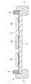
図18の(A)は、半導体チップ100を配置したモールド基板101の断面図である。図18の(B)は、半導体チップ100を配置したモールド基板101の拡大断面図である。図18に示すモールド基板101は、支持基板に半導体チップ100を貼り付けた後、モールド樹脂102を被着して、半導体チップ100及びモールド樹脂102を支持基板から剥離することによって製造されている。図18に示すモールド基板101は、モールド基板101に半導体チップ100を配置している。そのため、半導体チップ100及びモールド樹脂102の線膨張係数に大きな差がある場合、モールド樹脂102の形成の際の昇温に伴う膨張及び降温に伴う収縮により、図18の(B)に示すように、半導体チップ100とモールド樹脂102との界面に隙間が形成される。図18に示すモールド基板101においては、半導体チップ100とモールド樹脂102との界面に深さが5μm以上の隙間が発生してしまう。半導体チップ100とモールド樹脂102との界面に隙間が部分的に集中して形成されると、その後の配線形成プロセスの歩留まりが低くなり、配線の微細加工が困難になるという問題がある。
FIG. 18A is a cross-sectional view of the
半導体チップ100とモールド樹脂102との界面に隙間が部分的に集中して形成されると、例えば、図19に示すように、各半導体チップ100を接続する配線103が形成されなかったり、配線103が細くなったりする場合がある。図19の(A)は、各半導体チップ100を接続する配線103を形成した場合のモールド基板101の平面模式図である。図19の(B)は、図19の(A)のG−G’断面における模式図である。図1
9の(C)は、図19の(A)のH−H’断面における模式図である。半導体チップ100とモールド樹脂102との界面に隙間が部分的に集中して形成されると、配線103の形成に用いられるレジストパターンを形成する際のフォトリソグラフィでデフォーカス(焦点ぼけ)が発生し、レジストパターンが形成されなかったり、レジストパターンが細くなったりする。このようなレジストパターンを用いて、配線103を形成すると、配線103が形成されなかったり、配線103が細くなったりする。
If gaps are formed in a partially concentrated manner at the interface between the
9 (C) is a schematic diagram in the HH ′ cross section of FIG. 19 (A). If gaps are partially concentrated at the interface between the
本件は、半導体装置が有する半導体素子と封止樹脂との界面に形成される隙間を分散する技術を提供する。 The present case provides a technique for dispersing gaps formed at an interface between a semiconductor element included in a semiconductor device and a sealing resin.
本件の一観点による半導体装置は、半導体素子と、前記半導体素子の電極形成面の反対面及び側面を覆う封止樹脂と、を備え、前記半導体素子の電極形成面の外周部分に前記封止樹脂が入り込む導入路が形成されている。 A semiconductor device according to an aspect of the present invention includes a semiconductor element and a sealing resin that covers an opposite surface and a side surface of the electrode formation surface of the semiconductor element, and the sealing resin is disposed on an outer peripheral portion of the electrode formation surface of the semiconductor element. An introduction path into which is inserted is formed.
本件によれば、半導体装置が有する半導体素子と封止樹脂との界面に形成される隙間を分散することができる。 According to this case, it is possible to disperse gaps formed at the interface between the semiconductor element of the semiconductor device and the sealing resin.
以下、図面を参照して、発明を実施するための形態(以下、実施形態という)に係る半導体装置及び半導体装置の製造方法について説明する。 A semiconductor device and a method for manufacturing the semiconductor device according to embodiments for carrying out the invention (hereinafter referred to as embodiments) will be described below with reference to the drawings.
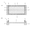
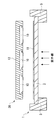
図1の(A)は、本実施形態に係る樹脂封止装置1の平面模式図である。図1の(B)は、図1の(A)のA−A’断面における模式図である。樹脂封止装置1は、複数個の半導体チップ(半導体素子)が載置される載置台2と、載置台2を支持する載置ホルダ3と、載置台2の外周部分に設置された樹脂材型枠4とを、有する。載置台2は、熱膨張係数が小さく、熱プロセスによる変形の小さい材料を用いることが好ましい。載置台2として、例えば、石英基板、シリコンウェーハ、ガラス基板、セラミック基板等を用いてもよい。樹脂材型枠4は、載置台2を囲むように設置されていればよく、例えば、樹脂材型枠4は、立方体形状の部材を組み合わせて載置台2を囲んでいてもよいし、リング状の部材によって載置台2を囲んでいてもよい。樹脂材型枠4の材料は、例えば、ステンレスである。樹脂材型枠4の高さは、任意の値を設定してもよい。樹脂材型枠4の高さに応じて、製造する半導体装置の高さが決まる。例えば、製造する半導体装置の高さを625μmとする場合、樹脂材型枠4の高さを625μmに設定する。
FIG. 1A is a schematic plan view of a
以下、本実施形態に係る半導体装置及び半導体装置の製造方法について、実施例を挙げて説明する。以下の実施例の構成は例示であり、本実施形態は実施例の構成に限定されない。 Hereinafter, the semiconductor device and the method for manufacturing the semiconductor device according to the present embodiment will be described with reference to examples. The configurations of the following examples are illustrative, and the present embodiment is not limited to the configurations of the examples.
まず、図2に示すように、複数の半導体チップ(半導体素子)10を、粘着シート11を介して載置台2に仮固定する。複数の半導体チップ10は、同じ種類であってもよいし、異なる種類であってもよい。図2では、3個の半導体チップ10を載置台2に配置する例を示しているが、半導体チップ10の個数は図2に示す例に限定されず、他の個数であってもよい。また、半導体チップ10は、半導体ウェーハから切り出された後、特性測定の結果、良品と確認された製品を使用してもよい。複数の半導体チップ10の高さ(厚み)は、同じであってもよいし、異なっていてもよい。ここでは、複数の半導体チップ10の高さを同じとしている。
First, as shown in FIG. 2, a plurality of semiconductor chips (semiconductor elements) 10 are temporarily fixed to the mounting table 2 via an
例えば、フリップチップボンダー等のダイボンディング装置を用いて、半導体チップ10の電極形成面(表面)を載置台2に向け、半導体チップ10と載置台2との位置合わせを行い、半導体チップ10を載置台2に配置する。複数の半導体チップ10は、所定間隔で載置台2に配置されている。所定間隔は、例えば、200μm以上500μm以下であるが、所定間隔は、この数値に限定されるものではない。ダイボンディング装置は、アライメント精度が良いものが好ましい。アライメント精度の良いダイボンディング装置を使用することにより、載置台2に配置される各半導体チップ10間の距離を微小にすることができ、各半導体チップ10間の配線をより微細化することができる。各半導体チップ10間を微細配線で接続することができれば、配線数を増やすことができ、小型高密度でより高速の半導体装置を形成することができる。
For example, by using a die bonding apparatus such as a flip chip bonder, the electrode forming surface (front surface) of the
次に、図3に示すように、例えば、スピンコート法又は印刷法により、載置台2の上に配置された複数の半導体チップ10を覆うように、保護材としてのモールド樹脂12を形成する。図3に示すように、半導体チップ10の側面及び半導体チップ10の裏面(半導体チップ10の電極形成面の反対面)が、モールド樹脂12によって覆われている。モールド樹脂12は、例えば、アクリル系樹脂やエポキシ樹脂等の有機系絶縁性樹脂や無機系絶縁性樹脂である。液状樹脂タイプのモールド樹脂12として、例えば、長瀬産業株式会社製のR4212を用いてもよい。顆粒タイプのモールド樹脂12として、例えば、住友ベークライト株式会社製のEME−X83592を用いてもよい。モールド樹脂12は、封止樹脂の一例である。
Next, as shown in FIG. 3, a
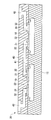
そして、図4に示すように、載置台2の上方に、モールド樹脂12に荷重をかけるための裏面形成金型5を配置する。裏面形成金型5として、例えば、石英基板、シリコンウェーハ、ガラス基板、セラミック基板等を用いてもよい。
Then, as shown in FIG. 4, a back
次いで、図5に示すように、例えば、ラミネータやプレス機等の装置を用いて、モールド樹脂12と裏面形成金型5とを接触させ、裏面形成金型5を載置台2に近づけることにより、モールド樹脂12に対して均一に荷重をかける。この場合、載置台2の外周部分に形成された樹脂材型枠4と裏面形成金型5とが接触するまで、裏面形成金型5を載置台2に近づけることにより、載置台2の上に形成されたモールド樹脂12の厚みが一定になる。この場合、載置台2の上に形成されたモールド樹脂12の厚みが一定となるモールド樹脂12の量を、実験又はシミュレーションによって求めておき、モールド樹脂12の厚みが一定となるモールド樹脂12の量を載置台2の上に形成すればよい。
Next, as shown in FIG. 5, for example, by using an apparatus such as a laminator or a press machine, the
また、例えば、裏面形成金型5の上面に溝を形成しておいてもよい。載置台2の上に形成されたモールド樹脂12の量が少ないと、モールド樹脂12に荷重をかけた際に、モールド樹脂12において気泡の巻き込みが発生する。そのため、モールド樹脂12の量を多めにして載置台2の上に形成し、裏面形成金型5の上面に形成された溝から余剰量のモールド樹脂12を裏面形成金型5の外側に流出させる。これにより、モールド樹脂12における気泡の巻き込みの発生を抑制することができる。また、真空プレス機等を用いて、真空状態下でモールド樹脂12に荷重をかけることにより、モールド樹脂12における気泡の巻き込みの発生をより抑制することができる。
Further, for example, a groove may be formed on the upper surface of the back
なお、モールド樹脂12に荷重をかける際に加熱処理を行うことにより、モールド樹脂12を硬化させる。また、モールド樹脂12の種類によっては、更に紫外線処理を行うことにより、モールド樹脂12を硬化させてもよい。
The
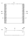
図6に示すように、半導体チップ10の電極形成面には、樹脂導入路21及び樹脂溝22が形成されている。図6の(A)は、実施例1に係る半導体チップ10の平面模式図である。図6の(B)は、図6の(A)のB−B’断面における模式図である。樹脂導入路21は、半導体チップ10の電極形成面の外周部分をハーフダイシングすることによって形成された溝(凹み)である。図6に示すように、樹脂導入路21は、半導体チップ10の側面と接している。樹脂溝22は、半導体チップ10の側面から所定距離を離した位置をハーフダイシングすることによって形成された溝(凹み)である。図6に示すように、樹脂溝22は、半導体チップ10の電極形成面のうちハーフダイシングによって処理されていない部分を囲むように形成された溝である。明細書では、半導体チップ10の電極形成面のうちハーフダイシングによって処理されていない部分を、半導体チップ10の電極形成面の中央部分と表記する。
As shown in FIG. 6, a
図6に示すように、樹脂導入路21及び樹脂溝22は隣接して形成されている。したがって、図6に示すように、半導体チップ10の電極形成面には、樹脂導入路21及び樹脂溝22が、半導体チップ10電極形成面の中央部分から外周部分に向かって樹脂溝22、樹脂導入路21の順で形成されている。すなわち、図6に示すように、半導体チップ10の電極形成面には、半導体チップ10の中央部分を囲むようにして、樹脂導入路21及び樹脂溝22が隣接して形成されている。樹脂溝22の底面は、樹脂導入路21の底面よりも、半導体チップ10の電極形成面から深い位置となっている。樹脂導入路21の深さは、例えば、30μm以上50μm以下である。樹脂導入路21の深さは、半導体チップ10の電極形成面に対して樹脂導入路21を形成する前の半導体チップ10の電極形成面からの距離である。樹脂溝22の深さは、例えば、60μm以上100μm以下である。樹脂溝22の深さは、半導体チップ10の電極形成面に対して樹脂溝22を形成する前の半導体チップ10の電極形成面からの距離である。樹脂導入路21の幅は、例えば、30μm以上50μm以下である。樹脂溝22の幅は、例えば、30μm以上50μm以下である。
As shown in FIG. 6, the
図7は、モールド樹脂12に荷重をかけてモールド樹脂12の厚みを一定にした場合における半導体チップ10の要部断面図である。モールド樹脂12に荷重をかける前は、モールド樹脂12は、半導体チップ10に形成された樹脂導入路21及び樹脂溝22には完全には入り込んでいない。モールド樹脂12に荷重をかけることにより、図7に示すように、モールド樹脂12が、半導体チップ10に形成された樹脂導入路21及び樹脂溝22に入り込み、樹脂導入路21及び樹脂溝22はモールド樹脂12によって満たされる。
FIG. 7 is a cross-sectional view of the main part of the
次に、図8に示すように、モールド樹脂12上の裏面形成金型5を取り外すとともに、載置台2の上の樹脂材型枠4を取り外す。樹脂材型枠4をモールド樹脂12との離型性の良い材料にしたり、樹脂材型枠4に予め離型材を塗布したりしておくことで、載置台2の上の樹脂材型枠4を容易に取り外すことが可能である。
Next, as shown in FIG. 8, the back
そして、図9に示すように、載置台2の裏面から紫外線を照射することにより、粘着シート11の粘着力を弱くした状態で、複数の半導体チップ10及びモールド樹脂12と、載置台2とを分離する。これにより、モールド樹脂12の下面に複数の半導体チップ10が配置され、各半導体チップ10の側面及び裏面がモールド樹脂12によって覆われたモールド基板30が形成される。モールド基板30は、半導体装置の一例である。
And as shown in FIG. 9, in the state which weakened the adhesive force of the
次いで、図10に示すように、半導体チップ10の電極形成面が上になるように、モールド基板30をひっくり返す。図10に拡大して示すように、モールド基板30が有する半導体チップ10の上部には、電極31及びパッシベーション膜32が形成されている。電極31は、例えば、アルミニウム(Al)である。パッシベーション膜32には、電極31の一部を露出する開口が形成されている。パッシベーション膜32は、例えば、酸化シリコン(SiO2)又は窒化シリコン(SiN)等である。
Next, as shown in FIG. 10, the
次に、図11に示すように、モールド基板30の上に、パッシベーション膜40、半導体チップ10同士を接続する配線41、及び、半導体チップ10に形成された電極31と導通する引き出しパッド42を形成する。パッシベーション膜40は、例えば、シリコン窒化膜(Si3N4)及びポリイミド膜の積層膜である。例えば、化学気相堆積(CVD、chemical vapor deposition)法により、シリコン窒化膜(Si3N4)及びポリイミド膜を堆積することにより、パッシベーション膜40を形成する。配線41及び引き出しパッド42は、例えば、アルミニウム(Al)である。例えば、物理気相堆積(PVD、physical vapor deposition)法により、例えば、アルミニウム(Al)を堆積し、フォトリソグラフィ法によりレジストパターンを形成し、レジストパターンをマスクとしてエッチングを行うことによって、配線41及び引き出しパッド42を形成する。
Next, as shown in FIG. 11, the
そして、図12に示すように、パッシベーション膜40、配線41及び引き出しパッド42が形成されたモールド基板30を、ダイシングブレード50によってダイシングすることにより、モールド基板30を分割する。
Then, as shown in FIG. 12, the
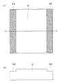
図13の(A)は、モールド基板30の上にパッシベーション膜40及び配線41を形成した場合のモールド基板30の平面模式図である。図13の(B)は、図13の(A)のC−C’断面における模式図である。
FIG. 13A is a schematic plan view of the
モールド樹脂12を硬化させる際の加熱処理によるモールド樹脂12の膨張及びモールド樹脂12の温度が低下した際のモールド樹脂12の収縮によって、半導体チップ10の側面とモールド樹脂12との界面に隙間が発生する。半導体チップ10の電極形成面には、樹脂導入路21及び樹脂溝22が形成されており、モールド樹脂12が、半導体チップ10の電極形成面に形成された樹脂導入路21及び樹脂溝22に入り込んでいる。したがって、モールド樹脂12の収縮が、半導体チップ10の側面とモールド樹脂12との界面に集中することが抑制される。すなわち、モールド樹脂12の収縮が、半導体チップ10の側面、半導体チップ10の電極形成面に形成された樹脂導入路21及び樹脂溝22で発生することにより、モールド樹脂12の収縮の発生が分散される。その結果、半導体チップ10の側面とモールド樹脂12との界面における隙間が分散され、半導体チップ10の側面とモールド樹脂12との界面に隙間が部分的に集中して形成されることが抑制される。
A gap is generated at the interface between the side surface of the
また、半導体チップ10の電極形成面に形成された樹脂導入路21及び樹脂溝22に入り込んだモールド樹脂12は鉤状になる。鉤状になったモールド樹脂12の先端が樹脂導入路21に引っかかることにより、モールド樹脂12の収縮が抑制され、半導体チップ10の側面とモールド樹脂12との界面における隙間が減少する。
Further, the
実施例1に係る半導体装置によれば、半導体チップ10の側面とモールド樹脂12との界面に発生する隙間の深さを1μm未満にすることが可能となる。半導体チップ10の側面とモールド樹脂12との界面における隙間が分散及び減少することにより、半導体チップ10の上に形成されるパッシベーション膜40の凹みが浅くなる。半導体チップ10の上に形成されるパッシベーション膜40の凹みが浅くなると、パッシベーション膜40の上に堆積されるアルミニウム(Al)の凹みも浅くなる。これにより、フォトリソグラフィ法によって、配線41を形成するためのレジストパターンを露光する際のデフォーカス(焦点ぼけ)が抑制される。したがって、レジストパターンが形成されなかったり、レジストパターンが細くなったりすることが抑制される。この結果、レジストパターンをマスクとしてエッチングした場合において、配線41が形成されなかったり、配線41が細くなったりすることが抑制される。
According to the semiconductor device according to the first embodiment, the depth of the gap generated at the interface between the side surface of the
一方、半導体チップ10の側面とモールド樹脂12との界面における隙間が深いと、半導体チップ10の上に形成されるパッシベーション膜40の凹みが深くなる。半導体チップ10の上に形成されるパッシベーション膜40の凹みが深くなると、パッシベーション膜40の上に堆積されるアルミニウム(Al)の凹みも深くなる。パッシベーション膜40の上に堆積されるアルミニウム(Al)の凹みが深いと、配線41を形成するためのレジストパターンを露光する際のデフォーカス(焦点ぼけ)によりレジストパターンが形成されなかったり、レジストパターンが細くなったりする。その結果、配線41が形成されなかったり、配線41が細くなったりする。
On the other hand, when the gap at the interface between the side surface of the
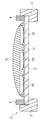
上記では、複数の半導体チップ10の高さを同じにした場合の例を示した。複数の半導体チップ10の高さが異なる場合の例を図14に示す。図14においては、半導体チップ10Aの高さと、半導体チップ10Bの高さとが異なっている。半導体チップ10Aの高さは、例えば、300μmであり、半導体チップ10Bの高さは、例えば、200μmである。
In the above, an example in which the heights of the plurality of
半導体チップ10Bの高さは、半導体チップ10Aの高さよりも低いので、半導体チップ10Bの裏面側に形成されているモールド樹脂12の量が、半導体チップ10Aの裏面側に形成されているモールド樹脂12の量よりも多い。半導体チップ10Bの高さが半導体チップ10Aの高さよりも低い場合、半導体チップ10Aの高さと半導体チップ10Bの高さが同じ場合と比較して、半導体チップ10Aと半導体チップ10Bとの間に存在するモールド樹脂12は、半導体チップ10Bの裏面側に引っ張られる。そのため、半導体チップ10Bの高さが半導体チップ10Aの高さよりも低い場合、半導体チップ10Aの高さと半導体チップ10Bの高さが同じ場合と比較して、半導体チップ10Aの側面とモールド樹脂12との界面における隙間は大きくなる。
Since the height of the
半導体チップ10の電極形成面に樹脂導入路21及び樹脂溝22が形成されていない場合、隣接する半導体チップ10の高さが異なっていると、隣接する半導体チップ10の高さが同じ場合と比較して、高さが高い方の半導体チップ10の側面とモールド樹脂12との界面における隙間は大きくなる。実施例1に係る半導体装置においては、半導体チップ10の電極形成面に樹脂導入路21及び樹脂溝22が形成されている。そのため、隣接する半導体チップ10の高さが異なっていても、半導体チップ10の側面とモールド樹脂12との界面における隙間が分散されるとともに、半導体チップ10の側面とモールド樹脂12との界面における隙間が減少する。
When the
実施例2に係る半導体装置について説明する。実施例2では、半導体チップ10の電極形成面に樹脂導入路61を形成し、半導体チップ10の電極形成面に樹脂溝22を形成しない点が、実施例1と異なっており、他の点については実施例1と同様である。なお、実施例1と同一の構成要素については、実施例1と同一の符号を付し、その説明を省略する。
A semiconductor device according to Example 2 will be described. The second embodiment is different from the first embodiment in that the
図15の(A)は、実施例2に係る半導体チップ10の平面模式図であり、図15の(B)は、図15の(A)のD−D’断面における模式図である。図15に示すように、半導体チップ10の電極形成面には、樹脂導入路61が形成されている。樹脂導入路61は、半導体チップ10の電極形成面の外周部分をハーフダイシングすることによって形成された溝(凹み)であり、図15に示すように、樹脂導入路61は、半導体チップ10の側面と接している。図15に示すように、樹脂導入路61は、半導体チップ10の電極形成面のうちハーフダイシングによって処理されていない部分を囲むように形成された溝である。樹脂導入路61の深さは、例えば、30μm以上50μm以下である。樹脂導入路61の深さは、半導体チップ10の電極形成面に対して樹脂導入路61を形成する前の半導体チップ10の電極形成面からの距離である。樹脂導入路61の幅は、例えば、90μm以上150μm以下である。
FIG. 15A is a schematic plan view of the
モールド樹脂12を硬化させる際の加熱処理によるモールド樹脂12の膨張及びモールド樹脂12の温度が低下した際のモールド樹脂12の収縮によって、半導体チップ10の側面とモールド樹脂12との界面に隙間が発生する。半導体チップ10の電極形成面には、樹脂導入路61が形成されており、モールド樹脂12が、半導体チップ10の電極形成面に形成された樹脂導入路61に入り込む。したがって、モールド樹脂12の収縮が、半導体チップ10の側面とモールド樹脂12との界面に部分的に集中することが抑制される。すなわち、モールド樹脂12の収縮が、半導体チップ10の側面及び半導体チップ10の電極形成面に形成された樹脂導入路61で発生することにより、モールド樹脂12の収縮の発生が分散される。その結果、半導体チップ10の側面とモールド樹脂12との界面における隙間が分散され、半導体チップ10の側面とモールド樹脂12との界面に隙間が部分的に集中して形成されることが抑制される。
A gap is generated at the interface between the side surface of the
実施例2に係る半導体装置によれば、半導体チップ10の側面とモールド樹脂12との界面に発生する隙間の深さを1μm未満にすることが可能となる。半導体チップ10の側面とモールド樹脂12との界面における隙間が分散することにより、半導体チップ10の上に形成されるパッシベーション膜40の凹みが浅くなる。半導体チップ10の上に形成されるパッシベーション膜40の凹みが浅くなると、パッシベーション膜40の上に堆積されるアルミニウム(Al)の凹みも浅くなる。これにより、フォトリソグラフィ法によって、配線41を形成するためのレジストパターンを露光する際のデフォーカス(焦点ぼけ)が抑制される。したがって、レジストパターンが形成されなかったり、レジストパターンが細くなったりすることが抑制される。この結果、レジストパターンをマスクとしてエッチングした場合において、配線41が形成されなかったり、配線41が細くなったりすることが抑制される。
According to the semiconductor device according to the second embodiment, it is possible to make the depth of the gap generated at the interface between the side surface of the
〈変形例〉
実施例1では、樹脂導入路21を半導体チップ10の電極面の外周部分に形成し、樹脂溝22を半導体チップ10の電極面の中央部分と樹脂導入路21との間に形成する例を示した。本実施形態は、これに限定されず、樹脂導入路21及び樹脂溝22の形成位置を、図16に示す半導体チップ10のように変更してもよい。図16の(A)は、実施例1の変形例に係る半導体チップ10の平面模式図であり、図16の(B)は、図16の(A)のE−E’断面における模式図である。図16に示すように、樹脂導入路21Aと、樹脂導入路21Bとが対向するように、樹脂導入路21A及び21Bを半導体チップ10の電極面の外周部分に形成してもよい。図16に示すように、樹脂溝22Aと樹脂溝22Bとが対向するように、樹脂溝22Aを半導体チップ10の電極面の中央部分と樹脂導入路21Aとの間に形成し、樹脂溝22Bを半導体チップ10の電極面の中央部分と樹脂導入路21Bとの間に形成してもよい。
<Modification>
In the first embodiment, an example in which the
半導体チップ10の電極面に樹脂導入路21A及び樹脂溝22Aを形成し、半導体チップ10の電極面に樹脂導入路21B及び樹脂溝22Bを形成しないようにしてもよい。すなわち、半導体チップ10の電極面の外周部分の四辺のうちのいずれか一辺に樹脂導入路21Aを形成し、半導体チップ10の電極面の中央部分と樹脂導入路21Aとの間に樹脂溝22Aを形成するようにしてもよい。また、半導体チップ10の電極面の外周部分の四辺のうちのいずれか三辺に樹脂導入路21を形成し、半導体チップ10の電極面の中央部分と樹脂導入路21との間に樹脂溝22を形成するようにしてもよい。
The
実施例2では、樹脂導入路61を半導体チップ10の電極面の外周部分に形成する例を示した。本実施形態は、これに限定されず、樹脂導入路61の形成位置を、図17に示す半導体チップ10のように変更してもよい。図17の(A)は、実施例2の変形例に係る半導体チップ10の平面模式図であり、図17の(B)は、図17の(A)のF−F’断面における模式図である。図17に示すように、樹脂導入路61Aと、樹脂導入路61Bとが対向するように、樹脂導入路61A及び61Bを半導体チップ10の電極面の外周部分に形成してもよい。
In the second embodiment, an example in which the
半導体チップ10の電極面に樹脂導入路61Aを形成し、半導体チップ10の電極面に樹脂導入路61Bを形成しないようにしてもよい。すなわち、半導体チップ10の電極面の外周部分の四辺のうちのいずれか一辺に樹脂導入路61Aを形成するようにしてもよい
。また、半導体チップ10の電極面の外周部分の四辺のうちのいずれか三辺に樹脂導入路61を形成するようにしてもよい。
The
1 樹脂封止装置
2 載置台
3 載置ホルダ
4 樹脂材型枠
5 裏面形成金型
10 半導体チップ
11 粘着シート
12 モールド樹脂
21、21A、21B、61、61A、61B 樹脂導入路
22、22A、22B 樹脂溝
30 モールド基板
31 電極
32、40 パッシベーション膜
41 配線
42 引き出しパッド
50 ダイシングブレード
DESCRIPTION OF
Claims (3)
前記半導体素子の電極形成面の反対面及び側面を覆う封止樹脂と、を備え、
前記半導体素子の電極形成面の外周部分に前記封止樹脂が入り込む導入路が形成されていることを特徴とする半導体装置。 A semiconductor element;
A sealing resin covering the opposite surface and side surface of the electrode formation surface of the semiconductor element,
An introduction path into which the sealing resin enters is formed in an outer peripheral portion of an electrode formation surface of the semiconductor element.
前記溝の底面は、前記導入路の底面よりも前記電極形成面から深い位置であることを特徴とする請求項1に記載の半導体装置。 A groove into which the sealing resin enters is formed between the central portion of the electrode formation surface of the semiconductor element and the introduction path,
The semiconductor device according to claim 1, wherein a bottom surface of the groove is deeper than the electrode formation surface than a bottom surface of the introduction path.
一方の前記半導体素子の高さと、他方の前記半導体素子の高さとが異なることを特徴とする請求項1又は2に記載の半導体装置。 Comprising a plurality of the semiconductor elements;
3. The semiconductor device according to claim 1, wherein a height of one of the semiconductor elements is different from a height of the other semiconductor element.
Priority Applications (1)
| Application Number | Priority Date | Filing Date | Title |
|---|---|---|---|
| JP2011063066A JP2012199420A (en) | 2011-03-22 | 2011-03-22 | Semiconductor device |
Applications Claiming Priority (1)
| Application Number | Priority Date | Filing Date | Title |
|---|---|---|---|
| JP2011063066A JP2012199420A (en) | 2011-03-22 | 2011-03-22 | Semiconductor device |
Publications (1)
| Publication Number | Publication Date |
|---|---|
| JP2012199420A true JP2012199420A (en) | 2012-10-18 |
Family
ID=47181346
Family Applications (1)
| Application Number | Title | Priority Date | Filing Date |
|---|---|---|---|
| JP2011063066A Pending JP2012199420A (en) | 2011-03-22 | 2011-03-22 | Semiconductor device |
Country Status (1)
| Country | Link |
|---|---|
| JP (1) | JP2012199420A (en) |
Cited By (1)
| Publication number | Priority date | Publication date | Assignee | Title |
|---|---|---|---|---|
| JP2017504194A (en) * | 2013-12-19 | 2017-02-02 | ザ リージェンツ オブ ザ ユニバーシティ オブ カリフォルニア | Highly scalable manufacturing technology and packaging devices for electronic circuits |
Citations (5)
| Publication number | Priority date | Publication date | Assignee | Title |
|---|---|---|---|---|
| JP2000252239A (en) * | 1999-02-26 | 2000-09-14 | Omron Corp | Semiconductor electronic component and manufacture thereof |
| US20020167078A1 (en) * | 2001-02-20 | 2002-11-14 | Johann Winderl | Electronic component with a semiconductor chip and method of producing an electronic component |
| JP2004056093A (en) * | 2002-05-31 | 2004-02-19 | Fujitsu Ltd | Semiconductor device and method of manufacturing the semiconductor device |
| US20080009102A1 (en) * | 2006-07-07 | 2008-01-10 | Advanced Semiconductor Engineering Inc. | Method for Encasulating Sensor Chips |
| US7508083B2 (en) * | 2003-03-11 | 2009-03-24 | Infineon Technologies Ag | Electronic component comprising a semiconductor chip and a plastic housing, and method for producing the same |
-
2011
- 2011-03-22 JP JP2011063066A patent/JP2012199420A/en active Pending
Patent Citations (5)
| Publication number | Priority date | Publication date | Assignee | Title |
|---|---|---|---|---|
| JP2000252239A (en) * | 1999-02-26 | 2000-09-14 | Omron Corp | Semiconductor electronic component and manufacture thereof |
| US20020167078A1 (en) * | 2001-02-20 | 2002-11-14 | Johann Winderl | Electronic component with a semiconductor chip and method of producing an electronic component |
| JP2004056093A (en) * | 2002-05-31 | 2004-02-19 | Fujitsu Ltd | Semiconductor device and method of manufacturing the semiconductor device |
| US7508083B2 (en) * | 2003-03-11 | 2009-03-24 | Infineon Technologies Ag | Electronic component comprising a semiconductor chip and a plastic housing, and method for producing the same |
| US20080009102A1 (en) * | 2006-07-07 | 2008-01-10 | Advanced Semiconductor Engineering Inc. | Method for Encasulating Sensor Chips |
Cited By (1)
| Publication number | Priority date | Publication date | Assignee | Title |
|---|---|---|---|---|
| JP2017504194A (en) * | 2013-12-19 | 2017-02-02 | ザ リージェンツ オブ ザ ユニバーシティ オブ カリフォルニア | Highly scalable manufacturing technology and packaging devices for electronic circuits |
Similar Documents
| Publication | Publication Date | Title |
|---|---|---|
| KR100903472B1 (en) | Method of separating semiconductor dies from a wafer | |
| US9337097B2 (en) | Chip package and method for forming the same | |
| US20080191335A1 (en) | Cmos image sensor chip scale package with die receiving opening and method of the same | |
| US9165890B2 (en) | Chip package comprising alignment mark and method for forming the same | |
| JP2008160084A (en) | Wafer level package with die storing cavity and its method | |
| JP2008252087A (en) | Structure of semiconductor device package and method of the same | |
| US20170148761A1 (en) | Method of fabricating semiconductor package | |
| TWI529887B (en) | Chip package and method for forming the same | |
| JP2008244437A (en) | Image sensor package having die receiving opening and method thereof | |
| KR20080075450A (en) | Wafer level image sensor package with die receiving cavity and method of the same | |
| US8810012B2 (en) | Chip package, method for forming the same, and package wafer | |
| KR20190038253A (en) | Info-pop structures with tivs having cavities | |
| US9024437B2 (en) | Chip package and method for forming the same | |
| JP6933697B2 (en) | Chip package and its manufacturing method | |
| JP2012160734A (en) | Interposer and method for forming the same | |
| US20180374717A1 (en) | Semiconductor package and method of forming the same | |
| JP2012216601A (en) | Electronic device manufacturing method and electronic device | |
| US20090102056A1 (en) | Patterned Leads For WLCSP And Method For Fabricating The Same | |
| JP2005064473A (en) | Semiconductor device and manufacturing method for the same | |
| JP2012199420A (en) | Semiconductor device | |
| JP2008288481A (en) | Semiconductor device and method for manufacturing the same | |
| TWI680546B (en) | Packaged semiconductor device and method for preparing the same | |
| KR102202634B1 (en) | Semiconductor package and semiconductor module including the same | |
| JP2013187434A (en) | Semiconductor device, method for manufacturing the same, electronic equipment, and substrate | |
| KR20090127742A (en) | Wafer level chip scale package and fabricating method of the same |
Legal Events
| Date | Code | Title | Description |
|---|---|---|---|
| A621 | Written request for application examination |
Free format text: JAPANESE INTERMEDIATE CODE: A621 Effective date: 20140108 |
|
| A977 | Report on retrieval |
Free format text: JAPANESE INTERMEDIATE CODE: A971007 Effective date: 20140807 |
|
| A131 | Notification of reasons for refusal |
Free format text: JAPANESE INTERMEDIATE CODE: A131 Effective date: 20140819 |
|
| A521 | Written amendment |
Free format text: JAPANESE INTERMEDIATE CODE: A523 Effective date: 20141016 |
|
| A131 | Notification of reasons for refusal |
Free format text: JAPANESE INTERMEDIATE CODE: A131 Effective date: 20150310 |
|
| A02 | Decision of refusal |
Free format text: JAPANESE INTERMEDIATE CODE: A02 Effective date: 20150915 |