JP2012164792A - Via structure and manufacturing method thereof - Google Patents
Via structure and manufacturing method thereof Download PDFInfo
- Publication number
- JP2012164792A JP2012164792A JP2011023684A JP2011023684A JP2012164792A JP 2012164792 A JP2012164792 A JP 2012164792A JP 2011023684 A JP2011023684 A JP 2011023684A JP 2011023684 A JP2011023684 A JP 2011023684A JP 2012164792 A JP2012164792 A JP 2012164792A
- Authority
- JP
- Japan
- Prior art keywords
- hole
- substrate
- wiring
- via structure
- forming
- Prior art date
- Legal status (The legal status is an assumption and is not a legal conclusion. Google has not performed a legal analysis and makes no representation as to the accuracy of the status listed.)
- Pending
Links
Images


Abstract
Description
本発明は、集積回路などが形成される基板を貫通するヴィア構造およびその作製方法 The present invention relates to a via structure penetrating a substrate on which an integrated circuit or the like is formed, and a method for manufacturing the via structure.
化合物半導体を用いた集積回路(IC)の高周波化が進展するに従い、高周波信号のチップ内共振周波数が低下するため、チップ内共振は、高周波設計上大きな問題となっている。チップ内共振を抑制するため、近年では、基板を貫通するヴィアを形成して基板裏面のグランドとチップ表面とを接続し、チップのグランドを強化することが極めて重要になってきている。 As the frequency of integrated circuits (ICs) using compound semiconductors increases, the in-chip resonance frequency of high-frequency signals decreases, and thus in-chip resonance is a major problem in high-frequency design. In order to suppress intra-chip resonance, in recent years, it has become extremely important to form vias penetrating the substrate and connect the ground on the back surface of the substrate and the chip surface to strengthen the ground of the chip.
基板を貫通するヴィア(基板貫通ヴィア)の形成においては、回路形成面(基板表面)のプロセスが完了した後、裏面よりヴィアの形成プロセスを行う「ヴィアラスト方式」が主流である。この方式によれば、回路形成面の凹凸を最小限に抑え、高い歩留まりを維持しながら基板貫通ヴィアを形成することができる。 In the formation of vias penetrating the substrate (through-substrate vias), the “via last method”, in which the via formation process is performed from the back surface after the process of the circuit formation surface (substrate surface) is completed, is the mainstream. According to this method, through-substrate vias can be formed while minimizing irregularities on the circuit formation surface and maintaining a high yield.
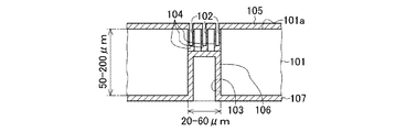
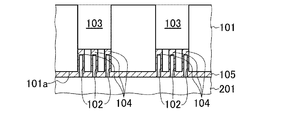
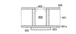
ヴィアラスト方式では、図8に示すように、まず、基板801表面の回路形成面801aに、表面配線層802を含む所望とする回路を形成した後、ヴィア形成箇所にランドメタル層803を形成する。この後、基板801の裏面側より基板貫通ヴィア804をエッチング形成する。この形成時に、既に形成してあるランドメタル層803が、エッチング停止層として機能する。この後、基板貫通ヴィア804内に、表面配線層802に接続する貫通配線層805を形成し、また、貫通配線層805に接続する裏面配線層806を形成する。
In the via last method, as shown in FIG. 8, first, a desired circuit including the
このような基板貫通ヴィアの形成技術として、例えば、シリコン基板を用いた集積回路では、ボッシュプロセスと呼ばれるエッチングとエッチング側壁保護とを繰り返すヴィア形成方法がある。この技術によれば、微細な径の基板貫通ヴィアが形成可能とされている。 As a technique for forming such a through-substrate via, for example, in an integrated circuit using a silicon substrate, there is a via formation method that repeats etching and etching sidewall protection called a Bosch process. According to this technique, a through-substrate via having a fine diameter can be formed.
一方、化合物半導体などのシリコン以外の材料による基板の場合、上述したボッシュプロセスを用いることができず、例えば、InP基板の場合、ヨウ化水素ガスを用いたドライエッチングで基板貫通ヴィアを形成している(非特許文献1参照)。また、窒化物化合物半導体,SiC,およびサファイアなどの基板の場合、金属マスクを用いたドライエッチングに出基板貫通ヴィアを形成している(特許文献1参照)。 On the other hand, in the case of a substrate made of a material other than silicon such as a compound semiconductor, the above-described Bosch process cannot be used. For example, in the case of an InP substrate, a through-substrate via is formed by dry etching using hydrogen iodide gas. (See Non-Patent Document 1). In the case of a substrate such as a nitride compound semiconductor, SiC, and sapphire, a through-substrate through-via is formed by dry etching using a metal mask (see Patent Document 1).
しかしながら、上述した基板貫通ヴィアの形成技術では、次に示すような問題がある。 However, the above-described through-substrate via formation technique has the following problems.
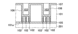
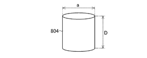
シリコン以外の基板における基板貫通ヴィアの形成では、いわゆるボッシュプロセスが適用できないため、長時間のドライエッチングで基板貫通ヴィアを形成することになる。このため、第1に、ドライエッチングが長くなることによってヴィアのサイドエッチングや残渣の発生が顕著となり、ヴィアの径を拡大する必要が生じ、微細な径のヴィアを形成することが困難であった。例えば、図9の斜視図に示すように、基板貫通ヴィア804の深さDが50〜200μmの場合、孔径aは、80μm程度となる。このように基板貫通ヴィアの孔径が大きくなると、ランドメタル層を大面積に形成することになり、回路形成面における回路形成領域の減少を招き、チップの大型化、集積度の低下などの問題を招くことになる。
In the formation of through-substrate vias on a substrate other than silicon, a so-called Bosch process cannot be applied, and thus through-substrate vias are formed by long-time dry etching. For this reason, firstly, the longer side of dry etching, the side etching of vias and the generation of residue become remarkable, and it is necessary to enlarge the diameter of the via, and it is difficult to form a via having a fine diameter. . For example, as shown in the perspective view of FIG. 9, when the depth D of the substrate through
第2に、長いドライエッチング処理が必要となるため、基板貫通ヴィア形成用のエッチングマスク耐性の要求条件が厳しくなるといった問題がある。このため、エッチングマスク材料の制限、およびドライエッチング条件自体に制限が生じるようになる。 Secondly, since a long dry etching process is required, there is a problem that requirements for etching mask resistance for forming through-substrate vias become severe. For this reason, there are restrictions on the etching mask material and the dry etching conditions themselves.
第3に、基板貫通ヴィアの大型化に伴ってランドメタル層の基板側に大きな空間が存在するようになる。このため、自身の応力でランドメタル層に反りが発生し、集積回路チップの信頼性を大幅に低下させてしまうという問題が生じていた。ランドメタル層の反りを回避するには、ランドメタル層をより厚く形成することになる。しかしながら、このために、ランドメタル層用のプロセスが別途必要になり、また、表面多層配線を重畳するなど、プロセスの増加が生じ、結果としてスループットの低下、および配線レイアウトの制限などが生じてしまっていた。 Thirdly, a large space exists on the substrate side of the land metal layer as the size of the through-via via increases. Therefore, the land metal layer is warped by its own stress, and the reliability of the integrated circuit chip is greatly lowered. In order to avoid warping of the land metal layer, the land metal layer is formed thicker. However, this requires a separate process for the land metal layer, and increases the number of processes such as superimposing surface multilayer wiring, resulting in a decrease in throughput and a limitation on wiring layout. It was.
本発明は、以上のような問題点を解消するためになされたものであり、より小さな径の基板貫通ヴィアが形成できるようにすることを目的とする。 The present invention has been made to solve the above-described problems, and an object of the present invention is to enable formation of a substrate through via having a smaller diameter.
本発明に係るヴィア構造は、基板の回路が形成されている主表面側から所望の孔径の範囲で形成可能な深さに形成された第1孔部と、基板の裏面側から形成されて第1孔部に接続する第2孔部と、第1孔部の内部に形成された第1孔部配線と、第1孔部配線に接続して基板の主表面側に形成された表面配線層と、第2孔部の内部に第1孔部配線に接続して形成された第2孔部配線と、第2孔部配線に接続して基板の裏面側に形成された裏面配線層とを少なくとも備える。 The via structure according to the present invention is formed from the first hole portion formed at a depth that can be formed within a desired hole diameter range from the main surface side where the circuit of the substrate is formed, and the back surface side of the substrate. A second hole connected to the first hole, a first hole wiring formed in the first hole, and a surface wiring layer formed on the main surface side of the substrate connected to the first hole wiring A second hole wiring formed inside the second hole connected to the first hole wiring, and a back wiring layer formed on the back side of the substrate connected to the second hole wiring. At least.
上記のヴィア構造において、第1孔部に接触する表面配線層で構成されたランドメタル層を備えるようにしてもよい。なお、第1孔部の孔径は、2〜20μmであればよい。 The via structure may include a land metal layer composed of a surface wiring layer in contact with the first hole. In addition, the hole diameter of a 1st hole part should just be 2-20 micrometers.
本発明に係るヴィア構造の作製方法は、基板の回路が形成される主表面側から所望の孔径の範囲で形成可能な深さに第1孔部を形成する第1工程と、第1孔部の内部に第1孔部配線を形成する第2工程と、基板の主表面側に第1孔部配線に接続する表面配線層を形成する第3工程と、基板の裏面側から第1孔部に接続する第2孔部を形成する第4工程と、第2孔部の内部に第1孔部配線に接続する第2孔部配線を形成する第5工程と、基板の裏面側に第2孔部配線に接続する裏面配線層を形成する第6工程とを少なくとも備える。 The via structure manufacturing method according to the present invention includes a first step of forming a first hole at a depth that can be formed in a range of a desired hole diameter from a main surface side on which a circuit of a substrate is formed, and a first hole The second step of forming the first hole wiring inside the substrate, the third step of forming the surface wiring layer connected to the first hole wiring on the main surface side of the substrate, and the first hole portion from the back side of the substrate A fourth step of forming a second hole connected to the second hole, a fifth step of forming a second hole wiring connected to the first hole wiring inside the second hole, and a second step on the back side of the substrate. And a sixth step of forming a back surface wiring layer connected to the hole wiring.
上記ヴィア構造の作製方法において、第1工程では、第1孔部とともに素子間分離のための溝部を形成してもよい。また、第1工程では、第1孔部とともにキャパシタを構成する溝部を形成してもよい。 In the via structure manufacturing method, in the first step, a groove for element isolation may be formed together with the first hole. Further, in the first step, a groove part constituting the capacitor may be formed together with the first hole part.
以上説明したように、本発明によれば、基板の裏面側から形成されて第1孔部に接続する第2孔部を設けるようにしたので、より小さな径の基板貫通ヴィアが形成できるようになるという優れた効果が得られる。 As described above, according to the present invention, since the second hole portion formed from the back surface side of the substrate and connected to the first hole portion is provided, a substrate through via having a smaller diameter can be formed. An excellent effect is obtained.
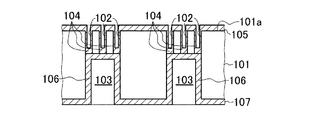
以下、本発明の実施の形態について図を参照して説明する。図1は、本発明の実施の形態におけるヴィア構造の構成を示す構成図である。図1では、ヴィア構造の断面を概略的に示している。 Hereinafter, embodiments of the present invention will be described with reference to the drawings. FIG. 1 is a configuration diagram showing the configuration of the via structure in the embodiment of the present invention. FIG. 1 schematically shows a cross section of the via structure.
このヴィア構造は、まず、基板101の回路が形成される主表面101a側から所望の孔径の範囲で形成可能な深さに形成された第1孔部102と、基板101の裏面側から形成されて第1孔部102に接続する第2孔部103とを備える。
This via structure is first formed from the
また、このヴィア構造は、第1孔部102の内部に形成された第1孔部配線104と、第1孔部配線104に接続して基板101の主表面101a側に形成された表面配線層105と、第2孔部103の内部に第1孔部配線104に接続して形成された第2孔部配線106と、第2孔部配線106に接続して基板101の裏面側に形成された裏面配線層107とを備える。
In addition, this via structure includes a
ここで、基板101は、例えば、InP、GaAs、GaNなど化合物半導体から構成されたものであればよい。これらの基板の場合、典型的な基板厚は、50〜200μmである。この程度の厚さの基板であれば、孔部(ヴィア)形成などの各プロセスにおける基板のハンドリング性を良好な状態とすることができる。なお、第1孔部102と第2孔部103よりなるヴィアにおける接地強化効果、および電気伝導や信号伝播特性を良好に維持することができる構造であれば、いかなる基板厚さでも構わない。
Here, the
上述した本実施の形態におけるヴィア構造によれば、所望の孔径の範囲で形成可能な深さに第1孔部102を形成してあるので、裏面から形成する第2孔部103は、基板101を貫通して形成することなく、基板101の途中までエッチングすることで形成すればよい。このため、第2孔部103の形成では、エッチング量が減少し、また、エッチング残渣を減少させることができるので、孔径を拡大する必要がなく、微細な孔径に形成することができる。
According to the via structure in the present embodiment described above, the
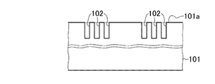
例えば、第1孔部102は、孔径2〜20μm程度とし、深さは5〜20μmとすることができる。この場合、例えば、基板101の板厚が50〜200μmであれば、第2孔部103の深さは、45〜180μm程度とし、孔径は20〜60μm程度とすることができる。ここで、図2の斜視図に示すように、円柱形状とした第1孔部202の直径cとし、第2孔部203の直径をbとし、図9に示した従来の基板貫通ヴィア804の直径をaとすると、a>b>cとすることができる。なお、図2では、各孔部を円筒形状としているが、これに限るものではなく、図3の斜視図に示すように、第1孔部302および第2孔部303の形状を、角柱およびその他の形状としてもよい。
For example, the
なお、第1孔部配線104および第2孔部配線106は、例えば、Au,Cu,Al,Wなどの金属から構成すればよい。例えば、第1孔部配線104は、厚さ0.5〜3μmとし、第1孔部102の孔内の表面を被覆するように形成すればよい。一方、第2孔部配線106は、厚さ3〜20μmとし、第2孔部103の孔内の表面を被覆するように形成すればよい。また、孔内を金属で充填して貫通配線としてもよい。
Note that the
また、本実施の形態によれば、エッチング量を減らすことができるので、エッチングに用いる利用可能なマスク材料の選択肢が増え、また、エッチング種やエッチング温度などのエッチング条件の設計自由度も飛躍的に向上する。 In addition, according to the present embodiment, the amount of etching can be reduced, so there are more choices of mask materials that can be used for etching, and the design flexibility of etching conditions such as etching species and etching temperature is dramatically increased. To improve.
また、第1孔部102の側にランドメタル層を形成する場合、ランドメタル層の基板側に大きな空間が形成されることがなくなるので、ランドメタル層における反りの問題が解消できるようになり、ランドメタル層をより薄く形成することが可能となる。
In addition, when the land metal layer is formed on the
次に、本実施の形態におけるヴィア構造の作製方法について、図4A〜図4Hを用いて説明する。図4A〜図4Hは、本発明の実施の形態におけるヴィア構造の作製途中の状態を示す断面図である。 Next, a method for manufacturing the via structure in this embodiment will be described with reference to FIGS. 4A to 4H are cross-sectional views showing a state in the middle of manufacturing the via structure in the embodiment of the present invention.
まず、図4Aに示すように、基板101を用意する。基板101は、例えばInP基板、GaAs基板、GaN基板などである。
First, as shown in FIG. 4A, a
次に、図4Bに示すように、回路が形成されている主表面101aの側から、所望の孔径の範囲で形成可能な深さに第1孔部102を形成する。例えば、直径2〜20μmで深さ5〜20μmの円筒形状の第1孔部102を形成する。例えば、Cl2,HBr,HIなどのハロゲン系ガスを用いたドライエッチングにより、第1孔部102を形成すればよい。形成した孔部の側壁が滑らかで微細な孔径に形成可能であれば、いかなるガス種を用いても構わない。また、ウェットエッチングが可能なエッチャントによって第1孔部102を形成してもよい。
Next, as shown in FIG. 4B, the
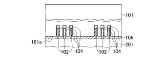
次に、図4Cに示すように、第1孔部102の内部に第1孔部配線104を形成し、また、基板101の主表面101a側に第1孔部配線104に接続する表面配線層105を形成する。例えば、Au,Cu,Al,Wなどの金属を、例えば、真空蒸着法,スパッタリング法,およびメッキ法などにより堆積することで、第1孔部配線104および表面配線層105を形成すればよい。図4Cでは、第1孔部102の壁面を覆うように第1孔部配線104を形成した状態を示しているが、第1孔部配線104は、第1孔部102の内部を金属で充填して形成してもよい。
Next, as shown in FIG. 4C, the
次に、図4Dに示すように、基板101の主表面101a側に、サポート基板201を貼り付ける。サポート基板201は、例えばガラスから構成すればよい。また、サポート基板201は、例えば、UVで接着剤硬化する接着剤および熱で接着剤硬化する接着剤などにより接着すればよい。サポート基板201を貼り付けることで、基板101の主表面101aの側を保護した状態で、基板101の裏面側の様々な処理が行えるようになる。
Next, as shown in FIG. 4D, a
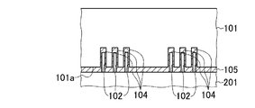
次に、図4Eに示すように、基板101を薄層化する。例えば、基板101の裏面側を、砥石による研磨装置とCMP(Chemical Mechanical Polishing)により研削研磨することで、基板101を薄層化することができる。例えば、基板厚が、50〜200μmとなるように薄層化する。なお、基板101が薄いほど裏面から孔部を形成するときのエッチング時間が短くなるため有利であるが、50μmより薄いと、基板のハンドリング性は下がる。このため、基板厚は、50〜200μmとした方がよい。ただし、基板の良好なハンドリング性が確保されれば、基板厚を50μm以下としても構わない。また、良好なドライエッチング条件による深堀エッチングが実現できるのであれば、基板厚は200μm以上としてもよい。
Next, as shown in FIG. 4E, the
次に、図4Fに示すように、基板101の裏面側から第1孔部102に接続する第2孔部103を形成する。例えば、ドライエッチングにより、深さ20〜60μmに第2孔部103を形成すればよい。基板表面までドライエッチングする従来の方法よりも、短いドライエッチング時間で、第2孔部103が形成できるので、サイドエッチングや残渣が少なく、側壁が滑らかで微細な孔径にすることが可能となる。ここで、形成した孔部の側壁が滑らかで微細な孔径に形成可能であれば、いかなるガス種を用いても構わない。また、ウェットエッチングが可能なエッチャントによって第1孔部102を形成してもよい。
Next, as shown in FIG. 4F, a
次に、図4Gに示すように、第2孔部103の内部に第1孔部配線104に接続する第2孔部配線106を形成し、基板101の裏面側に第2孔部配線106に接続する裏面配線層107を形成する。例えば、Au,Cu,Al,Wなどの金属を、例えば、真空蒸着法,スパッタリング法,およびメッキ法などにより堆積することで、第2孔部配線106および裏面配線層107を形成すればよい。第2孔部配線106を形成することで、第1孔部配線104および第2孔部配線106により、基板101の表面から裏面にかけての導電形路が形成され、基板貫通ヴィアが形成された状態となる。なお、図4Gでは、第2孔部103の壁面を覆うように第2孔部配線106を形成した状態を示しているが、第2孔部配線106は、第2孔部103の内部を充填して形成してもよい。
Next, as shown in FIG. 4G, a
次に、図4Hに示すように、基板101の主表面101aよりサポート基板201を取り除く。例えば、赤外線レーザの照射および有機溶媒への浸漬によりサポート基板201を取り除くことができる。ここで、サポート基板201を貼り付けた状態で、基板101よりチップの切り出しを行うようにしてもよい。例えば、サポート基板201を貼り付けた状態でダイシング用フィルムにマウントし、ダイシング工程を行えばよい。このようにチップに加工した後、サポート基板201を取り除くようにしてもよい。このようにすることで、ハンドリング性をより向上させることができる。
Next, as shown in FIG. 4H, the
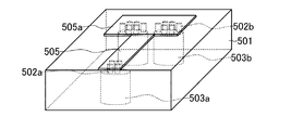
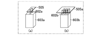
ところで、各第2孔部に対し、異なる数の第1孔部が接続するようにしてもよい。例えば、図5の斜視図に示すように、基板501の裏面側より形成する第2孔部503aには、4つの第1孔部502aが接続し、第2孔部503bには、6個の第1孔部502bが接続する構成としてもよい。第2孔部503aは、表面配線層505の形状に対応して配置し、第2孔部503bは、表面配線層505aの形状に対応して配置している。このようにすることで、例えば、第1孔部502aに接続する表面配線層505aに対し、第1孔部502bに接続する表面配線層505aの面積を大きくすることができ、表面配線層の形状自由度を向上させることができる。
By the way, a different number of first holes may be connected to each second hole. For example, as shown in the perspective view of FIG. 5, four
例えば、表面配線層の一部をランドメタル層とすることができるが、ランドメタル層は、パターンルールなどの制約が大きい。これに対し、上述したように、第2孔部に対して接続する第1孔部の数を調整し、また、第1孔部の寸法や配置を制御することで、より大きな自由度のある状態で、ランドメタル層が形成できるようにようになる。 For example, a part of the surface wiring layer can be a land metal layer, but the land metal layer has great restrictions such as pattern rules. On the other hand, as described above, there is a greater degree of freedom by adjusting the number of first holes connected to the second hole and controlling the size and arrangement of the first holes. In this state, the land metal layer can be formed.
なお、図5では、第1孔部および第2孔部103を円筒形状としたが、これに限るものではなく、図6の斜視図に示すように、第1孔部602a,第2孔部603a,第1孔部602b,および第2孔部603bの形状を、角柱としてもよい。なお、図6では、基板を省略して示している。
In FIG. 5, the first hole portion and the
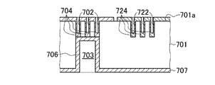
また、第1孔部の形成では、第1孔部とともに素子間分離のための溝部やキャパシタを構成する溝部を形成してもよい。例えば、図7に示すように、基板701の回路が形成されている主表面701aの側から、第1孔部702を形成するとともに、キャパシタを構成するためのトレンチ(溝部)722を形成する。次に、第1孔部配線704および表面配線層705を形成するとともに、キャパシタを構成するための一方の電極層724を形成する。この後、第1孔部702に接続する第2孔部703を形成する。この後、第1孔部配線704に接続する第2孔部配線706および裏面配線層707を形成する。このようにすることで、基板貫通ヴィアの微細化を図りながら、回路に使用されるキャパシタの高密度化をも図ることができる。また、プロセスを短縮化することができる。
In forming the first hole portion, a groove portion for separating elements and a groove portion constituting a capacitor may be formed together with the first hole portion. For example, as shown in FIG. 7, the
なお、本発明は以上に説明した実施の形態に限定されるものではなく、本発明の技術的思想内で、当分野において通常の知識を有する者により、多くの組み合わせおよび変形が実施可能であることは明白である。例えば、表面保護やエッチングストッパとして、基板の主表面,裏面、または各孔内に、SiO2,SiNおよび、有機材料からなる保護膜が形成されていてもよい。 The present invention is not limited to the embodiments described above, and many combinations and modifications can be implemented by those having ordinary knowledge in the art within the technical idea of the present invention. It is obvious. For example, as a surface protection or etching stopper, a protective film made of SiO 2 , SiN, and an organic material may be formed on the main surface, back surface, or each hole of the substrate.
101…基板、101a…主表面、102…第1孔部、103…第2孔部、104…第1孔部配線、105…表面配線層、106…第2孔部配線、107…裏面配線層。
DESCRIPTION OF
Claims (6)
前記基板の裏面側から形成されて前記第1孔部に接続する第2孔部と、
前記第1孔部の内部に形成された第1孔部配線と、
前記第1孔部配線に接続して前記基板の主表面側に形成された表面配線層と、
前記第2孔部の内部に前記第1孔部配線に接続して形成された第2孔部配線と、
前記第2孔部配線に接続して前記基板の裏面側に形成された裏面配線層と
を少なくとも備えることを特徴とするヴィア構造。 A first hole formed to a depth that can be formed in a range of a desired hole diameter from the main surface side where the circuit of the substrate is formed;
A second hole formed from the back side of the substrate and connected to the first hole;
A first hole wiring formed inside the first hole;
A surface wiring layer formed on the main surface side of the substrate connected to the first hole wiring;
A second hole wiring formed inside the second hole and connected to the first hole wiring;
A via structure connected to the second hole wiring and formed on the back surface side of the substrate.
前記第1孔部に接触する前記表面配線層で構成されたランドメタル層を備えることを特徴とするヴィア構造。 The via structure according to claim 1,
A via structure comprising a land metal layer composed of the surface wiring layer in contact with the first hole.
前記第1孔部の孔径は、2〜20μmであることを特徴とするヴィア構造。 The via structure according to claim 1 or 2,
The via structure has a hole diameter of 2 to 20 μm.
前記第1孔部の内部に第1孔部配線を形成する第2工程と、
前記基板の主表面側に前記第1孔部配線に接続する表面配線層を形成する第3工程と、
前記基板の裏面側から前記第1孔部に接続する第2孔部を形成する第4工程と、
前記第2孔部の内部に前記第1孔部配線に接続する第2孔部配線を形成する第5工程と、
前記基板の裏面側に前記第2孔部配線に接続する裏面配線層を形成する第6工程と
を少なくとも備えることを特徴とするヴィア構造の作製方法。 A first step of forming the first hole at a depth that can be formed in a range of a desired hole diameter from the main surface side where the circuit of the substrate is formed;
A second step of forming a first hole wiring inside the first hole;
A third step of forming a surface wiring layer connected to the first hole wiring on the main surface side of the substrate;
A fourth step of forming a second hole connected to the first hole from the back side of the substrate;
A fifth step of forming a second hole wiring connected to the first hole wiring inside the second hole;
And a sixth step of forming a back surface wiring layer connected to the second hole wiring on the back surface side of the substrate.
前記第1工程では、前記第1孔部とともに素子間分離のための溝部を形成することを特徴とするヴィア構造の作製方法。 The method for producing a via structure according to claim 4,
In the first step, a trench for separating elements is formed together with the first hole, and a via structure manufacturing method is provided.
前記第1工程では、前記第1孔部とともにキャパシタを構成する溝部を形成することを特徴とするヴィア構造の作製方法。 The method for producing a via structure according to claim 4,
In the first step, a groove part forming a capacitor is formed together with the first hole part.
Priority Applications (1)
| Application Number | Priority Date | Filing Date | Title |
|---|---|---|---|
| JP2011023684A JP2012164792A (en) | 2011-02-07 | 2011-02-07 | Via structure and manufacturing method thereof |
Applications Claiming Priority (1)
| Application Number | Priority Date | Filing Date | Title |
|---|---|---|---|
| JP2011023684A JP2012164792A (en) | 2011-02-07 | 2011-02-07 | Via structure and manufacturing method thereof |
Publications (1)
| Publication Number | Publication Date |
|---|---|
| JP2012164792A true JP2012164792A (en) | 2012-08-30 |
Family
ID=46843901
Family Applications (1)
| Application Number | Title | Priority Date | Filing Date |
|---|---|---|---|
| JP2011023684A Pending JP2012164792A (en) | 2011-02-07 | 2011-02-07 | Via structure and manufacturing method thereof |
Country Status (1)
| Country | Link |
|---|---|
| JP (1) | JP2012164792A (en) |
Cited By (1)
| Publication number | Priority date | Publication date | Assignee | Title |
|---|---|---|---|---|
| EP2893553A4 (en) * | 2012-09-05 | 2016-05-11 | Res Triangle Inst | Electronic devices utilizing contact pads with protrusions and methods for fabrication |
Citations (8)
| Publication number | Priority date | Publication date | Assignee | Title |
|---|---|---|---|---|
| JPH05102200A (en) * | 1991-10-03 | 1993-04-23 | Mitsubishi Electric Corp | Semiconductor device |
| JP2004349550A (en) * | 2003-05-23 | 2004-12-09 | Sharp Corp | Semiconductor device and its manufacturing method |
| JP2005294582A (en) * | 2004-03-31 | 2005-10-20 | Nec Electronics Corp | Method of manufacturing semiconductor device |
| JP2007081304A (en) * | 2005-09-16 | 2007-03-29 | Nippon Telegr & Teleph Corp <Ntt> | Semiconductor device and its manufacturing method |
| JP2007123681A (en) * | 2005-10-31 | 2007-05-17 | Sanyo Electric Co Ltd | Semiconductor device, manufacturing method thereof, and mounting substrate thereof |
| JP2007317954A (en) * | 2006-05-26 | 2007-12-06 | Nec Electronics Corp | Semiconductor device, and its manufacturing method |
| JP2009064820A (en) * | 2007-09-04 | 2009-03-26 | Toshiba Corp | Semiconductor device and method of manufacturing the same |
| JP2010531435A (en) * | 2007-06-06 | 2010-09-24 | ローベルト ボツシユ ゲゼルシヤフト ミツト ベシユレンクテル ハフツング | Micromechanical element and method for manufacturing micromechanical element |
-
2011
- 2011-02-07 JP JP2011023684A patent/JP2012164792A/en active Pending
Patent Citations (8)
| Publication number | Priority date | Publication date | Assignee | Title |
|---|---|---|---|---|
| JPH05102200A (en) * | 1991-10-03 | 1993-04-23 | Mitsubishi Electric Corp | Semiconductor device |
| JP2004349550A (en) * | 2003-05-23 | 2004-12-09 | Sharp Corp | Semiconductor device and its manufacturing method |
| JP2005294582A (en) * | 2004-03-31 | 2005-10-20 | Nec Electronics Corp | Method of manufacturing semiconductor device |
| JP2007081304A (en) * | 2005-09-16 | 2007-03-29 | Nippon Telegr & Teleph Corp <Ntt> | Semiconductor device and its manufacturing method |
| JP2007123681A (en) * | 2005-10-31 | 2007-05-17 | Sanyo Electric Co Ltd | Semiconductor device, manufacturing method thereof, and mounting substrate thereof |
| JP2007317954A (en) * | 2006-05-26 | 2007-12-06 | Nec Electronics Corp | Semiconductor device, and its manufacturing method |
| JP2010531435A (en) * | 2007-06-06 | 2010-09-24 | ローベルト ボツシユ ゲゼルシヤフト ミツト ベシユレンクテル ハフツング | Micromechanical element and method for manufacturing micromechanical element |
| JP2009064820A (en) * | 2007-09-04 | 2009-03-26 | Toshiba Corp | Semiconductor device and method of manufacturing the same |
Cited By (1)
| Publication number | Priority date | Publication date | Assignee | Title |
|---|---|---|---|---|
| EP2893553A4 (en) * | 2012-09-05 | 2016-05-11 | Res Triangle Inst | Electronic devices utilizing contact pads with protrusions and methods for fabrication |
Similar Documents
| Publication | Publication Date | Title |
|---|---|---|
| US9287172B2 (en) | Interposer-on-glass package method | |
| US9698104B2 (en) | Integrated electronic package and stacked assembly thereof | |
| US6693358B2 (en) | Semiconductor chip, wiring board and manufacturing process thereof as well as semiconductor device | |
| US7790608B2 (en) | Buried via technology for three dimensional integrated circuits | |
| US7795137B2 (en) | Manufacturing method of semiconductor device | |
| JP5576334B2 (en) | Semiconductor device, wiring board and manufacturing method thereof | |
| KR102625123B1 (en) | semiconductor device assembly | |
| JP2006253402A (en) | Manufacturing method of semiconductor device | |
| JPWO2011114774A1 (en) | Semiconductor element-embedded substrate and manufacturing method thereof | |
| JP2007067215A (en) | Circuit board, method of manufacturing circuit board and circuit device | |
| US8178977B2 (en) | Semiconductor device and method of manufacturing the same | |
| JP4678720B2 (en) | Circuit board and manufacturing method thereof, semiconductor device and manufacturing method thereof | |
| US20140370703A1 (en) | TSV Front-top Interconnection Process | |
| JP2006523943A (en) | Via and trench structures for semiconductor substrates bonded to metal substrates | |
| US20230092242A1 (en) | Dielectric layer separating a metal pad of a through glass via from a surface of the glass | |
| US20170330836A1 (en) | Cte compensation for wafer-level and chip-scale packages and assemblies | |
| JP6341554B2 (en) | Manufacturing method of semiconductor device | |
| JP2007012896A (en) | Circuit board, method of manufacturing same, and semiconductor device | |
| US20060128119A1 (en) | Semiconductor device fabrication method | |
| JP2012164792A (en) | Via structure and manufacturing method thereof | |
| JP2018010993A (en) | Electronic component and method of manufacturing the same | |
| KR101411734B1 (en) | Fabricating method of semiconductor device having through silicon via and semiconductor device therof | |
| US20230087838A1 (en) | Protective coating on an edge of a glass core | |
| US20230238305A1 (en) | Chip package and manufacturing method thereof | |
| TWI509761B (en) | Silicon based substrate and manufacturing method thereof |
Legal Events
| Date | Code | Title | Description |
|---|---|---|---|
| A621 | Written request for application examination |
Free format text: JAPANESE INTERMEDIATE CODE: A621 Effective date: 20121225 |
|
| A977 | Report on retrieval |
Free format text: JAPANESE INTERMEDIATE CODE: A971007 Effective date: 20140131 |
|
| A131 | Notification of reasons for refusal |
Free format text: JAPANESE INTERMEDIATE CODE: A131 Effective date: 20140225 |
|
| A521 | Written amendment |
Free format text: JAPANESE INTERMEDIATE CODE: A523 Effective date: 20140423 |
|
| A02 | Decision of refusal |
Free format text: JAPANESE INTERMEDIATE CODE: A02 Effective date: 20141202 |