JP2012137672A - Electronic apparatus - Google Patents
Electronic apparatus Download PDFInfo
- Publication number
- JP2012137672A JP2012137672A JP2010291095A JP2010291095A JP2012137672A JP 2012137672 A JP2012137672 A JP 2012137672A JP 2010291095 A JP2010291095 A JP 2010291095A JP 2010291095 A JP2010291095 A JP 2010291095A JP 2012137672 A JP2012137672 A JP 2012137672A
- Authority
- JP
- Japan
- Prior art keywords
- liquid crystal
- crystal panel
- light guide
- cover
- front cover
- Prior art date
- Legal status (The legal status is an assumption and is not a legal conclusion. Google has not performed a legal analysis and makes no representation as to the accuracy of the status listed.)
- Pending
Links
Images


Classifications
-
- G—PHYSICS
- G02—OPTICS
- G02F—OPTICAL DEVICES OR ARRANGEMENTS FOR THE CONTROL OF LIGHT BY MODIFICATION OF THE OPTICAL PROPERTIES OF THE MEDIA OF THE ELEMENTS INVOLVED THEREIN; NON-LINEAR OPTICS; FREQUENCY-CHANGING OF LIGHT; OPTICAL LOGIC ELEMENTS; OPTICAL ANALOGUE/DIGITAL CONVERTERS
- G02F1/00—Devices or arrangements for the control of the intensity, colour, phase, polarisation or direction of light arriving from an independent light source, e.g. switching, gating or modulating; Non-linear optics
- G02F1/01—Devices or arrangements for the control of the intensity, colour, phase, polarisation or direction of light arriving from an independent light source, e.g. switching, gating or modulating; Non-linear optics for the control of the intensity, phase, polarisation or colour
- G02F1/13—Devices or arrangements for the control of the intensity, colour, phase, polarisation or direction of light arriving from an independent light source, e.g. switching, gating or modulating; Non-linear optics for the control of the intensity, phase, polarisation or colour based on liquid crystals, e.g. single liquid crystal display cells
- G02F1/133—Constructional arrangements; Operation of liquid crystal cells; Circuit arrangements
- G02F1/1333—Constructional arrangements; Manufacturing methods
- G02F1/133308—Support structures for LCD panels, e.g. frames or bezels
-
- G—PHYSICS
- G02—OPTICS
- G02B—OPTICAL ELEMENTS, SYSTEMS OR APPARATUS
- G02B6/00—Light guides; Structural details of arrangements comprising light guides and other optical elements, e.g. couplings
- G02B6/0001—Light guides; Structural details of arrangements comprising light guides and other optical elements, e.g. couplings specially adapted for lighting devices or systems
- G02B6/0011—Light guides; Structural details of arrangements comprising light guides and other optical elements, e.g. couplings specially adapted for lighting devices or systems the light guides being planar or of plate-like form
- G02B6/0081—Mechanical or electrical aspects of the light guide and light source in the lighting device peculiar to the adaptation to planar light guides, e.g. concerning packaging
- G02B6/0085—Means for removing heat created by the light source from the package
-
- G—PHYSICS
- G02—OPTICS
- G02F—OPTICAL DEVICES OR ARRANGEMENTS FOR THE CONTROL OF LIGHT BY MODIFICATION OF THE OPTICAL PROPERTIES OF THE MEDIA OF THE ELEMENTS INVOLVED THEREIN; NON-LINEAR OPTICS; FREQUENCY-CHANGING OF LIGHT; OPTICAL LOGIC ELEMENTS; OPTICAL ANALOGUE/DIGITAL CONVERTERS
- G02F1/00—Devices or arrangements for the control of the intensity, colour, phase, polarisation or direction of light arriving from an independent light source, e.g. switching, gating or modulating; Non-linear optics
- G02F1/01—Devices or arrangements for the control of the intensity, colour, phase, polarisation or direction of light arriving from an independent light source, e.g. switching, gating or modulating; Non-linear optics for the control of the intensity, phase, polarisation or colour
- G02F1/13—Devices or arrangements for the control of the intensity, colour, phase, polarisation or direction of light arriving from an independent light source, e.g. switching, gating or modulating; Non-linear optics for the control of the intensity, phase, polarisation or colour based on liquid crystals, e.g. single liquid crystal display cells
- G02F1/133—Constructional arrangements; Operation of liquid crystal cells; Circuit arrangements
- G02F1/1333—Constructional arrangements; Manufacturing methods
- G02F1/133308—Support structures for LCD panels, e.g. frames or bezels
- G02F1/133314—Back frames
-
- G—PHYSICS
- G02—OPTICS
- G02F—OPTICAL DEVICES OR ARRANGEMENTS FOR THE CONTROL OF LIGHT BY MODIFICATION OF THE OPTICAL PROPERTIES OF THE MEDIA OF THE ELEMENTS INVOLVED THEREIN; NON-LINEAR OPTICS; FREQUENCY-CHANGING OF LIGHT; OPTICAL LOGIC ELEMENTS; OPTICAL ANALOGUE/DIGITAL CONVERTERS
- G02F1/00—Devices or arrangements for the control of the intensity, colour, phase, polarisation or direction of light arriving from an independent light source, e.g. switching, gating or modulating; Non-linear optics
- G02F1/01—Devices or arrangements for the control of the intensity, colour, phase, polarisation or direction of light arriving from an independent light source, e.g. switching, gating or modulating; Non-linear optics for the control of the intensity, phase, polarisation or colour
- G02F1/13—Devices or arrangements for the control of the intensity, colour, phase, polarisation or direction of light arriving from an independent light source, e.g. switching, gating or modulating; Non-linear optics for the control of the intensity, phase, polarisation or colour based on liquid crystals, e.g. single liquid crystal display cells
- G02F1/133—Constructional arrangements; Operation of liquid crystal cells; Circuit arrangements
- G02F1/1333—Constructional arrangements; Manufacturing methods
- G02F1/133308—Support structures for LCD panels, e.g. frames or bezels
- G02F1/133317—Intermediate frames, e.g. between backlight housing and front frame
-
- G—PHYSICS
- G02—OPTICS
- G02F—OPTICAL DEVICES OR ARRANGEMENTS FOR THE CONTROL OF LIGHT BY MODIFICATION OF THE OPTICAL PROPERTIES OF THE MEDIA OF THE ELEMENTS INVOLVED THEREIN; NON-LINEAR OPTICS; FREQUENCY-CHANGING OF LIGHT; OPTICAL LOGIC ELEMENTS; OPTICAL ANALOGUE/DIGITAL CONVERTERS
- G02F1/00—Devices or arrangements for the control of the intensity, colour, phase, polarisation or direction of light arriving from an independent light source, e.g. switching, gating or modulating; Non-linear optics
- G02F1/01—Devices or arrangements for the control of the intensity, colour, phase, polarisation or direction of light arriving from an independent light source, e.g. switching, gating or modulating; Non-linear optics for the control of the intensity, phase, polarisation or colour
- G02F1/13—Devices or arrangements for the control of the intensity, colour, phase, polarisation or direction of light arriving from an independent light source, e.g. switching, gating or modulating; Non-linear optics for the control of the intensity, phase, polarisation or colour based on liquid crystals, e.g. single liquid crystal display cells
- G02F1/133—Constructional arrangements; Operation of liquid crystal cells; Circuit arrangements
- G02F1/1333—Constructional arrangements; Manufacturing methods
- G02F1/133308—Support structures for LCD panels, e.g. frames or bezels
- G02F1/13332—Front frames
Abstract
Description
本発明の実施形態は、液晶パネルを有した電子機器に関する。 Embodiments described herein relate generally to an electronic apparatus having a liquid crystal panel.
テレビ等の電子機器において、液晶パネルのバックライト(光源)としてLEDを採用した商品が市場で主流になりつつある。また、近年、各部品メーカから様々な種類のLEDが供給され、バックライト用の高輝度のLEDも多数供給されている。 In electronic devices such as televisions, products that employ LEDs as backlights (light sources) for liquid crystal panels are becoming mainstream in the market. In recent years, various types of LEDs have been supplied from component manufacturers, and many high-brightness LEDs for backlights have also been supplied.
一方、光源周辺に蓄積された熱を外部に円滑に放出することが重要であることは、現在でも変わりはない。このため、このような放熱性の改良に対するニーズが存在していた。 On the other hand, the importance of smoothly releasing heat accumulated around the light source to the outside remains the same. Therefore, there is a need for such improvement in heat dissipation.
本発明は、放熱性を改良した電子機器を提供することを目的とする。 An object of this invention is to provide the electronic device which improved heat dissipation.
実施形態の電子機器は、液晶パネルと、前記液晶パネルの後方で、前記液晶パネルと向かい合った導光体と、前記液晶パネルの前方を覆った金属製で枠状のフロントカバーと、前記導光体の後方を覆った金属製のバックカバーと、前記フロントカバーと前記バックカバーとの間の位置で、前記フロントカバーと前記バックカバーとに当接して設けられるとともに、前記導光体の側面と向かい合った金属製の中間部材と、前記中間部材の内面に密着して設けられるとともに、複数のLEDが実装された基板と、を備えた。 An electronic apparatus according to an embodiment includes a liquid crystal panel, a light guide that faces the liquid crystal panel behind the liquid crystal panel, a metal frame-shaped front cover that covers the front of the liquid crystal panel, and the light guide A metal back cover that covers the back of the body, and is provided in contact with the front cover and the back cover at a position between the front cover and the back cover; A metal intermediate member facing each other, and a substrate provided in close contact with the inner surface of the intermediate member and mounted with a plurality of LEDs.
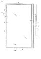
以下、図1から図3を参照して、電子機器の一例であるテレビの実施形態について説明する。図1に示すように、本実施形態にかかるテレビ11は、長方形の外観を有した薄型の表示装置である。図1に示すように、テレビ11は、本体12と、本体12を支持するスタンド13と、を備えている。
Hereinafter, with reference to FIGS. 1 to 3, an embodiment of a television as an example of an electronic device will be described. As shown in FIG. 1, the
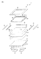
図1から図3に示すように、テレビ11は、第1面21Aおよび第2面21Bを有した液晶パネル21と、液晶パネル21の後方(第2面21B側)に設けられた板状の導光体22と、液晶パネル21の前方(第1面側21A)を覆った金属製で枠状のフロントカバー(第1カバー)23と、導光体22の後方(第2面21B側)を覆った金属製のバックカバー(第2カバー)24と、フロントカバー23とバックカバー24との間の位置に設けられた金属製の中間部材(ミドルフレーム)25と、中間部材25の内面に密着して設けられた基板26と、フロントカバー23、バックカバー24、および中間部材25を固定する固定部材の一例である第1ねじ27と、コントロール基板28およびLEDドライバ基板29と、コントロール基板28を覆う方形の第1シールドケース31と、LEDドライバ基板29を覆う方形の第2シールドケース32と、液晶パネル21とフロントカバー23との間に介在された第1断熱材33と、液晶パネル21と中間部材25との間に介在された第2断熱材34と、中間部材25と導光体22との間に介在された第3断熱材35と、を備えている。
As shown in FIGS. 1 to 3, the
液晶パネル21は、例えば2枚のガラス板を貼り合わせて形成されており、内部に液晶が封入されている。また、液晶パネル21の前面と後面には、それぞれ図示しない偏光板が貼り付けられている。図2に示すように、液晶パネル21は、ゲートドライバ36と、ソースドライバ37と、ソース基板38と、を含んでいる。
The
フロントカバー23は、金属材料、例えば熱伝導性の良好なアルミニウム合金によって枠状に形成されている。図1に示すように、フロントカバー23は、各辺を構成した計4個の棒状の部材41を、枠状をなすように連結して形成される。棒状の部材41は、それぞれ断面略「L」字形をなしている。
The
バックカバー24は、金属材料、例えばアルミニウム合金によって形成されている。中間部材25は、金属材料、例えばアルミニウム合金によって形成されている。
The
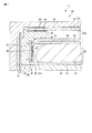
図2に示すように、中間部材25は、液晶パネル21の各辺に対応して計4個で構成され、それぞれ断面略「L」字形で棒状をなしている。図3に示すように、各中間部材25は、導光体22の側面22Aと向かい合っており、フロントカバー23とバックカバー24とに当接するように設けられている。中間部材25は、液晶パネル21および導光体22と略平行な方向に突出した突出部30を有している。突出部30は、突出部30とバックカバー24との間に導光体22を保持したり、突出部30とフロントカバー23との間に液晶パネル21を保持したりしている。
As shown in FIG. 2, the
基板26は、導光体22の側面22Aと向かい合うように設けられている。基板26は、例えば、アルミニウム合金等で形成された板状の基材42(ベース)と、基材42の一方の面に設けられ絶縁層と銅箔層とが交互に積層した配線部43と、配線部43の表面に設けられたバックライト用のLED44と、を有している。バックライト用のLED44は、半導体素子45と、半導体素子45の表面に設けられるとともに蛍光体を含んだ封止部材46と、を含んでいる。バックライト用のLED44は、配線部43の表面に複数個、横並びに設けられている。基材42は、第2ねじ47によって中間部材25の内面に固定されている。
The
第1断熱材33は、例えばゴムシートで構成されており、液晶パネル21とフロントカバー23とが衝突するのを防止する緩衝材を兼ねている。また、第2断熱材34は、例えばゴムシートで構成されており、液晶パネル21と中間部材25の突出部30とが衝突するのを防止する緩衝材を兼ねている。第3断熱材35は、例えばゴムシートで構成されており、中間部材25の突出部30と導光体22とが衝突するのを防止する緩衝材を兼ねている。
The first
導光体22は、液晶パネル21と向かい合って設けられている。導光体22は、例えば、板状の導光板51と、導光板51の前方に設けられたプリズムシート52と、プリズムシート52の前方に設けられた偏光シート53と、導光板51の後方に設けられた反射シート54と、を有している。導光体22は、導光板51、プリズムシート52、偏光シート53、および反射シート54を重ね合わせて構成されている。なお、本実施形態では、導光体22は、合計4枚のシートで構成されているが、他の種類のシートをさらに含んでいても良いし、枚数が少なくても構わない。
The
図3に示すように、LED44から照射された光は、導光板51の内部に照射され、プリズムシート52、偏光シート53を通過して、液晶パネル21を後方から照らすことができる。また、導光板51の内部に照射された光のうち、後方に向かって照射された光は、反射シート54で反射されて、プリズムシート52、偏光シート53を通過して、液晶パネル21を後方から照らすことができる。これによって、液晶パネル21において画像が表示される。
As shown in FIG. 3, the light emitted from the
本実施形態では、テレビ11を組み立てる際には、まず、フロントカバー23を枠状に組み立てる。そして、フロントカバー23に液晶パネル21をはめ込むようにする。この液晶パネル21に重ねて中間部材25を配置する。この中間部材25の内面には、バックライト用のLED44を実装した基板26が予め第1ねじ27で固定されている。さらに、中間部材25の突出部30に重ねて導光体22を配置する。最後に導光体22に重ねてバックカバー24を配置し、第1ねじ27によってフロントカバー23、バックカバー24、中間部材25を固定する。そして、バックカバー24に、コントロール基板28、LEDドライバ基板29、第1シールドケース31、および第2シールドケース32、を固定して本体12の組み立てが完了する。そして、この本体12にスタンド13を取り付けてテレビ11が完成する。
In the present embodiment, when the
第1の実施形態によれば、テレビ11は、液晶パネル21と、液晶パネル21の後方で、液晶パネル21と向かい合った導光体22と、液晶パネル21の前方を覆った金属製で枠状のフロントカバー23と、導光体22の後方を覆った金属製のバックカバー24と、フロントカバー23とバックカバー24との間の位置で、フロントカバー23とバックカバー24とに当接して設けられるとともに、導光体22の側面22Aと向かい合った金属製の中間部材25と、中間部材25の内面に密着して設けられるとともに、複数のLED44が実装された基板26と、を備える。
According to the first embodiment, the
一般に、バックライト用のLED44の熱がカバー内部に蓄積されると、当該熱が液晶パネル21に伝えられて、液晶パネル21に悪影響を及ぼす可能性がある。具体的には、液晶パネル21に熱が加えられると、内部の液晶の動き(反応性)が良くなり、液晶パネル21のうち熱が加えられた部分の画像にムラを生じたりする。また、液晶パネル21の前面と後面とにそれぞれ張り合わされた偏光板において熱膨張を生ずることがあり、その結果、偏光板が所望の機能を果たさなくなる恐れがある。
In general, when the heat of the
上記構成によれば、LED44から発生した熱を金属製の中間部材25に逃がすことができる。また、中間部材25は、金属製のフロントカバー23と、金属製のバックカバー24とに当接されているため、中間部材25に伝えられたLED44からの熱を、フロントカバー23およびバックカバー24にも伝達させることができる。これによって、LED44から発生した熱をフロントカバー23、バックカバー24、中間部材25に拡散できるとともに、フロントカバー23、バックカバー24、中間部材25においてその熱を外界に放出することができる。このため、LED44の熱が内部に蓄積されて、液晶パネル21等に悪影響を及ぼすことを極力防止することができる。
According to the above configuration, the heat generated from the
また、テレビ11は、液晶パネル21とフロントカバー23との間に介在された第1断熱材33と、液晶パネル21と中間部材25との間に介在された第2断熱材34と、を備える。この構成によれば、LED44からの熱がフロントカバー23および中間部材25を介して液晶パネル21に伝達されてしまうことを極力防止することができる。
The
続いて、図4を参照して、電子機器の一例であるテレビの第2の実施形態について説明する。第2の実施形態のテレビ11は、フロントカバー23と中間部材25とが一体になっている点、および中間部材25が省略されている点で第1の実施形態のものと異なっているが、他の部分は第1の実施形態と共通している。このため、主として異なる部分について説明し、共通する部分については共通の符号を付して説明を省略する。テレビ11は、図1に示す第1の実施形態のものと同様の外観を有する。
Next, a second embodiment of a television which is an example of an electronic device will be described with reference to FIG. The
フロントカバー(第1カバー)23は、液晶パネル21の前方を覆った枠状の前方部23Aと、導光体22の側面22Aと向かい合った側面部23Bと、を有している。フロントカバー23は、金属材料、例えば熱伝導性の良好なアルミニウム合金によって形成されている。側面部23Bは、バックカバー24と当接されている。側面部23Bは、液晶パネル21および導光体22と略平行な方向に突出した突出部30を有している。突出部30は、突出部30とバックカバー24との間に導光体22を保持したり、突出部30と前方部23Aとの間に液晶パネル21を保持したりできる。
The front cover (first cover) 23 includes a frame-shaped
フロントカバー23は、各辺を構成した計4個の棒状の部材41を、枠状をなすように連結して形成される。
The
基板26は、側面部23Bの内面に密着して設けられている。基板26は、導光体22の側面22Aと向かい合っている。基板26は、第2ねじ47によって側面部23Bに固定されている。基板26の構造は、第1の実施形態と同様である。
The
第1断熱材33は、液晶パネル21とフロントカバー23の前方部との間に介在されている。第2断熱材34は、液晶パネル21と側面部23Bの突出部30との間に介在されている。第3断熱材35は、側面部23Bの突出部30と導光体22との間に介在されている。
The first
本実施形態では、フロントカバー23を枠組みする際には、枠の内側に液晶パネル21をはめ込むようにする。フロントカバー23が枠組みされた状態において、液晶パネル21は、前方部23Aと突出部30との間の位置に保持される。このフロントカバー23に対して導光体22およびバックカバー24を取り付けて、テレビ11の本体12の組み立てが完了する。この本体12にスタンド13を取り付けてテレビ11が完成する。
In the present embodiment, when the
第2の実施形態によれば、テレビ11は、液晶パネル21と、液晶パネル21の後方で、液晶パネル21と向かい合った導光体22と、導光体22の後方を覆った金属製のバックカバー24と、液晶パネル21の前方を覆った枠状の前方部23Aと、バックカバー24と当接されるとともに導光体22の側面22Aと向かい合った側面部23Bと、を有した金属製のフロントカバー23と、側面部23Bの内面に密着して設けられるとともに、複数のLED44が実装された基板26と、を備える。
According to the second embodiment, the
この構成によれば、LED44から発生した熱を金属製のフロントカバー23の側面部23Bに逃がすことができる。また、側面部23Bは、金属製のバックカバー24に当接されているため、側面部23Bに伝えられたLEDからの熱を、バックカバー24およびフロントカバー23の前方部23Aにも伝達させることができる。これによって、LED44から発生した熱をフロントカバー23およびバックカバー24に拡散できるとともに、当該熱をフロントカバー23およびバックカバー24において外界に放出することができる。このため、LED44の熱が内部に蓄積されて、液晶パネル21等に悪影響を及ぼすことを極力防止することができる。
According to this configuration, heat generated from the
続いて、図5を参照して、電子機器の一例であるテレビの第3の実施形態について説明する。第3の実施形態のテレビ11は、バックカバー24と中間部材25とが一体になっている点、および中間部材25が省略されている点で第1の実施形態のものと異なっているが、他の部分は第1の実施形態と共通している。このため、主として異なる部分について説明し、共通する部分については共通の符号を付して説明を省略する。テレビ11は、図1に示す第1の実施形態のものと同様の外観を有する。
Next, a third embodiment of a television which is an example of an electronic device will be described with reference to FIG. The
バックカバー(第2カバー)24は、液晶パネル21の後方(第2面側21B)を覆った板状の後方部(覆部)24Aと、導光体22の側面22Aと向かい合った側面部24Bと、を有している。バックカバー24は、金属材料、例えば熱伝導性の良好なアルミニウム合金によって形成されている。側面部24Bは、フロントカバー(第1カバー)23と当接されている。側面部24Bは、液晶パネル21および導光体22と略平行な方向に突出した突出部30を有している。突出部30は、突出部30と後方部(覆部)24Aとの間に導光体22を保持したり、突出部30とフロントカバー23との間に液晶パネル21を保持したりできる。
The back cover (second cover) 24 includes a plate-like rear part (covering part) 24A that covers the rear side (
基板26は、側面部24Bの内面に密着して設けられている。基板26は、導光体22の側面22Aと向かい合っている。基板26は、第2ねじ47によって側面部24Bに固定されている。基板26の構造は、第1の実施形態と同様である。
The
第1断熱材33は、液晶パネル21とフロントカバー23との間に介在されている。第2断熱材34は、液晶パネル21と側面部24Bの突出部30との間に介在されている。第3断熱材35は、側面部24Bの突出部30と導光体22との間に介在されている。
The first
本実施形態では、バックカバー24は、例えば、その幅方向Wにおける中間部において、第1の部分と第2の部分とに2分割されている。バックカバー24を組み立てる際には、予め側面部24Bの突出部30と後方部24Aとの間の位置に導光体22を嵌め入れた状態で、第1の部分と第2の部分とを例えばねじ等で固定して、一体のバックカバー24を構成する。その後、この一体のバックカバー24に液晶パネル21を装着するとともに、液晶パネル21に重ねてフロントカバー23を配置する。第1ねじ27によってバックカバー24とフロントカバー23とを固定することで、テレビ11の本体12が完成する。この本体12にスタンド13を取り付けてテレビ11が完成する。
In the present embodiment, the
第3の実施形態によれば、テレビ11は、液晶パネル21と、液晶パネル21の後方で、液晶パネル21と向かい合った導光体22と、液晶パネル21の前方を覆った金属製で枠状のフロントカバー23と、導光体22の後方を覆った後方部24Aと、フロントカバー23と当接されるとともに導光体22の側面22Aと向かい合った側面部24Bと、を有した金属製のバックカバー24と、側面部24Bの内面に密着して設けられるとともに、複数のLED44が実装された基板26と、を備える。
According to the third embodiment, the
この構成によれば、LED44から発生した熱を金属製のバックカバー24の側面部24Bに逃がすことができる。また、側面部24Bは、金属製のフロントカバー23に当接されているため、側面部24Bに伝えられたLED44からの熱を、フロントカバー23および後方部24Aにも伝達させることができる。これによって、LED44から発生した熱をフロントカバー23およびバックカバー24に拡散できるとともに、当該熱をフロントカバー23およびバックカバー24において外界に放出することができる。このため、LED44の熱が内部に蓄積されて、液晶パネル21等に悪影響を及ぼすことを極力防止することができる。
According to this configuration, heat generated from the
電子機器は、上記実施形態に示したテレビ11に限定されるものではなく、例えば、ポータブルコンピュータや携帯電話機、書籍や画像等を電子的に表示する電子ブックリーダーのようなその他の電子機器に対しても当然に実施可能である。
The electronic device is not limited to the
さらに、電子機器は上記実施形態そのままに限定されるものではなく、実施段階ではその要旨を逸脱しない範囲で構成要素を変形して具体化できる。さらに、上記実施形態に開示されている複数の構成要素の適宜な組み合わせにより種々の発明を形成できる。例えば、実施形態に示される全構成要素から幾つかの構成要素を削除してもよい。更に、異なる実施形態に亘る構成要素を適宜組み合わせてもよい。 Further, the electronic device is not limited to the above-described embodiment as it is, and can be embodied by modifying the constituent elements without departing from the scope of the invention in the implementation stage. Furthermore, various inventions can be formed by appropriately combining a plurality of constituent elements disclosed in the embodiment. For example, some components may be deleted from all the components shown in the embodiment. Furthermore, you may combine the component covering different embodiment suitably.
11…テレビ、21…液晶パネル、22…導光体、22A…側面、23…フロントカバー、23A…前方部、23B…側面部、24…バックカバー、24A…後方部、24B…側面部、25…中間部材、26…基板、27…第1ねじ、33…第1断熱材、34…第2断熱材、42…基材
DESCRIPTION OF
さらに、電子機器は上記実施形態そのままに限定されるものではなく、実施段階ではその要旨を逸脱しない範囲で構成要素を変形して具体化できる。さらに、上記実施形態に開示されている複数の構成要素の適宜な組み合わせにより種々の発明を形成できる。例えば、実施形態に示される全構成要素から幾つかの構成要素を削除してもよい。更に、異なる実施形態に亘る構成要素を適宜組み合わせてもよい。
以下に、本願出願の当初の特許請求の範囲に記載された発明を付記する。
[1]
液晶パネルと、
前記液晶パネルの後方で、前記液晶パネルと向かい合った導光体と、
前記液晶パネルの前方を覆った金属製で枠状のフロントカバーと、
前記導光体の後方を覆った金属製のバックカバーと、
前記フロントカバーと前記バックカバーとの間の位置で、前記フロントカバーと前記バックカバーとに当接して設けられるとともに、前記導光体の側面と向かい合った金属製の中間部材と、
前記中間部材の内面に密着して設けられるとともに、複数のLEDが実装された基板と、
を備えた電子機器。
[2]
前記液晶パネルと前記フロントカバーとの間に介在された第1断熱材と、
前記液晶パネルと前記中間部材との間に介在された第2断熱材と、
を備えた[1]に記載の電子機器。
[3]
液晶パネルと、
前記液晶パネルの後方で、前記液晶パネルと向かい合った導光体と、
前記導光体の後方を覆った金属製のバックカバーと、
前記液晶パネルの前方を覆った枠状の前方部と、前記バックカバーと当接されるとともに前記導光体の側面と向かい合った側面部と、を有した金属製のフロントカバーと、
前記側面部の内面に密着して設けられるとともに、複数のLEDが実装された基板と、
を備えた電子機器。
[4]
前記液晶パネルと前記前方部との間に介在された第1断熱材と、
前記液晶パネルと前記側面部との間に介在された第2断熱材と、
を備えた[3]に記載の電子機器。
[5]
第1面と、この第1面とは反対側に設けられた第2面とを有した液晶パネルと、
前記液晶パネルの前記第2面側で、前記液晶パネルと向かい合った導光体と、
前記液晶パネルの前記第1面側を覆った金属製で枠状の第1カバーと、
前記液晶パネルの前記第2面側から前記導光体を覆った覆部と、前記第1カバーと当接されて前記導光体の側面と向かい合った側面部と、を有した金属製の第2カバーと、
前記側面部の内面に当接され、複数のLEDが実装された基板と、
を備えた電子機器。
[6]
前記液晶パネルと前記第1カバーとの間に介在された第1断熱材と、
前記液晶パネルと前記側面部との間に介在された第2断熱材と、
を備えた[5]に記載の電子機器。
Further, the electronic device is not limited to the above-described embodiment as it is, and can be embodied by modifying the constituent elements without departing from the scope of the invention in the implementation stage. Furthermore, various inventions can be formed by appropriately combining a plurality of constituent elements disclosed in the embodiment. For example, some components may be deleted from all the components shown in the embodiment. Furthermore, you may combine the component covering different embodiment suitably.
Hereinafter, the invention described in the scope of claims of the present application will be appended.
[1]
LCD panel,
A light guide facing the liquid crystal panel behind the liquid crystal panel;
A metal frame-shaped front cover covering the front of the liquid crystal panel;
A metal back cover covering the back of the light guide;
A metal intermediate member provided in contact with the front cover and the back cover at a position between the front cover and the back cover and facing a side surface of the light guide;
Provided in close contact with the inner surface of the intermediate member, a substrate on which a plurality of LEDs are mounted,
With electronic equipment.
[2]
A first heat insulating material interposed between the liquid crystal panel and the front cover;
A second heat insulating material interposed between the liquid crystal panel and the intermediate member;
The electronic device according to [1], comprising:
[3]
LCD panel,
A light guide facing the liquid crystal panel behind the liquid crystal panel;
A metal back cover covering the back of the light guide;
A metal front cover having a frame-shaped front portion that covers the front of the liquid crystal panel, and a side portion that is in contact with the back cover and faces the side surface of the light guide;
Provided in close contact with the inner surface of the side portion, a substrate on which a plurality of LEDs are mounted,
With electronic equipment.
[4]
A first heat insulating material interposed between the liquid crystal panel and the front portion;
A second heat insulating material interposed between the liquid crystal panel and the side surface;
The electronic device according to [3], comprising:
[5]
A liquid crystal panel having a first surface and a second surface provided on the opposite side of the first surface;
A light guide facing the liquid crystal panel on the second surface side of the liquid crystal panel;
A metal frame-shaped first cover that covers the first surface side of the liquid crystal panel;
A metal first having a cover that covers the light guide from the second surface side of the liquid crystal panel, and a side that is in contact with the first cover and faces the side of the light guide. Two covers,
A substrate that is in contact with the inner surface of the side surface portion and on which a plurality of LEDs are mounted;
With electronic equipment.
[6]
A first heat insulating material interposed between the liquid crystal panel and the first cover;
A second heat insulating material interposed between the liquid crystal panel and the side surface;
The electronic device according to [5], comprising:
Claims (6)
前記液晶パネルの後方で、前記液晶パネルと向かい合った導光体と、
前記液晶パネルの前方を覆った金属製で枠状のフロントカバーと、
前記導光体の後方を覆った金属製のバックカバーと、
前記フロントカバーと前記バックカバーとの間の位置で、前記フロントカバーと前記バックカバーとに当接して設けられるとともに、前記導光体の側面と向かい合った金属製の中間部材と、
前記中間部材の内面に密着して設けられるとともに、複数のLEDが実装された基板と、
を備えた電子機器。 LCD panel,
A light guide facing the liquid crystal panel behind the liquid crystal panel;
A metal frame-shaped front cover covering the front of the liquid crystal panel;
A metal back cover covering the back of the light guide;
A metal intermediate member provided in contact with the front cover and the back cover at a position between the front cover and the back cover and facing a side surface of the light guide;
Provided in close contact with the inner surface of the intermediate member, a substrate on which a plurality of LEDs are mounted,
With electronic equipment.
前記液晶パネルと前記中間部材との間に介在された第2断熱材と、
を備えた請求項1に記載の電子機器。 A first heat insulating material interposed between the liquid crystal panel and the front cover;
A second heat insulating material interposed between the liquid crystal panel and the intermediate member;
The electronic device according to claim 1, further comprising:
前記液晶パネルの後方で、前記液晶パネルと向かい合った導光体と、
前記導光体の後方を覆った金属製のバックカバーと、
前記液晶パネルの前方を覆った枠状の前方部と、前記バックカバーと当接されるとともに前記導光体の側面と向かい合った側面部と、を有した金属製のフロントカバーと、
前記側面部の内面に密着して設けられるとともに、複数のLEDが実装された基板と、
を備えた電子機器。 LCD panel,
A light guide facing the liquid crystal panel behind the liquid crystal panel;
A metal back cover covering the back of the light guide;
A metal front cover having a frame-shaped front portion that covers the front of the liquid crystal panel, and a side portion that is in contact with the back cover and faces the side surface of the light guide;
Provided in close contact with the inner surface of the side portion, a substrate on which a plurality of LEDs are mounted,
With electronic equipment.
前記液晶パネルと前記側面部との間に介在された第2断熱材と、
を備えた請求項3に記載の電子機器。 A first heat insulating material interposed between the liquid crystal panel and the front portion;
A second heat insulating material interposed between the liquid crystal panel and the side surface;
The electronic device according to claim 3, further comprising:
前記液晶パネルの前記第2面側で、前記液晶パネルと向かい合った導光体と、
前記液晶パネルの前記第1面側を覆った金属製で枠状の第1カバーと、
前記液晶パネルの前記第2面側から前記導光体を覆った覆部と、前記第1カバーと当接されて前記導光体の側面と向かい合った側面部と、を有した金属製の第2カバーと、
前記側面部の内面に当接され、複数のLEDが実装された基板と、
を備えた電子機器。 A liquid crystal panel having a first surface and a second surface provided on the opposite side of the first surface;
A light guide facing the liquid crystal panel on the second surface side of the liquid crystal panel;
A metal frame-shaped first cover that covers the first surface side of the liquid crystal panel;
A metal first having a cover that covers the light guide from the second surface side of the liquid crystal panel, and a side that is in contact with the first cover and faces the side of the light guide. Two covers,
A substrate that is in contact with the inner surface of the side surface portion and on which a plurality of LEDs are mounted;
With electronic equipment.
前記液晶パネルと前記側面部との間に介在された第2断熱材と、
を備えた請求項5に記載の電子機器。 A first heat insulating material interposed between the liquid crystal panel and the first cover;
A second heat insulating material interposed between the liquid crystal panel and the side surface;
The electronic device according to claim 5, comprising:
Priority Applications (2)
| Application Number | Priority Date | Filing Date | Title |
|---|---|---|---|
| JP2010291095A JP2012137672A (en) | 2010-12-27 | 2010-12-27 | Electronic apparatus |
| US13/295,387 US20120162567A1 (en) | 2010-12-27 | 2011-11-14 | Electronic device |
Applications Claiming Priority (1)
| Application Number | Priority Date | Filing Date | Title |
|---|---|---|---|
| JP2010291095A JP2012137672A (en) | 2010-12-27 | 2010-12-27 | Electronic apparatus |
Related Child Applications (1)
| Application Number | Title | Priority Date | Filing Date |
|---|---|---|---|
| JP2012255596A Division JP5550708B2 (en) | 2012-11-21 | 2012-11-21 | Electronics |
Publications (1)
| Publication Number | Publication Date |
|---|---|
| JP2012137672A true JP2012137672A (en) | 2012-07-19 |
Family
ID=46316297
Family Applications (1)
| Application Number | Title | Priority Date | Filing Date |
|---|---|---|---|
| JP2010291095A Pending JP2012137672A (en) | 2010-12-27 | 2010-12-27 | Electronic apparatus |
Country Status (2)
| Country | Link |
|---|---|
| US (1) | US20120162567A1 (en) |
| JP (1) | JP2012137672A (en) |
Cited By (6)
| Publication number | Priority date | Publication date | Assignee | Title |
|---|---|---|---|---|
| JP2013058468A (en) * | 2011-08-17 | 2013-03-28 | Seiko Epson Corp | Liquid crystal display and electronic equipment |
| JP2013148880A (en) * | 2011-06-07 | 2013-08-01 | Sharp Corp | Display device and television receiver |
| JP2013243786A (en) * | 2013-09-10 | 2013-12-05 | Sharp Corp | Display device and television receiver |
| JPWO2013047366A1 (en) * | 2011-09-30 | 2015-03-26 | シャープ株式会社 | Display device and television receiver |
| US9091418B2 (en) | 2011-06-07 | 2015-07-28 | Sharp Kabushiki Kaisha | Display device and television receiver |
| JP2016110064A (en) * | 2014-12-09 | 2016-06-20 | 揚昇照明股▲ふん▼有限公司 | Display device and backlight module |
Families Citing this family (5)
| Publication number | Priority date | Publication date | Assignee | Title |
|---|---|---|---|---|
| JP5032651B2 (en) | 2010-12-27 | 2012-09-26 | 株式会社東芝 | Television receiver and electronic device |
| JP5159872B2 (en) | 2010-12-27 | 2013-03-13 | 株式会社東芝 | Television receiver |
| JP2015004709A (en) * | 2013-06-19 | 2015-01-08 | 三菱電機株式会社 | Display device |
| CN203849520U (en) * | 2014-05-27 | 2014-09-24 | 北京京东方显示技术有限公司 | Display device |
| KR102224632B1 (en) * | 2014-11-07 | 2021-03-08 | 엘지전자 주식회사 | Display apparatus |
Citations (6)
| Publication number | Priority date | Publication date | Assignee | Title |
|---|---|---|---|---|
| JP2001184924A (en) * | 1999-12-24 | 2001-07-06 | Sanyo Electric Co Ltd | Plane light source apparatus |
| WO2007039975A1 (en) * | 2005-09-30 | 2007-04-12 | Sharp Kabushiki Kaisha | Illuminating device and display using same |
| JP2007265837A (en) * | 2006-03-29 | 2007-10-11 | Epson Imaging Devices Corp | Frame for lighting system, lighting system and display device |
| JP2009098310A (en) * | 2007-10-15 | 2009-05-07 | Hitachi Displays Ltd | Liquid crystal display device |
| JP2010067439A (en) * | 2008-09-10 | 2010-03-25 | Harison Toshiba Lighting Corp | Surface light-emitting device, and display device |
| JP2010122429A (en) * | 2008-11-19 | 2010-06-03 | Kyocera Corp | Liquid crystal display and electronic device provided with the same |
Family Cites Families (11)
| Publication number | Priority date | Publication date | Assignee | Title |
|---|---|---|---|---|
| US5640216A (en) * | 1994-04-13 | 1997-06-17 | Hitachi, Ltd. | Liquid crystal display device having video signal driving circuit mounted on one side and housing |
| JP2003167235A (en) * | 2001-12-03 | 2003-06-13 | Nec Kagoshima Ltd | Assembling structure of liquid crystal display device, and its assembling method |
| TW590199U (en) * | 2002-11-13 | 2004-06-01 | Hon Hai Prec Ind Co Ltd | Surface lighting module |
| JP4654920B2 (en) * | 2006-01-19 | 2011-03-23 | 三菱電機株式会社 | Light source device and liquid crystal display device |
| JP2008083584A (en) * | 2006-09-28 | 2008-04-10 | Nec Lcd Technologies Ltd | Liquid crystal panel module and liquid crystal display device |
| CN101589267A (en) * | 2007-01-22 | 2009-11-25 | 夏普株式会社 | Backlight device and flat display using it |
| US20080225202A1 (en) * | 2007-03-15 | 2008-09-18 | Hanbitt Joo | Optical sheet and liquid crystal display device having the same |
| KR101326579B1 (en) * | 2007-05-25 | 2013-11-20 | 엘지디스플레이 주식회사 | Liquid crystal display device |
| JP5024793B2 (en) * | 2007-10-19 | 2012-09-12 | Nltテクノロジー株式会社 | Display device |
| JP5190735B2 (en) * | 2008-03-06 | 2013-04-24 | Nltテクノロジー株式会社 | Backlight and liquid crystal display device |
| JP5212222B2 (en) * | 2009-03-30 | 2013-06-19 | 富士通株式会社 | Mobile terminal device |
-
2010
- 2010-12-27 JP JP2010291095A patent/JP2012137672A/en active Pending
-
2011
- 2011-11-14 US US13/295,387 patent/US20120162567A1/en not_active Abandoned
Patent Citations (6)
| Publication number | Priority date | Publication date | Assignee | Title |
|---|---|---|---|---|
| JP2001184924A (en) * | 1999-12-24 | 2001-07-06 | Sanyo Electric Co Ltd | Plane light source apparatus |
| WO2007039975A1 (en) * | 2005-09-30 | 2007-04-12 | Sharp Kabushiki Kaisha | Illuminating device and display using same |
| JP2007265837A (en) * | 2006-03-29 | 2007-10-11 | Epson Imaging Devices Corp | Frame for lighting system, lighting system and display device |
| JP2009098310A (en) * | 2007-10-15 | 2009-05-07 | Hitachi Displays Ltd | Liquid crystal display device |
| JP2010067439A (en) * | 2008-09-10 | 2010-03-25 | Harison Toshiba Lighting Corp | Surface light-emitting device, and display device |
| JP2010122429A (en) * | 2008-11-19 | 2010-06-03 | Kyocera Corp | Liquid crystal display and electronic device provided with the same |
Cited By (8)
| Publication number | Priority date | Publication date | Assignee | Title |
|---|---|---|---|---|
| JP2013148880A (en) * | 2011-06-07 | 2013-08-01 | Sharp Corp | Display device and television receiver |
| JP2013150306A (en) * | 2011-06-07 | 2013-08-01 | Sharp Corp | Display device and television receiver |
| US9091418B2 (en) | 2011-06-07 | 2015-07-28 | Sharp Kabushiki Kaisha | Display device and television receiver |
| JP2013058468A (en) * | 2011-08-17 | 2013-03-28 | Seiko Epson Corp | Liquid crystal display and electronic equipment |
| US9664951B2 (en) | 2011-08-17 | 2017-05-30 | Seiko Epson Corporation | Liquid crystal display device and electronic device |
| JPWO2013047366A1 (en) * | 2011-09-30 | 2015-03-26 | シャープ株式会社 | Display device and television receiver |
| JP2013243786A (en) * | 2013-09-10 | 2013-12-05 | Sharp Corp | Display device and television receiver |
| JP2016110064A (en) * | 2014-12-09 | 2016-06-20 | 揚昇照明股▲ふん▼有限公司 | Display device and backlight module |
Also Published As
| Publication number | Publication date |
|---|---|
| US20120162567A1 (en) | 2012-06-28 |
Similar Documents
| Publication | Publication Date | Title |
|---|---|---|
| JP2012137672A (en) | Electronic apparatus | |
| JP5933509B2 (en) | Liquid crystal display | |
| KR101001405B1 (en) | Liquid crystal display device | |
| US9467641B2 (en) | Television and electronic apparatus | |
| US9279933B2 (en) | Dual-sided display device and its backlight module | |
| JP5032650B2 (en) | TV and electronics | |
| JP6374323B2 (en) | Display device | |
| WO2015002017A1 (en) | Illumination device, display device, and television receiving device | |
| WO2015059965A1 (en) | Display device and television receiver | |
| WO2014021209A1 (en) | Illumination device, display device, and tv reception device | |
| WO2014034633A1 (en) | Lighting apparatus, display apparatus, and television receiver | |
| US10345510B2 (en) | Liquid crystal display | |
| WO2014073425A1 (en) | Illumination device, display device, and television receiver device | |
| WO2011086814A1 (en) | Lighting device, display apparatus, and television receiver apparatus | |
| JP2013218055A (en) | Display device and television receiver | |
| WO2013191051A1 (en) | Display, and television receiver | |
| JP2016224090A (en) | Backlight and display | |
| JP6529354B2 (en) | Light source device and display device | |
| WO2013031672A1 (en) | Illumination device, display device, and television reception device | |
| JP2014074756A (en) | Display device and television receiver | |
| JP2014178551A (en) | Liquid crystal display device | |
| JP2013171619A (en) | Display device, and television receiver | |
| JP2013206574A (en) | Lighting device, display device, and tv receiver | |
| JP5721660B2 (en) | Display device and television receiver | |
| WO2014141882A1 (en) | Display apparatus and television receiving apparatus |
Legal Events
| Date | Code | Title | Description |
|---|---|---|---|
| A131 | Notification of reasons for refusal |
Free format text: JAPANESE INTERMEDIATE CODE: A131 Effective date: 20120529 |
|
| A521 | Written amendment |
Free format text: JAPANESE INTERMEDIATE CODE: A523 Effective date: 20120727 |
|
| A02 | Decision of refusal |
Free format text: JAPANESE INTERMEDIATE CODE: A02 Effective date: 20120821 |