JP2012133836A - Resistance change type memory - Google Patents
Resistance change type memory Download PDFInfo
- Publication number
- JP2012133836A JP2012133836A JP2010283204A JP2010283204A JP2012133836A JP 2012133836 A JP2012133836 A JP 2012133836A JP 2010283204 A JP2010283204 A JP 2010283204A JP 2010283204 A JP2010283204 A JP 2010283204A JP 2012133836 A JP2012133836 A JP 2012133836A
- Authority
- JP
- Japan
- Prior art keywords
- cell
- potential
- line
- bit line
- current
- Prior art date
- Legal status (The legal status is an assumption and is not a legal conclusion. Google has not performed a legal analysis and makes no representation as to the accuracy of the status listed.)
- Withdrawn
Links
Images


Classifications
-
- G—PHYSICS
- G11—INFORMATION STORAGE
- G11C—STATIC STORES
- G11C11/00—Digital stores characterised by the use of particular electric or magnetic storage elements; Storage elements therefor
- G11C11/02—Digital stores characterised by the use of particular electric or magnetic storage elements; Storage elements therefor using magnetic elements
- G11C11/16—Digital stores characterised by the use of particular electric or magnetic storage elements; Storage elements therefor using magnetic elements using elements in which the storage effect is based on magnetic spin effect
- G11C11/161—Digital stores characterised by the use of particular electric or magnetic storage elements; Storage elements therefor using magnetic elements using elements in which the storage effect is based on magnetic spin effect details concerning the memory cell structure, e.g. the layers of the ferromagnetic memory cell
-
- G—PHYSICS
- G11—INFORMATION STORAGE
- G11C—STATIC STORES
- G11C11/00—Digital stores characterised by the use of particular electric or magnetic storage elements; Storage elements therefor
- G11C11/02—Digital stores characterised by the use of particular electric or magnetic storage elements; Storage elements therefor using magnetic elements
- G11C11/16—Digital stores characterised by the use of particular electric or magnetic storage elements; Storage elements therefor using magnetic elements using elements in which the storage effect is based on magnetic spin effect
- G11C11/165—Auxiliary circuits
- G11C11/1659—Cell access
-
- G—PHYSICS
- G11—INFORMATION STORAGE
- G11C—STATIC STORES
- G11C11/00—Digital stores characterised by the use of particular electric or magnetic storage elements; Storage elements therefor
- G11C11/02—Digital stores characterised by the use of particular electric or magnetic storage elements; Storage elements therefor using magnetic elements
- G11C11/16—Digital stores characterised by the use of particular electric or magnetic storage elements; Storage elements therefor using magnetic elements using elements in which the storage effect is based on magnetic spin effect
- G11C11/165—Auxiliary circuits
- G11C11/1673—Reading or sensing circuits or methods
Landscapes
- Engineering & Computer Science (AREA)
- Computer Hardware Design (AREA)
- Mram Or Spin Memory Techniques (AREA)
- Hall/Mr Elements (AREA)
Abstract
Description
本発明の実施形態は、抵抗変化型メモリに関する。 Embodiments described herein relate generally to a resistance change type memory.
近年、次世代半導体メモリとして、MRAM(Magnetoresistive RAM)、ReRAM(Resistive RAM)、及び、PCRAM(Phase change RAM)などの抵抗変化型メモリが注目を集めている。 In recent years, resistance change type memories such as MRAM (Magnetoresistive RAM), ReRAM (Resistive RAM), and PCRAM (Phase change RAM) have attracted attention as next-generation semiconductor memories.
抵抗変化型メモリのセルアレイにおいて、複数のメモリセルが2次元に配列されている。複数のメモリセルが、共通の配線及び回路に接続されている。 In the resistance change memory cell array, a plurality of memory cells are two-dimensionally arranged. A plurality of memory cells are connected to a common wiring and circuit.
例えば、データの読み出し時、データの読み出し対象として選択されたメモリセルは、非選択のメモリセルと共通の配線及び回路に接続される。 For example, when reading data, a memory cell selected as a data read target is connected to a common wiring and circuit with a non-selected memory cell.
このため、非選択のメモリセルが、選択されたメモリセルの動作に対して影響を及ぼす場合がある。 For this reason, unselected memory cells may affect the operation of the selected memory cell.
データ読み出しの精度の向上を図る。 Improve the accuracy of data reading.
本実施形態の抵抗変化型メモリは、ビット線及びソース線と、複数のワード線と、抵抗変化型メモリ素子と前記ワード線に接続されるゲートを有するセルトランジスタとをそれぞれ含み、前記ビット線と前記ソース線との間に接続される複数のメモリセルと、第1の制御電圧が印加される第1のゲートと、前記ビット線に接続される第1の電流経路とを有するnチャネル型の第1の電界効果トランジスタと、第2の制御電圧が印加される第2のゲートと、前記ソース線に接続される第2の電流経路とを有するpチャネル型の第2の電界効果トランジスタと、を具備し、選択されたメモリセルに対するデータの読み出し時、前記ビット線の電位は前記第1の制御電圧によって制御され、前記ソース線の電位は前記第2の制御電圧によって制御され、前記ビット線の電位は、前記ソース線の電位より大きく、前記選択されたメモリセルが接続されたワード線の電位は、前記ビット線の電位より大きく、非選択のメモリセルが接続されたワード線の電位は、前記ソース線の電位より小さい。 The resistance change type memory according to this embodiment includes a bit line and a source line, a plurality of word lines, a resistance change type memory element, and a cell transistor having a gate connected to the word line, An n-channel type having a plurality of memory cells connected to the source line, a first gate to which a first control voltage is applied, and a first current path connected to the bit line A p-channel type second field effect transistor having a first field effect transistor, a second gate to which a second control voltage is applied, and a second current path connected to the source line; When reading data from a selected memory cell, the potential of the bit line is controlled by the first control voltage, and the potential of the source line is controlled by the second control voltage. The potential of the bit line is greater than the potential of the source line, the potential of the word line to which the selected memory cell is connected is greater than the potential of the bit line, and the word to which an unselected memory cell is connected. The potential of the line is smaller than the potential of the source line.
[実施形態]
以下、図面を参照しながら、本実施形態について詳細に説明する。以下の説明において、同一の機能及び構成を有する要素については、同一符号を付し、重複する説明は必要に応じて行う。
[Embodiment]
Hereinafter, this embodiment will be described in detail with reference to the drawings. In the following description, elements having the same function and configuration are denoted by the same reference numerals, and redundant description will be given as necessary.
(1) 基本構成
図1を参照して、本実施形態の抵抗変化型メモリの基本構成について、説明する。
(1) Basic configuration
A basic configuration of the resistance change type memory according to the present embodiment will be described with reference to FIG.
図1は、本実施形態の抵抗変化型メモリの読み出し動作時における各構成要素の接続関係が示されている。 FIG. 1 shows a connection relationship of each component during a read operation of the resistance change type memory according to the present embodiment.
図1に示されるように、ビット線(第1の配線、制御線)BL及びソース線(第2の配線、制御線)SL間に、複数のメモリセルMC_s,MC_usが接続されている。以下では、各メモリセルMC_s,MC_usを区別しない場合には、単に、メモリセルMCと表記する。また、本実施形態において、説明の明確化のため、ビット線BLと対を形成する配線のことをソース線とよぶが、このソース線のこともビット線とよばれる場合もある。 As shown in FIG. 1, a plurality of memory cells MC_s and MC_us are connected between a bit line (first wiring and control line) BL and a source line (second wiring and control line) SL. Hereinafter, when the memory cells MC_s and MC_us are not distinguished from each other, they are simply expressed as memory cells MC. In the present embodiment, for the sake of clarity, the wiring that forms a pair with the bit line BL is referred to as a source line. This source line may also be referred to as a bit line.
各メモリセルMC_s,MC_usは、抵抗変化型メモリ素子3s,3usと、選択素子としての電界効果トランジスタ2s,2usとを含んでいる。以下では、各抵抗変化型メモリ素子3s,3usを区別しない場合には、単に、抵抗変化型メモリ素子3と表記する。また、各電界効果トランジスタ2s,2usを区別しない場合には、単に、電界効果トランジスタ2と表記する。
Each memory cell MC_s, MC_us includes resistance change
抵抗変化型メモリ素子3の一端は、ビット線BLに接続され、抵抗変化型メモリ素子3の他端は、電界効果トランジスタ2の電流経路の一端に接続され、電界効果トランジスタ2の電流経路の他端は、ソース線SLに接続されている。各電界効果トランジスタ2のゲートは、ワード線(制御線)WLにそれぞれ接続されている。以下では、メモリセルMC内の電界効果トランジスタ2のことを、セルトランジスタ2とよぶ。
One end of the resistance change
抵抗変化型メモリ素子3は、供給された電流/電圧の極性、大きさ或いは供給期間に応じて、メモリ素子3の抵抗状態(抵抗値)が変化する。その可変な抵抗状態と記憶すべきデータとが対応づけられることによって、抵抗変化型メモリ素子3はデータを記憶する。
In the resistance change
セルトランジスタ2は、そのオン/オフが制御されることによって、メモリセルMCとビット線/ソース線BL,SLとの接続状態を切り替える。セルトランジスタ2は、例えば、nチャネル型の電界効果トランジスタである。
The
読み出し回路4A,4Bは、ビット線BL及びソース線SLに接続されている。読み出し回路4A,4Bは、センスアンプ、読み出し電流を生成するためのソース/シンク回路(定電流源又は定電圧源)、基準電流を生成するためのソース/シンク回路などを含んでいる。
メモリセルに対するデータの読み出し時、相対的な電位の関係において、例えば、読み出し回路4AはメモリセルMCに対して高電位側となり、読み出し回路4BはメモリセルMCに対して低電位側となる。
The
When data is read from the memory cell, for example, the
高電位側の読み出し回路4Aは、電界効果トランジスタ5Nを介して、ビット線BLに接続され、低電位側の読み出し回路4Bは、電界効果トランジスタ5Pを介して、ソース線SLに接続される。
The high potential side read
電界効果トランジスタ5Nの電流経路の一端は、ビット線BLに接続され、電界効果トランジスタ5Nの電流経路の他端は、読み出し回路4Aに接続される。電界効果トランジスタ5Nを駆動させるとき、電界効果トランジスタ5Nのゲートには、制御電位VCLMPnが印加される。
One end of the current path of the
電界効果トランジスタ5Pの電流経路の一端は、ソース線SLに接続され、電界効果トランジスタ5Pの電流経路の他端は、読み出し回路4Bに接続される。電界効果トランジスタ5Pを駆動させるとき、電界効果トランジスタ5Pのゲートには、制御電位VCLMPpが印加される。
One end of the current path of the
電界効果トランジスタ5Nは、nチャネル型の電界効果トランジスタ5Nである。電界効果トランジスタ5Pは、pチャネル型の電界効果トランジスタ5Pである。ここで、nチャネル型の電界効果トランジスタ5Nのしきい値電圧を“Vtn”と示し、pチャネル型の電界効果トランジスタ5Pのしきい値電圧を“Vpn”と示す。電界効果トランジスタ5N,5Pは、ソースフォロワとして動作する。
The
抵抗変化型メモリの読み出し動作時、選択されたメモリセル(ここでは、メモリセルMC_s)に接続されたワード線WLに、選択電位VWL_sが印加され、その選択セルMC_s内の電界効果トランジスタ2sがオン状態になる。一方、非選択のメモリセルMC_usに接続されたワード線WLに、非選択電位VWL_usが印加される。非選択電位VWL_usは、非選択セルMC_us内の電界効果トランジスタ2usがオンしない大きさの電位であって、例えば、0Vである。以下では、選択セルが接続されたワード線のことを、選択ワード線とよび、非選択セルが接続されたワード線のことを、非選択ワード線とよぶ。選択ワード線に印加される選択電位VWL_sのことを、選択ワード線電位VWL_sとよび、非選択ワード線に印加される非選択電位VWL_usのことを、非選択ワード線電位VWL_usとよぶ。
During the read operation of the resistance change memory, the selection potential VWL_s is applied to the word line WL connected to the selected memory cell (here, the memory cell MC_s), and the
制御電位VCLMPn,VCLMPpの印加によって、電界効果トランジスタ5N,5Pがオンし、読み出し回路4A,4Bが、ビット線BL及びソース線SLを介して選択セルMC_sに電気的に接続される。
By applying the control potentials VCLMPn and VCLMPp, the
そして、nチャネル型の電界効果トランジスタ5Nは、制御電位VCLMPnによってビット線BLの電位を、所定の電位VBLにクランプし、pチャネル型の電界効果トランジスタ5Pは、制御電位VCLMPpによってソース線SLの電位を、所定の電位VSLにクランプする。
読み出し動作時において、ビット線BLの電位(以下、ビット線電位とよぶ)VBLは、“VCLMPn−Vtn”程度の大きさに制御され、ソース線SLの電位(以下、ソース線電位とよぶ)VSLは、“VCLMPp+Vtp”程度の大きさに制御される。ビット線電位VBL(=VCLMPn−Vtn)は、ソース線電位VSL(=VCLMPp+Vtp)より大きい。
The n-channel
During the read operation, the potential of the bit line BL (hereinafter referred to as bit line potential) VBL is controlled to a magnitude of about “VCLMPn−Vtn”, and the potential of the source line SL (hereinafter referred to as source line potential) VSL. Is controlled to a magnitude of about “VCLMPp + Vtp”. The bit line potential VBL (= VCLMPn−Vtn) is higher than the source line potential VSL (= VCLMPp + Vtp).
選択ワード線電位VWL_sは、ビット線電位VBL及びソース線電位VSLより大きい。非選択ワード線電位VWL_usは、ビット線電位VBL及びソース線電位VSLより小さい。 The selected word line potential VWL_s is higher than the bit line potential VBL and the source line potential VSL. The unselected word line potential VWL_us is lower than the bit line potential VBL and the source line potential VSL.
これによって、読み出し電流Irが、選択セルMC_sを経由して、高電位側の読み出し回路4Aから低電位側の読み出し回路4Bに向かって、流れる。読み出し回路(例えば、センスアンプ)4A,4Bは、例えば、基準電流(又は基準電位)と読み出し電流(又は読み出し電流に起因する電位変動)とを比較し、選択セルMC_s内の抵抗変化型メモリ素子3sの抵抗状態(抵抗値)を検出する。これによって、選択セルMC_sにおいて、抵抗変化型メモリ素子3sの抵抗状態に対応するデータが、読み出される。例えば、読み出し回路4A,4B内に設けられた定電流源又は定電圧源(図示せず)の出力電流が、基準電流(基準電位)として、読み出し回路4A,4B内のセンスアンプに直接供給される。
As a result, the read current Ir flows from the high potential side read
ここで、非選択セルMC_us内のセルトランジスタ2usにおいて、そのセルトランジスタ2usのゲートには、0Vの非選択ワード線電位VWL_usが印加され、そのトランジスタ2usのソースには、ソース線電位VSLが印加される。 Here, in the cell transistor 2us in the unselected cell MC_us, the non-selected word line potential VWL_us of 0V is applied to the gate of the cell transistor 2us, and the source line potential VSL is applied to the source of the transistor 2us. The
それゆえ、セルトランジスタ2usのソース電圧が、セルトランジスタ2usのゲート電圧より大きくなる。非選択セルMC_usのnチャネル型のセルトランジスタ2usにおいて、ソースとしてのn型拡散層及びチャネルとしてのp型半導体領域に対して逆バイアスが印加される。 Therefore, the source voltage of the cell transistor 2us is larger than the gate voltage of the cell transistor 2us. In the n-channel cell transistor 2us of the non-selected cell MC_us, a reverse bias is applied to the n-type diffusion layer as the source and the p-type semiconductor region as the channel.
本実施形態の抵抗変化メモリにおいて、上記のような非選択セルMC_us内のセルトランジスタ2usのゲート−ソース間の電位の関係によって、非選択セルMC_us内のセルトランジスタ2usから生じるリーク電流が抑制される。 In the resistance change memory according to the present embodiment, the leakage current generated from the cell transistor 2us in the non-selected cell MC_us is suppressed by the potential relationship between the gate and source of the cell transistor 2us in the non-selected cell MC_us as described above. .
このように、本実施形態の抵抗変化型メモリは、読み出し電流が流れる電流経路において、高電位側の配線の電位をクランプするnチャネル型電界効果トランジスタが、複数のメモリセルが接続されたビット線に接続され、低電位側の配線の電位をクランプするpチャネル型電界効果トランジスタが、ビット線と対になるソース線に接続されている。そして、ソース線の電位が、非選択のメモリセルが接続されたワード線の電位より高く設定される。 As described above, in the resistance change type memory according to the present embodiment, the n-channel field effect transistor that clamps the potential of the wiring on the high potential side in the current path through which the read current flows is connected to the bit line to which the plurality of memory cells are connected. And a p-channel field effect transistor that clamps the potential of the low potential side wiring is connected to the source line paired with the bit line. Then, the potential of the source line is set higher than the potential of the word line to which the non-selected memory cell is connected.
したがって、本実施形態の抵抗変化型メモリによれば、データの読み出しの精度を向上できる。 Therefore, according to the resistance change type memory of this embodiment, the accuracy of data reading can be improved.
(2) 第1の実施形態
図2乃至図6を参照して、第1の実施形態の抵抗変化型メモリについて説明する。
(2) First embodiment
The resistance change type memory according to the first embodiment will be described with reference to FIGS.
(a) 回路構成
図2乃至図6を用いて、第1の実施形態の抵抗変化型メモリの回路構成について説明する。
(A) Circuit configuration
The circuit configuration of the resistance change type memory according to the first embodiment will be described with reference to FIGS.
図2は、第1の実施形態の抵抗変化型メモリの構成例を示すブロック図である。本実施形態において、抵抗変化型メモリとして、MRAM(Magnetoresistive RAM)を例示する。 FIG. 2 is a block diagram illustrating a configuration example of the resistance change type memory according to the first embodiment. In the present embodiment, an MRAM (Magnetoresistive RAM) is exemplified as the resistance change type memory.
図2に示されるように、本実施形態のMRAMは、例えば、2個のセルアレイ1−1,1−2を含んでいる。又、本実施形態のMRAMは、読み出し回路を含んでいる。セルアレイ1−1,1−2は、読み出し回路に接続されている。 As shown in FIG. 2, the MRAM of this embodiment includes, for example, two cell arrays 1-1 and 1-2. Further, the MRAM according to the present embodiment includes a read circuit. The cell arrays 1-1 and 1-2 are connected to a readout circuit.
本実施形態において、各読み出し回路は、1つのセンスアンプ40A−1,40A−2及び1つのシンク回路(例えば、電流シンク)40B−1,40B−2から形成される。
In the present embodiment, each readout circuit is formed by one
2つのセルアレイ1−1,1−2は、x方向に隣接している。 The two cell arrays 1-1 and 1-2 are adjacent to each other in the x direction.
2つのロウデコーダ8−1,8−2は、2つのセルアレイ1−1,1−2間に設けられている。セルアレイ1−1はロウデコーダ8−1に接続され、セルアレイ1−2はロウデコーダ8−2に接続されている。 The two row decoders 8-1, 8-2 are provided between the two cell arrays 1-1, 1-2. The cell array 1-1 is connected to the row decoder 8-1, and the cell array 1-2 is connected to the row decoder 8-2.
カラムデコーダ7A−1,7B−1,7A−2,7B−2は、y方向におけるセルアレイ1−1,1−2の両端に、それぞれ設けられている。
カラムデコーダ7B−1は、センスアンプ40A−1側において、セルアレイ1−1に接続され、カラムデコーダ7A−1は、電流シンク40B−1側において、セルアレイ1−1に接続される。
The
カラムデコーダ7B−2は、センスアンプ40A−2側において、セルアレイ1−2に接続され、カラムデコーダ7A−2は、電流シンク40B−2側において、セルアレイ1−2に接続される。
The
セルアレイ1−1,1−2内には、メモリセル領域10−1,10−2と参照セル領域11−1,11−2とがそれぞれ設けられている。 In the cell arrays 1-1 and 1-2, memory cell regions 10-1 and 10-2 and reference cell regions 11-1 and 11-2 are provided, respectively.
各メモリセル領域10−1,10−2内には、複数のメモリセルが、マトリクス状に配列されている。各参照セル領域11−1,11−2内には、複数の参照セルRCが、配列されている。 A plurality of memory cells are arranged in a matrix in each of the memory cell regions 10-1 and 10-2. A plurality of reference cells RC are arranged in each reference cell region 11-1, 11-2.
2つのセンスアンプ40A−1,40A−2が、2つのセルアレイ1−1,1−2に対して、設けられている。
Two
各センスアンプ40A−1,40A−2は、2つの入力端子を有している。センスアンプ40A−1,40A−2の入力端子のそれぞれは、4本のデータ線DL1のうち1本のデータ線に接続されている。
Each
センスアンプ40A−1の一方の入力端子は、1本のデータ線DL1を介して、セルアレイ1−1に接続され、センスアンプ40A−1の他方の入力端子は、1本のデータ線DL1を介して、セルアレイ1−2に接続されている。センスアンプ40A−2の一方の入力端子は、1本のデータ線DL1を介してセルアレイ1−1に接続され、センスアンプ40A−2の他方の入力端子は、1本のデータ線DL1を介して、セルアレイ1−2に接続される。
One input terminal of the
2つのセルアレイ1−1,1−2に対して、2つの電流シンク(シンク回路)40B−1,40B−2が設けられている。 Two current sinks (sink circuits) 40B-1 and 40B-2 are provided for the two cell arrays 1-1 and 1-2.
各電流シンク40B−1,40B−2は2つの入力端子を有し、電流シンク40B−1,40B−2の入力端子のそれぞれは、4本のデータ線DL2のうち1本のデータ線DL2に接続されている。
Each of the
電流シンク40B−1の一方の入力端子は、1本のデータ線DL2を介して、セルアレイ1−1に接続され、電流シンク40B−1の他方の入力端子は、1本のデータ線を介して、セルアレイ1−2に接続されている。電流シンク40B−2の一方の入力端子は、1本のデータ線DL2を介して、セルアレイ1−1に接続され、電流シンク40B−2の他方の入力端子は、1本のデータ線DL2を介して、セルアレイ1−2に接続される。
One input terminal of the
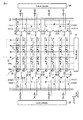
図3は、1個のセルアレイ1とその周辺回路の構成を示す回路図である。
FIG. 3 is a circuit diagram showing the configuration of one
図2のセルアレイ1−1,1−2は、例えば、図3の構成をそれぞれ有している。
セルアレイ1には、カラム方向に延在する複数のビット線BL、カラム方向に延在する複数のソース線SL、ロウ方向に延在する複数のワード線WL、及びロウ方向に延在する複数の参照ワード線RWLが、配設されている。
The cell arrays 1-1 and 1-2 in FIG. 2 have, for example, the configuration in FIG.
The
図3には、8本のビット線BL<0>〜BL<7>、8本のソース線SL<0>〜SL<7>、4本のワード線WL<0>〜WL<3>、2本の参照ワード線RWL<0>〜SL<1>が、例示されているが、これらの本数に限定されない。 FIG. 3 shows eight bit lines BL <0> to BL <7>, eight source lines SL <0> to SL <7>, four word lines WL <0> to WL <3>, Although two reference word lines RWL <0> to SL <1> are illustrated, the number is not limited to these numbers.
上述したように、セルアレイ1内には、メモリセル領域11及び参照セル領域12が設けられている。メモリセル領域11は、複数のメモリセルMCがマトリクス状に配列されている。参照セル領域12は、複数の参照セルRCが配列されている。
As described above, the memory cell region 11 and the reference cell region 12 are provided in the
メモリセルMCは、1個の抵抗変化型メモリ素子3と少なくとも1つのセルトランジスタ2とを含んでいる。セルトランジスタ2として、例えば、nチャネル型MOS(Metal Oxide Semiconductor)トランジスタが用いられる。抵抗変化型メモリ素子3の一端はビット線BL<m>に接続され、抵抗変化型メモリ素子3の他端はセルトランジスタ2の電流経路の一端に接続される。セルトランジスタ2の電流経路の他端はソース線SL<m>に接続され、セルトランジスタ2のゲートはワード線WL<n>に接続される。mは、0〜7のうち任意の整数である。nは、0〜3のうち任意の整数である。
The memory cell MC includes one resistance change
抵抗変化型メモリ素子3としては、例えば、磁気抵抗効果素子(例えば、MTJ素子)が用いられる。図4は、MTJ素子3の構成を示す断面図である。MTJ素子3は、下部電極38、参照層(固定層ともよばれる)31、非磁性層(トンネルバリア層ともよばれる)32、記録層(記憶層、自由層ともよばれる)33、上部電極39が、積層されて形成されている。尚、各層の積層順序は逆転していても構わない。
As the resistance change
参照層31及び記録層33のそれぞれは、強磁性材料から形成される。参照層31及び記録層33は、膜面に対して垂直な方向において磁気異方性を有し、それらの容易磁化方向は膜面に対して垂直である。尚、参照層31及び記録層33の磁化方向は、膜面に対して平行であってもよい。
Each of the
参照層31は、磁化(或いはスピン)の向きが不変である(固定されている)。記録層33は、磁化(或いはスピン)の向きが可変である(反転する)。
参照層31は、記録層33よりも十分大きな垂直磁気異方性エネルギーを持つように形成される。磁性層31,33の磁気異方性の設定は、材料構成や膜厚を調整することで可能である。MTJ素子3において、記録層33の磁化反転しきい値が小さくされ、参照層31の磁化反転しきい値を記録層33の磁化反転しきい値よりも大きくされる。これによって、磁化方向が不変な参照層31と磁化方向が可変な記録層33とを有するMTJ素子21を形成できる。
In the
The
図5は、MTJ素子3の磁化状態を説明する模式図である。本実施形態では、MTJ素子3に書き込み電流Iwを流し、この書き込み電流IwによってMTJ素子3の磁化状態を制御するスピン注入書き込み方式が、用いられる。書き込み電流Iwの大きさは、記録層33の磁化反転しきい値以上の電流値を有し、参照層31の磁化反転しきい値未満の電流値を有するように、制御される。
FIG. 5 is a schematic diagram for explaining the magnetization state of the
MTJ素子3は、参照層31と記録層33との磁化の相対関係が平行か反平行かによって、高抵抗状態と低抵抗状態との2つの状態のいずれかをとることができる。
The
図5に示すように、磁化配列が反平行状態のMTJ素子3に対して、記録層33から参照層31へ向かう書き込み電流Iwを流すと、参照層31の磁化配列と同じ向きのスピンを有する電子が、非磁性層32を介して記録層33に供給される電子として支配的になる。
As shown in FIG. 5, when a write current Iw from the
非磁性層32を通過した(トンネリングした)電子のスピントルクによって、記録層33の磁化の向きが、参照層33の磁化の向きと同じになるように、変化する(反転する)。これによって、参照層31と記録層33との磁化の相対関係が平行になる。
The magnetization direction of the
参照層31及び記録層33の磁化配列が平行状態である場合、MTJ素子3の抵抗値は最も低くなる、すなわち、MTJ素子3は低抵抗状態になる。MTJ素子21の低抵抗状態は、例えば、データ“0”と設定される。
When the magnetization arrangement of the
磁化配列が平行状態のMTJ素子3に対して、参照層33から記録層31へ向かう書き込み電流Iwを流すと、参照層31の磁化配列及び磁化が反転する前の記録層33の磁化配列と同じ向きのスピンを有する電子は、非磁性層32を介して参照層31に移動する。その一方で、参照層31の磁化配列と反対の向きのスピンを有する電子は、非磁性層32或いは参照層31によって反射される。反射された電子のスピントルクによって、記憶層33の磁化の向きが、参照層41の磁化配列と反対になるように、変化する。これによって、記録層32と参照層33との磁化の相対関係が反平行になる。
When the write current Iw from the
参照層31及び記録層33の磁化配列が平行状態である場合、MTJ素子3の抵抗値は最も高くなる、すなわち、MTJ素子3は高抵抗状態になる。MTJ素子3の高抵抗状態を、例えば、データ“1”と設定される。
When the magnetization arrangement of the
これにより、MTJ素子3が1ビットデータ(2値データ)を記憶可能な記憶素子として使用される。書き込み電流Iwは、書き込みデータに応じて、選択セルを経由してビット線側からソース線側へ、選択セルを経由してソース線側からソース線側へ流れるように、選択セル内のMTJ素子に3供給される。書き込み電流Iwは、電流源又は電圧源を有する書き込み回路(図示せず)によって、生成される。
Thereby, the
参照セルRCは、例えば、メモリセルMCと同じ回路構成を有し、1個の抵抗素子23と1個のセルトランジスタ24とを含んでいる。抵抗素子23の一端は、ビット線BL<m>に接続され、抵抗素子23の他端はセルトランジスタ24の電流経路の一端に接続され、セルトランジスタ24の電流経路の他端はソース線SL<m>に接続される。セルトランジスタ24のゲートは、参照ワード線RWLに接続される。このように、参照セルRCは、メモリセルMCと共通のビット線BL<m>及びソース線SL<m>に接続されている。
The reference cell RC has, for example, the same circuit configuration as that of the memory cell MC, and includes one
抵抗素子23は、選択セルからのデータ読み出し時、メモリセルMCのデータを判定する基準となる参照電流を生成するために使用され、その抵抗値は固定される。抵抗素子23は、例えば、MTJ素子3と同様の積層構造を有する。ただし、参照セルRCの抵抗素子23は、データの書き込み対象として選択されず、抵抗値が変化されないように参照セルRCに対する動作が制御される。あるいは、参照セルRCの抵抗素子23の記録層3の磁化が、参照層34と同様に固定されるように、形成されてもよい。
The
各ビット線BL<m>は、カラム選択セルトランジスタ27を介して4本のデータ線DL1のうちの1本に接続される。カラム選択トランジスタ27は、例えば、nチャネル型MOSトランジスタである。カラム選択トランジスタ27のゲートは、カラム選択線CSLD1に接続される。 Each bit line BL <m> is connected to one of the four data lines DL1 via the column selection cell transistor 27. The column selection transistor 27 is, for example, an n channel type MOS transistor. The gate of the column selection transistor 27 is connected to the column selection line CSLD1.
カラムデコーダ7Aは、バッファ(2個のインバータ)を介してカラム選択線CSLD1に接続される。カラムデコーダ7Aは、カラム選択線CSLD1を介してカラム選択トランジスタ28のオン/オフを制御する。カラム選択トランジスタ27がオンされることによって、選択されたビット線BL<m>が、データ線DL1に接続される。
The
各ビット線BL<m>には、電界効果トランジスタ28が接続される。トランジスタ28は、例えば、nチャネル型MOSトランジスタである。電界効果トランジスタ28のドレインはビット線BL<m>に接続され、電界効果トランジスタ28のゲートは制御線bCSLD1に接続され、電界効果トランジスタ28のソースは接地されている(電源Vssに接続される)。 A field effect transistor 28 is connected to each bit line BL <m>. The transistor 28 is an n-channel MOS transistor, for example. The drain of the field effect transistor 28 is connected to the bit line BL <m>, the gate of the field effect transistor 28 is connected to the control line bCSLD1, and the source of the field effect transistor 28 is grounded (connected to the power supply Vss). .
制御線bCSLD1は、1個のインバータを介して、カラムデコーダ7Aに接続され、制御線bCSLD1には、カラム選択線CSLD1の反転信号が供給される。トランジスタ28は、非選択ビット線BLを接地電圧Vssに設定する。これにより、選択ビット線BLに隣接するビット線は接地電圧Vssに設定されるため、安定した読み出し動作を実現できる。
The control line bCSLD1 is connected to the
各ソース線SL<m>は、カラム選択トランジスタ25を介して4本のデータ線DL2のうちの1本に接続される。カラム選択トランジスタ25のゲートは、カラム選択線CSLD2に接続される。
Each source line SL <m> is connected to one of the four data lines DL2 via the
カラムデコーダ7Bは、バッファ(2個のインバータ)を介してカラム選択線CSLD2に接続される。カラムデコーダ7Bは、カラム選択線CSLD2を介してカラム選択トランジスタ27のオン/オフを制御する。カラム選択トランジスタ25がオンされることによって、選択されたソース線SL<m>が、データ線DL2に接続される。
The
各ソース線SL<m>には、電界効果トランジスタ28が接続される。電界効果トランジスタ28のドレインはソース線SLに接続され、電界効果トランジスタ28のゲートは制御線bCSLD2に接続され、電界効果トランジスタ28のソースは接地されている。制御線bCSLD2は、1個のインバータを介してカラムデコーダ7Bに接続される。制御線bCSLD2には、カラム選択線CSLD2の反転信号が供給される。電界効果トランジスタ28は、非選択ソース線SLを接地電圧VSSに設定する。これにより、選択ソース線SLに隣接するソース線は接地電圧VSSに設定されるため、安定した読み出し動作を実現できる。
A field effect transistor 28 is connected to each source line SL <m>. The drain of the field effect transistor 28 is connected to the source line SL, the gate of the field effect transistor 28 is connected to the control line bCSLD2, and the source of the field effect transistor 28 is grounded. The control line bCSLD2 is connected to the
図6を用いて、読み出し動作時における各セルMC,RC、センスアンプ40A及び電流シンク40Bの接続関係について、説明する。
図6は、あるビット線BLとあるソース線SLとに接続されたメモリセルMCに対して読み出し動作が実行された場合における各構成の接続関係が模式的に示されている。
The connection relationship among the cells MC and RC, the
FIG. 6 schematically shows the connection relationship of each component when a read operation is performed on a memory cell MC connected to a certain bit line BL and a certain source line SL.
図6に示される例では、メモリセル(選択セル)MC_sが選択され、他のメモリセルは非選択である。選択セルMC_sが接続されたビット線BL及びソース線SLのことを、選択ビット線及び選択ソース線SLとそれぞれよぶ。 In the example shown in FIG. 6, the memory cell (selected cell) MC_s is selected, and the other memory cells are not selected. The bit line BL and the source line SL to which the selected cell MC_s is connected are referred to as a selected bit line and a selected source line SL, respectively.
読み出し動作時、選択ビット線BLには、nチャネル型電界効果トランジスタ(例えば、nチャネル型MOSトランジスタ)5N−1の電流経路の一端が接続される。nチャネル型MOSトランジスタ5N−1の電流経路の他端は、センスアンプ40Aの一方の入力端子に接続される。nチャネル型MOSトランジスタ5N−1のゲートには、制御電圧VCLMPnが印加される。この制御電圧VCLMPnが印加されることによって、nチャネル型MOSトランジスタ5N−1は、読み出し動作時において、ビット線BLの電位VBLをクランプ(実質的に一定に)する。
During a read operation, one end of a current path of an n-channel field effect transistor (for example, an n-channel MOS transistor) 5N-1 is connected to the selected bit line BL. The other end of the current path of n-
nチャネル型MOSトランジスタ5N−1のしきい値電圧Vtnは、例えば、0.2V(絶対値)程度である。
The threshold voltage Vtn of the n-
読み出し動作時、選択ソース線SLには、pチャネル型電界効果トランジスタ(例えば、pチャネル型MOSトランジスタ)5P−1の電流経路の一端が接続される。pチャネル型MOSトランジスタ5P−1の電流経路の他端は、電流シンク40Bの一方の入力端子に接続される。pチャネル型MOSトランジスタ5P−1のゲートには、制御電圧VCLMPpが印加される。この制御電圧VCLMPpが印加されることによって、pチャネル型MOSトランジスタ5P−1は、読み出し動作時において、ソース線SLの電位VSLをクランプする。
During a read operation, one end of a current path of a p-channel field effect transistor (for example, a p-channel MOS transistor) 5P-1 is connected to the selected source line SL. The other end of the current path of p channel
pチャネル型MOトランジスタ5P−1のしきい値電圧Vtpは、例えば、0.2V(絶対値)程度である。
The threshold voltage Vtp of the p-channel
以下では、クランプ用の電界効果トランジスタ5N−1,5P−1のことを、クランプトランジスタ5N−1,5P−1とよぶ。また、制御電圧VCLMPn,VCLMPpのことを、クランプ電圧VCLMPn,VCLMPpとよぶ。
Hereinafter, the
このように、本実施形態のMRAMは、読み出し電流Irが流れる電流経路において、ビット線BLの電位をクランプするnチャネル型クランプトランジスタ5N−1が、複数のメモリセルが接続されたビット線BLに接続され、ソース線SLの電位をクランプするpチャネル型クランプトランジスタ5P−1が、ビット線BLと対になるソース線SLに接続されている。そして、ソース線SLの電位は、非選択のメモリセルが接続されたワード線WLの電位VWL_usより高く設定される。
As described above, in the MRAM of the present embodiment, the n-
図6において、図示の簡略化のために、nチャネル型/pチャネル型クランプトランジスタ5N−1,5P−1が、ビット線BL及びソース線SLにそれぞれ直接接続されている。しかし、クランプトランジスタ5N−1,5P−1は、その電流経路(チャネル)が読み出し回路(センスアンプ及び電流シンク)とビット線/ソース線との間に直列になるように接続され、かつ、ビット線/ソース線の電位をクランプできるように形成されていれば、データ線DL1,DL2や他の構成要素を介して、読み出し回路及びビット線/ソース線にそれぞれ接続されていてもよい。
In FIG. 6, n-channel / p-
参照セルを用いたデータ読み出し方式が用いられる場合、参照セルRCは、電界効果トランジスタ5N−2,5P−2を介して、読み出し回路(センスアンプ及び電流シンク)に電気的に接続される。
When the data read method using the reference cell is used, the reference cell RC is electrically connected to the read circuit (sense amplifier and current sink) via the
参照セルRCが接続されたビット線BL’には、nチャネル型MOSトランジスタ5N−2の電流経路の一端が接続されている。nチャネル型MOSトランジスタ5N−2の電流経路の他端は、センスアンプ40Aの他方の入力端子に接続される。
参照セルRCが接続されたソース線SL’には、pチャネル型MOSトランジスタ5P−2の電流経路の一端が接続されている。pチャネル型MOSトランジスタ5P−2の電流経路の他端は、電流シンク40Bに接続される。
One end of the current path of the n-
One end of the current path of the p-
以下では、説明の明確化のため、参照セルRCが接続されたビット線BL’のことを、参照ビット線BL’とよび、参照セルRCが接続されたソース線SL’のことを、参照ソース線SL’とよぶ。尚、MOSトランジスタ5N−2,5P−2も、データ線DL1,DL2のような他の構成要素を介して、読み出し回路40A,40B及び参照ビット線BL’/参照ソース線SL’にそれぞれ接続されてもよい。また、図3に示されるように、参照ビット線BL’及び参照ソース線SL’間にメモリセルが接続されているのは、もちろんである。
Hereinafter, for the sake of clarity, the bit line BL ′ to which the reference cell RC is connected is referred to as the reference bit line BL ′, and the source line SL ′ to which the reference cell RC is connected is referred to as the reference source. Call it line SL '. The
nチャネル型MOSトランジスタ5N−2のゲートには、制御信号VREFnが印加される。この制御信号VREFnが印加されることによって、nチャネル型MOSトランジスタ5N−2は、参照ビット線BL’の電位VBL’をクランプする。nチャネル型MOSトランジスタ5N−2のしきい値電圧は、例えば、nチャネル型クランプトランジスタ5N−1のしきい値電圧Vtnと同じ大きさである。
A control signal VREFn is applied to the gate of the n-
pチャネル型MOSトランジスタ5P−2のゲートには、制御電圧VREFpが印加される。この制御電圧VREFpが印加されることによって、pチャネル型MOSトランジスタ5P−2は、参照ソース線SL’の電位VSL’をクランプする。pチャネル型MOSトランジスタ5P−2のしきい値電圧は、例えば、pチャネル型クランプトランジスタ5P−1のしきい値電圧Vtpと同じ大きさである。
A control voltage VREFp is applied to the gate of the p-
参照ビット線BL’及び参照ソース線SL’に接続されたトランジスタ5N−2,5P−2は、クランプトランジスタ5N−1,5P−1と実質的に同様の機能を有し、参照ビット線BL’及び参照ソース線SL’の電位VBL’,VSL’を、読み出し動作時において、クランプする。
The
参照ビット線BL’及び参照ソース線SL’に対する制御電圧VREFn,VREFpの大きさは、例えば、クランプ電圧VCLMPn,VCLMPpの大きさと異なる。参照ビット線BL’及び参照ソース線SL’にそれぞれ接続されたMOSトランジスタ5N−2,5P−2は、クランプ電圧VCLMPn,VCLMPpと異なる大きさの制御電圧VREFn,VREFpが印加されることによって、参照ビット線BL’及び参照ソース線SL’の電位をそれぞれ制御する。
The magnitudes of the control voltages VREFn and VREFp for the reference bit line BL 'and the reference source line SL' are different from the magnitudes of the clamp voltages VCLMPn and VCLMPp, for example. The
尚、読み出し動作時、参照セルRCを経由して参照電流をセンスアンプ40Aに供給せずに、定電流源(又は定電圧源)が生成する一定の電流値を有する電流が、センスアンプ40Aに直接供給されてもよい。この場合、センスアンプ40Aの他方の入力端子は、参照セルに接続されずに、定電流源に接続される。
During a read operation, a current having a constant current value generated by a constant current source (or a constant voltage source) is supplied to the
データ読み出し時、選択ワード線WLに、例えば、1.2V程度の選択ワード線電位VWL_sが印加される。選択ワード電位VWL_sが、選択セルMC_s内のセルトランジスタ2sのゲートに印加され、セルトランジスタ2sがオンする。
一方、非選択ワード線には、例えば、0Vの電位が、非選択ワード線電位VWL_usとして印加される。非選択セルMC_us内のセルトランジスタ2usは、オフ状態が維持される。
At the time of data reading, a selected word line potential VWL_s of about 1.2 V, for example, is applied to the selected word line WL. The selected word potential VWL_s is applied to the gate of the
On the other hand, for example, a potential of 0 V is applied to the unselected word line as the unselected word line potential VWL_us. The cell transistor 2us in the non-selected cell MC_us is kept off.
尚、非選択セルMC_us内のセルトランジスタ2usがオフ状態であれば、非選択ワード線電位VWL_usは0Vより大きくともよい。但し、本実施形態において、非選択ワード線電位VWL_usは、ソース線電位VSLよりも小さいことが必要である。 If the cell transistor 2us in the non-selected cell MC_us is in an off state, the non-selected word line potential VWL_us may be larger than 0V. However, in this embodiment, the unselected word line potential VWL_us needs to be smaller than the source line potential VSL.
データ読み出し時、選択ビット線BLの電位VBLは、クランプトランジスタ5N−1による電位制御によって、“VCLMPn−Vtn”程度に設定され、選択ソース線SLの電位VSLは、クランプトランジスタ5P−1による電位制御によって、“VCLMPp+Vtp”程度に設定される。
At the time of data reading, the potential VBL of the selected bit line BL is set to about “VCLMPn−Vtn” by the potential control by the
選択ビット線BLの電位VBLが、選択ソース線SLの電位VSLより高くなるように、クランプ電圧VCLMPn,VCLMPpの大きさがそれぞれ調整されている。例えば、選択ビット線BLに対するクランプ電圧VCLMPnは、0.85V程度に設定され、選択ソース線SLに対するクランプ電圧VCLMPpは、例えば、0.35V程度に設定される。この場合、ビット線電位VBLは0.65V程度になり、ソース線電位VSLは0.55V程度になる。
それゆえ、読み出し電流Irは、選択セルMC_sを経由して、選択ビット線側から選択ソース線側に流れる。尚、クランプ電圧VCLMPn,VCLMPpの大きさは、上述の値に限定されない。また、上述のしきい値電圧Vtn,Vtpの大きさは、上述の値に限定されない。
The magnitudes of the clamp voltages VCLMPn and VCLMPp are adjusted so that the potential VBL of the selected bit line BL becomes higher than the potential VSL of the selected source line SL. For example, the clamp voltage VCLMPn for the selected bit line BL is set to about 0.85V, and the clamp voltage VCLMPp for the selected source line SL is set to about 0.35V, for example. In this case, the bit line potential VBL is about 0.65V, and the source line potential VSL is about 0.55V.
Therefore, the read current Ir flows from the selected bit line side to the selected source line side via the selected cell MC_s. Note that the magnitudes of the clamp voltages VCLMPn and VCLMPp are not limited to the above values. The magnitudes of the threshold voltages Vtn and Vtp are not limited to the above values.
また、データ読み出し時、参照ワード線RWLに、例えば、1.2V程度の選択ワード線電位VWL_rが印加される。選択ワード電位VWL_rが、参照セルRC内のセルトランジスタ24のゲートに印加され、セルトランジスタ24がオンされる。
At the time of data reading, a selected word line potential VWL_r of about 1.2 V, for example, is applied to the reference word line RWL. The selected word potential VWL_r is applied to the gate of the
参照ビット線BL’及び参照ソース線SL’に接続されたメモリセルにおいて、それらのメモリセル内のセルトランジスタがオフされる。即ち、参照ビット線BL’及び参照ソース線SL’に接続されたメモリセルに対して、0Vのワード線電位が、セルトランジスタのゲートに印加される。 In the memory cells connected to the reference bit line BL 'and the reference source line SL', the cell transistors in those memory cells are turned off. That is, for the memory cells connected to the reference bit line BL 'and the reference source line SL', a word line potential of 0 V is applied to the gate of the cell transistor.
参照ビット線BL’の電位VBL’は、電界効果トランジスタ5N−2による電位制御によって、“VREFn−Vtn”程度に設定される。参照ソース線SL’の電位VSL’は、電界効果トランジスタ5P−2による電位制御によって、“VREFp+Vtp”程度に設定される。参照ビット線BL’の電位VBL’は、参照ソース線SL’の電位VSL’より大きくなる。それゆえ、参照セルRCを流れる基準電流(参照電流)Irefは、参照ビット線側から参照ソース線側に流れる。
The potential VBL 'of the reference bit line BL' is set to about "VREFn-Vtn" by the potential control by the
尚、参照電流Irefの電流値は、MTJ素子が高抵抗状態のときに流れる読み出し電流の大きさとMTJ素子が低抵抗状態のときに流れる読み出し電流の大きさとの間になるように、制御電圧VREFn,VREFpとによって、調整される。 The current value of the reference current Iref is a control voltage VREFn so that it is between the magnitude of the read current that flows when the MTJ element is in the high resistance state and the magnitude of the read current that flows when the MTJ element is in the low resistance state. , VREFp.
読み出し時において、読み出し電流Irは、選択セルMC_sを経由して、センスアンプ40Aから電流シンク40Bに向かって流れる。また、参照電流Irefは、参照セルRCを経由して、センスアンプ40Aから電流シンク40Bに向かって流れる。
At the time of reading, the read current Ir flows from the
電流シンク40Bは、読み出し電流Ir及び参照電流Irefを引き込む。
The
センスアンプ40Aは、読み出し電流Irの大きさと参照電流Irefの大きさとを比較することによって、選択セルMC_s内のMTJ素子3sの抵抗状態(抵抗値)を検出する。検出されたMTJ素子3sの抵抗状態に基づいて、MTJ素子3sが記憶しているデータが、判別される。
The
参照セルRCを流れる電流Irefがデータ読み出し時における抵抗状態の検出(データ判別)のための基準電流として用いられることよって、動作に対する配線遅延の影響を緩和でき、データの読み出しが一定の電流(又は電位)を基準電流として実行される場合に比較して、読み出し動作の高速化が可能になる。 The current Iref flowing through the reference cell RC is used as a reference current for resistance state detection (data discrimination) at the time of data reading, so that the influence of the wiring delay on the operation can be alleviated, and the data reading is a constant current (or Compared with the case where the operation is performed using the potential as a reference current, the reading operation can be performed at a higher speed.
このように、読み出し動作時、選択セルMC_sのセルトランジスタ2sがオン状態になり、選択セルMC_s内を、読み出し電流Irが流れる。このとき、非選択セルMC_usのセルトランジスタ2_usはオフ状態であり、非選択ワード線WLの電位VWL_usよりも、ソース線電位VSLが高くなっている。
Thus, during the read operation, the
すなわち、本実施形態のMRAMにおいて、選択セルMC_sに対するデータ読み出し時、非選択セルMC_us内のセルトランジスタ2_usのゲート電圧よりも、非選択セルMC_us内のセルトランジスタ2_usのソース電圧の方が高くなっている。この場合、nチャネル型のセルトランジスタ2_usのチャネル(p型半導体層)−ソース(n型半導体層)間には、逆バイアスが印加される。 That is, in the MRAM of this embodiment, when reading data from the selected cell MC_s, the source voltage of the cell transistor 2_us in the non-selected cell MC_us is higher than the gate voltage of the cell transistor 2_us in the non-selected cell MC_us. Yes. In this case, a reverse bias is applied between the channel (p-type semiconductor layer) and the source (n-type semiconductor layer) of the n-channel cell transistor 2_us.
それゆえ、非選択セルMC_s内のセルトランジスタ2usからのリーク電流は、低減される。セルトランジスタのリーク電流は、例えば、短チャネル効果のような、素子の微細化の悪影響に起因する。 Therefore, the leakage current from the cell transistor 2us in the non-selected cell MC_s is reduced. The leak current of the cell transistor is caused by an adverse effect of element miniaturization such as a short channel effect.
また、参照ビット線BL’及び参照ソース線SL’に接続されたメモリセル(非選択セル)においても、セルトランジスタのゲート電圧(ワード線電位)がソース電圧よりも高い。それゆえ、参照ビット線BL’及び参照ソース線SL’間の複数のメモリセルにおいても、メモリセルからのリーク電流は低減する。 Also in the memory cells (non-selected cells) connected to the reference bit line BL ′ and the reference source line SL ′, the gate voltage (word line potential) of the cell transistor is higher than the source voltage. Therefore, even in a plurality of memory cells between the reference bit line BL 'and the reference source line SL', the leakage current from the memory cell is reduced.
したがって、第1の実施形態の抵抗変化型メモリは、データ読み出し時における非選択セルからのリーク電流を低減でき、そのリーク電流がデータ読み出しに対して大きなノイズとなるのを抑制できる。 Therefore, the resistance change type memory according to the first embodiment can reduce the leakage current from the non-selected cells at the time of data reading, and can suppress the leakage current from becoming a large noise for the data reading.
以上のように、第1の実施形態によれば、データの読み出しの精度を向上できる。 As described above, according to the first embodiment, the accuracy of reading data can be improved.
(b) 動作
図2及び図6を用いて、第1の実施形態の抵抗変化型メモリ(例えば、MRAM)の動作について、説明する。ここでは、本実施形態のMRAMの読み出し動作について説明する。
(B) Operation
The operation of the resistance change type memory (for example, MRAM) of the first embodiment will be described with reference to FIGS. Here, the read operation of the MRAM of this embodiment will be described.
データ読み出し時、外部からMRAMチップ内に、読み出しコマンド及び読み出し対象のアドレスが入力される。 When reading data, a read command and a read target address are input from the outside into the MRAM chip.
図2のロウデコーダ8−1,8−2は、入力されたアドレス信号に基づいて、複数のワード線の中から1本のワード線を選択する。図2のカラムデコーダ7A−1,7A−2,7B−1,7B−3は、入力されたアドレスに基づいて、カラム選択トランジスタ25,27のオン/オフを制御する。そして、カラムデコーダ7A−1,7A−2,7B−1,7B−3は、複数のビット線の中から1本のビット線を選択し、複数のソース線の中から1つのソース線を選択する。
The row decoders 8-1 and 8-2 in FIG. 2 select one word line from a plurality of word lines based on the input address signal. The column decoders 7A-1, 7A-2, 7B-1, and 7B-3 in FIG. 2 control the on / off of the
参照セルRCを用いたデータ読み出し方式において、読み出し時には、セルアレイ1−1のメモリセルMCが選択されると、セルアレイ1−2の参照セルRCが選択される。これとは反対に、セルアレイ1−2内のメモリセルMCが選択されると、セルアレイ1−1内の参照セルRCが選択される。 In the data read method using the reference cell RC, at the time of reading, when the memory cell MC of the cell array 1-1 is selected, the reference cell RC of the cell array 1-2 is selected. On the contrary, when the memory cell MC in the cell array 1-2 is selected, the reference cell RC in the cell array 1-1 is selected.
例えば、図2に示されるように、セルアレイ1−1内において、同じ選択ワード線に接続された2つのメモリセルMC1,MC2から同時にデータを読み出すこともできる。
メモリセルMC1,MC2は、異なるカラムに属し、互いに異なるビット線BL及びソース線SLに接続されている。セルアレイ1−1内のメモリセルMC1,MC2が同時に選択された場合、セルアレイ1−2内の2つの参照セルRC1,RC2が同時に選択される。メモリセルMC1及びメモリセルMC2は、共通のワード線WLに選択されている。2つの参照セルRC1,RC2は、異なるカラムに属し、互いに異なるビット線BL及びソース線SLに接続されている。2つの参照セルRC1,RC2は、共通の参照ワード線RWLに接続されている。
For example, as shown in FIG. 2, data can be read simultaneously from two memory cells MC1 and MC2 connected to the same selected word line in the cell array 1-1.
The memory cells MC1 and MC2 belong to different columns and are connected to different bit lines BL and source lines SL. When the memory cells MC1 and MC2 in the cell array 1-1 are simultaneously selected, the two reference cells RC1 and RC2 in the cell array 1-2 are simultaneously selected. The memory cell MC1 and the memory cell MC2 are selected as a common word line WL. The two reference cells RC1 and RC2 belong to different columns and are connected to different bit lines BL and source lines SL. The two reference cells RC1, RC2 are connected to a common reference word line RWL.
センスアンプ40A−1が、データ線DL1を介してメモリセルMC1及び参照セルRC1に接続され、電流シンク40B−1が、データ線DL2を介してメモリセルMC1及び参照セルRC1に接続される。センスアンプ40A−2が、データ線DL1を介してメモリセルMC2及び参照セルRC2に接続され、電流シンク40B−2が、データ線DL2を介してメモリセルMC2及び参照セルRC2に接続される。
The
センスアンプ40A−1は、メモリセルMC1を経由して電流シンク40B−1に流れる読み出し電流の大きさを、センスアンプ40A−1から参照セルRC1を経由して、電流シンク40B−1に流れる参照電流の大きさを比較し、メモリセルMC1内の抵抗変化型メモリ素子(MTJ素子)の抵抗状態を検出する。検出された抵抗状態に基づいて、MTJ素子が記憶するデータが判別される。メモリセルMC1に対するデータの読み出しと同じ動作サイクルにおいて、センスアンプ40A−2が、メモリセルMC2からの読み出し電流と参照セルRC2からの参照電流とを比較することによって、メモリセルMC2のデータが判別される。
The
このように、本実施形態のMRAMは、2つのメモリセルMC1,MC2から同時にデータを読み出すことができる。 As described above, the MRAM of this embodiment can simultaneously read data from the two memory cells MC1 and MC2.
図6を用いて、選択セルに対するデータ読み出し時におけるビット線及びソース線の電位の関係について、説明する。 The relationship between the potentials of the bit line and the source line at the time of reading data from the selected cell will be described with reference to FIG.
図6に示されるように、選択ワード線WLには、選択セルMC_s内のセルトランジスタ2sがオンするように、1.2V程度の選択ワード線電位VWL_sが印加される。非選択ワード線には、例えば、0V程度の非選択ワード線電位VWL_usが印加される。
As shown in FIG. 6, a selected word line potential VWL_s of about 1.2 V is applied to the selected word line WL so that the
データ読み出し時において、クランプトランジスタ5N−1は、選択ビット線BLの電位VBLを制御する。クランプトランジスタ5N−1のゲートにクランプ電圧VCLMPnが印加される。選択ビット線BLの電位VBLは、クランプ電圧VCLMPnの大きさに応じて、nチャネル型クランプトランジスタ5N−1によってクランプされる。nチャネル型クランプトランジスタ5N−1のしきい値電圧が“Vtn”で示される場合、選択ビット線BLの電位VBLは、“VCLMPn−Vtn”で示される。
At the time of data reading, the
クランプトランジスタ5P−1は、選択ソース線SLの電位VSLを制御する。クランプトランジスタ5P−1のゲートにクランプ電圧VCLMPpが印加される。選択ソース線SLの電位VSLは、クランプ電圧VCLMPpの大きさに応じて、pチャネル型クランプトランジスタ5P−1によってクランプされる。pチャネル型クランプトランジスタ5P−1のしきい値電圧が“Vtp”で示される場合、選択ソース線SLの電位VSLは、“VCLMPp+Vtp”で示される。
The
ここで、クランプ電圧VCLMPnが0.85V程度、しきい値電圧Vtnが0.2V程度である場合、選択ビット線電位VBLは、0.65V程度になる。また、クランプ電圧VCLMPpが0.35V程度、しきい値電圧Vtpが0.2V程度である場合、選択ソース線電位VSLは、0.55V程度になる。尚、クランプ電圧VCLMPn,VCLMPpの大きさは、この値に限定されない。また、クランプトランジスタ5N,5Pのしきい値電圧Vtn,Vtpは、形成されるトランジスタ5N,5Pの特性に応じる。
Here, when the clamp voltage VCLMPn is about 0.85V and the threshold voltage Vtn is about 0.2V, the selected bit line potential VBL is about 0.65V. When the clamp voltage VCLMPp is about 0.35V and the threshold voltage Vtp is about 0.2V, the selected source line potential VSL is about 0.55V. The magnitudes of the clamp voltages VCLMPn and VCLMPp are not limited to these values. The threshold voltages Vtn and Vtp of the
参照セルRCが接続された参照ワード線RWLに、参照セルRC内のセルトランジスタ24がオンするように、例えば、1.2V程度の電位VWL_rが印加される。参照ビット線BL’及び参照ソース線SL’間に接続されたメモリセルにおいて、それらのメモリセル内のセルトランジスタのゲートには、0Vのワード線電位(非選択ワード線電位)が印加される。それゆえ、参照ビット線及び参照ソース線間のメモリセル内のセルトランジスタは、オフしている。
For example, a potential VWL_r of about 1.2 V is applied to the reference word line RWL to which the reference cell RC is connected so that the
参照セルRCが接続された参照ビット線BL’の電位VBL’は、nチャネル型MOSトランジスタ5N−2によって、制御される。nチャネル型MOSトランジスタ5N−2のゲートに、制御電圧VREFnが印加され、制御電圧VREFnの大きさに応じ、参照ビット線BL’の電位VBL’がクランプされる。参照セルRCが接続された参照ソース線SL’の電位VSL’は、pチャネル型MOSトランジスタ5P−2によって制御される。pチャネル型MOSトランジスタ5P−2のゲートに、制御電圧VREFpが印加され、制御電圧VREFpの大きさに応じて、参照ソース線SL’の電位VSL’がクランプされる。
The potential VBL 'of the reference bit line BL' to which the reference cell RC is connected is controlled by the n-
nチャネル型MOSトランジスタ5N−2のしきい値電圧が“Vtn”で示される場合、参照ビット線BLの電位VBL’は、例えば、“VREFn−Vtn”で示される。pチャネル型MOSトランジスタ5P−2のしきい値電圧が“Vtp”で示される場合、参照ソース線BLの電位VSL’は、例えば、“VREFp+Vtp”で示される。尚、制御電圧VREFn,VREFpの大きさは、クランプ電圧VCLMPn,VCLMPpの大きさと同じでもよいし、異なる大きさであってもよい。但し、参照ビット線BL’の電位VBL’が、参照ソース線SL’の電位VSL’より大きくなるように調整される。
When the threshold voltage of the n-
尚、参照電流Irefの電流値は、MTJ素子が高抵抗状態のときに流れる読み出し電流の大きさとMTJ素子が低抵抗状態のときに流れる読み出し電流の大きさとの間になるように、制御電圧VREFn,VREFpとによって、調整される。 The current value of the reference current Iref is a control voltage VREFn so that it is between the magnitude of the read current that flows when the MTJ element is in the high resistance state and the magnitude of the read current that flows when the MTJ element is in the low resistance state. , VREFp.
選択ビット線BLと選択ソース線SLとの間の電位差は、0.1V程度である。この電位差によって、読み出し電流Irが、オン状態のセルトランジスタ2sを経由して、選択セルMC_s内のMTJ素子3sを流れる。また、参照ビット線BL’と参照ソース線SL’との電位差によって、参照電流Irefが、オン状態のセルトランジスタ24を経由して、参照セルRC内の抵抗素子23を流れる。
The potential difference between the selected bit line BL and the selected source line SL is about 0.1V. Due to this potential difference, the read current Ir flows through the
上述のように、センスアンプ40Aは、読み出し電流Irと参照電流Irefとを比較する。これによって、選択セルMC_s内のMTJ素子3sの抵抗状態(抵抗値)が検出され、MTJ素子3sが記憶しているデータが読み出される。
As described above, the
ここで、上述の非選択ワード線VWL_us及び選択ソース線VSLとの電位の関係により、非選択セルMC_us内のセルトランジスタ2usにおいて、そのセルトランジスタ2usのゲートには0Vが印加され、セルトランジスタ2usのソースには、0.55Vが印加される。つまり、nチャネル型のセルトランジスタ2usにおいて、チャネル−ソース間(pn接合)に逆バイアスが印加される。このため、非選択セル2usのリーク電流は低減され、読み出し時のノイズが低減する。 Here, due to the potential relationship between the unselected word line VWL_us and the selected source line VSL, 0 V is applied to the gate of the cell transistor 2us in the cell transistor 2us in the unselected cell MC_us. 0.55V is applied to the source. That is, in the n-channel cell transistor 2us, a reverse bias is applied between the channel and the source (pn junction). For this reason, the leakage current of the non-selected cell 2us is reduced, and noise during reading is reduced.
また、参照ビット線BL’及び参照ソース線SL’間に接続されたメモリセルのセルトランジスタに対しても、参照ソース線SL’の電位VSL’が、ワード線電位(非選択ワード線電位)よりも高くなっている。それゆえ、参照ビット線BL’及び参照ソース線SL’間のメモリセル内のセルトランジスタのリーク電流も、低減する。 Further, for the cell transistor of the memory cell connected between the reference bit line BL ′ and the reference source line SL ′, the potential VSL ′ of the reference source line SL ′ is higher than the word line potential (non-selected word line potential). Is also high. Therefore, the leakage current of the cell transistor in the memory cell between the reference bit line BL ′ and the reference source line SL ′ is also reduced.
尚、本実施形態において、参照セルRCを流れる電流Irefが、基準電流として、センスアンプ40Aに供給される。しかし、読み出し動作時、センスアンプ40Aに参照セルRCが接続されずに、定電流源(又は定電圧源)からの一定の電流が基準電流として、センスアンプ40Aに直接供給されてもよい。
In the present embodiment, the current Iref flowing through the reference cell RC is supplied to the
以上のように、第1の実施形態の抵抗変化型メモリの動作によれば、データの読み出しの精度を向上した抵抗変化型メモリを提供できる。 As described above, according to the operation of the resistance change memory according to the first embodiment, it is possible to provide a resistance change memory with improved data reading accuracy.
(2) 第2の実施形態
図7及び図8を参照して、第2の実施形態の抵抗変化型メモリについて、説明する。尚、以下では、第2の実施形態と第1の実施形態のとの相違点について、主に説明し、重複する説明については、必要に応じて行う。
(2) Second embodiment
The resistance change type memory according to the second embodiment will be described with reference to FIGS. In the following, differences between the second embodiment and the first embodiment will be mainly described, and overlapping descriptions will be given as necessary.
図7及び図8を用いて、第2の実施形態の抵抗変化型メモリ(例えば、MRAM)の回路構成について説明する。 The circuit configuration of the resistance change type memory (for example, MRAM) of the second embodiment will be described with reference to FIGS.
図7に示されるように、読み出し回路として、電流ソース41A−1,41A−2とセンスアンプ41B−1,41B−2とが用いられてもよい。
As illustrated in FIG. 7,
電流ソース41A−1,41A−2は、データ線DL1に接続される。電流ソース41A−1,41A−2は、データ線DL1及びビット線BLに対して、電流を出力する。
センスアンプ41B−1,41B−2は、データ線DL2に接続される。センスアンプ41B−1,41B−2は、選択セルを流れた読み出し電流Irと基準電流とを比較する。
The
データ読み出し時、例えば、電流ソース41A−1は、データ線DL1を介して、セルアレイ1−1内のメモリセルMC1とセルアレイ1−2内の参照セルRC1に接続される。電流ソース41A−2は、データ線DL1を介して、セルアレイ1−1内のメモリセルMC2とセルアレイ1−2内の参照セルRC2に接続される。
At the time of data reading, for example, the
センスアンプ41B−1は、データ線DL2を介して、セルアレイ1−1内のメモリセルMC1とセルアレイ1−2内の参照セルRC1とに接続される。センスアンプ41B−2は、データ線DL2を介して、セルアレイ1−1内のメモリセルMC2とセルアレイ1−2内の参照セルRC2とに接続される。
The
これによって、第1の実施形態と同様に、1回のデータ読み出しの動作サイクルにおいて、2個のメモリセルMC1,MC2から同時にデータを読み出すことができる。 As a result, as in the first embodiment, data can be simultaneously read from the two memory cells MC1 and MC2 in one data read operation cycle.
尚、電流ソース/センスアンプ41A−1,41A−2,41B−1,41B−2とセルアレイ1−1,1−2内のメモリセル/参照セルとの接続関係は、入力されたコマンド及びアドレスに応じたカラムデコーダ7A−1,7A−2,7B−1,7B−2の制御によって、変更可能である。
The connection relationship between the current source /
第2の実施形態のMRAMにおいて、電流ソース41A−1,41A−2が高電位側の読み出し回路として機能し、センスアンプ41B−1,41B−2が低電位側の読み出し回路として機能する。
In the MRAM of the second embodiment, the
本実施形態において、第1の実施形態と同様に、読み出し動作時に、選択ビット線及び選択ソース線の電位をクランプするトランジスタ5N,5Pが、設けられている。
In the present embodiment, as in the first embodiment,
図8に示されるように、nチャネル型クランプランジスタ5N−1の電流経路の一端は、電流ソース41Aに接続され、nチャネル型クランプランジスタ5N−1の電流経路の一端は、ビット線BLに接続されている。pチャネル型クランプトランジスタ5P−1の電流経路の一端は、センスアンプ41Bの一方の入力端子に接続され、pチャネル型クランプトランジスタ5P−1の電流経路の他端は、ソース線SLに接続されている。
As shown in FIG. 8, one end of the current path of the n-
このように、第2の実施形態においても、読み出し電流Irが流れる電流経路において、ビット線BLの電位をクランプするnチャネル型クランプトランジスタ5N−1の電流経路(チャネル)が、複数のメモリセルが接続されたビット線BLに直列に接続され、ソース線SLの電位をクランプするpチャネル型クランプトランジスタ5P−1の電流経路(チャネル)が、ビット線BLと対になるソース線SLに接続されている。
As described above, also in the second embodiment, in the current path through which the read current Ir flows, the current path (channel) of the n-
nチャネル型トランジスタ5N−2の電流経路の一端は、電流ソース41Aに接続され、nチャネル型トランジスタ5N−2の電流経路の他端は、参照ビット線BL’に接続されている。pチャネル型MOSトランジスタ5P−2の電流経路の一端は、センスアンプ41Bの他方の入力端子に接続され、pチャネル型MOSトランジスタ5P−2の電流経路の他端は、参照ソース線SL’に接続される。
One end of the current path of the n-
読み出し時において、読み出し電流Irは、選択セルMC_sを経由して、電流ソース41Aからセンスアンプ41Bに向かって流れる。参照電裕Irefは参照セルRCを経由して、電流ソース41Aからセンスアンプ41Bに向かって流れる。
At the time of reading, the read current Ir flows from the
そして、センスアンプ41Bは、供給された読み出し電流Irと参照電流Irefとを比較する。これによって、選択セルMC_s内のMTJ素子3sの抵抗状態が検出され、MTJ素子3sが記憶しているデータが判別される。
Then, the
第2の実施形態のMRAMにおいても、第1の実施形態と同様に、クランプ電圧VCLMPn,VCLMPpによって、選択ビット線電位VBLは、選択ソース線電位VSLより高くなるように、制御される。 In the MRAM of the second embodiment, similarly to the first embodiment, the selected bit line potential VBL is controlled to be higher than the selected source line potential VSL by the clamp voltages VCLMPn and VCLMPp.
選択ワード線電位VWL_sは、選択ビット線電位VBLより大きく、選択ソース線電位VSLより大きい。また、選択ソース線電位VSLは、非選択ワード線電位VWL_usより大きい。 The selected word line potential VWL_s is higher than the selected bit line potential VBL and higher than the selected source line potential VSL. The selected source line potential VSL is higher than the unselected word line potential VWL_us.
それゆえ、本実施形態においても、非選択セルMC_us内のセルトランジスタ2_usのゲート電圧は、そのセルトランジスタ2_usのソース電圧より小さい。それゆえ、セルトランジスタ2_usのチャネル−ソース(pn接合)間に、逆バイアスが印加され、非選択セルMC_usからのリーク電流は低減される。この結果として、読み出し時に、リーク電流に起因するノイズが低減する。 Therefore, also in this embodiment, the gate voltage of the cell transistor 2_us in the non-selected cell MC_us is lower than the source voltage of the cell transistor 2_us. Therefore, a reverse bias is applied between the channel and source (pn junction) of the cell transistor 2_us, and the leakage current from the unselected cell MC_us is reduced. As a result, noise due to leakage current is reduced during reading.
したがって、第2の実施形態の抵抗変化型メモリは、第1の実施形態の抵抗変化型メモリと同様に、データの読み出しの精度を向上できる。 Therefore, the resistance change type memory according to the second embodiment can improve the accuracy of data reading, similar to the resistance change type memory according to the first embodiment.
(3) 変形例
図9及び図10を参照して、第1及び第2の実施形態に係る抵抗変化メモリの変形例について、説明する。
(3) Modification
A modification of the resistance change memory according to the first and second embodiments will be described with reference to FIGS.
第1及び第2の実施形態において、MRAMが抵抗変化型メモリの一例として例示されている。但し、抵抗変化型メモリは、例えば、ReRAM(Resistive RAM)やPCRAM(Phase Change RAM)のような、MRAM以外の抵抗変化型メモリでもよいのはもちろんである。 In the first and second embodiments, the MRAM is exemplified as an example of the resistance change type memory. However, the resistance change type memory may of course be a resistance change type memory other than MRAM, such as ReRAM (Resistive RAM) and PCRAM (Phase Change RAM).
例えば、ReRAMにおいて、メモリ素子に、可変抵抗素子が用いられる。ReRAMに用いられるメモリ素子は、電圧、電流又は熱などのエネルギーによって、素子の抵抗値が可逆的に変化し、抵抗値が変化した状態を不揮発に保持する。 For example, in a ReRAM, a variable resistance element is used as a memory element. A memory element used in ReRAM reversibly changes the resistance value of the element by energy such as voltage, current, or heat, and holds the state in which the resistance value has changed in a nonvolatile manner.
図9は、ReRAMに用いられる抵抗変化型メモリ素子(可変抵抗素子)3の構造例を示している。 FIG. 9 shows a structural example of a resistance change type memory element (variable resistance element) 3 used in the ReRAM.
抵抗変化型メモリ素子3としての可変抵抗素子3は、下部電極38、上部電極39、及びこれらに挟まれた抵抗変化膜(記録層)34を備えている。
The
抵抗変化膜34は、ペロブスカイト型金属酸化物、或いは二元系金属酸化物などの遷移金属酸化物から形成される。ペロブスカイト型金属酸化物としては、PCMO(Pr0.7Ca0.3MnO3)、Nb添加SrTi(Zr)O3、Cr添加SrTi(Zr)O3などが挙げられる。二元系金属酸化物としては、NiO、TiO2、Cu2Oなどが挙げられる。
The
抵抗変化膜34は、例えば、その内部における微細な電流経路(フィラメント)の生成又は消失、その膜34の構成イオンの移動によって、抵抗状態が変化する。
The
可変抵抗素子3は、バイポーラ型と呼ばれる動作モードの素子とユニポーラ型と呼ばれる動作モードの素子が存在する。
バイポーラ型の素子3は、それに印加される電圧の極性を変えることで抵抗値が変化する。ユニポーラ型の素子3は、それに印加される電圧の絶対値又は電圧のパルス幅又はそれらの両方を変えることで、抵抗値が変化する。このように、抵抗変化型メモリ素子としての可変抵抗素子3は、印加電圧を制御することで低抵抗状態と高抵抗状態とに設定される。尚、可変抵抗素子3がバイポーラ型であるかユニポーラ型であるかは、抵抗変化膜34の材料や抵抗変化膜34と電極38,39の材料の組み合わせによって異なる場合がある。
The
The
可変抵抗素子3の低抵抗状態及び高抵抗状態を“0”データ及び“1”データにそれぞれ対応させることで、抵抗変化型記憶素子としての可変抵抗素子3が1ビットデータを記憶することができる。
By associating the low resistance state and the high resistance state of the
抵抗変化型メモリ素子3としての可変抵抗素子3に対する書き込み動作、つまり、可変抵抗素子3の抵抗状態を変化させる動作は、リセット動作/セット動作とよばれる。
可変抵抗素子3が高抵抗状態にされる場合、素子3にリセット電圧が印加され、可変抵抗素子3を低抵抗状態にされる場合、素子3にセット電圧が印加される。
A write operation to the
When the
データの読み出しは、セット電圧及びリセット電圧よりも十分小さな読み出し電圧を抵抗変化型記憶素子3に印加し、この時に可変抵抗素子3を流れる電流を検出することでデータが読み出される。
Data is read by applying a read voltage sufficiently smaller than the set voltage and the reset voltage to the resistance
PCRAMは、抵抗変化型メモリ素子3に相変化素子が用いられる。相変化素子3は、外部から与えられたエネルギーによって、結晶相が結晶状態から非晶質状態へ、または、非晶質状態から結晶状態へ可逆的に変化する。その結晶相の状態変化の結果として、相変化素子の抵抗値(インピーダンス)が変化する。相変化素子の結晶相が変化した状態は、結晶相の変化に必要なエネルギーが与えられるまで、不揮発に保持される。
In the PCRAM, a phase change element is used as the resistance change
図10は、PCRAMに用いられるメモリ素子(相変化素子)の構造例を示している。 FIG. 10 shows a structural example of a memory element (phase change element) used in the PCRAM.
抵抗変化型メモリ素子としての相変化素子3は、下部電極38、ヒータ層35、相変化膜(記録層)36、上部電極38が積層されて構成されている。
The
相変化膜36は相変化材料から構成され、書き込み時に発生する熱により結晶状態又は非晶質状態に変化される。相変化膜36の材料としては、Ge−Sb−Te、In−Sb−Te、Ag−In−Sb−Te、Ge−Sn−Teなどのカルコゲン化合物を挙げることができる。これらの材料は、高速スイッチング性、繰返し記録安定性、高信頼性を確保する上で望ましい。
The
ヒータ層35は、相変化膜36の底面に接している。ヒータ層35が相変化膜36に接する面積は、相変化膜36の底面の面積より小さいことが望ましい。これは、ヒータ層35と相変化膜36との接触部分を小さくすることで加熱部分を小さくし、書き込み電流又は電圧を低減するためである。ヒータ層35は、導電性材料からなり、例えば、TiN、TiAlN、TiBN、TiSiN、TaN、TaAlN、TaBN、TaSiN、WN、WAlN、WBN、WSiN、ZrN、ZrAlN、ZrBN、ZrSiN、MoN、Al、Al−Cu、Al−Cu−Si、WSi、Ti、Ti−W、及びCuから選択される1つからなることが望ましい。また、ヒータ層35は、下部電極38と同じ材料であってもよい。
The
下部電極38の面積は、ヒータ層35の面積より大きい。上部電極39は、例えば、相変化膜36の平面形状と同じである。下部電極38及び上部電極39の材料としては、Ta、Mo、Wなどの高融点金属が挙げられる。
The area of the
相変化膜36は、それに印加される電流パルスの大きさ及び電流パルスの幅を制御することで加熱温度が変化し、結晶状態又は非晶質状態に変化する。
The
抵抗変化型メモリ素子としての可変抵抗素子3に対する書き込み動作は、相変化膜36の結晶状態を変化させることによって、実行される。
書き込み動作時、下部電極38と上部電極39との間に電圧又は電流が印加され、上部電極38から相変化膜36及びヒータ層35を介して、下部電極39に電流が流れる。相変化膜36が融点付近まで加熱されると、相変化膜36は非晶質相(高抵抗相)に変化し、電圧又は電流の印加が停止されても非晶質状態を維持する。一方、下部電極38と上部電極39との間に電圧又は電流が印加され、相変化膜36が結晶化に適した温度付近まで加熱されると、相変化膜36は結晶相(低抵抗相)に変化し、電圧又は電流の印加が停止されても結晶状態を維持する。相変化膜36を結晶状態に変化させる場合、例えば、非晶質状態に変化させる場合と比べて、相変化膜36に印加する電流パルスの大きさは小さく、かつ電流パルスの幅は大きく設定される。
The write operation to the
During the write operation, a voltage or current is applied between the
相変化膜36が結晶相であるか非晶質相であるかは、下部電極38と上部電極39との間に相変化膜36が結晶化も非晶質化も生じない程度の低電圧又は低電流が印加され、素子3を流れる電流が読み取られることによって、判別される。
Whether the
このように、相変化素子3の低抵抗状態(結晶状態)及び高抵抗状態(非晶質状態)を“0”データ及び“1”データにそれぞれ対応させることで、PCRAMの抵抗変化型メモリ素子3から1ビットデータを読み出すことができる。
As described above, the low-resistance state (crystalline state) and the high-resistance state (amorphous state) of the
以上のように、本実施形態の抵抗変化メモリにおいて、磁気抵抗効果素子(MTJ素子)3の代わりに、可変抵抗素子又は相変化素子が、抵抗変化型メモリ素子3として用いられてもよい。
As described above, in the resistance change memory according to the present embodiment, a variable resistance element or a phase change element may be used as the resistance
磁気抵抗効果素子(MTJ素子)以外の抵抗変化型メモリ素子によって、メモリセルが形成される場合であっても、第1及び第2の実施形態で述べたように、抵抗変化型メモリのデータの読み出しの精度を、向上できる。 Even when the memory cell is formed by a resistance change type memory element other than the magnetoresistive effect element (MTJ element), as described in the first and second embodiments, the data of the resistance change type memory is stored. Reading accuracy can be improved.
[その他]
本実施形態の抵抗変化型メモリにおいて、メモリセルは、1つの抵抗変化型メモリ素子に対して1つのセルトランジスタが接続されている。これに限定されず、トランジスタの電流経路がビット線及びソース線間に直列に接続されるように、2以上のセルトランジスタがメモリセル内に設けられてもよい。これに伴って、2本のソース線がメモリセルに接続され、ソース線が2つのセルトランジスタの電流経路のそれぞれに1本ずつ接続されてもよい。
[Others]
In the resistance change memory according to the present embodiment, one cell transistor is connected to one resistance change memory element in the memory cell. However, the present invention is not limited to this, and two or more cell transistors may be provided in the memory cell so that the current path of the transistor is connected in series between the bit line and the source line. Accordingly, two source lines may be connected to the memory cell, and one source line may be connected to each of the current paths of the two cell transistors.
本発明のいくつかの実施形態を説明したが、これらの実施形態は、例として提示したものであり、発明の範囲を限定することは意図していない。これら新規な実施形態は、その他の様々な形態で実施されることが可能であり、発明の要旨を逸脱しない範囲で、種々の省略、置き換え、変更を行うことができる。これら実施形態やその変形は、発明の範囲や要旨に含まれるとともに、特許請求の範囲に記載された発明とその均等の範囲に含まれる。 Although several embodiments of the present invention have been described, these embodiments are presented by way of example and are not intended to limit the scope of the invention. These novel embodiments can be implemented in various other forms, and various omissions, replacements, and changes can be made without departing from the scope of the invention. These embodiments and modifications thereof are included in the scope and gist of the invention, and are included in the invention described in the claims and the equivalents thereof.
1:メモリセルアレイ、MC:メモリセル、RC:参照セル、2:セルトランジスタ、3:抵抗変化型メモリ素子、5N,5P:クランプトランジスタ、40A,41B:センスアンプ、40B:シンク回路、41A:ソース回路。 1: memory cell array, MC: memory cell, RC: reference cell, 2: cell transistor, 3: variable resistance memory element, 5N, 5P: clamp transistor, 40A, 41B: sense amplifier, 40B: sink circuit, 41A: source circuit.
Claims (5)
複数のワード線と、
抵抗変化型メモリ素子と前記ワード線に接続されるゲートを有するセルトランジスタとをそれぞれ含み、前記ビット線と前記ソース線との間に接続される複数のメモリセルと、
第1の制御電圧が印加される第1のゲートと、前記ビット線に接続される第1の電流経路とを有するnチャネル型の第1の電界効果トランジスタと、
第2の制御電圧が印加される第2のゲートと、前記ソース線に接続される第2の電流経路とを有するpチャネル型の第2の電界効果トランジスタと、
を具備し、
選択されたメモリセルに対するデータの読み出し時、
前記ビット線の電位は前記第1の制御電圧によって制御され、前記ソース線の電位は前記第2の制御電圧によって制御され、
前記ビット線の電位は、前記ソース線の電位より大きく、
前記選択されたメモリセルが接続されたワード線の電位は、前記ビット線の電位より大きく、
非選択のメモリセルが接続されたワード線の電位は、前記ソース線の電位より小さい、ことを特徴とする抵抗変化型メモリ。 A bit line and a source line;
Multiple word lines,
A plurality of memory cells each including a resistance change memory element and a cell transistor having a gate connected to the word line, the memory cell being connected between the bit line and the source line;
An n-channel first field effect transistor having a first gate to which a first control voltage is applied and a first current path connected to the bit line;
A p-channel type second field effect transistor having a second gate to which a second control voltage is applied and a second current path connected to the source line;
Comprising
When reading data from the selected memory cell,
The potential of the bit line is controlled by the first control voltage, the potential of the source line is controlled by the second control voltage,
The potential of the bit line is greater than the potential of the source line,
The potential of the word line to which the selected memory cell is connected is greater than the potential of the bit line,
A resistance change type memory, wherein a potential of a word line to which a non-selected memory cell is connected is smaller than a potential of the source line.
前記第2の電界効果トランジスタを介して前記ソース線に接続されるシンク回路と、をさらに具備することを特徴とする請求項1に記載の抵抗変化型メモリ。 A sense amplifier having a first input terminal connected to the bit line via the first field effect transistor;
The resistance change type memory according to claim 1, further comprising a sink circuit connected to the source line via the second field effect transistor.
前記第2の電界効果トランジスタを介して前記ソース線に第1の入力端子が接続されるセンスアンプと、をさらに具備することを特徴とする請求項1に記載の抵抗変化型メモリ。 A source circuit connected to the bit line via the first field effect transistor;
The resistance change type memory according to claim 1, further comprising a sense amplifier having a first input terminal connected to the source line via the second field effect transistor.
前記データの読み出し時、オン状態の前記参照セルを流れる電流が、前記選択されたメモリセル内の抵抗変化型メモリ素子の抵抗状態を検出するための基準電流として、前記センスアンプに供給される、ことを特徴とする請求項2又は3に記載の抵抗変化型メモリ。 A reference cell including a resistance element and a cell transistor and connected to a second input terminal of the sense amplifier;
At the time of reading the data, a current flowing through the reference cell in the on state is supplied to the sense amplifier as a reference current for detecting the resistance state of the resistance change type memory element in the selected memory cell. The resistance change type memory according to claim 2, wherein the resistance change type memory is provided.
Priority Applications (2)
| Application Number | Priority Date | Filing Date | Title |
|---|---|---|---|
| JP2010283204A JP2012133836A (en) | 2010-12-20 | 2010-12-20 | Resistance change type memory |
| US13/331,229 US20120155146A1 (en) | 2010-12-20 | 2011-12-20 | Resistance-change memory |
Applications Claiming Priority (1)
| Application Number | Priority Date | Filing Date | Title |
|---|---|---|---|
| JP2010283204A JP2012133836A (en) | 2010-12-20 | 2010-12-20 | Resistance change type memory |
Publications (1)
| Publication Number | Publication Date |
|---|---|
| JP2012133836A true JP2012133836A (en) | 2012-07-12 |
Family
ID=46234196
Family Applications (1)
| Application Number | Title | Priority Date | Filing Date |
|---|---|---|---|
| JP2010283204A Withdrawn JP2012133836A (en) | 2010-12-20 | 2010-12-20 | Resistance change type memory |
Country Status (2)
| Country | Link |
|---|---|
| US (1) | US20120155146A1 (en) |
| JP (1) | JP2012133836A (en) |
Cited By (1)
| Publication number | Priority date | Publication date | Assignee | Title |
|---|---|---|---|---|
| US10748595B2 (en) | 2018-02-28 | 2020-08-18 | Kabushiki Kaisha Toshiba | Magnetic memory including meomory units and circuits for reading and writing data and memory system |
Families Citing this family (71)
| Publication number | Priority date | Publication date | Assignee | Title |
|---|---|---|---|---|
| US9012307B2 (en) | 2010-07-13 | 2015-04-21 | Crossbar, Inc. | Two terminal resistive switching device structure and method of fabricating |
| US9570678B1 (en) | 2010-06-08 | 2017-02-14 | Crossbar, Inc. | Resistive RAM with preferental filament formation region and methods |
| US8946046B1 (en) | 2012-05-02 | 2015-02-03 | Crossbar, Inc. | Guided path for forming a conductive filament in RRAM |
| US9601692B1 (en) | 2010-07-13 | 2017-03-21 | Crossbar, Inc. | Hetero-switching layer in a RRAM device and method |
| US8441835B2 (en) | 2010-06-11 | 2013-05-14 | Crossbar, Inc. | Interface control for improved switching in RRAM |
| US8198144B2 (en) | 2010-06-11 | 2012-06-12 | Crossbar, Inc. | Pillar structure for memory device and method |
| US8374018B2 (en) | 2010-07-09 | 2013-02-12 | Crossbar, Inc. | Resistive memory using SiGe material |
| US8569172B1 (en) | 2012-08-14 | 2013-10-29 | Crossbar, Inc. | Noble metal/non-noble metal electrode for RRAM applications |
| US8168506B2 (en) | 2010-07-13 | 2012-05-01 | Crossbar, Inc. | On/off ratio for non-volatile memory device and method |
| US8884261B2 (en) | 2010-08-23 | 2014-11-11 | Crossbar, Inc. | Device switching using layered device structure |
| US8467227B1 (en) | 2010-11-04 | 2013-06-18 | Crossbar, Inc. | Hetero resistive switching material layer in RRAM device and method |
| US8947908B2 (en) | 2010-11-04 | 2015-02-03 | Crossbar, Inc. | Hetero-switching layer in a RRAM device and method |
| US8492195B2 (en) | 2010-08-23 | 2013-07-23 | Crossbar, Inc. | Method for forming stackable non-volatile resistive switching memory devices |
| US8889521B1 (en) | 2012-09-14 | 2014-11-18 | Crossbar, Inc. | Method for silver deposition for a non-volatile memory device |
| US9401475B1 (en) | 2010-08-23 | 2016-07-26 | Crossbar, Inc. | Method for silver deposition for a non-volatile memory device |
| US8404553B2 (en) | 2010-08-23 | 2013-03-26 | Crossbar, Inc. | Disturb-resistant non-volatile memory device and method |
| US8558212B2 (en) | 2010-09-29 | 2013-10-15 | Crossbar, Inc. | Conductive path in switching material in a resistive random access memory device and control |
| US8391049B2 (en) * | 2010-09-29 | 2013-03-05 | Crossbar, Inc. | Resistor structure for a non-volatile memory device and method |
| USRE46335E1 (en) | 2010-11-04 | 2017-03-07 | Crossbar, Inc. | Switching device having a non-linear element |
| US8502185B2 (en) | 2011-05-31 | 2013-08-06 | Crossbar, Inc. | Switching device having a non-linear element |
| US8088688B1 (en) | 2010-11-05 | 2012-01-03 | Crossbar, Inc. | p+ polysilicon material on aluminum for non-volatile memory device and method |
| US8930174B2 (en) | 2010-12-28 | 2015-01-06 | Crossbar, Inc. | Modeling technique for resistive random access memory (RRAM) cells |
| US8791010B1 (en) | 2010-12-31 | 2014-07-29 | Crossbar, Inc. | Silver interconnects for stacked non-volatile memory device and method |
| US9153623B1 (en) | 2010-12-31 | 2015-10-06 | Crossbar, Inc. | Thin film transistor steering element for a non-volatile memory device |
| US8815696B1 (en) | 2010-12-31 | 2014-08-26 | Crossbar, Inc. | Disturb-resistant non-volatile memory device using via-fill and etchback technique |
| US8450710B2 (en) | 2011-05-27 | 2013-05-28 | Crossbar, Inc. | Low temperature p+ silicon junction material for a non-volatile memory device |
| US8394670B2 (en) | 2011-05-31 | 2013-03-12 | Crossbar, Inc. | Vertical diodes for non-volatile memory device |
| US9620206B2 (en) * | 2011-05-31 | 2017-04-11 | Crossbar, Inc. | Memory array architecture with two-terminal memory cells |
| US8619459B1 (en) | 2011-06-23 | 2013-12-31 | Crossbar, Inc. | High operating speed resistive random access memory |
| US8659929B2 (en) | 2011-06-30 | 2014-02-25 | Crossbar, Inc. | Amorphous silicon RRAM with non-linear device and operation |
| US9564587B1 (en) | 2011-06-30 | 2017-02-07 | Crossbar, Inc. | Three-dimensional two-terminal memory with enhanced electric field and segmented interconnects |
| US9627443B2 (en) | 2011-06-30 | 2017-04-18 | Crossbar, Inc. | Three-dimensional oblique two-terminal memory with enhanced electric field |
| US8946669B1 (en) | 2012-04-05 | 2015-02-03 | Crossbar, Inc. | Resistive memory device and fabrication methods |
| US9166163B2 (en) | 2011-06-30 | 2015-10-20 | Crossbar, Inc. | Sub-oxide interface layer for two-terminal memory |
| EP2735028A4 (en) | 2011-07-22 | 2015-05-06 | Crossbar Inc | Seed layer for a p + silicon germanium material for a non-volatile memory device and method |
| US8674724B2 (en) | 2011-07-29 | 2014-03-18 | Crossbar, Inc. | Field programmable gate array utilizing two-terminal non-volatile memory |
| US9729155B2 (en) | 2011-07-29 | 2017-08-08 | Crossbar, Inc. | Field programmable gate array utilizing two-terminal non-volatile memory |
| US10056907B1 (en) | 2011-07-29 | 2018-08-21 | Crossbar, Inc. | Field programmable gate array utilizing two-terminal non-volatile memory |
| US8716098B1 (en) | 2012-03-09 | 2014-05-06 | Crossbar, Inc. | Selective removal method and structure of silver in resistive switching device for a non-volatile memory device |
| US9087576B1 (en) | 2012-03-29 | 2015-07-21 | Crossbar, Inc. | Low temperature fabrication method for a three-dimensional memory device and structure |
| US9685608B2 (en) | 2012-04-13 | 2017-06-20 | Crossbar, Inc. | Reduced diffusion in metal electrode for two-terminal memory |
| US8658476B1 (en) | 2012-04-20 | 2014-02-25 | Crossbar, Inc. | Low temperature P+ polycrystalline silicon material for non-volatile memory device |
| US8796658B1 (en) | 2012-05-07 | 2014-08-05 | Crossbar, Inc. | Filamentary based non-volatile resistive memory device and method |
| US8765566B2 (en) | 2012-05-10 | 2014-07-01 | Crossbar, Inc. | Line and space architecture for a non-volatile memory device |
| US9583701B1 (en) | 2012-08-14 | 2017-02-28 | Crossbar, Inc. | Methods for fabricating resistive memory device switching material using ion implantation |
| US10096653B2 (en) | 2012-08-14 | 2018-10-09 | Crossbar, Inc. | Monolithically integrated resistive memory using integrated-circuit foundry compatible processes |
| US8946673B1 (en) | 2012-08-24 | 2015-02-03 | Crossbar, Inc. | Resistive switching device structure with improved data retention for non-volatile memory device and method |
| US9312483B2 (en) | 2012-09-24 | 2016-04-12 | Crossbar, Inc. | Electrode structure for a non-volatile memory device and method |
| US9576616B2 (en) | 2012-10-10 | 2017-02-21 | Crossbar, Inc. | Non-volatile memory with overwrite capability and low write amplification |
| US11068620B2 (en) | 2012-11-09 | 2021-07-20 | Crossbar, Inc. | Secure circuit integrated with memory layer |
| US8982647B2 (en) | 2012-11-14 | 2015-03-17 | Crossbar, Inc. | Resistive random access memory equalization and sensing |
| US9412790B1 (en) | 2012-12-04 | 2016-08-09 | Crossbar, Inc. | Scalable RRAM device architecture for a non-volatile memory device and method |
| US9406379B2 (en) | 2013-01-03 | 2016-08-02 | Crossbar, Inc. | Resistive random access memory with non-linear current-voltage relationship |
| US8923040B2 (en) | 2013-01-30 | 2014-12-30 | Taiwan Semiconductor Manufacturing Co., Ltd. | Accommodating balance of bit line and source line resistances in magnetoresistive random access memory |
| US9324942B1 (en) | 2013-01-31 | 2016-04-26 | Crossbar, Inc. | Resistive memory cell with solid state diode |
| US9112145B1 (en) | 2013-01-31 | 2015-08-18 | Crossbar, Inc. | Rectified switching of two-terminal memory via real time filament formation |
| US8934280B1 (en) | 2013-02-06 | 2015-01-13 | Crossbar, Inc. | Capacitive discharge programming for two-terminal memory cells |
| US9093148B2 (en) * | 2013-03-22 | 2015-07-28 | Kabushiki Kaisha Toshiba | Resistance change type memory |
| US9299409B2 (en) | 2013-09-11 | 2016-03-29 | Tadashi Miyakawa | Semiconductor storage device |
| US9196339B2 (en) | 2013-09-30 | 2015-11-24 | Qualcomm Incorporated | Resistance-based memory cells with multiple source lines |
| US10290801B2 (en) | 2014-02-07 | 2019-05-14 | Crossbar, Inc. | Scalable silicon based resistive memory device |
| WO2015136740A1 (en) * | 2014-03-11 | 2015-09-17 | Masahiro Takahashi | Semiconductor memory device |
| US9208848B2 (en) | 2014-03-12 | 2015-12-08 | Kabushiki Kaisha Toshiba | Semiconductor storage device |
| US9390798B2 (en) | 2014-09-15 | 2016-07-12 | Rambus Inc. | 1T-1R architecture for resistive random access memory |
| US9747966B2 (en) * | 2015-08-25 | 2017-08-29 | Toshiba Memory Corporation | Semiconductor memory device for sensing memory cell with variable resistance |
| WO2017074358A1 (en) * | 2015-10-28 | 2017-05-04 | Hewlett Packard Enterprise Development Lp | Reference column sensing for resistive memory |
| IT201600084790A1 (en) * | 2016-08-11 | 2018-02-11 | St Microelectronics Srl | MEMORY DEVICE FOR PHASE CHANGE, SYSTEM INCLUDING THE MEMORY DEVICE AND METHOD OF OPERATION OF THE PHASE MEMORY CHANGE DEVICE |
| US10290327B2 (en) * | 2017-10-13 | 2019-05-14 | Nantero, Inc. | Devices and methods for accessing resistive change elements in resistive change element arrays |
| KR102510497B1 (en) * | 2018-09-17 | 2023-03-16 | 삼성전자주식회사 | Memory device for reducing leakage current |
| JP2021150497A (en) * | 2020-03-19 | 2021-09-27 | キオクシア株式会社 | Storage device |
| US11742012B2 (en) * | 2021-05-28 | 2023-08-29 | Nxp Usa, Inc. | Memory read circuitry with a flipped voltage follower |
Family Cites Families (1)
| Publication number | Priority date | Publication date | Assignee | Title |
|---|---|---|---|---|
| JP3935150B2 (en) * | 2004-01-20 | 2007-06-20 | 株式会社東芝 | Magnetic random access memory |
-
2010
- 2010-12-20 JP JP2010283204A patent/JP2012133836A/en not_active Withdrawn
-
2011
- 2011-12-20 US US13/331,229 patent/US20120155146A1/en not_active Abandoned
Cited By (1)
| Publication number | Priority date | Publication date | Assignee | Title |
|---|---|---|---|---|
| US10748595B2 (en) | 2018-02-28 | 2020-08-18 | Kabushiki Kaisha Toshiba | Magnetic memory including meomory units and circuits for reading and writing data and memory system |
Also Published As
| Publication number | Publication date |
|---|---|
| US20120155146A1 (en) | 2012-06-21 |
Similar Documents
| Publication | Publication Date | Title |
|---|---|---|
| JP2012133836A (en) | Resistance change type memory | |
| USRE46920E1 (en) | Semiconductor memory device with variable resistance element | |
| US8040718B2 (en) | Semiconductor memory device | |
| US8014219B2 (en) | Semiconductor memory device | |
| US7961534B2 (en) | Semiconductor memory device for writing data to multiple cells simultaneously and refresh method thereof | |
| US8223565B2 (en) | Resistance change memory with current control and voltage control during a write operation, and write method of the same | |
| JP4846817B2 (en) | Resistance change memory | |
| US20120243297A1 (en) | Resistance change type memory | |
| JP4538067B2 (en) | Semiconductor memory device | |
| US8189363B2 (en) | Resistance change memory | |
| JP5032621B2 (en) | Nonvolatile semiconductor memory and manufacturing method thereof | |
| US7952908B2 (en) | Apparatus and method for sensing multi-level cell data | |
| CN111816238A (en) | Resistive memory device | |
| US11049559B1 (en) | Subthreshold voltage forming of selectors in a crosspoint memory array | |
| US20120069629A1 (en) | Semiconductor memory device | |
| US10957371B2 (en) | Memory device that enables direct block copying between cell configurations in different operation modes | |
| KR101077426B1 (en) | Semiconductor memory device | |
| US10115462B2 (en) | Address decoder for a non-volatile memory array using MOS selection transistors | |
| JP5703109B2 (en) | Memory data read circuit | |
| US11289142B2 (en) | Nonvolatile memory sensing circuit including variable current source |
Legal Events
| Date | Code | Title | Description |
|---|---|---|---|
| A300 | Application deemed to be withdrawn because no request for examination was validly filed |
Free format text: JAPANESE INTERMEDIATE CODE: A300 Effective date: 20140304 |