JP2012128168A - Antireflection film - Google Patents
Antireflection film Download PDFInfo
- Publication number
- JP2012128168A JP2012128168A JP2010279281A JP2010279281A JP2012128168A JP 2012128168 A JP2012128168 A JP 2012128168A JP 2010279281 A JP2010279281 A JP 2010279281A JP 2010279281 A JP2010279281 A JP 2010279281A JP 2012128168 A JP2012128168 A JP 2012128168A
- Authority
- JP
- Japan
- Prior art keywords
- layer
- antireflection
- resin
- antireflection film
- refractive index
- Prior art date
- Legal status (The legal status is an assumption and is not a legal conclusion. Google has not performed a legal analysis and makes no representation as to the accuracy of the status listed.)
- Pending
Links
Images


Landscapes
- Surface Treatment Of Optical Elements (AREA)
Abstract
Description
本発明は、各種表示媒体に用いられる反射防止フィルムに関するものである。 The present invention relates to an antireflection film used for various display media.
近年、例えば、絵画、印刷媒体、ディスプレイ等の各種表示媒体において、画像、文字、数字等の表示品質を向上させることを目的とした種々の研究がなされている。中でも、表示品質の向上を目的とした光の反射防止技術の開発は、各種表示媒体において共通する重要な技術的課題の一つになっている。 2. Description of the Related Art In recent years, various studies have been made for the purpose of improving the display quality of images, characters, numbers, and the like on various display media such as paintings, print media, and displays. In particular, the development of anti-reflection technology for the purpose of improving display quality is one of the important technical issues common to various display media.
従来、このような反射防止技術としては、例えば、低屈折率の物質からなる薄膜を単層で表面に形成することにより、単一波長の光に対して有効な反射防止効果を得る技術や、低屈折率物質と高屈折率物質の薄膜を交互に形成した複数層を形成することにより、より広い波長範囲の光に対して反射防止効果を得る技術が用いられてきた。中でも、複数層を用いる技術は、その層数を増加させることによって、より広い波長域を有する光に対しても反射防止効果を得ることができる点において有用であったことから、種々の用途において実用化が図られてきた。 Conventionally, as such an antireflection technique, for example, a technique of obtaining an antireflection effect effective for light of a single wavelength by forming a thin film made of a low refractive index material on the surface as a single layer, A technique for obtaining an antireflection effect for light in a wider wavelength range by forming a plurality of layers in which thin films of a low refractive index substance and a high refractive index substance are alternately formed has been used. Among them, the technique using a plurality of layers has been useful in that it can obtain an antireflection effect even for light having a wider wavelength range by increasing the number of layers. It has been put to practical use.
しかしながら、このような複数層を用いる技術においても幾つかの問題点があった。まず第1に、反射防止効果に優れた複数層を形成するには、通常、真空蒸着法などを用いて成膜する必要があるため、表示装置を製造するに際して真空設備を備えることが必要となってしまうという問題点があった。また、真空蒸着法では、成膜時間も長時間になるのが一般的であったことから、製造効率の問題も指摘されていた。特に、周囲光が非常に強い環境で使用されるディスプレイに対しては、一層高い反射防止機能が要請されるため、複数層を構成する層数を増加させる必要があることから、製造コストが著しく高くなってしまうという問題点があった。
第2に、技術的観点からしても、複数層による反射防止技術は、光の干渉現象を利用するものであるため、反射防止効果が光の入射角や波長に大きく影響してしまい、望みどおりの反射防止効果を得ることが困難であるという問題点があった。
However, there are some problems in such a technique using a plurality of layers. First, in order to form a plurality of layers having an excellent antireflection effect, it is usually necessary to form a film using a vacuum deposition method or the like, and therefore it is necessary to provide a vacuum facility when manufacturing a display device. There was a problem of becoming. Further, in the vacuum evaporation method, since the film formation time is generally long, a problem of manufacturing efficiency has been pointed out. In particular, for displays used in environments with very strong ambient light, a higher antireflection function is required, and the number of layers that make up multiple layers must be increased, resulting in significant manufacturing costs. There was a problem of becoming high.
Second, even from a technical point of view, the antireflection technology using a plurality of layers makes use of the light interference phenomenon, so the antireflection effect greatly affects the incident angle and wavelength of light. There is a problem that it is difficult to obtain the same antireflection effect.
このような問題点に対し、特許文献1〜6には凹凸の周期が可視光の波長以下に制御された微細な凹凸パターンを表面に形成することによって反射防止を図る技術が開示されている。このような方法は、いわゆるモスアイ(moth eye(蛾の目))構造の原理を利用したものであり、基板に入射した光に対する屈折率を連続的に変化させ、屈折率の不連続界面を消失させることによって光の反射を防止するものである。このようなモスアイ構造を用いた反射防止技術は、簡易な方法によって広い波長範囲の光の反射を防止できる点において有用なものであることから、ディスプレイの分野においてもその実用化が検討されている。
なお、上記モスアイ構造に用いられる微細凹凸パターンとしては、円錐形や四角錐形などの錐形体や円柱形を含む形状で先端が尖っている形状が一般的である。
In order to deal with such problems,
In addition, as a fine uneven | corrugated pattern used for the said moth-eye structure, the shape where the front-end | tip is sharp in the shape containing cones and cylinders, such as a cone shape and a quadrangular pyramid shape, is common.
しかしながら、円錐形等の錐形体のように凸部の先端が尖った形状の微細凹凸パターンを上記モスアイ構造として用いる場合、先端が細いため割れやすく、微細凹凸パターンが破壊されやすいという問題や、円柱形を含む形状の場合、微細凹凸パターンの型抜き性が良くないという問題がある。また、円柱形の場合、表面張力が大きい液体がモスアイ構造内に入りこみ、それが蒸発する時に、隣同士の構造体が、接触あるいはくっ付き合う現象(スティッキング)を起こしやすくなる。スティッキングが構造体の50%以上発生した場合、反射防止機能の低下や拡散光の増大によるヘイズが高くなる問題が発生する。 However, when a fine concavo-convex pattern with a sharp tip such as a cone having a conical shape is used as the moth-eye structure, there is a problem that the fine concavo-convex pattern is liable to break because the tip is thin, In the case of a shape including a shape, there is a problem that the die-cutting property of the fine uneven pattern is not good. Further, in the case of a cylindrical shape, when a liquid having a large surface tension enters the moth-eye structure and evaporates, a phenomenon in which adjacent structures contact or stick to each other (sticking) easily occurs. When sticking occurs in 50% or more of the structure, there arises a problem that haze increases due to a decrease in the antireflection function and an increase in diffused light.
一方、上記モスアイ構造は、その微細な凹凸形状を反転させた形状を有する金型(スタンパあるいは鋳型)を用いて、その凹凸の型を任意の樹脂層に転写することによって製造されるのが一般的である。したがって、モスアイ構造が用いられた反射防止フィルム(以下、「モスアイ型反射防止フィルム」と称する場合がある。)を作製する方法としては、基板上に硬化性樹脂からなる樹脂層を形成した後、上記のような金型を用いて当該樹脂層の表面にモスアイ構造を賦型し、さらに当該樹脂層を硬化させることによって形成する方法を用いることができる。このような製造方法は、簡易な方法で、かつ高い製造効率で反射防止フィルムを連続的に製造することができるという利点があるものであるが、その一方で、基板と樹脂層との界面が明瞭であるため、基板および樹脂層の屈折率差に起因する干渉縞が発生するとともに、基板と樹脂層との密着性が十分ではないという問題がある。 On the other hand, the moth-eye structure is generally manufactured by using a mold (stamper or mold) having a shape obtained by inverting the fine uneven shape and transferring the uneven shape to an arbitrary resin layer. Is. Therefore, as a method for producing an antireflection film using a moth-eye structure (hereinafter sometimes referred to as “moth-eye type antireflection film”), after forming a resin layer made of a curable resin on a substrate, A method of forming a moth-eye structure on the surface of the resin layer using the mold as described above and further curing the resin layer can be used. Such a production method has an advantage that an antireflection film can be continuously produced by a simple method and high production efficiency. On the other hand, the interface between the substrate and the resin layer is Since it is clear, there are problems that interference fringes are generated due to the difference in refractive index between the substrate and the resin layer, and the adhesion between the substrate and the resin layer is not sufficient.
これに対して、樹脂層と基板との界面に、樹脂層を形成する際に用いた溶剤および樹脂が基板に浸透した溶剤浸透層を形成することで、干渉縞を防止し、かつ、樹脂層と基板との密着性を向上させることができるということが知られている。しかしながら、このような溶剤浸透層を形成することができる基板は、用いられる樹脂が限られており、例えば、反射防止フィルムのコスト削減のために、安価なポリエチレンテレフタレート(PET)樹脂を基板に用いた場合、PET樹脂は耐溶剤性が高いため、溶剤浸透層を形成することができず、干渉縞の防止、および、樹脂層と基板との密着性の向上を図ることができないという問題がある。 On the other hand, interference fringes can be prevented by forming a solvent permeation layer in which the solvent and resin used in forming the resin layer penetrated the substrate at the interface between the resin layer and the substrate, and the resin layer It is known that the adhesion between the substrate and the substrate can be improved. However, the substrate on which such a solvent permeation layer can be formed is limited in the resin used. For example, an inexpensive polyethylene terephthalate (PET) resin is used for the substrate in order to reduce the cost of the antireflection film. In such a case, since the PET resin has high solvent resistance, a solvent permeation layer cannot be formed, and interference fringes cannot be prevented and adhesion between the resin layer and the substrate cannot be improved. .
本発明は、上記問題点に鑑みてなされたものであり、安価で、干渉縞の発生を防止することができ、反射防止層と基板との密着性が良好であり、反射防止層における微細凹凸パターンの凸部先端の割れ等に対する機械強度、スティッキング耐性および型抜き性に優れた反射防止フィルムを提供することを主目的とするものである。 The present invention has been made in view of the above problems, is inexpensive, can prevent the occurrence of interference fringes, has good adhesion between the antireflection layer and the substrate, and has fine irregularities in the antireflection layer. The main object is to provide an antireflection film excellent in mechanical strength, sticking resistance, and die-cutting property against cracks at the tips of convex portions of a pattern.
上記目的を達成するために、本発明者が鋭意研究した結果、円錐台等の錐台形体のように凸部の先端が平らな形状の微細凹凸パターンをモスアイ構造として用いた場合、反射防止層における微細凹凸パターンの先端部の割れ等の問題を解決でき、さらに、型抜き性を良好にすることができる点を見出したが、凸部の先端が平坦である場合は、反射防止機能が低下してしまう可能性がある。そこで、凸部の先端が曲率を有する形状の微細凹凸パターンをモスアイ構造とすることにより、反射防止層における微細凹凸パターンの凸部先端の割れ等に対する機械強度、スティッキング耐性および型抜き性を良好にすることができ、かつ反射防止機能が低下しないものとなる。
また、本発明者は、安価なPET樹脂を基板に用いた場合でも、樹脂層と基板との間に易接着層を形成することで、樹脂層と基板との密着性を向上させることができ、さらに、易接着層の屈折率を制御することにより、干渉縞を防止することができるという知見を得ている。本発明は、これらの知見に基づいてなされたものである。
In order to achieve the above object, the present inventors have conducted intensive research, and as a result, when a fine concavo-convex pattern having a flat convex tip, such as a truncated cone shape such as a truncated cone, is used as a moth-eye structure, an antireflection layer It was found that the problem such as cracking of the tip of the fine uneven pattern in can be solved, and further, the die-cutting property can be improved, but the antireflection function is lowered when the tip of the convex part is flat. There is a possibility that. Therefore, by adopting a moth-eye structure with a fine concavo-convex pattern having a shape with a curvature at the tip of the convex part, the mechanical strength, sticking resistance and die-cutting properties against cracks etc. of the convex part of the fine concavo-convex pattern in the antireflection layer are improved And the antireflection function is not deteriorated.
In addition, even when an inexpensive PET resin is used for the substrate, the present inventor can improve the adhesion between the resin layer and the substrate by forming an easy adhesion layer between the resin layer and the substrate. Furthermore, it has been found that interference fringes can be prevented by controlling the refractive index of the easy adhesion layer. The present invention has been made based on these findings.
すなわち、本発明は、ポリエチレンテレフタレート(PET)樹脂からなる光透過性基板と、上記光透過性基板上に形成された易接着層と、上記易接着層上に形成され、表面に可視光領域の波長以下の周期で形成された凹凸形状を有する反射防止層とを有する反射防止フィルムであって、上記易接着層が、上記光透過性基板の屈折率と、上記反射防止層の屈折率との平均となる屈折率を有し、上記反射防止層が、上記易接着層上に形成された基底部と、上記基底部上に形成され、上記凹凸形状からなる微細凹凸とを有し、かつ上記微細凹凸における凸部が、上記光透過性基板に対してテーパー状に立ち上がる錐台形状の本体部と、上記本体部の頂面を覆うように形成された曲面構造を有する先端部とから構成されてなることを特徴とする反射防止フィルムを提供する。 That is, the present invention provides a light-transmitting substrate made of polyethylene terephthalate (PET) resin, an easy-adhesion layer formed on the light-transmitting substrate, an easy-adhesion layer, and has a visible light region on the surface. An antireflection film having an antireflection layer having a concavo-convex shape formed with a period equal to or shorter than a wavelength, wherein the easy-adhesion layer includes a refractive index of the light transmissive substrate and a refractive index of the antireflection layer. It has an average refractive index, and the antireflection layer has a base portion formed on the easy-adhesion layer, a fine unevenness formed on the base portion and having the uneven shape, and the above The convex part in the fine unevenness is composed of a frustum-shaped main body part that rises in a tapered shape with respect to the light-transmitting substrate, and a tip part having a curved surface structure so as to cover the top surface of the main body part. Reflection characterized by To provide a stop film.
本発明によれば、光透過性基板および反射防止層の間に易接着層を形成することで、反射防止層と光透過性基板との密着性を向上させることができ、かつ、易接着層が所定の屈折率を有することにより、干渉縞の発生を防止し、反射ムラを抑制することができる。加えて、PET樹脂からなる光透過性基板を用いることで、安価な反射防止フィルムとすることができる。また、本発明によれば、反射防止層の微細凹凸における凸部が、光透過性基板に対してテーパー状に立ち上がる錐台形状の本体部の頂面を覆うように形成された曲面構造を有する先端部を備えているため、良好な反射防止機能を有するとともに、反射防止層における微細凹凸パターンの凸部先端の割れ等に対する機械強度、スティッキング耐性および型抜き性に優れた反射防止フィルムとすることができる。さらに、上記微細凹凸における凸部が、上記錐台形状の本体部を有しているため、反射防止フィルムを製造する際に用いる金型から抜けやすい反射防止フィルムとすることができる。 According to the present invention, the adhesion between the antireflection layer and the light transmissive substrate can be improved by forming the easy adhesion layer between the light transmissive substrate and the antireflection layer, and the easy adhesion layer. By having a predetermined refractive index, generation of interference fringes can be prevented and reflection unevenness can be suppressed. In addition, by using a light-transmitting substrate made of PET resin, an inexpensive antireflection film can be obtained. Further, according to the present invention, the convex portion in the fine unevenness of the antireflection layer has a curved surface structure formed so as to cover the top surface of the frustum-shaped main body portion that rises in a tapered shape with respect to the light-transmitting substrate. Since it has a tip, it has a good anti-reflection function, and it should be an anti-reflection film with excellent mechanical strength, sticking resistance and die-cutting properties against cracks at the tip of the convex part of the fine uneven pattern in the anti-reflection layer. Can do. Furthermore, since the convex part in the said fine unevenness | corrugation has the said frustum-shaped main-body part, it can be set as the antireflection film which is easy to come off from the metal mold | die used when manufacturing an antireflection film.
上記発明においては、上記易接着層および上記反射防止層の間に、機能層が形成されていることが好ましい。機能層を形成することで、本発明の反射防止フィルムに所望の機能を付与することができるからである。 In the said invention, it is preferable that the functional layer is formed between the said easily bonding layer and the said reflection preventing layer. It is because a desired function can be provided to the antireflection film of the present invention by forming the functional layer.
上記発明においては、上記機能層が、ハードコート層、プライマー層または帯電防止層であることが好ましい。ハードコート層が形成されていることにより、本発明の反射防止フィルムの硬度を向上させ、耐久性に優れた反射防止フィルムとすることができるからである。また、プライマー層が形成されていることにより、易接着層と反射防止層との密着性を向上させ、易接着層およびプライマー層を介して、反射防止層と光透過性基板との密着性をより向上させることができるからである。また、帯電防止層が形成されていることにより、静電気の発生を抑制し、本発明の反射防止フィルムへの埃や汚れの付着を防止することができるからである。 In the said invention, it is preferable that the said functional layer is a hard-coat layer, a primer layer, or an antistatic layer. It is because the hardness of the antireflection film of the present invention can be improved and the antireflection film excellent in durability can be obtained by forming the hard coat layer. In addition, since the primer layer is formed, the adhesion between the easy adhesion layer and the antireflection layer is improved, and the adhesion between the antireflection layer and the light-transmitting substrate is improved through the easy adhesion layer and the primer layer. It is because it can improve more. In addition, since the antistatic layer is formed, generation of static electricity can be suppressed and adhesion of dust and dirt to the antireflection film of the present invention can be prevented.
上記発明においては、上記本体部の縦断面における上記光透過性基板に対するテーパー角度が50°〜87°の範囲内であることが好ましい。反射防止フィルムを製造する際に用いる金型から、より抜けやすくすることができるからである。 In the said invention, it is preferable that the taper angle with respect to the said transparent substrate in the longitudinal cross-section of the said main-body part exists in the range of 50 degrees-87 degrees. This is because it can be more easily removed from the mold used for manufacturing the antireflection film.
上記発明においては、上記本体部の高さが60nm〜1400nmの範囲内であることが好ましい。反射防止層が良好な反射防止機能を有することができるからである。 In the said invention, it is preferable that the height of the said main-body part exists in the range of 60 nm-1400 nm. This is because the antireflection layer can have a good antireflection function.
本発明の反射防止フィルムは、安価で、干渉縞の発生を防止することができ、反射防止層と基板との密着性が良好であり、反射防止層における微細凹凸パターンの凸部先端の割れ等に対する機械強度、スティッキング耐性および型抜き性に優れるという効果を奏する。 The antireflection film of the present invention is inexpensive, can prevent the generation of interference fringes, has good adhesion between the antireflection layer and the substrate, cracks at the tips of the convex portions of the fine uneven pattern in the antireflection layer, etc. The mechanical strength, sticking resistance and die-cutting properties are excellent.
以下、本発明の反射防止フィルムについて詳細に説明する。 Hereinafter, the antireflection film of the present invention will be described in detail.
本発明の反射防止フィルムは、ポリエチレンテレフタレート(PET)樹脂からなる光透過性基板と、上記光透過性基板上に形成された易接着層と、上記易接着層上に形成され、表面に可視光領域の波長以下の周期で形成された凹凸形状を有する反射防止層とを有する反射防止フィルムであって、上記易接着層が、上記光透過性基板の屈折率と、上記反射防止層の屈折率との平均となる屈折率を有し、上記反射防止層が、上記易接着層上に形成された基底部と、上記基底部上に形成され、上記凹凸形状からなる微細凹凸とを有し、かつ上記微細凹凸における凸部が、上記光透過性基板に対してテーパー状に立ち上がる錐台形状の本体部と、上記本体部の頂面を覆うように形成された曲面構造を有する先端部とから構成されてなることを特徴とするものである。 The antireflection film of the present invention includes a light-transmitting substrate made of polyethylene terephthalate (PET) resin, an easy-adhesion layer formed on the light-transmitting substrate, and an easy-adhesion layer formed on the surface and visible light on the surface. An antireflection film having an antireflection layer having a concavo-convex shape formed with a period equal to or less than the wavelength of the region, wherein the easy-adhesion layer includes a refractive index of the light-transmitting substrate and a refractive index of the antireflection layer. The antireflective layer has a base formed on the easy-adhesion layer, and a fine unevenness formed on the base and having the uneven shape, And the convex part in the said fine unevenness | corrugation from the frustum-shaped main-body part which taper-rises with respect to the said transparent substrate, and the front-end | tip part which has a curved-surface structure formed so that the top surface of the said main-body part might be covered. It is composed of Is shall.
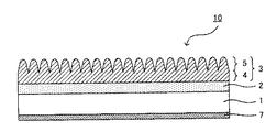
本発明の反射防止フィルムについて、図面を参照しながら説明する。図1は、本発明の反射防止フィルムの一例を示す概略断面図である。なお、図1(a)は反射防止フィルム全体を示しており、図1(b)は図1(a)に示す反射防止フィルムにおける反射防止層を拡大して示している。図1(a)に例示する反射防止フィルム10は、ポリエチレンテレフタレート(PET)樹脂からなる光透過性基板1と、光透過性基板1上に形成された易接着層2と、易接着層2上に形成され、表面に可視光領域の表面に可視光領域の波長以下の周期で形成された凹凸形状を有する反射防止層3とを有している。また、易接着層2は、光透過性基板1の屈折率と、反射防止層3の屈折率との平均となる屈折率を有し、反射防止層3は、易接着層2上に形成された基底部4と、基底部4上に形成され、上記凹凸形状からなる微細凹凸5とを有している。さらに、図1(b)に例示するように、微細凹凸5における凸部は、光透過性基板に対してテーパー状に立ち上がる錐台形状の本体部5aと、本体部5aの頂面を覆うように形成された曲面構造を有する先端部5bとから構成されている。
The antireflection film of the present invention will be described with reference to the drawings. FIG. 1 is a schematic sectional view showing an example of the antireflection film of the present invention. 1A shows the entire antireflection film, and FIG. 1B shows an enlarged antireflection layer in the antireflection film shown in FIG. 1A. An
本発明によれば、光透過性基板および反射防止層の間に易接着層を形成することで、反射防止層と光透過性基板との密着性を向上させることができ、かつ、易接着層が所定の屈折率を有することにより、干渉縞の発生を防止し、反射ムラを抑制することができる。加えて、PET樹脂からなる光透過性基板を用いることで、安価な反射防止フィルムとすることができる。また、本発明によれば、反射防止層の微細凹凸における凸部が、光透過性基板に対してテーパー状に立ち上がる錐台形状の本体部の頂面を覆うように形成された曲面構造を有する先端部を備えているため、良好な反射防止機能を有するとともに、反射防止層における微細凹凸パターンの凸部先端の割れ等に対する機械強度、スティッキング耐性および型抜き性に優れた反射防止フィルムとすることができる。さらに、上記微細凹凸における凸部が、上記錐台形状の本体部を有しているため、反射防止フィルムを製造する際に用いる金型から抜けやすい反射防止フィルムとすることができる。 According to the present invention, the adhesion between the antireflection layer and the light transmissive substrate can be improved by forming the easy adhesion layer between the light transmissive substrate and the antireflection layer, and the easy adhesion layer. By having a predetermined refractive index, generation of interference fringes can be prevented and reflection unevenness can be suppressed. In addition, by using a light-transmitting substrate made of PET resin, an inexpensive antireflection film can be obtained. Further, according to the present invention, the convex portion in the fine unevenness of the antireflection layer has a curved surface structure formed so as to cover the top surface of the frustum-shaped main body portion that rises in a tapered shape with respect to the light-transmitting substrate. Since it has a tip, it has a good anti-reflection function, and it should be an anti-reflection film with excellent mechanical strength, sticking resistance and die-cutting properties against cracks at the tip of the convex part of the fine uneven pattern in the anti-reflection layer. Can do. Furthermore, since the convex part in the said fine unevenness | corrugation has the said frustum-shaped main-body part, it can be set as the antireflection film which is easy to come off from the metal mold | die used when manufacturing an antireflection film.
本発明の反射防止フィルムは、少なくとも光透過性基板と、易接着層と、反射防止層とを有するものであり、必要に応じて他の任意の構成を有していてもよいものである。
以下、本発明の反射防止フィルムにおける各構成について説明する。
The antireflection film of the present invention has at least a light-transmitting substrate, an easy-adhesion layer, and an antireflection layer, and may have any other configuration as necessary.
Hereinafter, each structure in the antireflection film of the present invention will be described.
1.易接着層
まず、本発明における易接着層について説明する。本発明における易接着層は、ポリエチレンテレフタレート(PET)樹脂からなる光透過性基板上に形成されるものであり、光透過性基板の屈折率と、反射防止層の屈折率との平均となる屈折率を有するものである。本発明においては、光透過性基板および反射防止層の間に、所定の屈折率を有する易接着層を形成することにより、光透過性基板と反射防止層との密着性を向上させることができ、かつ、干渉縞の発生を防止することができる。
1. Easy-Adhesion Layer First, the easy-adhesion layer in the present invention will be described. The easy adhesion layer in the present invention is formed on a light-transmitting substrate made of polyethylene terephthalate (PET) resin, and is a refractive index that is an average of the refractive index of the light-transmitting substrate and the refractive index of the antireflection layer. Has a rate. In the present invention, the adhesion between the light transmissive substrate and the antireflection layer can be improved by forming an easy-adhesion layer having a predetermined refractive index between the light transmissive substrate and the antireflection layer. And generation | occurrence | production of an interference fringe can be prevented.
本発明における易接着層は、通常、樹脂からなるものである。易接着層に用いられる樹脂としては、紫外線硬化性樹脂、熱硬化性樹脂(2液硬化性樹脂を含む)、熱可塑性樹脂を挙げることができる。
紫外線硬化性樹脂としては、特に限定されるものではないが、例えば、少なくとも3つ以上のエチレン性不飽和二重結合を有する化合物が挙げられる。具体的には、ペンタエリスリトールトリ(メタ)アクリレート、ペンタエリスリトールテトラ(メタ)アクリレート、トリメチロールプロパントリ(メタ)アクリレート、EO変性トリメチロールプロパントリ(メタ)アクリレート、PO変性トリメチロールプロパントリ(メタ)アクリレート、トリス(アクリロキシエチル)イソシアヌレート、カプロラクトン変性トリス(アクリロキシエチル)イソシアヌレート、トリメチロールエタントリ(メタ)アクリレート、ジペンタエリスリトールテトラ(メタ)アクリレート、ジペンタエリスリトールペンタ(メタ)アクリレート、ジペンタエリスリトールヘキサ(メタ)アクリレート、アルキル変性ジペンタエリスリトールトリ(メタ)アクリレート、アルキル変性ジペンタエリスリトールテトラ(メタ)アクリレート、アルキル変性ジペンタエリスリトールペンタ(メタ)アクリレート、カプロラクトン変性ジペンタエリスリトールヘキサ(メタ)アクリレート、1,2,3−シクロヘキサンテトラ(メタ)アクリレート、ポリウレタンポリアクリレート、ポリエステルポリアクリレート等の多価アルコールと(メタ)アクリル酸とのエステル化合物;ポリウレタンポリ(メタ)アクリレート、ポリエステルポリ(メタ)アクリレート、ポリエーテルポリ(メタ)アクリレート、ポリアクリルポリ(メタ)アクリレート、ポリアルキッドポリ(メタ)アクリレート、ポリエポキシポリ(メタ)アクリレート、ポリスピロアセタールポリ(メタ)アクリレート、ポリブタジエンポリ(メタ)アクリレート、ポリチオールポリエンポリ(メタ)アクリレート、ポリシリコンポリ(メタ)アクリレート等の多官能化合物の(メタ)アクリレート化合物等が挙げられる。
これら少なくとも3つ以上のエチレン性不飽和二重結合を有する化合物のうち、塗膜強度、密着性の観点より、少なくとも6つの官能基を有するポリウレタンポリ(メタ)アクリレート、ポリエポキシポリ(メタ)アクリレート等のポリ(メタ)アクリレート類、分子内に4個以上のアクリロイル基を有する多官能のアクリレート類を好適に使用することができる。
ポリウレタンポリ(メタ)アクリレートは、例えば、ジイソシアネートと水酸基を有する(メタ)アクリレート類と反応させて得られるもの、ポリオールとポリイソシアネートとをイソシアネート基過剰の条件下に反応させてなるイソシアネート基含有ウレタンプレポリマーを、水酸基を有する(メタ)アクリレート類と反応させて得られるものがある。あるいは、ポリオールとポリイソシアネートとを水酸基過剰の条件下に反応させてなる水酸基含有ウレタンプレポリマーを、イソシアネート基を有する(メタ)アクリレート類と反応させて得ることもできる。
ポリオールとしては、エチレングリコール、プロピレングリコール、ジエチレングリコール、ジプロピレングリコール、ブチレングリコール、1,6−ヘキサンジオール、3−メチル−1,5−ペンタングリコール、ネオペンチルグリコール、ヘキサントリオール、トリメリロールプロパン、ポリテトラメチレングリコール、アジピン酸とエチレングリコールとの縮重合物等が挙げられる。
ポリイソシアネートとしては、トリレンジイソシアネート、イソホロンジイソシアネート、ヘキサメチレンジイソシアネート等が挙げられる。
水酸基を有する(メタ)アクリレート類としては、2−ヒドロキシエチルアクリレート、2−ヒドロキシプロピルアクリテート、4−ヒドロキシブチルアクリレート、ペンタエリスリトールトリアクリレート、ジペンタエリスリトールペンタアクリレート、ジトリメチロールプロパンテトラアクリレート等が挙げられる。
イソシアネート基を有する(メタ)アクリレート類としては、2−メタクリロイルオキシエチルイソシアネート、メタクリロイルイソシアネート等が挙げられる。
ポリエポキシポリ(メタ)アクリレートは、エポキシ樹脂のエポキシ基を(メタ)アクリル酸でエステル化し官能基を(メタ)アクリロイル基としたものであり、ビスフェノールA型エポキシ樹脂への(メタ)アクリル酸付加物、ノボラック型エポキシ樹脂への(メタ)アクリル酸付加物等がある。
分子内に4個以上のアクリロイル基を有する多官能としては、具体的には上記多価アルコールとアクリル酸のエステル化合物が挙げられ、単独または2種以上の混合物が好ましい。
さらに、WO2007/040159に記載されている(メタ)アクリル系重合性組成物を用いることができる。
The easy-adhesion layer in the present invention is usually made of a resin. Examples of the resin used for the easy adhesion layer include an ultraviolet curable resin, a thermosetting resin (including a two-component curable resin), and a thermoplastic resin.
Although it does not specifically limit as an ultraviolet curable resin, For example, the compound which has an at least 3 or more ethylenically unsaturated double bond is mentioned. Specifically, pentaerythritol tri (meth) acrylate, pentaerythritol tetra (meth) acrylate, trimethylolpropane tri (meth) acrylate, EO-modified trimethylolpropane tri (meth) acrylate, PO-modified trimethylolpropane tri (meth) Acrylate, tris (acryloxyethyl) isocyanurate, caprolactone-modified tris (acryloxyethyl) isocyanurate, trimethylolethane tri (meth) acrylate, dipentaerythritol tetra (meth) acrylate, dipentaerythritol penta (meth) acrylate, di Pentaerythritol hexa (meth) acrylate, alkyl-modified dipentaerythritol tri (meth) acrylate, alkyl-modified dipentaerythritol Such as tra (meth) acrylate, alkyl-modified dipentaerythritol penta (meth) acrylate, caprolactone-modified dipentaerythritol hexa (meth) acrylate, 1,2,3-cyclohexanetetra (meth) acrylate, polyurethane polyacrylate, polyester polyacrylate, etc. Ester compound of polyhydric alcohol and (meth) acrylic acid; polyurethane poly (meth) acrylate, polyester poly (meth) acrylate, polyether poly (meth) acrylate, polyacryl poly (meth) acrylate, polyalkyd poly (meth) Acrylate, polyepoxy poly (meth) acrylate, polyspiroacetal poly (meth) acrylate, polybutadiene poly (meth) acrylate, polythiol polyempo (Meth) acrylates, (meth) acrylate compound of the polysilicon poly (meth) polyfunctional compounds such acrylate.
Among these compounds having at least three or more ethylenically unsaturated double bonds, polyurethane poly (meth) acrylate and polyepoxy poly (meth) acrylate having at least six functional groups from the viewpoint of coating film strength and adhesion. Poly (meth) acrylates such as polyfunctional acrylates having 4 or more acryloyl groups in the molecule can be suitably used.
The polyurethane poly (meth) acrylate is obtained by reacting, for example, a diisocyanate and a (meth) acrylate having a hydroxyl group, or an isocyanate group-containing urethane prepolymer obtained by reacting a polyol and a polyisocyanate under an excess of isocyanate groups. Some are obtained by reacting polymers with (meth) acrylates having a hydroxyl group. Alternatively, a hydroxyl group-containing urethane prepolymer obtained by reacting a polyol and a polyisocyanate under hydroxyl-excess conditions can be obtained by reacting with a (meth) acrylate having an isocyanate group.
Examples of polyols include ethylene glycol, propylene glycol, diethylene glycol, dipropylene glycol, butylene glycol, 1,6-hexanediol, 3-methyl-1,5-pentane glycol, neopentyl glycol, hexanetriol, trimellilol propane, polytetra Examples include methylene glycol and a condensation polymer of adipic acid and ethylene glycol.
Examples of the polyisocyanate include tolylene diisocyanate, isophorone diisocyanate, and hexamethylene diisocyanate.
Examples of (meth) acrylates having a hydroxyl group include 2-hydroxyethyl acrylate, 2-hydroxypropyl acrylate, 4-hydroxybutyl acrylate, pentaerythritol triacrylate, dipentaerythritol pentaacrylate, and ditrimethylolpropane tetraacrylate. .
Examples of (meth) acrylates having an isocyanate group include 2-methacryloyloxyethyl isocyanate and methacryloyl isocyanate.
Polyepoxy poly (meth) acrylate is an epoxy resin whose ester group is esterified with (meth) acrylic acid and whose functional group is (meth) acryloyl group, and (meth) acrylic acid addition to bisphenol A type epoxy resin Products, (meth) acrylic acid addition products to novolac type epoxy resins, and the like.
Specific examples of the polyfunctional group having four or more acryloyl groups in the molecule include the above-mentioned polyhydric alcohol and acrylic acid ester compounds, and a single compound or a mixture of two or more compounds is preferred.
Furthermore, a (meth) acrylic polymerizable composition described in WO2007 / 040159 can be used.
また、熱硬化性樹脂あるいは熱可塑性樹脂としては、例えば、アクリル樹脂、ポリエステル樹脂、エポキシ樹脂、ポリオレフィン樹脂、ポリエチレンイミン樹脂、ポリエーテル樹脂、ポリエーテルウレタン樹脂、ポリエステルウレタン樹脂、スチロール樹脂、ポリアミド樹脂、ポリイミド樹脂、ポリアミドイミド樹脂、ポリウレタン樹脂、ポリ酢酸ビニル樹脂、ポリビニルアルコール樹脂、ポリビニルブチラール樹脂、ポリカーボネート樹脂、メラミン樹脂、尿素樹脂、アルキッド樹脂、フェノール樹脂、セルロース樹脂、ジアリルフタレート樹脂、シリコーン樹脂、ポリアリレート樹脂、ポリアセタール樹脂、スチレン−イソプレンゴム、オレフィン・マレイミド共重合体、フルオレイン系エポキシ、フルオレイン系アクリレート、フルオレイン系ポリエステル、フッ素樹脂等を挙げることができる。 Examples of the thermosetting resin or thermoplastic resin include acrylic resin, polyester resin, epoxy resin, polyolefin resin, polyethyleneimine resin, polyether resin, polyether urethane resin, polyester urethane resin, styrene resin, polyamide resin, Polyimide resin, polyamideimide resin, polyurethane resin, polyvinyl acetate resin, polyvinyl alcohol resin, polyvinyl butyral resin, polycarbonate resin, melamine resin, urea resin, alkyd resin, phenol resin, cellulose resin, diallyl phthalate resin, silicone resin, polyarylate Resin, Polyacetal resin, Styrene-isoprene rubber, Olefin / maleimide copolymer, Fluorine epoxy, Fluorine acrylate, Fluoro Mention may be made in polyester, a fluorine resin, or the like.
本発明における易接着層の透明度としては、可視光の全波長範囲に対する光の透過率が80%以上であることが好ましく、85%以上であることがより好ましく、90%以上であることがさらに好ましい。
ここで、上記光の透過率は、例えば、株式会社日立ハイテクノロジーズ製分光光度計、U−4100により測定することができる。
As the transparency of the easy-adhesion layer in the present invention, the light transmittance with respect to the entire wavelength range of visible light is preferably 80% or more, more preferably 85% or more, and further preferably 90% or more. preferable.
Here, the light transmittance can be measured by, for example, a spectrophotometer U-4100 manufactured by Hitachi High-Technologies Corporation.
本発明における易接着層の屈折率は、後述する光透過性基板の屈折率および反射防止層の屈折率の平均となる。ここで、「光透過性基板の屈折率および反射防止層の屈折率の平均となる」とは、「光透過性基板の屈折率および反射防止層の屈折率の算術平均値の±2.5%の範囲内となる」ことをいう。
本発明においては、反射防止層の屈折率を光透過性基板の屈折率に近いものとすることにより、易接着層の屈折率が、光透過性基板の屈折率および反射防止層の屈折率となるべく近い値となることが好ましい。これにより、本発明の反射防止フィルムにおいて、反射防止層と易接着層と光透過性基板との各界面に、屈折率の不連続界面が形成され、当該不連続界面において光が反射されることにより、上記反射防止フィルムの反射防止機能が損なわれることを防止することができるからである。中でも、上記易接着層の屈折率は、反射防止層の屈折率および光透過性基板の屈折率との差が0〜0.5の範囲内であることが好ましく、0〜0.2の範囲内であることがより好ましく、0〜0.1の範囲内であることがさらに好ましい。
なお、本発明における易接着層の屈折率の値は、光透過性基板の屈折率および反射防止層の屈折率によって決定されるものであるから、特に好ましい値はないが、通常、1.20〜2.40の範囲内とされる。
The refractive index of the easy-adhesion layer in the present invention is the average of the refractive index of the light-transmitting substrate and the refractive index of the antireflection layer described later. Here, “becomes the average of the refractive index of the light transmissive substrate and the refractive index of the antireflection layer” means “± 2.5 of the arithmetic average value of the refractive index of the light transmissive substrate and the refractive index of the antireflection layer”. % ”.
In the present invention, by making the refractive index of the anti-reflection layer close to the refractive index of the light-transmitting substrate, the refractive index of the easy-adhesion layer is the same as the refractive index of the light-transmitting substrate and the refractive index of the anti-reflection layer. It is preferable that the value be as close as possible. Thereby, in the antireflection film of the present invention, a discontinuous interface of refractive index is formed at each interface of the antireflection layer, the easy-adhesion layer, and the light-transmitting substrate, and light is reflected at the discontinuous interface. This is because the antireflection function of the antireflection film can be prevented from being impaired. Among these, the refractive index of the easy-adhesion layer is preferably such that the difference between the refractive index of the antireflection layer and the refractive index of the light-transmitting substrate is in the range of 0 to 0.5, and is in the range of 0 to 0.2. It is more preferable that it is in the range of 0 to 0.1.
In the present invention, the refractive index value of the easy-adhesion layer is determined by the refractive index of the light-transmitting substrate and the refractive index of the antireflection layer. It is set within the range of ~ 2.40.
また、本発明における易接着層は、単層であってもよく、多層であってもよい。易接着層が多層である場合は、易接着層を構成する各層の屈折率を平均した平均屈折率が、光透過性基板の屈折率と、反射防止層の屈折率との平均となる。易接着層が多層の場合、光透過性基板の屈折率>易接着層の屈折率>反射防止層の屈折率となることが望ましい。 In addition, the easy adhesion layer in the present invention may be a single layer or a multilayer. When the easy adhesion layer is a multilayer, the average refractive index obtained by averaging the refractive indexes of the layers constituting the easy adhesion layer is the average of the refractive index of the light-transmitting substrate and the refractive index of the antireflection layer. When the easy adhesion layer is a multilayer, it is desirable that the refractive index of the light-transmitting substrate> the refractive index of the easy adhesion layer> the refractive index of the antireflection layer.
本発明の易接着層の厚みとしては、反射防止層と光透過性基板との密着性を向上させることができ、かつ、干渉縞の発生を防止することができる範囲内であれば特に限定されるものではないが、0.01μm〜10.0μmの範囲内であることが好ましく、0.05μm〜5.0μmの範囲内であることがより好ましく、0.10μm〜2.0μmの範囲内であることがさらに好ましい。易接着層の厚みが上記範囲よりも厚いと、本発明の反射防止フィルムにカールが生じてしまうおそれがあるからであり、易接着層の厚みが上記範囲よりも薄いと、易接着層に所望の硬度を付与することが困難となるおそれがあるからである。 The thickness of the easy-adhesion layer of the present invention is not particularly limited as long as the adhesion between the antireflection layer and the light-transmitting substrate can be improved and interference fringes can be prevented. Although not intended, it is preferably within the range of 0.01 μm to 10.0 μm, more preferably within the range of 0.05 μm to 5.0 μm, and within the range of 0.10 μm to 2.0 μm. More preferably it is. If the thickness of the easy-adhesion layer is larger than the above range, curling may occur in the antireflection film of the present invention. If the thickness of the easy-adhesion layer is smaller than the above range, it is desirable for the easy-adhesion layer. This is because it may be difficult to impart the hardness of.
本発明における易接着層は、上述した樹脂の他に、必要に応じて任意の添加剤を含有していてもよい。このような添加剤としては、本発明の易接着層に所望の機能を付与できるものであれば特に限定されるものではないが、例えば、帯電防止剤(導電剤)、屈折率調整剤、レベリング剤、防汚染剤、粘着剤、紫外線・赤外線吸収剤、高硬度化剤、硬度調整剤、流動性調整剤、酸化防止剤、フッ素系樹脂、流動パラフィン、パラフィンワックス、合成ポリエチレンワックスなどの炭化水素系、脂肪酸アマイド系、ステアリン酸金属塩、ステアリン酸カルシウム・ステアリン酸マグネシウム、ステアリン酸鉛・ステアリン酸亜鉛などの金属石鹸系、脂肪酸エステル系、シリコーンオイル系、アクリル系高分子系などの離型剤や内部または外部滑剤、炭酸ストロンチウムなどの偏屈折調整剤、親水性剤、親油性剤、着色剤等を挙げることができる。具体的には、例えば、特開2009−230045号公報に記載されている以下の物質が挙げられる。 The easy-adhesion layer in the present invention may contain any additive as necessary in addition to the above-described resin. Such an additive is not particularly limited as long as a desired function can be imparted to the easy-adhesion layer of the present invention, and examples thereof include an antistatic agent (conductive agent), a refractive index adjusting agent, and a leveling. Agents, antifouling agents, adhesives, ultraviolet and infrared absorbers, hardeners, hardness modifiers, fluidity modifiers, antioxidants, fluororesins, liquid paraffin, paraffin wax, synthetic polyethylene wax and other hydrocarbons Release agents such as metal soaps, fatty acid amides, metal stearates, metal soaps such as calcium stearate / magnesium stearate, lead stearate / zinc stearate, fatty acid esters, silicone oils, acrylic polymers Examples thereof include an internal or external lubricant, a polarization refraction adjusting agent such as strontium carbonate, a hydrophilic agent, a lipophilic agent, and a coloring agent. Specifically, for example, the following substances described in JP 2009-230045 A can be mentioned.
<帯電防止剤(導電剤)>
帯電防止剤(導電剤)を添加することにより、易接着層の表面における塵埃付着を有効に防止することができる。帯電防止剤(導電剤)の具体例としては、第4級アンモニウム塩、ピリジニウム塩、第1〜第3アミノ基等のカチオン性基を有する各種のカチオン性化合物、スルホン酸塩基、硫酸エステル塩基、リン酸エステル塩基、ホスホン酸塩基等のアニオン性基を有するアニオン性化合物、アミノ酸系、アミノ硫酸エステル系等の両性化合物、アミノアルコール系、グリセリン系、ポリエチレングリコール系等のノニオン性化合物、スズおよびチタンのアルコキシドのような有機金属化合物およびそれらのアセチルアセトナート塩のような金属キレート化合物等が挙げられ、さらに上記に列記した化合物を高分子量化した化合物が挙げられる。また、第3級アミノ基、第4級アンモニウム基、または金属キレート部を有し、かつ、電離放射線により重合可能なモノマーまたはオリゴマー、あるいは官能基を有するカップリング剤のような有機金属化合物等の重合性化合物もまた帯電防止剤として使用できる。
<Antistatic agent (conductive agent)>
By adding an antistatic agent (conductive agent), dust adhesion on the surface of the easy-adhesion layer can be effectively prevented. Specific examples of the antistatic agent (conductive agent) include quaternary ammonium salts, pyridinium salts, various cationic compounds having a cationic group such as first to third amino groups, sulfonate groups, sulfate ester bases, Anionic compounds having an anionic group such as phosphate ester base and phosphonate base, amphoteric compounds such as amino acid series and amino sulfate ester series, nonionic compounds such as amino alcohol series, glycerin series and polyethylene glycol series, tin and titanium And metal chelate compounds such as acetylacetonate salts thereof, and compounds obtained by increasing the molecular weight of the compounds listed above. In addition, a monomer or oligomer having a tertiary amino group, a quaternary ammonium group, or a metal chelate portion and polymerizable by ionizing radiation, or an organometallic compound such as a coupling agent having a functional group, etc. Polymerizable compounds can also be used as antistatic agents.
また、帯電防止剤として、導電性ポリマーが挙げられ、その具体例としては、脂肪族共役系のポリアセチレン、ポリアセン、オリアズレン等;芳香族共役系のポリ(パラフェニレン)等;複素環式共役系のポリピロール、ポリチオフェン、ポリイソシアナフテン等;含ヘテロ原子共役系のポリアニリン、ポリチエニレンビニレン等;混合型共役系のポリ(フェニレンビニレン)等が挙げられ、これら以外に、分子中に複数の共役鎖を持つ共役系である複鎖型共役系、前述の共役高分子鎖を飽和高分子にグラフトまたはブロック共重した高分子である導電性複合体、これら導電性ポリマー誘導体等が挙げられる。取り分け、ポリピロール、ポリチオフェン、ポリアニリン等の有機系帯電防止剤を使用することがより好ましい。上記有機系帯電防止剤を使用することによって、優れた帯電防止性能を発揮すると同時に、易接着層の全光線透過率を高めるとともにヘイズ値を下げることも可能になる。また、導電性向上や、帯電防止性能向上を目的として、有機スルホン酸や塩化鉄等の陰イオンを、ドーパント(電子供与剤)として添加することもできる。ドーパント添加効果も踏まえ、特にポリチオフェンは透明性、帯電防止性が高く、好ましい。上記ポリチオフェンとしては、オリゴチオフェンも好適に使用することができる。上記誘導体としては特に限定されず、例えば、ポリフェニルアセチレン、ポリジアセチレンのアルキル基置換体等を挙げることができる。また、導電性カーボンナノチューブ、ボロンおよびその化合物等が挙げられる。また、金属、およびこれらの金属酸化物の粒子径1μm以下の微粉末を添加することもできる。例えば、チタン、アルミニウム、セリウム、イットリウム、ジルコニウム、ニオブ、アンチモンからなる金属、または金属酸化物、あるいはこれらを表面に被覆またはドープした化合物が用いられる。 Examples of the antistatic agent include conductive polymers, and specific examples thereof include aliphatic conjugated polyacetylene, polyacene, oliazulene, etc .; aromatic conjugated poly (paraphenylene), etc .; heterocyclic conjugated type Examples include polypyrrole, polythiophene, polyisocyannaphthene, etc .; heteroatom-containing polyaniline, polythienylene vinylene, etc .; mixed conjugated poly (phenylene vinylene), etc. In addition to these, a plurality of conjugated chains are included in the molecule. Examples thereof include a double-chain conjugated system that is a conjugated system, a conductive composite that is a polymer obtained by grafting or block-copolymerizing the conjugated polymer chain described above to a saturated polymer, and these conductive polymer derivatives. In particular, it is more preferable to use an organic antistatic agent such as polypyrrole, polythiophene or polyaniline. By using the above-mentioned organic antistatic agent, it is possible to exhibit excellent antistatic performance and at the same time increase the total light transmittance of the easy-adhesive layer and reduce the haze value. An anion such as an organic sulfonic acid or iron chloride can be added as a dopant (electron donor) for the purpose of improving conductivity and improving antistatic performance. In view of the effect of dopant addition, polythiophene is particularly preferable because of its high transparency and antistatic properties. As the polythiophene, oligothiophene can also be preferably used. The derivative is not particularly limited, and examples thereof include polyphenylacetylene, polydiacetylene alkyl group-substituted products, and the like. In addition, conductive carbon nanotubes, boron, and compounds thereof can be used. Metals and fine powders of these metal oxides having a particle diameter of 1 μm or less can also be added. For example, a metal made of titanium, aluminum, cerium, yttrium, zirconium, niobium, antimony, or a metal oxide, or a compound in which these are coated or doped on the surface is used.
本発明の好ましい態様によれば、帯電防止剤は、易接着層を形成する際に用いられる易接着層形成用樹脂組成物全量に対して、0.01重量%以上50重量%以下であり、好ましくは下限値が0.1重量%以上であり上限値が30重量%以下程度である。上記数値範囲に調整することにより、易接着層としての透明性を保ち、また易接着層の機能に影響を与えることなく、帯電防止性能を付与することができる点で好ましい。 According to a preferred aspect of the present invention, the antistatic agent is 0.01% by weight or more and 50% by weight or less based on the total amount of the resin composition for forming an easy adhesion layer used when forming the easy adhesion layer. Preferably, the lower limit is 0.1% by weight or more and the upper limit is about 30% by weight or less. By adjusting to the above numerical range, it is preferable in that the transparency as the easy-adhesion layer is maintained and the antistatic performance can be imparted without affecting the function of the easy-adhesion layer.
<屈折率調整剤>
屈折率調整剤を添加することにより、易接着層の光学特性を調整することが可能となる。屈折率調整剤には、低屈折率剤、中屈折率剤、高屈折率剤等が挙げられる。
<Refractive index modifier>
By adding a refractive index adjusting agent, it is possible to adjust the optical characteristics of the easy adhesion layer. Examples of the refractive index adjusting agent include a low refractive index agent, a medium refractive index agent, and a high refractive index agent.
1)低屈折率剤
低屈折率剤を添加した易接着層の屈折率は、1.5未満であり、好ましくは1.45以下で構成されてなるものが好ましい。低屈折率剤の好ましいものとしては、シリカ、フッ化マグネシウムなどの低屈折率無機超微粒子(多孔質、中空など全ての種類の微粒子)、および低屈折率樹脂であるフッ素系樹脂が挙げられる。フッ素系樹脂としては、少なくとも分子中にフッ素原子を含む重合性化合物またはその重合体を用いることができる。重合性化合物は、特に限定されないが、例えば、電離放射線で硬化する官能基、熱硬化する極性基等の硬化反応性の基を有するものが好ましい。また、これらの反応性の基を同時に併せ持つ化合物でもよい。この重合性化合物に対し、重合体とは、上記のような反応性基などを一切もたないものである。
1) Low refractive index agent The refractive index of the easy-adhesion layer to which the low refractive index agent is added is less than 1.5, preferably 1.45 or less. Preferable examples of the low refractive index agent include low refractive index inorganic ultrafine particles such as silica and magnesium fluoride (all kinds of fine particles such as porous and hollow), and fluorine-based resins which are low refractive index resins. As the fluororesin, a polymerizable compound containing at least a fluorine atom in the molecule or a polymer thereof can be used. The polymerizable compound is not particularly limited, but for example, those having a curing reactive group such as a functional group that is cured by ionizing radiation and a polar group that is thermally cured are preferable. Moreover, the compound which has these reactive groups simultaneously may be sufficient. In contrast to this polymerizable compound, a polymer has no reactive groups as described above.
電離放射線硬化性基を有する重合性化合物としては、エチレン性不飽和結合を有するフッ素含有モノマーを広く用いることができる。より具体的には、フルオロオレフィン類(例えばフルオロエチレン、ビニリデンフルオライド、テトラフルオロエチレン、ヘキサフルオロプロピレン、パーフルオロブタジエン、パーフルオロ−2,2−ジメチル−1,3−ジオキソールなど)を例示することができる。(メタ)アクリロイルオキシ基を有するものとして、2,2,2−トリフルオロエチル(メタ)アクリレート、2,2,3,3,3−ペンタフルオロプロピル(メタ)アクリレート、2−(パーフルオロブチル)エチル(メタ)アクリレート、2−(パーフルオロヘキシル)エチル(メタ)アクリレート、2−(パーフルオロオクチル)エチル(メタ)アクリレート、2−(パーフルオロデシル)エチル(メタ)アクリレート、α−トリフルオロメタクリル酸メチル、α−トリフルオロメタクリル酸エチルのような、分子中にフッ素原子を有する(メタ)アクリレート化合物;分子中に、フッ素原子を少なくとも3個持つ炭素数1〜14のフルオロアルキル基、フルオロシクロアルキル基またはフルオロアルキレン基と、少なくとも2個の(メタ)アクリロイルオキシ基とを有する含フッ素多官能(メタ)アクリル酸エステル化合物などもある。 As the polymerizable compound having an ionizing radiation curable group, fluorine-containing monomers having an ethylenically unsaturated bond can be widely used. More specifically, to illustrate fluoroolefins (eg, fluoroethylene, vinylidene fluoride, tetrafluoroethylene, hexafluoropropylene, perfluorobutadiene, perfluoro-2,2-dimethyl-1,3-dioxole, etc.) Can do. As having a (meth) acryloyloxy group, 2,2,2-trifluoroethyl (meth) acrylate, 2,2,3,3,3-pentafluoropropyl (meth) acrylate, 2- (perfluorobutyl) Ethyl (meth) acrylate, 2- (perfluorohexyl) ethyl (meth) acrylate, 2- (perfluorooctyl) ethyl (meth) acrylate, 2- (perfluorodecyl) ethyl (meth) acrylate, α-trifluoromethacryl (Meth) acrylate compounds having fluorine atoms in the molecule, such as methyl acrylate and ethyl α-trifluoromethacrylate; C 1-14 fluoroalkyl groups having at least 3 fluorine atoms in the molecule, fluorocyclo An alkyl group or a fluoroalkylene group and at least two (medium There are also fluorine-containing polyfunctional (meth) acrylic acid ester compounds having an acryloyloxy group.
熱硬化性極性基として好ましいのは、例えば水酸基、カルボキシル基、アミノ基、エポキシ基等の水素結合形成基である。これらは、塗膜との密着性だけでなく、シリカなどの無機超微粒子との親和性にも優れている。熱硬化性極性基を持つ重合成化合物としては、例えば、4−フルオロエチレン−パーフルオロアルキルビニルエーテル共重合体;フルオロエチレン−炭化水素系ビニルエーテル共重合体;エポキシ、ポリウレタン、セルロース、フェノール、ポリイミド等の各樹脂のフッ素変性品などを挙げることができる。 Preferable examples of the thermosetting polar group include hydrogen bond forming groups such as a hydroxyl group, a carboxyl group, an amino group, and an epoxy group. These are excellent not only in adhesion to the coating film but also in affinity with inorganic ultrafine particles such as silica. Examples of the polysynthetic compound having a thermosetting polar group include 4-fluoroethylene-perfluoroalkyl vinyl ether copolymer; fluoroethylene-hydrocarbon vinyl ether copolymer; epoxy, polyurethane, cellulose, phenol, polyimide, etc. Fluorine modified products of each resin can be mentioned.
電離放射線硬化性基と熱硬化性極性基とを併せ持つ重合性化合物としては、アクリルまたはメタクリル酸の部分および完全フッ素化アルキル、アルケニル、アリールエステル類、完全または部分フッ素化ビニルエーテル類、完全または部分フッ素化ビニルエステル類、完全または部分フッ素化ビニルケトン類等を例示することができる。 Polymerizable compounds having both ionizing radiation curable groups and thermosetting polar groups include acrylic or methacrylic acid moieties and fully fluorinated alkyl, alkenyl, aryl esters, fully or partially fluorinated vinyl ethers, fully or partially fluorine. Illustrative examples include fluorinated vinyl esters, fully or partially fluorinated vinyl ketones, and the like.
また、含フッ素重合体の具体例としては、上記電離放射線硬化性基を有する重合性化合物の含フッ素(メタ)アクリレート化合物を少なくとも1種類含むモノマーまたはモノマー混合物の重合体;上記含フッ素(メタ)アクリレート化合物の少なくとも1種類と、メチル(メタ)アクリレート、エチル(メタ)アクリレート、プロピル(メタ)アクリレート、ブチル(メタ)アクリレート、2−エチルヘキシル(メタ)アクリレートの如き分子中にフッ素原子を含まない(メタ)アクリレート化合物との共重合体;フルオロエチレン、フッ化ビニリデン、トリフルオロエチレン、クロロトリフルオロエチレン、3,3,3−トリフルオロプロピレン、1,1,2−トリクロロ−3,3,3−トリフルオロプロピレン、ヘキサフルオロプロピレンのような含フッ素モノマーの単独重合体または共重合体等が挙げられる。 Specific examples of the fluorine-containing polymer include a polymer of a monomer or a monomer mixture containing at least one fluorine-containing (meth) acrylate compound of the polymerizable compound having the ionizing radiation curable group; the fluorine-containing (meth) At least one kind of acrylate compound and no fluorine atom in the molecule such as methyl (meth) acrylate, ethyl (meth) acrylate, propyl (meth) acrylate, butyl (meth) acrylate, 2-ethylhexyl (meth) acrylate ( Copolymer with (meth) acrylate compound; fluoroethylene, vinylidene fluoride, trifluoroethylene, chlorotrifluoroethylene, 3,3,3-trifluoropropylene, 1,1,2-trichloro-3,3,3- Trifluoropropylene, hexafluoropropylene Homopolymers or copolymers of fluorine-containing monomer are mentioned, such as.
これらの共重合体にシリコーン成分を含有させたシリコーン含有フッ化ビニリデン共重合体も使うことができる。この場合のシリコーン成分としては、(ポリ)ジメチルシロキサン、(ポリ)ジエチルシロキサン、(ポリ)ジフェニルシロキサン、(ポリ)メチルフェニルシロキサン、アルキル変性(ポリ)ジメチルシロキサン、アゾ基含有(ポリ)ジメチルシロキサン、ジメチルシリコーン、フェニルメチルシリコーン、アルキル・アラルキル変性シリコーン、フルオロシリコーン、ポリエーテル変性シリコーン、脂肪酸エステル変性シリコーン、メチル水素シリコーン、シラノール基含有シリコーン、アルコキシ基含有シリコーン、フェノール基含有シリコーン、メタクリル変性シリコーン、アクリル変性シリコーン、アミノ変性シリコーン、カルボン酸変性シリコーン、カルビノール変性シリコーン、エポキシ変性シリコーン、メルカプト変性シリコーン、フッ素変性シリコーン、ポリエーテル変性シリコーン等が例示される。中でもジメチルシロキサン構造を有するものが好ましい。 Silicone-containing vinylidene fluoride copolymers obtained by adding a silicone component to these copolymers can also be used. The silicone components in this case include (poly) dimethylsiloxane, (poly) diethylsiloxane, (poly) diphenylsiloxane, (poly) methylphenylsiloxane, alkyl-modified (poly) dimethylsiloxane, azo group-containing (poly) dimethylsiloxane, Dimethyl silicone, phenylmethyl silicone, alkyl aralkyl modified silicone, fluorosilicone, polyether modified silicone, fatty acid ester modified silicone, methyl hydrogen silicone, silanol group containing silicone, alkoxy group containing silicone, phenol group containing silicone, methacryl modified silicone, acrylic Modified silicone, amino modified silicone, carboxylic acid modified silicone, carbinol modified silicone, epoxy modified silicone, mercapto modified silicone Over emissions, fluorine-modified silicones, polyether-modified silicone and the like. Among them, those having a dimethylsiloxane structure are preferable.
さらには、以下のような化合物からなる非重合体または重合体も、フッ素系樹脂として用いることができる。すなわち、分子中に少なくとも1個のイソシアナト基を有する含フッ素化合物と、アミノ基、ヒドロキシル基、カルボキシル基のようなイソシアナト基と反応する官能基を分子中に少なくとも1個有する化合物とを反応させて得られる化合物;フッ素含有ポリエーテルポリオール、フッ素含有アルキルポリオール、フッ素含有ポリエステルポリオール、フッ素含有ε−カプロラクトン変性ポリオールのようなフッ素含有ポリオールと、イソシアナト基を有する化合物とを反応させて得られる化合物等を用いることができる。 Furthermore, non-polymers or polymers composed of the following compounds can also be used as the fluororesin. That is, a fluorine-containing compound having at least one isocyanato group in the molecule is reacted with a compound having at least one functional group in the molecule that reacts with an isocyanato group such as an amino group, a hydroxyl group, or a carboxyl group. Compound obtained: a compound obtained by reacting a fluorine-containing polyol such as fluorine-containing polyether polyol, fluorine-containing alkyl polyol, fluorine-containing polyester polyol, fluorine-containing ε-caprolactone modified polyol with a compound having an isocyanato group Can be used.
本発明の好ましい態様によれば、低屈折率剤として、「空隙を有する微粒子」を利用することが好ましい。「空隙を有する微粒子」は易接着層の層強度を保持しつつ、その屈折率を下げることを可能とする。本発明において、「空隙を有する微粒子」とは、微粒子の内部に気体が充填された構造および/または気体を含む多孔質構造体を形成し、微粒子本来の屈折率に比べて微粒子中の気体の占有率に反比例して屈折率が低下する微粒子を意味する。また、本発明にあっては、微粒子の形態、構造、凝集状態、塗膜内部での微粒子の分散状態により、内部、および/または表面の少なくとも一部にナノポーラス構造の形成が可能な微粒子も含まれる。 According to a preferred embodiment of the present invention, it is preferable to use “fine particles having voids” as the low refractive index agent. The “fine particles having voids” can reduce the refractive index while maintaining the layer strength of the easily adhesive layer. In the present invention, the term “fine particles having voids” means a structure in which a gas is filled with gas and / or a porous structure containing gas, and the gas in the fine particle is compared with the original refractive index of the fine particle. It means fine particles whose refractive index decreases in inverse proportion to the occupation ratio. The present invention also includes fine particles capable of forming a nanoporous structure inside and / or at least part of the surface depending on the form, structure, aggregation state, and dispersion state of the fine particles inside the coating film. It is.
空隙を有する無機系の微粒子の具体例としては、特開2001−233611号公報で開示されている技術を用いて調製したシリカ微粒子が好ましくは挙げられる。その他、特開平7−133105号公報、特開2002−79616号公報、特開2006−106714号公報等に記載された製法によって得られるシリカ微粒子であってよい。空隙を有するシリカ微粒子は製造が容易でそれ自身の硬度が高いため、バインダーと混合して易接着層に添加した際、その層強度が向上され、かつ、屈折率を1.20〜1.45程度の範囲内に調整することを可能とする。特に、空隙を有する有機系の微粒子の具体例としては、特開2002−80503号公報で開示されている技術を用いて調製した中空ポリマー微粒子が好ましく挙げられる。 As specific examples of the inorganic fine particles having voids, silica fine particles prepared by using the technique disclosed in JP-A-2001-233611 are preferably exemplified. In addition, it may be silica fine particles obtained by the production methods described in JP-A-7-133105, JP-A-2002-79616, JP-A-2006-106714, and the like. Since the silica fine particles having voids are easy to manufacture and have high hardness, when mixed with a binder and added to the easy-adhesion layer, the layer strength is improved and the refractive index is 1.20 to 1.45. It is possible to adjust within a range. In particular, as specific examples of the organic fine particles having voids, hollow polymer fine particles prepared by using the technique disclosed in JP-A-2002-80503 are preferably exemplified.
塗膜の内部および/または表面の少なくとも一部にナノポーラス構造の形成が可能な微粒子としては先のシリカ微粒子に加え、比表面積を大きくすることを目的として製造され、充填用のカラムおよび表面の多孔質部に各種化学物質を吸着させる除放材、触媒固定用に使用される多孔質微粒子、または断熱材や低誘電材に組み込むことを目的とする中空微粒子の分散体や凝集体を挙げることができる。そのような具体例としては、市販品として日本シリカ工業株式会社製の商品名NipsilやNipgelの中から多孔質シリカ微粒子の集合体、日産化学工業社製のシリカ微粒子が鎖状に繋がった構造を有するコロイダルシリカUPシリーズ(商品名)から、本発明の好ましい粒子径の範囲内のものを利用することが可能である。 The fine particles capable of forming a nanoporous structure inside and / or at least part of the surface of the coating are manufactured for the purpose of increasing the specific surface area in addition to the silica fine particles, and the packing column and the surface porosity Examples include controlled release materials that adsorb various chemical substances in the mass part, porous fine particles used for catalyst fixation, or dispersions and aggregates of hollow fine particles intended to be incorporated into heat insulating materials and low dielectric materials. it can. As such a specific example, as a commercial product, an assembly of porous silica fine particles from the product names Nippil and Nipgel manufactured by Nippon Silica Kogyo Co., Ltd., a structure in which silica fine particles manufactured by Nissan Chemical Industries, Ltd. are linked in a chain form From the colloidal silica UP series (trade name), it is possible to use those within the preferred particle diameter range of the present invention.
「空隙を有する微粒子」の平均粒子径は、5nm以上300nm以下であり、好ましくは下限が8nm以上であり上限が100nm以下であり、より好ましくは下限が10nm以上であり上限が80nm以下である。微粒子の平均粒子径がこの範囲内にあることにより、易接着層に優れた透明性を付与することが可能となる。 The average particle diameter of the “fine particles having voids” is 5 nm or more and 300 nm or less, preferably the lower limit is 8 nm or more and the upper limit is 100 nm or less, more preferably the lower limit is 10 nm or more and the upper limit is 80 nm or less. When the average particle diameter of the fine particles is within this range, excellent transparency can be imparted to the easy adhesion layer.
2)高屈折率剤/中屈折率剤
高屈折率剤、中屈折率剤は、易接着層の光学特性をより向上させるために用いられる。高屈折率剤、中屈折率剤の屈折率は1.55〜2.00の範囲内で設定されてよく、中屈折率剤は、その屈折率が1.55〜1.80の範囲内のものを意味し、高屈折率剤は、その屈折率が1.65〜2.00の範囲内のものを意味する。
2) High refractive index agent / medium refractive index agent The high refractive index agent and the medium refractive index agent are used to further improve the optical properties of the easily adhesive layer. The refractive index of the high refractive index agent and the medium refractive index agent may be set within the range of 1.55 to 2.00, and the refractive index of the medium refractive index agent is within the range of 1.55 to 1.80. The high refractive index agent means one having a refractive index in the range of 1.65 to 2.00.
これら屈折率剤は、微粒子が挙げられ、その具体例(かっこ内は屈折率を示す)としては、酸化亜鉛(1.90)、チタニア(2.3〜2.7)、セリア(1.95)、スズドープ酸化インジウム(1.95)、アンチモンドープ酸化スズ(1.80)、イットリア(1.87)、ジルコニア(2.0)が挙げられる。 Examples of these refractive index agents include fine particles. Specific examples thereof (indicated by the refractive index in parentheses) include zinc oxide (1.90), titania (2.3 to 2.7), and ceria (1.95). ), Tin-doped indium oxide (1.95), antimony-doped tin oxide (1.80), yttria (1.87), and zirconia (2.0).
<レベリング剤>
レベリング剤は、易接着層に、滑り性、防汚性および耐擦傷性の効果を付与することを可能とする。従って、レベリング剤は防汚染剤、撥水剤、撥油剤、指紋付着防止剤として機能するものである。レベリング剤の好ましいものとしては、フッ素系またはシリコーン系等が挙げられる。
<Leveling agent>
The leveling agent can impart an effect of slipping property, antifouling property and scratch resistance to the easily adhesive layer. Therefore, the leveling agent functions as an antifouling agent, a water repellent, an oil repellent, and a fingerprint adhesion preventive. Preferable leveling agents include fluorine or silicone.
<防汚染剤>
防汚染剤は、易接着層の汚れ防止を主目的とし、さらに易接着層に耐擦傷性を付与することが可能となる。防汚染剤の具体例としては、撥水性、撥油性、指紋拭き取り性を発現するような添加剤が有効である。具体例としては、フッ素系化合物、ケイ素系化合物、またはこれらの混合化合物が挙げられる。より具体的には、2−パーフロロオクチルエチルトリアミノシラン等のフロロアルキル基を有するシランカップリング剤等が挙げられ、特に、アミノ基を有するものが好ましくは使用することができる。
<Contaminant>
The main purpose of the antifouling agent is to prevent contamination of the easy-adhesion layer, and it is possible to impart scratch resistance to the easy-adhesion layer. As specific examples of the antifouling agent, additives that exhibit water repellency, oil repellency, and fingerprint wiping are effective. Specific examples include fluorine compounds, silicon compounds, or mixed compounds thereof. More specifically, silane coupling agents having a fluoroalkyl group, such as 2-perfluorooctylethyltriaminosilane, and the like can be mentioned, and those having an amino group can be preferably used.
<紫外線・赤外線吸収剤>
紫外線吸収剤としては、ベンゾトリアゾール系化合物、ベンゾフェノン系化合物、サリシレート系化合物等が挙げられる。また、赤外線吸収剤としては、ジインモニウム系化合物、フタロシアニン系化合物等が挙げられる。
<Ultraviolet / infrared absorber>
Examples of the ultraviolet absorber include benzotriazole compounds, benzophenone compounds, salicylate compounds, and the like. Examples of the infrared absorber include diimonium compounds and phthalocyanine compounds.
<高硬度化剤、硬度調整剤、および流動性調整剤>
高硬度化剤、硬度調整剤、および流動性調整剤は、反射防止フィルムで一般的に用いられる機能層で用いられるものであればいずれのものであってもよい。
<High hardness agent, hardness modifier, and fluidity modifier>
Any of the hardening agent, hardness adjusting agent, and fluidity adjusting agent may be used as long as they are used in a functional layer generally used in an antireflection film.
2.反射防止層
次に、本発明における反射防止層について説明する。本発明における反射防止層は、上記易接着層上に形成され、本発明の反射防止フィルムに反射防止機能を付与するものである。また、本発明における反射防止層は、表面に可視光領域の波長以下の周期で形成された凹凸形状(以下、「モスアイ構造」と称する場合がある。)を有するものであり、上記易接着層上に形成された基底部と、上記基底部上に形成され、上記凹凸形状からなる微細凹凸とを有するものである。
2. Next, the antireflection layer in the present invention will be described. The antireflection layer in this invention is formed on the said easily bonding layer, and provides the antireflection function to the antireflection film of this invention. Further, the antireflection layer in the present invention has an uneven shape (hereinafter sometimes referred to as “moth eye structure”) formed on the surface with a period equal to or less than the wavelength of the visible light region. It has a base portion formed on the top and fine unevenness formed on the base portion and having the uneven shape.
(1)微細凹凸
本発明に用いられる微細凹凸は、可視光領域の波長以下の周期で形成された凹凸形状からなるものであり、上記微細凹凸における凸部が、光透過性基板に対してテーパー状に立ち上がる錐台形状の本体部と、上記本体部の頂面を覆うように形成された曲面構造を有する先端部とから構成されるものである。
(1) Fine unevenness The fine unevenness used for this invention consists of uneven | corrugated shape formed with the period below the wavelength of visible light region, and the convex part in the said fine unevenness is a taper with respect to a transparent substrate. A frustum-shaped main body portion that rises like a cone and a tip portion having a curved surface structure formed so as to cover the top surface of the main body portion.
(a)本体部
本発明に用いられる本体部は、光透過性基板に対してテーパー状に立ち上がる錐台形状であるものである。本発明においては、上記錐台形状の本体部を有しているため、良好な反射防止機能を有するとともに、反射防止フィルムを製造する際に用いる金型から抜けやすくなる。金型からの抜けが悪い場合、本体部を形成するための樹脂が金型の微細孔の中に残留するようになる。残留部分に相当する部分が転写された易接着層の表面は、反射防止機能を発現するための凹凸形状がない状態となり、反射防止機能を阻害する原因となる。また、本体部がテーパー形状を有することで機械的強度も向上し、テーパーが小さい場合に比べ、スティッキングが発生しにくい。
(A) Main body The main body used in the present invention has a frustum shape that rises in a tapered shape with respect to the light-transmitting substrate. In this invention, since it has the said frustum-shaped main-body part, while having a favorable antireflection function, it becomes easy to remove | deviate from the metal mold | die used when manufacturing an antireflection film. When the removal from the mold is bad, the resin for forming the main body part remains in the fine holes of the mold. The surface of the easy-adhesion layer to which the portion corresponding to the remaining portion has been transferred is in a state where there is no concavo-convex shape for exhibiting the antireflection function, which causes the antireflection function to be inhibited. Further, since the main body portion has a tapered shape, the mechanical strength is also improved, and sticking is less likely to occur than when the taper is small.
上記本体部の縦断面における光透過性基板に対するテーパー角度としては、テーパー状に立ち上がる錐台形状を形成することが可能な角度であれば特に限定されるものではないが、50°〜87°の範囲内であることが好ましく、55°〜85°の範囲内であることがより好ましく、55°〜82°の範囲内であることがさらに好ましい。上記テーパー角度が上記範囲よりも大きいと、本体部が垂直状に立ち上がる柱形状に近くなり、本発明の反射防止フィルムを製造する際に用いる金型から抜けにくくなる場合があり、また、良好な反射防止機能を示さない可能性があるからである。さらに、スティッキングが発生しやすくなる場合がある。一方、上記テーパー角度が上記範囲よりも小さいと、反射防止機能が低下し、反射率の波長依存性を受けやすくなり、さらに、本体部を形成することが困難となる場合があるからである。
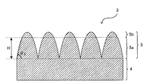
本発明における上記テーパー角度とは、本体部の縦断面での側面が直線状の場合、上記側面を近似する直線と、光透過性基板表面に平行な直線とで形成される角度をいい、例えば、図1(b)におけるθ1で表される角度である。
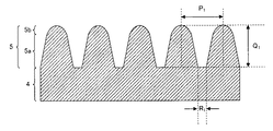
一方、本体部の縦断面での側面が曲線状の場合、本体部の頂面の外周上の点および本体部の底面の外周上の点を最短距離となるように選択して結んだ直線と、光透過性基板表面に平行な直線とで形成される角度をいい、例えば、図2におけるθ2で表される角度である。
ここで、本体部の頂面は、微細凹凸における凸部の側面の曲率が大きく変化する部位の横断面からなる面とし、本体部の底面は、本体部と基底部とが接する面とする。
なお、本発明における上記テーパー角度は、本体部の縦断面を電子顕微鏡により観察して10個分のテーパー角度を測定し、その測定値の平均値とする。また、図2は本発明における反射防止層の一例を示す概略断面図であり、図2における各符号については、図1(b)と同様であるので、ここでの記載は省略する。
The taper angle with respect to the light-transmitting substrate in the longitudinal section of the main body is not particularly limited as long as it is an angle capable of forming a truncated cone shape that rises in a tapered shape, but is 50 ° to 87 °. It is preferably within the range, more preferably within the range of 55 ° to 85 °, and even more preferably within the range of 55 ° to 82 °. When the taper angle is larger than the above range, the main body portion is close to a columnar shape that rises vertically, and may not be easily removed from the mold used in manufacturing the antireflection film of the present invention. This is because the antireflection function may not be exhibited. Furthermore, sticking may easily occur. On the other hand, when the taper angle is smaller than the above range, the antireflection function is lowered, the wavelength dependency of the reflectance is easily received, and it may be difficult to form the main body.
The taper angle in the present invention refers to an angle formed by a straight line approximating the side surface and a straight line parallel to the light-transmitting substrate surface when the side surface in the longitudinal section of the main body is linear. , An angle represented by θ 1 in FIG.
On the other hand, when the side surface in the longitudinal section of the main body is curved, the point on the outer periphery of the top surface of the main body and the point on the outer periphery of the bottom surface of the main body are selected and connected so as to be the shortest distance An angle formed by a straight line parallel to the surface of the light-transmitting substrate, for example, an angle represented by θ 2 in FIG.
Here, the top surface of the main body portion is a surface including a cross section of a portion where the curvature of the side surface of the convex portion in the fine unevenness greatly changes, and the bottom surface of the main body portion is a surface where the main body portion and the base portion are in contact.
The taper angle in the present invention is the average of the measured values obtained by observing the longitudinal section of the main body portion with an electron microscope and measuring the taper angle for ten pieces. FIG. 2 is a schematic cross-sectional view showing an example of the antireflection layer according to the present invention. Since the reference numerals in FIG. 2 are the same as those in FIG. 1B, description thereof is omitted here.
また、上記本体部の高さとしては、本発明における反射防止層に所望の反射防止機能を付与できる範囲内であれば特に限定されるものではなく、適宜調整できるものである。ここで、上記高さが高いほど、反射防止層の反射率を低くすることができ、一方、上記高さが低いほど、長波長側の反射率が増加する傾向にある。このようなことから、本発明における上記本体部の高さは、60nm〜1400nmの範囲内であることが好ましく、100nm〜1000nmの範囲内であることがより好ましく、120nm〜750nmの範囲内であることがさらに好ましい。本体部の高さが上記範囲よりも高いと、本体部が損壊しやすく、また、スティッキングが発生しやすくなる場合があり、本体部の高さが上記範囲よりも低いと、本発明における反射防止層の長波長側の光に対する反射防止機能が不十分になってしまう場合があるからである。
本発明における上記本体部の高さとは、基底部表面から、本体部の頂面までの距離をいい、例えば、図1(b)におけるHで表される距離である。なお、本発明における上記本体部の高さは、上述した方法で決定した平均値とする。
The height of the main body is not particularly limited as long as it is within a range in which a desired antireflection function can be imparted to the antireflection layer in the present invention, and can be adjusted as appropriate. Here, as the height is higher, the reflectance of the antireflection layer can be lowered. On the other hand, as the height is lower, the reflectance on the long wavelength side tends to increase. For this reason, the height of the main body in the present invention is preferably in the range of 60 nm to 1400 nm, more preferably in the range of 100 nm to 1000 nm, and in the range of 120 nm to 750 nm. More preferably. If the height of the main body portion is higher than the above range, the main body portion is likely to be damaged, and sticking may easily occur. If the height of the main body portion is lower than the above range, the antireflection in the present invention. This is because the antireflection function for light on the long wavelength side of the layer may be insufficient.
The height of the main body in the present invention refers to the distance from the base surface to the top surface of the main body, for example, a distance represented by H in FIG. In addition, let the height of the said main-body part in this invention be the average value determined by the method mentioned above.
上記本体部の頂面の径としては、上記本体部の底面の径よりも小さければ特に限定されるものではないが、1nm〜100nmの範囲内であることが好ましく、2nm〜50nmの範囲内であることがより好ましい。本体部の頂面の径が小さすぎると、機械的強度が小さくなり、本体部が損傷しやすくなるからである。また、本体部の頂面の径が大きすぎると、テーパーが小さくなるため、スティッキングを発生しやすくなったり、型から抜けにくくなったりするからである。なお、本発明における上記本体部の頂面の径は、上述した方法で決定した平均値とする。 The diameter of the top surface of the main body is not particularly limited as long as it is smaller than the diameter of the bottom of the main body, but is preferably in the range of 1 nm to 100 nm, and in the range of 2 nm to 50 nm. More preferably. This is because if the diameter of the top surface of the main body is too small, the mechanical strength is reduced and the main body is easily damaged. Moreover, if the diameter of the top surface of the main body is too large, the taper becomes small, so that sticking is likely to occur or it is difficult to remove from the mold. In addition, let the diameter of the top surface of the said main-body part in this invention be the average value determined by the method mentioned above.
上記本体部の底面の径としては、上記本体部の頂面の径よりも大きければ特に限定されるものではないが、25nm〜500nmの範囲内であることが好ましく、50nm〜250nmの範囲内であることがより好ましい。本体部の底面の径が小さくなると、隣り合う構造体の間が開き、構造体を形成していない部分が多くなるため、反射防止機能が悪くなる。なお、本発明における上記本体部の底面の径は、上述した方法で決定した平均値とする。 The diameter of the bottom surface of the main body is not particularly limited as long as it is larger than the diameter of the top surface of the main body, but is preferably in the range of 25 nm to 500 nm, and in the range of 50 nm to 250 nm. More preferably. When the diameter of the bottom surface of the main body portion is reduced, the space between adjacent structures is opened, and the portion not forming the structure is increased, so that the antireflection function is deteriorated. In addition, let the diameter of the bottom face of the said main-body part in this invention be the average value determined by the method mentioned above.
上記本体部の頂面形状および底面形状としては、特に限定されるものではなく、例えば、円、楕円等の丸形状の他、多角形形状などを挙げることができる。 The top surface shape and the bottom surface shape of the main body are not particularly limited, and examples thereof include a polygonal shape in addition to a circular shape such as a circle and an ellipse.
上記本体部の側面形状としては、上記本体部の縦断面において、直線状であってもよく、曲線状であってもよい。中でも、本発明においては、上記本体部が後述する先端部と連続的な曲面状の側面を形成することが好ましい。図2に例示するように、微細凹凸の凸部を釣鐘形状とすることができ、良好な反射防止機能を得ることができるからである。以下、上記凸部が釣鐘形状であることにより反射防止機能が良好となる理由について、具体的に説明する。 The side surface shape of the main body may be linear or curved in the longitudinal section of the main body. In particular, in the present invention, it is preferable that the main body portion forms a curved side surface that is continuous with a tip portion described later. This is because, as illustrated in FIG. 2, the convex portions of the fine irregularities can be formed into a bell shape, and a good antireflection function can be obtained. Hereinafter, the reason why the antireflection function is good when the convex portion has a bell shape will be specifically described.
モスアイ構造が反射防止をする原理については、次のように考えられる。図3(a)に例示されるモスアイ構造体Xの頂点部付近の空間(擬似層a)の屈折率Nは、空気の屈折率を1、擬似層a中でモスアイ構造体Xが占める体積の割合をVm、モスアイ構造体Xを構成する樹脂の屈折率をNmとすると、下記の(1)式が成り立つ。
N=1×(1−Vm)+Nm×Vm (1)
すなわち、擬似層aの屈折率は、空気と樹脂との、それぞれの体積と屈折率とを考慮した加重平均として与えられる。擬似層b以降も、同様である。擬似層a〜擬似層kへと基材Yに近づくにつれ、擬似層の屈折率は大きくなるが、図3(b)に例示するように、錐形状の屈折率の変化量が曲線的に変化するのに対して、釣鐘形状の屈折率の変化量はほぼ直線的に変化する。これは、モスアイ構造体Xが占める体積の割合は、擬似層aから擬似層kまでの断面積の変化ととらえることができ、この断面積の変化は錐形状の場合、曲線的に変化し、釣鐘形状の場合、ほぼ直線的に変化するからである。そのため、釣鐘形状のモスアイ構造体Xは、錐形状のモスアイ構造体Xに比べて、基材Y近傍の屈折率の変化率が小さいという特徴がある。基材Y近傍の屈折率の変化率が小さい方が、空気と樹脂との屈折率を小さくすることが擬似的に起こり、反射率を小さくすることが可能となる。また、本体部のテーパーが小さい場合、図3(b)に例示するように、擬似層kでの屈折率の変化量は小さいが、擬似層aからc部分での屈折率の変化量が大きくなるため、全体に白っぽくなる傾向がある。したがって、錐形状のモスアイ構造体Xおよびテーパーが小さい形状のモスアイ構造体Xよりも釣鐘形状のモスアイ構造体Xの方が、反射防止機能が優れている。
本発明においては、上記本体部のテーパー角度および上記先端部の曲率半径を適宜調整し、上記微細凹凸における凸部の釣鐘形状を規定することにより、上記擬似層の屈折率分布を最適化することができ、上記微細凹凸を光学的特性に優れたモスアイ構造とすることができる。
The principle that the moth-eye structure prevents reflection is considered as follows. The refractive index N of the space (pseudo layer a) near the apex of the moth eye structure X illustrated in FIG. 3A is 1 for the refractive index of air and the volume occupied by the moth eye structure X in the pseudo layer a. When the ratio is V m and the refractive index of the resin constituting the moth-eye structure X is N m , the following formula (1) is established.
N = 1 × (1−V m ) + N m × V m (1)
That is, the refractive index of the pseudo layer a is given as a weighted average considering the respective volumes and refractive indexes of air and resin. The same applies to the pseudo layer b and the subsequent layers. As the substrate Y approaches the pseudo layer a to the pseudo layer k, the refractive index of the pseudo layer increases. However, as illustrated in FIG. 3B, the amount of change in the refractive index of the cone shape changes in a curved manner. In contrast, the amount of change in the refractive index of the bell shape changes almost linearly. This is because the volume ratio occupied by the moth-eye structure X can be regarded as a change in the cross-sectional area from the pseudo layer a to the pseudo layer k. This is because the bell shape changes almost linearly. Therefore, the bell-shaped moth-eye structure X has a feature that the rate of change of the refractive index in the vicinity of the substrate Y is smaller than that of the cone-shaped moth-eye structure X. When the refractive index change rate in the vicinity of the substrate Y is smaller, the refractive index between the air and the resin is reduced in a pseudo manner, and the reflectance can be reduced. Further, when the taper of the main body is small, as shown in FIG. 3B, the amount of change in the refractive index in the pseudo layer k is small, but the amount of change in the refractive index in the portion from the pseudo layer a to c is large. Therefore, the whole tends to be whitish. Therefore, the bell-shaped moth-eye structure X is superior in antireflection function to the cone-shaped moth-eye structure X and the moth-eye structure X having a small taper.
In the present invention, the refractive index distribution of the pseudo layer is optimized by appropriately adjusting the taper angle of the main body part and the radius of curvature of the tip part and defining the bell shape of the convex part in the fine unevenness. Thus, the fine unevenness can be a moth-eye structure having excellent optical characteristics.
(b)先端部
本発明に用いられる先端部は、上記本体部の頂面を覆うように形成された曲面構造を有するものである。本発明においては、上記先端部が曲面構造を有することにより、反射防止層における微細凹凸パターンの凸部の最先端部が割れる等の不具合がなく、さらに、型抜き性に優れた反射防止フィルムとすることができる。なお、上記先端部の曲面構造は、反射防止層を形成する際の圧力、反射防止層の樹脂の粘度等で制御することが可能である。
(B) Tip portion The tip portion used in the present invention has a curved surface structure formed so as to cover the top surface of the main body portion. In the present invention, since the tip portion has a curved surface structure, there is no problem such as cracking of the leading edge of the convex portion of the fine unevenness pattern in the antireflection layer, and the antireflection film excellent in die-cutting property and can do. The curved surface structure of the tip portion can be controlled by the pressure when forming the antireflection layer, the viscosity of the resin of the antireflection layer, and the like.
上記先端部の形状としては、上記本体部の頂面を覆うように形成された曲面構造であれば特に限定されるものではない。本発明においては、中でも、略球面状であることが好ましく、その曲率半径としては、本発明の反射防止フィルムの用途等に応じて適宜調整することができるものであり、例えば、本発明に用いられる本体部の頂面の径に対して、1.0倍〜5.0倍の範囲内であることが好ましく、1.0倍〜2.0倍の範囲内であることがより好ましく、1.0倍〜1.5倍の範囲内であることがさらに好ましい。先端部の曲率半径が上記範囲よりも大きいと、先端部が平らな形状に近くなるため、反射防止層の反射率が高くなり、本発明の反射防止フィルムの反射防止機能が低下する場合があるからである。また、図4(a)に例示するように、先端部5bの曲面構造は、球面状であることが望ましいが、図4(b)、(c)に例示するように、先端部5bの曲面構造は、一部尖っている形状および/またはうねりがあってもよい。また、先端部の最先端部は本体部の頂面の中心にある必要はなく、中心からずれていても反射防止機能には変化はない。なお、図4(a)〜(c)は、本発明の反射防止フィルムにおける先端部の一例を示す概略断面図である。
The shape of the tip is not particularly limited as long as it is a curved structure formed so as to cover the top surface of the main body. In the present invention, in particular, it is preferably substantially spherical, and the radius of curvature thereof can be appropriately adjusted according to the application of the antireflection film of the present invention, for example, used in the present invention. The diameter of the top surface of the main body is preferably within a range of 1.0 to 5.0 times, more preferably within a range of 1.0 to 2.0 times. More preferably, it is in the range of 0.0 times to 1.5 times. If the curvature radius of the tip portion is larger than the above range, the tip portion becomes close to a flat shape, so that the reflectance of the antireflection layer increases, and the antireflection function of the antireflection film of the present invention may deteriorate. Because. Further, as illustrated in FIG. 4A, the curved surface structure of the
また、上記先端部の高さ、すなわち、本体部の頂面から先端部の最先端部までの距離としては、本発明における反射防止層に所望の反射防止機能を付与できる範囲内で適宜調整することができるものである。 Further, the height of the tip portion, that is, the distance from the top surface of the main body portion to the most distal portion of the tip portion is appropriately adjusted within a range in which a desired antireflection function can be imparted to the antireflection layer in the present invention. It is something that can be done.
(c)凸部
本発明に用いられる凸部は、上記先端部と上記本体部とから構成されるものであり、本発明における反射防止層が備える反射防止機能は、上記凸部が形成された周期、高さ、間隔に依存する。
なお、上記凸部が形成された周期、高さ、および間隔は、それぞれ図5におけるP1、Q1、およびR1で示す通り、それぞれ隣接する凸部における先端部の頂部から先端部の頂部までの距離、凸部における先端部の頂部から本体部の底面までの距離、および隣接する凸部における本体部の底面の外周間の最短距離である。ここで、図5は本発明の反射防止フィルムにおける微細凹凸を特定するパラメーターを説明する概略図であり、図5において説明していない符号については、図1(b)と同様とすることができるので、ここでの記載は省略する。
(C) Convex part The convex part used for this invention is comprised from the said front-end | tip part and the said main-body part, and the antireflection function with which the antireflection layer in this invention is provided has the said convex part. Depends on period, height, interval.
The period of the convex portion is formed, a height, and spacing, P 1, Q 1, and as shown by R 1, the top portion of the tip portion from the top of the front end portion of the raised portion adjacent each respectively, in FIG 5 , The distance from the top of the tip of the protrusion to the bottom of the main body, and the shortest distance between the outer peripheries of the bottom of the main body of the adjacent protrusion. Here, FIG. 5 is a schematic diagram for explaining parameters for specifying fine irregularities in the antireflection film of the present invention. Reference numerals not described in FIG. 5 can be the same as those in FIG. Therefore, the description here is omitted.
上記凸部の周期としては、可視光領域の波長以下であれば特に限定されるものではなく、本発明の反射防止フィルムの用途等に応じて適宜決定することができる。ここで、上記周期は、本発明に用いられる反射防止層の反射率の波長依存性に影響を及ぼすものであり、その周期が長くなるほど可視光領域の短波長側の光に対する反射率が増加する傾向にある。一方、周期が200nm以下においては、周期の変動に伴う反射率の波長依存性の変化は少なくなるものである。このようなことから、本発明における上記凸部の周期は、80nm〜400nmの範囲内であることが好ましく、100nm〜300nmの範囲内であることがより好ましく、120nm〜250nmの範囲内であることがさらに好ましい。上記凸部の周期が上記範囲よりも短いと、個々の凸部の形状が極微小になることから、高精度で凸部を形成することが困難になる場合があるからである。また、上記凸部の周期が上記範囲よりも長いと、本発明における反射防止層の短波長側の光に対する反射防止機能が不十分になってしまう場合があるからである。なお、本発明における上記凸部の周期は、凸部の縦断面を電子顕微鏡により観察して10個分の周期を測定し、その測定値の平均値とする。 The period of the convex portion is not particularly limited as long as it is equal to or shorter than the wavelength of the visible light region, and can be appropriately determined according to the use of the antireflection film of the present invention. Here, the period affects the wavelength dependence of the reflectance of the antireflection layer used in the present invention, and the reflectance for light on the short wavelength side in the visible light region increases as the period becomes longer. There is a tendency. On the other hand, when the period is 200 nm or less, the change in the wavelength dependence of the reflectance due to the fluctuation of the period is small. For this reason, the period of the convex portions in the present invention is preferably in the range of 80 nm to 400 nm, more preferably in the range of 100 nm to 300 nm, and in the range of 120 nm to 250 nm. Is more preferable. This is because if the period of the convex portions is shorter than the above range, the shape of the individual convex portions becomes extremely small, so that it may be difficult to form the convex portions with high accuracy. Further, if the period of the convex portion is longer than the above range, the antireflection function for light on the short wavelength side of the antireflection layer in the present invention may be insufficient. In addition, the period of the said convex part in this invention observes the longitudinal cross-section of a convex part with an electron microscope, measures the period for ten pieces, and makes it the average value of the measured value.
上記凸部の高さについても、本発明における反射防止層に所望の反射防止機能を付与できる範囲内で適宜調整することができるものであり、特に限定されるものではない。ここで、上記高さが高いほど、反射防止層の反射率を低くすることができ、一方、低くなると長波長側の反射率が増加する傾向にある。このようなことから、本発明における上記凸部の高さは、62nm〜1402nmの範囲内であることが好ましく、100nm〜1002nmの範囲内であることがより好ましく、120nm〜752nmの範囲内であることがさらに好ましい。上記凸部の高さが上記範囲よりも高いと、個々の凸部が損壊しやすくなってしまう場合があり、上記凸部の高さが上記範囲よりも低いと、本発明における反射防止層の長波長側の光に対する反射防止機能が不十分になってしまう場合があるからである。なお、本発明における上記凸部の高さは、上述した方法で決定した平均値とする。 The height of the convex portion can be appropriately adjusted within a range in which a desired antireflection function can be imparted to the antireflection layer in the invention, and is not particularly limited. Here, as the height is higher, the reflectance of the antireflection layer can be lowered. On the other hand, when the height is lowered, the reflectance on the long wavelength side tends to increase. Therefore, the height of the convex portion in the present invention is preferably in the range of 62 nm to 1402 nm, more preferably in the range of 100 nm to 1002 nm, and in the range of 120 nm to 752 nm. More preferably. If the height of the convex portion is higher than the above range, the individual convex portions may be easily damaged, and if the height of the convex portion is lower than the above range, the antireflection layer of the present invention This is because the antireflection function for light on the long wavelength side may be insufficient. In addition, the height of the said convex part in this invention is taken as the average value determined by the method mentioned above.
上記凸部が形成された間隔は、広くなるほど可視光の全波長領域において反射率が増加する傾向にあり、狭くなるほど可視光の全波長領域において反射率が低下する傾向にある。このようなことから、本発明における上記凸部が形成された間隔は、本発明における反射防止層に所望の反射防止機能を付与できる範囲内で適宜調整することができるものであり、特に限定されるものではない。なお、本発明における上記凸部の間隔は、上述した方法で決定した平均値とする。 As the interval at which the convex portions are formed increases, the reflectance tends to increase in the entire wavelength region of visible light, and as the interval decreases, the reflectance tends to decrease in the entire wavelength region of visible light. For this reason, the interval at which the convex portions are formed in the present invention can be appropriately adjusted within a range in which a desired antireflection function can be imparted to the antireflection layer in the present invention, and is particularly limited. It is not something. In addition, the space | interval of the said convex part in this invention is taken as the average value determined by the method mentioned above.
上記凸部の高さのばらつきとしては、100nm以下であることが好ましく、50nm以下であることがより好ましく、10nm以下であることがさらに好ましい。上記凸部の高さのばらつきが上記範囲よりも大きいと、本発明における反射防止層の反射防止機能にムラが生じる場合があるからである。また、凸部の頂点から構成される表面の機械的強度が低下し、損傷を受けやすくなる。なお、上記凸部の高さのばらつきとは、凸部の縦断面を電子顕微鏡により観察して10個分の高さを測定し、その測定値の最大値と最小値との差をいう。 The variation in the height of the protrusions is preferably 100 nm or less, more preferably 50 nm or less, and even more preferably 10 nm or less. This is because if the variation in the height of the convex portions is larger than the above range, unevenness may occur in the antireflection function of the antireflection layer in the present invention. Moreover, the mechanical strength of the surface comprised from the vertex of a convex part falls, and it becomes easy to receive a damage. In addition, the variation in the height of the convex portion means a difference between the maximum value and the minimum value of the measured values obtained by observing the vertical section of the convex portion with an electron microscope and measuring the height of ten pieces.
上記凸部の単位面積当たりの個数としては、本発明における反射防止層に所望の反射防止機能を付与できる範囲内で適宜調整することができるものであり、特に限定されるものではないが、例えば、50個/μm2以上であることが好ましく、60個/μm2以上であることがより好ましく、70個/μm2以上であることがさらに好ましい。上記凸部の単位面積当たりの個数が50個/μm2以下の場合、ギラツキが発生し、反射防止機能が悪くなる。また、凸部の頂点から構成される表面の機械的強度が低下し、損傷を受けやすくなる。
なお、本発明においては、反射防止層が上記凸部以外の構造体を有していてもよいが、反射防止層における上記凸部の個数の、反射防止層における構造体全体の個数に対する割合は、50%以上であることが好ましく、60%以上であることがより好ましく、75%以上であることがさらに好ましい。上記割合が少なすぎると、反射防止機能、スティッキング耐性および型抜け性が低下してしまうからである。
The number of convex portions per unit area can be appropriately adjusted within a range in which a desired antireflection function can be imparted to the antireflection layer in the present invention, and is not particularly limited. 50 / μm 2 or more, preferably 60 / μm 2 or more, and more preferably 70 / μm 2 or more. If the number of the convex portions per unit area is 50 / μm 2 or less, glare occurs and the antireflection function deteriorates. Moreover, the mechanical strength of the surface comprised from the vertex of a convex part falls, and it becomes easy to receive a damage.
In the present invention, the antireflection layer may have a structure other than the protrusions, but the ratio of the number of protrusions in the antireflection layer to the total number of structures in the antireflection layer is 50% or more, more preferably 60% or more, and even more preferably 75% or more. This is because if the ratio is too small, the antireflection function, the sticking resistance and the mold release property are lowered.
上記凸部の360nm〜760nmの波長領域における入射角5°での正反射率は、0.5%以下であることが好ましく、0.005%〜0.3%の範囲内であることがより好ましく、0.005%〜0.1%の範囲内であることがさらに好ましい。
また、上記凸部の360nm〜760nmの波長領域におけるヘイズ値は、0.1%〜50%の範囲内であることが好ましい。
The regular reflectance at an incident angle of 5 ° in the wavelength region of 360 nm to 760 nm of the convex portion is preferably 0.5% or less, and more preferably in the range of 0.005% to 0.3%. Preferably, it is more preferably in the range of 0.005% to 0.1%.
Moreover, it is preferable that the haze value in the 360 nm-760 nm wavelength range of the said convex part exists in the range of 0.1%-50%.
上記凸部は、短波長領域から長波長領域までくまなく反射することが可能である。 The convex portion can reflect all over from a short wavelength region to a long wavelength region.
(2)基底部
本発明に用いられる反射防止層における基底部は、上記易接着層上に形成され、上記微細凹凸を支持するものである。
上記基底部の厚みとしては、0.5μm〜150μmの範囲内であることが好ましく、1μm〜100μmの範囲内であることがより好ましく、2μm〜80μmの範囲内であることがさらに好ましい。基底部の厚みが上記範囲内であることにより、反射防止層の収縮応力の程度を低減することができ、上記易接着層および後述する光透過性基板等の種類に関わらず、本発明の反射防止フィルムにカールが生じることを防止することができるからである。また、クッション層としての効果があり、反射防止層の機械的損傷を補強することができる。例えば、反射防止層の機械的強度を高くさせたり、擦傷耐性を向上させ、傷つきにくくさせたりすることができる。さらに、反射防止層と易接着層との密着性を向上させることができる。
(2) Base part The base part in the antireflection layer used for this invention is formed on the said easily bonding layer, and supports the said fine unevenness | corrugation.
The thickness of the base is preferably in the range of 0.5 μm to 150 μm, more preferably in the range of 1 μm to 100 μm, and still more preferably in the range of 2 μm to 80 μm. When the thickness of the base portion is within the above range, the degree of shrinkage stress of the antireflection layer can be reduced, and the reflection of the present invention is performed regardless of the kind of the easily adhesive layer and the light-transmitting substrate described later. This is because curling can be prevented from occurring in the prevention film. Moreover, there exists an effect as a cushion layer and it can reinforce the mechanical damage of an antireflection layer. For example, the mechanical strength of the antireflection layer can be increased, scratch resistance can be improved, and scratch resistance can be reduced. Furthermore, the adhesion between the antireflection layer and the easy-adhesion layer can be improved.
(3)反射防止層
本発明における反射防止層は、通常、樹脂からなるものである。反射防止層に用いられる樹脂としては、上述した微細凹凸を形成できるものであれば特に限定されるものではなく、紫外線硬化性樹脂や電子線硬化性樹脂等の電離放射線硬化性樹脂、熱硬化性樹脂、熱可塑性樹脂等を挙げることができる。中でも、本発明においては、電離放射線硬化性樹脂を用いることが好ましい。電離線放射線硬化性樹脂を用いることで、高精度に微細凹凸を作製することができ、反射防止層に良好な反射防止機能を付与することができるからである。
(3) Antireflection layer The antireflection layer in the present invention is usually made of a resin. The resin used for the antireflection layer is not particularly limited as long as it can form the fine irregularities described above. Ionizing radiation curable resins such as ultraviolet curable resins and electron beam curable resins, and thermosetting. Examples thereof include resins and thermoplastic resins. Among these, in the present invention, it is preferable to use an ionizing radiation curable resin. This is because by using the ionizing radiation curable resin, fine irregularities can be produced with high accuracy, and a good antireflection function can be imparted to the antireflection layer.
本発明に用いられる電離放射線硬化性樹脂としては、例えば、アクリル系樹脂が挙げられる。アクリル系樹脂としては、少なくとも3つ以上のエチレン性不飽和二重結合を有する化合物を挙げることができる。例えば、ペンタエリスリトールトリ(メタ)アクリレート、ペンタエリスリトールテトラ(メタ)アクリレート、トリメチロールプロパントリ(メタ)アクリレート、EO変性トリメチロールプロパントリ(メタ)アクリレート、PO変性トリメチロールプロパントリ(メタ)アクリレート、トリス(アクリロキシエチル)イソシアヌレート、カプロラクトン変性トリス(アクリロキシエチル)イソシアヌレート、トリメチロールエタントリ(メタ)アクリレート、ジペンタエリスリトールテトラ(メタ)アクリレート、ジペンタエリスリトールペンタ(メタ)アクリレート、ジペンタエリスリトールヘキサ(メタ)アクリレート、アルキル変性ジペンタエリスリトールトリ(メタ)アクリレート、アルキル変性ジペンタエリスリトールテトラ(メタ)アクリレート、アルキル変性ジペンタエリスリトールペンタ(メタ)アクリレート、カプロラクトン変性ジペンタエリスリトールヘキサ(メタ)アクリレート、1,2,3−シクロヘキサンテトラ(メタ)アクリレート、ポリウレタンポリアクリレート、ポリエステルポリアクリレート等の多価アルコールと(メタ)アクリル酸とのエステル化合物;ポリウレタンポリ(メタ)アクリレート、ポリエステルポリ(メタ)アクリレート、ポリエーテルポリ(メタ)アクリレート、ポリアクリルポリ(メタ)アクリレート、ポリアルキッドポリ(メタ)アクリレート、ポリエポキシポリ(メタ)アクリレート、ポリスピロアセタールポリ(メタ)アクリレート、ポリブタジエンポリ(メタ)アクリレート、ポリチオールポリエンポリ(メタ)アクリレート、ポリシリコンポリ(メタ)アクリレート等の多官能化合物の(メタ)アクリレート化合物等が挙げられる。
これら少なくとも3つ以上のエチレン性不飽和二重結合を有する化合物のうち、塗膜強度、密着性の観点より、少なくとも6つの官能基を有するポリウレタンポリ(メタ)アクリレート、ポリエポキシポリ(メタ)アクリレート等のポリ(メタ)アクリレート類、分子内に4個以上のアクリロイル基を有する多官能のアクリレート類を好適に使用することができる。
ポリウレタンポリ(メタ)アクリレートは、例えば、ジイソシアネートと水酸基を有する(メタ)アクリレート類と反応させて得られるもの、ポリオールとポリイソシアネートとをイソシアネート基過剰の条件下に反応させてなるイソシアネート基含有ウレタンプレポリマーを、水酸基を有する(メタ)アクリレート類と反応させて得られるものがある。あるいは、ポリオールとポリイソシアネートとを水酸基過剰の条件下に反応させてなる水酸基含有ウレタンプレポリマーを、イソシアネート基を有する(メタ)アクリレート類と反応させて得ることもできる。
ポリオールとしては、エチレングリコール、プロピレングリコール、ジエチレングリコール、ジプロピレングリコール、ブチレングリコール、1,6−ヘキサンジオール、3−メチル−1,5−ペンタングリコール、ネオペンチルグリコール、ヘキサントリオール、トリメリロールプロパン、ポリテトラメチレングリコール、アジピン酸とエチレングリコールとの縮重合物等が挙げられる。
ポリイソシアネートとしては、トリレンジイソシアネート、イソホロンジイソシアネート、ヘキサメチレンジイソシアネート等が挙げられる。
水酸基をもつ(メタ)アクリレート類としては、2−ヒドロキシエチルアクリレート、2−ヒドロキシプロピルアクリテート、4−ヒドロキシブチルアクリレート、ペンタエリスリトールトリアクリレート、ジペンタエリスリトールペンタアクリレート、ジトリメチロールプロパンテトラアクリレート等が挙げられる。
イソシアネート基を有する(メタ)アクリレート類としては、2−メタクリロイルオキシエチルイソシアネート、メタクリロイルイソシアネート等が挙げられる。
ポリエポキシポリ(メタ)アクリレートは、エポキシ樹脂のエポキシ基を(メタ)アクリル酸でエステル化し、官能基を(メタ)アクリロイル基としたものであり、ビスフェノールA型エポキシ樹脂への(メタ)アクリル酸付加物、ノボラック型エポキシ樹脂への(メタ)アクリル酸付加物等がある。
分子内に4個以上のアクリロイル基を有する多官能としては、具体的には、上述した多価アルコールとアクリル酸のエステル化合物が挙げられ、単独または2種以上の混合物が好ましい。
さらに、WO2007/040159に記載されている(メタ)アクリル系重合性組成物を用いることができる。
また、上記樹脂には、光重合開始剤を適宜添加することが望ましい。光重合開始剤としては、例えば、アセトフェノン類、ベンゾイン類、ベンゾフェノン類、ホスフィンオキシド類、ケタール類、アントラキノン類、チオキサントン類等が挙げられる。具体的には、ベンゾインメチルエーテル、ベンゾインエチルエーテル、ベンゾインイソプロピルエーテル、ベンゾインブチルエーテル、ジエトキシアセトフェノン、ゲンジルジメチルケタール、2−ヒドロキシ−2−メチルプロピオフェノン、1−ヒドロキシシクロヘキシルフェニルケトン、ベンゾフェノン、2,4,6−トリメチルベンゾインジフェニルホスフィンオキシド、ミヒラーズケトン、N,N−ジメチルアミノ安息香酸イソアミル、2−クロロチオキサントン、2,4−ジエチルチオキサントン等が挙げられ、これらの光重合開始剤は2種以上を適宜併用することもできる。
本発明においては、これらの電離放射線硬化性樹脂の中から、後述する光透過性基板の屈折率と近い屈折率を有する樹脂を適宜選択して用いることが好ましい。易接着層の屈折率を、反射防止層の屈折率および光透過性基板の屈折率に近づけることができるからである。
Examples of the ionizing radiation curable resin used in the present invention include acrylic resins. Examples of the acrylic resin include compounds having at least three ethylenically unsaturated double bonds. For example, pentaerythritol tri (meth) acrylate, pentaerythritol tetra (meth) acrylate, trimethylolpropane tri (meth) acrylate, EO modified trimethylolpropane tri (meth) acrylate, PO modified trimethylolpropane tri (meth) acrylate, tris (Acryloxyethyl) isocyanurate, caprolactone-modified tris (acryloxyethyl) isocyanurate, trimethylol ethane tri (meth) acrylate, dipentaerythritol tetra (meth) acrylate, dipentaerythritol penta (meth) acrylate, dipentaerythritol hexa (Meth) acrylate, alkyl-modified dipentaerythritol tri (meth) acrylate, alkyl-modified dipentaerythritol tet (Meth) acrylate, alkyl-modified dipentaerythritol penta (meth) acrylate, caprolactone-modified dipentaerythritol hexa (meth) acrylate, 1,2,3-cyclohexanetetra (meth) acrylate, polyurethane polyacrylate, polyester polyacrylate, etc. Ester compound of monohydric alcohol and (meth) acrylic acid; polyurethane poly (meth) acrylate, polyester poly (meth) acrylate, polyether poly (meth) acrylate, polyacryl poly (meth) acrylate, polyalkyd poly (meth) acrylate , Polyepoxy poly (meth) acrylate, polyspiroacetal poly (meth) acrylate, polybutadiene poly (meth) acrylate, polythiol polyene poly ( Data) acrylate, (meth) acrylate compound of the polysilicon poly (meth) polyfunctional compounds such acrylate.
Among these compounds having at least three or more ethylenically unsaturated double bonds, polyurethane poly (meth) acrylate and polyepoxy poly (meth) acrylate having at least six functional groups from the viewpoint of coating film strength and adhesion. Poly (meth) acrylates such as polyfunctional acrylates having 4 or more acryloyl groups in the molecule can be suitably used.
The polyurethane poly (meth) acrylate is obtained by reacting, for example, a diisocyanate and a (meth) acrylate having a hydroxyl group, or an isocyanate group-containing urethane prepolymer obtained by reacting a polyol and a polyisocyanate under an excess of isocyanate groups. Some are obtained by reacting polymers with (meth) acrylates having a hydroxyl group. Alternatively, a hydroxyl group-containing urethane prepolymer obtained by reacting a polyol and a polyisocyanate under hydroxyl-excess conditions can be obtained by reacting with a (meth) acrylate having an isocyanate group.
Examples of polyols include ethylene glycol, propylene glycol, diethylene glycol, dipropylene glycol, butylene glycol, 1,6-hexanediol, 3-methyl-1,5-pentane glycol, neopentyl glycol, hexanetriol, trimellilol propane, polytetra Examples include methylene glycol and a condensation polymer of adipic acid and ethylene glycol.
Examples of the polyisocyanate include tolylene diisocyanate, isophorone diisocyanate, and hexamethylene diisocyanate.
Examples of (meth) acrylates having a hydroxyl group include 2-hydroxyethyl acrylate, 2-hydroxypropyl acrylate, 4-hydroxybutyl acrylate, pentaerythritol triacrylate, dipentaerythritol pentaacrylate, and ditrimethylolpropane tetraacrylate. .
Examples of (meth) acrylates having an isocyanate group include 2-methacryloyloxyethyl isocyanate and methacryloyl isocyanate.
Polyepoxy poly (meth) acrylate is obtained by esterifying an epoxy group of an epoxy resin with (meth) acrylic acid and converting the functional group to a (meth) acryloyl group, and (meth) acrylic acid to bisphenol A type epoxy resin There are adducts, (meth) acrylic acid adducts to novolac type epoxy resins, and the like.
Specific examples of the polyfunctional group having four or more acryloyl groups in the molecule include the above-described polyhydric alcohol and acrylic acid ester compounds, and a single compound or a mixture of two or more compounds is preferable.
Furthermore, a (meth) acrylic polymerizable composition described in WO2007 / 040159 can be used.
Moreover, it is desirable to add a photopolymerization initiator to the resin as appropriate. Examples of the photopolymerization initiator include acetophenones, benzoins, benzophenones, phosphine oxides, ketals, anthraquinones, thioxanthones, and the like. Specifically, benzoin methyl ether, benzoin ethyl ether, benzoin isopropyl ether, benzoin butyl ether, diethoxyacetophenone, gendyl dimethyl ketal, 2-hydroxy-2-methylpropiophenone, 1-hydroxycyclohexyl phenyl ketone, benzophenone, 2 , 4,6-trimethylbenzoin diphenylphosphine oxide, Michler's ketone, isoamyl N, N-dimethylaminobenzoate, 2-chlorothioxanthone, 2,4-diethylthioxanthone, and the like. It can also be used together as appropriate.
In the present invention, it is preferable to appropriately select and use a resin having a refractive index close to the refractive index of a light-transmitting substrate described later from among these ionizing radiation curable resins. This is because the refractive index of the easy adhesion layer can be made close to the refractive index of the antireflection layer and the refractive index of the light-transmitting substrate.
また、本発明に用いられる熱硬化性樹脂あるいは熱可塑性樹脂としては、例えば、アクリル樹脂、ポリエステル樹脂、エポキシ樹脂、ポリオレフィン樹脂、スチロール樹脂、ポリアミド樹脂、ポリイミド樹脂、ポリアミドイミド樹脂、ポリウレタン樹脂、ポリ酢酸ビニル樹脂、ポリビニルアルコール樹脂、ポリビニルブチラール樹脂、ポリカーボネート樹脂、メラミン樹脂、尿素樹脂、アルキッド樹脂、フェノール樹脂、セルロース樹脂、ジアリルフタレート樹脂、シリコーン樹脂、ポリアリレート樹脂、ポリアセタール樹脂、スチレン−イソプレンゴム、オレフィン・マレイミド共重合体、フルオレイン系エポキシ、フルオレイン系アクリレート、フルオレイン系ポリエステル、フッ素樹脂等を挙げることができる。また、これらのエラストマーや酸変性物などを挙げることができる。 Examples of the thermosetting resin or thermoplastic resin used in the present invention include acrylic resin, polyester resin, epoxy resin, polyolefin resin, styrene resin, polyamide resin, polyimide resin, polyamideimide resin, polyurethane resin, and polyacetic acid. Vinyl resin, polyvinyl alcohol resin, polyvinyl butyral resin, polycarbonate resin, melamine resin, urea resin, alkyd resin, phenol resin, cellulose resin, diallyl phthalate resin, silicone resin, polyarylate resin, polyacetal resin, styrene-isoprene rubber, olefin Menimide copolymers, fluorinated epoxies, fluorinated acrylates, fluorinated polyesters, fluororesins and the like can be mentioned. Moreover, these elastomers and acid-modified products can be mentioned.
本発明における反射防止層の透明度としては、可視光の全波長範囲に対する光の透過率が80%以上であることが好ましく、85%以上であることがより好ましく、90%以上であることがさらに好ましい。
ここで、上記光の透過率は、例えば、株式会社日立ハイテクノロジーズ製分光光度計、U−4100により測定することができる。
As the transparency of the antireflection layer in the present invention, the light transmittance with respect to the entire wavelength range of visible light is preferably 80% or more, more preferably 85% or more, and further preferably 90% or more. preferable.
Here, the light transmittance can be measured by, for example, a spectrophotometer U-4100 manufactured by Hitachi High-Technologies Corporation.
本発明に用いられる反射防止層の反射防止機能は、反射防止層の屈折率および上記易接着層の屈折率にも依存するものである。すなわち、反射防止層の屈折率と、上記易接着層の屈折率との差が小さいほど、屈折率の不連続性を是正することができるため、反射防止層の反射防止機能を向上させることができるものである。このような観点から、本発明においては、反射防止層の屈折率と、上記易接着層の屈折率との差は、0〜0.5の範囲内であることが好ましく、0〜0.2の範囲内であることがより好ましく、0〜0.1の範囲内であることがさらに好ましい。反射防止層の具体的な屈折率の値は、特に限定されるものではないが、上記易接着層の屈折率との差が小さいことが好ましいことから、後述する光透過性基板の屈折率に近いことが好ましく、通常、1.20〜2.40の範囲内とされる。 The antireflection function of the antireflection layer used in the present invention depends on the refractive index of the antireflection layer and the refractive index of the easy-adhesion layer. That is, the smaller the difference between the refractive index of the antireflection layer and the refractive index of the easy-adhesion layer, the more the discontinuity of the refractive index can be corrected. Therefore, the antireflection function of the antireflection layer can be improved. It can be done. From such a viewpoint, in the present invention, the difference between the refractive index of the antireflection layer and the refractive index of the easy-adhesion layer is preferably in the range of 0 to 0.5, and preferably 0 to 0.2. More preferably, it is in the range of 0 to 0.1. Although the specific refractive index value of the antireflection layer is not particularly limited, since it is preferable that the difference from the refractive index of the easy-adhesion layer is small, the refractive index of the light-transmitting substrate described later is used. It is preferable that they are close to each other, and usually within a range of 1.20 to 2.40.
本発明に用いられる反射防止層は、上述した樹脂に加えて、必要に応じて任意の添加剤を含有していてもよい。このような添加剤としては、上記「1.易接着層」の項に記載した添加剤と同様のものを用いることができるので、ここでの記載は省略する。 The antireflection layer used in the present invention may contain any additive as necessary in addition to the above-described resin. As such an additive, the same additive as the additive described in the section of “1. Easy-adhesion layer” can be used, and the description thereof is omitted here.
3.光透過性基板
次に、本発明における光透過性基板について説明する。本発明における光透過性基板は、ポリエチレンテレフタレート(PET)樹脂からなるものである。また、上記光透過性基板は、上述した易接着層および反射防止層を支持するものであり、上記易接着層および反射防止層と相まって、本発明の反射防止フィルムに所望の反射防止機能を付与するものである。
3. Next, the light transmissive substrate in the present invention will be described. The light-transmitting substrate in the present invention is made of polyethylene terephthalate (PET) resin. The light-transmitting substrate supports the above-mentioned easy adhesion layer and antireflection layer, and in combination with the above easy adhesion layer and antireflection layer, imparts a desired antireflection function to the antireflection film of the present invention. To do.
また、本発明における光透過性基板は、可視光に対する透過性を備えるものであり、中でも、可視光の全波長範囲に対する光の透過率が80%以上であることが好ましく、85%以上であることがより好ましく、90%以上であることがさらに好ましい。
ここで、上記光の透過率は、例えば、株式会社日立ハイテクノロジーズ製分光光度計、U−4100により測定することができる。
Further, the light-transmitting substrate in the present invention has transparency to visible light, and in particular, the light transmittance for the entire wavelength range of visible light is preferably 80% or more, and 85% or more. More preferably, it is more preferably 90% or more.
Here, the light transmittance can be measured by, for example, a spectrophotometer U-4100 manufactured by Hitachi High-Technologies Corporation.
本発明における光透過性基板の屈折率は、ほぼ一定であり、通常、1.57〜1.59程度である。 The refractive index of the light-transmitting substrate in the present invention is substantially constant, and is usually about 1.57 to 1.59.
本発明における光透過性基板は、PET樹脂からなるものであるが、必要に応じて任意の添加剤を含有していてもよい。このような添加剤としては、例えば、帯電防止剤(導電剤)、屈折率調整剤、レベリング剤、防汚染剤、粘着剤、紫外線・赤外線吸収剤、高硬度化剤、硬度調整剤、流動性調整剤、酸化防止剤、フッ素系樹脂、流動パラフィン、パラフィンワックス、合成ポリエチレンワックスなどの炭化水素系、脂肪酸アマイド系、ステアリン酸金属塩、ステアリン酸カルシウム・ステアリン酸マグネシウム、ステアリン酸鉛・ステアリン酸亜鉛などの金属石鹸系、脂肪酸エステル系、シリコーンオイル系、アクリル系高分子系などの離型剤や内部または外部滑剤、炭酸ストロンチウムなどの偏屈折調整剤、親水性剤、親油性剤、着色剤等を挙げることができる。 The light-transmitting substrate in the present invention is made of a PET resin, but may contain any additive as necessary. Examples of such additives include antistatic agents (conductive agents), refractive index adjusters, leveling agents, antifouling agents, adhesives, ultraviolet / infrared absorbers, hardeners, hardness adjusters, and fluidity. Conditioners, antioxidants, fluororesins, hydrocarbons such as liquid paraffin, paraffin wax, synthetic polyethylene wax, fatty acid amides, metal stearate, calcium stearate / magnesium stearate, lead stearate / zinc stearate, etc. Release agents such as metal soaps, fatty acid esters, silicone oils, acrylic polymers, internal or external lubricants, polarization refraction regulators such as strontium carbonate, hydrophilic agents, lipophilic agents, colorants, etc. Can be mentioned.
本発明における光透過性基板の厚みとしては、上述した易接着層および反射防止層を支持することができれば特に限定されるものではなく、本発明の反射防止フィルムに応じて適宜選択することができるものであるが、1μm〜1000μmの範囲内であることが好ましく、5μm〜500μmの範囲内であることがより好ましい。 The thickness of the light transmissive substrate in the present invention is not particularly limited as long as it can support the above-mentioned easy adhesion layer and antireflection layer, and can be appropriately selected according to the antireflection film of the present invention. However, it is preferably in the range of 1 μm to 1000 μm, and more preferably in the range of 5 μm to 500 μm.
4.反射防止フィルム
本発明の反射防止フィルムは、図1(a)に例示するように、光透過性基板1上に、易接着層2および反射防止層3が順に形成された構造であってもよく、図6に例示するように、光透過性基板1を挟むように易接着層2および反射防止層3が順に形成された構造であってもよい。なお、図6は本発明の反射防止フィルムの他の例を示す概略断面図であり、図6において説明していない符号については、図1(a)と同様とすることができるので、ここでの記載は省略する。
4). Antireflection Film The antireflection film of the present invention may have a structure in which an easy-
また、本発明の反射防止フィルムは、少なくとも上記反射防止層と、上記易接着層と、上記光透過性基板とを有するものであるが、必要に応じて任意の構成が用いられていてもよい。本発明に用いられる任意の構成は、特に限定されるものではなく、本発明の反射防止フィルムの用途等に応じて、所望の機能を付与することができる構成を適宜選択して用いることができる。中でも、本発明に好適に用いられる任意の構成としては、上記易接着層と、上記反射防止層との間に形成されるプライマー層(密着安定層)、ハードコート層、帯電防止層等の機能層、および、上記光透過性基板の上記易接着層および上記反射防止層が形成された面とは反対の面上に形成される粘着層を挙げることができる。プライマー層は、ハードコート層および/または帯電防止層を兼ねることもできる。また、反射防止層の表面に形成される保護層を用いることもできる。
ここで、上記機能層としてハードコート層が形成されていることにより、本発明の反射防止フィルムの硬度を向上させ、耐久性に優れた反射防止フィルムとすることができることから、本発明の反射防止フィルムを表示装置に用いた場合に、本発明の反射防止フィルムを表示装置の保護フィルムとして用いることも可能になるという利点がある。また、上記機能層としてプライマー層が形成されていることにより、易接着層と反射防止層との密着性を向上させ、易接着層およびプライマー層を介して、反射防止層と光透過性基板との密着性をより向上させることができ、上記機能層として帯電防止層が形成されていることにより、静電気の発生を抑制し、本発明の反射防止フィルムへの埃や汚れの付着を防止することができる。
一方、上記粘着層が形成されていることにより、例えば、本発明の反射防止フィルムを表示装置に用いる場合に、本発明の反射防止フィルムを他の部材に貼り合わせることが容易になるという利点がある。
Moreover, although the antireflection film of the present invention has at least the antireflection layer, the easy-adhesion layer, and the light transmissive substrate, any configuration may be used as necessary. . The arbitrary structure used for this invention is not specifically limited, According to the use etc. of the antireflection film of this invention, the structure which can provide a desired function can be selected suitably, and can be used. . Among them, as an arbitrary configuration suitably used in the present invention, functions such as a primer layer (adhesion stable layer), a hard coat layer, an antistatic layer and the like formed between the easy adhesion layer and the antireflection layer And a pressure-sensitive adhesive layer formed on the surface of the light-transmitting substrate opposite to the surface on which the easy-adhesion layer and the antireflection layer are formed. The primer layer can also serve as a hard coat layer and / or an antistatic layer. A protective layer formed on the surface of the antireflection layer can also be used.
Here, since the hard coating layer is formed as the functional layer, the hardness of the antireflection film of the present invention can be improved and the antireflection film excellent in durability can be obtained. When the film is used for a display device, there is an advantage that the antireflection film of the present invention can be used as a protective film for the display device. Further, by forming a primer layer as the functional layer, the adhesion between the easy adhesion layer and the antireflection layer is improved, and the antireflection layer and the light-transmitting substrate are interposed via the easy adhesion layer and the primer layer. The anti-static layer is formed as the functional layer, thereby suppressing the generation of static electricity and preventing the adhesion of dust and dirt to the antireflection film of the present invention. Can do.
On the other hand, since the adhesive layer is formed, for example, when the antireflection film of the present invention is used in a display device, there is an advantage that the antireflection film of the present invention can be easily bonded to another member. is there.
本発明の反射防止フィルムに上記ハードコート層、プライマー層または帯電防止層が用いられている場合について、図面を参照しながら説明する。図7は、本発明の反射防止フィルムにハードコート層、プライマー層または帯電防止層が用いられている場合の一例を示す概略断面図である。図7に例示するように、本発明の反射防止フィルム10は、易接着層2と反射防止層3との間に、ハードコート層、プライマー層または帯電防止層6が形成されていてもよい。なお、図7において説明していない符号については、図1(a)と同様とすることができるので、ここでの記載は省略する。
The case where the above-mentioned hard coat layer, primer layer or antistatic layer is used in the antireflection film of the present invention will be described with reference to the drawings. FIG. 7 is a schematic cross-sectional view showing an example in which a hard coat layer, a primer layer or an antistatic layer is used in the antireflection film of the present invention. As illustrated in FIG. 7, in the
本発明に用いられるハードコート層、プライマー層または帯電防止層としては、所望の硬度、易接着層との密着性や帯電防止性を有するものであれば特に限定されるものではない。このようなハードコート層、プライマー層または帯電防止層を構成する材料は、上述した反射防止層と同じ樹脂および適宜用いられる添加剤からなるものである。 The hard coat layer, primer layer, or antistatic layer used in the present invention is not particularly limited as long as it has a desired hardness, adhesion to an easily adhesive layer, and antistatic properties. The material constituting such a hard coat layer, primer layer, or antistatic layer is composed of the same resin as that of the above-described antireflection layer and additives that are appropriately used.
また、本発明に用いられるハードコート層、プライマー層または帯電防止層の厚みは、ハードコート層、プライマー層または帯電防止層に用いられる材料の種類に応じて、ハードコート層、プライマー層または帯電防止層に所望の硬度、易接着層との密着性や帯電防止性を付与することができる範囲内であれば特に限定されるものではない。中でも、本発明に用いられるハードコート層、プライマー層または帯電防止層の厚みは、0.05μm〜50μmの範囲内であることが好ましく、0.1μm〜30μmの範囲内であることがより好ましく、1μm〜20μmの範囲内であることがさらに好ましい。ハードコート層、プライマー層または帯電防止層の厚みが上記範囲よりも厚いと、ハードコート層、プライマー層または帯電防止層を構成する材料の種類によっては、本発明の反射防止フィルムにカールが生じてしまう場合があるからである。一方、上記厚みが上記範囲よりも薄いと、ハードコート層を構成する材料の種類によっては、ハードコート層の硬度を所望の程度にすることが困難になる場合があるからである。また、プライマー層を構成する材料の種類によっては、プライマー層としての機能を付加する場合には、密着性がとれず、剥離してしまう場合があるからであり、帯電防止層を構成する材料の種類によっては、十分な帯電防止性能を発現できなくなる場合があるからである。 The thickness of the hard coat layer, primer layer or antistatic layer used in the present invention depends on the type of material used for the hard coat layer, primer layer or antistatic layer. The layer is not particularly limited as long as it has a desired hardness, adhesion to an easily adhesive layer, and antistatic properties. Among them, the thickness of the hard coat layer, primer layer or antistatic layer used in the present invention is preferably in the range of 0.05 μm to 50 μm, more preferably in the range of 0.1 μm to 30 μm, More preferably, it is in the range of 1 μm to 20 μm. When the thickness of the hard coat layer, primer layer or antistatic layer is thicker than the above range, the antireflection film of the present invention may be curled depending on the type of material constituting the hard coat layer, primer layer or antistatic layer. This is because it may end up. On the other hand, if the thickness is less than the above range, it may be difficult to make the hardness of the hard coat layer to a desired level depending on the type of material constituting the hard coat layer. In addition, depending on the type of material constituting the primer layer, when adding a function as a primer layer, adhesion may not be achieved and the material may be peeled off. This is because depending on the type, sufficient antistatic performance may not be achieved.
ハードコート層、プライマー層または帯電防止層は、予め易接着層に積層形成したものを用いてもよく、ハードコート層、プライマー層または帯電防止層、および反射防止層の樹脂を同時に積層したものを用いてもよい。 The hard coat layer, primer layer or antistatic layer may be previously laminated on the easy-adhesion layer, or the hard coat layer, primer layer or antistatic layer and antireflection layer resin laminated simultaneously. It may be used.
さらに、本発明に用いられるハードコート層、プライマー層または帯電防止層は、屈折率が上記易接着層の屈折率および上記反射防止層の屈折率と同程度であることが好ましい。これにより、本発明の反射防止フィルムにおける易接着層と、ハードコート層、プライマー層または帯電防止層との境界、および、ハードコート層、プライマー層または帯電防止層と、反射防止層との境界において、屈折率の不連続界面が形成されることを防止できるため、これらの境界において光が反射されることに起因して、本発明の反射防止フィルムの反射防止機能が損なわれることを防止できるからである。中でも、本発明に用いられるハードコート層、プライマー層または帯電防止層の屈折率と、上記易接着層および上記反射防止層との屈折率の差は0〜0.5の範囲内であることが好ましく、0〜0.2の範囲内であることがより好ましく、0〜0.1の範囲内であることがさらに好ましい。 Furthermore, the hard coat layer, primer layer or antistatic layer used in the present invention preferably has a refractive index comparable to the refractive index of the easy adhesion layer and the refractive index of the antireflection layer. Thus, at the boundary between the easy adhesion layer and the hard coat layer, primer layer or antistatic layer in the antireflection film of the present invention, and at the boundary between the hard coat layer, primer layer or antistatic layer and antireflection layer Since it is possible to prevent the formation of a discontinuous interface of refractive index, it is possible to prevent the antireflection function of the antireflection film of the invention from being impaired due to light being reflected at these boundaries. It is. Among them, the difference between the refractive index of the hard coat layer, primer layer or antistatic layer used in the present invention and the refractive index of the easy-adhesion layer and the antireflection layer may be in the range of 0 to 0.5. Preferably, it is in the range of 0-0.2, more preferably in the range of 0-0.1.
次に、本発明の反射防止フィルムに上記粘着層が用いられている場合について、図面を参照しながら説明する。図8は、本発明の反射防止フィルムに粘着層が用いられている場合の一例を示す概略断面図である。図8に例示するように、本発明の反射防止フィルム10は、光透過性基板1の、易接着層2および反射防止層3が形成された面とは反対の面上に粘着層7が形成されたものであってもよい。なお、図8において説明していない符号については、図1(a)と同様とすることができるので、ここでの記載は省略する。
Next, the case where the said adhesion layer is used for the antireflection film of this invention is demonstrated, referring drawings. FIG. 8 is a schematic cross-sectional view showing an example in which an adhesive layer is used in the antireflection film of the present invention. As illustrated in FIG. 8, in the
本発明に用いられる粘着層は、本発明の反射防止フィルムの用途に応じて所望の粘着剤からなるものであれば、特に限定されるものではない。上記粘着層に用いられる粘着剤としては、例えば、アクリル系重合体、シリコーン系ポリマー、ポリエステル、ポリウレタン、ポリアミド、ポリエーテル、フッ素系やゴム系などのポリマー、いわゆるゲルポリマー等を挙げることができる。 The adhesive layer used for this invention will not be specifically limited if it consists of a desired adhesive according to the use of the antireflection film of this invention. Examples of the pressure-sensitive adhesive used in the pressure-sensitive adhesive layer include acrylic polymers, silicone polymers, polyesters, polyurethanes, polyamides, polyethers, fluorine-based and rubber-based polymers, so-called gel polymers, and the like.
また、本発明に用いられる粘着層の厚みは、1μm〜400μmの範囲内であることが好ましく、1μm〜100μmの範囲内であることがより好ましく、1μm〜50μmの範囲内であることがさらに好ましいが、特に限定されるものではない。 The thickness of the pressure-sensitive adhesive layer used in the present invention is preferably in the range of 1 μm to 400 μm, more preferably in the range of 1 μm to 100 μm, and still more preferably in the range of 1 μm to 50 μm. However, it is not particularly limited.
本発明に用いられる粘着層は、上述した粘着剤に加えて、必要に応じて添加剤を含有していてもよい。このような添加剤としては、上記「1.易接着層」の項に記載した添加剤と同様のものを用いることができるので、ここでの記載は省略する。 In addition to the adhesive mentioned above, the adhesive layer used for this invention may contain the additive as needed. As such an additive, the same additive as the additive described in the section of “1. Easy-adhesion layer” can be used, and the description thereof is omitted here.
次に、本発明の反射防止フィルムに上記保護層が用いられている場合について、図面を参照しながら説明する。図9(a)〜(c)は、本発明の反射防止フィルムに保護層が用いられている場合の一例を示す概略断面図である。図9(a)〜(c)に例示するように、本発明の反射防止フィルム10は、反射防止層3の表面上に保護層8が形成されたものであってもよい。保護層8は、図9(a)に例示するように、反射防止層3の頂面のみが保護層8に接触するように形成されていてもよく、図9(b)に例示するように、反射防止層3が保護層8に少しめり込むように形成されていてもよく、図9(c)に例示するように、反射防止層3が保護層8に入り込むように形成されていてもよい。なお、図9(a)〜(c)において説明していない符号については、図1(a)と同様とすることができるので、ここでの記載は省略する。
Next, the case where the said protective layer is used for the antireflection film of this invention is demonstrated, referring drawings. FIGS. 9A to 9C are schematic cross-sectional views showing an example in which a protective layer is used in the antireflection film of the present invention. As illustrated in FIGS. 9A to 9C, the
本発明に用いられる反射防止層の表面に形成される保護層の形成方法としては、感圧または感熱で粘着力を発現する保護フィルムを貼る方法、保護機能を有する樹脂をコーティングし、UV照射や乾燥で膜を形成する方法、反射防止層表面に溶融押し出しし、冷却して形成する方法等がある。 As a method for forming a protective layer formed on the surface of the antireflection layer used in the present invention, a method of applying a protective film that expresses pressure-sensitive or heat-sensitive adhesive force, a resin having a protective function is coated, UV irradiation, There are a method of forming a film by drying, a method of melting and extruding to the surface of the antireflection layer, and forming by cooling.
感圧または感熱方式で形成する保護層は、本発明の反射防止フィルムの用途に応じて所望の保護層材料からなるものであれば、特に限定されるものではない。上記感圧保護層材料としては、例えば、アクリル系重合体、シリコーン系ポリマー、ポリエステル、ポリウレタン、ポリアミド、ポリエーテル、フッ素系やゴム系などのポリマー、いわゆるゲルポリマー等を挙げることができる。また、上記保護層は、オレフィン系の熱可塑性樹脂に、エチレン・αオレフィン共重合物、プロプレン・αオレフィン共重合物、1−ブテンホモポリマーおよびコポリマー、スチレン−ブタジエンブロック共重合体、スチレン−ブタジエンブロック共重合体の水素添加物、タッキファイヤーや上記の粘着剤を混合した樹脂層で形成されていてもよい。
さらには、上記保護層は、不飽和カルボン酸グラフト変性されたα・オレフィン重合体およびα・オレフィン共重合体、エチレンとアクリル酸またはアクリル酸誘導体との共重合体、エチレンとメタクリル酸またはメタクリル酸誘導体との共重合体、金属イオン架橋されたα・オレフィン重合体またはエチレンとα・オレフィンとの共重合体などを含有する樹脂層から形成されていてもよい。
The protective layer formed by the pressure-sensitive or heat-sensitive method is not particularly limited as long as it is made of a desired protective layer material according to the use of the antireflection film of the present invention. Examples of the pressure-sensitive protective layer material include acrylic polymers, silicone polymers, polyesters, polyurethanes, polyamides, polyethers, fluorine-based and rubber-based polymers, so-called gel polymers, and the like. Further, the protective layer comprises an olefin-based thermoplastic resin, ethylene / α-olefin copolymer, propylene / α-olefin copolymer, 1-butene homopolymer and copolymer, styrene-butadiene block copolymer, styrene-butadiene. You may form with the resin layer which mixed the hydrogenated substance of the block copolymer, the tackifier, and said adhesive.
Further, the protective layer comprises an unsaturated carboxylic acid graft-modified α-olefin polymer and α-olefin copolymer, a copolymer of ethylene and acrylic acid or an acrylic acid derivative, ethylene and methacrylic acid or methacrylic acid. It may be formed from a resin layer containing a copolymer with a derivative, a metal ion-crosslinked α-olefin polymer, a copolymer of ethylene and α-olefin, or the like.
反射防止層表面に溶融押し出しし、冷却して保護層を形成する場合、保護層材料としては、α・オレフィン重合体、エチレンとα・オレフィンとの共重合体、プロピレンとα・オレフィンとの共重合体を単体で、またはブレンドして用いることができる。ブレンドする樹脂としては、アクリル系重合体、シリコーン系ポリマー、ポリエステル、ポリウレタン、ポリアミド、ポリエーテル、フッ素系やゴム系などのポリマー、いわゆるゲルポリマー等を挙げることができる。また、エチレン・αオレフィン共重合物、プロプレン・αオレフィン共重合物、1−ブテンホモポリマーおよびコポリマー、スチレン−ブタジエンブロック共重合体、スチレン−ブタジエンブロック共重合体の水素添加物、タッキファイヤー、不飽和カルボン酸グラフト変性されたα・オレフィン重合体およびα・オレフィン共重合体、エチレンとアクリル酸またはアクリル酸誘導体との共重合体、エチレンとメタクリル酸またはメタクリル酸誘導体との共重合体、金属イオン架橋されたα・オレフィン重合体またはエチレンとα・オレフィンとの共重合体が挙げられる。 When the protective layer is formed by melt extrusion onto the surface of the antireflection layer and cooling, the protective layer materials include α-olefin polymers, copolymers of ethylene and α-olefins, and copolymers of propylene and α-olefins. The polymer can be used alone or blended. Examples of the resin to be blended include acrylic polymers, silicone polymers, polyesters, polyurethanes, polyamides, polyethers, fluorine-based and rubber-based polymers, so-called gel polymers, and the like. Also, ethylene / α-olefin copolymer, propylene / α-olefin copolymer, 1-butene homopolymer and copolymer, styrene-butadiene block copolymer, hydrogenated styrene-butadiene block copolymer, tackifier, Saturated carboxylic acid graft-modified α-olefin polymers and α-olefin copolymers, copolymers of ethylene and acrylic acid or acrylic acid derivatives, copolymers of ethylene and methacrylic acid or methacrylic acid derivatives, metal ions Crosslinked α-olefin polymers or copolymers of ethylene and α-olefins may be mentioned.
保護機能を有する樹脂をコーティングし、UV照射や乾燥で膜を形成する方法としては、有機溶剤または水系に希釈して、または希釈しないで、反射防止層の上面にコーティングし、膜を形成する。必要に応じ、乾燥、冷却、UV照射を行い、膜強度を向上させる。用いられる樹脂としては、アクリル系重合体、シリコーン系ポリマー、ポリエステル、ポリウレタン、ポリアミド、ポリエーテル、フッ素系樹脂やゴム系などのポリマー、いわゆるゲルポリマー等を挙げることができる。 As a method of coating a resin having a protective function and forming a film by UV irradiation or drying, the film is formed by coating the upper surface of the antireflection layer with or without diluting with an organic solvent or an aqueous system. If necessary, drying, cooling, and UV irradiation are performed to improve the film strength. Examples of the resin used include acrylic polymers, silicone polymers, polyesters, polyurethanes, polyamides, polyethers, fluororesins and rubber polymers, so-called gel polymers, and the like.
5.反射防止フィルムの製造方法
次に、本発明の反射防止フィルムの製造方法について説明する。本発明の反射防止フィルムの製造方法としては、例えば、本発明の反射防止フィルムの製造方法は、ポリエチレンテレフタレート(PET)樹脂からなる光透過性基板上に、易接着層形成用樹脂組成物を塗工し、乾燥後に上記易接着層形成用樹脂組成物を硬化させることにより、易接着層を形成する易接着層形成工程と、上記易接着層上に、反射防止層形成用樹脂組成物を塗工することにより、上記反射防止層形成用樹脂組成物からなる膜を形成する膜形成工程と、本発明における反射防止層の微細凹凸を形成することが可能な形状を有する金型を用い、上記微細凹凸を形成することが可能な圧力を負荷することにより、上記反射防止層形成用樹脂組成物からなる膜に上記微細凹凸を賦型する賦型工程と、上記圧力を解放した後に、上記反射防止層形成用樹脂組成物を硬化させることにより、反射防止層を形成する反射防止層形成工程と、上記反射防止層から上記金型を剥離する剥離工程とを有する製造方法を挙げることができる。
以下、上記反射防止フィルムの製造方法における各工程について説明する。
5. Next, a method for producing the antireflection film of the present invention will be described. As a manufacturing method of the antireflection film of the present invention, for example, the manufacturing method of the antireflection film of the present invention is to apply a resin composition for forming an easy adhesion layer on a light transmissive substrate made of polyethylene terephthalate (PET) resin. And then curing the resin composition for forming an easy-adhesion layer after drying, and an easy-adhesion layer forming step for forming an easy-adhesion layer, and coating the resin composition for forming an antireflection layer on the easy-adhesion layer. By using a mold having a shape capable of forming fine irregularities of the antireflection layer in the present invention, and a film forming step of forming a film comprising the resin composition for forming an antireflection layer, By applying a pressure capable of forming fine irregularities, a molding step of shaping the fine irregularities on the film made of the resin composition for forming an antireflection layer, and after releasing the pressure, the reflection By curing the sealing layer forming resin composition can include the anti-reflection layer forming step of forming an antireflection layer, a manufacturing method and a peeling step of peeling the mold from the anti-reflection layer.
Hereinafter, each process in the manufacturing method of the said anti-reflective film is demonstrated.
(1)易接着層形成工程
本発明の反射防止フィルムの製造方法における易接着層形成工程は、ポリエチレンテレフタレート(PET)樹脂からなる光透過性基板上に、易接着層形成用樹脂組成物を塗工し、乾燥後に上記易接着層形成用樹脂組成物を硬化させることにより、易接着層を形成する工程である。
(1) Easy-adhesion layer forming step The easy-adhesion layer forming step in the method for producing an antireflection film of the present invention involves applying a resin composition for forming an easy-adhesion layer on a light-transmitting substrate made of polyethylene terephthalate (PET) resin. It is a step of forming an easy-adhesion layer by curing and drying the resin composition for forming an easy-adhesion layer after drying.
本発明の反射防止フィルムの製造方法に用いられる光透過性基板としては、上記「3.光透過性基板」の項に記載したものを挙げることができる。 Examples of the light transmissive substrate used in the method for producing an antireflection film of the present invention include those described in the above section “3. Light transmissive substrate”.
本発明の反射防止フィルムの製造方法に用いられる易接着層形成用樹脂組成物は、樹脂を含有するものであり、光透過性基板の屈折率と、最終的に形成される反射防止層の屈折率との平均となる屈折率を有する易接着層を得ることができるものである。なお、ここでの平均となる屈折率については、上述した内容と同様である。上記易接着層形成用樹脂組成物に用いられる樹脂としては、所望の易接着層を形成することが可能であれば特に限定されるものではなく、例えば、上記「1.易接着層」の項に記載したものを好適に用いることができる。
また、上記易接着層形成用樹脂組成物は、上記樹脂の他に、必要に応じて任意の添加剤を含有していてもよい。このような添加剤としては、例えば、上記「1.易接着層」の項に記載した添加剤を適宜用いることができる。
The resin composition for easily bonding layer formation used for the manufacturing method of the antireflection film of the present invention contains a resin, and the refractive index of the light-transmitting substrate and the refraction of the antireflection layer finally formed. It is possible to obtain an easy adhesion layer having a refractive index that is an average of the refractive index. The average refractive index here is the same as described above. The resin used for the resin composition for forming an easy-adhesion layer is not particularly limited as long as a desired easy-adhesion layer can be formed. For example, the above section “1. Easy-adhesion layer” What was described in (5) can be used suitably.
Moreover, the said resin composition for easily bonding layer formation may contain arbitrary additives other than the said resin as needed. As such an additive, for example, the additive described in the section of “1. Easy-adhesion layer” can be appropriately used.
本工程において、上記易接着層形成用樹脂組成物を塗工する方法としては、光透過性基板上に均一に塗布することができれば特に限定されるものではなく、例えば、スピンコート法、ディップ法、スプレー法、スライドコート法、バーコート法、ロールコーター法、メニスカスコーター法、フレキソ印刷法、スクリーン印刷法、ビードコーター法等、公知の方法を用いることができる。 In this step, the method for applying the resin composition for forming an easy-adhesion layer is not particularly limited as long as it can be uniformly applied onto a light-transmitting substrate. For example, a spin coating method or a dip method is used. Well-known methods such as a spray method, a slide coat method, a bar coat method, a roll coater method, a meniscus coater method, a flexographic printing method, a screen printing method, and a bead coater method can be used.
また、本工程において、塗工された上記易接着層形成用樹脂組成物を乾燥する方法としては、特に限定されるものではなく、例えば、減圧乾燥もしくは加熱乾燥、またはこれらの乾燥を組み合わせる方法等を挙げることができる。また、常圧で乾燥させる場合は、30℃〜180℃の範囲内の温度で乾燥させることが好ましい。 In this step, the method for drying the applied resin composition for forming an easy-adhesion layer is not particularly limited, and examples thereof include reduced-pressure drying or heat drying, or a combination of these drying methods. Can be mentioned. Moreover, when drying at a normal pressure, it is preferable to dry at the temperature within the range of 30 to 180 degreeC.
また、本工程において、乾燥後に上記易接着層形成用樹脂組成物を硬化させる方法としては、上記易接着層形成用樹脂組成物に含有される樹脂の種類に応じて、適宜選択される。例えば、上記樹脂が紫外線硬化性樹脂である場合、紫外線硬化法等を挙げることができ、上記樹脂が熱硬化性樹脂である場合、加熱硬化法および常温硬化法等を挙げることができる。また、上記樹脂に熱可塑性樹脂を用いる場合は、冷却ロールなどを接触させる冷却法により硬化させることができる。 In this step, the method for curing the resin composition for forming an easy adhesion layer after drying is appropriately selected according to the type of resin contained in the resin composition for forming an easy adhesion layer. For example, when the resin is an ultraviolet curable resin, examples thereof include an ultraviolet curable method, and when the resin is a thermosetting resin, examples thereof include a heat curable method and a room temperature curable method. Moreover, when using a thermoplastic resin for the said resin, it can be hardened | cured by the cooling method which makes a cooling roll etc. contact.
(2)膜形成工程
本発明の反射防止フィルムの製造方法における膜形成工程は、上記易接着層上に、反射防止層形成用樹脂組成物を塗工することにより、上記反射防止層形成用樹脂組成物からなる膜を形成する工程である。
(2) Film formation process The film formation process in the manufacturing method of the antireflection film of the present invention comprises applying the antireflection layer forming resin composition on the easy-adhesion layer, thereby forming the antireflection layer forming resin. This is a step of forming a film made of the composition.
本発明の反射防止フィルムの製造方法に用いられる反射防止層形成用樹脂組成物は、樹脂を含有するものである。上記反射防止層形成用樹脂組成物に用いられる樹脂としては、所望の形状の微細凹凸を形成することが可能であれば特に限定されるものではなく、例えば、上記「2.反射防止層」の項に記載したものを好適に用いることができる。
また、上記反射防止層形成用樹脂組成物は、上記樹脂の他に、必要に応じて任意の添加剤を含有していてもよい。このような添加剤としては、例えば、上記「1.易接着層」の項に記載した添加剤と同様のものを適宜用いることができる。
The resin composition for forming an antireflection layer used in the method for producing an antireflection film of the present invention contains a resin. The resin used for the antireflection layer-forming resin composition is not particularly limited as long as it can form fine irregularities of a desired shape. For example, the above-mentioned “2. Antireflection layer” Those described in the item can be preferably used.
Moreover, the said resin composition for anti-reflective layer formation may contain arbitrary additives other than the said resin as needed. As such an additive, for example, the same additives as those described in the section “1. Easy-adhesion layer” can be used as appropriate.
上記反射防止層形成用樹脂組成物の粘度としては、上記金型に上記反射防止層形成用樹脂組成物を所望の程度に入り込ませることができれば特に限定されるものではないが、例えば、25℃において、10mPa・s〜10000mPa・sの範囲内であることが好ましく、50mPa・s〜5000mPa・sの範囲内であることがより好ましく、100mPa・s〜3000mPa・sの範囲内であることがさらに好ましい。
また、溶融型の樹脂の場合には、例えば、190℃におけるメルトフローインデックス(MFI)が、1.0g/10min以上であることが好ましく、3.0g/10min以上であることがより好ましく、5.0g/10min以上であることがさらに好ましい。
The viscosity of the antireflective layer forming resin composition is not particularly limited as long as the antireflective layer forming resin composition can enter the mold to a desired degree. In the range of 10 mPa · s to 10000 mPa · s, more preferably in the range of 50 mPa · s to 5000 mPa · s, and further in the range of 100 mPa · s to 3000 mPa · s. preferable.
In the case of a melt-type resin, for example, the melt flow index (MFI) at 190 ° C. is preferably 1.0 g / 10 min or more, more preferably 3.0 g / 10 min or more. More preferably, it is 0.0 g / 10 min or more.
本工程において、上記反射防止層形成用樹脂組成物を塗工する方法については、上記「(1)易接着層形成工程」の項に記載した塗工方法と同様であるので、ここでの記載は省略する。 In this step, the method for coating the resin composition for forming an antireflection layer is the same as the coating method described in the section “(1) Easy-adhesion layer forming step”. Is omitted.
(3)賦型工程
本発明の反射防止フィルムの製造方法における賦型工程は、本発明における反射防止層の微細凹凸を形成することが可能な形状を有する金型を用い、上記微細凹凸を形成することが可能な圧力を負荷することにより、上記反射防止層形成用樹脂組成物からなる膜に上記微細凹凸を賦型する工程である。本工程により、光透過性基板に対してテーパー状に立ち上がる錐台形状の本体部と、本体部の頂面を覆うように形成された曲面構造を有する先端部とから構成されてなる微細凹凸における凸部の形状を形成することができる。
(3) Molding process The molding process in the production method of the antireflection film of the present invention uses the mold having a shape capable of forming the fine irregularities of the antireflection layer in the present invention, and forms the fine irregularities. In this step, the fine irregularities are formed on the film made of the resin composition for forming an antireflection layer by applying a pressure capable of being applied. In this process, in the fine unevenness formed by a truncated cone-shaped main body portion that rises in a tapered shape with respect to the light-transmitting substrate, and a tip portion having a curved structure formed so as to cover the top surface of the main body portion. The shape of the convex portion can be formed.
本発明の反射防止フィルムの製造方法に用いられる金型としては、所望の形状の微細凹凸を上記反射防止層形成用樹脂組成物に賦型することができれば特に限定されるものではなく、例えば、後述する「6.反射防止フィルム製造用金型」の項に記載する金型を好適に用いることができる。また、金型は平板状、ロール状、ベルト状のものを用いることができる。 The mold used in the method for producing an antireflection film of the present invention is not particularly limited as long as fine irregularities having a desired shape can be molded into the antireflection layer-forming resin composition. A mold described in the section of “6. Mold for producing antireflection film” described later can be suitably used. Further, the mold may be a flat plate shape, a roll shape, or a belt shape.
本工程における圧力としては、本発明に用いられる反射防止層形成用樹脂組成物の粘度等に応じて適宜選択されるものであり、上記反射防止層形成用樹脂組成物および上記金型を用いて、上記金型の形状を上記反射防止層形成用樹脂組成物にどの程度賦型することができるか、圧力を調整しながら繰り返し実験を行うことにより見出されるものである。例えば、上述した粘度を有する上記反射防止層形成用樹脂組成物を用いた場合、上記圧力は、1.0N/cm〜50N/cmの範囲内であることが好ましく、2.5N/cm〜40N/cmの範囲内であることがより好ましく、5.0N/cm〜25N/cmの範囲内であることがさらに好ましい。上記圧力が低すぎると、上記反射防止層形成用樹脂組成物が上記金型にあまり入り込まず、上記微細凹凸における凸部の高さが十分ではないおそれがあるからであり、上記圧力が高すぎると、上記反射防止層形成用樹脂組成物が上記金型に入り込み過ぎて、金型から抜けなくなるおそれがあるからである。 The pressure in this step is appropriately selected according to the viscosity and the like of the antireflection layer forming resin composition used in the present invention, and the antireflection layer forming resin composition and the mold are used. The degree to which the shape of the mold can be formed in the resin composition for forming an antireflection layer is found by repeating experiments while adjusting the pressure. For example, when the antireflection layer forming resin composition having the above-described viscosity is used, the pressure is preferably in the range of 1.0 N / cm to 50 N / cm, and 2.5 N / cm to 40 N. More preferably within the range of / cm, and even more preferably within the range of 5.0 N / cm to 25 N / cm. If the pressure is too low, the resin composition for forming an antireflection layer does not enter the mold so much that the height of the projections in the fine irregularities may not be sufficient, and the pressure is too high. This is because the anti-reflective layer forming resin composition may enter the mold too much and not come out of the mold.
本工程において、上記圧力を負荷する方法としては、例えば、ロールプレス、平板プレス、インジェクションプレス、ベルトプレス方式、スリーブタッチ方式、弾性金属ロールによるロールタッチ方式等を用いる方法を挙げることができる。 In this step, examples of the method of applying the pressure include a method using a roll press, a flat plate press, an injection press, a belt press method, a sleeve touch method, a roll touch method using an elastic metal roll, and the like.
(4)反射防止層形成工程
本発明の反射防止フィルムの製造方法における反射防止層形成工程は、上記圧力を解放した後に、上記反射防止層形成用樹脂組成物を硬化させることにより、反射防止層を形成する工程である。
(4) Antireflection layer formation process The antireflection layer formation process in the manufacturing method of the antireflection film of this invention is the antireflection layer by hardening the said resin composition for antireflection layer formation after releasing the said pressure. Is a step of forming.
本工程において、上記反射防止層形成用樹脂組成物を硬化させる方法としては、上記反射防止層形成用樹脂組成物に含有される樹脂に応じて適宜選択されるものであるが、例えば、上記樹脂が電離放射線硬化性樹脂の場合、紫外線硬化法および電子線硬化法等を挙げることができ、上記樹脂が熱硬化性樹脂の場合、加熱硬化法および常温硬化法等を挙げることができる。また、上記樹脂に熱可塑性樹脂を用いる場合は、冷却ロールなどを接触させる冷却法により硬化させることができる。 In this step, the method for curing the resin composition for forming an antireflection layer is appropriately selected according to the resin contained in the resin composition for forming an antireflection layer. In the case of an ionizing radiation curable resin, an ultraviolet curing method and an electron beam curing method can be exemplified, and when the resin is a thermosetting resin, a heat curing method and a room temperature curing method can be exemplified. Moreover, when using a thermoplastic resin for the said resin, it can be hardened | cured by the cooling method which makes a cooling roll etc. contact.
(5)剥離工程
本発明の反射防止フィルムの製造方法における剥離工程は、上記反射防止層から上記金型を剥離する工程である。
(5) Peeling process The peeling process in the manufacturing method of the antireflection film of this invention is a process of peeling the said metal mold | die from the said antireflection layer.
本工程における剥離方法としては、反射防止層を傷つけることなく上記金型を剥離することができれば、特に限定されるものではない。 The peeling method in this step is not particularly limited as long as the mold can be peeled without damaging the antireflection layer.
6.反射防止フィルム製造用金型
次に、本発明に用いられる反射防止フィルム製造用金型について説明する。本発明に用いられる反射防止フィルム製造用金型としては、例えば、金属基体と、上記金属基体の表面に形成され、複数の微細孔を有する金属酸化膜を備える反射防止フィルム製造用金型であって、上記微細孔の開口部に、深さが60nm〜2000nmの範囲内であるテーパー形状を有するものを挙げることができる。
6). Next, the mold for producing an antireflection film used in the present invention will be described. The antireflection film production mold used in the present invention is, for example, an antireflection film production mold comprising a metal substrate and a metal oxide film formed on the surface of the metal substrate and having a plurality of fine holes. In addition, the opening of the fine hole may have a tapered shape whose depth is in the range of 60 nm to 2000 nm.
このような反射防止フィルム製造用金型について、図面を参照しながら説明する。図10は、本発明に用いられる反射防止フィルム製造用金型の一例を示す概略断面図である。図10に例示する反射防止フィルム製造用金型20は、金属基体11と、金属基体11の表面に形成され、複数の微細孔を有する金属酸化膜11’とを備えており、微細孔の開口部に、深さDが所定の範囲内であるテーパー形状を有している。
Such a mold for producing an antireflection film will be described with reference to the drawings. FIG. 10 is a schematic sectional view showing an example of a mold for producing an antireflection film used in the present invention. An antireflection
なお、金属基体については、後述する「7.反射防止フィルム製造用金型の製造方法」の項に記載するものと同様であるので、ここでの説明は省略する。以下、本発明に用いられる反射防止フィルム製造用金型におけるその他の構成について説明する。 The metal substrate is the same as that described in the section of “7. Method for producing mold for production of antireflection film” described later, and the description thereof is omitted here. Hereinafter, the other structure in the metal mold | die for antireflection film manufacture used for this invention is demonstrated.
本発明に用いられる反射防止フィルム製造用金型における金属酸化膜は、金属基体の表面に形成され、複数の微細孔を有するものである。上記金属酸化膜は、通常、金属基体を陽極酸化することによって形成される。上記金属酸化膜の厚みとしては、特に限定されるものではなく、目的とする反射防止フィルム製造用金型等に応じて適宜選択することができる。 The metal oxide film in the mold for producing an antireflection film used in the present invention is formed on the surface of a metal substrate and has a plurality of fine holes. The metal oxide film is usually formed by anodizing a metal substrate. The thickness of the metal oxide film is not particularly limited, and can be appropriately selected according to a target mold for producing an antireflection film.
本発明に用いられる反射防止フィルム製造用金型は、上記金属酸化膜が有する複数の微細孔の開口部に、深さが所定の範囲内であるテーパー形状を有することを大きな特徴とする。上記微細孔の開口部におけるテーパー形状の深さとしては、60nm〜2000nmの範囲内であればよいが、中でも、100nm〜1200nmの範囲内であることが好ましく、120nm〜800nmの範囲内であることがより好ましい。上記テーパー形状の深さが上記範囲よりも深いと、本発明の反射防止フィルムにおいて、微細孔の転写部分が損壊しやすくなってしまう場合があったり、スティッキングが発生しやすくなる場合があったり、金型から抜けにくくなったりする場合があるからである。一方、上記テーパー形状の深さが上記範囲よりも浅いと、テーパー形状を形成することが困難となり、また、反射防止機能が悪くなる場合があるからである。
ここで、微細孔の開口部におけるテーパー形状の深さとは、微細孔の開口表面からテーパー形状の最深部までの距離をいい、図10におけるDで表される距離のことである。微細孔の形状によっては、上記テーパー形状の深さと、微細孔の孔深さとが同一になる場合がある。なお、本発明に用いられる反射防止フィルム製造用金型における上記テーパー形状の深さは、微細孔の縦断面を電子顕微鏡により観察して10個分のテーパー形状の深さを測定し、その測定値の平均値とする。
The metal mold for producing an antireflection film used in the present invention is greatly characterized by having a tapered shape having a depth within a predetermined range at the openings of the plurality of fine holes of the metal oxide film. The depth of the tapered shape at the opening of the micropores may be in the range of 60 nm to 2000 nm, but is preferably in the range of 100 nm to 1200 nm, and is preferably in the range of 120 nm to 800 nm. Is more preferable. When the taper-shaped depth is deeper than the above range, in the antireflection film of the present invention, the transfer portion of the micropores may be easily damaged, or sticking may easily occur. This is because it may be difficult to remove from the mold. On the other hand, if the depth of the tapered shape is shallower than the above range, it is difficult to form the tapered shape, and the antireflection function may be deteriorated.
Here, the taper-shaped depth in the opening portion of the microhole refers to the distance from the opening surface of the microhole to the deepest portion of the taper shape, and is a distance represented by D in FIG. Depending on the shape of the fine holes, the depth of the tapered shape may be the same as the depth of the fine holes. In addition, the taper-shaped depth in the mold for manufacturing an antireflection film used in the present invention is measured by observing the longitudinal section of the micropores with an electron microscope and measuring the taper-shaped depth of 10 pieces. The average value.
上記微細孔の開口部の縦断面におけるテーパー角度としては、テーパー形状を形成することが可能な角度であれば特に限定されるものではないが、50°〜87°の範囲内であることが好ましく、55°〜85°の範囲内であることがより好ましく、55°〜82°の範囲内であることがさらに好ましい。微細孔の開口部の縦断面におけるテーパー角度が上記範囲よりも大きいと、開口部が垂直形状に近くなり、反射防止フィルムを製造する際に、金型の微細孔に樹脂層が入り込みにくくなる場合があるからである。また、金型から抜けにくくなるからである。一方、微細孔の開口部の縦断面におけるテーパー角度が上記範囲よりも小さいと、開口部を形成することが困難となる場合があるからである。また、反射防止機能が劣るようになるからである。
ここで、微細孔の開口部の縦断面におけるテーパー角度とは、微細孔の縦断面での側壁が直線状の場合、上記側壁を近似する直線と、開口表面に平行な直線とで形成される角度をいい、例えば、図10におけるθ3で表される角度のことである。一方、微細孔の縦断面での側壁が曲線状の場合、微細孔の開口表面の外周上の点および微細孔におけるテーパー形状の最深部の横断面からなる面の外周上の点を最短距離となるように選択して結んだ直線と、開口表面に平行な直線とで形成される角度をいい、図11におけるθ4で表される角度のことである。なお、本発明に用いられる反射防止フィルム製造用金型における上記テーパー角度は、上述した方法で決定した平均値とする。また、図11は本発明に用いられる反射防止フィルム製造用金型の他の例を示す概略断面図であり、図11における各符号は、図10と同様であるので、ここでの記載は省略する。
The taper angle in the longitudinal section of the opening of the fine hole is not particularly limited as long as it is an angle capable of forming a tapered shape, but is preferably in the range of 50 ° to 87 °. More preferably, it is within the range of 55 ° to 85 °, and further preferably within the range of 55 ° to 82 °. When the taper angle in the longitudinal section of the opening of the fine hole is larger than the above range, the opening becomes close to a vertical shape, and it is difficult for the resin layer to enter the fine hole of the mold when manufacturing the antireflection film. Because there is. In addition, it is difficult to remove from the mold. On the other hand, if the taper angle in the longitudinal section of the opening of the microhole is smaller than the above range, it may be difficult to form the opening. In addition, the antireflection function becomes inferior.
Here, the taper angle in the longitudinal section of the opening of the microhole is formed by a straight line approximating the side wall and a straight line parallel to the opening surface when the side wall in the longitudinal section of the microhole is linear. Refers to an angle, for example, the angle represented by θ 3 in FIG. On the other hand, when the side wall in the vertical cross section of the microhole is curved, the point on the outer periphery of the opening surface of the microhole and the point on the outer periphery of the surface formed by the transverse cross section of the tapered deepest part in the microhole are defined as the shortest distance. An angle formed by a straight line selected and tied in such a way and a straight line parallel to the opening surface is an angle represented by θ 4 in FIG. In addition, let the said taper angle in the metal mold | die for antireflection film manufacture used for this invention be the average value determined by the method mentioned above. FIG. 11 is a schematic cross-sectional view showing another example of the mold for producing an antireflection film used in the present invention, and the reference numerals in FIG. 11 are the same as those in FIG. To do.
本発明に用いられる反射防止フィルム製造用金型における微細孔は、開口部に所定の深さのテーパー形状を有していればよく、先端部の形状は、開口部に対して狭まっていれば特に限定されるものではない。上記微細孔の先端部の形状は、例えば、尖端形状であってもよく、平面形状であってもよく、曲面形状であってもよい。中でも、上記反射防止フィルム製造用金型においては、上記微細孔の先端部の形状が曲面形状であることが好ましい。曲面形状の場合、樹脂の入り込みが均一になりやすく、形状のばらつきが少なくなるからである。一方、平面形状の場合、万が一樹脂が平面形状を充満した場合、抜けなくなる場合がある。 The micropores in the antireflection film manufacturing mold used in the present invention need only have a tapered shape with a predetermined depth in the opening, and the shape of the tip portion should be narrower than the opening. It is not particularly limited. The shape of the tip of the fine hole may be, for example, a pointed shape, a flat shape, or a curved shape. Especially, in the said metal mold | die for antireflection film manufacture, it is preferable that the shape of the front-end | tip part of the said micropore is a curved surface shape. This is because, in the case of a curved surface shape, the resin is likely to enter uniformly and variation in shape is reduced. On the other hand, in the case of a planar shape, if the resin fills the planar shape, it may not come off.
上記微細孔の開口表面の形状としては、特に限定されるものではなく、例えば、円、楕円等の丸形状の他、多角形形状などを挙げることができる。
また、上記微細孔の開口表面の径、すなわち上記微細孔の孔径としては、特に限定されるものではないが、25nm〜500nmの範囲内であることが好ましく、50nm〜250nmの範囲内であることがより好ましい。上記微細孔の孔径が25nm以下の場合、反射防止フィルムにおいて隣り合う構造体の間が大きくなるため、構造体を形成していない部分が多くなり、反射防止機能が悪くなる。なお、本発明に用いられる反射防止フィルム製造用金型における上記孔径は、上述した方法で決定した平均値とする。
The shape of the opening surface of the micropore is not particularly limited, and examples thereof include a round shape such as a circle and an ellipse, and a polygonal shape.
The diameter of the opening surface of the micropore, that is, the pore size of the micropore is not particularly limited, but is preferably in the range of 25 nm to 500 nm, and in the range of 50 nm to 250 nm. Is more preferable. When the hole diameter of the fine holes is 25 nm or less, the space between adjacent structures in the antireflection film becomes large, so that the portion where the structures are not formed increases and the antireflection function deteriorates. In addition, let the said hole diameter in the metal mold | die for antireflection film manufacture used for this invention be the average value determined by the method mentioned above.
上記微細孔の周期は、特に限定されるものではなく、本発明の反射防止フィルムの用途等に応じて適宜決定することができる。ここで、上記微細孔の周期は、本発明の反射防止フィルムの反射率の波長依存性に影響を及ぼすものであり、その周期が長くなるほど可視光領域の短波長側の光に対する反射率が増加する傾向にあるものである。一方、周期が200nm以下においては、周期の変動に伴う反射率の波長依存性の変化は少なくなるものである。このようなことから、上記微細孔の周期は、80nm〜400nmの範囲内であることが好ましく、100nm〜300nmの範囲内であることがより好ましい。なお、本発明に用いられる反射防止フィルム製造用金型における上記周期は、上述した方法で決定した平均値とする。 The period of the fine holes is not particularly limited, and can be appropriately determined according to the use of the antireflection film of the present invention. Here, the period of the micropores affects the wavelength dependence of the reflectance of the antireflection film of the present invention, and the reflectance for light on the short wavelength side in the visible light region increases as the period becomes longer. It tends to be. On the other hand, when the period is 200 nm or less, the change in the wavelength dependence of the reflectance due to the fluctuation of the period is small. For this reason, the period of the micropores is preferably in the range of 80 nm to 400 nm, and more preferably in the range of 100 nm to 300 nm. In addition, let the said period in the metal mold | die for antireflection film manufacture used for this invention be the average value determined by the method mentioned above.
また、上記微細孔の深さも、本発明の反射防止フィルムの反射率の波長依存性に影響を及ぼすものであり、その深さが深いほど反射率を低くすることができ、一方、浅くなると長波長側の反射率が増加する傾向にあるものである。このようなことから、上記微細孔の深さは、60nm〜2000nmの範囲内であることが好ましく、100nm〜800nmの範囲内であることがより好ましい。なお、本発明に用いられる反射防止フィルム製造用金型における上記深さは、上述した方法で決定した平均値とする。 The depth of the micropores also affects the wavelength dependency of the reflectance of the antireflection film of the present invention. The deeper the depth, the lower the reflectance. The reflectance on the wavelength side tends to increase. For these reasons, the depth of the micropores is preferably in the range of 60 nm to 2000 nm, and more preferably in the range of 100 nm to 800 nm. In addition, let the said depth in the metal mold | die for antireflection film manufacture used for this invention be the average value determined by the method mentioned above.
また、上記微細孔の間隔は、これが広くなるほど、本発明の反射防止フィルムにおいて、可視光の全波長領域において反射率が増加する傾向にあり、狭くなるほど可視光の全波長領域において反射率が低下する傾向にある。このようなことから、上記微細孔の間隔は、0nm〜100nmの範囲内であることが好ましく、5nm〜80nmの範囲内であることがより好ましい。なお、本発明に用いられる反射防止フィルム製造用金型における上記間隔は、上述した方法で決定した平均値とする。 In addition, as the spacing between the micropores increases, the reflectance tends to increase in the entire wavelength region of visible light in the antireflection film of the present invention, and the reflectance decreases in the entire wavelength region of visible light as the spacing decreases. Tend to. For this reason, the interval between the micropores is preferably in the range of 0 nm to 100 nm, and more preferably in the range of 5 nm to 80 nm. In addition, let the said space | interval in the metal mold | die for antireflection film manufacture used for this invention be the average value determined by the method mentioned above.
ここで、上記微細孔の周期、深さ、および間隔は、それぞれ図12におけるP2、Q2、およびR2で示す通り、それぞれ隣接する微細孔における先端部の頂部から先端部の頂部までの距離、微細孔における先端部の頂部から開口表面までの距離、および隣接する微細孔における開口表面の外周間の最短距離である。なお、図12は、本発明に用いられる反射防止フィルム製造用金型における微細凹凸を特定するパラメーターを説明する概略図である。 Here, the period, depth, and interval of the micropores are as shown by P 2 , Q 2 , and R 2 in FIG. 12, respectively, from the top of the tip to the top of the tip in each adjacent microhole. The distance, the distance from the top of the tip of the minute hole to the opening surface, and the shortest distance between the outer peripheries of the opening surfaces of adjacent minute holes. In addition, FIG. 12 is a schematic diagram for explaining parameters for specifying fine irregularities in the mold for manufacturing an antireflection film used in the present invention.
上記微細孔の深さのばらつきとしては、100nm以下であることが好ましく、50nm以下であることがより好ましく、10nm以下であることがさらに好ましい。上記微細孔の深さのばらつきが上記範囲よりも大きいと、本発明の反射防止フィルムの反射防止機能にムラが生じる場合があるからである。なお、上記微細孔の深さのばらつきとは、微細孔の縦断面を電子顕微鏡により観察して10個分の深さを測定し、その測定値の最大値と最小値との差をいう。 The variation in the depth of the micropores is preferably 100 nm or less, more preferably 50 nm or less, and even more preferably 10 nm or less. This is because if the variation in the depth of the fine holes is larger than the above range, unevenness may occur in the antireflection function of the antireflection film of the present invention. The variation in the depth of the micropores means a difference between the maximum value and the minimum value of the measured values obtained by observing the longitudinal cross section of the micropores with an electron microscope and measuring the depth of 10 pieces.
本発明に用いられる反射防止フィルム製造用金型においては、隣接する上記微細孔の開口表面同士の段差(以下、小さいうねりと称する。)が、100nm以下であることが好ましく、80nm以下であることがより好ましく、50nm以下であることがさらに好ましい。小さいうねりが100nmを超えると表面のキズとして目視できるようになり、反射防止機能が不均一になるからである。 In the mold for producing an antireflection film used in the present invention, the step between the opening surfaces of the adjacent micropores (hereinafter referred to as small undulations) is preferably 100 nm or less, and preferably 80 nm or less. Is more preferable, and it is further more preferable that it is 50 nm or less. This is because if the small undulation exceeds 100 nm, the surface can be visually recognized as a scratch, and the antireflection function becomes non-uniform.
また、本発明に用いられる反射防止フィルム製造用金型においては、500nm以上離れた上記微細孔の開口表面同士の段差(以下、大きいうねりと称する。)が、10μm以下であることが好ましく、500nm〜2μmの範囲内であることがより好ましい。500nm以上離れた場合、大きいうねりが10μm以下であれば、反射防止機能に影響を与えず、目視してもわからない(ごまかされる)ためである。
金属基体の表面に大きいうねりを作る方法としては、金属基体の表面あるいは金属基体の支持体を粗化し、凹凸を形成する方法、金属基体の表面あるいは金属基体の支持体を粗化し、凹凸を形成した後、スパッタ法、メッキ法、蒸着法で金属基体を積層する方法、金属基体の表面あるいは金属基体の支持体を粗化し、凹凸を形成した後、樹脂を積層し、凹凸をなだらかにした後、スパッタ法、メッキ法、蒸着法で金属基体を積層する方法、金属基体の表面あるいは金属基体の支持体に樹脂を積層し、凹凸を形成した後、金属基体を積層する方法、表面にシリカ、金属または金属酸化物の粒子を含む樹脂を金属基体あるいは金属基体の支持体に積層し、凹凸を形成した後、金属基体を積層する方法等が挙げられる。
金属基体の表面あるいは金属基体の支持体を粗化する方法としては、機械的処理、電気化学的処理、陽極酸化、エンボス法、研磨法、エッチング法、湿式メッキ法、乾式メッキ法、溶射法、フォトリソグラフィ法、表面熱処理法、ゾルゲル法等を適宜単独または組み合わせながら処理する方法が挙げられる。
機械的処理法としては、サンド・ブラスト法、ショット・ブラスト法、グリット・ブラスト法、ガラスビーズ・ブラスト法等のブラスト法、ナイロン、ポリプロピレン、および塩化ビニル樹脂などの合成樹脂からなる合成樹脂毛、不織布、動物毛、スチールワイヤ等のブラシ毛(材)を用いるブラシグレイニング法、金属ワイヤーでひっかくワイヤーグレイニング法、研磨剤を含有するスラリー液を供給しながらブラシ研磨する方法(ブラシグレイン法)、ボールグレイン法、液体ホーニング法等のバフ研磨法、ショットピーニング法等が挙げられる。
電気化学的処理法としては、塩酸、硝酸または硫酸および塩化物イオンまたは硝酸塩イオンを含む電解液水溶液中で、直流または交流を用いて処理する方法がある。
エンボス法としては、大きいうねりとなる形状を表面に付与したロール型や枚葉プレス型を押圧し、その形状を50%以上転写するロールエンボス、枚葉プレス型エンボス等が挙げられる。
研磨法としては、回転型バレルや振動型バレルを用いたバレル研磨法、バフ研磨法、リューター研磨法、砥粒流動研磨法、電解研磨法、化学研磨法、化学複合研磨法、電解複合研磨法、化学機械研磨法、CMP研磨法等が挙げられる。
エッチング法としては、化学エッチング法、電解エッチング法、スパッタ法による乾式エッチング法等が挙げられる。
湿式メッキ法としては、電気メッキ法、無電解メッキ法、溶融亜鉛メッキ法、溶融アルミメッキ法、不溶解性アノード法等が挙げられる。
乾式メッキ法としては、真空蒸着メッキ、抵抗加熱、スパッタリング、イオンプレーティングなどの物理蒸着法(PVD)、常圧熱CVD・減圧熱CVD・プラズマCVDなどの化学蒸着法(CVD)等が挙げられる。
金属、セラミックス、プラスチック、サーメット、カーバイド、アブレイダブルを材料として用いる溶射法としては、溶線式フレーム溶射、粉末式フレーム溶射、溶棒式フレーム溶射、爆発溶射(Dガン)などのフレーム溶射法やアーク溶射、プラズマ溶射(減圧プラズマ式溶射・大気プラズマ式溶射・水プラズマ式溶射)、線爆溶射などの電気式溶射法、高速フレーム溶射法、コールドスプレー溶射法等が挙げられる。
表面熱処理法としては、表面に気泡を形成したり、ブラッシング化させたり、クレーター化させたり、亀裂化させたり、結晶成長処理をさせたり、バルク化させたり、対流散逸パターン化させたり、沈降散逸パターン化させたり、散逸パターン化させたり、粒子の凝集を起こさせたり、ナノバックリング形成させたりするなどの方法で形状を形成する方法が挙げられる。
また、プラズマを用いて表面にうねりを形成するプラズマアッシング方式なども用いることができる。
金属基体またはその支持体に樹脂を積層する方法としては、スプレー法、電着法、ディップ法、ディップコート法、ロールコート法、Tダイコート法、キャストコート法、ブレードコート法、スピンコート法、バーコート法、ワイヤーバーコート法、キャスト法、LB法、静電塗装法、粉体塗装法、チューブやスリーブなどを被覆する方法などの公知の方法を用いることができる。塗工後、適宜乾燥工程や熱またはUVやEBによるハーフキュア工程を入れることができる。
使用される樹脂としては、紫外線硬化性樹脂や電子線硬化性樹脂等の電離放射線硬化性樹脂、熱硬化性樹脂、熱可塑性樹脂等があげられ、例えば、アクリル樹脂、ポリエステル樹脂、エポキシ樹脂、ポリオレフィン樹脂、スチロール樹脂、ポリアミド樹脂、ポリイミド樹脂、ポリアミドイミド樹脂、ポリウレタン樹脂、ポリ酢酸ビニル樹脂、ポリビニルアルコール樹脂、ポリビニルブチラール樹脂、ポリカーボネート樹脂、メラミン樹脂、尿素樹脂、アルキッド樹脂、フェノール樹脂、セルロース樹脂、ジアリルフタレート樹脂、シリコーン樹脂、ポリアリレート樹脂、ポリアセタール樹脂、スチレン−イソプレンゴム、フッ素樹脂等を挙げることができる。また、これらのエラストマーや酸変性物がある。
大きいうねりの形成は、後述する「7.反射防止フィルム製造用金型の製造方法」の項に記載する陽極酸化工程、第1エッチング工程、その後の第2エッチング工程を本処理工程とした場合、本処理工程の前処理として施してよく、また、本処理工程後に処理してもよい。または、本処理工程の前後で行ってもよい。さらには、本処理工程中の陽極酸化工程の後で行ってもよく、または第1エッチング工程の後で行ってもよく、さらに、これらの組み合わせで処理することができる。
In the mold for producing an antireflection film used in the present invention, the step between the opening surfaces of the micropores separated by 500 nm or more (hereinafter referred to as large swell) is preferably 10 μm or less, and 500 nm. More preferably, it is in the range of ˜2 μm. This is because, when the swell is 500 nm or more, if the large swell is 10 μm or less, the antireflection function is not affected, and even if it is visually observed, it is not understood (deceived).
As a method of creating large waviness on the surface of the metal substrate, the surface of the metal substrate or the support of the metal substrate is roughened to form irregularities, the surface of the metal substrate or the support of the metal substrate is roughened, and irregularities are formed. After laminating the metal substrate by sputtering, plating, vapor deposition, roughening the surface of the metal substrate or the support of the metal substrate, forming irregularities, laminating the resin, and smoothing the irregularities , A method of laminating a metal substrate by a sputtering method, a plating method, a vapor deposition method, a method of laminating a resin on the surface of the metal substrate or a support of the metal substrate, forming an unevenness, and then laminating the metal substrate, silica on the surface, Examples include a method of laminating a resin containing metal or metal oxide particles on a metal substrate or a support of the metal substrate, forming irregularities, and then laminating the metal substrate.
As a method for roughening the surface of the metal substrate or the support of the metal substrate, mechanical treatment, electrochemical treatment, anodization, embossing method, polishing method, etching method, wet plating method, dry plating method, thermal spraying method, Examples include a method in which a photolithography method, a surface heat treatment method, a sol-gel method, and the like are appropriately used alone or in combination.
Mechanical treatment methods include sand blast method, shot blast method, grit blast method, blast method such as glass bead blast method, synthetic resin hair made of synthetic resin such as nylon, polypropylene, and vinyl chloride resin, Brush graining method using brush hair (material) such as non-woven fabric, animal hair, steel wire, wire graining method using metal wire, brush polishing method while supplying slurry containing abrasive (brush grain method) And buffing methods such as a ball grain method and a liquid honing method, and a shot peening method.
As an electrochemical treatment method, there is a method using a direct current or an alternating current in an aqueous electrolyte solution containing hydrochloric acid, nitric acid or sulfuric acid and chloride ion or nitrate ion.
Examples of the embossing method include roll embossing or single-wafer press-type embossing that presses a roll mold or a single-wafer press mold having a large waviness shape on the surface and transfers the shape by 50% or more.
As the polishing method, barrel polishing method using a rotary barrel or vibration barrel, buff polishing method, leuter polishing method, abrasive flow polishing method, electrolytic polishing method, chemical polishing method, chemical composite polishing method, electrolytic composite polishing method , Chemical mechanical polishing, CMP polishing and the like.
Examples of the etching method include chemical etching, electrolytic etching, and dry etching using sputtering.
Examples of the wet plating method include an electroplating method, an electroless plating method, a hot dip galvanizing method, a hot dip aluminum plating method, and an insoluble anode method.
Examples of dry plating include physical vapor deposition (PVD) such as vacuum vapor deposition, resistance heating, sputtering, ion plating, and chemical vapor deposition (CVD) such as atmospheric pressure CVD, reduced pressure CVD, and plasma CVD. .
Flame spraying methods using metal, ceramics, plastics, cermets, carbides, and abradables as materials include flame spraying methods such as wire flame spraying, powder flame spraying, welding rod flame spraying, and explosive spraying (D gun). Examples include arc spraying, plasma spraying (low pressure plasma spraying / atmospheric plasma spraying / water plasma spraying), electric spraying methods such as line explosion spraying, high-speed flame spraying, and cold spray spraying.
Surface heat treatment methods include bubbles on the surface, brushing, cratering, cracking, crystal growth treatment, bulking, convection dissipation patterning, sinking dissipation Examples include a method of forming a shape by a method such as patterning, dissipating patterning, agglomeration of particles, or nano buckling.
Further, a plasma ashing method in which undulations are formed on the surface using plasma can also be used.
Methods for laminating a resin on a metal substrate or its support include spraying, electrodeposition, dipping, dip coating, roll coating, T-die coating, cast coating, blade coating, spin coating, bar A known method such as a coating method, a wire bar coating method, a casting method, an LB method, an electrostatic coating method, a powder coating method, or a method of coating a tube or a sleeve can be used. After coating, a drying process or a half curing process by heat, UV or EB can be appropriately performed.
Examples of the resin used include ionizing radiation curable resins such as ultraviolet curable resins and electron beam curable resins, thermosetting resins, thermoplastic resins, and the like, for example, acrylic resins, polyester resins, epoxy resins, polyolefins. Resin, styrene resin, polyamide resin, polyimide resin, polyamideimide resin, polyurethane resin, polyvinyl acetate resin, polyvinyl alcohol resin, polyvinyl butyral resin, polycarbonate resin, melamine resin, urea resin, alkyd resin, phenol resin, cellulose resin, diallyl Examples thereof include phthalate resin, silicone resin, polyarylate resin, polyacetal resin, styrene-isoprene rubber, and fluorine resin. Moreover, there are these elastomers and acid-modified products.
The formation of large waviness is the case where the anodizing step, the first etching step, and the subsequent second etching step described later in “7. Method for producing mold for producing antireflection film” are the main treatment steps. You may give as a pre-process of this process process, and you may process after this process process. Or you may carry out before and after this process process. Furthermore, it may be performed after the anodic oxidation step in the present processing step, or may be performed after the first etching step, and further, a combination thereof can be used.
本発明に用いられる反射防止フィルム製造用金型の転写率としては、反射防止フィルム製造時に用いられる樹脂の粘度および圧力に応じて適宜調整されるものであるが、50%以上であればよい。すなわち、本発明に用いられる反射防止フィルム製造用金型は、転写率が100%でなくとも、反射防止フィルムとして用いられるのに十分な物性を有する微細凹凸パターンが得られる程度に、微細孔の形状を樹脂層に賦型することができるものである。したがって、金型の微細孔に入り込んだ樹脂層の先端部分には、微細孔の底面、あるいは側壁、または底面および側壁と接触しない部分が発生する。ここで、転写率とは、微細孔の深さに対する樹脂層の入り込む深さの比率をいう。樹脂層の入り込む深さは、成型品の凸部の高さと同じであるため、転写率とは、微細孔の深さに対する成型品の凸部の高さの比率となる。 The transfer rate of the antireflection film production mold used in the present invention is appropriately adjusted according to the viscosity and pressure of the resin used during the production of the antireflection film, but may be 50% or more. That is, the anti-reflection film manufacturing mold used in the present invention has micropores to such an extent that a fine concavo-convex pattern having sufficient physical properties to be used as an anti-reflection film can be obtained even if the transfer rate is not 100%. The shape can be molded into the resin layer. Therefore, at the tip portion of the resin layer that has entered the fine hole of the mold, a bottom surface or a side wall of the fine hole, or a portion that does not contact the bottom surface and the side wall is generated. Here, the transfer rate refers to the ratio of the depth at which the resin layer enters with respect to the depth of the fine holes. Since the penetration depth of the resin layer is the same as the height of the convex portion of the molded product, the transfer rate is the ratio of the height of the convex portion of the molded product to the depth of the fine holes.
本発明に用いられる反射防止フィルム製造用金型の製造方法としては、上記構成を有する反射防止フィルム製造用金型を製造することができる方法であれば特に限定されるものではなく、例えば、後述する「7.反射防止フィルム製造用金型の製造方法」の項に記載する方法等を挙げることができる。 The method for producing the antireflection film production mold used in the present invention is not particularly limited as long as it is a method capable of producing the antireflection film production mold having the above-described configuration. Examples include the method described in the section of “7. Method for producing mold for production of antireflection film”.
7.反射防止フィルム製造用金型の製造方法
次に、本発明に用いられる反射防止フィルム製造用金型の製造方法について説明する。本発明に用いられる反射防止フィルム製造用金型の製造方法としては、例えば、金属基体を用い、陽極酸化法によって上記金属基体の表面に複数の微細孔を有する金属酸化膜を形成する陽極酸化工程と、上記金属酸化膜をエッチングすることにより上記微細孔の開口部にテーパー形状を形成する第1エッチング工程と、上記金属酸化膜を上記第1エッチング工程のエッチングレートよりも高いエッチングレートでエッチングすることにより上記微細孔の孔径を拡大する第2エッチング工程とを順次繰り返し実施することによって、上記金属基体の表面に複数の微細孔を形成する微細孔形成工程を有する製造方法を挙げることができる。
7). Next, the manufacturing method of the metal mold | die for antireflection film manufacture used for this invention is demonstrated. As a method for producing a mold for producing an antireflection film used in the present invention, for example, an anodic oxidation step is used in which a metal base is used and a metal oxide film having a plurality of fine holes is formed on the surface of the metal base by an anodic oxidation method. And etching the metal oxide film to form a tapered shape in the opening of the microhole, and etching the metal oxide film at an etching rate higher than the etching rate of the first etching process. Thus, a manufacturing method having a micropore forming step of forming a plurality of micropores on the surface of the metal base by sequentially repeating the second etching step of enlarging the pore diameter of the micropores can be given.
このような反射防止フィルム製造用金型の製造方法について、図面を参照しながら説明する。図13(a)〜(e)は、本発明に用いられる反射防止フィルム製造用金型の製造方法の一例を示す工程図である。図13(a)〜(e)に例示するように、本発明に用いられる反射防止フィルム製造用金型の製造方法は、金属基体11を用い(図13(a))、金属基体11を対象として微細孔形成工程を実施することにより(図13(b)〜図13(d))、金属基体11の表面に微細孔が形成された構成を有する反射防止フィルム製造用金型20を製造するものである(図13(e))。
ここで、上記微細孔形成工程は、金属基体11を用い(図13(a))、陽極酸化法によって金属基体11の表面に複数の微細孔を有する金属酸化膜11’を形成する陽極酸化工程(図13(b))と、金属酸化膜11’をエッチングすることにより微細孔の開口部にテーパー形状を形成する第1エッチング工程(図13(c))と、金属酸化膜11’を第1エッチング工程のエッチングレートよりも高いエッチングレートでエッチングすることにより微細孔の孔径を拡大する第2エッチング工程(図13(d))とを順次繰り返し実施することによって、金属基体11の表面に微細孔を形成するものである。
A method for producing such a mold for producing an antireflection film will be described with reference to the drawings. 13 (a) to 13 (e) are process diagrams showing an example of a method for producing a mold for producing an antireflection film used in the present invention. As illustrated in FIGS. 13A to 13E, the
Here, in the fine hole forming step, the
本発明に用いられる反射防止フィルム製造用金型の製造方法は、少なくとも陽極酸化工程、第1エッチング工程および第2エッチング工程を有する微細孔形成工程を有するものであり、必要に応じて他の任意の工程が用いられてもよいものである。
以下、本発明に用いられる反射防止フィルム製造用金型の製造方法における各工程について説明する。
The method for producing a mold for producing an antireflection film used in the present invention includes a micropore forming step having at least an anodizing step, a first etching step, and a second etching step, and other optional ones as necessary. These steps may be used.
Hereinafter, each process in the manufacturing method of the metal mold | die for antireflection film manufacture used for this invention is demonstrated.
(1)微細孔形成工程
本発明に用いられる反射防止フィルム製造用金型の製造方法における微細孔形成工程は、金属基体を用い、陽極酸化法によって上記金属基体の表面に複数の微細孔を有する金属酸化膜を形成する陽極酸化工程と、上記金属酸化膜をエッチングすることにより上記微細孔の開口部にテーパー形状を形成する第1エッチング工程と、上記金属酸化膜を上記第1エッチング工程のエッチングレートよりも高いエッチングレートでエッチングすることにより上記微細孔の孔径を拡大する第2エッチング工程とを順次繰り返し実施することによって、上記金属基体の表面に複数の微細孔を形成する工程である。
(1) Micropore forming step The micropore forming step in the method of manufacturing the antireflection film manufacturing mold used in the present invention uses a metal substrate and has a plurality of micropores on the surface of the metal substrate by an anodic oxidation method. An anodic oxidation step for forming a metal oxide film; a first etching step for forming a tapered shape in the opening of the microhole by etching the metal oxide film; and an etching for the metal oxide film in the first etching step. In this step, a plurality of fine holes are formed in the surface of the metal substrate by sequentially and repeatedly performing a second etching step of expanding the diameter of the fine holes by etching at an etching rate higher than the rate.
(a)金属基体
本発明に用いられる反射防止フィルム製造用金型の製造方法に用いられる金属基体としては、その表面に陽極酸化被膜を形成することができる金属、いわゆるバルブ金属からなるものであれば、特に限定されるものではない。このような金属基体としては、アルミニウム、マグネシウム、チタン、シリコン等からなるものを挙げることができ、中でも、アルミニウムからなるものを好適に用いることができる。アルミニウムは酸化されやすく、陽極酸化被膜を形成しやすいからである。上記反射防止フィルム製造用金型の製造方法に用いられる金属基体としては、アルミニウム単体からなるものであってもよく、任意の基材上にアルミニウムからなる層がスパッタ法、蒸着法、メッキ法で最表層となるように形成された構成を有するものであってもよい。金属基体に用いられる基材としては、ゴム、樹脂、金属等からなるものを挙げることができる。
(A) Metal substrate The metal substrate used in the method for producing the mold for producing an antireflection film used in the present invention is made of a metal capable of forming an anodized film on its surface, that is, a so-called valve metal. For example, there is no particular limitation. Examples of such a metal substrate include those made of aluminum, magnesium, titanium, silicon, etc. Among them, those made of aluminum can be suitably used. This is because aluminum is easily oxidized and an anodic oxide film is easily formed. The metal substrate used in the above method for producing a mold for producing an antireflection film may be made of aluminum alone, and a layer made of aluminum on an arbitrary base material by sputtering, vapor deposition or plating. You may have the structure formed so that it might become the outermost layer. Examples of the base material used for the metal substrate include those made of rubber, resin, metal and the like.
また、上記反射防止フィルム製造用金型の製造方法に用いられる金属基体の形態は、特に限定されるものではない。したがって、上記反射防止フィルム製造用金型の製造方法においては、シート状、ロール状、ベルト状、立体状、フィルム状等のいずれの形態を有する金属基体であっても好適に用いることができる。なお、ここで「立体状の金属基体」とは、射出成型等により形成された立体物である金属基体のことをいい、「フィルム状の金属基体」とは、厚さ200μm以下のポリエチレンテレフタレート、ポリアリレート、ポリエチレンナフタレート、ポチブチレンテレフタレートなどのポリエステル系樹脂、ポリプロピレンなどのポリオレフィン系樹脂、ナイロン66などのポリアミド系樹脂、アクリル樹脂、アクリルメラミン樹脂、シリコーン樹脂、ポリイミド樹脂、ポリイミドアミド樹脂、ポリカーボネート樹脂、フッ素樹脂等の樹脂層が積層された金属基体、またはニッケル、アルミニウム、ステンレス、銅などの金属、またはこれらの合金、またはこれらの合金の表面にドライメッキ法あるいはウェットメッキ法でクロム、タンタル、チタン、銅、銀、金、ケイ素等の金属や無機物あるいはこれらの化合物を積層した金属などの金属フィルム上に積層された金属基体、あるいはこれらの複合体からなる金属基体のことをいう。 Moreover, the form of the metal substrate used in the method for producing the mold for producing an antireflection film is not particularly limited. Therefore, in the manufacturing method of the mold for producing an antireflection film, a metal substrate having any form such as a sheet form, a roll form, a belt form, a three-dimensional form, and a film form can be suitably used. Here, the “three-dimensional metal substrate” refers to a metal substrate that is a three-dimensional object formed by injection molding or the like, and the “film-shaped metal substrate” refers to polyethylene terephthalate having a thickness of 200 μm or less, Polyester resin such as polyarylate, polyethylene naphthalate, and polybutylene terephthalate, polyolefin resin such as polypropylene, polyamide resin such as nylon 66, acrylic resin, acrylic melamine resin, silicone resin, polyimide resin, polyimide amide resin, polycarbonate resin , A metal substrate on which a resin layer such as a fluororesin is laminated, or a metal such as nickel, aluminum, stainless steel, copper, or an alloy thereof, or a surface of these alloys such as chromium, tantalum, Chita Refers copper, silver, gold, metal or inorganic or metal substrate laminated on the metal film such as a metal formed by stacking these compounds, such as silicon, or to a metal substrate made of these composites.
上記金属基体の厚みとしては、上記金属基体の表面に複数の微細孔を有する金属酸化膜を形成することができ、かつ金型として十分な強度を有するものであれば特に限定されるものではないが、例えば、50nm〜100mmの範囲内で設定することができる。 The thickness of the metal substrate is not particularly limited as long as it can form a metal oxide film having a plurality of fine holes on the surface of the metal substrate and has sufficient strength as a mold. However, it can set within the range of 50 nm-100 mm, for example.
(b)陽極酸化工程
本発明に用いられる反射防止フィルム製造用金型の製造方法における陽極酸化工程は、陽極酸化法によって上記金属基体の表面に複数の微細孔を有する金属酸化膜を形成する工程である。
(B) Anodizing step The anodizing step in the method for producing a mold for producing an antireflection film used in the present invention is a step of forming a metal oxide film having a plurality of fine holes on the surface of the metal substrate by an anodizing method. It is.
本工程に用いられる陽極酸化法としては、上記金属基体の表面に所望の深さおよび配列態様で微細孔が形成された金属酸化膜を形成できる方法であれば、特に限定されるものではない。ここで、上記陽極酸化法により形成される微細孔の深さや配列態様は、陽極酸化に用いる電解液の液性等に依存するものであるところ、本工程に用いられる電解液は、中性の電解液であっても、あるいは酸性の電解液であっても好適に用いることができる。中でも、本工程においては、上記電解液として酸性の電解液が用いられることが好ましい。酸性の電解液が用いられることにより、本工程において、上記金属基体の表面に微細孔をランダムな位置に形成することができるからである。本工程に用いられる酸性の電解液としては、例えば、硫酸水溶液、シュウ酸水溶液、およびリン酸水溶液等を挙げることができる。 The anodic oxidation method used in this step is not particularly limited as long as it is a method capable of forming a metal oxide film having fine holes formed in a desired depth and arrangement on the surface of the metal substrate. Here, the depth and arrangement of the micropores formed by the anodic oxidation method depend on the liquidity of the electrolytic solution used for the anodic oxidation, and the electrolytic solution used in this step is neutral. Even an electrolytic solution or an acidic electrolytic solution can be suitably used. Especially, in this process, it is preferable to use an acidic electrolytic solution as the electrolytic solution. This is because the use of an acidic electrolytic solution makes it possible to form micropores at random positions on the surface of the metal substrate in this step. Examples of the acidic electrolytic solution used in this step include a sulfuric acid aqueous solution, an oxalic acid aqueous solution, and a phosphoric acid aqueous solution.
本工程における陽極酸化時間としては、金属基体の表面に所望の形状の複数の微細孔を有する金属酸化膜を形成することができれば特に限定されるものではなく、本発明に用いられる反射防止フィルム製造用金型の製造方法に用いられる金属基体、本工程に用いられる電解液等に応じて適宜設定されるものである。 The anodic oxidation time in this step is not particularly limited as long as a metal oxide film having a plurality of micropores having a desired shape can be formed on the surface of the metal substrate, and the production of the antireflection film used in the present invention It is appropriately set according to the metal substrate used in the manufacturing method of the metal mold, the electrolytic solution used in this step, and the like.
本工程により形成される金属酸化膜の厚みとしては、所望の形状の複数の微細孔を有していれば特に限定されるものではない。 The thickness of the metal oxide film formed by this step is not particularly limited as long as it has a plurality of fine holes having a desired shape.
(c)第1エッチング工程
本発明に用いられる反射防止フィルム製造用金型の製造方法における第1エッチング工程は、上記金属酸化膜をエッチングすることにより上記微細孔の開口部にテーパー形状を形成する工程である。
(C) 1st etching process The 1st etching process in the manufacturing method of the metal mold | die for anti-reflective film manufacture used for this invention forms a taper shape in the opening part of the said micropore by etching the said metal oxide film. It is a process.
本工程において、金属酸化膜をエッチングする方法としては、上記微細孔の開口部に所望のテーパー形状を形成することができる方法であれば、特に限定されるものではない。このような方法としては、例えば、アルカリエッチング法、酸性エッチング法、電解エッチング法等を挙げることができる。本工程においては、これらのいずれの方法であっても用いることができるが、アルカリエッチング法は、光沢や表面粗度等が大きく、エッチング面を一定の状態に維持することが難しく、遊離アルカリ濃度や浴中の溶存金属成分を常に一定範囲に管理することなどが要求されるため、酸性エッチング法が用いられることが好ましい。 In this step, the method for etching the metal oxide film is not particularly limited as long as it can form a desired tapered shape in the opening of the fine hole. Examples of such a method include an alkali etching method, an acidic etching method, and an electrolytic etching method. Although any of these methods can be used in this step, the alkali etching method has a large gloss, surface roughness, etc., and it is difficult to maintain the etching surface in a constant state. It is preferable to use an acidic etching method because it is required to always control the dissolved metal component in the bath in a certain range.
中でも、本発明に用いられる反射防止フィルム製造用金型の製造方法においては、本工程が、上記陽極酸化工程直後に、上記陽極酸化工程で用いられた電解液中で行われる工程であることが好ましい。第1エッチング工程に用いられるエッチング液を別途用意する必要がなく、容易に上記微細孔の開口部にテーパー形状を形成することができるからである。
本工程に用いられる電解液としては、上記陽極酸化工程で用いられたものであるが、具体的には、硫酸水溶液、シュウ酸水溶液、リン酸水溶液、およびこれらの混合液等の酸性電解液を挙げることができ、中でも、取り扱いや管理の面から、シュウ酸水溶液が好ましい。
また、本工程が、上記陽極酸化工程直後に、上記陽極酸化工程で用いられた電解液中で行われる時間、すなわち、上記陽極酸化工程により複数の微細孔を有する金属酸化膜が表面に形成された金属基体を、上記陽極酸化工程で用いられた電解液中にそのまま放置する時間としては、上記微細孔の開口部に所望のテーパー形状を形成することができれば特に限定されるものではないが、例えば、3秒以上であることが好ましく、10秒以上であることがより好ましく、60秒以上であることがさらに好ましい。
なお、本工程により上記微細孔の開口部にテーパー形状を形成することが可能な理由としては、以下のようなことが挙げられる。
<1>陽極酸化を行うと、酸化皮膜を形成しながらポーラス状の円柱形状の孔が形成される。
<2>この酸化皮膜が、化学的溶解を受けると、内部(すなわち下面)に比べ、外部(すなわち上面)の方が、エッチング液にさらされる時間が長くなる。これは、内部に浸入したエッチング液の交換速度が外部のエッチング液よりも遅いためである。
<3>この結果、外部の方がエッチングされる量が多くなり、テーパー形状となる。
Especially, in the manufacturing method of the metal mold | die for antireflection film used for this invention, this process may be a process performed in the electrolyte solution used at the said anodizing process immediately after the said anodizing process. preferable. This is because it is not necessary to separately prepare an etching solution used in the first etching step, and a tapered shape can be easily formed in the opening portion of the fine hole.
The electrolytic solution used in this step is the one used in the anodizing step. Specifically, an acidic electrolytic solution such as a sulfuric acid aqueous solution, an oxalic acid aqueous solution, a phosphoric acid aqueous solution, or a mixed solution thereof is used. Among them, an oxalic acid aqueous solution is preferable from the viewpoint of handling and management.
In addition, a time during which this step is performed immediately after the anodizing step in the electrolytic solution used in the anodizing step, that is, a metal oxide film having a plurality of micropores is formed on the surface by the anodizing step. The time for leaving the metal substrate as it is in the electrolytic solution used in the anodizing step is not particularly limited as long as a desired tapered shape can be formed in the opening of the micropore, For example, it is preferably 3 seconds or more, more preferably 10 seconds or more, and further preferably 60 seconds or more.
The reason why the tapered shape can be formed in the opening of the fine hole by this step is as follows.
<1> When anodizing is performed, a porous cylindrical hole is formed while forming an oxide film.
<2> When this oxide film is chemically dissolved, the outside (ie, the top surface) is exposed to the etching solution longer than the inside (ie, the bottom surface). This is because the exchange rate of the etchant that has entered the interior is slower than that of the external etchant.
<3> As a result, the amount of etching on the outside increases, resulting in a tapered shape.
本工程のエッチングレートは、後述する第2エッチング工程のエッチングレートよりも低いものである。本発明に用いられる反射防止フィルム製造用金型の製造方法において、第1エッチング工程と第2エッチング工程とで、エッチングレートの違いにより微細孔の開口部に形成される形状が異なる理由としては、第2エッチングは、第1エッチングよりもエッチング速度が速いため、第1エッチングでテーパー形状を形成された孔の全体の直径を広げる作用があるからである。 The etching rate in this step is lower than the etching rate in the second etching step described later. In the manufacturing method of the antireflection film manufacturing mold used in the present invention, the reason why the shape formed in the opening of the fine hole is different due to the difference in the etching rate in the first etching step and the second etching step, This is because the second etching has a higher etching rate than the first etching, and thus has the effect of expanding the entire diameter of the hole formed in the tapered shape by the first etching.
(d)第2エッチング工程
本発明に用いられる反射防止フィルム製造用金型の製造方法における第2エッチング工程は、上記金属酸化膜を上記第1エッチング工程のエッチングレートよりも高いエッチングレートでエッチングすることにより上記微細孔の孔径を拡大する工程である。上記反射防止フィルム製造用金型の製造方法においては、通常、第2エッチング工程によって、上記微細孔の開口部にテーパー形状は形成されず、第1エッチング工程によって形成されたテーパー形状を有する孔の径を均等に大きくする。
(D) Second Etching Step The second etching step in the method of manufacturing the antireflection film manufacturing mold used in the present invention etches the metal oxide film at an etching rate higher than the etching rate of the first etching step. This is a step of enlarging the hole diameter of the fine holes. In the manufacturing method of the antireflection film manufacturing die, a tapered shape is usually not formed in the opening of the fine hole by the second etching step, but a tapered shape formed by the first etching step. Increase the diameter evenly.
本工程において、金属酸化膜を上記第1エッチング工程のエッチングレートよりも高いエッチングレートでエッチングする方法としては、上記金属酸化膜に形成された微細孔の孔径を所望の程度に拡大する方法であれば、特に限定されるものではない。このような方法としては、上記第1エッチング工程に記載した方法と同様のエッチング法を挙げることができる。 In this step, the method of etching the metal oxide film at an etching rate higher than the etching rate of the first etching step may be a method of expanding the hole diameter of the fine holes formed in the metal oxide film to a desired level. For example, there is no particular limitation. As such a method, an etching method similar to the method described in the first etching step can be given.
本工程のエッチングレートとしては、上記第1エッチング工程のエッチングレートよりも高く、上記微細孔の孔径を拡大することができれば特に限定されるものではないが、上記第1エッチング工程のエッチングレートに対して、1.2倍以上であることが好ましく、1.5倍以上であることがより好ましく、2.0倍以上であることがさらに好ましい。1.2倍以下では、十分に孔径を拡大させる効果が少なくなるからである。 The etching rate in this step is higher than the etching rate in the first etching step and is not particularly limited as long as the diameter of the micropores can be enlarged, but the etching rate in the first etching step is not limited. Thus, it is preferably 1.2 times or more, more preferably 1.5 times or more, and further preferably 2.0 times or more. This is because if the ratio is 1.2 times or less, the effect of sufficiently expanding the hole diameter is reduced.
本工程に用いられるエッチング液としては、例えば、硫酸水溶液、シュウ酸水溶液、リン酸水溶液、クロム酸水溶液等の酸性水溶液、およびこれらの混合液が用いられる。また、水酸化ナトリウム等のアルカリ水溶液が用いられる。中でも、取り扱いや管理の面から、リン酸水溶液が好ましい。
また、上記エッチング液の濃度としては、本工程に用いられるエッチング液の種類、本発明に用いられる反射防止フィルム製造用金型の製造方法に用いられる金属基体等に応じて適宜調整されるものであるが、例えば、0.005M〜2.0Mの範囲内であることが好ましく、0.01M〜1.5Mの範囲内であることがより好ましい。第2エッチング工程に用いられるエッチング液の濃度が上記範囲よりも高いと、第2エッチング工程により金属酸化膜をすべて除去してしまう場合があるからであり、第2エッチング工程に用いられるエッチング液の濃度が上記範囲よりも低いと、第2エッチング工程のエッチングレートが低下し、十分な孔径拡大処理ができないからである。
本工程におけるエッチング時間としては、本工程に用いられるエッチング液、上記反射防止フィルム製造用金型の製造方法に用いられる金属基体等に応じて適宜調整されるものであるが、例えば、1分間〜60分間の範囲内であることが好ましく、2分間〜30分間の範囲内であることがより好ましい。第2エッチング工程のエッチング時間が上記範囲よりも長いと、第2エッチング工程により金属酸化膜をすべて除去してしまい、孔と孔との間の壁が薄くなって強度が弱くなり、樹脂が入り込むと破損してしまう場合があるからであり、第2エッチング工程のエッチング時間が上記範囲よりも短いと、上記微細孔を十分に拡大することができず、所望の形状が得られない場合があるからである。
As an etching solution used in this step, for example, an aqueous sulfuric acid solution, an aqueous oxalic acid solution, an aqueous phosphoric acid solution, an aqueous chromic acid solution, or a mixed solution thereof is used. An alkaline aqueous solution such as sodium hydroxide is used. Among these, an aqueous phosphoric acid solution is preferable from the viewpoint of handling and management.
The concentration of the etchant is appropriately adjusted according to the type of etchant used in this step, the metal substrate used in the method for producing the mold for producing the antireflection film used in the present invention, and the like. However, for example, it is preferably in the range of 0.005M to 2.0M, and more preferably in the range of 0.01M to 1.5M. This is because if the concentration of the etchant used in the second etching step is higher than the above range, the metal oxide film may be completely removed by the second etching step. This is because if the concentration is lower than the above range, the etching rate in the second etching step is lowered, and sufficient pore diameter expansion processing cannot be performed.
The etching time in this step is appropriately adjusted according to the etching solution used in this step, the metal substrate used in the production method of the antireflection film manufacturing mold, and for example, 1 minute to It is preferably within a range of 60 minutes, and more preferably within a range of 2 minutes to 30 minutes. If the etching time of the second etching step is longer than the above range, the metal oxide film is completely removed by the second etching step, the wall between the holes becomes thin, the strength becomes weak, and the resin enters. If the etching time of the second etching step is shorter than the above range, the fine holes cannot be sufficiently enlarged, and a desired shape may not be obtained. Because.
(e)微細孔形成工程
本工程において、上記陽極酸化工程と、上記第1エッチング工程と、上記第2エッチング工程とを順次繰り返し実施する際の繰り返しの程度としては、反射防止フィルム製造用金型として用いることが可能な程度に均一な微細孔ができるまで、複数回繰り返して行われる。本工程は、上記陽極酸化工程で終わってもよく、上記第2エッチング工程で終わってもよい。
(E) Micropore forming step In this step, the degree of repetition when the anodic oxidation step, the first etching step, and the second etching step are sequentially repeated is as follows. It is repeated a plurality of times until fine pores that are uniform enough to be used as This step may end with the anodizing step or the second etching step.
本工程において、上記陽極酸化工程と、上記第1エッチング工程と、上記第2エッチング工程とが順次繰り返し実施される回数としては、目標とする微細孔の形状等に応じて適宜決定することができるものであり、特に限定されるものではない。また、本工程において、これらの工程が順次繰り返し実施される回数は、目的とするエッチング量に応じ、エッチング液およびエッチング時間等のエッチング条件とともに適宜調整される。 In this step, the number of times that the anodic oxidation step, the first etching step, and the second etching step are sequentially repeated can be appropriately determined according to the shape of the target micropore. It is a thing and is not specifically limited. Further, in this step, the number of times that these steps are sequentially repeated is appropriately adjusted together with etching conditions such as an etching solution and an etching time according to the target etching amount.
本工程により金属基体の表面に形成される微細孔の形状は、開口部にテーパー形状を有していれば特に限定されるものではない。上記微細孔の形状については、上記「6.反射防止フィルム製造用金型」の項に記載したものと同様とすることができるので、ここでの説明は省略する。 The shape of the fine holes formed on the surface of the metal substrate by this step is not particularly limited as long as the opening has a tapered shape. About the shape of the said micropore, since it can be made to be the same as that of what was described in the term of the above-mentioned "6. Antireflection film manufacture metal mold | die", description here is abbreviate | omitted.
(2)任意の工程
本発明に用いられる反射防止フィルム製造用金型の製造方法は、少なくとも上記微細孔形成工程を有するものであり、必要に応じて他の任意の工程を有していてもよいものである。このような工程としては、離型処理工程、水洗工程、乾燥工程等が挙げられる。
(2) Arbitrary process The manufacturing method of the metal mold | die for antireflection film manufacture used for this invention has the said micropore formation process at least, and may have other arbitrary processes as needed. It ’s good. Examples of such a process include a mold release process, a water washing process, and a drying process.
中でも、本発明に用いられる反射防止フィルム製造用金型の製造方法においては、上記微細孔形成工程により得られた反射防止フィルム製造用金型に賦型処理を施す離型処理工程を有することが好ましい。離型処理工程を有することで、本発明に用いられる反射防止フィルム製造用金型に離型性を付与することができるからである。上記反射防止フィルム製造用金型が離型性を有することにより、反射防止フィルムを製造する際に、上記反射防止フィルム製造用金型から反射防止フィルムを取り出しやすいという利点がある。
離型処理の方法としては、上記反射防止フィルム製造用金型における金属酸化膜が有する微細孔を埋めない方法であれば特に限定されるものではなく、例えば、離型剤を上記反射防止フィルム製造用金型に塗布する方法、離型剤をスパッタ法で上記反射防止フィルム製造用金型に積層する方法等を挙げることができる。また、離型剤としては、フッ素系化合物、シリコーン系化合物、脂肪族アマイド系化合物、パラフィン系化合物等を挙げることができる。
Especially, in the manufacturing method of the metal mold | die for antireflection film manufacture used for this invention, it may have a mold release process process which performs a shaping process to the metal mold | die for antireflection film obtained by the said micropore formation process. preferable. It is because it can provide mold release property to the metal mold | die for antireflection film used for this invention by having a mold release process process. Since the mold for producing an antireflection film has releasability, there is an advantage that when the antireflection film is produced, the antireflection film can be easily taken out from the mold for producing the antireflection film.
The release treatment method is not particularly limited as long as it does not fill the fine holes of the metal oxide film in the antireflection film production mold. For example, a release agent may be used to produce the antireflection film. Examples thereof include a method of applying to a metal mold, a method of laminating a release agent on the metal mold for producing an antireflection film by a sputtering method, and the like. Examples of the release agent include fluorine compounds, silicone compounds, aliphatic amide compounds, paraffin compounds, and the like.
なお、本発明は、上記実施形態に限定されるものではない。上記実施形態は、例示であり、本発明の特許請求の範囲に記載された技術的思想と実質的に同一な構成を有し、同様な作用効果を奏するものは、いかなるものであっても本発明の技術的範囲に包含される。 The present invention is not limited to the above embodiment. The above-described embodiment is an exemplification, and the present invention has substantially the same configuration as the technical idea described in the claims of the present invention, and any device that exhibits the same function and effect is the present invention. It is included in the technical scope of the invention.
以下、実施例を挙げることにより、本発明について具体的に説明する。 Hereinafter, the present invention will be specifically described by giving examples.
[実施例1]
(反射防止フィルム製造用金型の作製)
まず、純度99.85%の押し出しされたアルミニウムパイプの両端に回転軸を設けたアルミニウムシリンダーを、小さいうねりとして表面粗さRzが30nm、大きいうねりが1μmとなるように研磨後、0.02Mシュウ酸水溶液の電解液中で、化成電圧40V、20℃の条件にて120秒間、陽極酸化を施した。次に、第1エッチング処理として、陽極酸化後の電解液で60秒間エッチング処理を行った。続いて、第2エッチング処理として、1.0Mリン酸水溶液で150秒間孔径拡大処理を行った。さらに上記工程を繰り返し、これらを合計5回追加実施した。これにより、アルミニウムシリンダー上に複数の微細孔を有する陽極酸化アルミナ膜が形成された。最後に、フッ素系離型剤を塗布し、余分な離型剤を洗浄することで、反射防止フィルム製造用金型を得た。
[Example 1]
(Production of anti-reflection film mold)
First, after polishing an aluminum cylinder provided with rotating shafts at both ends of an extruded aluminum pipe with a purity of 99.85% so that the surface roughness Rz is 30 nm as a small undulation and the large undulation is 1 μm, 0.02M Anodization was performed for 120 seconds in an electrolytic solution of an acid aqueous solution under conditions of a formation voltage of 40 V and 20 ° C. Next, as a first etching process, an etching process was performed for 60 seconds with the electrolytic solution after anodization. Subsequently, as a second etching process, a pore size expansion process was performed with a 1.0 M aqueous phosphoric acid solution for 150 seconds. Further, the above steps were repeated, and these were added five times in total. As a result, an anodized alumina film having a plurality of fine holes was formed on the aluminum cylinder. Finally, a fluorine mold release agent was applied and the excess mold release agent was washed to obtain a mold for producing an antireflection film.
[実施例1−1]
(反射防止フィルムの作製)
光透過性基板として準備した厚さ125μmのポリエチレンテレフタレートフィルム(屈折率1.58)に、乾燥膜状態の屈折率が1.54になるように調整した水分散性熱可塑性ウレタン樹脂を乾燥厚み1μmとなるようにコーティングし、温度80℃で30秒間乾燥し、易接着層を形成した。さらに、その上に固形分100%の紫外線硬化性樹脂組成物(屈折率1.49、粘度500mPa・s)を厚さ20μmとなるように塗布した後、実施例1で得られた反射防止フィルム製造用金型にゴムローラーにより10N/cmの荷重で圧着した。上記金型全体に均一な紫外線硬化性樹脂組成物が塗布されたことを確認し、フィルム側から2000mJ/cm2のエネルギーで紫外線を照射して紫外線硬化性樹脂組成物を光硬化させることにより、反射防止層を形成した。その後、上記金型から剥離して反射防止フィルムを得た。
[Example 1-1]
(Preparation of antireflection film)
A 125 μm thick polyethylene terephthalate film (refractive index of 1.58) prepared as a light-transmitting substrate is dried with a water dispersible thermoplastic urethane resin adjusted to have a refractive index of 1.54 in a dry film state of 1 μm in dry thickness. And then dried at a temperature of 80 ° C. for 30 seconds to form an easy adhesion layer. Furthermore, after applying an ultraviolet curable resin composition (refractive index 1.49, viscosity 500 mPa · s) having a solid content of 100% thereon to a thickness of 20 μm, the antireflection film obtained in Example 1 was applied. The product was pressed onto the production mold with a rubber roller at a load of 10 N / cm. By confirming that the uniform ultraviolet curable resin composition was applied to the entire mold, and irradiating ultraviolet rays with energy of 2000 mJ / cm 2 from the film side to photocur the ultraviolet curable resin composition, An antireflection layer was formed. Then, it peeled from the said metal mold | die and obtained the antireflection film.
[実施例1−2]
(反射防止フィルムの作製)
光透過性基板として準備した厚さ125μmのポリエチレンテレフタレートフィルム(屈折率1.58)に、乾燥膜状態の屈折率が1.52になるように調整した、メチルエチルケトン80重量部を含む紫外線硬化性樹脂を乾燥厚み5μmとなるようにコーティングし、温度80℃で30秒間乾燥し、易接着層を形成した。さらに、その上に固形分100%の紫外線硬化性樹脂組成物(屈折率1.49、粘度500mPa・s)を厚さ20μmとなるように塗布した後、実施例1で得られた反射防止フィルム製造用金型にゴムローラーにより10N/cmの荷重で圧着した。上記金型全体に均一な紫外線硬化性樹脂組成物が塗布されたことを確認し、フィルム側から2000mJ/cm2のエネルギーで紫外線を照射して紫外線硬化性樹脂組成物を光硬化させることにより、反射防止層を形成した。その後、上記金型から剥離して反射防止フィルムを得た。
[Example 1-2]
(Preparation of antireflection film)
An ultraviolet curable resin containing 80 parts by weight of methyl ethyl ketone, adjusted to have a refractive index of 1.52 in a dry film state on a 125 μm-thick polyethylene terephthalate film (refractive index 1.58) prepared as a light-transmitting substrate Was coated to a dry thickness of 5 μm and dried at a temperature of 80 ° C. for 30 seconds to form an easy adhesion layer. Furthermore, after applying an ultraviolet curable resin composition (refractive index 1.49, viscosity 500 mPa · s) having a solid content of 100% thereon to a thickness of 20 μm, the antireflection film obtained in Example 1 was applied. The product was pressed onto the production mold with a rubber roller at a load of 10 N / cm. By confirming that the uniform ultraviolet curable resin composition was applied to the entire mold, and irradiating ultraviolet rays with energy of 2000 mJ / cm 2 from the film side to photocur the ultraviolet curable resin composition, An antireflection layer was formed. Then, it peeled from the said metal mold | die and obtained the antireflection film.
[実施例1−3]
(反射防止フィルムの作製)
光透過性基板として準備した厚さ125μmのポリエチレンテレフタレートフィルム(屈折率1.58)に、乾燥膜状態の屈折率が1.56になるように調整した熱可塑性ポリウレタン樹脂を乾燥厚み0.5μmとなるようにコーティングし、温度80℃で30秒間乾燥し、一層目の易接着層を形成した。次に、その上にトルエン50重量部を含む紫外線硬化性樹脂(屈折率1.52)を乾燥厚み4μmとなるようにコーティングし、温度80℃で30秒間乾燥し、二層目の易接着層を形成した。さらに、その上に固形分100%の紫外線硬化性樹脂組成物(屈折率1.49、粘度500mPa・s)を厚さ20μmとなるように塗布した後、実施例1で得られた反射防止フィルム製造用金型にゴムローラーにより10N/cmの荷重で圧着した。上記金型全体に均一な紫外線硬化性樹脂組成物が塗布されたことを確認し、フィルム側から2000mJ/cm2のエネルギーで紫外線を照射して紫外線硬化性樹脂組成物を光硬化させることにより、反射防止層を形成した。その後、上記金型から剥離して反射防止フィルムを得た。
[Example 1-3]
(Preparation of antireflection film)
A 125 μm thick polyethylene terephthalate film (refractive index of 1.58) prepared as a light-transmitting substrate was adjusted to a dry thickness of 0.5 μm with a thermoplastic polyurethane resin adjusted to have a dry film refractive index of 1.56. Then, it was coated at a temperature of 80 ° C. for 30 seconds to form a first easy-adhesion layer. Next, an ultraviolet curable resin (refractive index of 1.52) containing 50 parts by weight of toluene is coated thereon to a dry thickness of 4 μm, dried at a temperature of 80 ° C. for 30 seconds, and a second easy-adhesion layer Formed. Furthermore, after applying an ultraviolet curable resin composition (refractive index 1.49, viscosity 500 mPa · s) having a solid content of 100% thereon to a thickness of 20 μm, the antireflection film obtained in Example 1 was applied. The product was pressed onto the production mold with a rubber roller at a load of 10 N / cm. By confirming that the uniform ultraviolet curable resin composition was applied to the entire mold, and irradiating ultraviolet rays with energy of 2000 mJ / cm 2 from the film side to photocur the ultraviolet curable resin composition, An antireflection layer was formed. Then, it peeled from the said metal mold | die and obtained the antireflection film.
[実施例2]
(反射防止フィルム製造用金型の作製)
まず、厚み150μmからなるニッケル製スリーブの表面に、クロムメッキを厚み80μmとなるように形成し、平滑層とした。その後、小さいうねりとして表面粗さRzが80nmとなるように研磨した後、平滑層にブラスト処理を行い、2μmの大きなうねりを形成した。次に、平滑層の上にスパッタ法により二酸化ケイ素を500Å積層し、さらに、その上に酸化タンタルを500Å積層し、中間層を得た。その後、スパッタ法により中間層の上に厚み2μmの純度99.9%のアルミニウム薄膜層を形成した後、0.05Mリン酸クロム酸水溶液の電解液中で、化成電圧30V、20℃の条件にて120秒間、陽極酸化を施した。次に、第1エッチング処理として、陽極酸化後の電解液で120秒間エッチング処理を行った。続いて、第2エッチング処理として、0.5Mリン酸水溶液で150秒間孔径拡大処理を行った。さらに上記工程を繰り返し、これらを合計6回追加実施した。これにより、アルミニウム薄膜層上に複数の微細孔を有する陽極酸化アルミナ膜が形成された。最後に、フッ素系離型剤を塗布し、余分な離型剤を洗浄することで、反射防止フィルム製造用金型を得た。
[Example 2]
(Production of anti-reflection film mold)
First, a chromium plating was formed to a thickness of 80 μm on the surface of a nickel sleeve having a thickness of 150 μm to form a smooth layer. Then, after polishing so that the surface roughness Rz was 80 nm as a small undulation, the smooth layer was blasted to form a large undulation of 2 μm. Next, 500 nm of silicon dioxide was laminated on the smooth layer by sputtering, and 500 nm of tantalum oxide was further laminated thereon to obtain an intermediate layer. Then, after forming an aluminum thin film layer with a thickness of 29.9 μm and a purity of 99.9% on the intermediate layer by sputtering, in an electrolytic solution of 0.05 M aqueous chromic acid phosphate, the conversion voltage is set to 30 V and 20 ° C. For 120 seconds. Next, as a first etching process, an etching process was performed for 120 seconds with the electrolytic solution after anodization. Subsequently, as a second etching process, a pore size expansion process was performed with a 0.5 M aqueous phosphoric acid solution for 150 seconds. Further, the above steps were repeated, and these were added six times in total. As a result, an anodized alumina film having a plurality of fine holes was formed on the aluminum thin film layer. Finally, a fluorine mold release agent was applied and the excess mold release agent was washed to obtain a mold for producing an antireflection film.
[実施例2−1]
(反射防止フィルムの作製)
光透過性基板用樹脂として熱可塑性ポリエチレンテレフタレート樹脂(屈折率1.58)、易接着層用樹脂として屈折率1.56に調整した熱可塑性ポリウレタン樹脂、反射防止層用樹脂として屈折率1.53、溶融粘度20g/10minのリニアローデンポリエチレンを準備した。光透過性基板用樹脂が200μm、易接着層用樹脂が5μm、反射防止層用樹脂が20μmとなるように、250℃でTダイから同時に押し出し、光透過性基板用樹脂/易接着層用汚樹脂/反射防止層用樹脂からなる積層体を反射防止層用樹脂が金型側となるように、実施例2で得られた反射防止フィルム製造用金型にゴムローラーにより10N/cmの荷重で圧着した。上記金型全体に反射防止層用樹脂が充填されたことを確認し、空冷で冷却して積層体を硬化させることにより、光透過性基板、易接着層および反射防止層を形成した。その後、上記金型から剥離して反射防止フィルムを得た。
[Example 2-1]
(Preparation of antireflection film)
Thermoplastic polyethylene terephthalate resin (refractive index 1.58) as a resin for light-transmitting substrate, thermoplastic polyurethane resin adjusted to a refractive index 1.56 as a resin for easy adhesion layer, and refractive index 1.53 as a resin for antireflection layer A linear rhoden polyethylene having a melt viscosity of 20 g / 10 min was prepared. Simultaneously extrude from a T-die at 250 ° C. so that the light-transmitting substrate resin is 200 μm, the easy-adhesion layer resin is 5 μm, and the anti-reflection layer resin is 20 μm. With a load of 10 N / cm by a rubber roller on the antireflection film manufacturing mold obtained in Example 2 so that the antireflection layer resin is on the mold side of the laminate composed of resin / antireflection layer resin Crimped. After confirming that the resin for the antireflection layer was filled in the entire mold and cooling with air cooling, the laminate was cured to form a light transmissive substrate, an easy adhesion layer, and an antireflection layer. Then, it peeled from the said metal mold | die and obtained the antireflection film.
[比較例]
(反射防止フィルムの作製)
光透過性基板として準備した厚さ125μmのポリエチレンテレフタレートフィルム(屈折率1.58)に、易接着層がない状態で、固形分100%の紫外線硬化性樹脂組成物(屈折率1.49、粘度500mPa・s)を厚さ20μmとなるように塗布した後、実施例1で得られた反射防止フィルム製造用金型にゴムローラーにより10N/cmの荷重で圧着した。上記金型全体に均一な紫外線硬化性樹脂組成物が塗布されたことを確認し、フィルム側から2000mJ/cm2のエネルギーで紫外線を照射して紫外線硬化性樹脂組成物を光硬化させた。その後、上記金型から剥離して反射防止フィルムを得た。
[Comparative example]
(Preparation of antireflection film)
A UV curable resin composition having a solid content of 100% (refractive index 1.49, viscosity) in a state where there is no easy-adhesion layer on a 125 μm thick polyethylene terephthalate film (refractive index 1.58) prepared as a light transmissive substrate. 500 mPa · s) was applied to a thickness of 20 μm, and then pressure-bonded to the antireflection film-producing mold obtained in Example 1 with a rubber roller under a load of 10 N / cm. After confirming that the uniform ultraviolet curable resin composition was applied to the entire mold, ultraviolet rays were irradiated from the film side with an energy of 2000 mJ / cm 2 to photocur the ultraviolet curable resin composition. Then, it peeled from the said metal mold | die and obtained the antireflection film.
[評価1]
(走査型電子顕微鏡による反射防止フィルム製造用金型断面の観察)
集束イオンビームにより反射防止フィルム製造用金型を垂直に切断し、日立ハイテクノロジーズ製走査型電子顕微鏡S−4500を用いて、上記金型の断面を観察し、得られた画像から、微細孔の孔径、周期、深さ、および開口部の形状を測定した。
[Evaluation 1]
(Observation of cross section of mold for manufacturing antireflection film by scanning electron microscope)
The anti-reflection film manufacturing mold is cut vertically with a focused ion beam, and the cross section of the mold is observed using a scanning electron microscope S-4500 manufactured by Hitachi High-Technologies. The hole diameter, period, depth, and shape of the opening were measured.
実施例1で得られた反射防止フィルム製造用金型においては、およそ孔径100nmのテーパー形状の微細孔の奥に、およそ孔径0.5nmの微細孔が形成されていることが観察され、微細孔の周期は110nmであり、微細孔の深さは220nmであった。また、微細孔の開口部には、テーパー形状が形成されていることが確認され、テーパー形状の深さは215nmであり、テーパー角度は77°であった。 In the antireflection film-manufacturing mold obtained in Example 1, it was observed that a micropore having a pore diameter of approximately 0.5 nm was formed in the back of a tapered micropore having a pore diameter of approximately 100 nm. The period was 110 nm, and the depth of the micropores was 220 nm. Further, it was confirmed that a tapered shape was formed in the opening portion of the fine hole, the depth of the tapered shape was 215 nm, and the taper angle was 77 °.
実施例2で得られた反射防止フィルム製造用金型においては、およそ孔径75nmのテーパー形状の微細孔の奥に、およそ孔径0.5nmの微細孔が形成されていることが観察され、微細孔の周期は80nmであり、微細孔の深さは90nmであった。また、微細孔の開口部には、テーパー形状が形成されていることが確認され、テーパー形状の深さは87nmであり、テーパー角度は67°であった。 In the antireflection film production mold obtained in Example 2, it was observed that a micropore having a pore diameter of approximately 0.5 nm was formed in the back of a tapered micropore having a pore diameter of approximately 75 nm. The period was 80 nm, and the depth of the micropores was 90 nm. In addition, it was confirmed that a tapered shape was formed in the opening of the fine hole, the depth of the tapered shape was 87 nm, and the taper angle was 67 °.
[評価2]
(走査型電子顕微鏡による反射防止フィルムの表面および断面の観察)
日立ハイテクノロジーズ製走査型電子顕微鏡S−4500を用いて、反射防止フィルムの表面を観察した。また、ガラス切片で断面を製作し、日立ハイテクノロジーズ製走査型電子顕微鏡S−4500を用いて、上記フィルムの断面を観察し、得られた画像から、微細凹凸における凸部の周期、凸部の高さ、本体部および先端部の形状を計測した。
[Evaluation 2]
(Observation of surface and cross section of antireflection film by scanning electron microscope)
The surface of the antireflection film was observed using a scanning electron microscope S-4500 manufactured by Hitachi High-Technologies. Moreover, a cross section was produced with a glass slice, and the cross section of the film was observed using a scanning electron microscope S-4500 manufactured by Hitachi High-Technologies. From the obtained image, the period of the convex portions in the fine irregularities, The height, the shape of the main body and the tip were measured.
(反射防止フィルムの反射率)
反射防止フィルムの裏面に黒色テープを貼り付け、島津製作所製自記分光光度計UV−3100を用いて、フィルム表面への5°正反射率を測定した。
(Reflectivity of antireflection film)
Black tape was affixed to the back surface of the antireflection film, and a 5 ° regular reflectance to the film surface was measured using a self-recording spectrophotometer UV-3100 manufactured by Shimadzu Corporation.
(反射防止フィルムの外観)
反射防止フィルムの裏面に黒色テープを貼り付け、目視にて確認した。
(Appearance of antireflection film)
Black tape was affixed to the back surface of the antireflection film and visually confirmed.
(反射防止フィルムのスティッキング)
反射防止フィルムを水に浸漬し、取り出した後、24時間風乾させた。表面に水滴が残っていないことを確認し、日立ハイテクノロジーズ製走査型電子顕微鏡S−4500を用いて、上記フィルムの表面を観察した。得られた画像から、スティッキングの発生の有無を確認した。
(Anti-reflection film sticking)
The antireflection film was immersed in water and taken out, and then air-dried for 24 hours. After confirming that no water droplets remained on the surface, the surface of the film was observed using a scanning electron microscope S-4500 manufactured by Hitachi High-Technologies. The presence or absence of sticking was confirmed from the obtained image.
(反射防止フィルムの布拭き)
反射防止フィルムを、ネルで50g/cm2の荷重で擦り、12時間放置後、日立ハイテクノロジーズ製走査型電子顕微鏡S−4500を用いて、上記フィルムの表面を観察した。得られた画像から、構造体の損傷の発生の有無を確認した。
(Wipe cloth for antireflection film)
The antireflection film was rubbed with a load of 50 g / cm 2 with flannel and allowed to stand for 12 hours, and then the surface of the film was observed using a scanning electron microscope S-4500 manufactured by Hitachi High-Technologies. From the obtained image, it was confirmed whether or not the structure was damaged.
(反射防止フィルムの反射防止フィルム製造用金型からの抜け)
日立ハイテクノロジーズ製走査型電子顕微鏡S−4500を用いて、反射防止フィルムの表面を観察した。得られた画像から、上記フィルム表面の構造体の破損状態を観察した。
(Displacement of antireflection film from mold for manufacturing antireflection film)
The surface of the antireflection film was observed using a scanning electron microscope S-4500 manufactured by Hitachi High-Technologies. The damage state of the structure on the film surface was observed from the obtained image.
(反射防止層と光透過性基板との密着性)
JIS K5400記載の碁盤目試験(1mm間隔で100個の碁盤目を入れ、セロファンテープ(ニチバン社製)で剥離する試験)を行った。具体的には、反射防止フィルムの反射防止層側の面に1mm間隔で縦、横に11本の切れ目を入れ、1mm角の碁盤目を100個作り、この上にセロファンテープを貼り付け、90°で素早く剥がし、反射防止層が剥がれずに残った碁盤目の数を数えた。評価方法としては、セロファンテープを常に新しいものにして、5回剥離試験を行い、1回でも50個以上の碁盤目で反射防止層が剥離した場合は、実用性がないと判断した。
(Adhesion between the antireflection layer and the light-transmitting substrate)
A cross cut test described in JIS K5400 (a test in which 100 cross cuts were made at 1 mm intervals and peeled off with cellophane tape (manufactured by Nichiban Co., Ltd.)) was performed. Specifically, the surface of the antireflection film on the side of the antireflection layer is provided with 11 cuts at 1 mm intervals in the vertical and horizontal directions to make 100 1 mm square grids, on which cellophane tape is applied, 90 The film was peeled off quickly at 0 °, and the number of grids remaining without peeling off the antireflection layer was counted. As an evaluation method, the cellophane tape was always new, and the peel test was conducted 5 times. When the antireflection layer peeled off at least once in the grid, it was judged that there was no practicality.
(干渉縞の有無)
フナテック社製の干渉縞検査ランプ(Naランプ)を用いて、反射防止フィルムにおける干渉縞の有無を目視にて検査した。干渉縞の発生が全く見えないもの、あるいはぼんやり見えるものは問題ないと判断し、はっきり見えるものを不良と判断した。
(With or without interference fringes)
Using an interference fringe inspection lamp (Na lamp) manufactured by Funatech, the presence or absence of interference fringes in the antireflection film was visually inspected. It was judged that there was no problem if the interference fringes were not visible at all, or if they were faintly seen, and those that were clearly visible were judged as bad.
実施例1−1で得られた反射防止フィルムの表面(転写面)には、金型の表面構造が転写されていた。なお、転写面には、凸部の周期が110nm、凸部の高さが210nm、本体部が曲率をもつテーパー形状からなり、そのテーパー角度が77°、先端部の形状が半径4nmの円弧状の構造体が形成されていた。金型からの抜け性は、問題なく実施された。また、5°正反射率は0.6%であった。外観も白くなく、実用に耐えうるものであった。また、スティッキングは発生しておらず、布拭きでも損傷は抑えられ、反射防止層と光透過性基板との密着性も問題なく、干渉縞の発生も抑えられており、実用上問題はなかった。 The surface structure of the mold was transferred to the surface (transfer surface) of the antireflection film obtained in Example 1-1. The transfer surface has a convex shape with a period of 110 nm, a height of the convex part of 210 nm, and a main body part having a tapered shape with a taper angle of 77 ° and a tip part having a radius of 4 nm. The structure was formed. The removal from the mold was carried out without problems. The 5 ° regular reflectance was 0.6%. The appearance was not white and could withstand practical use. In addition, there was no sticking, damage was suppressed even with cloth wiping, there was no problem with the adhesion between the antireflection layer and the light transmissive substrate, and interference fringes were also suppressed. .
実施例1−2で得られた反射防止フィルムの表面(転写面)には、金型の表面構造が転写されていた。なお、転写面には、凸部の周期が110nm、凸部の高さが210nm、本体部が曲率をもつテーパー形状からなり、そのテーパー角度が77°、先端部の形状が半径4nmの円弧状の構造体が形成されていた。金型からの抜け性は、問題なく実施された。また、5°正反射率は0.8%であった。外観も白くなく、実用に耐えうるものであった。また、スティッキングは発生しておらず、布拭きでも損傷は抑えられ、反射防止層と光透過性基板との密着性も問題なく、干渉縞の発生も抑えられており、実用上問題はなかった。 The surface structure of the mold was transferred to the surface (transfer surface) of the antireflection film obtained in Example 1-2. The transfer surface has a convex shape with a period of 110 nm, a height of the convex part of 210 nm, and a main body part having a tapered shape with a taper angle of 77 ° and a tip part having a radius of 4 nm. The structure was formed. The removal from the mold was carried out without problems. The 5 ° regular reflectance was 0.8%. The appearance was not white and could withstand practical use. In addition, there was no sticking, damage was suppressed even with cloth wiping, there was no problem with the adhesion between the antireflection layer and the light transmissive substrate, and interference fringes were also suppressed. .
実施例1−3で得られた反射防止フィルムの表面(転写面)には、金型の表面構造が転写されていた。なお、転写面には、凸部の周期が110nm、凸部の高さが210nm、本体部が曲率をもつテーパー形状からなり、そのテーパー角度が77°、先端部の形状が半径4nmの円弧状の構造体が形成されていた。金型からの抜け性は、問題なく実施された。また、5°正反射率は0.6%であった。外観も白くなく、実用に耐えうるものであった。また、スティッキングは発生しておらず、布拭きでも損傷は抑えられ、反射防止層と光透過性基板との密着性も問題なく、干渉縞の発生も抑えられており、実用上問題はなかった。 The surface structure of the mold was transferred to the surface (transfer surface) of the antireflection film obtained in Example 1-3. The transfer surface has a convex shape with a period of 110 nm, a height of the convex part of 210 nm, and a main body part having a tapered shape with a taper angle of 77 ° and a tip part having a radius of 4 nm. The structure was formed. The removal from the mold was carried out without problems. The 5 ° regular reflectance was 0.6%. The appearance was not white and could withstand practical use. In addition, there was no sticking, damage was suppressed even with cloth wiping, there was no problem with the adhesion between the antireflection layer and the light transmissive substrate, and interference fringes were also suppressed. .
実施例2−1で得られた反射防止フィルムの表面(転写面)には、金型の表面構造が転写されていた。なお、転写面には、凸部の周期が80nm、凸部の高さが88nm、本体部が曲率をもたないテーパー形状からなり、そのテーパー角度が67°、先端部の形状が半径1nmの円弧状の構造体が形成されていた。金型からの抜け性は、問題なく実施された。また、5°正反射率は1.0%であった。外観も白くなく、実用に耐えうるものであった。また、スティッキングは発生しておらず、布拭きでも損傷は抑えられ、反射防止層と光透過性基板との密着性も問題なく、干渉縞の発生も抑えられており、実用上問題はなかった。 The surface structure of the mold was transferred to the surface (transfer surface) of the antireflection film obtained in Example 2-1. The transfer surface has a convex period of 80 nm, a convex part height of 88 nm, a main body part having a taper shape having no curvature, a taper angle of 67 °, and a tip part having a radius of 1 nm. An arc-shaped structure was formed. The removal from the mold was carried out without problems. The 5 ° regular reflectance was 1.0%. The appearance was not white and could withstand practical use. In addition, there was no sticking, damage was suppressed even with cloth wiping, there was no problem with the adhesion between the antireflection layer and the light transmissive substrate, and interference fringes were also suppressed. .
比較例で得られた反射防止フィルムの表面(転写面)には、金型の表面構造が転写されていた。なお、転写面には、凸部の周期が110nm、凸部の高さが210nm、本体部が曲率をもつテーパー形状からなり、そのテーパー角度が77°、先端部の形状が半径4nmの円弧状の構造体が形成されていた。反射防止層と光透過性基材の密着性が悪く、金型からの抜け性が悪かった。そのため、5°正反射率は測定できず、外観も白く、実用に耐えうるものではなかった。また、干渉縞の発生も認められた。 The surface structure of the mold was transferred to the surface (transfer surface) of the antireflection film obtained in the comparative example. The transfer surface has a convex shape with a period of 110 nm, a height of the convex part of 210 nm, and a main body part having a tapered shape with a taper angle of 77 ° and a tip part having a radius of 4 nm. The structure was formed. The adhesion between the antireflection layer and the light-transmitting substrate was poor, and the ability to remove from the mold was poor. Therefore, the 5 ° regular reflectance could not be measured, the appearance was white, and it could not be put into practical use. In addition, generation of interference fringes was also observed.
1 … 光透過性基板
2 … 易接着層
3 … 反射防止層
4 … 基底部
5 … 微細凹凸
5a … 本体部
5b … 先端部
6 … ハードコート層、プライマー層または帯電防止層
7 … 粘着層
8 … 保護層
10 … 反射防止フィルム
11 … 金属基体
11’ … 金属酸化膜
20 … 反射防止フィルム製造用金型
DESCRIPTION OF
Claims (5)
前記易接着層が、前記光透過性基板の屈折率と、前記反射防止層の屈折率との平均となる屈折率を有し、
前記反射防止層が、前記易接着層上に形成された基底部と、前記基底部上に形成され、前記凹凸形状からなる微細凹凸とを有し、かつ前記微細凹凸における凸部が、前記光透過性基板に対してテーパー状に立ち上がる錐台形状の本体部と、前記本体部の頂面を覆うように形成された曲面構造を有する先端部とから構成されてなることを特徴とする反射防止フィルム。 A light-transmitting substrate made of polyethylene terephthalate (PET) resin, an easy-adhesion layer formed on the light-transmitting substrate, formed on the easy-adhesion layer, and formed on the surface with a period below the wavelength of the visible light region An antireflection film having an antireflection layer having an uneven shape,
The easy-adhesion layer has a refractive index that is an average of the refractive index of the light-transmitting substrate and the refractive index of the antireflection layer;
The antireflection layer has a base portion formed on the easy-adhesion layer, and fine unevenness formed on the base portion and having the uneven shape, and the convex portion in the fine unevenness is the light An antireflection structure comprising a frustum-shaped main body portion that rises in a tapered shape with respect to a transparent substrate, and a tip portion having a curved surface structure formed so as to cover the top surface of the main body portion. the film.
Priority Applications (1)
| Application Number | Priority Date | Filing Date | Title |
|---|---|---|---|
| JP2010279281A JP2012128168A (en) | 2010-12-15 | 2010-12-15 | Antireflection film |
Applications Claiming Priority (1)
| Application Number | Priority Date | Filing Date | Title |
|---|---|---|---|
| JP2010279281A JP2012128168A (en) | 2010-12-15 | 2010-12-15 | Antireflection film |
Publications (1)
| Publication Number | Publication Date |
|---|---|
| JP2012128168A true JP2012128168A (en) | 2012-07-05 |
Family
ID=46645265
Family Applications (1)
| Application Number | Title | Priority Date | Filing Date |
|---|---|---|---|
| JP2010279281A Pending JP2012128168A (en) | 2010-12-15 | 2010-12-15 | Antireflection film |
Country Status (1)
| Country | Link |
|---|---|
| JP (1) | JP2012128168A (en) |
Cited By (20)
| Publication number | Priority date | Publication date | Assignee | Title |
|---|---|---|---|---|
| JP2013083871A (en) * | 2011-10-12 | 2013-05-09 | Tamron Co Ltd | Antireflection film and manufacturing method of antireflection film |
| JP5261596B1 (en) * | 2012-07-31 | 2013-08-14 | 大日本印刷株式会社 | Antireflection article, image display device, and mold for manufacturing antireflection article |
| JP5261598B1 (en) * | 2012-07-31 | 2013-08-14 | 大日本印刷株式会社 | Antireflection article, image display device, and mold for manufacturing antireflection article |
| JP5261597B1 (en) * | 2012-07-31 | 2013-08-14 | 大日本印刷株式会社 | Antireflection article, image display device, and mold for manufacturing antireflection article |
| JP2014032251A (en) * | 2012-08-01 | 2014-02-20 | Dainippon Printing Co Ltd | Anti-reflection sheet |
| JP2014032250A (en) * | 2012-08-01 | 2014-02-20 | Dainippon Printing Co Ltd | Antireflection article, plate material for display, and showcase |
| JP2014071220A (en) * | 2012-09-28 | 2014-04-21 | Dainippon Printing Co Ltd | Patterned film and display body |
| JP2014089308A (en) * | 2012-10-30 | 2014-05-15 | Dainippon Printing Co Ltd | Transparent conductive film with antireflection property, touch panel and image display device |
| JP2014092581A (en) * | 2012-10-31 | 2014-05-19 | Dainippon Printing Co Ltd | Transparent conductive film with anti-reflective properties, touch panel, and image display device |
| JP2014092584A (en) * | 2012-10-31 | 2014-05-19 | Dainippon Printing Co Ltd | Transparent conductive film with anti-reflective properties, touch panel, and image display device |
| JP2014109635A (en) * | 2012-11-30 | 2014-06-12 | Canon Inc | Optical member and method for manufacturing the same |
| JP2014194460A (en) * | 2013-03-28 | 2014-10-09 | Dainippon Printing Co Ltd | Opaque plate, display board, and display system |
| JP2014210368A (en) * | 2013-04-18 | 2014-11-13 | リケンテクノス株式会社 | High sharpness decorative sheet |
| WO2015053275A1 (en) * | 2013-10-08 | 2015-04-16 | デクセリアルズ株式会社 | Lipophilic laminate, method for manufacturing same, and article |
| JP2017044944A (en) * | 2015-08-28 | 2017-03-02 | キヤノン電子株式会社 | Optical filter, light volume adjusting unit, and optical device |
| US10689523B2 (en) | 2016-03-14 | 2020-06-23 | Lg Chem, Ltd. | Antireflection film and display device |
| CN112020249A (en) * | 2019-05-29 | 2020-12-01 | 苹果公司 | Textured cover assembly for display applications |
| US11112599B2 (en) | 2016-03-14 | 2021-09-07 | Lg Chem, Ltd. | Antireflection film having hard coating layer and display device including the same |
| CN114424091A (en) * | 2019-09-27 | 2022-04-29 | 迪睿合株式会社 | Antireflection structure, substrate with antireflection structure, camera module, and information terminal device |
| WO2022124420A1 (en) * | 2020-12-11 | 2022-06-16 | デクセリアルズ株式会社 | Optical element, method for manufacturing optical element, laminate, and image sensor |
Citations (12)
| Publication number | Priority date | Publication date | Assignee | Title |
|---|---|---|---|---|
| JP2000112379A (en) * | 1998-10-02 | 2000-04-21 | Dainippon Printing Co Ltd | Hard coat film and reflection preventing film |
| JP2001264520A (en) * | 2000-03-16 | 2001-09-26 | Dainippon Printing Co Ltd | Reflection preventing film, polarizing element, display device and method for manufacturing reflection preventing film |
| JP2003026832A (en) * | 2001-07-17 | 2003-01-29 | Lintec Corp | Glare-proof hard coat film and method for producing the same |
| JP2003205564A (en) * | 2002-01-15 | 2003-07-22 | Dainippon Printing Co Ltd | Electrification preventing transfer foil with reflection preventing function |
| JP2004341541A (en) * | 1994-02-15 | 2004-12-02 | Dainippon Printing Co Ltd | Optical functional membrane, optical functional film, antiglare- antireflection film, manufacturing method therefor, polarizing plate, and liquid crystal display device |
| JP2004345333A (en) * | 2002-06-24 | 2004-12-09 | Fuji Photo Film Co Ltd | Plastic film and image display device |
| JP2005084113A (en) * | 2003-09-04 | 2005-03-31 | Fuji Photo Film Co Ltd | Glare-proof film and its manufacturing method, polarizing plate and picture display device |
| JP2006259711A (en) * | 2005-02-18 | 2006-09-28 | Canon Inc | Optical transparent member and optical system using the same |
| JP2007148383A (en) * | 2005-10-31 | 2007-06-14 | Toray Ind Inc | Antireflection film and image display apparatus |
| JP2008209877A (en) * | 2007-01-31 | 2008-09-11 | Fujifilm Corp | Optical multilayer film and image display device |
| JP2009540391A (en) * | 2006-06-13 | 2009-11-19 | スリーエム イノベイティブ プロパティズ カンパニー | Durable antireflection film |
| JP2010204630A (en) * | 2009-02-06 | 2010-09-16 | Dainippon Printing Co Ltd | Polarizing plate protection film, polarizing plate and liquid crystal display apparatus |
-
2010
- 2010-12-15 JP JP2010279281A patent/JP2012128168A/en active Pending
Patent Citations (12)
| Publication number | Priority date | Publication date | Assignee | Title |
|---|---|---|---|---|
| JP2004341541A (en) * | 1994-02-15 | 2004-12-02 | Dainippon Printing Co Ltd | Optical functional membrane, optical functional film, antiglare- antireflection film, manufacturing method therefor, polarizing plate, and liquid crystal display device |
| JP2000112379A (en) * | 1998-10-02 | 2000-04-21 | Dainippon Printing Co Ltd | Hard coat film and reflection preventing film |
| JP2001264520A (en) * | 2000-03-16 | 2001-09-26 | Dainippon Printing Co Ltd | Reflection preventing film, polarizing element, display device and method for manufacturing reflection preventing film |
| JP2003026832A (en) * | 2001-07-17 | 2003-01-29 | Lintec Corp | Glare-proof hard coat film and method for producing the same |
| JP2003205564A (en) * | 2002-01-15 | 2003-07-22 | Dainippon Printing Co Ltd | Electrification preventing transfer foil with reflection preventing function |
| JP2004345333A (en) * | 2002-06-24 | 2004-12-09 | Fuji Photo Film Co Ltd | Plastic film and image display device |
| JP2005084113A (en) * | 2003-09-04 | 2005-03-31 | Fuji Photo Film Co Ltd | Glare-proof film and its manufacturing method, polarizing plate and picture display device |
| JP2006259711A (en) * | 2005-02-18 | 2006-09-28 | Canon Inc | Optical transparent member and optical system using the same |
| JP2007148383A (en) * | 2005-10-31 | 2007-06-14 | Toray Ind Inc | Antireflection film and image display apparatus |
| JP2009540391A (en) * | 2006-06-13 | 2009-11-19 | スリーエム イノベイティブ プロパティズ カンパニー | Durable antireflection film |
| JP2008209877A (en) * | 2007-01-31 | 2008-09-11 | Fujifilm Corp | Optical multilayer film and image display device |
| JP2010204630A (en) * | 2009-02-06 | 2010-09-16 | Dainippon Printing Co Ltd | Polarizing plate protection film, polarizing plate and liquid crystal display apparatus |
Cited By (24)
| Publication number | Priority date | Publication date | Assignee | Title |
|---|---|---|---|---|
| JP2013083871A (en) * | 2011-10-12 | 2013-05-09 | Tamron Co Ltd | Antireflection film and manufacturing method of antireflection film |
| US9709704B2 (en) | 2011-10-12 | 2017-07-18 | Tamron Co., Ltd. | Anti-reflection film and method for manufacturing anti-reflection film |
| JP5261596B1 (en) * | 2012-07-31 | 2013-08-14 | 大日本印刷株式会社 | Antireflection article, image display device, and mold for manufacturing antireflection article |
| JP5261598B1 (en) * | 2012-07-31 | 2013-08-14 | 大日本印刷株式会社 | Antireflection article, image display device, and mold for manufacturing antireflection article |
| JP5261597B1 (en) * | 2012-07-31 | 2013-08-14 | 大日本印刷株式会社 | Antireflection article, image display device, and mold for manufacturing antireflection article |
| JP2014032251A (en) * | 2012-08-01 | 2014-02-20 | Dainippon Printing Co Ltd | Anti-reflection sheet |
| JP2014032250A (en) * | 2012-08-01 | 2014-02-20 | Dainippon Printing Co Ltd | Antireflection article, plate material for display, and showcase |
| JP2014071220A (en) * | 2012-09-28 | 2014-04-21 | Dainippon Printing Co Ltd | Patterned film and display body |
| JP2014089308A (en) * | 2012-10-30 | 2014-05-15 | Dainippon Printing Co Ltd | Transparent conductive film with antireflection property, touch panel and image display device |
| JP2014092581A (en) * | 2012-10-31 | 2014-05-19 | Dainippon Printing Co Ltd | Transparent conductive film with anti-reflective properties, touch panel, and image display device |
| JP2014092584A (en) * | 2012-10-31 | 2014-05-19 | Dainippon Printing Co Ltd | Transparent conductive film with anti-reflective properties, touch panel, and image display device |
| WO2014084328A3 (en) * | 2012-11-30 | 2014-10-09 | Canon Kabushiki Kaisha | Anti-reflective fim comprising an maleimide-copolymer based intermediate layer |
| CN104813199A (en) * | 2012-11-30 | 2015-07-29 | 佳能株式会社 | Optical member and method for manufacturing the same |
| JP2014109635A (en) * | 2012-11-30 | 2014-06-12 | Canon Inc | Optical member and method for manufacturing the same |
| JP2014194460A (en) * | 2013-03-28 | 2014-10-09 | Dainippon Printing Co Ltd | Opaque plate, display board, and display system |
| JP2014210368A (en) * | 2013-04-18 | 2014-11-13 | リケンテクノス株式会社 | High sharpness decorative sheet |
| WO2015053275A1 (en) * | 2013-10-08 | 2015-04-16 | デクセリアルズ株式会社 | Lipophilic laminate, method for manufacturing same, and article |
| JP2017044944A (en) * | 2015-08-28 | 2017-03-02 | キヤノン電子株式会社 | Optical filter, light volume adjusting unit, and optical device |
| US10689523B2 (en) | 2016-03-14 | 2020-06-23 | Lg Chem, Ltd. | Antireflection film and display device |
| US11112599B2 (en) | 2016-03-14 | 2021-09-07 | Lg Chem, Ltd. | Antireflection film having hard coating layer and display device including the same |
| CN112020249A (en) * | 2019-05-29 | 2020-12-01 | 苹果公司 | Textured cover assembly for display applications |
| CN112020249B (en) * | 2019-05-29 | 2022-05-13 | 苹果公司 | Textured cover assembly for display applications |
| CN114424091A (en) * | 2019-09-27 | 2022-04-29 | 迪睿合株式会社 | Antireflection structure, substrate with antireflection structure, camera module, and information terminal device |
| WO2022124420A1 (en) * | 2020-12-11 | 2022-06-16 | デクセリアルズ株式会社 | Optical element, method for manufacturing optical element, laminate, and image sensor |
Similar Documents
| Publication | Publication Date | Title |
|---|---|---|
| JP4849183B1 (en) | Method for producing mold for producing antireflection film | |
| JP2012128168A (en) | Antireflection film | |
| JP5686070B2 (en) | Method for producing antireflection film | |
| JP5673138B2 (en) | Printed matter | |
| JP2013142821A (en) | Antireflection film | |
| EP2636501B1 (en) | Method for producing article having fine concavo-convex structure on surface | |
| KR101304658B1 (en) | Laminate and production method for same | |
| KR101421756B1 (en) | Optical laminate, polarizing plate, and image display apparatus | |
| JP5691951B2 (en) | Laminated body and method for producing the same | |
| TWI569947B (en) | Active energy beam-curable resin composition and method of manufacturing product having micro protrusion and recess face structure on surface thereof | |
| KR20150125704A (en) | Multilayer structure, method for producing same, and article | |
| JP2011090326A (en) | Transparent molded body and reflection preventing article using the same | |
| CN111792615A (en) | Hydrophobic material protected by microstructure and preparation method and application thereof | |
| US9890466B2 (en) | Method for producing mold for nanoimprinting and anti-reflective article | |
| JP6409497B2 (en) | Water and oil repellent material | |
| JP5943311B2 (en) | Printed matter and manufacturing method thereof | |
| JP2011026449A (en) | Laminate and article comprising the same | |
| JP2012252224A (en) | Antireflection film | |
| JP2009269237A (en) | Film for lamination, and laminated body | |
| US9821494B2 (en) | Mold release treatment method and method for producing anti-reflective film | |
| JP5789979B2 (en) | Mold for antireflection film production | |
| JP2012220675A (en) | Laminate, and antireflection article and water-repellent article | |
| JP2008158204A (en) | Antireflection film, molding die and manufacturing methods therefor, and optical member having the antireflection film | |
| JP2011245767A (en) | Laminate, and article having the same | |
| JP2017047595A (en) | Decorative sheet, decorative molded product and method for producing decorative molded product |
Legal Events
| Date | Code | Title | Description |
|---|---|---|---|
| A621 | Written request for application examination |
Free format text: JAPANESE INTERMEDIATE CODE: A621 Effective date: 20131017 |
|
| A977 | Report on retrieval |
Free format text: JAPANESE INTERMEDIATE CODE: A971007 Effective date: 20140716 |
|
| A131 | Notification of reasons for refusal |
Free format text: JAPANESE INTERMEDIATE CODE: A131 Effective date: 20140729 |
|
| A521 | Written amendment |
Free format text: JAPANESE INTERMEDIATE CODE: A523 Effective date: 20140926 |
|
| A02 | Decision of refusal |
Free format text: JAPANESE INTERMEDIATE CODE: A02 Effective date: 20150203 |
|
| A521 | Written amendment |
Free format text: JAPANESE INTERMEDIATE CODE: A523 Effective date: 20150501 |
|
| A911 | Transfer of reconsideration by examiner before appeal (zenchi) |
Free format text: JAPANESE INTERMEDIATE CODE: A911 Effective date: 20150513 |
|
| A912 | Removal of reconsideration by examiner before appeal (zenchi) |
Free format text: JAPANESE INTERMEDIATE CODE: A912 Effective date: 20150619 |