JP2012108627A - Memory system - Google Patents

Memory system Download PDF

Info

Publication number
JP2012108627A
JP2012108627A JP2010255411A JP2010255411A JP2012108627A JP 2012108627 A JP2012108627 A JP 2012108627A JP 2010255411 A JP2010255411 A JP 2010255411A JP 2010255411 A JP2010255411 A JP 2010255411A JP 2012108627 A JP2012108627 A JP 2012108627A
Authority
JP
Japan
Prior art keywords
memory
management information
difference data
address
nonvolatile memory
Prior art date
Legal status (The legal status is an assumption and is not a legal conclusion. Google has not performed a legal analysis and makes no representation as to the accuracy of the status listed.)
Pending
Application number
JP2010255411A
Other languages
Japanese (ja)
Other versions
JP2012108627A5 (en
Inventor
Daisuke Hashimoto
大輔 橋本
Current Assignee (The listed assignees may be inaccurate. Google has not performed a legal analysis and makes no representation or warranty as to the accuracy of the list.)
Toshiba Corp
Original Assignee
Toshiba Corp
Priority date (The priority date is an assumption and is not a legal conclusion. Google has not performed a legal analysis and makes no representation as to the accuracy of the date listed.)
Filing date
Publication date
Application filed by Toshiba Corp filed Critical Toshiba Corp
Priority to JP2010255411A priority Critical patent/JP2012108627A/en
Priority to US13/069,963 priority patent/US20120124275A1/en
Publication of JP2012108627A publication Critical patent/JP2012108627A/en
Publication of JP2012108627A5 publication Critical patent/JP2012108627A5/ja
Pending legal-status Critical Current

Links

Images

Classifications

    • GPHYSICS
    • G06COMPUTING; CALCULATING OR COUNTING
    • G06FELECTRIC DIGITAL DATA PROCESSING
    • G06F12/00Accessing, addressing or allocating within memory systems or architectures
    • G06F12/02Addressing or allocation; Relocation
    • G06F12/06Addressing a physical block of locations, e.g. base addressing, module addressing, memory dedication
    • G06F12/0638Combination of memories, e.g. ROM and RAM such as to permit replacement or supplementing of words in one module by words in another module

Landscapes

  • Engineering & Computer Science (AREA)
  • Theoretical Computer Science (AREA)
  • Physics & Mathematics (AREA)
  • General Engineering & Computer Science (AREA)
  • General Physics & Mathematics (AREA)
  • Techniques For Improving Reliability Of Storages (AREA)

Abstract

PROBLEM TO BE SOLVED: To provide a memory system which enables restoration from abnormal power interruption by effectively using a small-capacity nonvolatile memory.SOLUTION: A memory system has a volatile memory. The volatile semiconductor memory is connected to a first nonvolatile memory. The volatile semiconductor memory is connected to a second nonvolatile memory. A memory controller is provided to store newest management information in the volatile memory, to store old management information in the first nonvolatile memory, and to store differential data between the newest management information and the old management information in the second nonvolatile memory.

Description

本発明の実施形態は、メモリシステムに関する。   Embodiments described herein relate generally to a memory system.

近年、コンピュータシステムに搭載されるメモリドライブとしてSolid State Drive(SSD)の開発が種々行われている。SSDは不揮発性フラッシュメモリを搭載しており、ハードディスクと比較して高速であり、かつ軽量であるという特徴を持つ。   In recent years, various developments of solid state drives (SSDs) have been performed as memory drives installed in computer systems. The SSD has a nonvolatile flash memory and is characterized by being faster and lighter than a hard disk.

SSDに搭載される不揮発性フラッシュメモリ、特にNAND型フラッシュメモリは、信頼性上、書き換え回数が制限されるため、特定の領域に頻繁にデータがアクセスすることを避けるようにしなければならない。そのため、メモリドライブに、DRAM(Dynamic Random Access Memory)等の高速な揮発性ランダムアクセスメモリを搭載し、管理情報等の頻繁にアクセスが行われるデータをDRAM上に保存している。このように不揮発性フラッシュメモリへのアクセスを抑制することで、メモリドライブの信頼性を確保している。   A nonvolatile flash memory mounted on an SSD, in particular, a NAND flash memory, has a limited number of rewrites for reliability. Therefore, it is necessary to avoid frequent data access to a specific area. For this reason, a high-speed volatile random access memory such as a DRAM (Dynamic Random Access Memory) is mounted in the memory drive, and frequently accessed data such as management information is stored on the DRAM. In this way, the reliability of the memory drive is ensured by suppressing access to the nonvolatile flash memory.

特開2009−211216号公報JP 2009-21112 A

本発明は、小容量の不揮発性メモリを効率的に利用することで異常電源断からの復元が可能なメモリシステムを提供する。   The present invention provides a memory system that can recover from an abnormal power failure by efficiently using a small-capacity nonvolatile memory.

実施形態に係るメモリシステムは、揮発性メモリを持つ。前記揮発性半導体メモリには、第1の不揮発性メモリが接続される。前記揮発性半導体メモリには、第2の不揮発性メモリが接続される。前記揮発性メモリに最新管理情報を記憶し、前記第1の不揮発性メモリに旧管理情報を記憶し、および前記第2の不揮発性メモリに前記最新管理情報と前記旧管理情報の差分データを記憶するメモリコントローラが設けられる。   The memory system according to the embodiment has a volatile memory. A first nonvolatile memory is connected to the volatile semiconductor memory. A second nonvolatile memory is connected to the volatile semiconductor memory. The latest management information is stored in the volatile memory, the old management information is stored in the first nonvolatile memory, and the difference data between the latest management information and the old management information is stored in the second nonvolatile memory. A memory controller is provided.

第1の実施形態に係るメモリシステムの構成を示すブロック図。1 is a block diagram showing a configuration of a memory system according to a first embodiment. 第1の実施形態に係る管理情報についての管理テーブルを示す図。The figure which shows the management table about the management information which concerns on 1st Embodiment. 第1の実施形態に係る管理情報についての管理情報差分テーブルを示す図。The figure which shows the management information difference table about the management information which concerns on 1st Embodiment. 第1の実施形態に係る第2の不揮発性メモリにおける保存される情報のデータ形式示す図。The figure which shows the data format of the information preserve | saved in the 2nd non-volatile memory which concerns on 1st Embodiment. 第1の実施形態に係る第2の不揮発性メモリにおいて管理情報差分データの追記方法を示す図。The figure which shows the additional recording method of management information difference data in the 2nd non-volatile memory which concerns on 1st Embodiment. 第1の実施形態に係る第2の不揮発性メモリにおいて管理情報差分データの消去方法を示す図。The figure which shows the deletion method of the management information difference data in the 2nd non-volatile memory which concerns on 1st Embodiment. 第1の実施形態に係る第2の不揮発性メモリにおいて管理情報差分データの書き換え方法を示す図。The figure which shows the rewriting method of management information difference data in the 2nd non-volatile memory which concerns on 1st Embodiment. 第1の実施形態に係る第2の不揮発性メモリにおいて管理情報差分データの読み出し方法を示すフローチャート。6 is a flowchart showing a method for reading management information difference data in the second nonvolatile memory according to the first embodiment; 第1の実施形態に係る第2の不揮発性メモリにおいて管理情報差分データの読み出し方法を示す図。The figure which shows the reading method of management information difference data in the 2nd non-volatile memory which concerns on 1st Embodiment. 第2の実施形態に係るメモリシステムの構成を示すブロック図。The block diagram which shows the structure of the memory system which concerns on 2nd Embodiment.

メモリドライブがDRAM等の揮発性メモリを搭載する場合、事前の通告なしに電源が切れる異常電源断がおこる発生すると、揮発性メモリに保持されていたデータを不揮発性メモリに退避することができず、最新の管理情報等が失われる可能性がある。その結果、揮発性メモリ上に保存されていた管理情報と主記憶領域としての不揮発性メモリ上のデータ又はその管理情報との整合性が取れず、データが修復不可能になる場合がある。   If the memory drive is equipped with a volatile memory such as DRAM, the data stored in the volatile memory cannot be saved to the non-volatile memory if an abnormal power failure occurs that turns off the power without prior notice. The latest management information may be lost. As a result, the management information stored on the volatile memory may not be consistent with the data on the nonvolatile memory as the main storage area or the management information, and the data may not be repaired.

かかる問題を解決するために、比較的高速で小容量の不揮発性メモリに管理情報等を保存し、異常電源断に対応する方法が挙げられる。しかし、この方法では、管理情報本体を小容量の不揮発性メモリに保存することから、当該不揮発性メモリの容量が管理情報により逼迫する可能性があった。   In order to solve such a problem, a method of storing management information or the like in a relatively high-speed and small-capacity nonvolatile memory to cope with an abnormal power interruption can be cited. However, in this method, since the management information body is stored in a small-capacity non-volatile memory, there is a possibility that the capacity of the non-volatile memory may become tight due to the management information.

以下、本発明の実施形態について図面を参照しながら説明する。   Hereinafter, embodiments of the present invention will be described with reference to the drawings.

(第1の実施形態)
図1は、第1の実施形態に係るメモリシステム1の構成を示すブロック図である。第1の実施形態に係るメモリシステム1は、SATAインターフェース等のインターフェース2を介して、コンピュータ又はCPUコア等のホスト装置3と接続され、ホスト装置の外部メモリとして機能するSSDである。メモリシステム1は、インターフェース2、第1の不揮発性メモリ4としてNAND型フラッシュメモリ、揮発性メモリ5としてDRAM(Dynamic Random Access Memory)、第2の不揮発性メモリ6として比較的小容量であり、かつ高速の不揮発性メモリ、およびメモリコントローラ7を備えている。インターフェース2は、メモリシステム1とコンピュータ等のホスト装置3との通信時における信号の送受信のプロトコルを定めたものであり、例えばSATA(Serial Advanced Technology Attachment)、SAS(Serial Attached SCSI)等のシリアルインターフェースが挙げられる。
(First embodiment)
FIG. 1 is a block diagram showing the configuration of the memory system 1 according to the first embodiment. A memory system 1 according to the first embodiment is an SSD that is connected to a host device 3 such as a computer or a CPU core via an interface 2 such as a SATA interface and functions as an external memory of the host device. The memory system 1 has a NAND flash memory as the interface 2, the first nonvolatile memory 4, a DRAM (Dynamic Random Access Memory) as the volatile memory 5, a relatively small capacity as the second nonvolatile memory 6, and A high-speed nonvolatile memory and a memory controller 7 are provided. The interface 2 defines a protocol for signal transmission and reception during communication between the memory system 1 and a host device 3 such as a computer. For example, a serial interface such as SATA (Serial Advanced Technology Attachment) or SAS (Serial Attached SCSI) is used. Is mentioned.

第1の不揮発性メモリ4は、コンピュータ等のホスト装置3の主記憶メモリであり、ホスト装置3のユーザデータ8や管理情報等が記録される。第1の不揮発性メモリ4には、例えばNAND型フラッシュメモリが用いられる。管理情報は、図2に示すようなNAND型フラッシュメモリ上の物理アドレスと、ホスト装置3が指定する論理アドレスとを対応づける管理テーブルを含むものである。管理テーブルは、例えば、NAND型フラッシュメモリのブロックサイズでアラインされている。 The first nonvolatile memory 4 is a main storage memory of the host device 3 such as a computer, and stores user data 8 and management information of the host device 3. As the first nonvolatile memory 4, for example, a NAND flash memory is used. The management information includes a management table associating a physical address on the NAND flash memory as shown in FIG. 2 with a logical address designated by the host device 3. The management table is aligned with the block size of the NAND flash memory, for example.

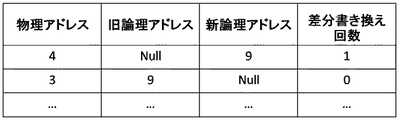
図2に、物理アドレスと論理アドレスの対応、およびそれぞれの物理アドレスに対する書き換え回数についてのテーブルを示す。NAND型フラッシュメモリ上の管理情報は、メモリシステム1の起動時に揮発性メモリ5上に展開される。メモリコントローラ7は、通常動作時において、揮発性メモリ5上に展開された管理情報に基づき、第1の不揮発性メモリ4へのデータ書き込み、及び第1の不揮発性メモリ4からのデータ読み出しを実行する。また、データ書き込みに伴い、揮発性メモリ5に記憶された管理情報は更新されるが、第1の不揮発性メモリ4に記憶された管理情報は必ずしもは最新状態のものに更新されない。その結果として、第1の不揮発性メモリ4に、最新状態でない管理情報(以下、旧管理情報という)が記憶されている状況が生じる。 FIG. 2 shows a table of correspondence between physical addresses and logical addresses, and the number of rewrites for each physical address. The management information on the NAND flash memory is expanded on the volatile memory 5 when the memory system 1 is activated. The memory controller 7 executes data writing to the first nonvolatile memory 4 and data reading from the first nonvolatile memory 4 based on the management information developed on the volatile memory 5 during normal operation. To do. Further, the management information stored in the volatile memory 5 is updated as data is written, but the management information stored in the first nonvolatile memory 4 is not necessarily updated to the latest state. As a result, there arises a situation in which management information that is not in the latest state (hereinafter referred to as old management information) is stored in the first nonvolatile memory 4.

揮発性メモリ5は、メモリコントローラ7によって第1の不揮発性メモリ4に書き込み又は読み出しをする際に、一時的にデータが格納されるキャッシュメモリであり、また最新状態の管理情報(以下、最新管理情報という)を記憶する役割を持つ。メモリコントローラ7は、第1の不揮発性メモリ4へのデータ書き込みに伴い、揮発性メモリ5に記憶された管理情報を更新する。なお、揮発性メモリ5は、ホスト装置3における最新のユーザデータ8を記憶するものでもよい。 The volatile memory 5 is a cache memory in which data is temporarily stored when data is written to or read from the first nonvolatile memory 4 by the memory controller 7, and management information in the latest state (hereinafter referred to as latest management). Information). The memory controller 7 updates the management information stored in the volatile memory 5 as data is written to the first nonvolatile memory 4. The volatile memory 5 may store the latest user data 8 in the host device 3.

第2の不揮発性メモリ6は、揮発性メモリ5上で管理情報が更新されるとき、その管理情報の更新データ、すなわち揮発性メモリ5に記憶する最新管理情報9と旧管理情報10との差分データ(以下、管理情報差分データという)を記憶するものである。メモリコントローラ7は、第1の不揮発性メモリ4へのデータ書き込みに伴い、揮発性メモリ5に記憶された管理情報を更新する際に、管理情報差分データ11を第2の不揮発性メモリ6に記憶する。図3における管理情報差分テーブルが示すように、管理情報差分データ11は、NAND型フラッシュメモリ上の物理アドレス、旧論理アドレスおよび新論理アドレス、物理アドレスに対する書き換え回数についてのテーブルを含むものである。旧論理アドレスとは、揮発性メモリ5に記憶される管理情報の更新前における論理アドレスをいい、新論理アドレスとは、管理情報の更新後における論理アドレスをいう。 When the management information is updated on the volatile memory 5, the second nonvolatile memory 6 updates the management information, that is, the difference between the latest management information 9 stored in the volatile memory 5 and the old management information 10. Data (hereinafter referred to as management information difference data) is stored. The memory controller 7 stores the management information difference data 11 in the second nonvolatile memory 6 when updating the management information stored in the volatile memory 5 in accordance with the data writing to the first nonvolatile memory 4. To do. As shown in the management information difference table in FIG. 3, the management information difference data 11 includes a table on the physical address, the old logical address and the new logical address, and the number of rewrites to the physical address on the NAND flash memory. The old logical address is a logical address before the management information stored in the volatile memory 5 is updated, and the new logical address is a logical address after the management information is updated.

ここで第2の不揮発性メモリ6の記憶容量は、例えば、第1の不揮発性メモリ4よりも小さい。あるいは、第2の不揮発性メモリ6の記憶容量は、揮発性メモリ5よりも小さい。また、第2の不揮発性メモリ6は、例えば、第1の不揮発性メモリ4よりもレイテンシが小さく、更に、ランダムアクセスが可能である。また、第2の不揮発性メモリ6は、例えば、第1の不揮発性メモリ4よりも書き換え可能回数が多い。また、第2の不揮発性メモリ6は、例えば、第1の不揮発性メモリ4よりも信頼性が高い。   Here, the storage capacity of the second nonvolatile memory 6 is smaller than that of the first nonvolatile memory 4, for example. Alternatively, the storage capacity of the second nonvolatile memory 6 is smaller than that of the volatile memory 5. In addition, the second nonvolatile memory 6 has, for example, a latency lower than that of the first nonvolatile memory 4 and can be randomly accessed. In addition, the second nonvolatile memory 6 can be rewritten more times than the first nonvolatile memory 4, for example. The second nonvolatile memory 6 is more reliable than the first nonvolatile memory 4, for example.

かかるメモリを用いることにより、メモリシステム1の処理速度および信頼性を損なうことなく、異常な電源断に対応することができる。第2の不揮発性メモリ6には、例えばFeRAM(Ferroelectric Random Access Memory)又はMRAM(Magnetoresistive Random Access Memory)が用いられる。本実施形態に係るメモリシステム1では、第1の不揮発性メモリ4として用いられるNAND型フラッシュメモリに、更新回数の多い管理情報差分データ11を記憶しないことにより、メモリシステム1の信頼性を確保している。   By using such a memory, it is possible to cope with an abnormal power cut without impairing the processing speed and reliability of the memory system 1. For the second nonvolatile memory 6, for example, FeRAM (Ferroelectric Random Access Memory) or MRAM (Magnetoresistive Random Access Memory) is used. In the memory system 1 according to the present embodiment, the reliability of the memory system 1 is ensured by not storing the management information difference data 11 with a large number of updates in the NAND flash memory used as the first nonvolatile memory 4. ing.

メモリコントローラ7は、第1の不揮発性メモリ4、揮発性メモリ5および第2の不揮発性メモリ6と、インターフェース2を介して接続されたホスト装置3とのデータの送受信について制御するものである。また、メモリコントローラ7は、管理情報の更新、管理情報差分データの記憶、異常電源断からの復元など、後述するメモリシステム1の各動作を制御する。   The memory controller 7 controls transmission / reception of data between the first nonvolatile memory 4, the volatile memory 5 and the second nonvolatile memory 6 and the host device 3 connected via the interface 2. Further, the memory controller 7 controls each operation of the memory system 1 to be described later, such as management information update, storage of management information difference data, and restoration from abnormal power interruption.

以下、メモリシステム1の動作について図面を参照しながら説明する。 Hereinafter, the operation of the memory system 1 will be described with reference to the drawings.

(管理情報差分データの保存形式)
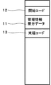
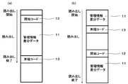
図4は、第2の不揮発性メモリ6上における管理情報差分データ11の保存形式を示す図である。有効な管理情報差分データ11の領域を開始コード12および末端コード13によって識別可能にする。開始コード12および末端コード13は管理情報差分データ11および非書き込み領域のパターンと区別可能なように構成する。例えば、冗長ビットを1bit設けることによって開始コード12および末端コード13を識別することができる。
(Storage format of management information difference data)
FIG. 4 is a diagram showing a storage format of the management information difference data 11 on the second nonvolatile memory 6. The area of the effective management information difference data 11 can be identified by the start code 12 and the end code 13. The start code 12 and the end code 13 are configured to be distinguishable from the management information difference data 11 and the pattern of the non-write area. For example, the start code 12 and the end code 13 can be identified by providing 1 bit of redundant bits.

特定のアドレスに対して管理情報差分データ11の書き込みが集中することを防ぐため、本実施形態においては、特定の固定領域に管理情報差分データ11のアドレスを書き込まずに、第2の不揮発性メモリ6のアドレス空間全体を循環的に使用する方式を採る。かかる方式の場合、管理情報差分データ11を読み出すときはアドレス空間の先端から末端コード13までを順に読み出すため、サーチに時間がかかるが、管理情報差分データ11を読み出す場合は異常電源断後の再起動時のみであり、読み出しの遅さによってメモリシステム1の性能が劣化することはない。 In order to prevent the writing of the management
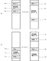
 information difference data 11 from being concentrated on a specific address, in the present embodiment, the second nonvolatile memory is used without writing the address of the management information difference data 11 in a specific fixed area. A method of cyclically using the entire address space of 6 is adopted. In the case of this method, when the management information difference data 11 is read, it takes time to search from the leading end of the address space to the end code 13, so it takes a long time to search. This is only at the time of startup, and the performance of the memory system 1 does not deteriorate due to the delay of reading.

(管理情報差分データの追記方法)
図5を用いて、管理情報差分データ11の追記方法について説明する。図5(a)に、第2の不揮発性メモリ6上に管理情報差分データ11が書き込まれているアドレス空間を示す。かかる状況において、追記される管理情報差分データ11を末端コード13から上書きする。その後、管理情報差分データ11が全て書き込まれた後、かかるデータの直後のアドレスに新たに末端コード13が書き込まれる。この場合、追加されるデータは管理情報差分データ11および新たな末端コード13のみであるため、第2の不揮発性メモリ6への追記を高速に行うことができる。なお、管理情報差分データ11が書き込まれていない状態においても同様の方法で追記することができる。
(Additional method of management information difference data)
A method for adding the management information difference data 11 will be described with reference to FIG. FIG. 5A shows an address space in which the management information difference data 11 is written on the second nonvolatile memory 6. In such a situation, the management information difference data 11 to be added is overwritten from the end code 13. Thereafter, after all the management information difference data 11 is written, a terminal code 13 is newly written at an address immediately after the data. In this case, since the added data is only the management information difference data 11 and the new end code 13, additional writing to the second nonvolatile memory 6 can be performed at high speed. Even in a state where the management information difference data 11 is not written, it can be additionally written by the same method.

図5(b)のように、管理情報差分データ11を追記する際に、管理情報差分データ11の末端がアドレスの終端を超過する場合には、超過分のデータはアドレス空間の先端から順に書き込み、そのデータの直後のアドレスに末端コード13を書き込む。この場合、末端コード13は、開始コード12よりも前のアドレスに書き込まれていることになる。   As shown in FIG. 5B, when the management
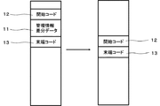
 information difference data 11 is additionally written, if the end of the management information difference data 11 exceeds the end of the address, the excess data is written in order from the top of the address space. The end code 13 is written at the address immediately after the data. In this case, the end code 13 is written at an address before the start code 12.

(管理情報差分データの消去方法)
図6を用いて、管理情報差分データ11の消去方法について説明する。この消去方法は、例えば、メモリシステム1の正常電源断により第1の不揮発性メモリ4上の管理情報が最新のものに更新され、第2の不揮発性メモリ6上の管理情報差分データ11が不要になる場合に用いられる。図6に第2の不揮発性メモリ6上に管理情報差分データ11が書き込まれているアドレス空間を示す。この状態において、開始コード12に無効なデータ、例えば全て0からなるデータにより上書きし、末端コード13には、新たに開始コード12を上書きし、この新たな開始コード12の直後のアドレスに末端コード13を書き込む。この状態では、開始コード12と末端コード13の間には、管理情報差分データ11が書き込まれていない。これにより、第2の不揮発性メモリ6を読みだしたとき、管理情報差分データ11が存在しないものと認識される。この消去方法は、開始コード12および末端コード13への上書きと、新たな末端コード13の書き込みにより行われるため、差分管理情報データの消去を高速に行うことができる。
(Management information difference data deletion method)
A method for deleting the management information difference data 11 will be described with reference to FIG. In this erasing method, for example, the management information on the first nonvolatile memory 4 is updated to the latest by the normal power-off of the memory system 1, and the management information difference data 11 on the second nonvolatile memory 6 is unnecessary. Used when FIG. 6 shows an address space in which the management information difference data 11 is written on the second nonvolatile memory 6. In this state, the start code 12 is overwritten with invalid data, for example, data consisting of all zeros, the end code 13 is newly overwritten with the start code 12, and the end code is added to the address immediately after the new start code 12. 13 is written. In this state, the management information difference data 11 is not written between the start code 12 and the end code 13. Thereby, when the second nonvolatile memory 6 is read, it is recognized that the management information difference data 11 does not exist. Since this erasing method is performed by overwriting the start code 12 and the end code 13 and writing a new end code 13, the difference management information data can be erased at high speed.

(管理情報差分データの書き換え方法)
図7を用いて、管理情報差分データ11の書き換え方法について説明する。この更新方法は、メモリシステム1の正常電源断により第1の不揮発性メモリ4上の管理情報が最新のものに更新され、第2の不揮発性メモリ6上の管理情報差分データ11が消去されていない状態で新たに差分データを書き込む場合に用いられる。図7に第2の不揮発性メモリ6上に管理情報差分データ11が書き込まれているアドレス空間を示す。この状態において、開始コード12には、無効なデータ、例えば全て0からなるデータにより上書きし、末端コード13には、新たに開始コード12を上書きし、開始コード12の直後のアドレスから管理情報差分データ11を書き込み、その後管理情報差分データ11の末端に、末端コード13を書き込む。この書き換え方法によれば、開始コード12および末端コード13への上書きと管理情報差分データ11の書き込みと、新たな末端コード13の書き込みにより行われるため、差分管理情報データ11の書き換えを高速に行うことができる。
(Management information difference data rewriting method)
A method for rewriting the management information difference data 11 will be described with reference to FIG. In this updating method, the management information on the first nonvolatile memory 4 is updated to the latest by the normal power-off of the memory system 1, and the management information difference data 11 on the second nonvolatile memory 6 is erased. This is used when differential data is newly written in the absence of the data. FIG. 7 shows an address space in which the management information difference data 11 is written on the second nonvolatile memory 6. In this state, the start code 12 is overwritten with invalid data, for example, data consisting of all 0s, the end code 13 is newly overwritten with the start code 12, and the management information difference from the address immediately after the start code 12 is overwritten. The data 11 is written, and then the end code 13 is written at the end of the management information difference data 11. According to this rewriting method, it is performed by overwriting the start code 12 and the end code 13, writing the management information difference data 11, and writing a new end code 13, so that the difference management information data 11 is rewritten at high speed. be able to.

(管理情報差分データの読み出し方法)
図8に第1の実施形態に係る第2の不揮発性メモリにおいて管理情報差分データ11の読み出し方法を示すフローチャートを示し、図9に開始コード12が末端コード13より前にある場合と後にある場合におけるアドレス空間を示す。以下、図8および図9を用いて、管理情報差分データ11の読み出し方法を説明する。
(How to read management information difference data)
FIG. 8 shows a flowchart showing a method for reading the management information difference data 11 in the second nonvolatile memory according to the first embodiment, and FIG. 9 shows a case where the start code 12 is before and after the end code 13. Indicates the address space at. Hereinafter, a method for reading the management information difference data 11 will be described with reference to FIGS. 8 and 9.

まず、メモリコントローラ7は、第2の不揮発性メモリ6のアドレス空間の先端からアドレスをインクリメントし、読み出し動作を行う(S101)。その後、メモリコントローラ7は、読み出したデータが開始コード12又は末端コード13か否かを判定する(S102)。   First, the memory controller 7 increments the address from the tip of the address space of the second nonvolatile memory 6 and performs a read operation (S101). Thereafter, the memory controller 7 determines whether the read data is the start code 12 or the end code 13 (S102).

読み出したデータが開始コード12又は末端コード13ではない場合、メモリコントローラ7は、再びアドレスをインクリメントし、読み出し動作を行う(S101)。一方、読み出したデータが開始コード12又は末端コード13である場合、メモリコントローラ7は、読み出したコードが開始コード12であるか否かを判定する(S103)。   If the read data is not the start code 12 or the end code 13, the memory controller 7 increments the address again and performs a read operation (S101). On the other hand, when the read data is the start code 12 or the end code 13, the memory controller 7 determines whether or not the read code is the start code 12 (S103).

読み出したコードが開始コード12である場合、メモリコントローラ7は、アドレスをインクリメントし、読み出し動作を行う(S104)。その後、メモリコントローラ7は、末端コード13を読み出したか否かを判定する(S105)。末端コード13を読み出さない場合、メモリコントローラ7は、再びアドレスをインクリメントし、読み出し動作を行う(S104)。末端コード13を読み出した場合、メモリコントローラ7は、管理情報差分データ11を、開始コード12直後のアドレスから末端コード13直前のアドレスまでのデータとして読み込む(S106)。 If the read code is the start code 12, the memory controller 7 increments the address and performs a read operation (S104). Thereafter, the memory controller 7 determines whether or not the end code 13 has been read (S105). If the terminal code 13 is not read, the memory controller 7 increments the address again and performs a read operation (S104). When the terminal code 13 is read, the memory controller 7 reads the management information difference data 11 as data from the address immediately after the start code 12 to the address immediately before the terminal code 13 (S106).

読み出したコードが開始コード12ではない場合、即ち、末端コード13である場合、メモリコントローラ7は、アドレスをインクリメントし、読み出し動作を行う(S107)。その後、メモリコントローラ7は、アドレス空間の末端まで読み出したか否かを判定する(S108)。アドレス空間の末端まで読み出していない場合、メモリコントローラ7は、再びアドレスをインクリメントし、読み出し動作を行う(S107)。 If the read code is not the start code 12, that is, if it is the end code 13, the memory controller 7 increments the address and performs a read operation (S107). Thereafter, the memory controller 7 determines whether or not the end of the address space has been read (S108). If the end of the address space has not been read, the memory controller 7 increments the address again and performs a read operation (S107).

アドレス空間の末端まで読みだした場合、メモリコントローラ7は、管理情報差分データ11を、開始コード12直後のアドレスからアドレス空間の末端までのデータ、およびアドレス空間の先端から末端コード13直前のアドレスまでのデータとして読み込む(S109)。   When reading to the end of the address space, the memory controller 7 reads the management information difference data 11 from the address immediately after the start code 12 to the end of the address space, and from the top of the address space to the address immediately before the end code 13. (S109).

図9(a)のように、開始コード12が末端コード13より前にある場合は、アドレス空間の先端から読み出しを開始し、末端コード13において読み出しを終了する。このとき、管理情報差分データ11は、開始コード12直後のアドレスから末端コード13直前のアドレスまでのデータとして読み込まれる。 As shown in FIG. 9A, when the start code 12 is before the end code 13, reading is started from the leading end of the address space, and reading is ended at the end code 13. At this time, the management information difference data 11 is read as data from the address immediately after the start code 12 to the address immediately before the end code 13.

図9(b)のように、開始コード12が末端コード13より後にある場合は、アドレス空間の先端から読み出しを開始し、アドレス空間末端において読み出しを終了する。このとき、管理情報差分データ11は、開始コード12直後のアドレスからアドレス空間の末端までのデータ、およびアドレス空間の先端から末端コード13直前のアドレスまでのデータとして読み込まれる。 As shown in FIG. 9B, when the start code 12 is after the end code 13, reading is started from the leading end of the address space, and reading is ended at the end of the address space. At this time, the management information difference data 11 is read as data from the address immediately after the start code 12 to the end of the address space, and data from the top of the address space to the address immediately before the end code 13.

(第2の不揮発性メモリ6の記憶領域が全て埋まった場合)
第2の不揮発性メモリ6の記憶領域が管理情報差分データ11により全て埋まった場合には、以下の動作を行う。まず揮発性メモリ5上の最新管理情報9を第1の不揮発性メモリ4に書き込み、第1の不揮発性メモリ4上の管理情報を最新のものにする。その後、第2の不揮発性メモリ6上の管理情報差分データ11を消去する。これにより、管理情報差分データ11が、第2の不揮発性メモリ6の記憶領域を確保することができる。なお、第2の不揮発性メモリ6の記憶領域が全て埋まった場合において、第2の不揮発性メモリ6に記憶できない管理情報差分データ11を第1の不揮発性メモリ4に追記してもよい。
(When the storage area of the second nonvolatile memory 6 is completely filled)
When the storage area of the second nonvolatile memory 6 is completely filled with the management information difference data 11, the following operation is performed. First, the latest management information 9 on the volatile memory 5 is written into the first nonvolatile memory 4 to update the management information on the first nonvolatile memory 4 to the latest. Thereafter, the management information difference data 11 on the second nonvolatile memory 6 is erased. As a result, the management information difference data 11 can secure the storage area of the second nonvolatile memory 6. Note that management information difference data 11 that cannot be stored in the second nonvolatile memory 6 may be additionally written to the first nonvolatile memory 4 when the entire storage area of the second nonvolatile memory 6 is filled.

以下、正常な電源断が行われた場合および異常な電源断が発生した場合について説明する。   Hereinafter, a case where a normal power-off and an abnormal power-off occur will be described.

(正常な電源断が行われる場合)
正常な電源断が行われる場合のメモリシステム1の動作について説明する。正常に電源断を行う際に、揮発性メモリ5上の最新管理情報9を第1の不揮発性メモリ4に書き込み、第1の不揮発性メモリ4上の管理情報を最新のものにする。その後、第2の不揮発性メモリ6上の管理情報差分データ11を消去する。これにより、第2の不揮発性メモリ6の記憶領域に、管理情報差分データ11が全て埋まることを防止することができる。次回のメモリシステム1の起動時には、第1の不揮発性メモリ4に記憶された最新の管理情報を揮発性メモリ5に展開する。
(When normal power is cut off)
An operation of the memory system 1 when a normal power cut is performed will be described. When the power is normally cut off, the latest management information 9 on the volatile memory 5 is written into the first nonvolatile memory 4 to update the management information on the first nonvolatile memory 4 to the latest. Thereafter, the management information difference data 11 on the second nonvolatile memory 6 is erased. Thereby, it is possible to prevent the management information difference data 11 from being completely buried in the storage area of the second nonvolatile memory 6. When the memory system 1 is activated next time, the latest management information stored in the first nonvolatile memory 4 is expanded in the volatile memory 5.

なお、正常に電源断を行う際に、必ずしも揮発性メモリ5上の最新管理情報9を第1の不揮発性メモリ4に書き込まなくても良い場合も想定され得る。例えば、管理情報差分データ11のサイズが小さく、第2の不揮発性メモリ6の記憶領域の容量に余裕がある場合や、起動時に管理情報差分データ11によって最新の管理情報を復元するために十分な時間が仕様上規定されている場合等である。 Note that it may be assumed that the latest management information 9 on the volatile memory 5 does not necessarily have to be written in the first nonvolatile memory 4 when the power is normally shut off. For example, when the size of the management information difference data 11 is small and the storage area of the second nonvolatile memory 6 has a sufficient capacity, it is sufficient to restore the latest management information by the management information difference data 11 at the time of startup. This is the case when the time is specified in the specification.

(異常な電源断が発生した場合)
上述の正常な電源断が行われず、異常な電源断が発生した場合において、メモリシステム1におけるデータ復元の動作について説明する。異常な電源断が発生した場合、揮発性メモリ5上の最新管理情報9のデータが失われるため、次回のメモリシステム1の起動時に管理情報のデータ復元が行われる。
(If an abnormal power failure occurs)
A data restoration operation in the memory system 1 when the above-described normal power-off is not performed and an abnormal power-off occurs will be described. When an abnormal power interruption occurs, the data of the latest management information 9 on the volatile memory 5 is lost, so that the management information data is restored at the next startup of the memory system 1.

まず、第1の不揮発性メモリ4上の旧管理情報10を揮発性メモリ5に読み込む。その後、第2の不揮発性メモリ6上の管理情報差分データ11に基づいて、揮発性メモリ5上の旧管理情報10を最新管理情報9に復元する。 First, the old management information 10 on the first nonvolatile memory 4 is read into the volatile memory 5. Thereafter, based on the management information difference data 11 on the second nonvolatile memory 6, the old management information 10 on the volatile memory 5 is restored to the latest management information 9.

なお、上記動作後に、揮発性メモリ5上の更新された最新管理情報9を第1の不揮発性メモリ4に書き込みをしてもよい。異常な電源断後の再起動の際には、比較的長い起動時間が許容されるため、一度、最新管理情報9を第1の不揮発性メモリ4に書き込む事で、メモリシステム1の動作を安定させる事ができる。また、その後、第2の不揮発性メモリ6上の管理情報差分データ11を消去してもよい。これにより、第2の不揮発性メモリ6の記憶領域に、管理情報差分データ11が全て埋まることを防止することができる。 Note that the updated latest management information 9 on the volatile memory 5 may be written to the first nonvolatile memory 4 after the above operation. When restarting after an abnormal power failure, a relatively long startup time is allowed. Therefore, once the latest management information 9 is written to the first nonvolatile memory 4, the operation of the memory system 1 is stabilized. You can make it. Thereafter, the management information difference data 11 on the second nonvolatile memory 6 may be erased. Thereby, it is possible to prevent the management information difference data 11 from being completely buried in the storage area of the second nonvolatile memory 6.

以上のように、本発明の第1の実施形態によれば、メモリシステム1において、管理情報差分データ11を記憶するために、第2の不揮発性メモリ6として小容量の高速不揮発性メモリを使用している。第2の不揮発性メモリ6にはデータ量が小さい差分データが記憶されるため、第2の不揮発性メモリ6には、コストが低い小容量の高速不揮発性メモリを用いることができ、高速に動作することができる。 As described above, according to the first embodiment of the present invention, a small-capacity high-speed nonvolatile memory is used as the second nonvolatile memory 6 in the memory system 1 to store the management information difference data 11. is doing. Since differential data with a small amount of data is stored in the second non-volatile memory 6, a small-capacity high-speed non-volatile memory with low cost can be used for the second non-volatile memory 6 and it operates at high speed. can do.

さらに、第1の実施形態によれば、第2の不揮発性メモリ6に管理情報差分データ11を記憶している。したがって、異常電源断が発生しても、次回の電源起動時において、異常電源断前の最新の管理情報に復元することができる。   Furthermore, according to the first embodiment, the management information difference data 11 is stored in the second nonvolatile memory 6. Therefore, even when an abnormal power interruption occurs, the latest management information before the abnormal power interruption can be restored at the next power activation.

(第2の実施形態)
本発明の第2の実施形態によるメモリシステム1について図10を用いて説明する。この第2の実施形態の構成について第1の実施形態のメモリシステム1の構成と同一部分は同一符号で示し、その詳細な説明を省略する。この第2の実施形態が、第1の実施形態と異なる点は、図1の第2の不揮発性メモリ6がメモリコントローラ7とは独立して設けられていたものに代えて、メモリコントローラ7のチップ内部に第2の不揮発性メモリ6を組み込み型メモリとして実装する点である。例えば、メモリコントローラ7のチップにFeRAM又はMRAM等の高速の不揮発性メモリを組み込むことができる。
(Second Embodiment)
A memory system 1 according to a second embodiment of the present invention will be described with reference to FIG. In the configuration of the second embodiment, the same parts as those of the memory system 1 of the first embodiment are denoted by the same reference numerals, and detailed description thereof is omitted. The second embodiment is different from the first embodiment in that the second nonvolatile memory 6 in FIG. 1 is replaced with a memory controller 7 provided independently of the memory controller 7. The second nonvolatile memory 6 is mounted as an embedded memory inside the chip. For example, a high-speed nonvolatile memory such as FeRAM or MRAM can be incorporated in the chip of the memory controller 7.

第2の実施形態に係るメモリシステム1においても、第2の不揮発性メモリ6に管理情報差分データ11を記憶することにより、第1の実施形態に係るメモリシステム1の同様の保存方式において、管理情報差分データ11の追記、消去、書き換え、読み出しを行うことができる。   Also in the memory system 1 according to the second embodiment, the management information difference data 11 is stored in the second nonvolatile memory 6, so that the same storage method as that of the memory system 1 according to the first embodiment can be used. Additional writing, erasing, rewriting and reading of the information difference data 11 can be performed.

以上のように、本発明の第2の実施形態によれば、メモリシステム1において、管理情報差分データ11を記憶するために、第2の不揮発性メモリ6として小容量の高速不揮発性メモリを使用している。データ負担が小さい差分のデータを記憶するため、コストが低い高速の不揮発性メモリを用いることができ、さらに高速に動作することができる。   As described above, according to the second embodiment of the present invention, a small-capacity high-speed nonvolatile memory is used as the second nonvolatile memory 6 in the memory system 1 to store the management information difference data 11. is doing. Since differential data with a small data burden is stored, a high-speed nonvolatile memory with low cost can be used, and operation can be performed at higher speed.

さらに、第2の実施形態によれば、第2の不揮発性メモリ6に管理情報差分データ11を記憶している。したがって、異常電源断が発生しても、次回の電源起動時において、異常電源断前の最新の管理情報に復元することができる。   Furthermore, according to the second embodiment, the management information difference data 11 is stored in the second nonvolatile memory 6. Therefore, even when an abnormal power interruption occurs, the latest management information before the abnormal power interruption can be restored at the next power activation.

また、第2の実施形態においては、メモリコントローラ7内に管理情報差分データ11を記憶する第2の不揮発性メモリ6を組み込んでいる。これにより、第1の実施形態に係るメモリシステム1に比べて小面積のメモリシステム1を作成することができる。さらに、第2の不揮発性メモリ6とメモリコントローラ7を結ぶ配線が短くなることにより、ノイズなく、高速に動作するメモリシステム1を提供することができる。
なお、本発明は、上述の実施形態にのみ限定されるものではなく、本発明の要旨を逸脱しない範囲内において種々変更を加え得ることは勿論である。
In the second embodiment, the second nonvolatile memory 6 for storing the management information difference data 11 is incorporated in the memory controller 7. Thereby, the memory system 1 having a smaller area than the memory system 1 according to the first embodiment can be created. Furthermore, since the wiring connecting the second nonvolatile memory 6 and the memory controller 7 is shortened, the memory system 1 that operates at high speed without noise can be provided.
It should be noted that the present invention is not limited to the above-described embodiment, and various modifications can be made without departing from the scope of the present invention.

本発明のいくつかの実施形態を説明したが、これらの実施形態は、例として提示したものであり、発明の範囲を限定することは意図していない。これらの実施形態は、その他のさまざまな形態で実施されることが可能であり、発明の要旨を逸脱しない範囲で、種々の省略、置き換え、変更を行うことができる。これらの実施形態やその変形は、発明の範囲や要旨に含まれると同様に、特許請求の範囲に記載された発明とその均等の範囲に含まれるものである。   Although several embodiments of the present invention have been described, these embodiments are presented by way of example and are not intended to limit the scope of the invention. These embodiments can be implemented in various other forms, and various omissions, replacements, and changes can be made without departing from the spirit of the invention. These embodiments and modifications thereof are included in the invention described in the claims and equivalents thereof as well as included in the scope and gist of the invention.

1…メモリシステム
2…インターフェース
3…ホスト装置
4…第1の不揮発性メモリ
5…揮発性メモリ
6…第2の揮発性メモリ
7…メモリコントローラ
8…ユーザデータ
9…最新管理情報
10…旧管理情報
11…管理情報差分データ
12…開始コード
13…末端コード
DESCRIPTION OF SYMBOLS 1 ... Memory system 2 ... Interface 3 ... Host apparatus 4 ... 1st non-volatile memory 5 ... Volatile memory 6 ... 2nd volatile memory 7 ... Memory controller 8 ... User data 9 ... Latest management information 10 ... Old management information 11 ... Management information difference data 12 ... Start code 13 ... End code

Claims (13)

揮発性メモリと、
前記揮発性半導体メモリに接続された第1の不揮発性メモリと、
前記揮発性半導体メモリに接続された第2の不揮発性メモリと、
前記揮発性メモリに最新管理情報を記憶し、前記第1の不揮発性メモリに旧管理情報を記憶し、および前記第2の不揮発性メモリに前記最新管理情報と前記旧管理情報の差分データを記憶するメモリコントローラと、
を備えたメモリシステム。
Volatile memory,
A first non-volatile memory connected to the volatile semiconductor memory;
A second nonvolatile memory connected to the volatile semiconductor memory;
The latest management information is stored in the volatile memory, the old management information is stored in the first nonvolatile memory, and the difference data between the latest management information and the old management information is stored in the second nonvolatile memory. A memory controller to
With a memory system.
前記第2の不揮発性メモリは、前記第1の不揮発性メモリよりレイテンシが小さく、かつ前記揮発性メモリより小容量のものであることを特徴とする請求項1に記載のメモリシステム。   The memory system according to claim 1, wherein the second nonvolatile memory has a latency smaller than that of the first nonvolatile memory and has a smaller capacity than the volatile memory. 前記第2の不揮発性メモリは、前記第1の不揮発性メモリより書き換え可能回数が多いものであることを特徴とする請求項1又は請求項2に記載のメモリシステム。 3. The memory system according to claim 1, wherein the second nonvolatile memory has a larger number of rewrites than the first nonvolatile memory. 4. 前記第2の不揮発性メモリが、前記メモリコントローラ内に組み込まれたことを特徴とする請求項1乃至請求項3の何れか1項に記載のメモリシステム。   4. The memory system according to claim 1, wherein the second nonvolatile memory is incorporated in the memory controller. 5. 前記メモリコントローラは、異常な電源断が発生した場合に、前記旧管理情報と、前記差分データに基づき、前記揮発性メモリ上に前記最新管理情報を復元することを特徴とする請求項1乃至請求項4の何れか1項に記載のメモリシステム。   The memory controller restores the latest management information on the volatile memory based on the old management information and the difference data when an abnormal power failure occurs. Item 5. The memory system according to any one of Items 4 to 5. 前記メモリコントローラは、正常な電源断を行う場合に、前記最新管理情報を前記第1の不揮発性メモリに書き込み、前記差分データを消去することを特徴とする請求項1乃至請求項5の何れか1項に記載のメモリシステム。   6. The memory controller according to claim 1, wherein the memory controller writes the latest management information in the first nonvolatile memory and erases the difference data when performing a normal power shutdown. 2. The memory system according to item 1. 前記メモリコントローラは、前記第2の不揮発性メモリにおいて、前記差分データの直前のアドレスに開始コードを記憶し、前記差分データの直後のアドレスに末端コードを記憶することを特徴とする請求項1乃至請求項6の何れか1項に記載のメモリシステム。   The memory controller stores a start code at an address immediately before the differential data and stores a terminal code at an address immediately after the differential data in the second nonvolatile memory. The memory system according to claim 6. 前記メモリコントローラは、前記差分データを追記する場合に、前記末端コードのアドレスから前記差分データを記憶し、前記差分データの直後のアドレスに新たな末端コードを記憶することを特徴とする請求項7に記載のメモリシステム。   The said memory controller memorize | stores the said difference data from the address of the said end code, and memorize | stores a new end code in the address immediately after the said difference data, when adding the said difference data. The memory system described in. 前記メモリコントローラは、前記差分データを消去する場合に、前記末端コードのアドレスに新たな開始コードを記憶し、前記新たな開始コードの直後のアドレスに新たな末端コードを記憶することを特徴とする請求項7又は請求項8に記載のメモリシステム。   When erasing the difference data, the memory controller stores a new start code at the address of the end code and stores a new end code at an address immediately after the new start code. The memory system according to claim 7 or 8. 前記メモリコントローラは、前記差分データを書き換える場合に、前記末端コードのアドレスに新たな開始コードを記憶し、前記新たな開始コードの直後のアドレスから前記差分データを記憶し、かつ前記差分データの直後のアドレスに新たな末端コードを記憶することを特徴とする請求項7乃至請求項9の何れか1項に記載のメモリシステム。   When rewriting the difference data, the memory controller stores a new start code at the address of the end code, stores the difference data from an address immediately after the new start code, and immediately after the difference data. 10. The memory system according to claim 7, wherein a new end code is stored at the address. 前記メモリコントローラは、前記差分データを読み出す場合において、前記第2の不揮発性メモリの先端アドレスから順にアドレスをインクリメントして読み出しを実行し、前記末端コードよりも先に前記開始コードを読み出した場合に、前記開始コードの直後のアドレスから前記末端コードの直前のアドレスまでのデータを前記差分データとして読み込むことを特徴とする請求項7乃至請求項10の何れか1項に記載のメモリシステム。   When reading the difference data, the memory controller increments the address in order from the leading end address of the second nonvolatile memory, executes the reading, and reads the start code before the end code. 11. The memory system according to claim 7, wherein data from an address immediately after the start code to an address immediately before the end code is read as the difference data. 前記メモリコントローラは、前記差分データを読み出す場合において、前記第2の不揮発性メモリの先端アドレスから順にアドレスをインクリメントして読み出しを実行し、前記開始コードよりも先に前記末端コードを読み出した場合に、前記先端アドレスから前記末端コードの直前のアドレスまで、および前記開始コードの直後のアドレスから前記第2の不揮発性メモリの末端アドレスまでのデータを管理情報差分データとして読み込むことを特徴とする請求項7乃至請求項11の何れか1項に記載のメモリシステム。   When reading the difference data, the memory controller increments the address sequentially from the leading end address of the second non-volatile memory, executes the reading, and reads the end code before the start code. The data from the leading address to the address immediately before the end code and from the address immediately after the start code to the end address of the second nonvolatile memory is read as management information difference data. The memory system according to any one of claims 7 to 11. 前記メモリコントローラは、前記第2の不揮発性メモリが前記差分データで埋まった場合に、前記最新管理情報を前記第1の不揮発性メモリに書き込み、かつ前記差分データを消去することを特徴とする請求項7乃至請求項12の何れか1項に記載のメモリシステム。   The memory controller, when the second non-volatile memory is filled with the difference data, writes the latest management information to the first non-volatile memory and erases the difference data. The memory system according to any one of Items 7 to 12.
JP2010255411A 2010-11-15 2010-11-15 Memory system Pending JP2012108627A (en)

Priority Applications (2)

Application Number Priority Date Filing Date Title
JP2010255411A JP2012108627A (en) 2010-11-15 2010-11-15 Memory system
US13/069,963 US20120124275A1 (en) 2010-11-15 2011-03-23 Memory system and data storage method

Applications Claiming Priority (1)

Application Number Priority Date Filing Date Title
JP2010255411A JP2012108627A (en) 2010-11-15 2010-11-15 Memory system

Publications (2)

Publication Number Publication Date
JP2012108627A true JP2012108627A (en) 2012-06-07
JP2012108627A5 JP2012108627A5 (en) 2013-08-01

Family

ID=46048858

Family Applications (1)

Application Number Title Priority Date Filing Date
JP2010255411A Pending JP2012108627A (en) 2010-11-15 2010-11-15 Memory system

Country Status (2)

Country Link
US (1) US20120124275A1 (en)
JP (1) JP2012108627A (en)

Cited By (1)

* Cited by examiner, † Cited by third party
Publication number Priority date Publication date Assignee Title
US9063845B2 (en) 2012-08-29 2015-06-23 Buffalo Memory Co., Ltd. Solid-state drive device

Families Citing this family (2)

* Cited by examiner, † Cited by third party
Publication number Priority date Publication date Assignee Title
US9032264B2 (en) 2013-03-21 2015-05-12 Kabushiki Kaisha Toshiba Test method for nonvolatile memory
EP3644191A4 (en) * 2017-06-20 2021-03-24 Kyocera Document Solutions Inc. Memory system and electronic device

Citations (5)

* Cited by examiner, † Cited by third party
Publication number Priority date Publication date Assignee Title
JPH08328821A (en) * 1995-05-30 1996-12-13 Kokusai Electric Co Ltd Searching method for data reading point
JP2000105694A (en) * 1998-09-28 2000-04-11 Nec Ic Microcomput Syst Ltd Flash memory, microcomputer equipped with flash memory, and method for storing program in flash memory
JP2007156846A (en) * 2005-12-05 2007-06-21 Tdk Corp Memory controller and flash memory system
JP2009009213A (en) * 2007-06-26 2009-01-15 Ricoh Co Ltd Data storage system, program, and data storage method
JP2009211223A (en) * 2008-03-01 2009-09-17 Toshiba Corp Memory system

Family Cites Families (8)

* Cited by examiner, † Cited by third party
Publication number Priority date Publication date Assignee Title
JP3603333B2 (en) * 1994-06-22 2004-12-22 カシオ計算機株式会社 Data processing device
US5568443A (en) * 1995-09-08 1996-10-22 Smithills Multimedia Systems, Inc. Combination dual-port random access memory and multiple first-in-first-out (FIFO) buffer memories
US6732223B1 (en) * 2000-04-03 2004-05-04 Micron Technology, Inc. Method and apparatus for address FIFO for high-bandwidth command/address busses in digital storage system
JP2005115857A (en) * 2003-10-10 2005-04-28 Sony Corp File storage device
US20050251617A1 (en) * 2004-05-07 2005-11-10 Sinclair Alan W Hybrid non-volatile memory system
US8028123B2 (en) * 2008-04-15 2011-09-27 SMART Modular Technologies (AZ) , Inc. Circular wear leveling
US8843691B2 (en) * 2008-06-25 2014-09-23 Stec, Inc. Prioritized erasure of data blocks in a flash storage device
JP5317690B2 (en) * 2008-12-27 2013-10-16 株式会社東芝 Memory system

Patent Citations (5)

* Cited by examiner, † Cited by third party
Publication number Priority date Publication date Assignee Title
JPH08328821A (en) * 1995-05-30 1996-12-13 Kokusai Electric Co Ltd Searching method for data reading point
JP2000105694A (en) * 1998-09-28 2000-04-11 Nec Ic Microcomput Syst Ltd Flash memory, microcomputer equipped with flash memory, and method for storing program in flash memory
JP2007156846A (en) * 2005-12-05 2007-06-21 Tdk Corp Memory controller and flash memory system
JP2009009213A (en) * 2007-06-26 2009-01-15 Ricoh Co Ltd Data storage system, program, and data storage method
JP2009211223A (en) * 2008-03-01 2009-09-17 Toshiba Corp Memory system

Cited By (2)

* Cited by examiner, † Cited by third party
Publication number Priority date Publication date Assignee Title
US9063845B2 (en) 2012-08-29 2015-06-23 Buffalo Memory Co., Ltd. Solid-state drive device
US9632714B2 (en) 2012-08-29 2017-04-25 Buffalo Memory Co., Ltd. Solid-state drive device

Also Published As

Publication number Publication date
US20120124275A1 (en) 2012-05-17

Similar Documents

Publication Publication Date Title
US8862808B2 (en) Control apparatus and control method
US9400744B2 (en) Magnetic random access memory journal for multi-level cell flash memory
JP5317690B2 (en) Memory system
US9026764B2 (en) Memory system performing wear leveling based on deletion request
JP4524309B2 (en) Memory controller for flash memory
JP4871260B2 (en) MEMORY MODULE, MEMORY CONTROLLER, NONVOLATILE STORAGE DEVICE, NONVOLATILE STORAGE SYSTEM, AND MEMORY READ / WRITE METHOD
US20150331624A1 (en) Host-controlled flash translation layer snapshot
JP5990430B2 (en) SSD (solid state drive) device
CN111752487B (en) Data recovery method and device and solid state disk
JP5983019B2 (en) Control device, storage device, and storage control method
US10838629B2 (en) Solid state device with fast boot after ungraceful shutdown
TWI662410B (en) Data storage device and methods for processing data in the data storage device
US20190324859A1 (en) Method and Apparatus for Restoring Data after Power Failure for An Open-Channel Solid State Drive
JP5631938B2 (en) Semiconductor memory device
US9208101B2 (en) Virtual NAND capacity extension in a hybrid drive
KR20120086239A (en) Memory system and operation method thereof
US10152280B2 (en) Storage device and control method
US20170147232A1 (en) Solid state drive and data programming method thereof
JP2013222435A (en) Semiconductor storage device and method of controlling the same
JP5874525B2 (en) Control device, storage device, and storage control method
US8527733B2 (en) Memory system
US10942811B2 (en) Data processing method for solid state drive
JP2012108627A (en) Memory system
JP2006099802A (en) Storage controller, and control method for cache memory
US20190243580A1 (en) Dram-based storage device and associated data processing method

Legal Events

Date Code Title Description
A521 Request for written amendment filed

Free format text: JAPANESE INTERMEDIATE CODE: A523

Effective date: 20130614

A621 Written request for application examination

Free format text: JAPANESE INTERMEDIATE CODE: A621

Effective date: 20130614

A977 Report on retrieval

Free format text: JAPANESE INTERMEDIATE CODE: A971007

Effective date: 20140115

A131 Notification of reasons for refusal

Free format text: JAPANESE INTERMEDIATE CODE: A131

Effective date: 20140214

A02 Decision of refusal

Free format text: JAPANESE INTERMEDIATE CODE: A02

Effective date: 20140704