JP2012105277A - Level shifter, system-on-chip including the same, and multimedia device including the same - Google Patents
Level shifter, system-on-chip including the same, and multimedia device including the same Download PDFInfo
- Publication number
- JP2012105277A JP2012105277A JP2011247518A JP2011247518A JP2012105277A JP 2012105277 A JP2012105277 A JP 2012105277A JP 2011247518 A JP2011247518 A JP 2011247518A JP 2011247518 A JP2011247518 A JP 2011247518A JP 2012105277 A JP2012105277 A JP 2012105277A
- Authority
- JP
- Japan
- Prior art keywords
- voltage
- clock
- control unit
- inverter
- processor
- Prior art date
- Legal status (The legal status is an assumption and is not a legal conclusion. Google has not performed a legal analysis and makes no representation as to the accuracy of the status listed.)
- Pending
Links
Images


Classifications
-
- H—ELECTRICITY
- H03—ELECTRONIC CIRCUITRY
- H03K—PULSE TECHNIQUE
- H03K19/00—Logic circuits, i.e. having at least two inputs acting on one output; Inverting circuits
- H03K19/0175—Coupling arrangements; Interface arrangements
- H03K19/0185—Coupling arrangements; Interface arrangements using field effect transistors only
- H03K19/018507—Interface arrangements
- H03K19/018521—Interface arrangements of complementary type, e.g. CMOS
-
- H—ELECTRICITY
- H03—ELECTRONIC CIRCUITRY
- H03K—PULSE TECHNIQUE
- H03K19/00—Logic circuits, i.e. having at least two inputs acting on one output; Inverting circuits
- H03K19/003—Modifications for increasing the reliability for protection
- H03K19/00315—Modifications for increasing the reliability for protection in field-effect transistor circuits
Landscapes
- Engineering & Computer Science (AREA)
- Computer Hardware Design (AREA)
- Physics & Mathematics (AREA)
- Computing Systems (AREA)
- General Engineering & Computer Science (AREA)
- Mathematical Physics (AREA)
- Logic Circuits (AREA)
- Control Of Indicators Other Than Cathode Ray Tubes (AREA)
Abstract
Description
本発明は電子回路に、より詳細にはレベル変換器、それを含むシステムオンチップ、及びそれを含むマルチメディア装置に関する。 The present invention relates to electronic circuits, and more particularly to level converters, system-on-chip including the same, and multimedia devices including the same.
レベル変換器(level shifter)は第1電圧ドメインの信号を受信し、第1電圧と異なる第2電圧ドメインの信号を出力する素子である。互いに異なる電圧を使用する複数の電圧ドメインの間でレベル変換器が使用される。 The level shifter is an element that receives a first voltage domain signal and outputs a second voltage domain signal different from the first voltage. Level translators are used between multiple voltage domains that use different voltages.
システムオンチップ(SOC、System−On−Chip)は複数のIP(Intellectual Property)及びプロセッサーを含む。プロセッサーはIPより速い動作速度を有する。プロセッサーの動作性能を向上させるために、プロセッサーへ供給されるクロックの電圧レベルはIPへ供給されるクロックの電圧レベルより高く設定され得る。プロセッサーへ供給されるクロックの電圧レベルを上昇させるために、システムオンチップ(SOC)でレベル変換器が使用され得る。 A system on chip (SOC, System-On-Chip) includes a plurality of IPs (Intellectual Properties) and processors. The processor has a faster operating speed than IP. In order to improve the operating performance of the processor, the voltage level of the clock supplied to the processor can be set higher than the voltage level of the clock supplied to the IP. A level converter can be used in the system on chip (SOC) to raise the voltage level of the clock supplied to the processor.
本発明の目的は向上された信頼性を有するレベル変換器、それを含むシステムオンチップ、及びそれを含むマルチメディア装置を提供することにある。 An object of the present invention is to provide a level converter having improved reliability, a system-on-chip including the level converter, and a multimedia device including the level converter.
本発明の実施形態によるレベル変換器は、入力ノードと、前記入力ノードを通じて受信される第1電圧ドメインの入力クロックに応じて第2電圧ドメインの出力クロックを発生するように構成される第1及び第2電圧変換回路と、及び前記出力クロックを出力する出力ノードと、を含み、前記第1及び第2電圧変換回路は同一な構造を有し、前記入力ノード及び出力ノードの間に並列に連結される。 A level converter according to an embodiment of the present invention is configured to generate an output clock of a second voltage domain in response to an input node and an input clock of the first voltage domain received through the input node. A second voltage conversion circuit and an output node for outputting the output clock, wherein the first and second voltage conversion circuits have the same structure and are connected in parallel between the input node and the output node Is done.
実施形態として、前記第1電圧変換回路は前記第2電圧ドメインで動作する少なくとも2つのインバータを含む。 As an embodiment, the first voltage conversion circuit includes at least two inverters operating in the second voltage domain.
実施形態として、前記第2電圧変換回路は前記第1電圧ドメインで動作する少なくとも1つのインバータと前記第2電圧ドメインで動作する少なくとも1つのインバータとを含む。 As an embodiment, the second voltage conversion circuit includes at least one inverter operating in the first voltage domain and at least one inverter operating in the second voltage domain.
実施形態として、前記第2電圧ドメインで動作する少なくとも1つのインバータは前記第1電圧ドメインで動作する少なくとも1つのインバータの出力を受信するように構成される。 As an embodiment, at least one inverter operating in the second voltage domain is configured to receive an output of at least one inverter operating in the first voltage domain.
実施形態として、前記第1電圧変換回路は前記入力ノードの電圧にしたがって第2電圧又は接地電圧を出力する第1インバータ及び前記第1インバータの出力にしたがって前記第2電圧又は接地電圧を出力ノードに出力する第2インバータを含み、前記第2電圧変換回路は前記入力ノードの電圧にしたがって前記第1電圧又は接地電圧を出力する第3インバータ及び前記第3インバータの出力にしたがって前記第2電圧又は接地電圧を前記出力ノードに出力する第4インバータを含む。 As an embodiment, the first voltage converter circuit outputs a second voltage or a ground voltage according to the voltage of the input node, and the second voltage or the ground voltage as an output node according to the output of the first inverter. A second inverter for outputting, wherein the second voltage conversion circuit outputs the first voltage or the ground voltage according to the voltage of the input node, and the second voltage or ground according to the output of the third inverter. A fourth inverter for outputting a voltage to the output node;
実施形態として、前記第1乃至第4インバータはCMOSインバータである。 As an embodiment, the first to fourth inverters are CMOS inverters.
本発明の実施形態によるシステムオンチップは、第1電圧ドメインの第1クロックを発生するように構成される位相ロックループ(PLL)と、前記第1クロックに応じて動作する周辺ブロック、オーディオブロック、ディスプレーブロック、グラフィックブロック、イメージプロセシングブロック、及びコーデックブロックと、前記第1クロックに基づいて、第2電圧ドメインの第2クロックを発生するレベル変換器と、前記第2クロックに応じて動作するプロセッサーを含み、前記レベル変換器は入力ノード及び出力ノードの間に並列に連結され、同一な構造を有する第1及び第2電圧変換回路を含む。 A system-on-chip according to an embodiment of the present invention includes a phase-locked loop (PLL) configured to generate a first clock of a first voltage domain, a peripheral block that operates according to the first clock, an audio block, A display block, a graphics block, an image processing block, and a codec block; a level converter that generates a second clock of a second voltage domain based on the first clock; and a processor that operates according to the second clock. The level converter includes first and second voltage conversion circuits connected in parallel between an input node and an output node and having the same structure.
実施形態として、前記第1電圧変換回路は前記第2電圧ドメインで動作し、直列に連結された第1及び第2インバータを含み、前記第2電圧変換回路は前記第1電圧ドメインで動作する第3インバータ、及び前記第2電圧ドメインで前記第3インバータの出力に応じて動作する第4インバータを含む。 As an embodiment, the first voltage conversion circuit operates in the second voltage domain and includes first and second inverters connected in series, and the second voltage conversion circuit operates in the first voltage domain. And a fourth inverter that operates in response to the output of the third inverter in the second voltage domain.
実施形態として、前記第2電圧ドメインの電圧レベルは前記第1電圧ドメインの電圧レベルより高い。 As an embodiment, the voltage level of the second voltage domain is higher than the voltage level of the first voltage domain.
本発明の実施形態によるマルチメディア装置は、プロセッサーと、前記プロセッサーの動作メモリーと、前記プロセッサーの制御にしたがって外部と通信するように構成されるモデムと、前記プロセッサーの制御にしたがってデータを格納するように構成される格納部と、外部の信号を感知して前記プロセッサーに伝達するように構成される使用者インターフェイス(User Interface)と、前記プロセッサーの制御にしたがって、ディスプレー部を通じて映像を表示するように構成されるディスプレー制御部と、前記プロセッサーの制御にしたがって、スピーカーを通じて音を出力するように構成されるサウンド制御部と、前記プロセッサーの制御にしたがってエンコーディング及びデコーディングを遂行するコーデック部と、発振器の出力にしたがってクロックを発生するように構成されるクロック発生部と、前記クロックに同期される第1電圧ドメインの第1クロックを発生する位相ロックループと、及び前記第1クロックに応じて第2電圧ドメインの第2クロックを発生するように構成されるレベル変換器と、を含み、前記プロセッサーは前記第2クロックに応じて動作し、前記レベル変換器は入力ノード及び出力ノードの間に並列に連結され、同一な構造を有する第1及び第2電圧変換回路を含む。 A multimedia device according to an embodiment of the present invention stores a processor, an operating memory of the processor, a modem configured to communicate with the outside according to the control of the processor, and stores data according to the control of the processor. A storage unit configured to display an image through a display unit according to control of the processor and a user interface configured to detect and transmit an external signal to the processor. A display control unit configured, a sound control unit configured to output sound through a speaker according to the control of the processor, and a codec unit performing encoding and decoding according to the control of the processor A clock generator configured to generate a clock according to an output of the oscillator; a phase-locked loop that generates a first clock of a first voltage domain synchronized with the clock; and a first according to the first clock. A level converter configured to generate a second clock in a two voltage domain, wherein the processor operates in response to the second clock, the level converter being in parallel between an input node and an output node And first and second voltage conversion circuits having the same structure.
実施形態として、前記入力ノードの電圧にしたがって前記第2電圧ドメインの第2電圧又は接地電圧を出力する第1インバータと、前記第1インバータの出力にしたがって前記第2電圧又は接地電圧を出力ノードに出力する第2インバータと、前記入力ノードの電圧にしたがって前記第1電圧ドメインの第1電圧又は接地電圧を出力する第3インバータと、及び前記第3インバータの出力にしたがって前記第2電圧又は接地電圧を前記出力ノードに出力する第4インバータを含む。 As an embodiment, a first inverter that outputs the second voltage or the ground voltage of the second voltage domain according to the voltage of the input node, and the second voltage or the ground voltage according to the output of the first inverter as an output node A second inverter that outputs, a third inverter that outputs the first voltage or ground voltage of the first voltage domain according to the voltage of the input node, and the second voltage or ground voltage according to the output of the third inverter. Is output to the output node.
実施形態として、前記プロセッサー、動作メモリー、ディスプレー制御部、サウンド制御部、コーデック部、及び位相ロックループはシステムオンチップに含まれ、前記動作メモリー、ディスプレー制御部、サウンド制御部、及びコーデック部は前記第1クロックに応じて動作する。 As an embodiment, the processor, operation memory, display control unit, sound control unit, codec unit, and phase lock loop are included in a system-on-chip, and the operation memory, display control unit, sound control unit, and codec unit are Operates according to the first clock.
実施形態として、前記プロセッサーの制御にしたがって、カメラから獲得されるイメージデータを処理するように構成されるイメージプロセシング部をさらに含む。 The image processing unit may further include an image processing unit configured to process image data acquired from the camera according to the control of the processor.
実施形態として、前記プロセッサー、ディスプレー制御部、サウンド制御部、イメージプロセシング部、動作メモリー、コーデック部、及び位相ロックループはシステムオンチップに含まれ、前記ディスプレー制御部、サウンド制御部、イメージプロセシング部、動作メモリー、及びコーデック部は前記第1クロックに応じて動作する。 As an embodiment, the processor, display control unit, sound control unit, image processing unit, operation memory, codec unit, and phase lock loop are included in the system on chip, the display control unit, sound control unit, image processing unit, The operation memory and the codec unit operate according to the first clock.
実施形態として、前記プロセッサー、ディスプレー制御部、サウンド制御部、モデム、イメージプロセシング部、動作メモリー、コーデック部、及び位相ロックループはシステムオンチップに含まれ、前記ディスプレー制御部、サウンド制御部、モデム、イメージプロセシング部、動作メモリー、及びコーデック部は前記第1クロックに応じて動作する。 As an embodiment, the processor, the display control unit, the sound control unit, the modem, the image processing unit, the operation memory, the codec unit, and the phase lock loop are included in a system on chip, the display control unit, the sound control unit, the modem, The image processing unit, the operation memory, and the codec unit operate according to the first clock.
実施形態として、前記プロセッサー、ディスプレー制御部、サウンド制御部、動作メモリー、コーデック部、及び位相ロックループはシステムオンチップに含まれ、前記ディスプレー制御部、サウンド制御部、動作メモリー、及びコーデック部は前記第1クロックに応じて動作する。 As an embodiment, the processor, the display control unit, the sound control unit, the operation memory, the codec unit, and the phase lock loop are included in a system-on-chip, and the display control unit, the sound control unit, the operation memory, and the codec unit are Operates according to the first clock.
実施形態として、前記プロセッサー、ディスプレー制御部、サウンド制御部、動作メモリー、及び位相ロックループはシステムオンチップに含まれ、前記ディスプレー制御部、サウンド制御部、及び動作メモリーは前記第1クロックに応じて動作する。 As an embodiment, the processor, the display control unit, the sound control unit, the operation memory, and the phase lock loop are included in a system on chip, and the display control unit, the sound control unit, and the operation memory are in accordance with the first clock. Operate.
実施形態として、前記プロセッサー、ディスプレー制御部、動作メモリー、及び位相ロックループはシステムオンチップに含まれ、前記ディスプレー制御部、及び動作メモリーは前記第1クロックに応じて動作する。 As an embodiment, the processor, the display control unit, the operation memory, and the phase lock loop are included in a system-on-chip, and the display control unit and the operation memory operate according to the first clock.
実施形態として、前記プロセッサー、動作メモリー、及び位相ロックループはシステムオンチップに含まれ、前記動作メモリーは前記第1クロックに応じて動作する。 In one embodiment, the processor, the operation memory, and the phase locked loop are included in a system on chip, and the operation memory operates in response to the first clock.
実施形態として、前記プロセッサー、サウンド制御部、動作メモリー、及び位相ロックループはシステムオンチップに含まれ、前記サウンド制御部及び動作メモリーは前記第1クロックに応じて動作する。 As an embodiment, the processor, the sound control unit, the operation memory, and the phase lock loop are included in a system on chip, and the sound control unit and the operation memory operate according to the first clock.
実施形態として、前記プロセッサー、動作メモリー、モデム、格納部、使用者インターフェイス、ディスプレー制御部、ディスプレー部、サウンド制御部、スピーカー、発振器、クロック発生部、カメラ、イメージプロセシング部、コーデック部、及び位相ロックループはモバイル装置に包含される。 As an embodiment, the processor, operation memory, modem, storage unit, user interface, display control unit, display unit, sound control unit, speaker, oscillator, clock generation unit, camera, image processing unit, codec unit, and phase lock The loop is included in the mobile device.
実施形態として、前記プロセッサー、動作メモリー、モデム、格納部、使用者インターフェイス、ディスプレー制御部、ディスプレー部、サウンド制御部、スピーカー、発振器、クロック発生部、カメラ、イメージプロセシング部、コーデック部、及び位相ロックループはスマートテレビ(Smart Television)に包含される。 As an embodiment, the processor, operation memory, modem, storage unit, user interface, display control unit, display unit, sound control unit, speaker, oscillator, clock generation unit, camera, image processing unit, codec unit, and phase lock The loop is included in a smart television.
本発明の実施形態によるレベル変換器は、第1電圧変換回路と、及び入力ノードと出力ノードの間に前記第1電圧変換回路と並列に連結される第2電圧変換回路を含み、前記入力ノードに入力される第1電圧ドメインの第1クロックに応じて前記出力ノードから第2電圧ドメインの第2クロックが出力され、前記第1クロックの立ち上がりエッジ及び前記第2クロックの立ち上がりエッジ間の遅延時間は前記第1クロックの立ち下がりエッジ及び前記第2クロックの立ち下がりエッジ間の遅延時間と同一である。 The level converter according to an embodiment of the present invention includes a first voltage conversion circuit, and a second voltage conversion circuit connected in parallel with the first voltage conversion circuit between an input node and an output node, and the input node A second clock of the second voltage domain is output from the output node in response to the first clock of the first voltage domain input to the first voltage domain, and a delay time between the rising edge of the first clock and the rising edge of the second clock Is the same as the delay time between the falling edge of the first clock and the falling edge of the second clock.
本発明によると、レベル変換器の出力クロックの高レベル区間の幅と低レベル区間の幅とが平準化される。したがって、向上された信頼性を有するレベル変換器、それを含むシステムオンチップ、及びそれを含むマルチメディア装置が提供される。 According to the present invention, the width of the high level section and the width of the low level section of the output clock of the level converter are leveled. Accordingly, a level translator with improved reliability, a system on chip including the same, and a multimedia device including the same are provided.
以下で、本発明が属する技術分野で通常の知識を有する者が本発明の技術的思想を容易に実施できるように詳細に説明するために、本発明の実施形態を添付された図面を参照して説明する。 DETAILED DESCRIPTION OF THE PREFERRED EMBODIMENTS Hereinafter, embodiments of the present invention will be described in detail with reference to the accompanying drawings so that those skilled in the art to which the present invention pertains can easily implement the technical idea of the present invention. I will explain.
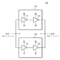
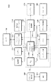
図1は本発明の実施形態によるレベル変換器100を示すブロック図である。図1を参照すれば、レベル変換器100は第1電圧変換回路110及び第2電圧変換回路120を含む。第1及び第2電圧変換回路110、120は入力ノードA及び出力ノードFの間に並列に連結される。
FIG. 1 is a block diagram illustrating a
第1電圧変換回路110は入力ノードAを通じて第1電圧V1に対応する第1電圧ドメインの第1クロックCLK1を受信する。第1クロックCLK1は第1電圧V1のスウィング(swing)幅を有することができる。第1電圧変換回路110は受信された第1クロックCLK1に基づいて、第2電圧V2に対応する第2電圧ドメインの信号を発生する。第2クロックCLK2は第2電圧V2のスウィング幅を有することができる。
The first
第1電圧変換回路110は第1及び第2インバータ111、113を含む。第1インバータ111は第1クロックCLK1に応じて第2電圧V2及び接地電圧VSSの中で1つを出力するように構成される。第2インバータ113は第1インバータ111の出力に応じて第2電圧V2及び接地電圧VSSの中で1つを出力するように構成される。即ち、第2インバータ113は第1クロックCLK1に同期される第2電圧ドメインの信号を出力する。
The first
第2電圧変換回路120は入力ノードAを通じて第1電圧ドメインの第1クロックCLK1を受信する。第1電圧変換回路110は受信された第1クロックCLK1に基づいて第2電圧ドメインの信号を発生する。
The second
第2電圧変換回路120は第1電圧変換回路110と同一な構造を有する。第2電圧変換回路120は第3及び第4インバータ121、123を含む。第3インバータ121は第1クロックCLK1に応じて第1電圧V1及び接地電圧VSSの中で1つを出力するように構成される。第4インバータ123は第3インバータ121の出力に応じて第2電圧V2及び接地電圧VSSの中で1つを出力するように構成される。即ち、第4インバータ123は第1クロックCLK1に同期される第2電圧ドメインの信号を出力する。
The second
第1及び第2電圧変換回路110、120は出力ノードFで混合される。第1電圧変換回路110は第1クロックCLK1に同期される第2電圧ドメインの信号を出力する。第2電圧変換回路120また第1クロックCLK1に同期される第2電圧ドメインの信号を出力する。即ち、出力ノードFで、第1クロックCLK1に同期される第2電圧ドメインの信号が生成される。出力ノードFの信号は第2電圧ドメインの第2クロックCLK2へ出力される。
The first and second
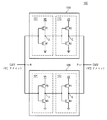
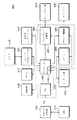
図2は本発明の実施形態によるレベル変換器100を示す回路図である。例示的に、図1を参照して説明された第1乃至第4インバータ111、113、121、123の内部回路が図示されている。例示的に、第1乃至第4インバータ111、113、121、123各々はCMOSインバータであり得る。しかし、第1乃至第4インバータ111、113、121、123の内部回路は図2に図示された回路に限定されない、
FIG. 2 is a circuit diagram illustrating a
図1及び図2を参照すれば、第1インバータ111は第1PMOSトランジスターP1及び第1NMOSトランジスターN1を含む。第1PMOSトランジスターP1のゲートは入力ノードAに連結される。第1PMOSトランジスターP1の一端へ第2電圧V2が供給され、他端は出力ノードBに連結される。第1NMOSトランジスターN1のゲートは入力ノードAに連結される。第1NMOSトランジスターN1の一端は接地ノードに連結され、他端は出力ノードBに連結される。
Referring to FIGS. 1 and 2, the
第2インバータ113は第1インバータ111と同一な構造を有する。第2インバータ113は第2PMOSトランジスターP2及び第2NMOSトランジスターN2を含む。第2PMOSトランジスターP2のゲートは第1インバータ111の出力ノードBに連結される。第2PMOSトランジスターP2の一端へ第2電圧V2が供給され、他端は出力ノードCに連結される。第2NMOSトランジスターN2のゲートは第1インバータ111の出力ノードBに連結される。第2NMOSトランジスターN2の一端は接地ノードに連結され、他端は出力ノードCに連結される。
The
第3インバータ121は第1インバータ111と同一な構造を有する。第3インバータ121は第3PMOSトランジスターP3及び第3NMOSトランジスターN3を含む。第3PMOSトランジスターP3のゲートは入力ノードAに連結される。第3PMOSトランジスターP3の一端へ第1電圧V1が供給され、他端は出力ノードDに連結される。第3NMOSトランジスターN3のゲートは入力ノードAに連結される。第3NMOSトランジスターN3の一端は接地ノードに連結され、他端は出力ノードDに連結される。
The
第4インバータ123は第1インバータ111と同一な構造を有する。第4インバータ123は第4PMOSトランジスターP4及び第4NMOSトランジスターN4を含む。第4PMOSトランジスターP4のゲートは第3インバータ121の出力ノードDに連結される。第4PMOSトランジスターP4の一端へ第2電圧V2が供給され、他端は出力ノードEに連結される。第4NMOSトランジスターN4のゲートは第3インバータ121の出力ノードDに連結される。第4NMOSトランジスターN4の一端は接地ノードに連結され、他端は出力ノードEに連結される。
The
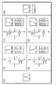
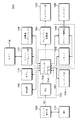
図3は第1クロックCLK1が立ち上がる時、図2を参照して説明された第1乃至第4インバータ111、113、121、123の動作を示す図面である。図2及び図3を参照すれば、第1クロックCLK1は接地電圧VSSから第1電圧V1に上昇する。第1クロックCLK1が第1電圧V1である時、第1インバータ111の第1PMOSトランジスターP1はターンオフされ、第1NMOSトランジスターN1はターンオンされる。即ち、第1インバータ111の出力ノードBは接地ノードに連結される。
FIG. 3 illustrates operations of the first to
第1クロックCLK1が接地電圧VSSである時、第1インバータ111の出力ノードBへ第1PMOSトランジスターP1を通じて第2電圧V2が供給される。したがって、第1クロックCLK1が接地電圧VSSから第1電圧V1に上昇する時、第1インバータ111の出力ノードBの電圧は第2電圧V2から接地電圧VSSへ放電される。
When the first clock CLK1 is the ground voltage VSS, the second voltage V2 is supplied to the output node B of the
具体的に、第1NMOSトランジスターN1のドレーンD1へ第2電圧V2が印加され、ゲートG1へ第1電圧V1が印加され、ソースS1へ接地電圧VSSが印加された状態で、第1NMOSトランジスターN1のチャンネルを通じて出力ノードBの電圧が放電される。この時、第1インバータ111の出力ノードBの電圧が接地電圧VSSへ放電されるのに所要される時間は第1時間T1であり得る。第1時間T1は第1インバータ111の出力ノードBの電圧が第1クロックCLK1の立ち上がりエッジ(rising edge)に同期されて立ち下がる時までの遅延時間であり得る。
Specifically, the channel of the first NMOS transistor N1 is applied with the second voltage V2 applied to the drain D1 of the first NMOS transistor N1, the first voltage V1 applied to the gate G1, and the ground voltage VSS applied to the source S1. Through which the voltage at the output node B is discharged. At this time, the time required for the voltage at the output node B of the
第1インバータ111の出力電圧が接地電圧VSSである時、第2インバータ113の第2NMOSトランジスターN2はターンオフされ、第2PMOSトランジスターP2はターンオンされる。即ち、第2インバータ113の出力ノードCへ第2電圧V2が供給される。
When the output voltage of the
第1インバータ111の出力電圧が第2電圧V2である時、第2インバータ113の出力ノードCへ第2NMOSトランジスターN2を通じて接地電圧VSSが供給される。したがって、第1インバータ111の出力電圧が第2電圧V2から接地電圧VSSに下降する時、第2インバータ113の出力ノードCの電圧は接地電圧VSSから第2電圧V2に充電される。
When the output voltage of the
具体的に、第2PMOSトランジスターP2のソースS2へ第2電圧V2が印加され、ゲートG2へ接地電圧VSSが印加され、ドレーンD2へ接地電圧VSSが印加された状態で、第2PMOSトランジスターP2のチャンネルを通じて出力ノードCの電圧が充電される。この時、第2インバータ113の出力ノードCの電圧が第2電圧V2に充電されるのに所要される時間は第2時間T2であり得る。第2時間T2は第2インバータ113の出力ノードCの電圧が第1インバータ111の出力電圧の立ち下がりエッジ(falling edge)に同期されて立ち上がる時までの遅延時間であり得る。
Specifically, the second voltage V2 is applied to the source S2 of the second PMOS transistor P2, the ground voltage VSS is applied to the gate G2, and the ground voltage VSS is applied to the drain D2, through the channel of the second PMOS transistor P2. The voltage at the output node C is charged. At this time, the time required for the voltage of the output node C of the
第1クロックCLK1は接地電圧VSSから第1電圧V1に上昇する。第1クロックCLK1が第1電圧V1である時、第3インバータ121の第3PMOSトランジスターP1はターンオフされ、第3NMOSトランジスターN3はターンオンされる。即ち、第3インバータ121の出力ノードDへ接地電圧VSSが供給される。
The first clock CLK1 rises from the ground voltage VSS to the first voltage V1. When the first clock CLK1 is the first voltage V1, the third PMOS transistor P1 of the
第1クロックCLK1が接地電圧VSSである時、第3インバータ121の出力ノードDへ第3PMOSトランジスターP3を通じて第1電圧V1が供給される。したがって、第1クロックCLK1が接地電圧VSSから第1電圧V1に上昇する時、第3インバータ121の出力ノードDの電圧は第1電圧V1から接地電圧VSSへ放電される。
When the first clock CLK1 is the ground voltage VSS, the first voltage V1 is supplied to the output node D of the
具体的に、第3NMOSトランジスターN3のドレーンD3へ第1電圧V1が印加され、ゲートG3へ第1電圧V1が印加され、ソースS3へ接地電圧VSSが印加された状態で、第3NMOSトランジスターN3のチャンネルを通じて出力ノードDの電圧が放電される。この時、第3インバータ121の出力ノードDの電圧が接地電圧VSSへ放電されるのに所要される時間は第3時間T3であり得る。第3時間T3は第3インバータ121の出力ノードDの電圧が第1クロックCLK1の立ち上がりエッジ(falling edge)に同期されて立ち下がる時までの遅延時間であり得る。
Specifically, the channel of the third NMOS transistor N3 is applied with the first voltage V1 applied to the drain D3 of the third NMOS transistor N3, the first voltage V1 applied to the gate G3, and the ground voltage VSS applied to the source S3. The voltage of the output node D is discharged through. At this time, the time required for the voltage at the output node D of the
第3インバータ121の出力が接地電圧VSSである時、第4インバータ123の第4NMOSトランジスターN4はターンオフされ、第4PMOSトランジスターP4はターンオンされる。即ち、第4インバータ123の出力ノードEへ第2電圧V2が供給される。
When the output of the
第3インバータ121の出力電圧が第1電圧V1である時、第4インバータ123の出力ノードEへ第4NMOSトランジスターN4を通じて接地電圧VSSが供給される。したがって、第3インバータ121の出力電圧が第1電圧V1から接地電圧VSSに下降する時、第4インバータ123の出力ノードEの電圧は接地電圧VSSから第2電圧V2に充電される。
When the output voltage of the
具体的に、第4PMOSトランジスターP4のソースS4へ第2電圧V2が印加され、ゲートG4へ接地電圧VSSが印加され、ドレーンD4へ接地電圧VSSが印加された状態で、第4PMOSトランジスターP4のチャンネルを通じて出力ノードEの電圧が充電される。この時、第4インバータ123の第4PMOSトランジスターP4のバイアス条件は第2インバータ113の第2PMOSトランジスターP2のバイアス条件と同一である。したがって、第4インバータ123の出力ノードEの電圧が第2電圧V2へ充電されるのに所要される時間は第2時間T2であり得る。第2時間T2は第4インバータ123の出力ノードEの電圧が第3インバータ121の出力電圧の立ち下がりエッジに同期されて立ち上がる時までの遅延時間であり得る。
Specifically, the second voltage V2 is applied to the source S4 of the fourth PMOS transistor P4, the ground voltage VSS is applied to the gate G4, and the ground voltage VSS is applied to the drain D4, and the channel of the fourth PMOS transistor P4. The voltage at the output node E is charged. At this time, the bias condition of the fourth PMOS transistor P4 of the
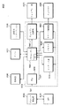
図4は第1クロックCLK1が立ち下がる時、図2を参照して説明された第1乃至第4インバータ111、113、121、123の動作を示す図面である。図2及び図4を参照すれば、第1クロックCLK1は第1電圧V1から接地電圧VSSに下降する。第1クロックCLK1が接地電圧VSSである時、第1インバータ111の第1NMOSトランジスターN1はターンオフされ、第1PMOSトランジスターP1はターンオンされる。即ち、第1インバータ111の出力ノードBへ第2電圧V2が供給される。
FIG. 4 illustrates operations of the first to
第1クロックCLK1が第1電圧V1である時、第1インバータ111の出力ノードBへ第1NMOSトランジスターN1を通じて接地電圧VSSが供給される。したがって、第1クロックCLK1が第1電圧V1から接地電圧VSSに下降する時、第1インバータ111の出力ノードBの電圧は接地電圧VSSから第2電圧V2に充電される。
When the first clock CLK1 is the first voltage V1, the ground voltage VSS is supplied to the output node B of the
具体的に、第1PMOSトランジスターP1のソースS5へ第2電圧V2が印加され、ゲートG6へ接地電圧VSSが印加され、ドレーンD6へ接地電圧VSSが印加された状態で、第1PMOSトランジスターP1のチャンネルを通じて出力ノードBの電圧が充電される。第1PMOSトランジスターP1のバイアス条件は図3を参照して説明された第2インバータ113の第2PMOSトランジスターP2のバイアス条件と同一である。したがって、第1インバータ111の出力ノードBの電圧が第2電圧V2に充電されるのに所要される時間は第2時間T2であり得る。第2時間T2は第1インバータ111の出力ノードBの電圧が第1クロックCLK1の立ち下がりエッジに同期されて立ち上がる時までの遅延時間であり得る。
Specifically, the second voltage V2 is applied to the source S5 of the first PMOS transistor P1, the ground voltage VSS is applied to the gate G6, and the ground voltage VSS is applied to the drain D6, and the channel of the first PMOS transistor P1. The voltage at the output node B is charged. The bias condition of the first PMOS transistor P1 is the same as the bias condition of the second PMOS transistor P2 of the
第1インバータ111の出力電圧が第2電圧V2である時、第2インバータ113の第2PMOSトランジスターP2はターンオフされ、第2NMOSトランジスターN2はターンオンされる。即ち、第2インバータ113の出力ノードCへ接地電圧VSSが供給される。
When the output voltage of the
第1インバータ111の出力電圧が接地電圧VSSである時、第2インバータ113の出力ノードCへ第2PMOSトランジスターP2を通じて第2電圧V2が供給される。したがって、第1インバータ111の出力電圧が接地電圧VSSから第2電圧V2に上昇した時に、第2インバータ113の出力ノードCの電圧は第2電圧V2から接地電圧VSSへ放電される。
When the output voltage of the
具体的に、第2NMOSトランジスターN2のドレーンD7へ第2電圧V2が印加され、ゲートG7へ第2電圧V2が印加され、ソースS7へ接地電圧VSSが印加された状態で、第2NMOSトランジスターN2のチャンネルを通じて出力ノードCの電圧が放電される。 Specifically, the channel of the second NMOS transistor N2 is applied with the second voltage V2 applied to the drain D7 of the second NMOS transistor N2, the second voltage V2 applied to the gate G7, and the ground voltage VSS applied to the source S7. The voltage of the output node C is discharged through.
この時、トランジスターの種類がNMOSトランジスターであることを除外すれば、第2NMOSトランジスターN2のバイアス条件は第1インバータ111の第1PMOSトランジスターP1のバイアス条件と同一である。第2NMOSトランジスターN2のゲート−ソース電圧差は第2電圧V2であり、第1PMOSトランジスターP1のゲート−ソース電圧差また第2電圧V2である。第2NMOSトランジスターN2のドレーン−ソース電圧差は第2電圧V2であり、第1PMOSトランジスターP1のドレーン−ソース電圧差また第2電圧V2である。
At this time, except that the type of transistor is an NMOS transistor, the bias condition of the second NMOS transistor N2 is the same as the bias condition of the first PMOS transistor P1 of the
第1乃至第4インバータ111、113、121、123各々は1つのPMOSトランジスター及び1つのNMOSトランジスターを含む。第1乃至第4インバータ111、113、121、123の入力電圧が低レベルである時、第1乃至第4インバータ111、113、121、123の出力電圧はPMOSトランジスターP1〜P4によって生成される。第1乃至第4インバータ111、113、121、123の入力電圧が高レベルである時、第1乃至第4インバータ111、113、121、123の出力電圧はNMOSトランジスターN1〜N4によって生成される。
Each of the first to
低レベル出力及び高レベル出力を有するように、第1乃至第4インバータ111、113、121、123が形成され得る。例えば、高レベルを出力する時、充電する電流量と低レベルを出力する時、放電する電流量とが平準化されるように、第1乃至第4インバータ111、113、121、123が形成され得る。同一なバイアス条件で、第1乃至第4NMOSトランジスターN1〜N4は第1乃至第4PMOSトランジスターP1〜P4と同様に動作するように形成され得る。同一なバイアス条件で、第2NMOSトランジスターN2を通じて流れる電流の量は第1PMOSトランジスターP1を通じて流れる電流の量と同一であり得る。
The first to
第2NMOSトランジスターN2のバイアス条件が第1PMOSトランジスターP1のバイアス条件と同一であるので、第2インバータ113の出力ノードCの電圧が接地電圧VSSへ放電されるのに所要される時間は第2時間T2であり得る。第2時間T2は第2インバータ113の出力ノードCの電圧が第1インバータ111の出力電圧の立ち上がりエッジに同期されて立ち下がる時までの遅延時間であり得る。
Since the bias condition of the second NMOS transistor N2 is the same as the bias condition of the first PMOS transistor P1, the time required for the voltage at the output node C of the
第1クロックCLK1が接地電圧VSSである時、第3インバータ121の第3NMOSトランジスターN1はターンオフされ、第3PMOSトランジスターP3はターンオンされる。即ち、第3インバータ121の出力ノードDへ第1電圧V1が供給される。
When the first clock CLK1 is at the ground voltage VSS, the third NMOS transistor N1 of the
第1クロックCLK1が第1電圧V1である時、第3インバータ121の出力ノードDへ第3NMOSトランジスターN3を通じて接地電圧VSSが供給される。したがって、第1クロックCLK1が第1電圧V1から接地電圧VSSに下降する時、第3インバータ121の出力ノードDの電圧は接地電圧VSSから第1電圧V1に充電される。
When the first clock CLK1 is the first voltage V1, the ground voltage VSS is supplied to the output node D of the
具体的に、第3PMOSトランジスターP3のソースS7へ第1電圧V1が印加され、ゲートG7へ接地電圧VSSが印加され、ドレーンD7へ接地電圧VSSが印加された状態で、第3PMOSトランジスターP3のチャンネルを通じて出力ノードDの電圧が充電される。 Specifically, the first voltage V1 is applied to the source S7 of the third PMOS transistor P3, the ground voltage VSS is applied to the gate G7, and the ground voltage VSS is applied to the drain D7, and the channel of the third PMOS transistor P3 is applied. The voltage at the output node D is charged.
この時、トランジスターの種類がPMOSトランジスターであることを除外すれば、第3PMOSトランジスターP2のバイアス条件は図3を参照して説明された第3NMOSトランジスターN3のバイアス条件と同一である。第3PMOSトランジスターP3のゲート−ソース電圧差は第1電圧V1であり、第3NMOSトランジスターN3のゲート−ソース電圧差また第1電圧V1である。第3PMOSトランジスターP3のドレーン−ソース電圧差は第1電圧V1であり、第3NMOSトランジスターN3のドレーン−ソース電圧差また第1電圧V1である。 At this time, except that the type of transistor is a PMOS transistor, the bias condition of the third PMOS transistor P2 is the same as the bias condition of the third NMOS transistor N3 described with reference to FIG. The gate-source voltage difference of the third PMOS transistor P3 is the first voltage V1, and the gate-source voltage difference or the first voltage V1 of the third NMOS transistor N3. The drain-source voltage difference of the third PMOS transistor P3 is the first voltage V1, and the drain-source voltage difference or the first voltage V1 of the third NMOS transistor N3.
したがって、第3インバータ121の出力ノードDの電圧が第1電圧V1に充電されるのに所要される時間は第3時間T3であり得る。第3時間T3は第3インバータ121の出力ノードDの電圧が第1クロックCLK1の立ち下がりエッジに同期されて立ち上がる時までの遅延時間であり得る。
Therefore, the time required for the voltage at the output node D of the
第3インバータ121の出力電圧が第1電圧V1である時、第4インバータ123の第4PMOSトランジスターP4はターンオフされ、第4NMOSトランジスターN4はターンオンされる。即ち、第4インバータ123の出力ノードEへ接地電圧VSSが供給される。
When the output voltage of the
第3インバータ121の出力電圧が接地電圧VSSである時、第4インバータ123の出力ノードEへ第4PMOSトランジスターP4を通じて第2電圧V2が供給される。したがって、第3インバータ121の出力電圧が接地電圧VSSから第1電圧V1に上昇する時、第4インバータ123の出力ノードEの電圧は第2電圧V2から接地電圧VSSへ放電される。
When the output voltage of the
具体的に、第4NMOSトランジスターN4のドレーンD8へ第2電圧V2が印加され、ゲートG8へ第1電圧V1が印加され、ソースS8へ接地電圧VSSが印加された状態で、第4PMOSトランジスターP4のチャンネルを通じて出力ノードEの電圧が放電される。 Specifically, the channel of the fourth PMOS transistor P4 is applied with the second voltage V2 applied to the drain D8 of the fourth NMOS transistor N4, the first voltage V1 applied to the gate G8, and the ground voltage VSS applied to the source S8. The voltage of the output node E is discharged through.
この時、第4インバータ123の第4NMOSトランジスターN4のバイアス条件は図3を参照して説明された第1NMOSトランジスターN1のバイアス条件と同一である。したがって、第4インバータ123の出力ノードEの電圧が接地電圧VSSへ放電されるのに所要される時間は第1時間T1であり得る。第1時間T1は第4インバータ123の出力ノードEの電圧が第3インバータ121の出力電圧の立ち上がりエッジに同期されて立ち下がる時までの遅延時間であり得る。
At this time, the bias condition of the fourth NMOS transistor N4 of the
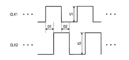
図5は図1乃至図4を参照して説明されたレベル変換器100の入力クロックCLK1及び出力クロックCLK2を示すタイミング図である。図1乃至図5を参照すれば、第1クロックCLK1がレベル変換器100へ入力される。第1クロックCLK1は第1電圧V1のスウィング幅を有する。第1クロックCLK1は周期的に反複される立ち上がりエッジ及び立ち下がりエッジを有する。
FIG. 5 is a timing diagram showing the input clock CLK1 and the output clock CLK2 of the
第2クロックCLK2がレベル変換器100から出力される。第2クロックCLK2は第2電圧V2のスウィング幅を有する。第1クロックCLK1の立ち上がりエッジに同期されて、第2クロックCLK2が立ち上がる。第2クロックCLK2は第1電圧変換回路110の第1及び第2インバータ111、113の充電と放電、及び第2電圧変換回路120の第3及び第4インバータ121、123の充電と放電によって上昇する。
The second clock CLK2 is output from the
図3を参照して説明されたように、第1クロックCLK1が上昇し、第1時間T1後に、第1インバータ111の出力電圧が減少して接地電圧VSSに到達する。第1インバータ111の出力電圧が下降し、第2時間T2後に、第2インバータ113の出力電圧が増加して第2電圧V2に到達する。第1クロックCLK1が上昇し、第3時間T3後に、第3インバータ121の出力電圧が下降して接地電圧VSSに到達する。第3インバータ121の出力電圧が下降し、第2時間T2後に、第4インバータ123の出力電圧が上昇して第2電圧V2に到達する。
As described with reference to FIG. 3, the first clock CLK1 rises, and after the first time T1, the output voltage of the
第2及び第4インバータ113、123の出力電圧が混合されて第2クロックCLK2が形成される。即ち、第1クロックCLK1の立ち上がりエッジと第2クロックCLK2の立ち上がりエッジとの間の遅延D1は第1時間T1、第2時間T2、及び第3時間T3が加算されて発生される。
The output voltages of the second and
図4を参照して説明されたように、第1クロックCLK1が下降し、第2時間T2後に、第1インバータ111の出力電圧が上昇して第2電圧V2に到達する。第1インバータ111の出力電圧が上昇し、第2時間T2後に、第2インバータ113の出力電圧が下降して接地電圧VSSに到達する。第1クロックCLK1が下降し、第3時間T3後に、第3インバータ121の出力電圧が上昇して第1電圧V1に到達する。第3インバータ121の出力電圧が上昇し、第1時間T1後に、第4インバータ123の出力電圧が下降して接地電圧VSSに到達する。
As described with reference to FIG. 4, the first clock CLK1 falls, and after the second time T2, the output voltage of the
第2及び第4インバータ113、123の出力電圧が混合されて、第2クロックCLK2が形成される。即ち、第1クロックCLKの立ち下がりエッジと第2クロックCLK2の立ち下がりエッジの間の遅延D2は第1時間T1、第2時間T2、及び第3時間T3が加算されて発生される。
The output voltages of the second and
上述したように、第1及び第2クロックCLK1、CLK2の立ち上がりエッジの間の遅延D1を発生させる時間要因T1、T2、T3は立ち下がりエッジの間の遅延D2を発生させる時間要因T1、T2、T3と同一である。したがって、第1及び第2クロックCLK1、CLK2の立ち上がりエッジの間の遅延D1と立ち下がりエッジの間の遅延D2とは同一であり得る。 As described above, the time factors T1, T2, and T3 that generate the delay D1 between the rising edges of the first and second clocks CLK1 and CLK2 are the time factors T1, T2, and T2, that generate the delay D2 between the falling edges. It is the same as T3. Accordingly, the delay D1 between the rising edges of the first and second clocks CLK1 and CLK2 and the delay D2 between the falling edges may be the same.
立ち上がりエッジの間の遅延D1と立ち下がりエッジの間の遅延D2とが互に異なる場合、第2クロックCLK2の一周期の高レベル区間と低レベル区間との比率が可変され得る。 When the delay D1 between the rising edges and the delay D2 between the falling edges are different from each other, the ratio between the high level section and the low level section of one cycle of the second clock CLK2 can be varied.
例示的に、立ち上がりエッジの間の遅延D1が立ち下がりエッジの間の遅延D2より大きい場合、第2クロックCLK2の一周期の高レベル区間の比率は第1クロックCLK1の一周期の高レベル区間の比率より減少する。反対に、立ち下がりエッジの間の遅延D2が立ち上がりエッジの間の遅延D1より大きい場合、第2クロックCLK2の一周期の低レベル区間の比率は第1クロックCLK1の一周期の低レベル区間の比率より減少する。本発明の実施形態によれば、レベル変換器100は高レベル及び低レベル区間の比率(Duty ratio)を維持し、入力される第1クロックCLK1と他の電圧ドメインの第2クロックCLK2とを発生できる。したがって、レベル変換器100の出力クロックの信頼性が向上され得る。
Exemplarily, when the delay D1 between the rising edges is larger than the delay D2 between the falling edges, the ratio of the high level interval of one cycle of the second clock CLK2 is the ratio of the high level interval of one cycle of the first clock CLK1. Decrease from the ratio. On the contrary, when the delay D2 between the falling edges is larger than the delay D1 between the rising edges, the ratio of the low level section of one cycle of the second clock CLK2 is the ratio of the low level section of one cycle of the first clock CLK1. Decrease more. According to the embodiment of the present invention, the
例示的に、第2電圧V2は第1電圧V1より低いか、或いは高いことができる。 For example, the second voltage V2 may be lower or higher than the first voltage V1.
図6は図1乃至図5を参照して説明されたレベル変換器100を含むシステムオンチップ500(SOC、System−On−Chip)を示すブロック図である。図6を参照すれば、システムオンチップ500はプロセッサー510、位相ロックループ520、周辺ブロック530、オーディオブロック540、ディスプレーブロック550、グラフィックブロック560、イメージプロセシングブロック570、及びコーデックブロック580を含む。
FIG. 6 is a block diagram illustrating a system-on-chip 500 (SOC, System-On-Chip) including the
プロセッサー510は第1乃至第8フリップフロップ512〜519を含む。プロセッサー510はレベル変換器100をさらに包含するか、又はレベル変換器100に連結され得る。レベル変換器100は位相ロックループ520から第1クロックCLK1を受信する。第1クロックCLK1は第1電圧V1のスウィングを有することができる。レベル変換器100は高レベル及び低レベル区間の比率を維持し、第1クロックCLK1に同期される第2クロックCLK2を発生する。第2クロックCLK2は第2電圧V1のスウィングを有することができる。第2電圧V2は第1電圧V1より大きくなり得る。
The
レベル変換器100で発生された第2クロックCLK2はプロセッサー510のフリップフロップ512〜519へ供給される。プロセッサー510のフリップフロップ512〜519は第2クロックCLK2に応じて動作する。
The second clock CLK2 generated by the
位相ロックループ520は外部からクロックCLKを受信する。位相ロックループ520は受信されたクロックCLKと同期される第1クロックCLK1を発生する。第1クロックCLK1はプロセッサー510のレベル変換器100、周辺ブロック530、オーディオブロック540、ディスプレーブロック550、グラフィックブロック560、イメージプロセシングブロック570、及びコーデックブロック580へ供給される。
The
周辺ブロック530、オーディオブロック540、ディスプレーブロック550、グラフィックブロック560、イメージプロセシングブロック570、及びコーデックブロック580は第1クロックCLK1に応じて動作する。周辺ブロック530、オーディオブロック540、ディスプレーブロック550、グラフィックブロック560、イメージプロセシングブロック570、及びコーデックブロック580はIP(Intellectual Property)であり得る。
The
オーディオブロック540はオーディオデータを処理できる。ディスプレーブロック550はモニター(図示せず)のようなディスプレー装置を制御する信号を発生できる。グラフィックブロック560はモニター(図示せず)のようなディスプレー装置に表示されるグラフィックデータを処理できる。イメージプロセシングブロック570はカメラ(図示せず)のような撮影装置によって撮影されるイメージデータを処理できる。コーデック580はオーディオデータのエンコーディング又はデコーディングを遂行できる。コーデック580はグラフィックデータのエンコーディング又はデコーディングを遂行できる。
図6に示したように、システムオンチップ500の周辺ブロック530、オーディオブロック540、ディスプレーブロック550、グラフィックブロック560、イメージプロセシングブロック570、及びコーデックブロック580は第1クロックCLK1に応じて動作する。プロセッサー510は第1電圧ドメインの第1クロックCLK1が変換された第2電圧ドメインの第2クロックCLK2に応じて動作できる。第2電圧V2は第1電圧V1より高いことができる。
As shown in FIG. 6, the
レベル変換器100は図1乃至図5を参照して説明されたレベル変換器100であり得る。例示的に、レベル変換器100は入力ノードAと出力ノードFとの間に並列に連結され、同一な構造を有する第1及び第2電圧変換回路110、120を包含できる。レベル変換器100の入力クロックCLK1と出力クロックCLK2との立ち上がりエッジの間の遅延D1と立ち下がりエッジの間の遅延D2とは同一であり得る。したがって、第2クロックCLK2に応じて動作するプロセッサー510の信頼性、及びプロセッサー510を含むシステムオンチップ500の信頼性が向上される。
The
プロセッサー510が高速に動作するように設計される場合、プロセッサー510は第2クロックCLK2の立ち上がりエッジと立ち下がりエッジとの全てに同期されて動作できる。本発明の実施形態によるレベル変換器100は高レベル区間及び低レベル区間の比率を維持し、第1電圧ドメインの第1クロックCLK1を第2電圧ドメインの第2クロックCLK2に変換する。高レベル区間及び低レベル区間の比率が維持されれば、第2クロックCLK2の立ち上がりエッジと立ち下がりエッジとのマージン(margin)が最適化されて維持され得る。したがって、本発明の実施形態によるレベル変換器100が提供される時、第2クロックCLK2の立ち上がりエッジと立ち下がりエッジとの全てに同期されて動作するプロセッサー510及びシステムオンチップ500の信頼性が向上され得る。
When the
図7は本発明の実施形態によるレベル変換器100を含むマルチメディア装置1000の第1例を示すブロック図である。図7を参照すれば、マルチメディア装置1000は発振器1010、クロック発生部1020、位相ロックループ1030、プロセッサー1040、メモリー1050、ディスプレー制御部1060、ディスプレー部1070、サウンド制御部1080、スピーカー1090、格納部1100、モデム1110、イメージプロセシング部1120、カメラ1130、使用者インターフェイス1140、及びコーデック部1150を含む。
FIG. 7 is a block diagram illustrating a first example of a
発振器1010は特定周波数にしたがって発振する発振信号を発生する。発振信号はクロック発生部1020へ供給される。
The
クロック発生部1020は発振器1010から供給される発振信号に応じてクロック1020を発生する。クロックCLKは位相ロックループ1030へ供給され得る。
The
位相ロックループ1030はクロック発生部1020から受信されるクロックCLKに応じて第1クロックCLK1を発生するように構成される。第1クロックCLK1は受信されたクロックCLKと同期され得る。第1クロックCLK1はプロセッサー1040へ供給され得る。
The phase locked
プロセッサー1040はマルチメディア装置1000の諸般動作を制御するように構成される。プロセッサー1040はマルチメディア装置1000のハードウェア構成要素を制御する。プロセッサー1040はマルチメディア装置1000のソフトウェア構成要素を駆動する。
The
プロセッサー1040は本発明の実施形態によるレベル変換器100を包含するか、又はレベル変換器100に連結され得る。レベル変換器100は位相ロックループ1030から供給される第1電圧ドメインの第1クロックCLK1に基づいて、第2電圧ドメインの第2クロックCLK2を発生する。第2クロックCLK2はプロセッサー1010の内部クロックに使用される。
The
メモリー1050はプロセッサー1040の動作メモリーであり得る。例示的に、メモリー1050はSRAM(Static RAM)、DRAM(Dynamic RAM)、SDRAM(Synchronous DRAM)等のような揮発性メモリー、又はフラッシュメモリー、PRAM(Phase−change RAM)、MRAM(Magnetic RAM)、RRAM(Resistive RAM)(登録商標)、FRAM(Ferroelectric RAM)(登録商標)等のような不揮発性メモリーを包含できる。
ディスプレー制御部1060はプロセッサー1040の制御にしたがって動作する。ディスプレー制御部1060はディスプレー部1070を通じて表示される映像を生成及び制御するように構成される。ディスプレー制御部1060はグラフィック処理ユニット(GPU、Graphic Processing Unit)を包含できる。
The
ディスプレー部1070はディスプレー制御部1060によって生成された映像を表示するように構成される。ディスプレー部1070は液晶ディスプレー(LCD、Liquid Crystal Display)、有機発光ダイオード(OLED、Organic Light Emitting Diode)ディスプレー、アクティブマトリックス有機発光ダイオード(AMOLED、Active Matrix Organic Light Emitting Diode)ディスプレー、電子紙(electronic paper)等を包含できる。
The
サウンド制御部1080はプロセッサー1040の制御にしたがって動作する。サウンド制御部1080はスピーカー1090を通じて出力されるサウンドを生成及び制御することができる。スピーカー1090はサウンド制御部1080のサウンド制御部1080はプロセッサー1040の制御にしたがって動作する。サウンド制御部1080はスピーカー1090を通じて出力されるサウンドを生成及び制御することができる。スピーカー1090はサウンド制御部1080の制御にしたがってサウンドを出力することができる。
The
格納部1100はプロセッサー1040の制御にしたがって、データを格納するように構成される。格納部1100はフラッシュメモリー、PRAM(Phase−change RAM)、MRAM(Magnetic RAM)、RRAM(Resistive RAM)(登録商標)、FRAM(Ferroelectric RAM)(登録商標)等のような不揮発性メモリーを包含できる。格納部1100はハードディスクドライブHDD、Hard Disk Drive)、ソリッドステートドライブ(SSD、Solid State Drive)を包含できる。
The storage unit 1100 is configured to store data under the control of the
モデム1110はプロセッサー1040の制御にしたがって外部と通信できる。例示的に、モデム1110は無線チャンネル又は有線チャンネルを通じて外部と通信できる。モデム1110はCDMA(Code Division Multiple Access)、GSM(Global System for Mobile communications)(登録商標)、CDMA 2000、WCDMA(Wideband Code Division Multiple Access)、LTE (Long Term Evolution)、WiBro(Wireless Broadband Internet)、Mobile WiMAX(World Interoperability)、WiFi等のような無線プロトコルにしたがって、外部と通信できる。モデム1110は ADSL(Asymmetric Digital Subscriber Line)、VDSL(Very high data rate Digital Subscriber Line)、ISDN(Integrated Services Digital Network)等のような有線プロトコルにしたがって、外部と通信できる。
The modem 1110 can communicate with the outside according to the control of the
イメージプロセシング部1130はプロセッサー1040の制御に応じて動作する。イメージプロセシング部1130はカメラ1140によって撮影又は録画されるイメージデータを処理するように構成される。
The
使用者インターフェイス1140は外部から感知される信号をプロセッサー1140へ伝達するように構成される。例示的に、使用者インターフェイス1120はマイクロフォン(microphone)、タッチパッド(touch pad)、タッチスクリーン(touch screen)、ボタン、マウス、キーボード等を包含できる。
The
コーデック部1150はオーディオデータをエンコーディング又はデコーディングできる。コーデック部1150はビデオデータをエンコーディング又はデコーディングできる。 The codec unit 1150 can encode or decode audio data. The codec unit 1150 can encode or decode video data.
例示的に、位相ロックループ1030、プロセッサー1040、メモリー1050、ディスプレー制御部1060、サウンド制御部1080、イメージプロセシング部1120、及びコーデック部1150はシステムオンチップ1200を構成することができる。システムオンチップ1200は図6を参照して説明された構造を有することができる。プロセッサー1040は図6のプロセッサー510に対応することができる。メモリー1050は図6の周辺ブロック530に対応することができる。ディスプレー制御部1060は図6のディスプレーブロック550及びグラフィックブロック560に対応することができる。サウンド制御部1080は図6のオーディオブロック540に対応することができる。イメージプロセシング部1120は図6のイメージプロセシングブロック570に対応することができる。コーデック部1150は図6のコーデックブロック580に対応することができる。
For example, the
クロック発生部1020は発生されたクロックCLKをシステムオンチップ1200へ供給し、マルチメディア装置1000の構成要素の中でクロックCLKを必要とする他の構成要素へ供給することができる。
The
システムオンチップ1200の位相ロックループ1030は受信されたクロックCLKに同期する第1クロックCLK1を発生する。レベル変換器100は、図1乃至図5を参照して説明されたように、高レベル区間及び低レベル区間の比率を維持し、第1クロックCLK1に基づいて第2クロックCLK2を発生できる。プロセッサー1040は第2クロックCLK2に基づいて動作できる。システムオンチップ1200の他の構成要素、即ち、メモリー1050、ディスプレー制御部1060、サウンド制御部1080、イメージプロセシング部1120、及びコーデック部1150は第1クロックCLK1に応じて動作できる。
The phase-locked
図8は本発明の実施形態によるレベル変換器100を含むマルチメディア装置2000の第2実施形態を示すブロック図である。図8を参照すれば、マルチメディア装置2000は発振器2010、クロック発生部2020、位相ロックループ2030、プロセッサー2040、メモリー2050、ディスプレー制御部2060、ディスプレー部2070、サウンド制御部2080、スピーカー2090、格納部2100、モデム2110、イメージプロセシング部2120、カメラ2130、使用者インターフェイス2140、及びコーデック部2150を含む。
FIG. 8 is a block diagram illustrating a second embodiment of a
図7を参照して説明されたマルチメディア装置1000と比較すれば、マルチメディア装置2000で位相ロックループ2030、プロセッサー2040、メモリー2050、ディスプレー制御部2060、サウンド制御部2080、モデム2110、イメージプロセシング部2120、及びコーデック部2150がシステムオンチップ2200を構成することができる。システムオンチップ2200は図6を参照して説明された構造を有することができる。プロセッサー2040は図6のプロセッサー510に対応することができる。メモリー2050及びモデム2110は図6の周辺ブロック530に対応することができる。ディスプレー制御部2060は図6のディスプレーブロック550及びグラフィックブロック560に対応することができる。サウンド制御部2080は図6のオーディオブロック540に対応することができる。イメージプロセシング部2120は図6のイメージプロセシングブロック570に対応することができる。コーデック部2150は図6のコーデックブロック580に対応することができる。
Compared with the
クロック発生部2020は発生されたクロックCLKをシステムオンチップ2200へ供給し、マルチメディア装置2000の構成要素の中でクロックCLKを必要とする他の構成要素へ供給することができる。
The
システムオンチップ2200の位相ロックループ2030は受信されたクロックCLKに同期する第1クロックCLK1を発生する。レベル変換器100は、図1乃至図5を参照して説明されたように、高レベル区間及び低レベル区間の比率を維持し、第1クロックCLK1に基づいて第2クロックCLK2を発生できる。プロセッサー2040は第2クロックCLK2に基づいて動作できる。システムオンチップ2200の他の構成要素、即ち、メモリー2050、ディスプレー制御部2060、サウンド制御部2080、モデム2110、イメージプロセシング部2120、及びコーデック部2150は第1クロックCLK1に応じて動作できる。
The phase-locked
図9は本発明の実施形態によるレベル変換器100を含むマルチメディア装置3000の第3実施形態を示すブロック図である。図9を参照すれば、マルチメディア装置3000は発振器3010、クロック発生部3020、位相ロックループ3030、プロセッサー3040、メモリー3050、ディスプレー制御部3060、ディスプレー部3070、サウンド制御部3080、スピーカー3090、格納部3100、モデム3110、イメージプロセシング部3120、カメラ3130、使用者インターフェイス3140、及びコーデック部3150を含む。
FIG. 9 is a block diagram illustrating a third embodiment of a
図7を参照して説明されたマルチメディア装置1000と比較すれば、マルチメディア装置3000で位相ロックループ3030、プロセッサー3040、メモリー3050、ディスプレー制御部3060、サウンド制御部3080、及びコーデック部3150がシステムオンチップ2200を構成することができる。
Compared with the
クロック発生部3020は発生されたクロックCLKをシステムオンチップ3200へ供給し、マルチメディア装置3000の構成要素の中でクロックCLKを必要とする他の構成要素へ供給することができる。
The
システムオンチップ3200の位相ロックループ3030は受信されたクロックCLKに同期する第1クロックCLK1を発生する。レベル変換器100は、図1乃至図5を参照して説明されたように、高レベル区間及び低レベル区間の比率を維持し、第1クロックCLK1に基づいて第2クロックCLK2を発生できる。プロセッサー3040は第2クロックCLK2に基づいて動作できる。システムオンチップ3200の他の構成要素、即ち、メモリー3050、ディスプレー制御部3060、サウンド制御部3080、及びコーデック部3150は第1クロックCLK1に応じて動作できる。
The
図10は本発明の実施形態によるレベル変換器100を含むマルチメディア装置4000の第4実施形態を示すブロック図である。図10を参照すれば、マルチメディア装置4000は発振器4010、クロック発生部4020、位相ロックループ4030、プロセッサー4040、メモリー4050、ディスプレー制御部4060、ディスプレー部4070、サウンド制御部4080、スピーカー4090、格納部4100、モデム4110、イメージプロセシング部4120、カメラ4130、使用者インターフェイス4140、及びコーデック部4150を含む。
FIG. 10 is a block diagram illustrating a fourth embodiment of a
図7を参照して説明されたマルチメディア装置1000と比較すれば、マルチメディア装置4000で位相ロックループ4030、プロセッサー4040、メモリー4050、ディスプレー制御部4060、及びサウンド制御部4080がシステムオンチップ4200を構成することができる。
Compared with the
クロック発生部4020は発生されたクロックCLKをシステムオンチップ4200へ供給し、マルチメディア装置4000の構成要素の中でクロックCLKを必要とする他の構成要素へ供給することができる。
The
システムオンチップ4200の位相ロックループ4030は受信されたクロックCLKに同期する第1クロックCLK1を発生する。レベル変換器100は、図1乃至図5を参照して説明されたように、高レベル区間及び低レベル区間の比率を維持し、第1クロックCLK1に基づいて第2クロックCLK2を発生できる。プロセッサー4040は第2クロックCLK2に基づいて動作できる。システムオンチップ4200の他の構成要素、即ち、メモリー4050、ディスプレー制御部4060、及びサウンド制御部4080は第1クロックCLK1に応じて動作できる。
The phase-locked
図11は本発明の実施形態によるレベル変換器100を含むマルチメディア装置5000の第5実施形態を示すブロック図である。図11を参照すれば、マルチメディア装置5000は発振器5010、クロック発生部5020、位相ロックループ5030、プロセッサー5040、メモリー5050、ディスプレー制御部5060、ディスプレー部5070、サウンド制御部5080、スピーカー5090、格納部5100、モデム5110、イメージプロセシング部5120、カメラ5130、使用者インターフェイス5140、及びコーデック部5150を含む。
FIG. 11 is a block diagram illustrating a fifth embodiment of a
図7を参照して説明されたマルチメディア装置1000と比較すれば、マルチメディア装置5000で位相ロックループ5030、プロセッサー5040、メモリー5050、及びディスプレー制御部5060がシステムオンチップ5200を構成することができる。
Compared with the
クロック発生部5020は発生されたクロックCLKをシステムオンチップ5200へ供給し、マルチメディア装置5000の構成要素の中でクロックCLKを必要とする他の構成要素へ供給することができる。
The
システムオンチップ5200の位相ロックループ5030は受信されたクロックCLKに同期する第1クロックCLK1を発生する。レベル変換器100は、図1乃至図5を参照して説明されたように、高レベル区間及び低レベル区間の比率を維持し、第1クロックCLK1に基づいて第2クロックCLK2を発生できる。プロセッサー5040は第2クロックCLK2に基づいて動作できる。システムオンチップ5200の他の構成要素、即ち、メモリー5050及びディスプレー制御部5060は第1クロックCLK1に応じて動作できる。
The phase-locked
図12は本発明の実施形態によるレベル変換器100を含むマルチメディア装置6000の第6実施形態を示すブロック図である。図12を参照すれば、マルチメディア装置6000は発振器6010、クロック発生部6020、位相ロックループ6030、プロセッサー6040、メモリー6050、ディスプレー制御部6060、ディスプレー部6070、サウンド制御部6080、スピーカー6090、格納部6100、モデム6110、イメージプロセシング部6120、カメラ6130、使用者インターフェイス6140、及びコーデック部6150を含む。
FIG. 12 is a block diagram illustrating a sixth embodiment of a
図7を参照して説明されたマルチメディア装置1000と比較すれば、マルチメディア装置6000で位相ロックループ6030、プロセッサー6040、及びメモリー6050がシステムオンチップ6200を構成することができる。
Compared with the
クロック発生部6020は発生されたクロックCLKをシステムオンチップ6200へ供給し、マルチメディア装置6000の構成要素の中でクロックCLKを必要とする他の構成要素へ供給することができる。
The
システムオンチップ6200の位相ロックループ6030は受信されたクロックCLKに同期する第1クロックCLK1を発生する。レベル変換器100は、図1乃至図5を参照して説明されたように、高レベル区間及び低レベル区間の比率を維持し、第1クロックCLK1に基づいて第2クロックCLK2を発生できる。プロセッサー6040は第2クロックCLK2に基づいて動作できる。システムオンチップ6200の他の構成要素、即ち、メモリー6050は第1クロックCLK1に応じて動作できる。
The phase-locked
図13は本発明の実施形態によるレベル変換器100を含むマルチメディア装置7000の第7実施形態を示すブロック図である。図13を参照すれば、マルチメディア装置7000は発振器7010、クロック発生部7020、位相ロックループ7030、プロセッサー7040、メモリー7050、ディスプレー制御部7060、ディスプレー部7070、サウンド制御部7080、スピーカー7090、格納部7100、モデム7110、イメージプロセシング部7120、カメラ7130、使用者インターフェイス7140、及びコーデック部7150を含む。
FIG. 13 is a block diagram illustrating a seventh embodiment of a
図7を参照して説明されたマルチメディア装置1000と比較すれば、マルチメディア装置7000で位相ロックループ7030、プロセッサー7040、メモリー7050、及びサウンド制御部7080がシステムオンチップ7200を構成することができる。
Compared with the
クロック発生部7020は発生されたクロックCLKをシステムオンチップ7200へ供給し、マルチメディア装置7000の構成要素の中でクロックCLKを必要とする他の構成要素へ供給することができる。
The
システムオンチップ7200の位相ロックループ7030は受信されたクロックCLKに同期する第1クロックCLK1を発生する。レベル変換器100は、図1乃至図5を参照して説明されたように、高レベル区間及び低レベル区間の比率を維持し、第1クロックCLK1に基づいて第2クロックCLK2を発生できる。プロセッサー7040は第2クロックCLK2に基づいて動作できる。システムオンチップ7200の他の構成要素、即ち、メモリー7050及びサウンド制御部7080は第1クロックCLK1に応じて動作できる。
The phase-locked
図14は本発明の実施形態によるレベル変換器100を含むマルチメディア装置8000の第8実施形態を示すブロック図である。図14を参照すれば、マルチメディア装置8000は発振器8010、クロック発生部8020、位相ロックループ8030、プロセッサー8040、メモリー8050、ディスプレー制御部8060、ディスプレー部8070、サウンド制御部8080、スピーカー8090、格納部8100、モデム8110、使用者インターフェイス8140、及びコーデック部8150を含む。
FIG. 14 is a block diagram illustrating an eighth embodiment of a
図7を参照して説明されたマルチメディア装置1000と比較すれば、マルチメディア装置8000でイメージプロセシング部1120及びカメラ1130が提供されないことがある。及び、位相ロックループ8030、プロセッサー8040、メモリー8050、ディスプレー制御部8060、サウンド制御部8080、及びコーデック部8150がシステムオンチップ7200を構成することができる。
Compared to the
クロック発生部8020は発生されたクロックCLKをシステムオンチップ8200へ供給し、マルチメディア装置8000の構成要素の中でクロックCLKを必要とする他の構成要素へ供給することができる。
The
システムオンチップ8200の位相ロックループ8030は受信されたクロックCLKに同期する第1クロックCLK1を発生する。レベル変換器100は、図1乃至図5を参照して説明されたように、高レベル区間及び低レベル区間の比率を維持し、第1クロックCLK1に基づいて第2クロックCLK2を発生できる。プロセッサー8040は第2クロックCLK2に基づいて動作できる。システムオンチップ8200の他の構成要素、即ち、メモリー8050及びサウンド制御部8080は第1クロックCLK1に応じて動作できる。
The phase-locked
イメージプロセシング部2120〜7120及びカメラ2130〜7130が提供されないことを除外すれば、マルチメディア装置8000の構成要素の中でシステムオンチップ8200を構成する構成要素は図8乃至図13を参照して説明されたように可変され得る。
Except that the
図7乃至図14を参照して、本発明の実施形態によるマルチメディア装置が説明されたが、本発明の実施形態によるマルチメディア装置は多様な製品で具現され得る。例示的に、本発明の実施形態によるマルチメディア装置はコンピューター、UMPC(Ultra Mobile PC)、ワークステーション、ネットブック(net−book)、PDA(Personal Digital Assistants)、ポータブル(portable)コンピューター、タブレットコンピューター(tablet computer)、無線電話機(wireless phone)、モバイルフォン(mobile phone)、スマートフォン(smart phone)、e−ブック(e−book)、PMP(portable multimedia player)、携帯用ゲーム機、ナビゲーション(navigation)装置、ブラックボックス(black box)、デジタルカメラ(digital camera)、DMB(Digital Multimedia Broadcasting)再生器、3次元テレビ(3−dimensional television)、スマートテレビ(smart television)、デジタル音声録音機(digital audio recorder)、デジタル音声再生器(digital audio player)、デジタル映像録画器(digital picture recorder)、デジタル映像再生器(digital picture player)、デジタル動画録画器(digital video recorder)、デジタル動画再生器(digital video player)、情報を無線環境で送受信できる装置、ホームネットワークを構成する多様な電子装置の中で1つ、コンピューターネットワークを構成する多様な電子装置の中で1つ、テレマティクスネットワークを構成する多様な電子装置の中で1つ、RFID装置、又はコンピューティングシステムを構成する多様な構成要素の中で1つ等を構成することができる。 7 to 14, the multimedia apparatus according to the embodiment of the present invention has been described, but the multimedia apparatus according to the embodiment of the present invention may be implemented in various products. Illustratively, a multimedia device according to an embodiment of the present invention may be a computer, a UMPC (Ultra Mobile PC), a workstation, a net-book, a PDA (Personal Digital Assistant), a portable computer, a tablet computer ( tablet computer, wireless phone, mobile phone, smart phone, e-book, PMP (portable multimedia player), portable game device, navigation (navigation device) , Black box, digital camera (Digital camera), DMB (Digital Multimedia Broadcasting) player, 3D television (3-dimension television), smart television (digital television recorder), digital audio player (digital audio player), digital audio player (digital audio player) , A digital picture recorder, a digital picture player, a digital video recorder, a digital video player, a device capable of transmitting and receiving information in a wireless environment Homene One of various electronic devices constituting a network, one of various electronic devices constituting a computer network, one of various electronic devices constituting a telematics network, RFID device, or computing One of various components constituting the system can be configured.
図15は本発明の実施形態によるスマートフォン9100を示す図面である。図15を参照すれば、スマートフォン9100は外部ケース9110、画面9120、カメラ9130、スピーカー9140、及び動作ボタン9150を含む。
FIG. 15 illustrates a
画面9120は図7乃至図14を参照して説明されたディスプレー部1070〜8070を構成することができる。カメラ9130は図7乃至図13を参照して説明されたカメラ1130〜7130を構成することができる。動作ボタン9150は図7乃至図14を参照して説明された使用者インターフェイス1140〜8140を構成することができる。画面9120がタッチスクリーンで形成される時、画面9120また使用者インターフェイス1140〜8140を構成することができる。スピーカー9140は図7乃至図14を参照して説明されたスピーカー1090〜8090に対応することができる。
The
外部ケース9110の内部に、発振器1010〜8010、クロック発生部1020〜8020、位相ロックループ1030〜8030、プロセッサー1040〜8040、メモリー1050〜8050、ディスプレー制御部1060〜8060、サウンド制御部1080〜8080、格納部1100〜8100、モデム1110〜8110、及びコーデック部1150〜8150が提供され得る。外部ケース9110の内部に、イメージプロセシング部1120〜7120がさらに提供され得る。メモリー1050〜8050、ディスプレー制御部1060〜8060、サウンド制御部1080〜8080、格納部1100〜8100、モデム1110〜8110、イメージプロセシング部1120〜7120、及びコーデック部1150〜7150の中で少なくとも1つは位相ロックループ1030〜8030及びプロセッサー1040〜8040と共にシステムオンチップ1200〜8200を構成することができる。
Inside the
クロック発生部1020〜8020は発振器1010〜8010から受信される発振信号に応じてクロックCLKを発生できる。クロックCLKはシステムオンチップ1200〜8200へ供給され得る。位相ロックループ1030〜8030はクロックCLKに同期される第1クロックCLK1を発生できる。第1クロックCLK1はシステムオンチップ1200〜8200の構成要素へ供給され得る。プロセッサー1040〜8040は本発明の実施形態によるレベル変換器100を包含するか、或いはレベル変換器100に連結され得る。レベル変換器100は高レベル区間の比率と低レベル区間の比率を維持し、第1電圧ドメインの第1クロックCLK1を第2電圧ドメインの第2クロックCLK2に変換する。プロセッサー1040〜8040は第2クロックCLK2に応じて動作する。システムオンチップ1200〜8200の他の構成要素は第1クロックCLK1に応じて動作する。
図15に図示せずが、スマートフォン9100の後面、上面、下面、及び側面の中で少なくとも1つにディスプレー部1070〜8070、スピーカー1090〜8090、及び使用者インターフェイス1140〜8140が追加的に提供され得る。また、スマートフォン9100に連結されるアクセサリー(accessory)として、ディスプレー部1070〜8070、スピーカー1090〜8090、及び使用者インターフェイス1140〜8140が追加的に提供され得る。
Although not shown in FIG. 15, a
図16は本発明の実施形態によるタブレットコンピューター9200を示す図面である。図16を参照すれば、タブレットコンピューター9200は外部ケース9210、画面9220、カメラ9230、及び動作ボタン9240を含む。
FIG. 16 illustrates a
画面9220は図7乃至図14を参照して説明されたディスプレー部1070〜8070を構成することができる。カメラ9230は図7乃至図13を参照して説明されたカメラ1130〜7130を構成することができる。動作ボタン9240は図7乃至図14を参照して説明された使用者インターフェイス1140〜8140を構成することができる。画面9220がタッチスクリーンで形成される時、画面9220また使用者インターフェイス1140〜8140を構成することができる。
The
外部ケース9210の内部に、発振器1010〜8010、クロック発生部1020〜8020、位相ロックループ1030〜8030、プロセッサー1040〜8040、メモリー1050〜8050、ディスプレー制御部1060〜8060、サウンド制御部1080〜8080、格納部1100〜8100、モデム1110〜8110、及びコーデック部1150〜8150が提供され得る。外部ケース9210の内部に、イメージプロセシング部1120〜7120がさらに提供され得る。メモリー1050〜8050、ディスプレー制御部1060〜8060、サウンド制御部1080〜8080、格納部1100〜8100、モデム1110〜8110、イメージプロセシング部1120〜7120、及びコーデック部1150〜7150の中で少なくとも1つは位相ロックループ1030〜8030及びプロセッサー1040〜8040と共にシステムオンチップ1200〜8200を構成することができる。
Inside the
クロック発生部1020〜8020は発振器1010〜8010から受信される発振信号に応じてクロックCLKを発生できる。クロックCLKはシステムオンチップ1200〜8200へ供給され得る。位相ロックループ1030〜8030はクロックCLKに同期される第1クロックCLK1を発生できる。第1クロックCLK1はシステムオンチップ1200〜8200の構成要素へ供給され得る。プロセッサー1040〜8040は本発明の実施形態によるレベル変換器100を包含するか、或いはレベル変換器100に連結され得る。レベル変換器100は高レベル区間の比率と低レベル区間の比率とを維持し、第1電圧ドメインの第1クロックCLK1を第2電圧ドメインの第2クロックCLK2に変換する。プロセッサー1040〜8040は第2クロックCLK2に応じて動作する。システムオンチップ1200〜8200の他の構成要素は第1クロックCLK1に応じて動作する。
図16に図示せずが、タブレットコンピューター9200の後面、上面、下面、及び側面の中で少なくとも1つへディスプレー部1070〜8070、スピーカー1090〜8090、及び使用者インターフェイス1140〜8140が追加的に提供され得る。また、タブレットコンピューター6200に連結されるアクセサリー(accessory)として、ディスプレー部1070〜8070、スピーカー1090〜8090、及び使用者インターフェイス1140〜8140が追加的に提供され得る。
Although not shown in FIG. 16,
図17は本発明の実施形態によるモバイルコンピューター9300を示す図面である。図17を参照すれば、モバイルコンピューター9300は外部ケース9310、画面9320、カメラ9330、スピーカー9340、キーボード9350、及びタッチパッド9360を含む。
FIG. 17 illustrates a
画面9320は図7乃至図14を参照して説明されたディスプレー部1070〜8070を構成することができる。カメラ9330は図7乃至図13を参照して説明されたカメラ1130〜7130を構成することができる。キーボード9350及びタッチパッド9360は図7乃至図14を参照して説明された使用者インターフェイス1140〜8140を構成することができる。画面9320がタッチスクリーンで形成される時、画面9320また使用者インターフェイス1140〜8140を構成することができる。スピーカー9340は図7乃至図14を参照して説明されたスピーカー1090〜8090に対応することができる。
The
外部ケース9310の内部に、発振器1010〜8010、クロック発生部1020〜8020、位相ロックループ1030〜8030、プロセッサー1040〜8040、メモリー1050〜8050、ディスプレー制御部1060〜8060、サウンド制御部1080〜8080、格納部1100〜8100、モデム1110〜8110、及びコーデック部1150〜8150が提供され得る。外部ケース9310の内部に、イメージプロセシング部1120〜7120がさらに提供され得る。メモリー1050〜8050、ディスプレー制御部1060〜8060、サウンド制御部1080〜8080、格納部1100〜8100、モデム1110〜8110、イメージプロセシング部1120〜7120、及びコーデック部1150〜7150の中で少なくとも1つは位相ロックループ1030〜8030及びプロセッサー1040〜8040と共にシステムオンチップ1200〜8200を構成することができる。
Inside the
クロック発生部1020〜8020は発振器1010〜8010から受信される発振信号に応じてクロックCLKを発生できる。クロックCLKはシステムオンチップ1200〜8200へ供給され得る。位相ロックループ1030〜8030はクロックCLKに同期される第1クロックCLK1を発生できる。第1クロックCLK1はシステムオンチップ1200〜8200の構成要素へ供給され得る。プロセッサー1040〜8040は本発明の実施形態によるレベル変換器100を包含するか、或いはレベル変換器100に連結され得る。レベル変換器100は高レベル区間の比率と低レベル区間の比率とを維持し、第1電圧ドメインの第1クロックCLK1を第2電圧ドメインの第2クロックCLK2に変換する。プロセッサー1040〜8040は第2クロックCLK2に応じて動作する。システムオンチップ1200〜8200の他の構成要素は第1クロックCLK1に応じて動作する。
モバイルコンピューター9300はノートブック型コンピューターコンピューター又はネットブックであり得る。図17に図示せずが、モバイルコンピューター9300の後面、上面、下面、及び側面の中で少なくとも1つへディスプレー部1070〜8070、スピーカー1090〜8090、及び使用者インターフェイス1140〜8140が追加的に提供され得る。また、モバイルコンピューター9300に連結されるアクセサリー(accessory)として、ディスプレー部1070〜8070、スピーカー1090〜8090、及び使用者インターフェイス1140〜8140が追加的に提供され得る。
図18は本発明の実施形態によるコンピューター9400を示す図面である。図18を参照すれば、コンピューター9400は本体9410、モニター9420、及びキーボード9430を含む。
FIG. 18 illustrates a
モニター9420は図7乃至図14を参照して説明されたディスプレー部1070〜8070を構成することができる。キーボード9430は図7乃至図14を参照して説明された使用者インターフェイス1140〜8140を構成することができる。モニター9420がタッチスクリーンで形成される時、モニター9420また使用者インターフェイス1140〜8140を構成することができる。
The
本体9410の内部に、発振器1010〜8010、クロック発生部1020〜8020、位相ロックループ1030〜8030、プロセッサー1040〜8040、メモリー1050〜8050、ディスプレー制御部1060〜8060、サウンド制御部1080〜8080、格納部1100〜8100、モデム1110〜8110、及びコーデック部1150〜8150が提供され得る。本体9410の内部に、イメージプロセシング部1120〜7120がさらに提供され得る。メモリー1050〜8050、ディスプレー制御部1060〜8060、サウンド制御部1080〜8080、格納部1100〜8100、モデム1110〜8110、イメージプロセシング部1120〜7120、及びコーデック部1150〜7150の中で少なくとも1つは位相ロックループ1030〜8030及びプロセッサー1040〜8040と共にシステムオンチップ1200〜8200を構成することができる。
In the
クロック発生部1020〜8020は発振器1010〜8010から受信される発振信号に応じてクロックCLKを発生できる。クロックCLKはシステムオンチップ1200〜8200へ供給され得る。位相ロックループ1030〜8030はクロックCLKに同期される第1クロックCLK1を発生できる。第1クロックCLK1はシステムオンチップ1200〜8200の構成要素へ供給され得る。プロセッサー1040〜8040は本発明の実施形態によるレベル変換器100を包含するか、或いはレベル変換器100に連結され得る。レベル変換器100は高レベル区間の比率と低レベル区間の比率とを維持し、第1電圧ドメインの第1クロックCLK1を第2電圧ドメインの第2クロックCLK2に変換する。プロセッサー1040〜8040は第2クロックCLK2に応じて動作する。システムオンチップ1200〜8200の他の構成要素は第1クロックCLK1に応じて動作する。
図18に図示せずが、コンピューター9400の後面、上面、下面、及び側面の中で少なくとも1つへディスプレー部1070〜8070、スピーカー1090〜8090、及び使用者インターフェイス1140〜8140が追加的に提供され得る。また、コンピューター6400に連結されるアクセサリー(accessory)として、ディスプレー部1070〜8070、スピーカー1090〜8090、及び使用者インターフェイス1140〜8140が追加的に提供され得る。
Although not shown in FIG. 18,
図19は本発明の実施形態によるテレビ9500を示す図面である。図19を参照すれば、テレビ9500は外部ケース9510、画面9520、及び動作ボタン9530を含む。
FIG. 19 illustrates a
画面9520は図7乃至図14を参照して説明されたディスプレー部1070〜8070を構成することができる。動作ボタン9530は図7乃至図14を参照して説明された使用者インターフェイス1140〜8140を構成することができる。画面9520がタッチスクリーンで形成される時、画面9520また使用者インターフェイス1140〜8140を構成することができる。
The
外部ケース9510の内部に、発振器1010〜8010、クロック発生部1020〜8020、位相ロックループ1030〜8030、プロセッサー1040〜8040、メモリー1050〜8050、ディスプレー制御部1060〜8060、サウンド制御部1080〜8080、格納部1100〜8100、モデム1110〜8110、及びコーデック部1150〜8150が提供され得る。外部ケース9510の内部に、イメージプロセシング部1120〜7120がさらに提供され得る。メモリー1050〜8050、ディスプレー制御部1060〜8060、サウンド制御部1080〜8080、格納部1100〜8100、モデム1110〜8110、イメージプロセシング部1120〜7120、及びコーデック部1150〜7150の中で少なくとも1つは位相ロックループ1030〜8030及びプロセッサー1040〜8040と共にシステムオンチップ1200〜8200を構成することができる。
Inside the
クロック発生部1020〜8020は発振器1010〜8010から受信される発振信号に応じてクロックCLKを発生できる。クロックCLKはシステムオンチップ1200〜8200へ供給され得る。位相ロックループ1030〜8030はクロックCLKに同期される第1クロックCLK1を発生できる。第1クロックCLK1はシステムオンチップ1200〜8200の構成要素へ供給され得る。プロセッサー1040〜8040は本発明の実施形態によるレベル変換器100を包含するか、或いはレベル変換器100に連結され得る。レベル変換器100は高レベル区間の比率と低レベル区間の比率とを維持し、第1電圧ドメインの第1クロックCLK1を第2電圧ドメインの第2クロックCLK2に変換する。プロセッサー1040〜8040は第2クロックCLK2に応じて動作する。システムオンチップ1200〜8200の他の構成要素は第1クロックCLK1に応じて動作する。
テレビ9500は3次元テレビ及びスマートテレビであり得る。図19に図示せずが、テレビ9500の後面、上面、下面、及び側面の中で少なくとも1つへディスプレー部1070〜8070、スピーカー1090〜8090、及び使用者インターフェイス1140〜8140が追加的に提供され得る。また、テレビ6500に連結されるアクセサリー(accessory)として、ディスプレー部1070〜8070、スピーカー1090〜8090、及び使用者インターフェイス1140〜8140が追加的に提供され得る。例示的に、テレビ9500と通信するリモートコントローラー(remote controller)が使用者インターフェイス1140〜8140に追加的に提供され得る。
本発明の詳細な説明では具体的な実施形態に関して説明したが、本発明の範囲と技術的思想で逸脱しない限度内で様々な変形が可能する。したがって本発明の範囲は上述した実施形態に限定されることでなく、後述する特許請求の範囲のみでなくこの発明の特許請求の範囲と均等なことによって定まれなければならない。 Although the detailed description of the present invention has been described with reference to specific embodiments, various modifications can be made without departing from the scope and technical idea of the present invention. Therefore, the scope of the present invention is not limited to the above-described embodiments, but should be determined not only by the claims described below but also by the equivalents of the claims of the present invention.
100 レベル変換器
110 第1電圧変換回路
111 第1インバータ
113 第2インバータ
120 第2電圧変換回路
121 第3インバータ
123 第4インバータ
N1〜N4 NMOSトランジスター
P1〜P4 PMOSトランジスター
500 システムオンチップ(SOC)
510 プロセッサー
512〜519 フリップフロップ
520 位相ロックループ
530 周辺ブロック
540 オーディオブロック
550 ディスプレーブロック
560 グラフィックブロック
570 イメージプロセシングブロック
580 コーデックブロック
1000〜8000 マルチメディア装置
1010〜8010 発振器
1020〜8020 クロック発生部
1030〜8030 位相ロックループ
1040〜8040 プロセッサー
1050〜8050 メモリー
1060〜8060 ディスプレー制御部
1070〜8070 ディスプレー部
1080〜8080 サウンド制御部
1090〜8090 スピーカー
1100〜8100 格納部
1110〜8110 モデム
1120〜7120 イメージプロセシング部
1130〜8130 カメラ
1140〜8140 使用者インターフェイス
1150〜8150 コーデック部
9100 スマートフォン
9200 タブレットコンピューター
9300 モバイルコンピューター
9400 コンピューター
9500 テレビ
100
510
Claims (23)
前記入力ノードを通じて受信される第1電圧ドメインの入力クロックに応じて第2電圧ドメインの出力クロックを発生するように構成される第1及び第2電圧変換回路と、
前記出力クロックを出力する出力ノードと、を含み、
前記第1及び第2電圧変換回路は同一な構造を有し、前記入力ノード及び出力ノードの間に並列に連結されるレベル変換器。 An input node;
First and second voltage conversion circuits configured to generate an output clock of a second voltage domain in response to an input clock of the first voltage domain received through the input node;
An output node that outputs the output clock, and
The first and second voltage conversion circuits have the same structure and are connected in parallel between the input node and the output node.
前記第2電圧変換回路は前記入力ノードの電圧にしたがって前記第1電圧又は接地電圧を出力する第3インバータ及び前記第3インバータの出力にしたがって前記第2電圧又は接地電圧を前記出力ノードに出力する第4インバータを含む請求項1に記載のレベル変換器。 The first voltage conversion circuit outputs a second voltage or a ground voltage according to the voltage of the input node, and a second inverter outputs the second voltage or the ground voltage to an output node according to the output of the first inverter. Including inverter,
The second voltage conversion circuit outputs the first voltage or the ground voltage according to the voltage of the input node, and outputs the second voltage or the ground voltage to the output node according to the output of the third inverter. The level converter according to claim 1, comprising a fourth inverter.
前記第1クロックに応じて動作する周辺ブロック、オーディオブロック、ディスプレーブロック、グラフィックブロック、イメージプロセシングブロック、及びコーデックブロックと、
前記第1クロックに基づいて、第2電圧ドメインの第2クロックを発生するレベル変換器と、
前記第2クロックに応じて動作するプロセッサーと、を含み、
前記レベル変換器は入力ノード及び出力ノードの間に並列に連結され、同一な構造を有する第1及び第2電圧変換回路と、を含むシステムオンチップ(SOC、System−On−Chip)。 A phase locked loop configured to generate a first clock of a first voltage domain;
A peripheral block, an audio block, a display block, a graphic block, an image processing block, and a codec block that operate according to the first clock;
A level converter for generating a second clock in a second voltage domain based on the first clock;
A processor that operates in response to the second clock,
The level converter is connected in parallel between an input node and an output node, and includes a first voltage conversion circuit and a second voltage conversion circuit having the same structure (SOC, System-On-Chip).
前記第2電圧変換回路は前記第1電圧ドメインで動作する第3インバータ、及び前記第2電圧ドメインで前記第3インバータの出力に応じて動作する第4インバータを含む請求項7に記載のシステムオンチップ。 The first voltage conversion circuit operates in the second voltage domain and includes first and second inverters connected in series;
8. The system-on according to claim 7, wherein the second voltage conversion circuit includes a third inverter that operates in the first voltage domain, and a fourth inverter that operates in accordance with an output of the third inverter in the second voltage domain. Chip.
前記プロセッサーの動作メモリーと、
前記プロセッサーの制御にしたがって外部と通信するように構成されるモデムと、
前記プロセッサーの制御にしたがってデータを格納するように構成される格納部と、
外部の信号を感知して前記プロセッサーに伝達するように構成される使用者インターフェイスと、
前記プロセッサーの制御にしたがって、ディスプレー部を通じて映像を表示するように構成されるディスプレー制御部と、
前記プロセッサーの制御にしたがって、スピーカーを通じて音を出力するように構成されるサウンド制御部と、
前記プロセッサーの制御にしたがってエンコーディング及びデコーディングを遂行するコーデック部と、
発振器の出力にしたがってクロックを発生するように構成されるクロック発生部と、
前記クロックに同期される第1電圧ドメインの第1クロックを発生する位相ロックループと、
前記第1クロックに応じて第2電圧ドメインの第2クロックを発生するように構成されるレベル変換器と、を含み、
前記プロセッサーは前記第2クロックに応じて動作し、
前記レベル変換器は入力ノード及び出力ノードの間に並列に連結され、同一な構造を有する第1及び第2電圧変換回路を含むマルチメディア装置。 A processor;
An operating memory of the processor;
A modem configured to communicate with the outside according to the control of the processor;
A storage configured to store data according to control of the processor;
A user interface configured to sense and communicate external signals to the processor;
A display control unit configured to display an image through the display unit according to the control of the processor;
A sound control unit configured to output sound through a speaker according to the control of the processor;
A codec unit that performs encoding and decoding according to the control of the processor;
A clock generator configured to generate a clock according to an output of the oscillator;
A phase locked loop for generating a first clock in a first voltage domain synchronized to the clock;
A level converter configured to generate a second clock in a second voltage domain in response to the first clock;
The processor operates in response to the second clock;
The level converter is connected in parallel between an input node and an output node and includes first and second voltage conversion circuits having the same structure.
前記入力ノードの電圧にしたがって前記第2電圧ドメインの第2電圧又は接地電圧を出力する第1インバータと、
前記第1インバータの出力にしたがって前記第2電圧又は接地電圧を出力ノードに出力する第2インバータと、
前記入力ノードの電圧にしたがって前記第1電圧ドメインの第1電圧又は接地電圧を出力する第3インバータと、
前記第3インバータの出力にしたがって前記第2電圧又は接地電圧を前記出力ノードに出力する第4インバータと、を含む請求項10に記載のマルチメディア装置。 The level converter is
A first inverter that outputs a second voltage of the second voltage domain or a ground voltage according to a voltage of the input node;
A second inverter that outputs the second voltage or ground voltage to an output node according to the output of the first inverter;
A third inverter that outputs a first voltage of the first voltage domain or a ground voltage according to a voltage of the input node;
The multimedia device according to claim 10, further comprising: a fourth inverter that outputs the second voltage or the ground voltage to the output node according to an output of the third inverter.
前記動作メモリー、ディスプレー制御部、サウンド制御部、及びコーデック部は前記第1クロックに応じて動作する請求項10に記載のマルチメディア装置。 The processor, operation memory, display control unit, sound control unit, codec unit, and phase lock loop constitute a system on chip,
The multimedia apparatus according to claim 10, wherein the operation memory, the display control unit, the sound control unit, and the codec unit operate according to the first clock.
前記ディスプレー制御部、サウンド制御部、イメージプロセシング部、動作メモリー、及びコーデック部は前記第1クロックに応じて動作する請求項13に記載のマルチメディア装置。 The processor, display control unit, sound control unit, image processing unit, operation memory, codec unit, and phase lock loop constitute a system-on-chip,
The multimedia apparatus according to claim 13, wherein the display control unit, sound control unit, image processing unit, operation memory, and codec unit operate according to the first clock.
前記ディスプレー制御部、サウンド制御部、モデム、イメージプロセシング部、動作メモリー、及びコーデック部は前記第1クロックに応じて動作する請求項13に記載のマルチメディア装置。 The processor, display control unit, sound control unit, modem, image processing unit, operation memory, codec unit, and phase lock loop are included in the system on chip,
The multimedia apparatus according to claim 13, wherein the display control unit, sound control unit, modem, image processing unit, operation memory, and codec unit operate according to the first clock.
前記ディスプレー制御部、サウンド制御部、動作メモリー、及びコーデック部は前記第1クロックに応じて動作する請求項13に記載のマルチメディア装置。 The processor, display control unit, sound control unit, operation memory, codec unit, and phase lock loop are included in the system on chip,
The multimedia apparatus according to claim 13, wherein the display control unit, the sound control unit, the operation memory, and the codec unit operate according to the first clock.
前記ディスプレー制御部、サウンド制御部、及び動作メモリーは前記第1クロックに応じて動作する請求項13に記載のマルチメディア装置。 The processor, display controller, sound controller, operation memory, and phase lock loop are included in the system on chip,
The multimedia apparatus according to claim 13, wherein the display control unit, the sound control unit, and the operation memory operate in accordance with the first clock.
前記ディスプレー制御部、及び動作メモリーは前記第1クロックに応じて動作する請求項13に記載のマルチメディア装置。 The processor, display controller, operating memory, and phase lock loop are included in the system on chip,
14. The multimedia apparatus according to claim 13, wherein the display control unit and the operation memory operate according to the first clock.
前記動作メモリーは前記第1クロックに応じて動作する請求項13に記載のマルチメディア装置。 The processor, operating memory, and phase lock loop are included in the system on chip,
The multimedia apparatus according to claim 13, wherein the operation memory operates in accordance with the first clock.
前記サウンド制御部及び動作メモリーは前記第1クロックに応じて動作する請求項13に記載のマルチメディア装置。 The processor, sound controller, operating memory, and phase lock loop are included in the system on chip,
The multimedia apparatus according to claim 13, wherein the sound control unit and the operation memory operate in accordance with the first clock.
入力ノードと出力ノードとの間に前記第1電圧変換回路と並列に連結される第2電圧変換回路と、を含み、
前記入力ノードに入力される第1電圧ドメインの第1クロックに応じて前記出力ノードから第2電圧ドメインの第2クロックが出力され、
前記第1クロックの立ち上がりエッジ及び前記第2クロックの立ち上がりエッジの間の遅延時間は前記第1クロックの立ち下がりエッジ及び前記第2クロックの立ち下がりエッジ間の遅延時間と同一であるレベル変換器。 A first voltage conversion circuit;
A second voltage conversion circuit connected in parallel with the first voltage conversion circuit between an input node and an output node;
A second clock of the second voltage domain is output from the output node in response to a first clock of the first voltage domain input to the input node;
The level converter, wherein a delay time between the rising edge of the first clock and the rising edge of the second clock is the same as the delay time between the falling edge of the first clock and the falling edge of the second clock.
Applications Claiming Priority (4)
| Application Number | Priority Date | Filing Date | Title |
|---|---|---|---|
| US41295210P | 2010-11-12 | 2010-11-12 | |
| US61/412,952 | 2010-11-12 | ||
| KR10-2011-0005020 | 2011-01-18 | ||
| KR1020110005020A KR20120051562A (en) | 2010-11-12 | 2011-01-18 | Level shifter, system-on-chip including the same and multimedia device including the same |
Publications (2)
| Publication Number | Publication Date |
|---|---|
| JP2012105277A true JP2012105277A (en) | 2012-05-31 |
| JP2012105277A5 JP2012105277A5 (en) | 2014-12-18 |
Family
ID=46268624
Family Applications (1)
| Application Number | Title | Priority Date | Filing Date |
|---|---|---|---|
| JP2011247518A Pending JP2012105277A (en) | 2010-11-12 | 2011-11-11 | Level shifter, system-on-chip including the same, and multimedia device including the same |
Country Status (3)
| Country | Link |
|---|---|
| JP (1) | JP2012105277A (en) |
| KR (1) | KR20120051562A (en) |
| CN (1) | CN102545874A (en) |
Cited By (2)
| Publication number | Priority date | Publication date | Assignee | Title |
|---|---|---|---|---|
| US9263949B2 (en) | 2014-02-24 | 2016-02-16 | Sony Corporation | Voltage conversion circuit and electronic circuit |
| JP2017069942A (en) * | 2015-09-30 | 2017-04-06 | ラピスセミコンダクタ株式会社 | Interface circuit |
Families Citing this family (4)
| Publication number | Priority date | Publication date | Assignee | Title |
|---|---|---|---|---|
| US20180091150A1 (en) | 2016-09-27 | 2018-03-29 | Intel Corporation | Fused voltage level shifting latch |
| US10651832B2 (en) * | 2018-08-10 | 2020-05-12 | Taiwan Semiconductor Manufacturing Company, Ltd. | Level shifter |
| CN110136667B (en) * | 2019-05-06 | 2021-06-04 | 晶晨半导体(上海)股份有限公司 | Driving circuit |
| KR20220085266A (en) | 2020-12-15 | 2022-06-22 | 에스케이하이닉스 주식회사 | Power domain changing circuit and operation method thereof |
Citations (4)
| Publication number | Priority date | Publication date | Assignee | Title |
|---|---|---|---|---|
| JPH11163713A (en) * | 1997-11-25 | 1999-06-18 | Hitachi Ltd | Semiconductor integrated circuit device |
| JP2005045796A (en) * | 2003-07-22 | 2005-02-17 | Samsung Electronics Co Ltd | Interface circuit including level-down circuit |
| JP2006295926A (en) * | 2005-04-06 | 2006-10-26 | Samsung Electronics Co Ltd | Interface circuit including voltage level shifter |
| JP2008102766A (en) * | 2006-10-19 | 2008-05-01 | Denso Corp | Electronic circuit |
Family Cites Families (3)
| Publication number | Priority date | Publication date | Assignee | Title |
|---|---|---|---|---|
| US7355446B2 (en) * | 2005-05-20 | 2008-04-08 | Samsung Electronics Co., Ltd. | Voltage conversion circuit with stable transition delay characteristic |
| US7808294B1 (en) * | 2007-10-15 | 2010-10-05 | Netlogic Microsystems, Inc. | Level shifter with balanced rise and fall times |
| CN201323565Y (en) * | 2008-11-30 | 2009-10-07 | 中兴通讯股份有限公司 | Electrical level transfer circuit of clock signal |
-
2011
- 2011-01-18 KR KR1020110005020A patent/KR20120051562A/en not_active Application Discontinuation
- 2011-11-11 JP JP2011247518A patent/JP2012105277A/en active Pending
- 2011-11-14 CN CN2011103594188A patent/CN102545874A/en active Pending
Patent Citations (4)
| Publication number | Priority date | Publication date | Assignee | Title |
|---|---|---|---|---|
| JPH11163713A (en) * | 1997-11-25 | 1999-06-18 | Hitachi Ltd | Semiconductor integrated circuit device |
| JP2005045796A (en) * | 2003-07-22 | 2005-02-17 | Samsung Electronics Co Ltd | Interface circuit including level-down circuit |
| JP2006295926A (en) * | 2005-04-06 | 2006-10-26 | Samsung Electronics Co Ltd | Interface circuit including voltage level shifter |
| JP2008102766A (en) * | 2006-10-19 | 2008-05-01 | Denso Corp | Electronic circuit |
Cited By (2)
| Publication number | Priority date | Publication date | Assignee | Title |
|---|---|---|---|---|
| US9263949B2 (en) | 2014-02-24 | 2016-02-16 | Sony Corporation | Voltage conversion circuit and electronic circuit |
| JP2017069942A (en) * | 2015-09-30 | 2017-04-06 | ラピスセミコンダクタ株式会社 | Interface circuit |
Also Published As
| Publication number | Publication date |
|---|---|
| CN102545874A (en) | 2012-07-04 |
| KR20120051562A (en) | 2012-05-22 |
Similar Documents
| Publication | Publication Date | Title |
|---|---|---|
| JP2012105277A (en) | Level shifter, system-on-chip including the same, and multimedia device including the same | |
| US9722606B2 (en) | Digital clamp for state retention | |
| US8970454B2 (en) | Level shifter, system-on-chip including the same, and multimedia device including the same | |
| JP5745029B2 (en) | Circuit, system and method for adjusting a clock signal based on measured operating characteristics | |
| TWI666644B (en) | Application processor, memory device and portable device | |
| JP2014165914A (en) | Voltage level conversion circuits and display devices including the same | |
| US20130241617A1 (en) | Scan flip-flop, method thereof and devices having the same | |
| KR20180120162A (en) | Bi-directional multi-mode charge pump | |
| JP2019126095A (en) | Semiconductor device | |
| JP2013175261A (en) | Command decoders | |
| JP2015173465A (en) | Multi-voltage level, multi-dynamic circuit structure device | |
| US7786791B2 (en) | Internal voltage generation circuit | |
| JP2012105277A5 (en) | ||
| US20210064076A1 (en) | Low power clock gate circuit | |
| KR20130048632A (en) | Clock buffer circuit and data output circuit including the same | |
| JP6937548B2 (en) | Scan line driver | |
| US20150130524A1 (en) | Low leakage retention register tray | |
| CN105610411B (en) | Semiconductor device with a plurality of semiconductor chips | |
| KR20160057512A (en) | Scanline driver and display device including the same | |
| US9698764B2 (en) | Quadrature divider | |
| KR101041278B1 (en) | Apparatus of outputting a complementary signal using bootstrapping technology | |
| TWI506541B (en) | Self-feedback random generator and method thereof | |
| US10536148B2 (en) | Apparatus and system of a level shifter | |
| KR102013840B1 (en) | multi-phase generator | |
| JP2021100237A (en) | High performance high speed mux-d scan flip flop |
Legal Events
| Date | Code | Title | Description |
|---|---|---|---|
| A521 | Written amendment |
Free format text: JAPANESE INTERMEDIATE CODE: A523 Effective date: 20141104 |
|
| A621 | Written request for application examination |
Free format text: JAPANESE INTERMEDIATE CODE: A621 Effective date: 20141104 |
|
| RD04 | Notification of resignation of power of attorney |
Free format text: JAPANESE INTERMEDIATE CODE: A7424 Effective date: 20141226 |
|
| A977 | Report on retrieval |
Free format text: JAPANESE INTERMEDIATE CODE: A971007 Effective date: 20150410 |
|
| A131 | Notification of reasons for refusal |
Free format text: JAPANESE INTERMEDIATE CODE: A131 Effective date: 20150420 |
|
| A02 | Decision of refusal |
Free format text: JAPANESE INTERMEDIATE CODE: A02 Effective date: 20150928 |