JP2012085295A - Power amplifier linearization method and apparatus - Google Patents
Power amplifier linearization method and apparatus Download PDFInfo
- Publication number
- JP2012085295A JP2012085295A JP2011224124A JP2011224124A JP2012085295A JP 2012085295 A JP2012085295 A JP 2012085295A JP 2011224124 A JP2011224124 A JP 2011224124A JP 2011224124 A JP2011224124 A JP 2011224124A JP 2012085295 A JP2012085295 A JP 2012085295A
- Authority
- JP
- Japan
- Prior art keywords
- amplifier
- signal
- distortion
- linearization
- compensators
- Prior art date
- Legal status (The legal status is an assumption and is not a legal conclusion. Google has not performed a legal analysis and makes no representation as to the accuracy of the status listed.)
- Pending
Links
Images


Classifications
-
- H—ELECTRICITY
- H03—ELECTRONIC CIRCUITRY
- H03F—AMPLIFIERS
- H03F1/00—Details of amplifiers with only discharge tubes, only semiconductor devices or only unspecified devices as amplifying elements
- H03F1/32—Modifications of amplifiers to reduce non-linear distortion
- H03F1/3241—Modifications of amplifiers to reduce non-linear distortion using predistortion circuits
-
- H—ELECTRICITY
- H03—ELECTRONIC CIRCUITRY
- H03F—AMPLIFIERS
- H03F1/00—Details of amplifiers with only discharge tubes, only semiconductor devices or only unspecified devices as amplifying elements
- H03F1/02—Modifications of amplifiers to raise the efficiency, e.g. gliding Class A stages, use of an auxiliary oscillation
- H03F1/0205—Modifications of amplifiers to raise the efficiency, e.g. gliding Class A stages, use of an auxiliary oscillation in transistor amplifiers
- H03F1/0288—Modifications of amplifiers to raise the efficiency, e.g. gliding Class A stages, use of an auxiliary oscillation in transistor amplifiers using a main and one or several auxiliary peaking amplifiers whereby the load is connected to the main amplifier using an impedance inverter, e.g. Doherty amplifiers
-
- H—ELECTRICITY
- H03—ELECTRONIC CIRCUITRY
- H03F—AMPLIFIERS
- H03F2200/00—Indexing scheme relating to amplifiers
- H03F2200/321—Use of a microprocessor in an amplifier circuit or its control circuit
-
- H—ELECTRICITY
- H03—ELECTRONIC CIRCUITRY
- H03F—AMPLIFIERS
- H03F2201/00—Indexing scheme relating to details of amplifiers with only discharge tubes, only semiconductor devices or only unspecified devices as amplifying elements covered by H03F1/00
- H03F2201/32—Indexing scheme relating to modifications of amplifiers to reduce non-linear distortion
- H03F2201/3209—Indexing scheme relating to modifications of amplifiers to reduce non-linear distortion the amplifier comprising means for compensating memory effects
Landscapes
- Engineering & Computer Science (AREA)
- Power Engineering (AREA)
- Physics & Mathematics (AREA)
- Nonlinear Science (AREA)
- Amplifiers (AREA)
Abstract
Description
本発明は、電力増幅器を線形化する方法及び装置に関し、特に、複数個の歪曲発生源を有する電力増幅器を効果的に線形化する方法及び装置に関する。 The present invention relates to a method and apparatus for linearizing a power amplifier, and more particularly, to a method and apparatus for effectively linearizing a power amplifier having a plurality of distortion sources.
最近、移動通信システムの電力増幅器は、高効率及び高線形性の特性を有しながら信号を増幅させるように要求されている。また、次世代移動通信システムは、使用者に多くの量のデータ(data)を短時間内に送るために複雑な変調(modulation)方式を使用するようになる。 Recently, power amplifiers of mobile communication systems are required to amplify signals while having high efficiency and high linearity characteristics. In addition, the next generation mobile communication system uses a complicated modulation method in order to send a large amount of data to a user within a short time.
したがって、信号のピーク対平均電力比(PAPR;Peak−to−Average Power Ratio)が大きくなるようになる。一般的に、線形的な増幅のために電力増幅器は、信号のピーク対平均電力比以上のバックオフ(back−off)された支点で動作するようになる。 Therefore, the peak-to-average power ratio (PAPR) of the signal is increased. In general, for linear amplification, the power amplifier will operate at a back-off fulcrum that is greater than the peak-to-average power ratio of the signal.
しかし、この支点での電力増幅器の効率特性は、よほど低くなる。これは送信機の発熱量を増加させるために、送信機の安定的な動作が保障されないためである。したがって、付加的な冷却システムが要求されるようになる。 However, the efficiency characteristic of the power amplifier at this fulcrum is very low. This is because a stable operation of the transmitter is not guaranteed because the amount of heat generated by the transmitter is increased. Therefore, an additional cooling system is required.
バックオフされた支点で電力増幅器の効率向上のために、最近、ドハティ増幅器(Doherty Amplifier)が大きい注目を引いている。 Recently, Doherty Amplifier has attracted a great deal of attention in order to improve the efficiency of the power amplifier at the back-off fulcrum.
図1は、一般なドハティ電力増幅器の構成図を示す。 FIG. 1 shows a configuration diagram of a general Doherty power amplifier.
図1を参照すると、ドハティ増幅器100は、電力分配器102、入力位相補償部104、キャリア増幅器(Carrier Amplifier)106、ピーキング増幅器(Peaking Amplifier)108、ピーキング増幅器が動作しない時に大きいピーキング出力インピーダンスを作ってくれて、キャリア増幅器の適切なロードモジュレーション現象を起きるようにするオフセットライン(offset line)110、112及び結合器114で構成される。
Referring to FIG. 1, the Doherty
前記電力分配器102は、入力信号を分離して前記キャリア増幅器106と前記ピーキング増幅器108に出力する。前記キャリア増幅器106は、相対的に高い入力直流(Direct Current、以下、「DC」と称する)バイアス(bias)を使用する増幅器である。前記ピーキング増幅器108は、相対的に低い入力DCバイアスを使用する増幅器である。前記キャリア増幅器106と前記ピーキング増幅器108それぞれは、入力信号を設定されている増幅利得に相応するように増幅して前記結合器114に出力する。前記結合器114は前記キャリア増幅器106と前記ピーキング増幅器108の出力信号を結合する。前記入力位相補償部104は、前記オフセットライン110、112と前記結合器114を通じて発生する位相差を補償する。
The
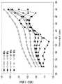
図2aは、理想的な場合と実在的な場合のキャリア増幅器106及びピーキング増幅器108の基本電流成分を示したグラフである。
FIG. 2a is a graph showing the basic current components of the
図2aを参照すると、理想的な場合キャリア増幅器106及びピーキング増幅器108の基本電流成分は、入力電圧の増加によって一定な傾きを有することをよく見られる。しかし、実在的な場合において、キャリア増幅器106とピーキング増幅器108は半導体素子であるFET(Field Effect Transistor)、HEMT(High Electron Mobility Transistor)、あるいはBJT(Bipolar Junction Transistor)などで構成されることができるし、前記FET、HEMT、あるいはBJTの場合電流成分は、入力電圧によって二乗形態や指数形態で増加されるようになる。前記電流特性をピーキング増幅器108に適用をするようになったらピーキング増幅器108の基本電流成分は、図2aの実在的な電流特性のようである。
Referring to FIG. 2a, it is often seen that the fundamental current components of the
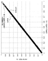
図2bは理想的な場合と実在的な場合のキャリア増幅器106及びピーキング増幅器108の基本電圧成分を示したグラフである。
FIG. 2b is a graph showing the basic voltage components of the
図2bを参照すると理想的な場合と実在的な場合のキャリア増幅器106及びピーキング増幅器108の基本電圧成分は、同一であることを確認することができる。これは、基本電圧成分は基本電流成分とキャリア増幅器106及びピーキング増幅器108の出力整合インピーダンスで決定されるが、出力整合インピーダンスは次式に従う。
Referring to FIG. 2b, it can be confirmed that the fundamental voltage components of the

ここで、vinは入力電圧であり、Zcはキャリア増幅器106の出力整合インピーダンスであり、Zpはピーキング増幅器108の出力整合インピーダンスであり、ZLはキャリア増幅器106とピーキング増幅器108の電力が結合される支点での整合インピーダンスであり、ZTは結合器114内のキャリア増幅器106とピーキング増幅器108の間のクォータウエーブ伝送ラインの特性インピーダンスを示す。一般に、ZLはZT/2の関係を有する。また、Icはキャリア増幅器106の入力電流であり、Ipはピーキング増幅器108の入力電流である。
Here, vin is an input voltage, Zc is an output matching impedance of the
前記式を参照すると、たとえ実在的な場合ピーキング増幅器108の基本電流成分が理想的な場合より小さいが、Zc及びZpの大きさが増加されるので、前記図2bのように理想的な場合と実在的な場合の基本電圧成分が同一であることを確認することができる。
Referring to the above equation, even if the fundamental current component of the peaking
図3は、理想的な場合と実在的な場合のドハティ増幅器100の入出力電力を示したグラフである。
FIG. 3 is a graph showing input / output power of the Doherty
図3を参照すると、理想的な場合ドハティ増幅器100は、線形的な入出力電力関係を有する。しかし、実在的な場合ドハティ増幅器100は、前記図2aに示したところのようにピーキング増幅器108の基本電流成分が減るために、理想的な場合の出力電力大きさより低い出力電力を有するようになるので、結合されたドハティ増幅器100の出力電力は、線形的な関係を有することができなくなって、したがって、望まない歪曲特性を有するようになる。
Referring to FIG. 3, in the ideal case, the Doherty
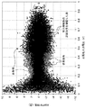
図4は、実在的なドハティ増幅器のメモリー効果(Memory Effect)を示したグラフである。 FIG. 4 is a graph showing a memory effect of a real Doherty amplifier.
前記メモリー効果は、増幅器の歪曲成分が現在の入力信号だけではなく、過去の入力信号によって影響を受けるようになることを意味する。増幅器のメモリー効果は、ツートン(Two−tone)信号を利用した非線形性測定を通じて調べることができる。増幅器にツートン信号を印加して、同じ出力電力で増幅器の基本波成分と3次歪曲信号をよく見れば、ツートン信号の帯域幅によってお互いに異なる大きさと位相を有する3次歪曲信号をよく見られるが、このような方法を通じてメモリー効果を測定することができる。一般に、メモリー効果は、中間出力電力大きさでたくさん発生して、低い出力電力では増幅器自体で発生させる歪曲成分が小さくて、メモリー効果が多く現われない。そして、高い出力電力大きさでは電力増幅器自体で発生させる歪曲成分が多くてメモリー効果を認知することができない。 The memory effect means that the distortion component of the amplifier becomes affected not only by the current input signal but also by past input signals. The memory effect of the amplifier can be examined through non-linearity measurement using a two-tone signal. If a two-tone signal is applied to the amplifier and the fundamental component of the amplifier and the third-order distorted signal are observed with the same output power, a third-order distorted signal having a different magnitude and phase depending on the bandwidth of the two-tone signal can be often seen. However, the memory effect can be measured through such a method. In general, a large amount of memory effect is generated at the intermediate output power, and at low output power, the distortion component generated by the amplifier itself is small, and the memory effect does not appear much. When the output power is high, there are many distortion components generated by the power amplifier itself, and the memory effect cannot be recognized.
前記図4を参照すると、ドハティ増幅器は、一般的な増幅器とメモリー効果特性を示すことをよく見られる。これは、前記ドハティ増幅器はキャリア増幅器とピーキング増幅器で構成されて、前記キャリア増幅器とピーキング増幅器はお互いに異なる動作をするために、お互いに異なる歪曲特性を示すためである。 Referring to FIG. 4, it is often seen that the Doherty amplifier exhibits a memory effect characteristic with a general amplifier. This is because the Doherty amplifier includes a carrier amplifier and a peaking amplifier, and the carrier amplifier and the peaking amplifier operate differently from each other, and thus exhibit different distortion characteristics.
前記したところのように、ドハティ増幅器だけではなく、他の電力増幅器は非線形成分を発生させて、出力信号を歪曲させるために信号の品質を落とすようになる。よって、通信システムの線形性要求事項のためには別途の線形化技術が必要になる。線形化技術のうちで、デジタル前置歪曲器は信号をデジタル帯域で処理することで、他の線形化技術に比べて経済性及び拡張可能性が卓越である。 As described above, not only the Doherty amplifier but also other power amplifiers generate non-linear components and degrade the signal quality in order to distort the output signal. Therefore, a separate linearization technique is required for the linearity requirement of the communication system. Among the linearization techniques, the digital predistorter processes signals in the digital band, and thus has excellent economics and expandability compared to other linearization techniques.
図5は、本発明が適用されるデジタル前置歪曲器を含んだドハティ増幅システムの構成図である。 FIG. 5 is a block diagram of a Doherty amplification system including a digital predistorter to which the present invention is applied.
図5を参照すると、ドハティ増幅システムはドハティ増幅器100と、デジタル前置歪曲器200と、デジタル前置歪曲器制御器300とDAC(Digital−Analog Converter)400とADC(Analog−Digital Converter)500とアップコンバータ600とダウンコンバータ700を含む。
Referring to FIG. 5, the Doherty amplification system includes a Doherty
図5に示したドハティ増幅システムの動作を説明すると次のようである。 The operation of the Doherty amplification system shown in FIG. 5 will be described as follows.
デジタル前置歪曲器200は、最初動作時に初期モードに入って行く。
The
初期モードとは、ドハティ増幅器100の非線形特性及びメモリー効果を測定する動作モードであり、初期モードではドハティ増幅器100の全体動作領域での特性が分かることができる特定の信号を使用するか、または実際通信システムの信号を一定時間の間に使用することができる。前記初期モードで使用する信号を通称して試験信号であると称する。
The initial mode is an operation mode for measuring the non-linear characteristic and memory effect of the Doherty
まず、試験信号としてデジタル信号がデジタル前置歪曲器200とデジタル前置歪曲器制御器300に入力される。しかし、初期モードでデジタル前置歪曲器200に入力された信号は、何らの前置歪曲を受けないで通過するようになる。デジタル前置歪曲器200を通過した信号は、DAC400を経ってアナログ信号に変換される。DAC400を経ったアナログ信号は、アップコンバータ600に入力されて高い周波数のアナログ信号に変換されながら、これはドハティ増幅器100に入力されて増幅される。ドハティ増幅器100によって増幅されたアナログ信号は歪曲されて非線形特性及びメモリー効果を有するようになる。ドハティ増幅器100によって増幅された大部分の信号は、空中に伝えて一部は、ダウンコンバータ700によって低い周波数の信号に変換される。ダウンコンバータ700を経った低い周波数のアナログ信号は、ADC500を通じてデジタル信号に変換される。ADC500を経ったデジタル信号は、デジタル前置歪曲器制御器300に入力される。
First, a digital signal is input to the
デジタル前置歪曲器制御器300では、前記試験信号と前記ドハティ増幅器100によって歪曲された信号を比べて、前記ドハティ増幅器100によって発生された非線形特性とメモリー効果を感知する。前記デジタル前置歪曲器制御器300は、これを利用して前記ドハティ増幅器100の非線形特性及びメモリー効果を補償するためにデジタル前置歪曲器200の構成値を計算するようになる。
The
参照で、本特許で説明の容易のために、非線形特性は入力される信号の大きさに比例して出力信号の大きさが非線形的に変わる特性(AM−to−AM;Amplitude Modulation−to−Amplitude Modulation)と出力信号の位相が非線形的に変わる特性(AM−to−PM;Amplitude Modulation−to−Phase Modulation)を示す。デジタル前置歪曲器200は、ルックアップテーブル(LUT;Look−up Table)や多項式などでなされる。
For ease of explanation in this patent, the non-linear characteristic is a characteristic in which the magnitude of the output signal varies non-linearly in proportion to the magnitude of the input signal (AM-to-AM; Amplitude Modulation-to-). Amplitude Modulation) and a characteristic (AM-to-PM; Amplitude Modulation-to-Phase Modulation) in which the phase of the output signal changes nonlinearly. The
したがって、デジタル前置歪曲制御器300は、デジタル前置歪曲器200のLUT構成値を提供するか、または多項式の係数を提供する。
Accordingly, the
図6は、従来技術によるデジタル前置歪曲器200の内部構成図を示す。
FIG. 6 shows an internal configuration diagram of a
図6を参照すると、従来技術によるデジタル前置歪曲器は、増幅器補償器210で構成される。
Referring to FIG. 6, the digital predistorter according to the prior art includes an
前記増幅器補償器210は、ドハティ増幅器100の非線形特性のみを補償するか、または非線形特性だけではなく、メモリー効果を補償する。また、前記増幅器補償器210を通過した信号は、図5のDAC400の入力になる。
The
前記増幅器補償器210は、多項式で構成されるか、またはLUTで構成されるか、または多項式とLUTとで構成されることができる。また、前記増幅器補償器210は、ボルテラシリーズ(Volterra Series)、ボルテラシリーズ(Volterra Series)の縮小モデル、ウィーナー(Wiener)モデル、ウィーナー(Wiener)モデルの拡張モデル、ハンマースタイン(Hammerstein)モデル、ハンマースタイン(Hammerstein)の拡張モデルなどが適用されることができる。
The
一般に、線形化される複数個の歪曲発生源を有する増幅器がそれぞれの歪曲発生源から出力される非線形特性及びメモリー効果が同じであったら、前記図6の増幅器補償器210を通じて非線形特性及びメモリー効果を充分に補償することができる。
In general, if the amplifier having a plurality of distortion sources to be linearized has the same nonlinear characteristic and memory effect output from the respective distortion sources, the nonlinear characteristic and the memory effect can be obtained through the
しかし、ドハティ増幅器のようにお互いに相異な非線形特性及びメモリー効果を有する歪曲発生源で構成された増幅器なら、前記増幅器補償器210のように従来方式の線形化方式に従って線形化するにおいて、線形化改善程度に制約が発生するようになる。
However, if the amplifier is composed of distortion sources having different nonlinear characteristics and memory effects such as Doherty amplifier, linearization is performed in the linearization according to the conventional linearization method such as the
前述したところのような問題点を解決するために、本発明の目的は、複数個の歪曲発生源を有する増幅器を効果的に線形化する方法及び装置を提供することにある。 In order to solve the problems as described above, it is an object of the present invention to provide a method and apparatus for effectively linearizing an amplifier having a plurality of distortion sources.
本発明で提案する装置は、複数個の歪曲発生源を有する増幅器を効果的に線形化する装置において、それぞれの歪曲発生源の歪曲特性を補償するための複数個のデジタル前置歪曲補償器と、入力信号の大きさによって複数個のデジタル前置歪曲器のうちで一つの経路を選択してくれる信号分離部と、複数個のデジタル前置歪曲器を通過した前置歪曲された信号を結合してくれる信号結合器を含んで、前記信号分離部の経路選択は、歪曲された信号の非線形特性及びメモリー効果によって決めることを特徴とする。 The apparatus proposed in the present invention is an apparatus for effectively linearizing an amplifier having a plurality of distortion sources, and a plurality of digital predistorters for compensating for the distortion characteristics of the respective distortion sources; Combines a signal separator that selects one path among multiple digital predistorters according to the magnitude of the input signal and a predistorted signal that has passed through multiple digital predistorters The signal selection unit includes a signal combiner, and the path selection is determined by the non-linear characteristic of the distorted signal and the memory effect.
本発明で提案する方法は、複数個の歪曲発生源を有する増幅器を効果的に線形化する方法において、それぞれの歪曲発生源の歪曲特性を補償するための複数個のデジタル前置歪曲補償方法を通じて前置歪曲信号を生成する過程と、入力信号の大きさによって複数個のデジタル前置歪曲器のうちで一つの経路を選択してくれる過程と、複数個のデジタル前置歪曲器を通過した前置歪曲された信号を結合してくれる過程を含んで、前記信号分離過程において経路選択は、歪曲された信号の非線形特性及びメモリー効果によって決めることを特徴とする。 The method proposed in the present invention is a method of effectively linearizing an amplifier having a plurality of distortion sources through a plurality of digital predistortion compensation methods for compensating for the distortion characteristics of each distortion source. The process of generating a predistortion signal, the process of selecting one path among a plurality of digital predistorters according to the magnitude of the input signal, and the state before passing through a plurality of digital predistorters The path selection in the signal separation process is determined by the nonlinear characteristics of the distorted signal and the memory effect, including a process of combining the distorted signals.
本発明で提案される線形化装置は、複数個の歪曲発生源で発生する相異な非線形特性及びメモリー効果を補償するために、それぞれの歪曲発生源の歪曲特性を補償するための複数個のデジタル前置歪曲器を提供することで、前記複数個の歪曲発生源で発生される歪曲信号を効果的に補償することができる。 The linearization apparatus proposed in the present invention includes a plurality of digital units for compensating for distortion characteristics of respective distortion sources in order to compensate for different nonlinear characteristics and memory effects generated at a plurality of distortion sources. By providing a predistorter, it is possible to effectively compensate for distortion signals generated by the plurality of distortion sources.
以下、本発明に添付された図面を参照して本発明の望ましい実施例を詳しく説明する。まず、図面のうちで、同一な構成要素または部品はできるだけ同一な参照符号を示していることに留意しなければならない。本発明を説明するにおいて、係わる公知機能あるいは構成に対する具体的な説明が本発明の要旨を曇らせることがあると判断される場合にはその詳細な説明を略する。 Hereinafter, exemplary embodiments of the present invention will be described in detail with reference to the accompanying drawings. First, it should be noted that in the drawings, the same components or parts have the same reference numerals as much as possible. In the description of the present invention, if it is determined that a specific description of a related known function or configuration may cloud the gist of the present invention, a detailed description thereof will be omitted.
本発明の詳細な説明の前で本発明のデジタル前置歪曲器は、複数個の増幅器を通じて増幅をする時、複数個の歪曲発生源から発生する相異な非線形特性及びメモリー効果を補償する時適用可能な発明で、下でドハティ増幅器をその例で説明しようとする。 Prior to the detailed description of the present invention, the digital predistorter of the present invention is applied when amplifying through a plurality of amplifiers to compensate for different nonlinear characteristics and memory effects generated from a plurality of distortion sources. In a possible invention, the Doherty amplifier will be described below by way of example.
図7aは本発明の第1実施例によるデジタル前置歪曲器の内部構成図である。 FIG. 7a is an internal block diagram of the digital predistorter according to the first embodiment of the present invention.
図7aを参照すると、前記デジタル前置歪曲器は、信号分離部220と、第1増幅器補償器222と、第2増幅器補償器224と、信号結合部226を含む。
Referring to FIG. 7 a, the digital predistorter includes a
前記信号分離部220は、入力信号の大きさを一定臨界値と比べて、第1増幅器補償器222、あるいは第2増幅器補償器224に出力する。すなわち、入力信号の大きさを0から1までであると思ったら、入力信号が0から前記臨界値までは前記信号分離部220は入力信号を前記第1増幅器補償器222に出力して、入力信号が前記臨界値から1までは前記信号分離部220は入力信号を前記第2増幅器補償器224に出力する。ドハティ増幅器を例に挙げようとすると、第1増幅器はキャリア増幅器であり、第2増幅器はピーキング増幅器である。前記臨界値は、前記ピーキング増幅器が理想的に動作される場合に動作を始める時点に相応する入力信号の大きさで設定される。
The
前記第1増幅器補償器222及び前記第2増幅器補償器224は、前記信号分離部220から入力を受けた信号を利用して、増幅器の歪曲成分を補償するための逆歪曲信号を出力する。この時、前記第1増幅器補償器222及び前記第2増幅器補償器224は、増幅器の非線形特性だけではなく、メモリー効果を補償するための逆歪曲信号を補償するための補償値を前記図5のデジタル前置歪曲器制御器300を通じて獲得した状態である。
The
前記第1増幅器補償器222及び前記第2増幅器補償器224は、多項式で構成されるか、またはLUTで構成されるか、または多項式とLUTで構成されることができる。また、前記増幅器補償器210は、ボルテラシリーズ(Volterra Series)、ボルテラシリーズ(Volterra Series)の縮小モデル、ウィーナー(Wiener)モデル、ウィーナー(Wiener)モデルの拡張モデル、ハンマースタイン(Hammerstein)モデル、ハンマースタイン(Hammerstein)の拡張モデルなどが適用されることができる。これだけではなく、前記第1増幅器補償器222及び前記第2増幅器補償器224は、増幅器の非線形特性及びメモリー効果を補償することができる能力を有した場合ならどのような形態でも本発明の補償器に適用することができることは当業者に自明であると言える。
The
前記信号結合部226は、前記第1増幅器補償器222及び前記第2増幅器補償器224から出力された逆歪曲信号の入力を受けて図5のDAC400の入力で使用される出力信号を出す。
The
前述したところのように、複数個の歪曲発生源を有する増幅器で、信号の大きさによって歪曲発生信号の寄与度が大きい発生源に合うように補償器を利用することで、効果的に歪曲発生源で発生する歪曲信号を償ってくれることができる。 As described above, an amplifier having a plurality of distortion generation sources can effectively generate distortion by using a compensator so that the contribution of the distortion generation signal is large depending on the signal size. It can compensate for the distortion signal generated at the source.
図7bは、本発明の第2実施例によるデジタル前置歪曲器の内部構成図である。 FIG. 7b is an internal block diagram of a digital predistorter according to the second embodiment of the present invention.
図7bを参照すると、前記デジタル前置歪曲器は信号分離部220と、第1増幅器補償器222と、第2増幅器補償器224と、信号結合部226と、増幅器補償器228を含む。
Referring to FIG. 7 b, the digital predistorter includes a
前記信号分離部220、前記第1増幅器補償器222、前記第2増幅器補償器224及び前記信号結合部226は図7aでの動作と同一であるので、その詳細な説明は略することにする。
Since the
前記増幅器補償器228は、前記信号結合部226から出力された第1増幅器補償器222及び第2増幅器補償器224を通じて作られた逆歪曲信号の入力を受けて追加的な増幅器補償信号を出力する。
The
前記増幅器補償器228は、複数個の歪曲発生源で発生された歪曲信号の間の干渉、あるいは臨界値によって発生された逆歪曲信号の間の不連続性などを追加的に補償する。
The
前記増幅器補償器228は、前記第1増幅器補償器222及び前記第2増幅器補償器224と同じく、増幅器の非線形特性及びメモリー効果を補償することができる能力を有した場合ならどのような形態でも本発明の補償器に適用することができることは当業者に自明であると言える。
As with the
また、前記増幅器補償器228は、前記信号結合器220の後に配置されることもできるが、前記信号分離器220前に配置されることもでき、その機能は上述したところのようである。図7cは上のような構成を示す。
The
図8aは、本発明によるモデリングされたAM/AM特性を示したグラフである。図8bは本発明によるモデリングされたAM/PM特性を示したグラフである。 FIG. 8a is a graph illustrating the AM / AM characteristics modeled according to the present invention. FIG. 8b is a graph showing the modeled AM / PM characteristics according to the present invention.
図8aと8bを参照すると、本発明によるモデリング性能が従来技術によるモデリング性能に比べて、増幅器出力に対してさらに優秀な特性を示すことをよく見られる。 Referring to FIGS. 8a and 8b, it is often seen that the modeling performance according to the present invention exhibits even better characteristics for the amplifier output compared to the modeling performance according to the prior art.
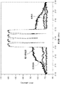
図9aは、本発明による電力増幅器線形化後のスペクトラムを示したグラフである。図9bは、本発明による電力増幅器線形化後のAM/AM特性を示したグラフである。図9cは、本発明による電力増幅器線形化後のAM/PM特性を示したグラフである。 FIG. 9a is a graph showing the spectrum after linearization of the power amplifier according to the present invention. FIG. 9b is a graph illustrating AM / AM characteristics after power amplifier linearization according to the present invention. FIG. 9c is a graph showing AM / PM characteristics after linearization of the power amplifier according to the present invention.
図9aないし図9cを参照すると、本発明による線形化性能が従来技術による線形化性能に比べて増幅器出力に対してさらに優秀な特性を示すことをよく見られる。 Referring to FIGS. 9a through 9c, it is often seen that the linearization performance according to the present invention exhibits even better characteristics for the amplifier output compared to the linearization performance according to the prior art.
前述したところのように、複数個の歪曲発生源を有する増幅器の歪曲特性を補償するために、複数個の補償器を利用することで、優秀なモデリング特性を示すことができるし、これによって優秀な線形化結果が出力されることをよく見られる。 As described above, by using multiple compensators to compensate for the distortion characteristics of an amplifier having multiple distortion sources, excellent modeling characteristics can be exhibited. It is often seen that a linearization result is output.
今まで本発明の実施例に局限して説明したが、本発明の技術が当業者によって容易に変形実施される可能性は自明である。このような変形される実施例は、本発明の特許請求範囲に記載した技術思想に当然含まれるものとして解釈されなければならないであろう。 Although the present invention has been limited to the embodiments of the present invention, it is obvious that the technology of the present invention can be easily modified by those skilled in the art. Such modified embodiments should be construed as naturally included in the technical idea described in the claims of the present invention.
本発明で提案される線形化装置は、複数個の歪曲発生源で発生する相異な非線形特性及びメモリー効果を補償するために、それぞれの歪曲発生源の歪曲特性を補償するための複数個のデジタル前置歪曲器を提供することで、前記複数個の歪曲発生源で発生される歪曲信号を効果的に補償することができる。 The linearization apparatus proposed in the present invention includes a plurality of digital units for compensating for distortion characteristics of respective distortion sources in order to compensate for different nonlinear characteristics and memory effects generated at a plurality of distortion sources. By providing a predistorter, it is possible to effectively compensate for distortion signals generated by the plurality of distortion sources.
100…ドハティ増幅器、
102…電力分配器、
104…入力位相補償部、
106…キャリア増幅器、
108…ピーキング増幅器、
110、112…オフセットライン、
114…結合器、
200…デジタル前置歪曲器、
220…信号分離部、
222…第1増幅器補償器、
224…第2増幅器補償器、
226…信号結合部、
228…増幅器補償器、
300…デジタル前置歪曲器制御器、
400…DAC、
500…ADC、
600…アップコンバータ、
700…ダウンコンバータ。
100 ... Doherty amplifier,
102: Power distributor,
104: Input phase compensation unit,
106: Carrier amplifier,
108: Peaking amplifier,
110, 112 ... offset line,
114: coupler,
200: Digital predistorter,
220: Signal separation unit,
222: first amplifier compensator;
224 ... second amplifier compensator,
226 ... Signal coupling unit,
228 ... Amplifier compensator,
300 ... Digital predistorter controller,
400 ... DAC,
500 ... ADC,
600 ... Upconverter,
700: Down converter.
Claims (20)
入力信号の大きさによって信号の経路を選択してくれる信号分離部と、
複数個の補償器と、及び
複数個の補償器の出力信号を結合する信号結合部を含んで、
前記信号分離部は、前記入力信号の大きさと臨界値との大きさの比較を通じて前記複数個の補償器のうちで一つの補償器に出力することを特徴とする線形化装置。 In an apparatus for linearizing an amplifier having a plurality of distortion sources,
A signal separation unit that selects a signal path according to the size of the input signal;
Including a plurality of compensators and a signal combining unit for combining the output signals of the plurality of compensators;
The linearization apparatus, wherein the signal separation unit outputs the signal to one compensator among the plurality of compensators through a comparison between a magnitude of the input signal and a critical value.
入力信号の大きさによって信号の経路を選択してくれる信号分離過程と、
複数個の補償信号を生成する過程と、
複数個の補償信号を結合する過程を含んで、
前記信号分離過程は、前記入力信号の大きさと臨界値との大きさの比較を通じて前記複数個の補償信号を生成する過程のうちで一つの補償信号生成過程で出力することを特徴とする線形化方法。 In a method for linearizing an amplifier having a plurality of distortion sources,
A signal separation process that selects the signal path according to the size of the input signal,
Generating a plurality of compensation signals;
Including the step of combining a plurality of compensation signals,
The linearization characterized in that the signal separation process outputs the compensation signal in one of the plurality of compensation signal generation processes by comparing the magnitude of the input signal with a critical value. Method.
Applications Claiming Priority (2)
| Application Number | Priority Date | Filing Date | Title |
|---|---|---|---|
| KR10-2010-0099301 | 2010-10-12 | ||
| KR1020100099301A KR101128487B1 (en) | 2010-10-12 | 2010-10-12 | Power amplifier linearization method and apparatus |
Publications (1)
| Publication Number | Publication Date |
|---|---|
| JP2012085295A true JP2012085295A (en) | 2012-04-26 |
Family
ID=44759601
Family Applications (1)
| Application Number | Title | Priority Date | Filing Date |
|---|---|---|---|
| JP2011224124A Pending JP2012085295A (en) | 2010-10-12 | 2011-10-11 | Power amplifier linearization method and apparatus |
Country Status (5)
| Country | Link |
|---|---|
| US (1) | US8587375B2 (en) |
| EP (1) | EP2442441B1 (en) |
| JP (1) | JP2012085295A (en) |
| KR (1) | KR101128487B1 (en) |
| CN (1) | CN102447442A (en) |
Cited By (2)
| Publication number | Priority date | Publication date | Assignee | Title |
|---|---|---|---|---|
| JP2012178821A (en) * | 2011-02-24 | 2012-09-13 | Pohang Univ Of Science & Technology Academy-Industry Cooperation | THREE-STAGE GALLIUM NITRIDE HIGH ELECTRON MOBILITY TRANSISTOR (GaN HEMT) DOHERTY POWER AMPLIFIER FOR HIGH FREQUENCY APPLICATION |
| JP2016504903A (en) * | 2012-12-18 | 2016-02-12 | ヌクレウス サイエンティフィック, インク.Nucleus Scientific, Inc. | Nonlinear system identification for wireless power transfer optimization |
Families Citing this family (11)
| Publication number | Priority date | Publication date | Assignee | Title |
|---|---|---|---|---|
| US10387592B1 (en) | 2010-05-26 | 2019-08-20 | Keysight Technologies, Inc. | Method and system for characterizing, modeling and simulating non-linear components having long term memory effects |
| US8880014B2 (en) | 2010-06-07 | 2014-11-04 | Skyworks Solutions, Inc. | CMOS RF switch device and method for biasing the same |
| US8914271B2 (en) * | 2011-11-30 | 2014-12-16 | Keysight Technologies, Inc. | Method for predistorting signals for non-linear components in the presence of long term memory effects |
| WO2014205725A1 (en) * | 2013-06-27 | 2014-12-31 | 华为技术有限公司 | Multiband power amplifier device |
| US20150160279A1 (en) * | 2013-12-09 | 2015-06-11 | Qualcomm Incorporated | Quantitative characterization of nonlinearity and memory effect in nonlinear circuits |
| CN103746658A (en) * | 2013-12-17 | 2014-04-23 | 福建星网锐捷网络有限公司 | Power amplification device for power amplification of signals output by AP and AP device |
| WO2015192320A1 (en) * | 2014-06-17 | 2015-12-23 | 华为技术有限公司 | Radio frequency power amplification system, radio frequency power amplification method, transmitter, and base station |
| US10985951B2 (en) | 2019-03-15 | 2021-04-20 | The Research Foundation for the State University | Integrating Volterra series model and deep neural networks to equalize nonlinear power amplifiers |
| GB2592678A (en) * | 2020-03-06 | 2021-09-08 | Sony Semiconductor Solutions Corp | Amplifier and amplification method |
| CN113708731B (en) * | 2021-08-25 | 2022-07-29 | 优镓科技(北京)有限公司 | Linearity enhanced Doherty power amplifier based on phase mismatch |
| CN114553153A (en) * | 2022-02-28 | 2022-05-27 | 电子科技大学 | Amplitude-phase independent adjustable analog predistortion linearizer |
Citations (2)
| Publication number | Priority date | Publication date | Assignee | Title |
|---|---|---|---|---|
| JP2003092518A (en) * | 2001-09-18 | 2003-03-28 | Hitachi Kokusai Electric Inc | Distortion compensator |
| JP2006165856A (en) * | 2004-12-06 | 2006-06-22 | Hitachi Kokusai Electric Inc | Amplifying device |
Family Cites Families (8)
| Publication number | Priority date | Publication date | Assignee | Title |
|---|---|---|---|---|
| US20060083330A1 (en) * | 2002-12-17 | 2006-04-20 | Matsushita Electric Industrial Co., Ltd. | Distortion compensation table creation method and distortion compensation method |
| KR100518456B1 (en) * | 2003-10-10 | 2005-09-30 | 학교법인 포항공과대학교 | Digital feedback linearizer for linearizing power amplifier and method therefor |
| EP1758242A4 (en) * | 2004-06-18 | 2008-04-09 | Mitsubishi Electric Corp | High-efficiency amplifier |
| US20080111622A1 (en) * | 2006-11-14 | 2008-05-15 | Roland Sperlich | Hybrid Doherty Amplifier System and Method |
| EP2132872B1 (en) * | 2007-03-30 | 2018-11-28 | Apple Inc. | Amplifier pre-distortion systems and methods |
| JP5022792B2 (en) * | 2007-07-02 | 2012-09-12 | 株式会社日立国際電気 | DCDC converter unit, power amplifier, and base station apparatus |
| US7889811B2 (en) * | 2007-09-06 | 2011-02-15 | Samsung Electro-Mechanics | Digital linear amplification with nonlinear components (LINC) transmitter |
| US7619468B1 (en) * | 2008-09-30 | 2009-11-17 | Nortel Networks Limited | Doherty amplifier with drain bias supply modulation |
-
2010
- 2010-10-12 KR KR1020100099301A patent/KR101128487B1/en not_active IP Right Cessation
-
2011
- 2011-10-11 EP EP11184702.6A patent/EP2442441B1/en not_active Not-in-force
- 2011-10-11 US US13/270,552 patent/US8587375B2/en active Active
- 2011-10-11 JP JP2011224124A patent/JP2012085295A/en active Pending
- 2011-10-12 CN CN2011103079153A patent/CN102447442A/en active Pending
Patent Citations (2)
| Publication number | Priority date | Publication date | Assignee | Title |
|---|---|---|---|---|
| JP2003092518A (en) * | 2001-09-18 | 2003-03-28 | Hitachi Kokusai Electric Inc | Distortion compensator |
| JP2006165856A (en) * | 2004-12-06 | 2006-06-22 | Hitachi Kokusai Electric Inc | Amplifying device |
Cited By (2)
| Publication number | Priority date | Publication date | Assignee | Title |
|---|---|---|---|---|
| JP2012178821A (en) * | 2011-02-24 | 2012-09-13 | Pohang Univ Of Science & Technology Academy-Industry Cooperation | THREE-STAGE GALLIUM NITRIDE HIGH ELECTRON MOBILITY TRANSISTOR (GaN HEMT) DOHERTY POWER AMPLIFIER FOR HIGH FREQUENCY APPLICATION |
| JP2016504903A (en) * | 2012-12-18 | 2016-02-12 | ヌクレウス サイエンティフィック, インク.Nucleus Scientific, Inc. | Nonlinear system identification for wireless power transfer optimization |
Also Published As
| Publication number | Publication date |
|---|---|
| KR101128487B1 (en) | 2012-06-21 |
| US20120086507A1 (en) | 2012-04-12 |
| EP2442441A3 (en) | 2012-05-30 |
| CN102447442A (en) | 2012-05-09 |
| EP2442441A2 (en) | 2012-04-18 |
| US8587375B2 (en) | 2013-11-19 |
| EP2442441B1 (en) | 2014-07-09 |
Similar Documents
| Publication | Publication Date | Title |
|---|---|---|
| KR101128487B1 (en) | Power amplifier linearization method and apparatus | |
| JP4679021B2 (en) | Method and apparatus for generating radio frequency signals | |
| JP5591106B2 (en) | Digital hybrid mode power amplifier system | |
| US8736365B2 (en) | Broadband linearization module and method | |
| US20140327481A1 (en) | Digital hybrid mode power amplifier system | |
| JP5603785B2 (en) | Amplifier | |
| US20120294387A1 (en) | Extended bandwidth digital doherty transmitter | |
| JP5907073B2 (en) | Amplifier circuit and wireless communication device | |
| JP5049562B2 (en) | Power amplifier | |
| SE541265C2 (en) | Extended bandwidth digital doherty transmitter | |
| KR20170054283A (en) | Analog rf pre-distorter and non-linear splitter | |
| EP2277262B1 (en) | Feedforward linearization of rf power amplifiers | |
| US20050088230A1 (en) | Amplifier pre-distortion processing based on composite look-up tables | |
| KR101128485B1 (en) | Envelope tracking power amplifing apparatus using sweet spot tracking | |
| Lee et al. | A wideband analog predistortion power amplifier with multi-branch nonlinear path for memory-effect compensation | |
| KR101358096B1 (en) | Power amplifier | |
| KR100865886B1 (en) | Apparatus for calibrating non-linearity of amplifier | |
| JP2015099972A (en) | Transmitter module | |
| JP5795218B2 (en) | ET power amplifier | |
| Mohammady et al. | Efficiency improvement in microwave power amplifiers by using Complex Gain Predistortion technique | |
| US6867648B2 (en) | Linearization apparatus capable of adjusting peak-to-average power ratio | |
| Lee et al. | A transistor-based analog predistorter with unequal delays for memory compensation | |
| KR20130119089A (en) | Doherty amplify apparatus and method | |
| Breed et al. | An overview of common techniques for power amplifier linearization | |
| KR20070081199A (en) | Apparatus for compensating memory effect of power amplifier in a wireless communication system |
Legal Events
| Date | Code | Title | Description |
|---|---|---|---|
| A977 | Report on retrieval |
Free format text: JAPANESE INTERMEDIATE CODE: A971007 Effective date: 20120903 |
|
| A131 | Notification of reasons for refusal |
Free format text: JAPANESE INTERMEDIATE CODE: A131 Effective date: 20120911 |
|
| A601 | Written request for extension of time |
Free format text: JAPANESE INTERMEDIATE CODE: A601 Effective date: 20121210 |
|
| A602 | Written permission of extension of time |
Free format text: JAPANESE INTERMEDIATE CODE: A602 Effective date: 20121213 |
|
| A02 | Decision of refusal |
Free format text: JAPANESE INTERMEDIATE CODE: A02 Effective date: 20130305 |