JP2012058274A - Display device - Google Patents
Display device Download PDFInfo
- Publication number
- JP2012058274A JP2012058274A JP2010198307A JP2010198307A JP2012058274A JP 2012058274 A JP2012058274 A JP 2012058274A JP 2010198307 A JP2010198307 A JP 2010198307A JP 2010198307 A JP2010198307 A JP 2010198307A JP 2012058274 A JP2012058274 A JP 2012058274A
- Authority
- JP
- Japan
- Prior art keywords
- voltage
- display device
- display
- gate
- light emission
- Prior art date
- Legal status (The legal status is an assumption and is not a legal conclusion. Google has not performed a legal analysis and makes no representation as to the accuracy of the status listed.)
- Pending
Links
Images


Classifications
-
- G—PHYSICS
- G09—EDUCATION; CRYPTOGRAPHY; DISPLAY; ADVERTISING; SEALS
- G09G—ARRANGEMENTS OR CIRCUITS FOR CONTROL OF INDICATING DEVICES USING STATIC MEANS TO PRESENT VARIABLE INFORMATION
- G09G3/00—Control arrangements or circuits, of interest only in connection with visual indicators other than cathode-ray tubes
- G09G3/20—Control arrangements or circuits, of interest only in connection with visual indicators other than cathode-ray tubes for presentation of an assembly of a number of characters, e.g. a page, by composing the assembly by combination of individual elements arranged in a matrix no fixed position being assigned to or needed to be assigned to the individual characters or partial characters
- G09G3/22—Control arrangements or circuits, of interest only in connection with visual indicators other than cathode-ray tubes for presentation of an assembly of a number of characters, e.g. a page, by composing the assembly by combination of individual elements arranged in a matrix no fixed position being assigned to or needed to be assigned to the individual characters or partial characters using controlled light sources
- G09G3/30—Control arrangements or circuits, of interest only in connection with visual indicators other than cathode-ray tubes for presentation of an assembly of a number of characters, e.g. a page, by composing the assembly by combination of individual elements arranged in a matrix no fixed position being assigned to or needed to be assigned to the individual characters or partial characters using controlled light sources using electroluminescent panels
- G09G3/32—Control arrangements or circuits, of interest only in connection with visual indicators other than cathode-ray tubes for presentation of an assembly of a number of characters, e.g. a page, by composing the assembly by combination of individual elements arranged in a matrix no fixed position being assigned to or needed to be assigned to the individual characters or partial characters using controlled light sources using electroluminescent panels semiconductive, e.g. using light-emitting diodes [LED]
- G09G3/3208—Control arrangements or circuits, of interest only in connection with visual indicators other than cathode-ray tubes for presentation of an assembly of a number of characters, e.g. a page, by composing the assembly by combination of individual elements arranged in a matrix no fixed position being assigned to or needed to be assigned to the individual characters or partial characters using controlled light sources using electroluminescent panels semiconductive, e.g. using light-emitting diodes [LED] organic, e.g. using organic light-emitting diodes [OLED]
- G09G3/3225—Control arrangements or circuits, of interest only in connection with visual indicators other than cathode-ray tubes for presentation of an assembly of a number of characters, e.g. a page, by composing the assembly by combination of individual elements arranged in a matrix no fixed position being assigned to or needed to be assigned to the individual characters or partial characters using controlled light sources using electroluminescent panels semiconductive, e.g. using light-emitting diodes [LED] organic, e.g. using organic light-emitting diodes [OLED] using an active matrix
- G09G3/3233—Control arrangements or circuits, of interest only in connection with visual indicators other than cathode-ray tubes for presentation of an assembly of a number of characters, e.g. a page, by composing the assembly by combination of individual elements arranged in a matrix no fixed position being assigned to or needed to be assigned to the individual characters or partial characters using controlled light sources using electroluminescent panels semiconductive, e.g. using light-emitting diodes [LED] organic, e.g. using organic light-emitting diodes [OLED] using an active matrix with pixel circuitry controlling the current through the light-emitting element
-
- G—PHYSICS
- G09—EDUCATION; CRYPTOGRAPHY; DISPLAY; ADVERTISING; SEALS
- G09G—ARRANGEMENTS OR CIRCUITS FOR CONTROL OF INDICATING DEVICES USING STATIC MEANS TO PRESENT VARIABLE INFORMATION
- G09G2300/00—Aspects of the constitution of display devices
- G09G2300/08—Active matrix structure, i.e. with use of active elements, inclusive of non-linear two terminal elements, in the pixels together with light emitting or modulating elements
- G09G2300/0809—Several active elements per pixel in active matrix panels
- G09G2300/0842—Several active elements per pixel in active matrix panels forming a memory circuit, e.g. a dynamic memory with one capacitor
- G09G2300/0861—Several active elements per pixel in active matrix panels forming a memory circuit, e.g. a dynamic memory with one capacitor with additional control of the display period without amending the charge stored in a pixel memory, e.g. by means of additional select electrodes
-
- G—PHYSICS
- G09—EDUCATION; CRYPTOGRAPHY; DISPLAY; ADVERTISING; SEALS
- G09G—ARRANGEMENTS OR CIRCUITS FOR CONTROL OF INDICATING DEVICES USING STATIC MEANS TO PRESENT VARIABLE INFORMATION
- G09G2310/00—Command of the display device
- G09G2310/02—Addressing, scanning or driving the display screen or processing steps related thereto
- G09G2310/0243—Details of the generation of driving signals
- G09G2310/0251—Precharge or discharge of pixel before applying new pixel voltage
-
- G—PHYSICS
- G09—EDUCATION; CRYPTOGRAPHY; DISPLAY; ADVERTISING; SEALS
- G09G—ARRANGEMENTS OR CIRCUITS FOR CONTROL OF INDICATING DEVICES USING STATIC MEANS TO PRESENT VARIABLE INFORMATION
- G09G2320/00—Control of display operating conditions
- G09G2320/04—Maintaining the quality of display appearance
- G09G2320/043—Preventing or counteracting the effects of ageing
- G09G2320/046—Dealing with screen burn-in prevention or compensation of the effects thereof
Landscapes
- Engineering & Computer Science (AREA)
- Physics & Mathematics (AREA)
- Computer Hardware Design (AREA)
- General Physics & Mathematics (AREA)
- Theoretical Computer Science (AREA)
- Control Of Indicators Other Than Cathode Ray Tubes (AREA)
- Control Of El Displays (AREA)
Abstract
Description
本発明は、表示装置、特には、有機EL素子を用いた表示装置に関する。 The present invention relates to a display device, and more particularly to a display device using an organic EL element.
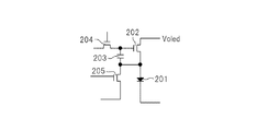
図29は、従来の有機EL(Electro Luminescence)ディスプレイの各画素回路を示す。図29に示すように、各画素回路は、有機EL素子201、駆動TFT(Thin Film-Transistor)202、容量203、TFTスイッチ204、及び、TFTスイッチ205を有する。
FIG. 29 shows each pixel circuit of a conventional organic EL (Electro Luminescence) display. As shown in FIG. 29, each pixel circuit includes an
具体的には、図29に示すように、有機EL素子201のアノードは、駆動TFT(Thin Film-Transistor)202を介して、電源Voledに接続され、カソードは、接地される。また、駆動TFT202のゲートには、TFTスイッチ204を介して、表示電圧に応じた信号が入力され、ソースには、TFTスイッチ205を介して、所定の電圧が入力される。容量203は、駆動TFT202のゲートソース間に接続される。
Specifically, as shown in FIG. 29, the anode of the
次に、当該各画素回路の動作について説明する。TFTスイッチ204及び205がオンすることにより、容量203の両端に、信号電圧と上記所定の電圧との電位差が保持される。その後、TFTスイッチ204及び205をオフすることにより、容量203の両端に保持された上記電位差が、駆動TFT202のゲートソース間に出力される。そして、駆動TFT202は、上記信号電圧に応じた駆動電流で有機EL素子201を発光させる。上記のような従来の画素回路は、例えば、特許第4052865号公報または特許第3877049号公報に開示されている。
Next, the operation of each pixel circuit will be described. When the
上記従来の画素回路は、各画素に設けられた有機EL素子201を、信号電圧に対応した輝度で発光させることができる。しかしながら、駆動TFT202は、薄膜トランジスタであるため、その電圧電流特性がゲート電圧印加によって経時変化するという問題がある。薄膜トランジスタは、単結晶で構成されていないために、チャネル界面においてキャリアトラップとなる準位が生成されやすく、また、分子間の結合に確率的に弱い部分を有している。したがって、このような準位におけるキャリアの出入りや、分子間結合の切断に起因する特性変化が電界ストレスによって容易に生じるからである。
The conventional pixel circuit can cause the
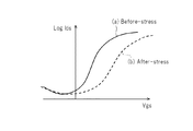
図30は、nチャネルのアモルファスSi−TFTのゲートソース間に、電圧ストレスを印加する前後のTFT特性を示した図である。具体的には、図30は、当該TFTのソースドレイン間に同一の電圧を印加した状態で、ゲートソース間に電圧ストレスを印加し、TFTの電圧電流特性の変化を実測した結果を示す。横軸は、ゲートソース間電圧を示し、縦軸は、ソースドレイン間電流を対数で示す。また、実線は、電圧ストレス印加前の電流特性、破線は、電圧ストレス印加後の電流特性を示す。 FIG. 30 is a diagram showing TFT characteristics before and after applying voltage stress between the gate and source of an n-channel amorphous Si-TFT. Specifically, FIG. 30 shows a result of actually measuring a change in the voltage-current characteristics of the TFT by applying a voltage stress between the gate and the source in the state where the same voltage is applied between the source and drain of the TFT. The horizontal axis shows the gate-source voltage, and the vertical axis shows the source-drain current in logarithm. A solid line indicates current characteristics before voltage stress application, and a broken line indicates current characteristics after voltage stress application.
図30に示すように、ゲートソース間に電圧ストレスを印加すると、当該TFTの閾値電圧(Vth)が(a)から(b)、つまり、高電圧側へシフトする。キャリア移動度(μ)で代表されるターンオン領域の電流値が低下し、また、サブスレッショルド領域におけるS値が低下する。 As shown in FIG. 30, when a voltage stress is applied between the gate and the source, the threshold voltage (Vth) of the TFT shifts from (a) to (b), that is, to the high voltage side. The current value in the turn-on region represented by carrier mobility (μ) decreases, and the S value in the subthreshold region decreases.
したがって、駆動TFT202におけるストレス起因の電圧電流特性の経時変化は、表示画面における一種の焼付きとなり、結果として、表示画面の画質が劣化する。これは、発光履歴の多い画素の駆動TFT202はゲート電圧ストレス履歴が多く、発光履歴の少ない画素の駆動TFT202は、ゲート電圧ストレス履歴が少ないからである。
Therefore, the time-dependent change in voltage-current characteristics due to stress in the driving
現時点では、有機EL素子を用いた表示装置は、当該有機EL素子自体の劣化が大きく、また、量産製品に用いられている低温多結晶Si−TFTは、上記ストレス経時変化が比較的小さいことから、上記の課題は、比較的顕在化していない。しかしながら、有機EL素子自体がより長寿命となった場合には、深刻な問題となる。現在の量産製品は、低温多結晶Si−TFTの閾値電圧のばらつきを補正するため、その回路が工夫されているが、上記ストレスにより経時変化するものは、上記閾値電圧Vthに限らずキャリア移動度(μ)やS値にも及ぶからである。 At present, a display device using an organic EL element has a large deterioration of the organic EL element itself, and a low-temperature polycrystalline Si-TFT used for a mass-produced product has a relatively small stress change with time. The above-mentioned problems are not relatively obvious. However, when the organic EL element itself has a longer lifetime, it becomes a serious problem. The current mass-produced products have been devised in order to correct variations in threshold voltage of low-temperature polycrystalline Si-TFTs, but those that change over time due to the stress are not limited to the threshold voltage Vth but carrier mobility. This is because it extends to (μ) and S values.
また、上記のようなストレス経時変化は、低温多結晶Si−TFTでは比較的小さいが、微結晶Si−TFTでは無視できず、例えば、アモルファスSi−TFT、有機TFT等では、極めて大きくなる。更に、製造コストの大幅な削減のため、現在量産製品に用いられている低温多結晶Si−TFTから、微結晶Si−TFT、アモルファスSi−TFT、有機TFT等への置換えが期待されているが、この際にはストレス経時変化に起因する上記の焼付きが深刻な課題となる。 In addition, the stress change with time as described above is relatively small in the low-temperature polycrystalline Si-TFT but cannot be ignored in the microcrystalline Si-TFT, and is extremely large in, for example, an amorphous Si-TFT, an organic TFT, and the like. Furthermore, in order to significantly reduce manufacturing costs, replacement of low-temperature polycrystalline Si-TFTs currently used in mass-produced products with microcrystalline Si-TFTs, amorphous Si-TFTs, organic TFTs, etc. is expected. In this case, the above-mentioned seizure resulting from the stress change with time becomes a serious problem.
(1)上記の課題を解決するため、本発明に係る表示装置は、発光素子と、前記発光素子への駆動電流を制御する駆動トランジスタと、階調値に対応する電圧が書き込まれ保持するとともに、前記駆動トランジスタのゲートソース間に前記階調値に対応する電圧に応じた表示電圧を印加するための保持容量と、をそれぞれ有する複数の画素と、前記駆動トランジスタのゲートソース間に、前記表示電圧の取り得る値の範囲外の電圧値を有するストレス電圧を印加するストレス電圧印加手段と、を有する。 (1) In order to solve the above-described problem, a display device according to the present invention has a light emitting element, a driving transistor for controlling a driving current to the light emitting element, and a voltage corresponding to a gradation value written and held. A plurality of pixels each having a storage capacitor for applying a display voltage corresponding to the voltage corresponding to the gradation value between the gate and source of the driving transistor, and the display between the gate and source of the driving transistor. Stress voltage applying means for applying a stress voltage having a voltage value outside the range of values that the voltage can take.
(2)上記(1)に記載の表示装置において、前記ストレス電圧印加手段は、前記表示電圧の取り得る値の範囲の上限値よりも高い電圧値を有する高電圧値、または、前記表示電圧の取り得る値の範囲の下限値よりも低い電圧値を有する低電圧値の一方を印加し、前記表示装置は、更に、前記駆動トランジスタのゲートソース間に、前記高電圧値を印加する場合には、前記高電圧値よりも低い電圧値を印加し、前記低電圧値を印加する場合には、前記低電圧値よりも高い電圧値を有する緩和電圧を印加する緩和電圧印加手段を有してもよい。 (2) In the display device according to (1), the stress voltage applying unit may be a high voltage value having a voltage value higher than an upper limit value of a range of the display voltage, or the display voltage. When one of the low voltage values having a voltage value lower than the lower limit value of the range of possible values is applied, and the display device further applies the high voltage value between the gate and source of the driving transistor, In the case of applying a voltage value lower than the high voltage value and applying the low voltage value, there is provided relaxation voltage application means for applying a relaxation voltage having a voltage value higher than the low voltage value. Good.
(3)上記(2)に記載の表示装置において、前記緩和電圧は、前記表示電圧の取り得る値の範囲内の電圧値であってもよい。 (3) In the display device according to (2), the relaxation voltage may be a voltage value within a range of values that the display voltage can take.
(4)上記(3)に記載の表示装置において、前記緩和電圧は、前記ストレス電圧印加手段が前記表示電圧の取り得る値の範囲の上限値よりも高い電圧値を印加する場合には、前記下限値を有し、前記ストレス電圧印加手段が、前記表示電圧の取り得る値の範囲の上限値よりも高い電圧値を印加する場合には、前記上限値を有してもよい。 (4) In the display device according to (3), when the stress voltage application unit applies a voltage value higher than an upper limit of a range of values that can be taken by the display voltage, When the stress voltage application unit has a lower limit value and applies a voltage value higher than the upper limit value of the range of values that the display voltage can take, the upper limit value may be included.
(5)上記(2)に記載の表示装置において、前記緩和電圧印加手段は、前記ストレス電圧印加手段が前記ストレス電圧を印加した後に、前記緩和電圧を印加してもよい。 (5) In the display device according to (2), the relaxation voltage application unit may apply the relaxation voltage after the stress voltage application unit has applied the stress voltage.
(6)上記(2)に記載の表示装置において、前記複数の画素は、マトリクス状に配置され、前記表示装置は、更に、前記表示電圧を生成する表示電圧発生手段と、前記表示電圧を前記各画素に入力する信号線と、前記各発光素子に発光電力を供給する電源線と、を有し、前記各画素は、更に、画素スイッチを有し、前記駆動トランジスタは電界効果トランジスタであって、前記保持容量は、前記駆動トランジスタのゲートソース間に配置され、前記電界効果トランジスタのソースまたはドレインの一方は、前記電源線に、他方は前記発光素子に接続され、前記電界効果トランジスタのゲートは、前記画素スイッチを介して、前記信号線に接続されてもよい。 (6) In the display device according to (2), the plurality of pixels are arranged in a matrix, and the display device further includes a display voltage generating unit that generates the display voltage, and the display voltage. A signal line that inputs to each pixel; and a power supply line that supplies light emission power to each light emitting element. Each pixel further includes a pixel switch, and the drive transistor is a field effect transistor. The storage capacitor is disposed between the gate and source of the driving transistor, one of the source and drain of the field effect transistor is connected to the power supply line, the other is connected to the light emitting element, and the gate of the field effect transistor is The signal line may be connected via the pixel switch.
(7)上記(6)に記載の表示装置において、前記表示電圧、前記ストレス電圧に対応するストレス入力電圧、及び、前記緩和電圧に対応する緩和入力電圧を、前記信号線を介して、前記各画素に入力してもよい。 (7) In the display device according to (6), the display voltage, the stress input voltage corresponding to the stress voltage, and the relaxation input voltage corresponding to the relaxation voltage are transmitted through the signal lines. You may input into a pixel.
(8)上記(7)に記載の表示装置において、前記表示電圧発生手段は、更に、選択スイッチを有し、前記表示電圧発生手段は、前記表示電圧、前記ストレス入力電圧、または、前記緩和入力電圧を、前記選択スイッチを介して、選択的に出力してもよい。 (8) In the display device according to (7), the display voltage generation unit further includes a selection switch, and the display voltage generation unit includes the display voltage, the stress input voltage, or the relaxation input. The voltage may be selectively output via the selection switch.
(9)上記(7)に記載の表示装置において、前記表示電圧発生手段は、更に、選択スイッチを有し、前記表示電圧発生手段は、前記ストレス入力電圧、または、前記緩和入力電圧を、前記選択スイッチを介して、選択的に出力してもよい。 (9) In the display device according to (7), the display voltage generation unit further includes a selection switch, and the display voltage generation unit receives the stress input voltage or the relaxation input voltage. You may selectively output via a selection switch.
(10)上記(7)に記載の表示装置において、前記ストレス入力電圧は、前記電源線を介して、前記各画素へ入力してもよい。 (10) In the display device according to (7), the stress input voltage may be input to each pixel through the power supply line.
(11)上記(6)に記載の表示装置は、更に、前記信号線に対して垂直方向に設けられたストレス電圧線を有し、前記ストレス入力電圧及び前記緩和入力電圧を、前記ストレス電圧線を介して、前記複数の画素へ入力してもよい。 (11) The display device according to (6) further includes a stress voltage line provided in a direction perpendicular to the signal line, and the stress input voltage and the relaxed input voltage are transmitted to the stress voltage line. It is also possible to input to the plurality of pixels via.
(12)上記(6)に記載の表示装置において、前記各画素は、更に、発光制御スイッチを有し、前記電界効果トランジスタは、nMOSであり、前記電界効果トランジスタのソース端子は、前記発光素子に接続され、ドレイン端子は、前記発光制御スイッチを介して、前記電源線に接続され、前記ストレス電圧を前記保持容量に印加する際、前記発光制御スイッチは、オフ状態に固定されてもよい。 (12) In the display device according to (6), each of the pixels further includes a light emission control switch, the field effect transistor is an nMOS, and the source terminal of the field effect transistor is the light emitting element. The drain terminal is connected to the power supply line via the light emission control switch, and the light emission control switch may be fixed to an off state when the stress voltage is applied to the storage capacitor.
(13)上記(6)に記載の表示装置において、前記各画素は、更に、発光制御スイッチを有し、前記電界効果トランジスタは、nMOSであり、前記電界効果トランジスタのソース端子は、前記発光素子に接続され、ドレイン端子は、前記発光制御スイッチを介して、前記電源線に接続され、前記緩和電圧を前記保持容量に印加する際、前記発光制御スイッチは、オフ状態に固定されてもよい。 (13) In the display device according to (6), each pixel further includes a light emission control switch, the field effect transistor is an nMOS, and a source terminal of the field effect transistor is the light emitting element. The drain terminal is connected to the power supply line via the light emission control switch, and the light emission control switch may be fixed to an off state when the relaxation voltage is applied to the storage capacitor.
(14)上記(6)に記載の表示装置において、前記各画素は、更に、発光制御スイッチを有し、前記電界効果トランジスタは、nMOSであり、前記電界効果トランジスタのソース端子は、前記発光素子に接続され、ドレイン端子は、前記発光制御スイッチを介して、前記電源線に接続され、前記表示電圧を前記保持容量に印加する際、前記発光制御スイッチは、オフ状態に固定されてもよい。 (14) In the display device according to (6), each of the pixels further includes a light emission control switch, the field effect transistor is an nMOS, and the source terminal of the field effect transistor is the light emitting element. The drain terminal is connected to the power supply line via the light emission control switch, and when the display voltage is applied to the storage capacitor, the light emission control switch may be fixed in an off state.
(15)上記(1)に記載の表示装置において、前記各画素は、更に、発光制御スイッチを有し、前記電界効果トランジスタは、pMOSであり、前記電界効果トランジスタのソース端子は、前記電源線に接続され、ドレイン端子は、前記発光制御スイッチを介して、前記発光素子に接続され、前記ストレス電圧を前記保持容量に印加する際、前記発光制御スイッチは、オフ状態に固定されてもよい。 (15) In the display device according to (1), each of the pixels further includes a light emission control switch, the field effect transistor is a pMOS, and a source terminal of the field effect transistor is the power line. The drain terminal is connected to the light emitting element via the light emission control switch, and the light emission control switch may be fixed to an off state when applying the stress voltage to the storage capacitor.
(16)上記(1)に記載の表示装置において、前記各画素は、更に、発光制御スイッチを有し、前記電界効果トランジスタは、pMOSであり、前記電界効果トランジスタのソース端子は、前記電源線に接続され、ドレイン端子は、前記発光制御スイッチを介して、前記発光素子に接続され、前記緩和電圧を前記保持容量に印加する際、前記発光制御スイッチは、オフ状態に固定されてもよい。 (16) In the display device according to (1), each of the pixels further includes a light emission control switch, the field effect transistor is a pMOS, and a source terminal of the field effect transistor is the power line. The drain terminal is connected to the light emitting element via the light emission control switch, and the light emission control switch may be fixed in an off state when the relaxation voltage is applied to the storage capacitor.
(17)上記(1)に記載の表示装置において、前記各画素は、更に、発光制御スイッチを有し、前記電界効果トランジスタは、pMOSであり、前記電界効果トランジスタのソース端子は、前記電源線に接続され、ドレイン端子は、前記発光制御スイッチを介して、前記発光素子に接続され、前記表示電圧を前記保持容量に印加する際、前記発光制御スイッチは、オフ状態に固定されてもよい。 (17) In the display device according to (1), each of the pixels further includes a light emission control switch, the field effect transistor is a pMOS, and a source terminal of the field effect transistor is the power line. The drain terminal is connected to the light emitting element via the light emission control switch, and when the display voltage is applied to the storage capacitor, the light emission control switch may be fixed in an off state.
(18)上記(6)に記載の表示装置において、前記各画素は、更に、チャネルスイッチと、所定の定電圧が印加される低電圧配線とを有し、前記電界効果トランジスタのドレイン端子は、前記第1のチャネルスイッチを介して、前記低電圧配線に接続されてもよい。 (18) In the display device according to (6), each pixel further includes a channel switch and a low-voltage wiring to which a predetermined constant voltage is applied, and the drain terminal of the field effect transistor is The first voltage switch may be connected to the low voltage wiring.
(19)上記(18)に記載の表示装置において、前記チャネルスイッチのゲートは、前記画素スイッチのゲートと共通に接続され、前記複数の画素は、前記チャネルスイッチを介して、行毎に制御されてもよい。 (19) In the display device according to (18), a gate of the channel switch is commonly connected to a gate of the pixel switch, and the plurality of pixels are controlled for each row through the channel switch. May be.
(20)上記(6)に記載の表示装置において、前記各画素は、更に、第1のチャネルスイッチと、第2のチャネルスイッチと、所定の定電圧が印加された低電圧配線とを有し、前記電界効果トランジスタのドレイン端子は、前記第1のチャネルスイッチを介して、前記低電圧配線に接続され、ソース端子は、前記第2のチャネルスイッチを介して、前記低電圧配線に接続されてもよい。 (20) In the display device according to (6), each of the pixels further includes a first channel switch, a second channel switch, and a low voltage wiring to which a predetermined constant voltage is applied. The drain terminal of the field effect transistor is connected to the low voltage wiring through the first channel switch, and the source terminal is connected to the low voltage wiring through the second channel switch. Also good.
(21)上記(20)に記載の表示装置において、前記第1及び第2のチャネルスイッチのゲートは、前記画素スイッチのゲートと共通に接続され、前記複数の画素は、前記第1及び第2のチャネルスイッチを介して、行毎に制御されてもよい。 (21) In the display device according to (20), gates of the first and second channel switches are commonly connected to gates of the pixel switches, and the plurality of pixels include the first and second pixels. It may be controlled for each row through the channel switch.
(22)上記(18)に記載の表示装置において、前記低電圧配線は、前記複数の画素のうち、隣接する画素間で共通に接続されてもよい。 (22) In the display device according to (18), the low-voltage wiring may be commonly connected between adjacent pixels among the plurality of pixels.
(23)上記(18)に記載の表示装置において、前記発光素子の前記電界効果トランジスタに接続されていない端子は、前記複数の画素のうち、隣接する画素間で共通に接地され、前記低電圧配線は、前記各画素内で接地されてもよい。 (23) In the display device according to (18), a terminal of the light emitting element that is not connected to the field effect transistor is commonly grounded between adjacent pixels among the plurality of pixels, and the low voltage The wiring may be grounded in each pixel.
(24)上記(6)に記載の表示装置において、前記電界効果トランジスタのソース端子は、前記発光素子の一端に接続され、前記電界効果トランジスタのドレイン端子は、前記電源線に接続され、前記表示電圧が前記保持容量に印加される際、前記電源線の電圧を、前記発光素子の他端に印加される電圧と等しい電圧としてもよい。 (24) In the display device according to (6), a source terminal of the field effect transistor is connected to one end of the light emitting element, a drain terminal of the field effect transistor is connected to the power supply line, and the display When a voltage is applied to the storage capacitor, the voltage of the power supply line may be equal to the voltage applied to the other end of the light emitting element.
(25)上記(6)に記載の表示装置において、前記電界効果トランジスタのソース端子は、前記発光素子の一端に接続され、前記電界効果トランジスタのドレイン端子は、前記電源線に接続され、前記ストレス電圧が前記保持容量に印加される際、前記電源線の電圧を、前記発光素子の他端に印加される電圧と等しい電圧としてもよい。 (25) In the display device according to (6), a source terminal of the field effect transistor is connected to one end of the light emitting element, a drain terminal of the field effect transistor is connected to the power supply line, and the stress When a voltage is applied to the storage capacitor, the voltage of the power supply line may be equal to the voltage applied to the other end of the light emitting element.
(26)上記(6)に記載の表示装置において、前記電界効果トランジスタのソース端子は、前記発光素子の一端に接続され、前記電界効果トランジスタのドレイン端子は、前記電源線に接続され、前記緩和電圧が前記保持容量に印加される際、前記電源線の電圧を、前記発光素子の他端に印加される電圧と等しい電圧としてもよい。 (26) In the display device according to (6), a source terminal of the field effect transistor is connected to one end of the light emitting element, a drain terminal of the field effect transistor is connected to the power supply line, and the relaxation is performed. When a voltage is applied to the storage capacitor, the voltage of the power supply line may be equal to the voltage applied to the other end of the light emitting element.
(27)上記(6)に記載の表示装置は、1フレームの期間内に、前記表示電圧を前記複数の画素に線順次で前記保持容量に書込んだ後、前記ストレス電圧及び前記緩和電圧を前記複数の画素に一括で前記保持容量に書込んでもよい。 (27) In the display device according to (6), the display voltage is written to the storage capacitor in a line sequential manner in the plurality of pixels within one frame period, and then the stress voltage and the relaxation voltage are applied. The plurality of pixels may be written into the storage capacitor at once.
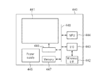
(28)上記(1)に記載の表示装置は、更に、前記表示電圧に対応する表示データを蓄積するメモリと、前記表示データから前記表示電圧を発生する表示電圧発生手段と、前記表示装置を駆動する電力を供給する供給装置と、を有してもよい。 (28) The display device according to (1) further includes a memory for storing display data corresponding to the display voltage, display voltage generating means for generating the display voltage from the display data, and the display device. And a supply device that supplies electric power to be driven.
ストレス電圧の印加により、駆動TFTの特性変化に起因する焼付きを解消することができる。 By applying the stress voltage, it is possible to eliminate burn-in caused by the change in characteristics of the driving TFT.
以下、本発明の実施の形態について、図面を参照しつつ説明する。なお、図面については、同一又は同等の要素には同一の符号を付し、重複する説明は省略する。 Embodiments of the present invention will be described below with reference to the drawings. In addition, about drawing, the same code | symbol is attached | subjected to the same or equivalent element, and the overlapping description is abbreviate | omitted.
[第1の実施形態]
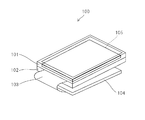
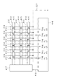
図1は、本発明の第1の実施形態に係る表示装置を示す図である。図1に示すように、有機EL表示装置100は、有機ELパネルを有するTFT(Thin Film Transistor)基板105を挟むように固定する上フレーム101及び下フレーム102と、表示する情報を生成する回路素子を備える回路基板104と、当該回路基板において生成されたRGBの情報をTFT基板105に伝えるフレキシブル基板103と、により構成される。
[First embodiment]
FIG. 1 is a diagram showing a display device according to a first embodiment of the present invention. As shown in FIG. 1, an organic
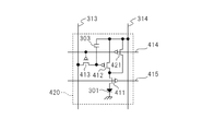
図2は、本発明の第1の実施形態における表示装置の各画素を概略的に示す図である。図2に示すように、各画素310には、有機EL素子301が設けられ、有機EL素子301の一端は、共通カソード電極に接地され、他端は、駆動TFT302と発光制御スイッチ306を介して、電源線314に接続される。
FIG. 2 is a diagram schematically showing each pixel of the display device according to the first embodiment of the present invention. As shown in FIG. 2, each
駆動TFT302のゲートは、ゲートスイッチ304を介して信号線313に接続される。駆動TFT302のドレインは、チャネルスイッチ307を介して低電圧線315に接続される。また、駆動TFT302のゲートソース間には、保持容量303が設けられる。
The gate of the driving
発光制御スイッチ306のゲートは、発光制御線311に接続される。発光制御スイッチ306のソースは、電源線314に接続され、ドレインは、駆動TFT302のドレイン及びチャネルスイッチ307のドレインに接続される。
The gate of the light
チャネルスイッチ307及びゲートスイッチ304のゲートは、ゲート走査線312に接続される。なお、各スイッチ307等及び駆動TFT302は、例えば、そのサイズ以外は同一の基本構造を有するnチャネルのアモルファスSi−TFTで構成され、ガラス基板上に設けてもよい。
The gates of the
図3は、図2に示した各画素の配置図を示す。図3に示すように、隣接する左右の画素310は、電源線314及び低電圧線315を共有する。したがって、画素310の配置を簡略化し、製造過程における歩留を減少することができる。なお、図3は、説明の簡略化のため、横4ドット、縦2ドットの計8個分の画素310のみを示すが、必要に応じてその他の数の画素が配置され得ることはいうまでもない。
FIG. 3 is a layout diagram of each pixel shown in FIG. As shown in FIG. 3, adjacent left and
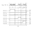
次に、本実施の形態にかかる画素310の動作の概略について説明する。図4は、画素の動作を説明するための図である。図4の横方向は、各画素310の縦方向の配列(列、row)を示し、横方向に第1列目から最終列までの画素310に対応する。一方、図4の縦方向は、各画素310の時間軸(time)を表しており、縦方向の長さが1フレーム期間(例えば、1/60秒)に相当する。
Next, an outline of the operation of the
また、斜めに記載された実線は、各画素列の走査タイミングを示す。具体的には、実線435は、保持容量303への表示電圧の書込みを示す。また、実線436は、駆動TFT302へのストレス電圧の印加を開始するタイミングを示し、実線437は、駆動TFT302への緩和電圧の印加を開始するタイミングを示す。
Moreover, the solid line described diagonally indicates the scanning timing of each pixel column. Specifically, a
図4の期間Aは、駆動TFT302による有機EL素子301の発光期間を示し、期間Bは、駆動TFT302に対するストレス電圧印加期間を示す。また、期間Cは、駆動TFT302に対する緩和電圧印加期間を示す。
A period A in FIG. 4 indicates a light emission period of the
例えば、第1列目の画素310について説明すると、まず、実線435に示す保持容量303への表示電圧の書込みが行われ、その後の発光期間Aにおいて、有機EL素子301が発光される。次の実線436に始まる期間Bにおいては、駆動TFT302へストレス電圧が印加される。次の実線437に始まる期間Cにおいては、駆動TFT302へ緩和電圧が印加される。上記のような動作が1フレーム期間毎に繰り返し行われる。
For example, the
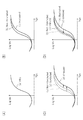
次に、上記のような動作における駆動TFT302に対する電圧ストレスに関して説明する。図5(A)乃至(D)及び図6(A)乃至(D)は、ゲート電圧ストレスに起因する駆動TFTの特性変化の概念について説明するための図である。
Next, voltage stress on the driving
具体的には、図5(A)乃至(D)及び図6(A)乃至(D)は、駆動TFTのソースドレイン間に同一の電圧を印加した状態における駆動TFTの特性を示す。また、横軸は、駆動TFT302のゲートソース間電圧を示し、縦軸は、駆動TFT302のソースドレイン間電流を対数で示す。なお、図5(A)乃至(D)と図6(A)乃至(D)は、ストレス電圧及び緩和電圧の印加の方向が逆である点が異なり、その他の点は同様である。
Specifically, FIGS. 5A to 5D and FIGS. 6A to 6D show characteristics of the driving TFT in a state where the same voltage is applied between the source and drain of the driving TFT. The horizontal axis indicates the gate-source voltage of the driving
図5(A)及び図6(A)は、駆動TFTの初期状態を示す図である。図5(B)及び図6(B)は、図4における発光期間A後の駆動TFTの特性を示す図である。図5(B)及び図6(B)に示すように、有機EL素子301を駆動した駆動TFT302の特性(c)は、有機EL素子301を駆動していない駆動TFT302の特性と異なる特性(b)を有する。
FIG. 5A and FIG. 6A are diagrams showing an initial state of the driving TFT. FIGS. 5B and 6B are diagrams showing the characteristics of the driving TFT after the light emission period A in FIG. As shown in FIGS. 5B and 6B, the characteristic (c) of the driving
これは、有機EL素子301を駆動していない駆動TFT302(Non-illuminated)の特性(b)は、有機EL素子301を駆動していないことから、図5(A)及び図6(A)に示した(a)initialと同じであるのに対し、有機EL素子301を駆動した駆動TFT302(illuminated)の特性(c)は、前述したゲート電圧印加に起因する経時変化により、その特性に変化が生じるからである。
This is because the characteristic (b) of the driving TFT 302 (Non-illuminated) that does not drive the
図5(C)及び図6(C)は、図4に示した期間Bに、駆動TFTのゲートソース間にストレス電圧を印加した後の駆動TFT302の特性を示す図である。ここで、ストレス電圧は、表示電圧の取り得る範囲外の電圧値を有し、好ましくは表示電圧の取り得る範囲の電圧値よりも十分に高い電圧値、または、低い電圧値を有する。
5C and 6C are diagrams illustrating characteristics of the driving
具体的には、例えば、当該ストレス電圧は、図5(C)に示すように、上記(c)で示した特性を与える電圧よりも十分に高い電圧値、または、図6(C)に示すように、上記(b)で示した特性を与える電圧よりも十分に低い電圧値を有する。いいかえれば、表示電圧の取り得る範囲の電圧値よりも過剰な電圧値を有する。 Specifically, for example, as shown in FIG. 5C, the stress voltage is sufficiently higher than the voltage giving the characteristics shown in (c) above, or shown in FIG. 6C. Thus, it has a voltage value sufficiently lower than the voltage giving the characteristics shown in (b) above. In other words, it has an excessive voltage value than the voltage value in the range that the display voltage can take.
図5(D)及び図6(D)は、図4に示した期間Cに駆動TFTのゲートソース間に緩和電圧を印加した後の駆動TFTの特性を示す図である。図5(D)及び図6(D)に示すように(illuminated)と(Non-illuminated)の特性(c)及び(b)は、両者ともに同等な特性(d)(stressed)に変化する。ゲート電圧印加に起因する経時変化は、ゲート電圧に対する依存性が極めて大きいため、ストレス電圧に起因するゲート電圧ストレスと比較すると期間Aにおける発光素子駆動におけるストレスの有無は無視し得るからである。 5D and 6D are diagrams illustrating the characteristics of the drive TFT after a relaxation voltage is applied between the gate and source of the drive TFT in the period C illustrated in FIG. As shown in FIG. 5D and FIG. 6D, the characteristics (c) and (b) of (illuminated) and (Non-illuminated) both change to equivalent characteristics (d) (stressed). This is because the temporal change due to the application of the gate voltage is very dependent on the gate voltage, so that the presence or absence of stress in the light emitting element driving in the period A can be ignored as compared with the gate voltage stress caused by the stress voltage.
上記のようにして、ストレス電圧の印加により、駆動TFT302の特性変化に起因する焼付きを解消することができる。
As described above, the image sticking caused by the characteristic change of the driving
しかしながら、上記のようなストレス電圧の印加は、図5(C)または図6(C)に示すように、当該ストレス電圧を印加しない場合と比べ、全ての駆動TFT302の特性をより大きく変動させる。よって、駆動TFT302の閾値電圧Vthがより大きくなり、同一の表示電圧に対して駆動される電流量が著しく減少する場合がある。したがって、このままの駆動を続けていると急激にディスプレイの輝度が低下してしまい、最終的に表示装置は発光することができなくなり得る。
However, the application of the stress voltage as described above causes the characteristics of all the
そこで、更に、図4に示した期間Cにおいて、駆動TFT302に対して、緩和電圧を印加する。ここで、緩和電圧は、図5(D)に示すように、上記ストレス電圧値よりも低い電圧値(図5D右方向)、または、図6(D)に示すように、上記ストレス電圧値よりも高い電圧値(図5D左方向)を有する。好ましくは、上記緩和電圧は、表示電圧の取り得る値の範囲内の電圧値を有するようにすればよい。また、より好ましくは、表示電圧の取り得る値の範囲内の電圧値のうち、最小の電圧値を有するようにすればよい。つまり、緩和電圧の極性は、ストレス電圧の極性と逆極性である場合も含まれる。
Therefore, a relaxation voltage is further applied to the driving
これにより、図5(D)及び図6(D)に示すように、(d)(stressed)の特性は(e)(relieved)にまで緩和される。このとき、(e)(relieved)の特性は、図5(D)及び図6(D)に示した(b)(Non-illuminated)と(c)(illuminated)の特性の間に来る程度の特性となる。 Thereby, as shown in FIGS. 5D and 6D, the characteristic of (d) (stressed) is relaxed to (e) (relieved). At this time, the characteristics of (e) (relieved) are between the characteristics of (b) (Non-illuminated) and (c) (illuminated) shown in FIGS. 5 (D) and 6 (D). It becomes a characteristic.
このように、緩和電圧の印加期間を設けることにより、ストレス電圧による駆動TFT302の過剰な特性変化を回復させることができる。結果として、長期間に渡る安定した輝度での表示が可能となる。いいかえれば、ストレス電圧印加による駆動TFT302のより大きい特性変動を、均一に回復することができ、駆動回路に起因する焼付きや輝度低下を生じない表示装置100を実現することができる。
As described above, by providing the relaxation voltage application period, it is possible to recover an excessive characteristic change of the driving
次に、上記のようにストレス電圧及び緩和電圧を印加するための駆動回路について説明する。図7は、第1の実施形態における駆動回路の概略を示す図である。なお、図7は、説明の簡略化のために、6×3ドットの画素310のみを示しているが、必要に応じてその他の画素数が用いられることはいうまでもない。また、所望の解像度に応じて、表示単位である横方向3ドットの画素310には、それぞれ赤(R)、緑(G)、青(B)の3色の有機EL素子301が設けられ得ることはいうまでもない。
Next, a driving circuit for applying the stress voltage and the relaxation voltage as described above will be described. FIG. 7 is a diagram showing an outline of the drive circuit in the first embodiment. Note that FIG. 7 shows only the 6 × 3
図7に示すように、発光制御線311およびゲート走査線312の一端は、垂直走査回路331に接続される。また、上述のように、各画素310には、水平方向に配置された発光制御線311およびゲート走査線312が接続される。
As shown in FIG. 7, one end of the light
電源線314と低電圧線315は、それぞれ電源入力線327と低電圧線入力線328に接続される。また、電源入力線327と低電圧線入力線328には、例えば、それぞれ10Vと0Vが外部の電圧供給源(図示せず)より入力される。
The
信号線313は、対応するRGBの発光色別に、切替えスイッチ321、322、323を介して、ドライバIC330に接続される。また、切替えスイッチ321、322、323のゲート走査線324、325、326及び垂直走査回路331の制御線群332はドライバIC330に接続される。
The
ドライバIC330は、複数のスイッチ701を有し、各スイッチ701は、入力側に信号電圧VSig、高電圧VH、低電圧VLの入力端子がそれぞれ接続され、出力側は、切替えスイッチ321、322、323に接続される。そして、ドライバIC330は、当該各スイッチ701により、ドライバIC330に入力される信号電圧VSig、高電圧VH、低電圧VLのいずれかを、切替えスイッチ321、322、323に出力する。なお、例えば、信号電圧VSigは、0〜5V、高電圧VHは、7V、低電圧VLは、0Vの電圧値を有する。
The
ここで、各スイッチ321等及び垂直走査回路331は、サイズ以外は同一の基本構造を有するnチャネルのアモルファスSi−TFTで構成されてもよく、また、画素310と同一のガラス基板上に設けてもよい。また、ドライバIC330は、例えば、Si半導体チップであり、当該ガラス基板上にCOG(Chip-On Glass)実装されてもよい。
Here, the
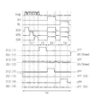
次に、上記駆動回路の具体的な動作を説明する。図8は、本実施の形態における駆動回路の動作タイミング図である。横方向は時間軸であり、1水平走査期間(1H)を示す。Vsigは、ドライバIC330における信号出力電圧、VHは、ドライバIC330における高電圧出力、VLは、ドライバIC330における低電圧出力、324、325、326はゲート走査線324、325、326の出力に対応し、それぞれ上がオン、下がオフである。なお、Vsig、VH、VL、324、325、326は1H毎に繰返す信号である。
Next, a specific operation of the drive circuit will be described. FIG. 8 is an operation timing chart of the drive circuit in the present embodiment. The horizontal direction is a time axis and indicates one horizontal scanning period (1H). Vsig corresponds to the signal output voltage in the
また、図8の下半分のタイミング図は、タイミングt1、t2、t3、t4における発光制御線311及びゲート走査線312の走査タイミングをそれぞれ示す。なお、タイミングt1、t2、t3、t4は、図4に示したt1、t2、t3、t4に対応し、それぞれ時刻t1、t2、t3、t4における第1列目の画素の動作と対応している。
The timing chart in the lower half of FIG. 8 shows scanning timings of the light
以下、1H期間を図8に示すように、T1、T2、T3、T4の期間に分けて順次説明する。図8に示すように、1フレーム期間においては、1H期間におけるT2期間のはじまりでゲート走査線312がオンされ、T2期間の終わりでオフされる。一方、発光制御線311は、当該1H期間のT4期間の終わりでオンされる。タイミングt3までの期間は当該状態(例えば、図8のt2で示す状態)が続く。
Hereinafter, as shown in FIG. 8, the 1H period will be described in order by dividing it into periods of T1, T2, T3, and T4. As shown in FIG. 8, in one frame period, the
その後、タイミングt3のT1期間のはじまりで、発光制御線311は、オフされる。一方、ゲート走査線312は、T3期間の始まりでオンされ、終わりでオフされる。その後、タイミングt4のT4期間の始まりまで、当該状態が続く。
Thereafter, at the beginning of the T1 period at the timing t3, the light
その後、タイミングt4のT4の始まりでゲート走査線312がオンされ、終わりでオフされる。上記のような動作が1フレーム期間毎に繰り返し行われる。以下、具体的に、各期間T1乃至T4の上記駆動回路及び画素回路の動作について説明する。
Thereafter, the
図8に示すように、1H期間における期間T1には、ドライバIC330からRGBの順に信号出力電圧が出力され、これがゲート走査線324、325、326によって走査される切替えスイッチ321、322、323により、信号線313上に出力される。発光制御線311及びゲート走査線312は、図4に示すタイミングt1、t3、及びt4において、共にオフされている。
As shown in FIG. 8, in the period T1 in the 1H period, signal output voltages are output from the
期間T2には、タイミングt1において、ゲート走査線312がオンすることによって、当該画素のゲートスイッチ304及びチャネルスイッチ307がオンされる。ここで、信号線313の出力電圧がある程度の発光信号を有するときは、駆動TFT302はオンし、低電圧線315の電圧である0Vがチャネルスイッチ307と駆動TFT302を介して、有機EL素子301のアノードに書込まれる。よって、保持容量303の両端には表示電圧として、信号線313の出力電圧がそのまま書込まれる。
In the period T2, the
一方、信号線313の出力電圧が殆んど発光信号を有さないときは、駆動TFT302はオンしないため、保持容量303の両端に、信号線313の出力電圧が、有機EL素子301の端子間容量との容量分割で書込まれる。ここで、有機EL素子301のアノード電圧の初期値は0Vであり、また、有機EL素子301の端子間容量は十分に大きいため、書込まれる表示電圧は、信号線313の出力電圧の90%程度の値となる。
On the other hand, when the output voltage of the
期間T3には、ドライバIC330から電圧VH(7V)が出力され、当該電圧VHが、ゲート走査線324、325、326によって同時にオンされる切替えスイッチ321、322、323を介して、信号線313に出力される。
In the period T3, a voltage VH (7V) is output from the
ここで、タイミングt3においては、ゲート走査線312がオンすることによって、当該画素のゲートスイッチ304及びチャネルスイッチ307がオンされる。このとき、ゲートスイッチ304から信号線313を介して、駆動TFT302のゲートにはVH(7V)が書込まれるため、駆動TFT302はオンし、低電圧線315の電圧である0Vが、チャネルスイッチ307と駆動TFT302を介して、有機EL素子301のアノードに書込まれる。よって、保持容量303の両端には表示電圧に替えてVH(7V)がそのまま書込まれる。
Here, at the timing t3, when the
期間T4にはドライバIC330から電圧VL(0V)が出力され、当該電圧VLがゲート走査線324、325、326によって同時にオンされる切替えスイッチ321、322、323によって、信号線313に出力される。ここで、タイミングt4においては、ゲート走査線312がオンすることにより、当該画素のゲートスイッチ304及びチャネルスイッチ307がオンされる。
In the period T4, the voltage VL (0 V) is output from the
このとき、ゲートスイッチ304から信号線313を介して駆動TFT302のゲートにはVL(0V)が書込まれるため、駆動TFT302はオフし、保持容量303の両端にはVL(0V)が、有機EL素子3011の端子間容量との容量分割で書込まれる。
At this time, since VL (0 V) is written from the
ここで、有機EL素子301のアノードにはタイミングt3で既に0Vが書込まれており、また有機EL素子301の端子間容量は十分に大きいため、VL(0V)がほぼそのまま保持容量303の両端に書込まれる。なお、前述のように、有機EL素子301のアノードの電圧は、タイミングt1に至るまで、このままほぼ0Vを維持すると考えて良い。
Here, 0 V has already been written to the anode of the
次に、1フレーム期間の観点から、駆動回路の具体的な動作につき説明する。タイミングt1からt3までの間の期間であって、タイミングt2に代表される期間A(有機EL素子301の発光期間)には、発光制御線311がオンすることによって、発光制御スイッチ306がオン状態に固定される。
Next, a specific operation of the drive circuit will be described from the viewpoint of one frame period. In a period from timing t1 to t3, which is a period A represented by timing t2 (light emission period of the organic EL element 301), the light
上記のように、既に、タイミングt1において保持容量303の両端には、表示電圧が書込まれており、この表示電圧が駆動TFT302のゲートソース間に印加されるため、駆動TFT302は表示電圧に対応した電流で、有機EL素子301を発光させる。なお、この期間Aは、例えば、1フレーム期間の約半分程度である。
As described above, the display voltage is already written to both ends of the
次に、発光制御線311がオフすることによって発光制御スイッチ306がオフした後、タイミングt3でストレス電圧VH(7V)が駆動TFT302のゲートソース間に設けられた保持容量303に書込まれ、期間Bの間保持される。
Next, after the light
次に、タイミングt4で緩和電圧VL(0V)が駆動TFT302のゲートソース間に設けられた保持容量303に書込まれた後期間Cの間保持される。その後、最初のタイミングt1に戻り新たな表示電圧が書込まれる。上記のような動作が1フレーム期間毎に繰り返される。
Next, the relaxation voltage VL (0 V) is written in the
上記のように、本実施の形態によれば、ストレス電圧の印加により、駆動TFT302の特性変化に起因する焼付きを解消することができる。また、緩和電圧の印加期間を設けることにより、ストレス電圧による駆動TFT302の過剰な特性変化を回復させることができる。結果として、長期間に渡る安定した輝度での表示が可能となる。いいかえれば、ストレス電圧印加による駆動TFT302のより大きい特性変動に対して均一に特性変動を回復することができ、駆動回路に起因する焼付きや輝度低下を生じない表示装置を実現することができる。
As described above, according to the present embodiment, it is possible to eliminate burn-in due to the characteristic change of the driving
また、本実施の形態は、特に、ドライバIC330がストレス電圧VH(7V)及び緩和電圧VL(0V)を含む信号線313駆動電圧を生成するために、例えばガラス基板上に設けるTFT回路を小規模化できるため、額縁領域の縮小と歩留り向上に有利である。また、垂直走査回路331もICチップで形成すれば、TFT回路は更に小規模化できるため、歩留り向上にはより有利である。更に、ストレス電圧の印加期間内に有機EL素子301のアノード端子を0Vにリセットするため、例えば、クロックパルスの飛び込み等に起因する有機EL素子301の誤発光を回避することができる。これにより、黒輝度レベルの浮くことのない、極めてコントラストの高い画像表示が可能となる。
In addition, in this embodiment, in particular, the
なお、本実施の形態は、発明の趣旨を逸しない範囲で様々な変形が可能である。例えば、駆動TFT302等のTFTは、アモルファスSi−TFTに替えて、低温多結晶Si−TFT、微結晶Si−TFT、アモルファスSi−TFT、有機TFT、IGZO等の酸化物-TFTを用いてもよい。nMOS−TFTを用いたスイッチ321等は、必要に応じてCMOSスイッチを用いてもよい。また、ドライバIC330の代わりに、ドライバIC330を実現するTFT回路を設けてもよいし、逆に、切替えスイッチ321、322、323までもドライバIC330に含めてもよい。
It should be noted that the present embodiment can be variously modified without departing from the spirit of the invention. For example, TFTs such as the
更に、本実施の形態では、上記回路は、ガラス基板の他、プラスチック基板やその他の不透明基板上に設けてもよい。また、画素310の配列として、RGBストライプ配列の他、RGBWやデルタ配置等のその他の画素配列を用いてもよい。本実施の形態においては、各駆動TFT302に、VSig、VH、VLの順に電圧負荷をかけているが、順序を変更してVSig、VL、VH等の順で電圧負荷をかけてもよい。更に、上記本実施の形態では、ストレス電圧VH、緩和電圧VLをそれぞれ7V、0Vとしたが、上記と同一の作用効果を奏することができる電圧であれば、異なる電圧であってもよいことはいうまでもない。
Furthermore, in this embodiment mode, the circuit may be provided over a plastic substrate or another opaque substrate in addition to the glass substrate. In addition to the RGB stripe arrangement, other pixel arrangements such as RGBW or delta arrangement may be used as the arrangement of the
[第2の実施形態]
図9は、本発明の第2の実施形態を説明するための図である。第2の実施形態では、ドライバICが、ストレス電圧VH(7V)及び緩和電圧VL(0V)を生成しない点が異なる。その他の点は、上記第1の実施形態と同様であり、同様である点については説明を省略する。
[Second Embodiment]
FIG. 9 is a diagram for explaining a second embodiment of the present invention. The second embodiment is different in that the driver IC does not generate the stress voltage VH (7 V) and the relaxation voltage VL (0 V). Other points are the same as those in the first embodiment, and the description of the same points is omitted.
具体的には、第1の実施形態における駆動回路を示した図7と異なり、図9に示すように、第2の実施形態における駆動回路においては、信号線313が、対応するRGBの発光色別に切替えスイッチ321、322、323を介して、ドライバIC341に接続される。また、信号線313の他端には、高電圧VH、低電圧VLを信号線313に書き込むためのスイッチ342を介して、VH/VL入力線340が設けられる。VH/VL入力線340には、高電圧VHまたは低電圧VLが出力される。なお、第2の実施形態における駆動回路の基本的な動作は、第1の実施形態の動作と同様であるため説明を省略する。
Specifically, unlike FIG. 7 showing the drive circuit in the first embodiment, as shown in FIG. 9, in the drive circuit in the second embodiment, the
本実施の形態によれば、ドライバIC341は、信号線313に信号電圧Vsigのみを出力すれば良く、高電圧出力端子がTFT回路である切替えスイッチ321、322、323のゲート走査線324、325、326及び垂直走査回路331の制御線群332の駆動端子に限定することができる。したがって、ドライバIC341の大部分を低耐圧回路で構成でき、ドライバIC341の小型化と低コスト化が可能となる。
According to the present embodiment, the
また、ドライバIC341の構成が一般的であるため、例えば既存の液晶表示装置に用いられるドライバIC341を流用することができ、結果としてコストの低減に寄与できる。なお、第2の実施形態における表示装置は、携帯電話等に用いられてもよい。
Further, since the configuration of the
また、本実施の形態によれば、上記第1の実施形態と同様、ストレス電圧の印加により、駆動TFT302の特性変化に起因する焼付きを解消することができる。また、緩和電圧の印加期間を設けることにより、ストレス電圧による駆動TFT302の過剰な特性変化を回復させることができる。結果として、長期間に渡る安定した輝度での画像表示が可能となる。いいかえれば、ストレス電圧印加による駆動TFT302のより大きい特性変動に対して均一に特性変動を回復することができ、駆動回路に起因する焼付きや輝度低下を生じない表示装置を実現することができる。
Further, according to the present embodiment, as in the first embodiment, the image sticking caused by the change in the characteristics of the driving
[第3の実施形態]
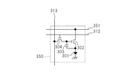
図10は、第3の実施形態における表示装置の各画素を概略的に示す図である。図10に示すように、各画素350は、有機EL素子301を有する。有機EL素子301の一端は、共通カソード電極に接地され、他端は、駆動TFT302を介して電源線351に接続される。
[Third embodiment]
FIG. 10 is a diagram schematically illustrating each pixel of the display device according to the third embodiment. As shown in FIG. 10, each
駆動TFT302のゲートソース間には、保持容量303が設けられる。駆動TFT302のゲートは、ゲートスイッチ304を介して、信号線313に接続される。ゲートスイッチ304のゲートは、ゲート走査線312に接続される。
A
なお、ゲートスイッチ304及び駆動TFT302は、サイズ以外は同一の基本構造を有するnチャネルのアモルファスSi−TFTで構成してもよいし、上記各画素350は、ガラス基板上に設けてもよい。また、図10に示す各画素350の基本的な動作は、第1の実施の形態と同様であるため、説明を省略する。
Note that the
図11は、第3の実施形態における駆動回路の概略を示す図である。図11では、説明の簡略化のために6×3ドットの画素350のみを示しているが、必要に応じて異なる画素数が用いられることはいうまでもない。また、表示単位である横方向3ドットの画素には、それぞれ赤(R)、緑(G)、青(B)の三色の有機EL素子301が設けられてもよい。
FIG. 11 is a diagram showing an outline of a drive circuit in the third embodiment. In FIG. 11, only the 6 × 3
図11に示すように、各画素350には、水平方向にゲート走査線312および電源線351が共通に接続される。ゲート走査線312の一端は、垂直走査回路354に接続される。電源線351の一端は、電源走査回路352に接続される。
As shown in FIG. 11, a
信号線313は、対応するRGBの発光色別に、切替えスイッチ321、322、323を介して、ドライバIC356に接続される。切替えスイッチ321、322、323のゲート走査線324、325、326及び垂直走査回路354の制御線群355、電源走査回路352の制御線群353は、ドライバIC356に接続される。
The
ドライバIC356は、第1の実施形態と同様、信号電圧Vsig、高電圧VH、低電圧VLを、各信号出力端子に選択的に出力する。同様に、例えば、信号電圧Vsigは0〜5V、高電圧VHは7V、低電圧VLは0Vの値を有するが、例えば、高電圧VHは7V以上の値に、低電圧VLは0V以下の値に設計してもよいことはいうまでもない。なお、この場合、ドライバIC356の耐圧設計はより複雑になるが、駆動TFT302の安定性をより向上させることができる。
As in the first embodiment, the
電源走査回路352は、後述するように、例えば、9V(Voled)、0Vの電圧を、スイッチ(図示せず)により、選択的に出力する。なお、各スイッチ321等及び垂直走査回路354は、サイズ以外は同一の基本構造を有するnチャネルのアモルファスSi−TFTで構成してもよいし、画素350と同一のガラス基板上に設けてもよい。また、ドライバIC356と電源走査回路352は,Si半導体チップで形成し、上記ガラス基板上にCOG(Chip-on Glass)実装してもよい。
As will be described later, the power
図12は、第3の実施形態における駆動回路の動作タイミング図である。図12において、横方向は、時間軸を示し、ここでは1水平走査期間(1H)を示している。Vsigは、ドライバIC356における信号線313の出力電圧、VHはドライバIC356における高電圧出力、VLはドライバIC356における低電圧出力、324、325、326はゲート走査線324、325、326に対応し、それぞれ上がオン、下がオフである。なお、Vsig、VH、VL、324、325、326は1H毎に繰返す信号である。
FIG. 12 is an operation timing chart of the drive circuit according to the third embodiment. In FIG. 12, the horizontal direction indicates the time axis, and here indicates one horizontal scanning period (1H). Vsig corresponds to the output voltage of the
下半分のタイミング図は、図4に示すタイミングt1、t2、t3、t4に関するゲート走査線312及び電源線351の走査タイミングを示す。各タイミングt1、t2、t3、t4は、第1の実施形態と同様である。
The timing chart of the lower half shows the scanning timing of the
次に、図12に示す1H期間を、T1、T2、T3、T4の各期間に分けて順次説明する。 Next, the 1H period shown in FIG. 12 will be described in order, divided into T1, T2, T3, and T4 periods.
期間T1には、ドライバIC356からRGBの順に信号線313の出力電圧が出力され、これがゲート走査線324、325、326によって走査される切替えスイッチ321、322、323によって信号線313上に出力される。タイミングt1、t3、t4、において、ゲート走査線312はオフであり、電源線351には0Vが印加される。
In the period T1, the output voltage of the
期間T2にはタイミングt1に、ゲート走査線312がオンすることによって、当該画素のゲートスイッチ304がオンする。ここで、信号線313の出力電圧がある程度の発光信号を有するときは、駆動TFT302はオンし、電源線351の電圧である0Vが駆動TFT302を介して、有機EL素子301のアノードに書込まれる。よって、保持容量303の両端には表示電圧として、信号線313の出力電圧がそのまま書込まれる。
In the period T2, at the timing t1, the
一方、信号線313の出力電圧が殆んど発光信号を有さないときは、駆動TFT302はオンしないため、保持容量303の両端には、信号線313の出力電圧が有機EL素子301の端子間容量との容量分割で書込まれる。しかしながら、後述するように有機EL素子301のアノード電圧の初期値は0Vであり、また有機EL素子301の端子間容量は十分に大きいため、書込まれる表示電圧は、信号線313の出力電圧の90%程度の値となる。
On the other hand, when the output voltage of the
期間T3にはドライバIC356から電圧VH(7V)が出力され、当該電圧VHがゲート走査線324、325、326によって同時にオンされる切替えスイッチ321、322、323によって信号線313上に出力される。
In the period T3, a voltage VH (7 V) is output from the
タイミングt3においてゲート走査線312がオンすることによって、当該画素のゲートスイッチ304がオンする。よって、ゲートスイッチ304から、信号線313を介して、駆動TFT302のゲートにVH(7V)が書込まれる。したがって、駆動TFT302は、オンし、電源線351の電圧である例えば、0Vが、駆動TFT302を介して、有機EL素子301のアノードに書込まれる。よって保持容量303の両端には表示電圧に替えてVH(7V)がそのまま書込まれる。
When the
期間T4には、ドライバIC356から電圧VL(0V)が出力され、当該電圧VLがゲート走査線324、325、326によって同時にオンされる切替えスイッチ321、322、323によって,信号線313に出力される。タイミングt4においてゲート走査線312がオンするため、当該画素のゲートスイッチ304がオンする。よって、ゲートスイッチ304から信号線313を介して駆動TFT302のゲートにVL(0V)が書込まれるため,駆動TFT302はオフされる。したがって、保持容量303の両端にはVL(0V)が,有機EL素子301の端子間容量との容量分割で書込まれる。
In the period T4, the voltage VL (0 V) is output from the
このとき,有機EL素子301のアノードには,タイミングt3で既に0Vが書込まれており、また,有機EL素子301の端子間容量は十分に大きいため、VL(0V)が,ほぼそのまま保持容量303の両端に書込まれる。なお、前述のように、有機EL素子301のアノードの電圧はタイミングt1に至るまで、このままほぼ0Vを維持すると考えて良い。
At this time, 0 V has already been written to the anode of the
次に、次に、1フレーム期間の観点から、駆動回路の具体的な動作につき説明する。
タイミングt1からt3までの期間であって、タイミングt2に代表される期間A(有機EL素子301の発光期間)には、電源線351がオン(例えばVoled、9V)を出力)する。
Next, a specific operation of the drive circuit will be described from the viewpoint of one frame period.
In a period from timing t1 to t3 and represented by timing A2 (light emission period of the organic EL element 301), the
既に、タイミングt1において保持容量303の両端には表示電圧が書込まれ、この表示電圧が駆動TFT302のゲートソース間に印加される。よって、駆動TFT302は表示電圧に対応した電流で有機EL素子301を駆動し発光させる。なお、この期間Aは、例えば、1フレームの約半分程度である。
The display voltage is already written to both ends of the
次に、電源線351がオフ(0Vを出力)することによって発光期間が終了し、タイミングt3でストレス電圧VH(7V)が、駆動TFT302のゲートソース間に設けられた保持容量303に書込まれ、期間Bの間保持される。
Next, the light emission period ends when the
次に、タイミングt4で、緩和電圧VL(0V)が駆動TFT302のゲートソース間に設けられた保持容量303に書込まれ、期間Cの間保持される。その後、最初のタイミングt1に戻り新たな表示電圧が書込まれる。以上のような動作が、1フレーム期間毎に繰り返し行われる。
Next, the relaxation voltage VL (0 V) is written into the
上記のように、本実施の形態によれば、画素350の回路を2つのTFTで構成することが可能であることから、高精細化に有利であり、また、歩留りの向上にも極めて有利である。また、大型パネルを製造する際には、TFTの歩留りが非常に重要となるため、本実施の形態の表示装置は、大形パネルに効果的に適用することができる。なお、その場合には、各ゲート線や信号線の負荷容量が大きくなる場合があり得る。したがって、駆動能力を確保するため、上記垂直走査回路354もICチップで構成することが望ましく、また、切替えスイッチ321、322、323を設けない方が望ましい。
As described above, according to the present embodiment, the circuit of the
また、第1の実施形態と同様、本実施の形態によれば、ストレス電圧の印加により、駆動TFT302の特性変化に起因する焼付きを解消することができる。また、緩和電圧の印加期間を設けることにより、ストレス電圧による駆動TFT302の過剰な特性変化を回復させることができる。結果として、長期間に渡る安定した輝度での画像表示が可能となる。いいかえれば、ストレス電圧印加による駆動TFT302のより大きい特性変動に対して均一に特性変動を回復することができ、駆動回路に起因する焼付きや輝度低下を生じない表示装置を実現することができる。
Further, as in the first embodiment, according to the present embodiment, it is possible to eliminate the image sticking caused by the characteristic change of the driving
[第4の実施形態]
図13は、第4の実施形態における表示装置の各画素を概略的に示す図である。図13に示すように、各画素360は、有機EL素子301を有する。有機EL素子301の一端は、共通カソード電極に接地され、他端は、駆動TFT302と発光制御スイッチ306を介して、電源線314に接続される。
[Fourth Embodiment]
FIG. 13 is a diagram schematically illustrating each pixel of the display device according to the fourth embodiment. As shown in FIG. 13, each
駆動TFT302のゲートソース間には、保持容量303を設ける。駆動TFT302のゲートは、ゲートスイッチ304を介して、信号線313に接続され、駆動TFT302のドレインは、チャネルスイッチ307を介して、低電圧線315に接続される。また、駆動TFT302のゲートは、第2ゲートスイッチ361を介して、電源線314に接続され、駆動TFT302のドレインは、第2チャネルスイッチ362を介して、低電圧線315に接続される。
A
発光制御スイッチ306のゲートは、発光制御線311に接続され、ゲートスイッチ304及びチャネルスイッチ307のゲートは、ゲート走査線312に接続される。第2ゲートスイッチ361及び第2チャネルスイッチ362のゲートは、第2ゲート走査線363に接続される。
The gate of the light
なお、各スイッチ321等及び駆動TFT302は、そのサイズ以外は同一の基本構造を有するnチャネルのアモルファスSi−TFTで構成してもよいし、各画素360はガラス基板上に設けてもよい。また、図13に示す各画素の基本的な動作は、第1の実施の形態と同様であるため、説明を省略する。
The
図14は、第4の実施形態における駆動回路の概略を示す図である。図14では、説明の簡略化のために6×3ドットの画素360のみを示しているが、必要に応じて異なる画素数が用いられることはいうまでもない。
FIG. 14 is a diagram schematically illustrating a drive circuit according to the fourth embodiment. In FIG. 14, only the 6 × 3
図14に示すように、画素360には、水平方向に、発光制御線311およびゲート走査線312、第2ゲート走査線363が接続される。また、発光制御線311およびゲート走査線312、第2ゲート走査線363の一端は、垂直走査回路365に接続される。
As shown in FIG. 14, the light
電源線314と低電圧線315は、それぞれ一端で電源入力線327と低電圧線入力線328に接続され、例えば、それぞれ10Vと0Vが外部より入力される。信号線313は、対応するRGBの発光色別に切替えスイッチ321、322、323を介してドライバIC364に接続される。
The
切替えスイッチ321、322、323のゲート走査線324、325、326及び垂直走査回路365の制御線群366はドライバIC364に接続される。ドライバIC364は、信号電圧Vsig、低電圧VLを、スイッチ702を介して、各信号出力端子に選択的に出力する。なお、例えば、信号電圧Vsigは0〜5V、低電圧VLは0Vの電圧値を有する。
The
なお、各切替えスイッチ321等及び垂直走査回路365は、サイズ以外は同一の基本構造を有するnチャネルのアモルファスSi−TFTで構成してもよい。また、画素360と同一のガラス基板上に設けてもよい。また、ドライバIC364はSi半導体チップで形成してもよく、上記ガラス基板上にCOG(Chip-On Glass)実装してもよい。
Each
図15は、第4の実施形態における駆動回路の動作タイミング図である。横方向は、時間軸を示し、ここでは1水平走査期間(1H)を示す。Vsigは、ドライバIC364における信号線313の出力電圧、VLはドライバIC364における低電圧出力、324、325、326はゲート走査線324、325、326に対応し、それぞれ上がオン、下がオフを示す。なお、Vsig、VL、324、325、326は1H毎に繰返す信号である。
FIG. 15 is an operation timing chart of the drive circuit according to the fourth embodiment. The horizontal direction represents a time axis, and here represents one horizontal scanning period (1H). Vsig corresponds to the output voltage of the
下半分のタイミング図は、図4のタイミングt1、t2、t3、t4に関する発光制御線311及びゲート走査線312、第2ゲート走査線363の走査タイミングをそれぞれ示す。ここでタイミングt1、t2、t3、t4とは、図4に示したt1、t2、t3、t4と同様であり、それぞれ時刻t1、t2、t3、t4における1列目の画素の動作と対応している。
The timing chart in the lower half shows scanning timings of the light
次に、1H期間を、図15に記載したようにT1、T2、T5の期間に分けて順次説明する。 Next, the 1H period will be described in order by dividing it into T1, T2, and T5 periods as shown in FIG.
期間T1には、ドライバIC364からRGBの順に信号線313の出力電圧が出力され、これがゲート走査線324、325、326によって走査される切替えスイッチ321、322、323によって信号線313上に出力される。この期間は、タイミングt1、t3、t4において、発光制御線311及びゲート走査線312、第2ゲート走査線363は共にオフである。
In the period T1, the output voltage of the
期間T2には、タイミングt1でゲート走査線312がオンすることによって、当該画素360のゲートスイッチ304及びチャネルスイッチ307がオンする。ここで、信号線313の出力電圧がある程度の発光信号を有するときは、駆動TFT302はオンし、低電圧線315の電圧である0Vが、チャネルスイッチ307と駆動TFT302を介して、有機EL素子301のアノードに書込まれる。よって、保持容量303の両端には表示電圧として、信号線313の出力電圧がそのまま書込まれる。
In the period T2, when the
一方、信号線313の出力電圧が殆んど発光信号を有さないときは、駆動TFT302はオンしないため、保持容量303の両端には信号線313の出力電圧が有機EL素子301の端子間容量との容量分割で書込まれる。しかし、後述するように有機EL素子301のアノード電圧の初期値は0Vであり、また有機EL素子301の端子間容量は十分に大きいため、書込まれる表示電圧は信号線313の出力電圧の90%程度の値となる。
On the other hand, when the output voltage of the
期間T5にはドライバIC364から電圧VL(0V)が出力され、当該電圧VLが、ゲート走査線324、325、326によって同時にオンされる切替えスイッチ321、322、323を介して、信号線313に出力される。
In the period T5, the voltage VL (0 V) is output from the
ここで、タイミングt3に相当する画素360においては、第2ゲート走査線363がオンすることによって、当該画素360の第2ゲートスイッチ361及び第2チャネルスイッチ362がオンする。このとき、電源線314から第2ゲートスイッチ361を介して駆動TFT302のゲートには、電源電圧(VH=Voled=10V)が書込まれるため、駆動TFT302はオンし、低電圧線315の電圧である0Vが第2チャネルスイッチ362と駆動TFT302を介して、有機EL素子301のアノードに書込まれる。よって、保持容量303の両端には表示電圧に替えて電源電圧(VH=Voled=10V)がそのまま書込まれる。
Here, in the
この水平走査タイミングにおいては同時に、タイミングt4に相当する画素において、ゲート走査線312がオンすることによって、当該画素のゲートスイッチ304及びチャネルスイッチ307がオンする。ここで、ゲートスイッチ304から、信号線313を介して、駆動TFT302のゲートには、VL(0V)が書込まれるため、駆動TFT302はオフされる。よって、保持容量303の両端には、VL(0V)が有機EL素子301の端子間容量との容量分割で書込まれる。
At the same time in the horizontal scanning timing, the
このとき、有機EL素子301のアノードにはタイミングt3で既に0Vが書込まれており、また、有機EL素子301の端子間容量は十分に大きいため、VL(0V)がほぼそのまま保持容量303の両端に書込まれる。なお、前述のように、有機EL素子301のアノードの電圧はタイミングt1に至るまで、このままほぼ0Vを維持すると考えて良い。
At this time, 0 V has already been written to the anode of the
次に、1フレーム期間の観点から、駆動回路の具体的な動作につき説明する。タイミングt2に代表される期間A(有機EL素子301の発光期間)には、発光制御線311がオンすることによって発光制御スイッチ306がオン状態に固定される。既にタイミングt1において保持容量303の両端には表示電圧が書込まれ、この表示電圧が駆動TFT302のゲートソース間に印加されるため、駆動TFT302は、表示電圧に対応した電流で有機EL素子301を駆動、発光させる。なお、この期間Aは、例えば、1フレームの約半分程度である。
Next, a specific operation of the drive circuit will be described from the viewpoint of one frame period. In the period A represented by the timing t2 (the light emission period of the organic EL element 301), the light
次に、発光制御線311がオフすることによって、発光制御スイッチ306がオフした後、タイミングt3でストレス電圧VH(=Voled=10V)が駆動TFT302のゲートソース間に設けられた保持容量303に書込まれ、期間Bの間保持される。
Next, when the light
次に、タイミングt4で緩和電圧VL(0V)が、駆動TFT302のゲートソース間に設けられた保持容量303に書込まれ、期間Cの間保持される。その後、1フレーム期間後に最初のタイミングt1に戻り新たな表示電圧が書込まれる。
Next, the relaxation voltage VL (0 V) is written into the
本実施の形態においては、ドライバIC364は、信号線313にストレス電圧VH(7V)を出力する必要がない。したがって、高電圧出力端子がTFT回路である切替えスイッチ321、322、323のゲート走査線324、325、326及び垂直走査回路365の制御線群366の駆動端子に限定される。結果として、ドライバIC364の大部分を低耐圧回路で構成でき、ドライバIC364の小型化と低コスト化が可能になる。また、ドライバIC364として既存の液晶ディスプレイ用ドライバIC341も流用することができ、コストを低減することができる。
In the present embodiment, the
また、第1の実施形態と同様、本実施の形態によれば、ストレス電圧の印加により、駆動TFT302の特性変化に起因する焼付きを解消することができる。また、緩和電圧の印加期間を設けることにより、ストレス電圧による駆動TFT302の過剰な特性変化を回復させることができる。結果として、長期間に渡る安定した輝度での画像表示が可能となる。いいかえれば、ストレス電圧印加による駆動TFT302のより大きい特性変動に対して均一に特性変動を回復することができ、駆動回路に起因する焼付きや輝度低下を生じない表示装置を実現することができる。
Further, as in the first embodiment, according to the present embodiment, it is possible to eliminate the image sticking caused by the characteristic change of the driving
[第5の実施形態]
図16は、第5の実施形態における表示装置の各画素を概略的に示す図である。図16に示すように、各画素370は、有機EL素子301を有する。当該有機EL素子301の一端は、共通カソード電極に接地され、他端は、駆動TFT302と発光制御スイッチ306を介して電源線314に接続される。
[Fifth Embodiment]
FIG. 16 is a diagram schematically illustrating each pixel of the display device according to the fifth embodiment. As shown in FIG. 16, each
駆動TFT302のゲートソース間には、保持容量303が設けられる。駆動TFT302のゲートは、ゲートスイッチ304を介して、信号線313に接続され、駆動TFT302のドレインは、チャネルスイッチ307を介して、低電圧線315に接続される。また、駆動TFT302のゲートは、ゲート電圧スイッチ71を介して、電圧制御373に接続され、駆動TFT302のドレインは、第2チャネルスイッチ362を介して低電圧線315に接続される。
A
発光制御スイッチ306のゲートは、発光制御線311に接続され、ゲートスイッチ304及びチャネルスイッチ307のゲートは、ゲート走査線312に接続される。また、ゲート電圧スイッチ371及び第2チャネルスイッチ362のゲートは、第3ゲート走査線372に接続される。
The gate of the light
なお、各スイッチ及び駆動TFT302は、そのサイズ以外は同一の基本構造を有するnチャネルのアモルファスSi−TFTで構成してもよい。また、各画素は、例えばガラス基板上に設けてもよい。また、図16に示す各画素370の基本的な動作は、第1の実施の形態と同様であるため、説明を省略する。
Each switch and the driving
図17は、第5の実施形態における駆動回路の概略を示す図である。図17は、説明の簡略化のため、6×3ドットの画素370を示しているが、必要に応じて異なる画素数が用いられることはいうまでもない。また、表示単位である横方向3ドットの画素370には、それぞれ赤(R)、緑(G)、青(B)の三色の有機EL素子301が設けられてもよい。
FIG. 17 is a diagram schematically illustrating a drive circuit according to the fifth embodiment. FIG. 17 shows a 6 × 3
図17に示すように、各画素370は、水平方向に、発光制御線311およびゲート走査線312、第3ゲート走査線372、電圧制御373が接続される。また、発光制御線311およびゲート走査線312、第3ゲート走査線372、電圧制御373の一端は、垂直走査回375に接続される。
As shown in FIG. 17, each
電源線314と低電圧線315は、それぞれ一端で電源入力線327と低電圧線入力線328に接続され、例えば、それぞれ10Vと0Vが外部より入力される。信号線313は、対応するRGBの発光色別に、切替えスイッチ321、322、323を介して、ドライバIC374に接続される。
The
切替えスイッチ321、322、323のゲートに接続されるゲート走査線324、325、326及び垂直走査回375の制御線群376は、ドライバIC374に接続される。ドライバIC374は、信号電圧Vsigを出力する。なお、例えば、信号電圧Vsigは0〜5Vの値である。
The
垂直走査回375は、電圧制御373に対して高電圧VH、低電圧VLを選択的に出力する。なお、例えば、高電圧VHは、7Vの電圧値を有し、低電圧VLは、0Vの電圧値を有する。
The
なお、各切替えススイッチ321等及び垂直走査回375は、サイズ以外は同一の基本構造を有するnチャネルのアモルファスSi−TFTで構成してもよい。また、画素370と同一のガラス基板上に設けてもよい。ドライバIC374は、Si半導体チップで構成してもよく、上記ガラス基板上にCOG(Chip-On Glass)実装してもよい。
Each switching
図18は、第5の実施形態における駆動回路の動作タイミング図である。横方向は、時間軸を示し、ここでは1水平走査期間(1H)を示す。Vsigは、ドライバIC374における信号線313の出力電圧、324、325、326はゲート走査線324、325、326に対応し、それぞれ上がオン、下がオフを示す。なお、Vsig、324、325、326は1H毎に繰返す信号である。
FIG. 18 is an operation timing chart of the drive circuit according to the fifth embodiment. The horizontal direction represents a time axis, and here represents one horizontal scanning period (1H). Vsig corresponds to the output voltage of the
下半分のタイミング図は、タイミングt1、t2、t3、t4に関する発光制御線311及びゲート走査線312、第3ゲート走査線372、電圧制御373の走査タイミングをそれぞれ示す。なお、タイミングt1、t2、t3、t4とは、図4に示したt1、t2、t3、t4と同様であり、それぞれ時刻t1、t2、t3、t4における1列目の画素の動作と対応している。
The timing chart of the lower half shows the scanning timing of the light
次に、上記1H期間を、T1、T6の期間に分けて順次説明する。 Next, the 1H period will be described in order by dividing it into periods T1 and T6.
期間T1には、ドライバIC374からRGBの順に信号線313の出力電圧が出力され、これがゲート走査線324、325、326によって走査される切替えスイッチ321、322、323によって信号線313に出力される。タイミングt1、t3、t4、において、発光制御線311及びゲート走査線312、第3ゲート走査線372は、共にオフである。また、電圧制御373には、VL(0V)が入力される。
In the period T1, the output voltage of the
期間T6には、タイミングt1に相当する画素370においては、ゲート走査線312がオンすることによって、当該画素のゲートスイッチ304及びチャネルスイッチ307がオンする。
In the period T6, in the
ここで、信号線313の出力電圧がある程度の発光信号を有するときは、駆動TFT302はオンし、低電圧線315の電圧である0Vがチャネルスイッチ307と駆動TFT302を介して、有機EL素子301のアノードに書込まれる。よって、保持容量303の両端には表示電圧として、信号線313の出力電圧がそのまま書込まれる。
Here, when the output voltage of the
一方、信号線313の出力電圧が殆んど発光信号を有さないときは、駆動TFT302は、オンしないため、保持容量303の両端には信号線313の出力電圧が有機EL素子301の端子間容量との容量分割で書込まれる。しかし、後述するように、有機EL素子301のアノード電圧の初期値は0Vであり、また、有機EL素子301の端子間容量は十分に大きいため、書込まれる表示電圧は信号線313の出力電圧の90%程度の値となる。
On the other hand, when the output voltage of the
また、同じT6の期間に、タイミングt3に相当する画素においては、第3ゲート走査線372がオンすることによって、当該画素のゲート電圧スイッチ371及び第2チャネルスイッチ362がオンする。ここで、同時に、電圧制御373にはVH(7V)が印加されており、電圧制御373からゲート電圧スイッチ371を介して、駆動TFT302のゲートにはVH(7V)が書込まれる。よって、駆動TFT302はオンし、低電圧線315の電圧である0Vが、第2チャネルスイッチ362と駆動TFT302を介して有機EL素子301のアノードに書込まれる。したがって、保持容量303の両端には表示電圧に替えてVH(7V)がそのまま書込まれる。
In the same T6 period, in the pixel corresponding to the timing t3, the third
更に、同じT6の期間に、タイミングt4に相当する画素においては、第3ゲート走査線372がオンすることによって、当該画素のゲート電圧スイッチ371及び第2チャネルスイッチ362がオンする。ここで、同時に、電圧制御373にはVL(0V)が印加されており、電圧制御373からゲート電圧スイッチ371を介して駆動TFT302のゲートにはVL(0V)が書込まれる。よって、駆動TFT302はオフし、保持容量303の両端にはVL(0V)が有機EL素子301の端子間容量との容量分割で書込まれる。
Further, in the same period T6, in the pixel corresponding to the timing t4, the third
このとき、有機EL素子301のアノードにはタイミングt3で既に0Vが書込まれており、また有機EL素子301の端子間容量は十分に大きいため、VL(0V)がほぼそのまま保持容量303の両端に書込まれる。なお、前述のように、有機EL素子301のアノードの電圧はタイミングt1に至るまで、このままほぼ0Vを維持すると考えて良い。
At this time, 0V has already been written to the anode of the
次に、1フレーム期間の観点から、駆動回路の具体的な動作につき説明する。タイミングt2に代表される期間A(有機EL素子301の発光期間)には、発光制御線311がオンすることにより、発光制御スイッチ306がオン状態に固定される。既にタイミングt1において保持容量303の両端には表示電圧が書込まれており、この表示電圧が駆動TFT302のゲートソース間に印加されるため、駆動TFT302は、表示電圧に対応した電流で有機EL素子301を駆動、発光させる。なお、この期間Aは、例えば、1フレームの約半分程度である。
Next, a specific operation of the drive circuit will be described from the viewpoint of one frame period. In the period A represented by the timing t2 (the light emission period of the organic EL element 301), the light
次に、この後発光制御線311がオフすることによって発光制御スイッチ306がオフした後、タイミングt3でストレス電圧VH(7V)が駆動TFT302のゲートソース間に設けられた保持容量303に書込まれ、期間Bの間保持される。
Next, after the light
次に、タイミングt4で緩和電圧VL(0V)が駆動TFT302のゲートソース間に設けられた保持容量303に書込まれ、期間Cの間保持される。次に、最初のタイミングt1に戻り新たな表示電圧が書込まれる。上記のような動作が、1フレーム期間毎に繰り返される。
Next, the relaxation voltage VL (0 V) is written into the
本実施の形態によれば、図18に示したように、1H期間における走査線駆動シーケンスが簡単にすることができる。したがって、本実施の形態によれば、1H期間の短い高精細の表示装置や、大型で走査線等の駆動容量が大きいため複雑な走査を行いにくい表示装置を容易に実現することができる。 According to this embodiment, as shown in FIG. 18, the scanning line driving sequence in the 1H period can be simplified. Therefore, according to this embodiment, a high-definition display device having a short 1H period or a display device that is large and has a large drive capacity such as a scanning line can be easily realized.
また、第4の実施形態と同様、ドライバIC374は信号線313にストレス電圧VH(7V)を出力する必要がない。したがって、高電圧出力端子がTFT回路である切替えスイッチ321、322、323のゲート走査線324、325、326及び垂直走査回路365の制御線群366の駆動端子に限定することができる。よって、ドライバIC374の大部分を低耐圧回路で構成することができ、結果として、ドライバIC374の小型化と低コスト化が可能となる。更に、ドライバIC374に、例えば既存の液晶ディスプレイに使用するドライバICを流用することができ、コストを低減することができる。
Further, as in the fourth embodiment, the
また、第1の実施形態と同様、本実施の形態によれば、ストレス電圧の印加により、駆動TFT302の特性変化に起因する焼付きを解消することができる。また、緩和電圧の印加期間を設けることにより、ストレス電圧による駆動TFT302の過剰な特性変化を回復させることができる。結果として、長期間に渡る安定した輝度での画像表示が可能となる。いいかえれば、ストレス電圧印加による駆動TFT302のより大きい特性変動に対して均一に特性変動を回復することができ、駆動回路に起因する焼付きや輝度低下を生じない表示装置を実現することができる。
Further, as in the first embodiment, according to the present embodiment, it is possible to eliminate the image sticking caused by the characteristic change of the driving
[第6の実施形態]
図19は、第6の実施形態における表示装置の各画素の配置を概略的に示す図である。第6の実施形態においては、低電圧線の構成が、第1の実施形態と異なる。その他の点は、上記第1の実施形態と同様であり、同様である点については説明を省略する。また、図19においては、説明の簡略化のために横4ドット、縦2ドットの計8個分の画素380のみを示しているが、必要に応じて、異なる画素数が用いられることはいうまでもない。
[Sixth Embodiment]
FIG. 19 is a diagram schematically showing the arrangement of each pixel of the display device according to the sixth embodiment. In the sixth embodiment, the configuration of the low voltage line is different from that of the first embodiment. Other points are the same as those in the first embodiment, and the description of the same points is omitted. Further, in FIG. 19, for simplification of explanation, only a total of eight
図19に示すように、各画素380は、歩留の向上を目的としたレイアウトの簡略化のために、電源線314、低電圧線381を左右の画素380間で共有する。具体的には、低電圧線381は、隣接する画素380間で相互接続され、有機EL素子301の共通のカソード接地電極に接続される。
As shown in FIG. 19, each
ここで、例えば、40型を超えるTVのような表示装置においては、有機EL素子301の共通カソード接地電極を透明電極で形成すると、抵抗が大きくなりすぎる。そこで、本実施の形態においては、有機EL素子301の共通のカソード接地電極を、例えば、厚さ200nmの金属Al薄膜で形成し、いわゆるボトムエミッション構造とする。これにより、共通のカソード接地電極の抵抗を十分低く抑えることができ、画素部にコンタクトホールを形成し、低電圧線381を共通のカソード接地電極に接続することができる。
Here, for example, in a display device such as a TV over 40 type, when the common cathode ground electrode of the
よって、本実施の形態においては、低電圧線381を画素マトリクス内に延長する必要がない。したがって、画素380のレイアウトを簡略化することができる。また、電圧降下を回避するために太い配線が必要である低電圧線入力線328を設ける必要がないため、額縁領域を縮小することができる。
Therefore, in this embodiment mode, it is not necessary to extend the
また、本実施の形態によれば、第1の実施形態と同様、ストレス電圧の印加により、駆動TFT302の特性変化に起因する焼付きを解消することができる。また、緩和電圧の印加期間を設けることにより、ストレス電圧による駆動TFT302の過剰な特性変化を回復させることができる。結果として、長期間に渡る安定した輝度での画像表示が可能となる。いいかえれば、ストレス電圧印加による駆動TFT302のより大きい特性変動に対して均一に特性変動を回復することができ、駆動回路に起因する焼付きや輝度低下を生じない表示装置を実現することができる。
Further, according to the present embodiment, as in the first embodiment, the image sticking caused by the characteristic change of the driving
なお、本実施の形態においては、上述のように、低電圧線381を共通のカソード接地電極に接続する手法を、ボトムエミッション構造と組み合わせたが、必要であればトップエミッション構造との組合せも可能であることはいうまでもない。
In the present embodiment, as described above, the method of connecting the
[第7の実施形態]
図20は、本発明の第7の実施形態における表示装置の各画素の配置を概略的に示す図である。第7の実施形態においては、画素の構成が一部において、第1の実施形態と異なる。その他の点は、上記第1の実施形態と同様であり、同様である点については説明を省略する。
[Seventh Embodiment]
FIG. 20 is a diagram schematically showing the arrangement of each pixel of the display device according to the seventh embodiment of the present invention. In the seventh embodiment, the configuration of the pixels is partially different from that of the first embodiment. Other points are the same as those in the first embodiment, and the description of the same points is omitted.
図20に示すように、各画素390は、有機EL素子301を有する。当該有機EL素子301の一端は、共通カソード電極に接地され、他端は、駆動TFT302と発光制御スイッチ306を介して、電源線314に接続される。
As shown in FIG. 20, each
駆動TFT302のゲートソース間には保持容量303が設けられる。駆動TFT302のゲートは、ゲートスイッチ304を介して、信号線313に接続される。駆動TFT302のソースは、ソーススイッチ391を介して、低電圧線315に接続される。発光制御スイッチ306のゲートは、発光制御線311に接続され、ゲートスイッチ304及びソーススイッチ391のゲートは、ゲート走査線312に接続される。駆動TFT302のドレインと電源線314間には、安定化容量392が設けられる。
A
なお、各スイッチ391等及び駆動TFT302は、そのサイズ以外は同一の基本構造を有するnチャネルのアモルファスSi−TFTで構成してもよいし、各画素390はガラス基板上に形成してもよい。
The
本実施の形態においては、チャネルスイッチ307に替わりにソーススイッチ391を設けるため、ソーススイッチ391から直接有機EL素子301のアノード電圧を制御することができる。この点、チャネルスイッチ307から駆動TFT302を介して有機EL素子301のアノード電圧を制御する第1の実施形態と異なる。従って、本実施の形態によれば、駆動TFT302のゲート電圧に関わらず有機EL素子301のアノード電圧を直接制御できる。よって、保持容量303の制御をより安定化させることができる。
In this embodiment, since the
第1の実施形態の場合には、駆動TFT302のソース端子には有機EL素子301の比較的大きな容量が接続されているため、駆動TFT302をオフしても駆動TFT302のソース端子の電圧は安定する。しかしながら、駆動TFT302のドレイン端子の電圧を、駆動TFT302を介して制御すると、特に、駆動TFT302のゲート電圧が低い場合には制御性が悪くなる場合がある。つまり、発光制御スイッチ306がオフ時に駆動TFT302をオフすると、駆動TFT302のドレイン端子の電圧は、安定しにくい。
In the case of the first embodiment, since a relatively large capacitance of the
そこで、本実施の形態では、駆動TFT302のソース端子に、新たに安定化容量392を設ける。よって、駆動TFT302のドレイン端子電圧を安定化することができる。具体的には、駆動TFT302のドレイン端子電圧は、駆動TFT302のゲート電圧の変位に対して、ドレインゲート間カップリング容量と安定化容量392の比率によって安定化することができる。
Therefore, in this embodiment, a
また、本実施の形態によれば、第1の実施形態と同様、ストレス電圧の印加により、駆動TFT302の特性変化に起因する焼付きを解消することができる。また、緩和電圧の印加期間を設けることにより、ストレス電圧による駆動TFT302の過剰な特性変化を回復させることができる。結果として、長期間に渡る安定した輝度での画像表示が可能となる。いいかえれば、ストレス電圧印加による駆動TFT302のより大きい特性変動に対して均一に特性変動を回復することができ、駆動回路に起因する焼付きや輝度低下を生じない表示装置を実現することができる。
Further, according to the present embodiment, as in the first embodiment, the image sticking caused by the characteristic change of the driving
[第8の実施形態]
図21は、本発明の第8の実施形態における表示装置の各画素を概略的に示す図である。第8の実施形態においては、画素の構成が一部において、第1の実施形態と異なる。その他の点は、上記第1の実施形態と同様であり、同様である点については説明を省略する。
[Eighth embodiment]
FIG. 21 is a diagram schematically showing each pixel of the display device according to the eighth embodiment of the present invention. In the eighth embodiment, the configuration of the pixels is partly different from the first embodiment. Other points are the same as those in the first embodiment, and the description of the same points is omitted.
図21に示すように、各画素400は、有機EL素子301を有する。当該有機EL素子301の一端は、共通カソード電極に接地され、他端は、駆動TFT302と発光制御スイッチ306を介して、電源線314に接続される。
As shown in FIG. 21, each
駆動TFT302のゲートソース間には保持容量303が設けられる。駆動TFT302のゲートは、ゲートスイッチ304を介して、信号線313に接続され、駆動TFT302のドレインは、チャネルスイッチ307を介して、低電圧線315に接続される。駆動TFT302のソースは、ソーススイッチ391を介して、低電圧線315に接続される。
A
発光制御スイッチ306のゲートは、発光制御線311によって、ゲートスイッチ304及びチャネルスイッチ307に接続される。ソーススイッチ391のゲートは、ゲート走査線312に接続される。なお、各スイッチ及び駆動TFT302は、そのサイズ以外は同一の基本構造を有するnチャネルのアモルファスSi−TFTで構成してもよいし、各画素400は、ガラス基板上に設けてもよい。
The gate of the light
また、本実施の形態においては、ソーススイッチ391を更に設けたため、第1の実施形態同様のチャネルスイッチ307から駆動TFT302のドレイン電圧を制御する機能と、ソーススイッチ391から直接有機EL素子301のアノード電圧を制御する機能を共に有する。従って、本実施の形態よれば、スイッチの数は増加するが、保持容量303の制御、及び、駆動TFT302のドレイン端子の制御を共に安定化させることができる。よって、動作マージンを格段に向上することができ、扱いやすい表示装置を提供することが可能である。
Further, in this embodiment, since the
また、本実施の形態によれば、第1の実施形態と同様、ストレス電圧の印加により、駆動TFT302の特性変化に起因する焼付きを解消することができる。また、緩和電圧の印加期間を設けることにより、ストレス電圧による駆動TFT302の過剰な特性変化を回復させることができる。結果として、長期間に渡る安定した輝度での画像表示が可能となる。いいかえれば、ストレス電圧印加による駆動TFT302のより大きい特性変動に対して均一に特性変動を回復することができ、駆動回路に起因する焼付きや輝度低下を生じない表示装置を実現することができる。
Further, according to the present embodiment, as in the first embodiment, the image sticking caused by the characteristic change of the driving
[第9の実施形態]
図22は、本発明の第9の実施形態における表示装置の各画素を概略的に示す図である。図22に示すように、各画素410は有機EL素子301を有する。当該有機EL素子301の一端は、共通カソード電極に接地され、他端は、発光制御スイッチ411と駆動TFT412を介して、電源線314に接続される。
[Ninth Embodiment]
FIG. 22 is a diagram schematically showing each pixel of the display device according to the ninth embodiment of the present invention. As shown in FIG. 22, each
駆動TFT412のゲートソース間には、保持容量303が設けられる。駆動TFT412のゲートは、ゲートスイッチ413を介して、信号線313に接続される。発光制御スイッチ411のゲートは、発光制御線311に接続される。ゲートスイッチ413のゲートは、ゲート走査線414に接続される。
A
なお、各スイッチ及び駆動TFT412は、そのサイズ以外は同一の基本構造を有するpチャネルの微結晶Si−TFTで構成してもよいし、各画素410は、ガラス基板上に形成してもよい。また、第9の実施形態の動作は、第1の実施形態の動作と基本的に同様であるが、第9の実施形態においては、後述するように、駆動TFT412がpMOSであるため、ゲートへ印加するストレス電圧及び緩和電圧は、第1の実施の形態と逆となることはいうまでもない。
Note that each switch and the driving
図23は、第9の実施形態における駆動回路の概略を示す図である。図23においては、図面の簡略化のため、6×3ドットの画素410のみを示しているが、必要に応じて異なる画素数が用いられることはいうまでもない。また、表示単位である横方向3ドットの画素410にはそれぞれ赤(R)、緑(G)、青(B)の3色の有機EL素子301を設けてもよい。なお、画素410は、第1の実施形態とは異なり、線対称レイアウトは採用していない。
FIG. 23 is a diagram schematically illustrating a drive circuit according to the ninth embodiment. In FIG. 23, for simplification of the drawing, only the 6 × 3
図23に示すように、各画素410には、水平方向に、発光制御線415およびゲート走査線414が接続され、これらの一端は、垂直走査IC417に接続される。電源線314は、一端が電源入力線327に接続され、例えば、10Vが外部より入力される。信号線313は、直接ドライバIC416に接続される。また、垂直走査IC417の制御線群418もドライバIC416に接続される。
As shown in FIG. 23, a light
ドライバIC416は、信号電圧Vsig、低電圧VL、高電圧VHを各信号出力端子に選択的に出力する。なお、例えば、信号電圧Vsigは5〜10V、低電圧VLは0V、高電圧VH10Vである。また、垂直走査IC417、及びドライバIC416はSi半導体チップで形成してもよく、ガラス基板上にCOG(Chip-On Glass)実装してもよい。
The
図24は、第9の実施形態における駆動回路の動作タイミング図である。横方向は、時間軸を示し、ここでは1水平走査期間(1H)を示す。Vsig(RGB別に3種類の信号が存在する)は、ドライバIC416における信号線313の出力電圧、VHは、ドライバIC416における高電圧出力、VLはドライバIC416における低電圧出力に対応し、それぞれ上がオン、下がオフである。なお、Vsig、VH、VLは1H毎に繰返す信号である。
FIG. 24 is an operation timing chart of the drive circuit according to the ninth embodiment. The horizontal direction represents a time axis, and here represents one horizontal scanning period (1H). Vsig (there are three types of signals for each RGB) corresponds to the output voltage of the
下半分のタイミング図は、タイミングt1、t2、t3、t4に関するゲート走査線414および発光制御線415の走査タイミングを示す。ここで、タイミングt1、t2、t3、t4とは、図4に示したt1、t2、t3、t4と同様であり、それぞれ時刻t1、t2、t3、t4における第1列目の画素の動作と対応している。
The timing chart in the lower half shows the scanning timing of the
次に、上記1H期間をT7、T8、T9の期間に分けて順次説明する。 Next, the 1H period will be described in order by dividing it into T7, T8, and T9 periods.
期間T7には、ドライバIC416から信号線313の出力電圧が、信号線313に出力される。タイミングt1においてゲート走査線414がオンすることによって、当該画素のゲートスイッチ413がオンする。このとき、信号線313の出力電圧は、保持容量303の一端にそのまま書込まれる。その後、ゲート走査線414がオフすることによって、信号線313の出力電圧は、保持容量303に出力される。なお、タイミングt3、t4においては、ゲート走査線414および発光制御線415はオフである。
In the period T <b> 7, the output voltage of the
期間T8には、ドライバIC416から電圧VL(0V)が出力され、当該電圧VLが信号線313に出力される。ここで、タイミングt3においては、ゲート走査線414がオンすることによって、当該画素のゲートスイッチ413がオンする。このとき、電圧VL(0V)は、保持容量303の一端にそのまま書込まれる。その後、ゲート走査線414がオフすることによって、電圧VL(0V)が、保持容量303に、出力される。なお、t1、t4においてはゲート走査線414および発光制御線415はオフである。
In the period T8, the
期間T9には、ドライバIC416から電圧VH(10V)が出力され、当該電圧VHが信号線313に出力される。ここで、タイミングt4においてはゲート走査線414がオンすることによって、当該画素のゲートスイッチ413がオンする。このとき、電圧VH(10V)は、保持容量303の一端にそのまま書込まれる。その後、ゲート走査線414がオフすることによって、電圧VH(10V)が保持容量303に出力される。なおt1、t3においてはゲート走査線414および発光制御線415はオフである。
In the period T <b> 9, the
次に、1フレーム期間の観点から、駆動回路の具体的な動作につき説明する。タイミングt2に代表される期間A(有機EL素子301の発光期間)には、発光制御線415がオンすることにより、発光制御スイッチ411がオン状態に固定される。既にタイミングt1において保持容量303の両端には表示電圧が書込まれており、この表示電圧が駆動TFT412のゲートソース間に印加されるため、駆動TFT412は、表示電圧に対応した電流で有機EL素子301を駆動し発光させる。なお、この期間Aは、例えば、1フレームの約半分程度である。
Next, a specific operation of the drive circuit will be described from the viewpoint of one frame period. In the period A represented by the timing t2 (the light emission period of the organic EL element 301), the light
次に、この発光制御線415がオフすることによって発光制御スイッチ411がオフした後、タイミングt3でストレス電圧VL(0V)が駆動TFT412のゲートソース間に設けられた保持容量303に書込まれ、期間Bの間保持される。次に、タイミングt4で緩和電圧VH(10V)が、駆動TFT412のゲートソース間に設けられた保持容量303に書込まれ、期間Cの間保持される。その後、最初のタイミングt1に戻り新たな表示電圧が書込まれる。上記のような動作が1フレーム期間毎に繰り返される。
Next, after the light emission control switch 411 is turned off by turning off the light
本実施の形態によれば、TFTとしてpMOSトランジスタを用いることによって、画素回路の簡略化が可能であるため、高精細化や高歩留りの実現に有利である。また、垂直走査IC417、及びドライバIC416を用いることにより、画素410周辺にTFT回路を設ける必要がない。よって高歩留りを実現することができる。更に、pMOS-TFTを用いることにより、有機トランジスタのように高性能のnMOS−TFTが作りにくいTFTプロセスにも対応することができる。
According to this embodiment, since a pixel circuit can be simplified by using a pMOS transistor as a TFT, it is advantageous for realizing high definition and high yield. Further, by using the
また、本実施の形態によれば、第1の実施形態同様、ストレス電圧の印加により、駆動TFT302の特性変化に起因する焼付きを解消することができる。また、緩和電圧の印加期間を設けることにより、ストレス電圧による駆動TFT412の過剰な特性変化を回復させることができる。結果として、長期間に渡る安定した輝度での画像表示が可能となる。いいかえれば、ストレス電圧印加による駆動TFT412のより大きい特性変動に対して均一に特性変動を回復することができ、駆動回路に起因する焼付きや輝度低下を生じないディスプレイを実現することができる。
Further, according to the present embodiment, as in the first embodiment, the image sticking caused by the characteristic change of the driving
[第10の実施形態]
図25は、本発明の第10の実施形態における表示装置の各画素を概略的に示す図である。第10の実施形態においては、画素の構成が一部において、第9の実施形態と異なる。その他の点は、上記第9の実施形態と同様であり、同様である点については説明を省略する。
[Tenth embodiment]
FIG. 25 is a diagram schematically showing each pixel of the display device according to the tenth embodiment of the present invention. In the tenth embodiment, the configuration of the pixels is partially different from that of the ninth embodiment. Other points are the same as those of the ninth embodiment, and the description of the same points is omitted.
図25に示すように、各画素420は、有機EL素子301を有する。当該有機EL素子301の一端は、共通カソード電極に接地され、他端は、発光制御スイッチ411と駆動TFT412を介して電源線314に接続される。
As shown in FIG. 25, each
駆動TFT412のゲートソース間には保持容量303が設けられる。駆動TFT412のゲートは、ゲートスイッチ413を介して、信号線313に接続される。発光制御スイッチ411のゲートは、発光制御線415に接続される。ゲートスイッチ413のゲートは、ゲート走査線414に接続される。以上は、第9の実施形態と同様である。
A
しかしながら、第10の実施形態においては、更に、駆動TFT412のドレインと電源線314との間に、ゲート走査線414によって制御されるチャネルスイッチ421を設ける。なお、各スイッチ421等及び駆動TFT412は、そのサイズ以外は同一の基本構造を有するpチャネルの微結晶Si−TFTで構成してもよく、各画素420はガラス基板上に形成してもよい。
However, in the tenth embodiment, a channel switch 421 controlled by the
本実施の形態においては、ゲート走査線414がオンする際に同時にチャネルスイッチ421がオンする。よって、駆動TFT412に印加した緩和電圧がゲート-ドレイン間にも着実に印加されるため、より動作を安定させることができる。また、信号線313の出力電圧を保持容量303に書込む際にも、ゲートソース間のみならずゲートドレイン間電圧を着実に一定に保つことができるため、ゲートドレイン間の寄生容量によって生じる輝度階調の歪みを防止することができる。
In this embodiment, when the
また、本実施の形態によれば、第1の実施形態同様、ストレス電圧の印加により、駆動TFT302の特性変化に起因する焼付きを解消することができる。また、緩和電圧の印加期間を設けることにより、ストレス電圧による駆動TFT412の過剰な特性変化を回復させることができる。結果として、長期間に渡る安定した輝度での画像表示が可能となる。いいかえれば、ストレス電圧印加による駆動TFT412のより大きい特性変動に対して均一に特性変動を回復することができ、駆動回路に起因する焼付きや輝度低下を生じないディスプレイを実現することができる。
Further, according to the present embodiment, as in the first embodiment, the image sticking caused by the characteristic change of the driving
なお、以上の第1乃至第10の実施形態は、カソード端子が共通である有機EL素子301を前提として、nMOS−TFT回路、及びpMOS-TFT回路に関して説明した。しかしながら、アノード端子が共通である有機EL素子301を前提とするならば、上記のnMOS−TFTを用いた各実施形態はnMOSをpMOSと置換することで、また上記のpMOS-TFTを用いた各実施形態はpMOSをnMOSと置換することで、それぞれ適用が可能である。
In the first to tenth embodiments described above, the nMOS-TFT circuit and the pMOS-TFT circuit have been described on the premise of the
[第11の実施形態]
図26は、第11の実施の形態における画素の動作を説明するための図である。第11の実施形態においては、画素の動作シーケンスが、第1の実施形態と異なる。その他の点は、上記第1の実施形態と同様であり、同様である点については説明を省略する。
[Eleventh embodiment]
FIG. 26 is a diagram for explaining the operation of the pixel in the eleventh embodiment. In the eleventh embodiment, the pixel operation sequence is different from that of the first embodiment. Other points are the same as those in the first embodiment, and the description of the same points is omitted.
図26の横方向は、各画素の縦方向の配列(列、row)を示し、横方向に第1列目から最終列までの画素に対応する。縦方向は、各画素の時間軸(time)を示し、縦方向の長さが1フレーム期間(1/60秒)に相当する。 The horizontal direction in FIG. 26 indicates the vertical arrangement (column, row) of each pixel, and corresponds to the pixels from the first column to the last column in the horizontal direction. The vertical direction indicates the time axis of each pixel, and the length in the vertical direction corresponds to one frame period (1/60 seconds).
斜めに記載された実線は、各画素列の走査タイミングを示す。具体的には、実線430は、保持容量303への表示電圧の書込み、実線432は、保持容量303へのストレス電圧の書込み、実線433は、保持容量303への緩和電圧の書込みを示す。実線431は、発光制御スイッチ306がオンすることによる発光の開始を示し、発光は実線432で終了する。
The solid line shown diagonally indicates the scanning timing of each pixel column. Specifically, the
本実施の形態においては、実線430の示す保持容量303への表示電圧の書込みは、第1の実施形態と同様に線順次走査で行われるが、実線432の示す保持容量303へのストレス電圧の書込み、及び実線433の示す保持容量303への緩和電圧の書込みは、全画素で一括して行う。
In the present embodiment, writing of the display voltage to the
なお、第1の実施形態と同様、図26において、期間Aは、駆動TFT302による有機EL素子301の発光期間、期間Bは、駆動TFT302に対するストレス電圧印加期間、期間Cは、駆動TFT302に対する緩和電圧印加期間を示す。
As in the first embodiment, in FIG. 26, period A is a light emission period of the
図27(A)乃至(D)は、第11の実施形態における駆動回路の動作タイミング図である。横方向は、時間軸を示し、ここでは1水平走査期間(1H)を示す。Vsigは、ドライバIC330における信号線313の出力電圧、VHは、ドライバIC330における高電圧出力、VLは、ドライバIC330における低電圧出力、324、325、326はゲート走査線324、325、326に対応し、それぞれ上がオン、下がオフである。なお、Vsig、VH、VL、324、325、326は1H毎に繰返す信号である。
FIGS. 27A to 27D are operation timing diagrams of the drive circuit in the eleventh embodiment. The horizontal direction represents a time axis, and here represents one horizontal scanning period (1H). Vsig corresponds to the output voltage of the
ここで、図27(A)乃至(D)はそれぞれ、タイミングt11、t12、t13、t14における発光制御線311及びゲート走査線312の1H期間の走査タイミングを示す。ここで、タイミングt11、t12、t13、t14は、図26に示したt11、t12、t13、t14であり、それぞれ時刻t11、t12、t13、t14における1列目の画素420の動作と対応する。
Here, FIGS. 27A to 27D show scanning timings of the light
図27(A)は、タイミングt11における1H期間の走査タイミングを示す。期間T1には、ドライバIC330からRGBの順に信号線313の出力電圧が出力され、これがゲート走査線324、325、326によって走査される切替えスイッチ321、322、323によって信号線313に出力される。なお、この期間は発光制御線311及びゲート走査線312は共にオフである。
FIG. 27A shows the scanning timing of the 1H period at the timing t11. In the period T1, the output voltage of the
期間T2にはゲート走査線312がオンすることによって、当該画素のゲートスイッチ304及びチャネルスイッチ307がオンする。ここで、信号線313の出力電圧がある程度の発光信号を有するときは、駆動TFT302はオンし、低電圧線315の電圧である0Vが、チャネルスイッチ307と駆動TFT302を介して、有機EL素子301のアノードに書込まれる。よって、保持容量303の両端には表示電圧として、信号線313の出力電圧がそのまま書込まれる。
In the period T2, when the
一方、信号線313の出力電圧が殆んど発光信号を有さないときは、駆動TFT302はオンしないため、保持容量303の両端には、信号線313の出力電圧が有機EL素子301の端子間容量との容量分割で書込まれる。しかし、後述するように有機EL素子301のアノード電圧の初期値は0Vであり、また有機EL素子301の端子間容量は十分に大きいため、書込まれる表示電圧は信号線313の出力電圧の90%程度の値となる。
On the other hand, when the output voltage of the
図27(B)は、タイミングt12における1H期間の走査タイミングを示す。この期間T10には、発光制御線311が全画素420で一斉にオンすることによって、発光制御スイッチ306がオン状態に固定される。既にタイミングt11において保持容量303の両端には表示電圧が書込まれており、この表示電圧が駆動TFT302のゲートソース間に印加されるため、駆動TFT302は表示電圧に対応した電流で有機EL素子301を駆動し発光させる。
FIG. 27B shows the scanning timing of the 1H period at the timing t12. In this period T10, the light
なお、タイミングt12に始まる発光期間Aは、例えば1フレームの約半分程度続き、その後発光制御線311が全画素で一斉にオフして発光期間Aが終了する。
Note that the light emission period A starting at the timing t12 lasts, for example, about half of one frame, and then the light
図27(C)はタイミングt13における1H期間の走査タイミングを示す。この期間T11には、ドライバIC330から電圧VH(7V)が出力され、これがゲート走査線324、325、326によって同時にオンされる切替えスイッチ321、322、323を介して、信号線313に出力される。
FIG. 27C shows the scanning timing of the 1H period at the timing t13. During this period T11, the
ここで、ゲート走査線312が全画素420で一斉にオンすることによって、各画素420のゲートスイッチ304及びチャネルスイッチ307がオンする。ここで、ゲートスイッチ304から信号線313を介して、駆動TFT302のゲートにはVH(7V)が書込まれるため、駆動TFT302はオンする。よって、低電圧線315の電圧である0Vが、チャネルスイッチ307と駆動TFT302を介して、有機EL素子301のアノードに書込まれる。したがって、保持容量303の両端には表示電圧に替えてVH(7V)がそのまま書込まれる。
Here, when the
図27(D)は、タイミングt14における1H期間の走査タイミングを示す。期間T12には、ドライバIC330から電圧VL(0V)が出力され、これがゲート走査線324、325、326によって同時にオンされる切替えスイッチ321、322、323によって、信号線313に出力される。
FIG. 27D shows the scanning timing of the 1H period at the timing t14. In the period T12, the
タイミングt14において、ゲート走査線312がオンすることによって、当該画素のゲートスイッチ304及びチャネルスイッチ307がオンしている。よって、ゲートスイッチ304から信号線313を介して、駆動TFT302のゲートにVL(0V)が書込まれるため、駆動TFT302はオフする。したがって、保持容量303の両端にはVL(0V)が有機EL素子301の端子間容量との容量分割で書込まれる。
At timing t14, when the
このとき、有機EL素子301のアノードには、タイミングt13で既に0Vが書込まれており、また有機EL素子301の端子間容量は十分に大きいため、VL(0V)が、ほぼそのまま保持容量303の両端に書込まれる。そして、有機EL素子301のアノードの電圧はタイミングt11に至るまで、このままほぼ0Vを維持する。
At this time, 0 V has already been written to the anode of the
次に、1フレーム期間の観点から、駆動回路の具体的な動作につき説明する。タイミングt12で開始される期間A(有機EL素子301の発光期間)には、全画素420で、発光制御線311が一斉にオンすることによって、発光制御スイッチ306がオン状態に固定される。既に線順次の信号書込み期間である期間Dにおいて、保持容量303の両端には表示電圧が書込まれており、この表示電圧が駆動TFT302のゲートソース間に印加されるため、駆動TFT302は、表示電圧に対応した電流で有機EL素子301を駆動し発光させる。
Next, a specific operation of the drive circuit will be described from the viewpoint of one frame period. In the period A (the light emission period of the organic EL element 301) started at the timing t12, the light
次に、発光制御線311が一斉にオフすることによって、発光制御スイッチ306がオフした後、タイミングt13で一斉にストレス電圧VH(7V)が駆動TFT302のゲートソース間に設けられた保持容量303に書込まれ、期間Bの間保持される。
Next, when the light
次に、タイミングt14で一斉に緩和電圧VL(0V)が駆動TFT302のゲートソース間に設けられた保持容量303に書込まれ、期間Cの間保持される。その後最初のタイミングt11に戻り、新たな表示電圧が線順次走査で書込まれる。上記のような動作が1フレーム期間毎に繰り返される。
Next, the relaxation voltage VL (0 V) is simultaneously written to the
本実施の形態によれば、全画素の発光期間Aが時間的に揃うため、特にスムーズに動画を表示することができる。ここで、画像のガンマ特性を損なうことなく画面全体の輝度を調整するためには、発光期間Aの長さを制御することが有利である。この場合において、特に発光期間を短く制御する場合には、理想的なパルス駆動が実現できる結果として、動画表示の質を向上することができる。 According to the present embodiment, since the light emission periods A of all the pixels are aligned in time, a moving image can be displayed particularly smoothly. Here, in order to adjust the luminance of the entire screen without impairing the gamma characteristic of the image, it is advantageous to control the length of the light emission period A. In this case, particularly when the light emission period is controlled to be short, the quality of moving image display can be improved as a result of realizing ideal pulse driving.
また、本実施の形態によれば、第1の実施形態と同様、ストレス電圧の印加により、駆動TFT302の特性変化に起因する焼付きを解消することができる。また、緩和電圧の印加期間を設けることにより、ストレス電圧による駆動TFT302の過剰な特性変化を回復させることができる。結果として、長期間に渡る安定した輝度での画像表示が可能となる。いいかえれば、ストレス電圧印加による駆動TFT302のより大きい特性変動に対して均一に特性変動を回復することができ、駆動回路に起因する焼付きや輝度低下を生じない表示装置を実現することができる。
Further, according to the present embodiment, as in the first embodiment, the image sticking caused by the characteristic change of the driving
[第12の実施の形態]
図28は、第12の実施の形態におけるTV画像表示装置を示す図である。図28に示すように、TV画像表示装置440は、有機ELディスプレイ441を有する。当該有機ELディスプレイ441は、例えば、上記第1の実施の形態で説明した画素回路を含む駆動回路に対応するものとする。
[Twelfth embodiment]
FIG. 28 is a diagram illustrating a TV image display device according to the twelfth embodiment. As shown in FIG. 28, the TV
図28に示すように、TV画像表示装置440は、電源449、無線インターフェース(I/F)回路442、及び、それぞれデータバス448に接続されたI/O(Input/Output)回路443、マイクロプロセッサ(MPU)444、表示パネルコントローラ446、フレームメモリ447を有する。
As shown in FIG. 28, a TV
無線インターフェース(I/F)回路442は、地上波デジタル信号等を受信する。具体的には、例えば、無線インターフェース(I/F)回路442は、圧縮された画像データ等を外部から無線データとして受信する。また、無線インターフェース(I/F)回路442は、I/O(Input/Output)回路443を介して、上記圧縮された画像データ等をデータバス448に出力する。
The radio interface (I / F)
表示パネルコントローラ446は、有機ELディスプレイ441に接続される。電源449は、例えば、二次電池を有し、TV画像表示装置440全体を駆動する電力を供給する。
The
次に、第12の実施形態の動作について説明する。まず、無線I/F回路442は命令に応じて圧縮された画像データを外部から取り込み、この画像データをI/O回路443を介して、マイクロプロセッサ444及びフレームメモリ447に転送する。
Next, the operation of the twelfth embodiment will be described. First, the wireless I /
マイクロプロセッサ444は、ユーザからの命令操作を受けて、必要に応じてTV画像表示装置440全体を駆動し、圧縮された画像データのデコードや信号処理、情報表示を行う。なお、信号処理された画像データは、フレームメモリ447に一時的に蓄積されてもよい。
In response to a command operation from the user, the microprocessor 444 drives the entire TV
マイクロプロセッサ444が表示命令を出した場合には、その指示に従い、フレームメモリ447から表示パネルコントローラ446を介して、有機ELディスプレイ441に画像データが入力され、有機ELディスプレイ441は入力された画像データをリアルタイムで表示する。
When the microprocessor 444 issues a display command, image data is input from the
このとき表示パネルコントローラ446は、同時に画像を表示するために必要な所定のタイミングパルスを出力及び制御する。なお、有機ELディスプレイ441がこれらの信号を用いて、入力された画像データをリアルタイムで表示することに関しては、例えば第1の実施形態で説明したので、ここでは説明を省略する。
At this time, the
本実施の形態によれば、焼付きの生じない高画質表示が可能であり、かつ製造コストの大幅に削減されたTV画像表示装置440を提供することができる。
According to this embodiment, it is possible to provide a TV
また、本実施の形態によれば、第1の実施形態と同様、ストレス電圧の印加により、駆動TFT302の特性変化に起因する焼付きを解消することができる。また、緩和電圧の印加期間を設けることにより、ストレス電圧による駆動TFT302の過剰な特性変化を回復させることができる。結果として、長期間に渡る安定した輝度でのディスプレイ表示が可能となる。いいかえれば、ストレス電圧印加による駆動TFT302のより大きい特性変動に対して均一に特性変動を回復することができ、駆動回路に起因する焼付きや輝度低下を生じないディスプレイを実現することができる。
Further, according to the present embodiment, as in the first embodiment, the image sticking caused by the characteristic change of the driving
なお、本実施の形態では有機ELディスプレイ441として、第1の実施形態で説明した駆動回路を用いたが、その他の実施形態に示した画素回路や駆動回路を用いてもよいことはいうまでもない。この場合、表示パネルコントローラ446の出力するタイミングパルスには、若干の変更が必要になることはいうまでもない。
In this embodiment, the drive circuit described in the first embodiment is used as the
なお、本発明は、上記第1乃至12の実施形態に限定されるものではなく、種々の変形が可能である。例えば、第1乃至12の実施形態で示した構成と実質的に同一の構成、同一の作用効果を奏する構成又は同一の目的を達成することができる構成で置き換えることができる。例えば、各実施の形態における画素の構成等はその一例であって、これに限定されるものではなく、実質的に同一の構成、同一の作用効果を奏する構成又は同一の目的を達成することができる構成で置き換えることができる。 The present invention is not limited to the first to twelfth embodiments, and various modifications can be made. For example, it can be replaced with a configuration that is substantially the same as the configuration shown in the first to twelfth embodiments, a configuration that exhibits the same operational effects, or a configuration that can achieve the same purpose. For example, the configuration of the pixel in each embodiment is an example, and the configuration is not limited thereto, and substantially the same configuration, the configuration having the same operation effect, or the same purpose can be achieved. It can be replaced with a possible configuration.
201、301 有機EL素子、202、302、412 駆動TFT、203 容量、204、205 TFTスイッチ、301 有機EL素子、303 保持容量、304 ゲートスイッチ、307 チャネルスイッチ、310 画素、313 信号線、314 電源線、315 低電圧線、321、322、323 切替えスイッチ、324、325、326 ゲート走査線、327 電源入力線、328 低電圧線入力線、330 ドライバIC、331 垂直走査回路、440 TV画像表示装置、442 無線インターフェース回路、444 マイクロプロセッサ、446 表示パネルコントローラ、447 フレームメモリ、448 データバス、449 電源。
201, 301 Organic EL element, 202, 302, 412 Driving TFT, 203 Capacitor, 204, 205 TFT switch, 301 Organic EL element, 303 Holding capacitor, 304 Gate switch, 307 Channel switch, 310 Pixel, 313 Signal line, 314 Power supply Line, 315 low voltage line, 321, 322, 323 changeover switch, 324, 325, 326 gate scanning line, 327 power input line, 328 low voltage line input line, 330 driver IC, 331 vertical scanning circuit, 440 TV
Claims (28)
前記発光素子への駆動電流を制御する駆動トランジスタと、
階調値に対応する電圧が書き込まれ保持するとともに、前記駆動トランジスタのゲートソース間に前記階調値に対応する電圧に応じた表示電圧を印加するための保持容量と、をそれぞれ有する複数の画素と、
前記駆動トランジスタのゲートソース間に、前記表示電圧の取り得る値の範囲外の電圧値を有するストレス電圧を印加するストレス電圧印加手段と、を有することを特徴とする表示装置。 A light emitting element;
A drive transistor for controlling a drive current to the light emitting element;
A plurality of pixels each having a storage capacitor for writing and holding a voltage corresponding to the gradation value and applying a display voltage corresponding to the voltage corresponding to the gradation value between the gate and source of the driving transistor When,
A display device comprising: a stress voltage applying unit that applies a stress voltage having a voltage value outside a range of possible values of the display voltage between the gate and source of the driving transistor.
前記表示装置は、更に、前記駆動トランジスタのゲートソース間に、前記高電圧値を印加する場合には、前記高電圧値よりも低い電圧値を印加し、前記低電圧値を印加する場合には、前記低電圧値よりも高い電圧値を有する緩和電圧を印加する緩和電圧印加手段を有することを特徴とする請求項1記載の表示装置。 The stress voltage applying means has a high voltage value having a voltage value higher than an upper limit value range of the display voltage, or a voltage value lower than a lower limit value range of the display voltage. Applying one of the low voltage values
The display device further applies a voltage value lower than the high voltage value when applying the high voltage value between the gate and source of the drive transistor, and applies the low voltage value. 2. The display device according to claim 1, further comprising relaxation voltage applying means for applying a relaxation voltage having a voltage value higher than the low voltage value.
前記表示装置は、更に、
前記表示電圧を生成する表示電圧発生手段と、
前記表示電圧を前記各画素に入力する信号線と、
前記各発光素子に発光電力を供給する電源線と、を有し、
前記各画素は、更に、画素スイッチを有し、
前記駆動トランジスタは電界効果トランジスタであって、
前記保持容量は、前記駆動トランジスタのゲートソース間に配置され、
前記電界効果トランジスタのソースまたはドレインの一方は、前記電源線に、他方は前記発光素子に接続され、
前記電界効果トランジスタのゲートは、前記画素スイッチを介して、前記信号線に接続されることを特徴とする請求項2記載の表示装置。 The plurality of pixels are arranged in a matrix,
The display device further includes:
Display voltage generating means for generating the display voltage;
A signal line for inputting the display voltage to each pixel;
A power line for supplying light emission power to each of the light emitting elements,
Each of the pixels further includes a pixel switch,
The driving transistor is a field effect transistor,
The storage capacitor is disposed between the gate and source of the driving transistor,
One of the source or drain of the field effect transistor is connected to the power supply line, and the other is connected to the light emitting element,
The display device according to claim 2, wherein a gate of the field effect transistor is connected to the signal line through the pixel switch.
前記表示電圧発生手段は、前記表示電圧、前記ストレス入力電圧、または、前記緩和入力電圧を、前記選択スイッチを介して、選択的に出力することを特徴とする請求項7記載の表示装置。 The display voltage generating means further includes a selection switch,
The display device according to claim 7, wherein the display voltage generation unit selectively outputs the display voltage, the stress input voltage, or the relaxation input voltage via the selection switch.
前記表示電圧発生手段は、前記ストレス入力電圧、または、前記緩和入力電圧を、前記選択スイッチを介して、選択的に出力することを特徴とする請求項7記載の表示装置。 The display voltage generating means further includes a selection switch,
The display device according to claim 7, wherein the display voltage generation unit selectively outputs the stress input voltage or the relaxation input voltage via the selection switch.
前記ストレス入力電圧及び前記緩和入力電圧を、前記ストレス電圧線を介して、前記複数の画素へ入力することを特徴とする請求項6記載の表示装置。 The display device further includes a stress voltage line provided in a direction perpendicular to the signal line,
The display device according to claim 6, wherein the stress input voltage and the relaxation input voltage are input to the plurality of pixels through the stress voltage line.
前記電界効果トランジスタは、nMOSであり、
前記電界効果トランジスタのソース端子は、前記発光素子に接続され、ドレイン端子は、前記発光制御スイッチを介して、前記電源線に接続され、
前記ストレス電圧を前記保持容量に印加する際、前記発光制御スイッチは、オフ状態に固定されることを特徴とする請求項6記載の表示装置。 Each pixel further includes a light emission control switch,
The field effect transistor is an nMOS;
A source terminal of the field effect transistor is connected to the light emitting element, and a drain terminal is connected to the power line via the light emission control switch,
The display device according to claim 6, wherein when the stress voltage is applied to the storage capacitor, the light emission control switch is fixed in an off state.
前記電界効果トランジスタは、nMOSであり、
前記電界効果トランジスタのソース端子は、前記発光素子に接続され、ドレイン端子は、前記発光制御スイッチを介して、前記電源線に接続され、
前記緩和電圧を前記保持容量に印加する際、前記発光制御スイッチは、オフ状態に固定されることを特徴とする請求項6記載の表示装置。 Each pixel further includes a light emission control switch,
The field effect transistor is an nMOS;
A source terminal of the field effect transistor is connected to the light emitting element, and a drain terminal is connected to the power line via the light emission control switch,
The display device according to claim 6, wherein when the relaxation voltage is applied to the storage capacitor, the light emission control switch is fixed to an off state.
前記電界効果トランジスタは、nMOSであり、
前記電界効果トランジスタのソース端子は、前記発光素子に接続され、ドレイン端子は、前記発光制御スイッチを介して、前記電源線に接続され、
前記表示電圧を前記保持容量に印加する際、前記発光制御スイッチは、オフ状態に固定されることを特徴とする請求項6記載の表示装置。 Each pixel further includes a light emission control switch,
The field effect transistor is an nMOS;
A source terminal of the field effect transistor is connected to the light emitting element, and a drain terminal is connected to the power line via the light emission control switch,
The display device according to claim 6, wherein when the display voltage is applied to the storage capacitor, the light emission control switch is fixed to an off state.
前記電界効果トランジスタは、pMOSであり、
前記電界効果トランジスタのソース端子は、前記電源線に接続され、ドレイン端子は、前記発光制御スイッチを介して、前記発光素子に接続され、
前記ストレス電圧を前記保持容量に印加する際、前記発光制御スイッチは、オフ状態に固定されることを特徴とする請求項1記載の表示装置。 Each pixel further includes a light emission control switch,
The field effect transistor is a pMOS;
A source terminal of the field effect transistor is connected to the power line, and a drain terminal is connected to the light emitting element via the light emission control switch,
The display device according to claim 1, wherein when the stress voltage is applied to the storage capacitor, the light emission control switch is fixed in an off state.
前記電界効果トランジスタは、pMOSであり、
前記電界効果トランジスタのソース端子は、前記電源線に接続され、ドレイン端子は、前記発光制御スイッチを介して、前記発光素子に接続され、
前記緩和電圧を前記保持容量に印加する際、前記発光制御スイッチは、オフ状態に固定されることを特徴とする請求項1記載の表示装置。 Each pixel further includes a light emission control switch,
The field effect transistor is a pMOS;
A source terminal of the field effect transistor is connected to the power line, and a drain terminal is connected to the light emitting element via the light emission control switch,
The display device according to claim 1, wherein, when the relaxation voltage is applied to the storage capacitor, the light emission control switch is fixed to an off state.
前記電界効果トランジスタは、pMOSであり、
前記電界効果トランジスタのソース端子は、前記電源線に接続され、ドレイン端子は、前記発光制御スイッチを介して、前記発光素子に接続され、
前記表示電圧を前記保持容量に印加する際、前記発光制御スイッチは、オフ状態に固定されることを特徴とする請求項1記載の表示装置。 Each pixel further includes a light emission control switch,
The field effect transistor is a pMOS;
A source terminal of the field effect transistor is connected to the power line, and a drain terminal is connected to the light emitting element via the light emission control switch,
The display device according to claim 1, wherein when the display voltage is applied to the storage capacitor, the light emission control switch is fixed in an off state.
前記電界効果トランジスタのドレイン端子は、前記第1のチャネルスイッチを介して、前記低電圧配線に接続されることを特徴とする請求項6記載の表示装置。 Each of the pixels further includes a channel switch and a low voltage wiring to which a predetermined constant voltage is applied,
The display device according to claim 6, wherein a drain terminal of the field effect transistor is connected to the low-voltage wiring through the first channel switch.
前記複数の画素は、前記チャネルスイッチを介して、行毎に制御されることを特徴とする請求項18記載の表示装置。 The gate of the channel switch is connected in common with the gate of the pixel switch,
The display device according to claim 18, wherein the plurality of pixels are controlled for each row via the channel switch.
前記電界効果トランジスタのドレイン端子は、前記第1のチャネルスイッチを介して、前記低電圧配線に接続され、ソース端子は、前記第2のチャネルスイッチを介して、前記低電圧配線に接続されることを特徴とする請求項6記載の表示装置。 Each of the pixels further includes a first channel switch, a second channel switch, and a low voltage wiring to which a predetermined constant voltage is applied.
The drain terminal of the field effect transistor is connected to the low-voltage wiring through the first channel switch, and the source terminal is connected to the low-voltage wiring through the second channel switch. The display device according to claim 6.
前記複数の画素は、前記第1及び第2のチャネルスイッチを介して、行毎に制御されることを特徴とする請求項20記載の表示装置。 The gates of the first and second channel switches are connected in common with the gate of the pixel switch,
21. The display device according to claim 20, wherein the plurality of pixels are controlled for each row via the first and second channel switches.
前記低電圧配線は、前記各画素内で接地されることを特徴とする請求項18記載の表示装置。 A terminal of the light emitting element that is not connected to the field effect transistor is commonly grounded between adjacent pixels among the plurality of pixels.
The display device according to claim 18, wherein the low voltage wiring is grounded in each pixel.
前記電界効果トランジスタのドレイン端子は、前記電源線に接続され、
前記表示電圧が前記保持容量に印加される際、前記電源線の電圧を、前記発光素子の他端に印加される電圧と等しい電圧とすることを特徴とする請求項6記載の表示装置。 A source terminal of the field effect transistor is connected to one end of the light emitting element,
The drain terminal of the field effect transistor is connected to the power line,
The display device according to claim 6, wherein when the display voltage is applied to the storage capacitor, the voltage of the power supply line is set equal to a voltage applied to the other end of the light emitting element.
前記電界効果トランジスタのドレイン端子は、前記電源線に接続され、
前記ストレス電圧が前記保持容量に印加される際、前記電源線の電圧を、前記発光素子の他端に印加される電圧と等しい電圧とすることを特徴とする請求項6記載の表示装置。 A source terminal of the field effect transistor is connected to one end of the light emitting element,
The drain terminal of the field effect transistor is connected to the power line,
The display device according to claim 6, wherein when the stress voltage is applied to the storage capacitor, the voltage of the power supply line is equal to a voltage applied to the other end of the light emitting element.
前記電界効果トランジスタのドレイン端子は、前記電源線に接続され、
前記緩和電圧が前記保持容量に印加される際、前記電源線の電圧を、前記発光素子の他端に印加される電圧と等しい電圧とすることを特徴とする請求項6記載の表示装置。 A source terminal of the field effect transistor is connected to one end of the light emitting element,
The drain terminal of the field effect transistor is connected to the power line,
The display device according to claim 6, wherein when the relaxation voltage is applied to the storage capacitor, the voltage of the power supply line is set equal to a voltage applied to the other end of the light emitting element.
前記表示データから前記表示電圧を発生する表示電圧発生手段と、
前記表示装置を駆動する電力を供給する供給装置と、を有することを特徴とする請求項1記載の表示装置。 The display device further includes a memory for storing display data corresponding to the display voltage;
Display voltage generating means for generating the display voltage from the display data;
The display device according to claim 1, further comprising a supply device that supplies electric power for driving the display device.
Priority Applications (2)
| Application Number | Priority Date | Filing Date | Title |
|---|---|---|---|
| JP2010198307A JP2012058274A (en) | 2010-09-03 | 2010-09-03 | Display device |
| US13/222,315 US8803924B2 (en) | 2010-09-03 | 2011-08-31 | Display device |
Applications Claiming Priority (1)
| Application Number | Priority Date | Filing Date | Title |
|---|---|---|---|
| JP2010198307A JP2012058274A (en) | 2010-09-03 | 2010-09-03 | Display device |
Publications (2)
| Publication Number | Publication Date |
|---|---|
| JP2012058274A true JP2012058274A (en) | 2012-03-22 |
| JP2012058274A5 JP2012058274A5 (en) | 2013-10-17 |
Family
ID=45770386
Family Applications (1)
| Application Number | Title | Priority Date | Filing Date |
|---|---|---|---|
| JP2010198307A Pending JP2012058274A (en) | 2010-09-03 | 2010-09-03 | Display device |
Country Status (2)
| Country | Link |
|---|---|
| US (1) | US8803924B2 (en) |
| JP (1) | JP2012058274A (en) |
Cited By (5)
| Publication number | Priority date | Publication date | Assignee | Title |
|---|---|---|---|---|
| JP2016518700A (en) * | 2013-03-14 | 2016-06-23 | クアルコム,インコーポレイテッド | Integration of replica circuits and transformers on dielectric substrates. |
| US9906318B2 (en) | 2014-04-18 | 2018-02-27 | Qualcomm Incorporated | Frequency multiplexer |
| US10002700B2 (en) | 2013-02-27 | 2018-06-19 | Qualcomm Incorporated | Vertical-coupling transformer with an air-gap structure |
| US10354795B2 (en) | 2013-08-30 | 2019-07-16 | Qualcomm Incorporated | Varying thickness inductor |
| CN112369015A (en) * | 2018-08-30 | 2021-02-12 | 松下知识产权经营株式会社 | Image generation device and image generation method |
Families Citing this family (4)
| Publication number | Priority date | Publication date | Assignee | Title |
|---|---|---|---|---|
| JP6108856B2 (en) * | 2012-03-09 | 2017-04-05 | キヤノン株式会社 | Display device, electronic device using the same, and display device driving method |
| KR102066139B1 (en) * | 2013-11-21 | 2020-01-14 | 엘지디스플레이 주식회사 | Organic light emitting display panel and organic light emitting display device including the same |
| JP2015175921A (en) * | 2014-03-13 | 2015-10-05 | 株式会社ジャパンディスプレイ | display device |
| CN105096867B (en) * | 2015-08-07 | 2018-04-10 | 深圳市华星光电技术有限公司 | A kind of liquid crystal display and its control method |
Citations (4)
| Publication number | Priority date | Publication date | Assignee | Title |
|---|---|---|---|---|
| JP2006208966A (en) * | 2005-01-31 | 2006-08-10 | Pioneer Electronic Corp | Display device and driving method thereof |
| JP2007279738A (en) * | 2006-04-04 | 2007-10-25 | Samsung Electronics Co Ltd | Display device and driving method thereof |
| JP2009533717A (en) * | 2006-04-19 | 2009-09-17 | イグニス・イノベーション・インコーポレイテッド | Stable drive scheme for active matrix display |
| JP2011158822A (en) * | 2010-02-03 | 2011-08-18 | Nippon Hoso Kyokai <Nhk> | Display device and pixel driving method of the same |
Family Cites Families (5)
| Publication number | Priority date | Publication date | Assignee | Title |
|---|---|---|---|---|
| JPH0452865A (en) | 1990-06-15 | 1992-02-20 | Nec Corp | Estimation method for communication system |
| US6738034B2 (en) | 2000-06-27 | 2004-05-18 | Hitachi, Ltd. | Picture image display device and method of driving the same |
| JP3877049B2 (en) | 2000-06-27 | 2007-02-07 | 株式会社日立製作所 | Image display apparatus and driving method thereof |
| JP4052865B2 (en) | 2001-09-28 | 2008-02-27 | 三洋電機株式会社 | Semiconductor device and display device |
| KR100488835B1 (en) | 2002-04-04 | 2005-05-11 | 산요덴키가부시키가이샤 | Semiconductor device and display device |
-
2010
- 2010-09-03 JP JP2010198307A patent/JP2012058274A/en active Pending
-
2011
- 2011-08-31 US US13/222,315 patent/US8803924B2/en not_active Expired - Fee Related
Patent Citations (4)
| Publication number | Priority date | Publication date | Assignee | Title |
|---|---|---|---|---|
| JP2006208966A (en) * | 2005-01-31 | 2006-08-10 | Pioneer Electronic Corp | Display device and driving method thereof |
| JP2007279738A (en) * | 2006-04-04 | 2007-10-25 | Samsung Electronics Co Ltd | Display device and driving method thereof |
| JP2009533717A (en) * | 2006-04-19 | 2009-09-17 | イグニス・イノベーション・インコーポレイテッド | Stable drive scheme for active matrix display |
| JP2011158822A (en) * | 2010-02-03 | 2011-08-18 | Nippon Hoso Kyokai <Nhk> | Display device and pixel driving method of the same |
Cited By (6)
| Publication number | Priority date | Publication date | Assignee | Title |
|---|---|---|---|---|
| US10002700B2 (en) | 2013-02-27 | 2018-06-19 | Qualcomm Incorporated | Vertical-coupling transformer with an air-gap structure |
| JP2016518700A (en) * | 2013-03-14 | 2016-06-23 | クアルコム,インコーポレイテッド | Integration of replica circuits and transformers on dielectric substrates. |
| US10116285B2 (en) | 2013-03-14 | 2018-10-30 | Qualcomm Incorporated | Integration of a replica circuit and a transformer above a dielectric substrate |
| US10354795B2 (en) | 2013-08-30 | 2019-07-16 | Qualcomm Incorporated | Varying thickness inductor |
| US9906318B2 (en) | 2014-04-18 | 2018-02-27 | Qualcomm Incorporated | Frequency multiplexer |
| CN112369015A (en) * | 2018-08-30 | 2021-02-12 | 松下知识产权经营株式会社 | Image generation device and image generation method |
Also Published As
| Publication number | Publication date |
|---|---|
| US8803924B2 (en) | 2014-08-12 |
| US20120056913A1 (en) | 2012-03-08 |
Similar Documents
| Publication | Publication Date | Title |
|---|---|---|
| US9754535B2 (en) | Display device and method for driving display device | |
| EP3367373B1 (en) | Pixel and organic light emitting display device having the pixel | |
| US10339866B2 (en) | Display device and driving method therefor | |
| JP2012058274A (en) | Display device | |
| JP5081374B2 (en) | Image display device | |
| CN112992049B (en) | Electroluminescent display device with pixel driving circuit | |
| CN112863435A (en) | Electroluminescent display panel with pixel driving circuit | |
| US7285797B2 (en) | Image display apparatus without occurence of nonuniform display | |
| US11341916B2 (en) | Display apparatus having varied driving frequency and gate clock signal | |
| JP2003122301A (en) | Picture display device | |
| US9336711B2 (en) | Display device and display driving method | |
| JP5675601B2 (en) | Organic EL display panel and driving method thereof | |
| KR20210073188A (en) | Electroluminescent display device having the pixel driving circuit | |
| US8810488B2 (en) | Display device and method for driving the same | |
| JP2009258227A (en) | El display device | |
| US8847999B2 (en) | Display device, method for driving the same, and electronic unit | |
| JP2012047894A (en) | Display device | |
| JP4596176B2 (en) | Image display device | |
| JP2010107763A (en) | El display device | |
| JP2010054788A (en) | El display device | |
| JP2010002736A (en) | El display | |
| JP5646925B2 (en) | Image display device and driving method thereof | |
| CN102063862B (en) | Display device, method of driving the same, and electronic unit | |
| JP2009276669A (en) | El display device | |
| CN114596818A (en) | Source driver |
Legal Events
| Date | Code | Title | Description |
|---|---|---|---|
| A521 | Written amendment |
Free format text: JAPANESE INTERMEDIATE CODE: A523 Effective date: 20130902 |
|
| A621 | Written request for application examination |
Free format text: JAPANESE INTERMEDIATE CODE: A621 Effective date: 20130902 |
|
| A977 | Report on retrieval |
Free format text: JAPANESE INTERMEDIATE CODE: A971007 Effective date: 20140305 |
|
| A131 | Notification of reasons for refusal |
Free format text: JAPANESE INTERMEDIATE CODE: A131 Effective date: 20140408 |
|
| A521 | Written amendment |
Free format text: JAPANESE INTERMEDIATE CODE: A523 Effective date: 20140606 |
|
| A02 | Decision of refusal |
Free format text: JAPANESE INTERMEDIATE CODE: A02 Effective date: 20140805 |