JP2012054439A - Storage element and storage device - Google Patents
Storage element and storage device Download PDFInfo
- Publication number
- JP2012054439A JP2012054439A JP2010196418A JP2010196418A JP2012054439A JP 2012054439 A JP2012054439 A JP 2012054439A JP 2010196418 A JP2010196418 A JP 2010196418A JP 2010196418 A JP2010196418 A JP 2010196418A JP 2012054439 A JP2012054439 A JP 2012054439A
- Authority
- JP
- Japan
- Prior art keywords
- layer
- magnetization
- storage layer
- storage
- memory
- Prior art date
- Legal status (The legal status is an assumption and is not a legal conclusion. Google has not performed a legal analysis and makes no representation as to the accuracy of the status listed.)
- Pending
Links
Images


Classifications
-
- G—PHYSICS
- G11—INFORMATION STORAGE
- G11C—STATIC STORES
- G11C11/00—Digital stores characterised by the use of particular electric or magnetic storage elements; Storage elements therefor
- G11C11/02—Digital stores characterised by the use of particular electric or magnetic storage elements; Storage elements therefor using magnetic elements
- G11C11/16—Digital stores characterised by the use of particular electric or magnetic storage elements; Storage elements therefor using magnetic elements using elements in which the storage effect is based on magnetic spin effect
- G11C11/161—Digital stores characterised by the use of particular electric or magnetic storage elements; Storage elements therefor using magnetic elements using elements in which the storage effect is based on magnetic spin effect details concerning the memory cell structure, e.g. the layers of the ferromagnetic memory cell
-
- B—PERFORMING OPERATIONS; TRANSPORTING
- B82—NANOTECHNOLOGY
- B82Y—SPECIFIC USES OR APPLICATIONS OF NANOSTRUCTURES; MEASUREMENT OR ANALYSIS OF NANOSTRUCTURES; MANUFACTURE OR TREATMENT OF NANOSTRUCTURES
- B82Y25/00—Nanomagnetism, e.g. magnetoimpedance, anisotropic magnetoresistance, giant magnetoresistance or tunneling magnetoresistance
-
- G—PHYSICS
- G11—INFORMATION STORAGE
- G11C—STATIC STORES
- G11C11/00—Digital stores characterised by the use of particular electric or magnetic storage elements; Storage elements therefor
- G11C11/02—Digital stores characterised by the use of particular electric or magnetic storage elements; Storage elements therefor using magnetic elements
- G11C11/16—Digital stores characterised by the use of particular electric or magnetic storage elements; Storage elements therefor using magnetic elements using elements in which the storage effect is based on magnetic spin effect
- G11C11/165—Auxiliary circuits
- G11C11/1659—Cell access
-
- H—ELECTRICITY
- H01—ELECTRIC ELEMENTS
- H01F—MAGNETS; INDUCTANCES; TRANSFORMERS; SELECTION OF MATERIALS FOR THEIR MAGNETIC PROPERTIES
- H01F10/00—Thin magnetic films, e.g. of one-domain structure
- H01F10/08—Thin magnetic films, e.g. of one-domain structure characterised by magnetic layers
- H01F10/10—Thin magnetic films, e.g. of one-domain structure characterised by magnetic layers characterised by the composition
- H01F10/12—Thin magnetic films, e.g. of one-domain structure characterised by magnetic layers characterised by the composition being metals or alloys
- H01F10/16—Thin magnetic films, e.g. of one-domain structure characterised by magnetic layers characterised by the composition being metals or alloys containing cobalt
-
- H—ELECTRICITY
- H01—ELECTRIC ELEMENTS
- H01F—MAGNETS; INDUCTANCES; TRANSFORMERS; SELECTION OF MATERIALS FOR THEIR MAGNETIC PROPERTIES
- H01F10/00—Thin magnetic films, e.g. of one-domain structure
- H01F10/32—Spin-exchange-coupled multilayers, e.g. nanostructured superlattices
- H01F10/324—Exchange coupling of magnetic film pairs via a very thin non-magnetic spacer, e.g. by exchange with conduction electrons of the spacer
- H01F10/3254—Exchange coupling of magnetic film pairs via a very thin non-magnetic spacer, e.g. by exchange with conduction electrons of the spacer the spacer being semiconducting or insulating, e.g. for spin tunnel junction [STJ]
-
- H—ELECTRICITY
- H01—ELECTRIC ELEMENTS
- H01F—MAGNETS; INDUCTANCES; TRANSFORMERS; SELECTION OF MATERIALS FOR THEIR MAGNETIC PROPERTIES
- H01F10/00—Thin magnetic films, e.g. of one-domain structure
- H01F10/32—Spin-exchange-coupled multilayers, e.g. nanostructured superlattices
- H01F10/324—Exchange coupling of magnetic film pairs via a very thin non-magnetic spacer, e.g. by exchange with conduction electrons of the spacer
- H01F10/3286—Spin-exchange coupled multilayers having at least one layer with perpendicular magnetic anisotropy
-
- H—ELECTRICITY
- H01—ELECTRIC ELEMENTS
- H01F—MAGNETS; INDUCTANCES; TRANSFORMERS; SELECTION OF MATERIALS FOR THEIR MAGNETIC PROPERTIES
- H01F10/00—Thin magnetic films, e.g. of one-domain structure
- H01F10/32—Spin-exchange-coupled multilayers, e.g. nanostructured superlattices
- H01F10/324—Exchange coupling of magnetic film pairs via a very thin non-magnetic spacer, e.g. by exchange with conduction electrons of the spacer
- H01F10/329—Spin-exchange coupled multilayers wherein the magnetisation of the free layer is switched by a spin-polarised current, e.g. spin torque effect
-
- H—ELECTRICITY
- H10—SEMICONDUCTOR DEVICES; ELECTRIC SOLID-STATE DEVICES NOT OTHERWISE PROVIDED FOR
- H10B—ELECTRONIC MEMORY DEVICES
- H10B61/00—Magnetic memory devices, e.g. magnetoresistive RAM [MRAM] devices
-
- H—ELECTRICITY
- H10—SEMICONDUCTOR DEVICES; ELECTRIC SOLID-STATE DEVICES NOT OTHERWISE PROVIDED FOR
- H10B—ELECTRONIC MEMORY DEVICES
- H10B61/00—Magnetic memory devices, e.g. magnetoresistive RAM [MRAM] devices
- H10B61/20—Magnetic memory devices, e.g. magnetoresistive RAM [MRAM] devices comprising components having three or more electrodes, e.g. transistors
- H10B61/22—Magnetic memory devices, e.g. magnetoresistive RAM [MRAM] devices comprising components having three or more electrodes, e.g. transistors of the field-effect transistor [FET] type
-
- H—ELECTRICITY
- H10—SEMICONDUCTOR DEVICES; ELECTRIC SOLID-STATE DEVICES NOT OTHERWISE PROVIDED FOR
- H10N—ELECTRIC SOLID-STATE DEVICES NOT OTHERWISE PROVIDED FOR
- H10N50/00—Galvanomagnetic devices
- H10N50/10—Magnetoresistive devices
-
- H—ELECTRICITY
- H10—SEMICONDUCTOR DEVICES; ELECTRIC SOLID-STATE DEVICES NOT OTHERWISE PROVIDED FOR
- H10N—ELECTRIC SOLID-STATE DEVICES NOT OTHERWISE PROVIDED FOR
- H10N50/00—Galvanomagnetic devices
- H10N50/80—Constructional details
Landscapes
- Engineering & Computer Science (AREA)
- Chemical & Material Sciences (AREA)
- Power Engineering (AREA)
- Crystallography & Structural Chemistry (AREA)
- Computer Hardware Design (AREA)
- Nanotechnology (AREA)
- Mram Or Spin Memory Techniques (AREA)
- Hall/Mr Elements (AREA)
- Thin Magnetic Films (AREA)
Abstract
Description
本発明は、複数の磁性層を有し、スピントルク磁化反転を利用して記録を行う記憶素子及び記憶装置に関する。 The present invention relates to a storage element and a storage device that have a plurality of magnetic layers and perform recording using spin torque magnetization reversal.
モバイル端末から大容量サーバに至るまで、各種情報機器の飛躍的な発展に伴い、これを構成するメモリやロジックなどの素子においても高集積化、高速化、低消費電力化など、さらなる高性能化が追求されている。特に半導体不揮発性メモリの進歩は著しく、大容量ファイルメモリとしてのフラッシュメモリは、ハードディスクドライブを駆逐する勢いで普及が進んでいる。一方、コードストレージ用さらにはワーキングメモリへの展開を睨み、現在一般に用いられているNORフラッシュメモリ、DRAMなどを置き換えるべくFeRAM(Ferroelectric Random Access Memory)、MRAM(Magnetic Random Access Memory)、PCRAM(Phase-Change Random Access Memory)などの開発が進められている。これらのうち一部はすでに実用化されている。 Along with the dramatic development of various information devices ranging from mobile terminals to large-capacity servers, even higher performance, such as higher integration, higher speed, and lower power consumption in the elements such as memory and logic. Is being pursued. In particular, the progress of semiconductor non-volatile memories is remarkable, and flash memories as large-capacity file memories are becoming widespread with the momentum to drive out hard disk drives. On the other hand, in order to expand into code storage and working memory, FeRAM (Ferroelectric Random Access Memory), MRAM (Magnetic Random Access Memory), PCRAM (Phase- Development of “Change Random Access Memory” is underway. Some of these are already in practical use.
なかでもMRAMは、磁性体の磁化方向によりデータ記憶を行うために高速かつほぼ無限(1015回以上)の書換えが可能であり、すでに産業オートメーションや航空機などの分野で使用されている。MRAMはその高速動作と信頼性から、今後コードストレージやワーキングメモリへの展開が期待されているものの、現実には低消費電力化、大容量化に課題を有している。これはMRAMの記録原理、すなわち配線から発生する電流磁界により磁化を反転させるという方式に起因する本質的な課題である。 In particular, MRAM can be rewritten at high speed and almost infinitely (10 15 times or more) in order to store data depending on the magnetization direction of the magnetic material, and has already been used in fields such as industrial automation and aircraft. Although MRAM is expected to be expanded to code storage and working memory in the future due to its high-speed operation and reliability, in reality, it has problems in reducing power consumption and increasing capacity. This is an essential problem due to the recording principle of MRAM, that is, the method of reversing the magnetization by the current magnetic field generated from the wiring.
この問題を解決するための一つの方法として、電流磁界によらない記録、すなわち磁化反転方式が検討されている。なかでもスピントルク磁化反転に関する研究は活発である(たとえば、特許文献1、2、4、非特許文献1、2参照)。
スピントルク磁化反転の記憶素子は、MRAMと同じくMTJ(Magnetic Tunnel Junction)により構成されている場合が多い。
この構成は、ある方向に固定された磁性層を通過するスピン偏極電子が、他の自由な(方向を固定されない)磁性層に進入する際にその磁性層にトルクを与えること(これをスピントランスファトルクとも呼ぶ)を利用したもので、あるしきい値以上の電流を流せば自由磁性層が反転する。0/1の書換えは電流の極性を変えることにより行う。
この反転のための電流の絶対値は0.1μm程度のスケールの素子で1mA以下である。しかもこの電流値が素子体積に比例して減少するため、スケーリングが可能である。さらに、MRAMで必要であった記録用電流磁界発生用のワード線が不要であるため、セル構造が単純になるという利点もある。
As one method for solving this problem, recording not using a current magnetic field, that is, a magnetization reversal method has been studied. In particular, research on spin torque magnetization reversal is active (see, for example,
In many cases, a spin torque magnetization reversal storage element is configured by MTJ (Magnetic Tunnel Junction) as in MRAM.
In this configuration, when spin-polarized electrons passing through a magnetic layer fixed in a certain direction enter another free (non-fixed direction) magnetic layer, a torque is applied to the magnetic layer (this is spinned). The free magnetic layer is inverted when a current exceeding a certain threshold is passed. The rewriting of 0/1 is performed by changing the polarity of the current.
The absolute value of the current for this inversion is 1 mA or less for an element having a scale of about 0.1 μm. In addition, since this current value decreases in proportion to the element volume, scaling is possible. Further, since the word line for generating a recording current magnetic field required for the MRAM is unnecessary, there is an advantage that the cell structure is simplified.
以下、スピントルク磁化反転を利用したMRAMを、ST−MRAM(Spin Torque-Magnetic Random Access Memory)と呼ぶ。スピントルク磁化反転は、またスピン注入磁化反転と呼ばれることもある。高速かつ書換え回数がほぼ無限大であるというMRAMの利点を保ったまま、低消費電力化、大容量化を可能とする不揮発メモリとして、ST−MRAMに大きな期待が寄せられている。 Hereinafter, the MRAM using spin torque magnetization reversal is referred to as ST-MRAM (Spin Torque-Magnetic Random Access Memory). Spin torque magnetization reversal may also be referred to as spin injection magnetization reversal. High expectations are placed on ST-MRAM as a non-volatile memory that enables low power consumption and large capacity while maintaining the advantages of MRAM, which is high speed and the number of rewrites is almost infinite.
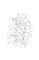
ST−MRAMの模式図を、図6及び図7に示す。図6は斜視図、図7は断面図である。
シリコン基板等の半導体基体60の素子分離層52により分離された部分に、各メモリセルを選択するための選択用トランジスタを構成する、ドレイン領域58、ソース領域57、並びにゲート電極51が、それぞれ形成されている。このうち、ゲート電極51は、図7中前後方向に延びるワード線を兼ねている。
ドレイン領域58は、図7中左右の選択用トランジスタに共通して形成されており、このドレイン領域58には、配線59が接続されている。
そして、ソース領域57と、上方に配置された、図6中左右方向に延びるビット線56との間に、スピントルク磁化反転により磁化の向きが反転する記憶層を有する記憶素子53が配置されている。
A schematic diagram of the ST-MRAM is shown in FIGS. 6 is a perspective view, and FIG. 7 is a cross-sectional view.
A
The
A
この記憶素子53は、例えば磁気トンネル接合素子(MTJ素子)により構成される。記憶素子53は2つの磁性層61、62を有する。この2層の磁性層61,62のうち、一方の磁性層を磁化の向きが固定された磁化固定層として、他方の磁性層を磁化の向きが変化する磁化自由層即ち記憶層とする。
また、記憶素子53は、ビット線56と、ソース領域57とに、それぞれ上下のコンタクト層54を介して接続されている。これにより、記憶素子53に電流を流して、スピン注入により記憶層の磁化の向きを反転させることができる。
The
The
ところでMRAMの場合は、記憶素子とは別に書き込み配線(ワード線やビット線)を設けて、書き込み配線に電流を流して発生する電流磁界により、情報の書き込み(記録)を行っている。そのため、書き込み配線に、書き込みに必要となる電流量を充分に流すことができる。 In the case of the MRAM, a write wiring (word line or bit line) is provided separately from the memory element, and information is written (recorded) by a current magnetic field generated by passing a current through the write wiring. Therefore, a sufficient amount of current required for writing can be passed through the write wiring.
一方、ST−MRAMにおいては、記憶素子に流す電流によりスピントルク磁化反転を行い、記憶層の磁化の向きを反転させる必要がある。
そして、このように記憶素子に直接電流を流して情報の書き込み(記録)を行うことから、書き込みを行うメモリセルを選択するために、記憶素子を選択トランジスタと接続してメモリセルを構成する。この場合、記憶素子に流れる電流は、選択トランジスタに流すことが可能な電流(選択トランジスタの飽和電流)の大きさに制限される。
このため、選択トランジスタの飽和電流以下の電流で書き込みを行う必要があり、トランジスタの飽和電流は微細化に伴って低下することが知られているため、ST−MRAMの微細化のためには、スピントランスファの効率を改善して、記憶素子に流す電流を低減させる必要がある。
On the other hand, in the ST-MRAM, it is necessary to perform spin torque magnetization reversal by a current passed through the storage element to reverse the magnetization direction of the storage layer.
Since the current is directly supplied to the memory element and information is written (recorded) as described above, the memory cell is configured by connecting the memory element to a selection transistor in order to select a memory cell to be written. In this case, the current flowing through the memory element is limited to the magnitude of the current that can flow through the selection transistor (the saturation current of the selection transistor).
For this reason, it is necessary to perform writing at a current equal to or lower than the saturation current of the selection transistor, and it is known that the saturation current of the transistor decreases with miniaturization. It is necessary to improve the efficiency of spin transfer and reduce the current flowing through the memory element.
また、読み出し信号を大きくするためには、大きな磁気抵抗変化率を確保する必要があり、そのためには上述のようなMTJ構造を採用すること、すなわち記憶層の両側に接している中間層をトンネル絶縁層(トンネルバリア層)とした記憶素子の構成にすることが効果的である。
このように中間層としてトンネル絶縁層を用いた場合には、トンネル絶縁層が絶縁破壊することを防ぐために、記憶素子に流す電流量に制限が生じる。すなわち記憶素子の繰り返し書き込みに対する信頼性の確保の観点からも、スピントルク磁化反転に必要な電流を抑制しなくてはならない。
Further, in order to increase the read signal, it is necessary to secure a large magnetoresistance change rate. For this purpose, the MTJ structure as described above is adopted, that is, the intermediate layer in contact with both sides of the storage layer is tunneled. It is effective to adopt a memory element configuration using an insulating layer (tunnel barrier layer).
When the tunnel insulating layer is used as the intermediate layer as described above, the amount of current flowing through the memory element is limited in order to prevent the tunnel insulating layer from being broken down. That is, from the viewpoint of ensuring reliability with respect to repetitive writing of the memory element, the current required for spin torque magnetization reversal must be suppressed.
この電流値を下げるためには、この電流値が記憶層の膜厚に比例し、記憶層の飽和磁化の2乗に比例するので、これら(膜厚や飽和磁化)を調節すれば良いことがわかる(例えば、非特許文献3参照)。
そして、例えば特許文献3には、記録材料の磁化量(Ms)を低減すれば、電流値を低減できることが示されている。
In order to reduce the current value, the current value is proportional to the film thickness of the memory layer and proportional to the square of the saturation magnetization of the memory layer. Therefore, it is only necessary to adjust these (film thickness and saturation magnetization). It is understood (for example, refer nonpatent literature 3).
For example,
しかしながら一方で、ST−MRAMは不揮発メモリであるから、電流によって書き込まれた情報を安定に記憶する必要がある。つまり、記憶層の磁化の熱揺らぎに対する安定性(熱安定性)を確保する必要がある。
また、記憶層の熱安定性が確保されていないと、反転した磁化の向きが、熱(動作環境における温度)により再反転する場合があり、書き込みエラーとなってしまう。
ST−MRAMにおける記憶素子は、従来のMRAMと比較して、スケーリングにおいて有利、すなわち記憶層の体積を小さくすることが可能であるという利点があることを記録電流値の観点で上述した。しかしながら、体積が小さくなることは、他の特性が同一であるならば、熱安定性を低下させる方向にある。
そして、ST−MRAMの大容量化を進めた場合、記録素子の体積は一層小さくなるので、熱安定性の確保は重要な課題となる。
However, on the other hand, since the ST-MRAM is a nonvolatile memory, it is necessary to stably store information written by current. That is, it is necessary to ensure the stability (thermal stability) against the thermal fluctuation of the magnetization of the storage layer.
If the thermal stability of the storage layer is not ensured, the reversed magnetization direction may be reversed again by heat (temperature in the operating environment), resulting in a write error.
It has been described above from the viewpoint of the recording current value that the storage element in the ST-MRAM has an advantage in scaling, that is, it is possible to reduce the volume of the storage layer, compared with the conventional MRAM. However, decreasing the volume tends to decrease thermal stability if other characteristics are the same.
When the capacity of the ST-MRAM is increased, the volume of the recording element is further reduced, so ensuring thermal stability becomes an important issue.
そのため、ST−MRAMにおける記憶素子において、熱安定性は非常に重要な特性であり、体積を減少させてもこの熱安定性が確保されるように設計する必要がある。 Therefore, in the memory element in the ST-MRAM, thermal stability is a very important characteristic, and it is necessary to design the thermal stability to be ensured even if the volume is reduced.
すなわち、ST−MRAMが不揮発メモリとして存在し得るためには、スピントルク磁化反転に必要な電流をトランジスタの飽和電流やトンネルバリアが破壊される電流以下に減らし、また、書き込まれた情報を保持するための熱安定性を確保する必要がある。 That is, in order for the ST-MRAM to exist as a non-volatile memory, the current required for spin torque magnetization reversal is reduced below the saturation current of the transistor and the current that destroys the tunnel barrier, and the written information is retained. Therefore, it is necessary to ensure thermal stability.
以上のように、スピントルク磁化反転に必要な電流を低減するには、記憶層の飽和磁化量Msを低減することや、記憶層を薄くする方法が考えられる。例えば、上述の特許文献3のように、記憶層の材料に、飽和磁化量Msの低い材料を使用することが有効である。
しかしながら、このように、単純に飽和磁化量Msの低い材料を用いた場合、情報を保持するための熱安定性を確保することが困難になる。
そこで本発明においては、書き込み電流を増大させることなく、熱安定性を改善することができる記憶素子、並びにこの記憶素子を有する記憶装置を提供することを目的とする。
As described above, in order to reduce the current required for the spin torque magnetization reversal, it is conceivable to reduce the saturation magnetization amount Ms of the storage layer or to make the storage layer thin. For example, as in
However, as described above, when a material having a low saturation magnetization Ms is simply used, it is difficult to ensure thermal stability for retaining information.
Accordingly, an object of the present invention is to provide a memory element that can improve thermal stability without increasing a write current, and a memory device having the memory element.
本発明の記憶素子は、情報を磁性体の磁化状態により保持する記憶層と、上記記憶層に記憶された情報の基準となる磁化を有する磁化固定層と、上記記憶層と上記磁化固定層の間に設けられる非磁性体による中間層とを有し、上記記憶層、上記中間層、上記磁化固定層を有する層構造の積層方向に流れる電流に伴って発生するスピントルク磁化反転を利用して上記記憶層の磁化を反転させることにより情報の記憶を行う。そして上記記憶層は、鉄(Fe)、コバルト(Co)の少なくとも一方を含有する合金領域を含む。さらに上記記憶層がその磁化反転過程で受ける実効的な反磁界の大きさが、上記記憶層の飽和磁化量よりも小さいものとされている。
また上記記憶層を構成する強磁性材料が、Co−Fe合金からなる。
また上記記憶層が、CoxFe100-x(但しxは原子%で、0≦x≦40)とあらわされ、磁化容易軸方向が膜面に垂直となっている。
或いは、上記記憶層が、(CoxFe100-x)yM1-y(但しMはFe,Co以外の元素、x、yは原子%で、0≦x≦40、0<y<100)とあらわされる合金であり、磁化容易軸方向が膜面に垂直となっている
The storage element of the present invention includes a storage layer that holds information according to the magnetization state of a magnetic material, a magnetization fixed layer that has a magnetization serving as a reference for information stored in the storage layer, and the storage layer and the magnetization fixed layer. A non-magnetic intermediate layer provided between them, and utilizing spin torque magnetization reversal that occurs with a current flowing in the stacking direction of the layer structure including the storage layer, the intermediate layer, and the magnetization fixed layer Information is stored by reversing the magnetization of the storage layer. The memory layer includes an alloy region containing at least one of iron (Fe) and cobalt (Co). Further, the effective demagnetizing field that the storage layer receives in the magnetization reversal process is smaller than the saturation magnetization of the storage layer.
The ferromagnetic material constituting the memory layer is made of a Co—Fe alloy.
The memory layer is expressed as Co x Fe 100-x (where x is atomic%, 0 ≦ x ≦ 40), and the easy axis of magnetization is perpendicular to the film surface.
Alternatively, the storage layer is, (Co x Fe 100-x ) y M 1-y ( wherein M is Fe, elements other than Co, x, y are in atomic%, 0 ≦ x ≦ 40,0 < y <100 ) And the easy axis of magnetization is perpendicular to the film surface.
また、本発明の記憶装置は、情報を磁性体の磁化状態により保持する記憶素子と、互いに交差する2種類の配線とを備え、記憶素子は上記本発明の記憶素子の構成であり、2種類の配線の間に記憶素子が配置され、二種類の配線を通じて、記憶素子に積層方向の電流が流れ、これに伴ってスピントルク磁化反転が起こる。 The memory device of the present invention includes a memory element that holds information according to the magnetization state of the magnetic material, and two kinds of wirings that intersect each other, and the memory element has the configuration of the memory element of the present invention. A storage element is disposed between the two wirings, and a current in the stacking direction flows through the storage element through two types of wirings, and accordingly, spin torque magnetization reversal occurs.
本発明の記憶素子によれば、情報を磁性体の磁化状態により保持する記憶層を有し、この記憶層に対して、中間層を介して磁化固定層が設けられており、積層方向に流れる電流に伴って発生するスピントルク磁化反転を利用して記憶層の磁化を反転させることにより情報の記録が行われるので、積層方向に電流を流すことで情報の記録を行うことができる。このとき、記憶層がその磁化反転過程で受ける実効的な反磁界の大きさは、記憶層の飽和磁化量よりも小さいことにより、記憶層が受ける反磁界が小さくなっており、記憶層の磁化の向きを反転させるために必要となる書き込み電流値を低減することができる。
一方で、記憶層の飽和磁化量を低減しなくても書き込み電流量を低減させることができるため、記憶層の熱安定性は十分に保つために必要な飽和磁化量を確保することができる。
According to the memory element of the present invention, it has a memory layer that holds information according to the magnetization state of the magnetic substance, and the magnetization pinned layer is provided to the memory layer via the intermediate layer, and flows in the stacking direction. Since information recording is performed by reversing the magnetization of the storage layer using spin torque magnetization reversal that occurs with current, information can be recorded by flowing current in the stacking direction. At this time, the effective demagnetizing field that the storage layer receives in the magnetization reversal process is smaller than the saturation magnetization of the storage layer, so that the demagnetizing field received by the storage layer is small, and the magnetization of the storage layer The write current value required for reversing the direction can be reduced.
On the other hand, since the amount of write current can be reduced without reducing the amount of saturation magnetization of the storage layer, the amount of saturation magnetization necessary for sufficiently maintaining the thermal stability of the storage layer can be ensured.
また、本発明の記憶装置の構成によれば、2種類の配線を通じて、記憶素子に積層方向の電流が流れ、スピントランスファが起こることにより、2種類の配線を通じて記憶素子の積層方向に電流を流してスピントルク磁化反転による情報の記録を行うことができる。
また、記憶層の飽和磁化量を低減しなくても書き込み電流量を低減させることが可能になるため、記憶素子に記録された情報を安定に保持し、かつ記憶装置の微細化、信頼性の向上、低消費電力化を実現することが可能になる。
In addition, according to the configuration of the memory device of the present invention, a current in the stacking direction flows through the memory element through two types of wiring, and a current flows in the stacking direction of the memory element through the two types of wiring due to spin transfer. Thus, information can be recorded by spin torque magnetization reversal.
In addition, since it becomes possible to reduce the amount of write current without reducing the saturation magnetization amount of the storage layer, the information recorded in the storage element can be stably held, and the memory device can be miniaturized and reliable. Improvement and reduction in power consumption can be realized.
本発明によれば、記憶層の飽和磁化量を低減しなくても、記憶素子の書き込み電流量を低減することが可能になるため、情報保持能力である熱安定性を充分に確保して、特性バランスに優れた記憶素子を構成することができる。
これにより、動作エラーをなくして、記憶素子の動作マージンを充分に得ることができる。
従って、安定して動作する、信頼性の高いメモリを実現することができる。
また、書き込み電流を低減して、記憶素子に書き込みを行う際の消費電力を低減することが可能になる。
従って、記憶装置全体の消費電力を低減することが可能になる。
According to the present invention, it is possible to reduce the write current amount of the storage element without reducing the saturation magnetization amount of the storage layer. A memory element having excellent characteristic balance can be configured.
Thereby, an operation error can be eliminated and a sufficient operation margin of the memory element can be obtained.
Therefore, a highly reliable memory that operates stably can be realized.
In addition, the write current can be reduced, so that power consumption when writing to the memory element can be reduced.
Therefore, the power consumption of the entire storage device can be reduced.
以下、本発明の実施の形態を次の順序で説明する。
<1.実施の形態の記憶素子の概要>
<2.実施の形態の構成>
<3.実験>
Hereinafter, embodiments of the present invention will be described in the following order.
<1. Outline of Memory Element of Embodiment>
<2. Configuration of Embodiment>
<3. Experiment>
<1.実施の形態の記憶素子の概要>
まず、発明の実施の形態となる記憶素子の概要について説明する。
本発明の実施の形態は、前述したスピントルク磁化反転により、記憶素子の記憶層の磁化の向きを反転させて、情報の記録を行うものである。
記憶層は、強磁性層等の磁性体により構成され、情報を磁性体の磁化状態(磁化の向き)により保持するものである。
<1. Outline of Memory Element of Embodiment>
First, an outline of a memory element according to an embodiment of the invention will be described.
In the embodiment of the present invention, information is recorded by reversing the magnetization direction of the memory layer of the memory element by the spin torque magnetization reversal described above.
The memory layer is made of a magnetic material such as a ferromagnetic layer, and holds information by the magnetization state (magnetization direction) of the magnetic material.
記憶素子は、例えば図2に一例を示す層構造とされ、少なくとも2つの強磁性体層としての記憶層17、磁化固定層15を備え、またその2つの磁性層の間の中間層16を備える。
記憶層17は、膜面に垂直な磁化を有し、情報に対応して磁化の向きが変化される。
磁化固定層15は、記憶層15に記憶された情報の基準となる膜面に垂直な磁化を有する。
中間層16は、非磁性体であって、記憶層17と磁化固定層15の間に設けられる。
そして記憶層17、中間層16、磁化固定層15を有する層構造の積層方向にスピン偏極した電子を注入することにより、記憶層17の磁化の向きが変化して、記憶層17に対して情報の記録が行われる。
The storage element has a layer structure as shown in FIG. 2, for example, and includes at least two storage layers 17 as ferromagnetic layers and a fixed
The storage layer 17 has magnetization perpendicular to the film surface, and the magnetization direction is changed in accordance with information.
The magnetization fixed
The
Then, by injecting spin-polarized electrons in the stacking direction of the layer structure including the storage layer 17, the
ここでスピントルク磁化反転について簡単に説明する。
電子は2種類のスピン角運動量をもつ。仮にこれを上向き、下向きと定義する。非磁性体内部では両者が同数であり、強磁性体内部では両者の数に差がある。ST−MRAMを構成する2層の強磁性体である磁化固定層15及び記憶層17において、互いの磁気モーメントの向きが反方向状態のときに、電子を磁化固定層15から記憶層17への移動させた場合について考える。
Here, the spin torque magnetization reversal will be briefly described.
Electrons have two types of spin angular momentum. This is defined as upward and downward. The number of both is the same inside the non-magnetic material, and the number of both is different inside the ferromagnetic material. In the magnetization fixed
磁化固定層15は、高い保磁力のために磁気モーメントの向きが固定された固定磁性層である。
磁化固定層15を通過した電子はスピン偏極、すなわち上向きと下向きの数に差が生じる。非磁性層である中間層16の厚さが充分に薄く構成されていると、磁化固定層15の通過によるスピン偏極が緩和して通常の非磁性体における非偏極(上向きと下向きが同数)状態になる前に他方の磁性体、すなわち記憶層17に電子が達する。
記憶層17では、スピン偏極度の符号が逆になっていることにより、系のエネルギを下げるために一部の電子は反転、すなわちスピン角運動量の向きをかえさせられる。このとき、系の全角運動量は保存されなくてはならないため、向きを変えた電子による角運動量変化の合計と等価な反作用が記憶層17の磁気モーメントにも与えられる。
The magnetization fixed
The electrons that have passed through the magnetization pinned
In the memory layer 17, since the signs of the spin polarization are reversed, some electrons are inverted, that is, the direction of the spin angular momentum is changed in order to lower the energy of the system. At this time, since the total angular momentum of the system must be preserved, a reaction equivalent to the sum of changes in angular momentum due to the electrons whose direction is changed is also given to the magnetic moment of the storage layer 17.
電流すなわち単位時間に通過する電子の数が少ない場合には、向きを変える電子の総数も少ないために記憶層17の磁気モーメントに発生する角運動量変化も小さいが、電流が増えると多くの角運動量変化を単位時間内に与えることができる。
角運動量の時間変化はトルクであり、トルクがあるしきい値を超えると記憶層17の磁気モーメントは歳差運動を開始し、その一軸異方性により180度回転したところで安定となる。すなわち反方向状態から同方向状態への反転が起こる。
When the current, that is, the number of electrons passing through the unit time is small, the total number of electrons changing the direction is small, and therefore the change in the angular momentum generated in the magnetic moment of the storage layer 17 is small. Changes can be given within a unit time.
The time change of the angular momentum is torque, and when the torque exceeds a certain threshold value, the magnetic moment of the storage layer 17 starts precession and becomes stable when rotated 180 degrees due to its uniaxial anisotropy. That is, inversion from the opposite direction state to the same direction state occurs.
磁化が同方向状態にあるとき、電流を逆に記憶層17から磁化固定層15へ電子を送る向きに流すと、今度は磁化固定層15で反射される際にスピン反転した電子が記憶層17に進入する際にトルクを与え、反方向状態へと磁気モーメントを反転させることができる。ただしこの際、反転を起こすのに必要な電流量は、反方向状態から同方向状態へと反転させる場合よりも多くなる。
When the magnetization is in the same direction state, if a current is flowed in the opposite direction to send electrons from the storage layer 17 to the magnetization fixed
磁気モーメントの同方向状態から反方向状態への反転は直感的な理解が困難であるが、磁化固定層15が固定されているために磁気モーメントが反転できず、系全体の角運動量を保存するために記憶層17が反転する、と考えてもよい。このように、0/1の記録は、磁化固定層15から記憶層17の方向またはその逆向きに、それぞれの極性に対応する、あるしきい値以上の電流を流すことによって行われる。
Although it is difficult to intuitively understand the reversal of the magnetic moment from the same direction to the opposite direction, the magnetic moment cannot be reversed because the magnetization fixed
情報の読み出しは、従来型のMRAMと同様、磁気抵抗効果を用いて行われる。すなわち上述の記録の場合と同様に膜面垂直方向に電流を流す。そして、記憶層17の磁気モーメントが、磁化固定層15の磁気モーメントに対して同方向であるか反方向であるかに従い、素子の示す電気抵抗が変化する現象を利用する。
Information is read out by using the magnetoresistive effect as in the conventional MRAM. That is, a current is passed in the direction perpendicular to the film surface as in the case of the above recording. Then, a phenomenon is used in which the electric resistance of the element changes depending on whether the magnetic moment of the storage layer 17 is in the same direction or in the opposite direction to the magnetic moment of the magnetization fixed
磁化固定層15と記憶層17の間の中間層16として用いる材料は金属でも絶縁体でも構わないが、より高い読み出し信号(抵抗の変化率)が得られ、かつより低い電流によって記録が可能とされるのは、中間層として絶縁体を用いた場合である。このときの素子を強磁性トンネル接合(Magnetic Tunnel Junction:MTJ)と呼ぶ。
The material used for the
スピントルク磁化反転によって、磁性層の磁化の向きを反転させるときに、必要となる電流の閾値Icは、下記式(1)により表される。 When the magnetization direction of the magnetic layer is reversed by spin torque magnetization reversal, the required current threshold Ic is expressed by the following equation (1).

式(1)で表されるように、電流の閾値は、磁性層の体積V、磁性層の飽和磁化Ms、スピン注入効率η、スピン制動定数αを制御することにより、任意に設定することが可能である。 As represented by Equation (1), the current threshold can be arbitrarily set by controlling the volume V of the magnetic layer, the saturation magnetization Ms of the magnetic layer, the spin injection efficiency η, and the spin braking constant α. Is possible.
本実施の形態では、磁化状態により情報を保持することができる磁性層(記憶層17)と、磁化の向きが固定された磁化固定層15とを有する記憶素子を構成する。
メモリとして存在し得るためには、書き込まれた情報を保持することができなければならない。情報を保持する能力の指標として、熱安定性の指標Δ(=KV/kBT)の値で判断される。このΔは、下記式(2)により表される。
In the present embodiment, a storage element including a magnetic layer (storage layer 17) capable of holding information depending on the magnetization state and a magnetization fixed
In order to be able to exist as a memory, it must be able to hold the written information. As an index of the ability to hold information, it is determined by the value of the thermal stability index Δ (= KV / k B T). This Δ is represented by the following formula (2).
実効的な異方性磁界Hkには、形状磁気異方性、誘導磁気異方性、結晶磁気異方性等の影響が取り込まれており、単磁区の一斉回転モデルを仮定した場合、これは保磁力と同等となる。 The effect of shape magnetic anisotropy, induced magnetic anisotropy, crystal magnetic anisotropy, etc. is incorporated into the effective anisotropy magnetic field Hk. Equivalent to coercive force.
熱安定性の指標Δと電流の閾値Icとは、トレードオフの関係になることが多い。そのため、メモリ特性を維持するには、これらの両立が課題となることが多い。 The thermal stability index Δ and the current threshold value Ic often have a trade-off relationship. Therefore, in order to maintain the memory characteristics, it is often a problem to achieve both.
記憶層の磁化状態を変化させる電流の閾値は、実際には、例えば記憶層17の厚さが2nmであり、平面パターンが100nm×150nmの略楕円形のTMR素子において、+側の閾値+Ic=+0.5mAであり、−側の閾値−Ic=−0.3mAであり、その際の電流密度は約3.5×10⁶A/cm2である。これらは、上記の式(1)にほぼ一致する。 The threshold value of the current for changing the magnetization state of the storage layer is actually a threshold value on the + side + Ic = in a substantially elliptic TMR element having a thickness of the storage layer 17 of, for example, 2 nm and a planar pattern of 100 nm × 150 nm. +0.5 mA, −side threshold −Ic = −0.3 mA, and the current density at that time is about 3.5 × 10 6 A / cm 2 . These are almost in agreement with the above formula (1).
これに対して、電流磁場により磁化反転を行う通常のMRAMでは、書き込み電流が数mA以上必要となる。
従って、ST−MRAMの場合には、上述のように書き込み電流の閾値が充分に小さくなるため、集積回路の消費電力を低減させるために有効であることが分かる。
また、通常のMRAMで必要とされる、電流磁界発生用の配線が不要となるため、集積度においても通常のMRAMに比較して有利である。
On the other hand, in a normal MRAM that performs magnetization reversal by a current magnetic field, a write current of several mA or more is required.
Therefore, in the case of the ST-MRAM, it can be understood that the write current threshold is sufficiently small as described above, which is effective in reducing the power consumption of the integrated circuit.
In addition, since a wiring for generating a current magnetic field, which is required in a normal MRAM, is not necessary, the degree of integration is advantageous as compared with a normal MRAM.
そして、スピントルク磁化反転を行う場合には、記憶素子に直接電流を流して情報の書き込み(記録)を行うことから、書き込みを行うメモリセルを選択するために、記憶素子を選択トランジスタと接続してメモリセルを構成する。
この場合、記憶素子に流れる電流は、選択トランジスタで流すことが可能な電流(選択トランジスタの飽和電流)の大きさによって制限される。
When spin torque magnetization reversal is performed, current is directly supplied to the storage element to write (record) information. Therefore, in order to select a memory cell to be written, the storage element is connected to a selection transistor. To constitute a memory cell.
In this case, the current flowing through the memory element is limited by the magnitude of the current that can be passed through the selection transistor (the saturation current of the selection transistor).
選択トランジスタの飽和電流よりも、スピン注入による磁化反転の電流の閾値Icを小さくするためには、式(1)より、記憶層17の飽和磁化量Msを減らせば良いことがわかる。
しかし、単純に飽和磁化量Msを減らした場合(例えば、特許文献3)には、記憶層17の熱安定性が著しく損なわれ、メモリとしての機能を果せなくなる。
メモリを構成するためには、熱安定性の指標Δがある程度以上の大きさである必要がある。
It can be seen from equation (1) that the saturation magnetization amount Ms of the memory layer 17 can be reduced in order to make the threshold value Ic of the magnetization reversal current by spin injection smaller than the saturation current of the selection transistor.
However, when the saturation magnetization amount Ms is simply reduced (for example, Patent Document 3), the thermal stability of the storage layer 17 is significantly impaired, and the function as a memory cannot be performed.
In order to configure the memory, it is necessary that the thermal stability index Δ is larger than a certain level.
そこで、本願の発明者等が種々の検討を行った結果、記憶層17を構成する強磁性層をコバルト(Co)および鉄(Fe)からなる合金とし、このCo−Feの組成を選定することにより、記憶層17が受ける実効的な反磁界(Meffective)の大きさが、記憶層17の飽和磁化量Msよりも小さくなることを見出した。
上述の強磁性材料を用いることにより、記憶層17が受ける実効的な反磁界の大きさが、記憶層の飽和磁化量Msよりも小さい構成となる。
これにより、記憶層17が受ける反磁界を小さくすることができるので、式(2)により表される熱安定性Δを損ねることなく、式(1)中により表される電流の閾値Icを低減する効果が得られる。
さらに、発明者らは、上記の選定されたCo−Fe組成の内、限られた組成範囲において、Co−Feが膜面垂直方向に磁化し、それにより、Gbitクラスの容量を実現可能な極微小記録素子においても十分な熱安定性が確保可能であることを見出した。
従って、GbitクラスのST−MRAMにおいて熱安定性を保った状態で、低電流で情報の書き込みができる、という安定したメモリの形成を可能にする。
Therefore, as a result of various studies by the inventors of the present application, the ferromagnetic layer constituting the memory layer 17 is made of an alloy composed of cobalt (Co) and iron (Fe), and the composition of this Co—Fe is selected. Thus, it has been found that the effective demagnetizing field (Meffective) received by the storage layer 17 is smaller than the saturation magnetization Ms of the storage layer 17.
By using the above-described ferromagnetic material, the effective demagnetizing field received by the storage layer 17 is smaller than the saturation magnetization Ms of the storage layer.
As a result, the demagnetizing field received by the storage layer 17 can be reduced, and the current threshold value Ic represented by the equation (1) is reduced without impairing the thermal stability Δ represented by the equation (2). Effect is obtained.
Furthermore, the inventors have confirmed that Co—Fe is magnetized in the direction perpendicular to the film surface in the limited composition range of the above selected Co—Fe composition, thereby achieving a Gbit class capacity. It has been found that sufficient thermal stability can be secured even in a small recording element.
Accordingly, it is possible to form a stable memory in which information can be written with a low current while maintaining thermal stability in the Gbit class ST-MRAM.
本実施の形態では、記憶層17が受ける実効的な反磁界の大きさが、記憶層17の飽和磁化量Msよりも小さい構成、即ち、記憶層17の飽和磁化量Msに対する実効的な反磁界の大きさの比の値を1より小さくする。 In the present embodiment, the effective demagnetizing field received by the storage layer 17 is smaller than the saturation magnetization amount Ms of the storage layer 17, that is, the effective demagnetizing field with respect to the saturation magnetization amount Ms of the storage layer 17. The value of the size ratio is made smaller than 1.
さらに、選択トランジスタの飽和電流値を考慮して、記憶層17と磁化固定層15との間の非磁性の中間層16として、絶縁体から成るトンネル絶縁層を用いて磁気トンネル接合(MTJ)素子を構成する。
トンネル絶縁層を用いて磁気トンネル接合(MTJ)素子を構成することにより、非磁性導電層を用いて巨大磁気抵抗効果(GMR)素子を構成した場合と比較して、磁気抵抗変化率(MR比)を大きくすることができ、読み出し信号強度を大きくすることができるためである。
Further, in consideration of the saturation current value of the selection transistor, a magnetic tunnel junction (MTJ) element using a tunnel insulating layer made of an insulator as the nonmagnetic
By constructing a magnetic tunnel junction (MTJ) element using a tunnel insulating layer, a magnetoresistance change rate (MR ratio) is compared with a case where a giant magnetoresistive effect (GMR) element is constructed using a nonmagnetic conductive layer. This is because the read signal intensity can be increased.
そして、特に、このトンネル絶縁層としての中間層16の材料として、酸化マグネシウム(MgO)を用いることにより、これまで一般的に用いられてきた酸化アルミニウムを用いた場合よりも、磁気抵抗変化率(MR比)を大きくすることができる。
また、一般に、スピントランスファの効率はMR比に依存し、MR比が大きいほど、スピントランスファの効率が向上し、磁化反転電流密度を低減することができる。
従って、トンネル絶縁層の材料として酸化マグネシウムを用い、同時に上記の記憶層17を用いることにより、スピントルク磁化反転による書き込み閾値電流を低減することができ、少ない電流で情報の書き込み(記録)を行うことができる。また、読み出し信号強度を大きくすることができる。
これにより、MR比(TMR比)を確保して、スピントルク磁化反転による書き込み閾値電流を低減することができ、少ない電流で情報の書き込み(記録)を行うことができる。また、読み出し信号強度を大きくすることができる。
In particular, by using magnesium oxide (MgO) as the material of the
In general, the efficiency of the spin transfer depends on the MR ratio, and as the MR ratio increases, the efficiency of the spin transfer improves and the magnetization reversal current density can be reduced.
Therefore, by using magnesium oxide as the material of the tunnel insulating layer and simultaneously using the memory layer 17 described above, the write threshold current due to the spin torque magnetization reversal can be reduced, and information is written (recorded) with a small current. be able to. In addition, the read signal intensity can be increased.
Thereby, the MR ratio (TMR ratio) can be secured, the write threshold current due to the spin torque magnetization reversal can be reduced, and information can be written (recorded) with a small current. In addition, the read signal intensity can be increased.
このようにトンネル絶縁層を酸化マグネシウム(MgO)膜により形成する場合には、MgO膜が結晶化していて、001方向に結晶配向性を維持していることがより望ましい。 Thus, when the tunnel insulating layer is formed of a magnesium oxide (MgO) film, it is more desirable that the MgO film is crystallized and the crystal orientation is maintained in the 001 direction.
なお、本実施の形態において、記憶層17と磁化固定層15との間の中間層16(トンネル絶縁層)は、酸化マグネシウムから成る構成とする他にも、例えば酸化アルミニウム、窒化アルミニウム、SiO2、Bi2O3、MgF2、CaF、SrTiO2、AlLaO3、Al−N−O等の各種の絶縁体、誘電体、半導体を用いて構成することもできる。
In the present embodiment, the intermediate layer 16 (tunnel insulating layer) between the storage layer 17 and the magnetization fixed
トンネル絶縁層の面積抵抗値は、スピントルク磁化反転により記憶層17の磁化の向きを反転させるために必要な電流密度を得る観点から、数十Ωμm2程度以下に制御する必要がある。
そして、MgO膜から成るトンネル絶縁層では、面積抵抗値を上述の範囲とするために、MgO膜の膜厚を1.5nm以下に設定する必要がある。
The area resistance value of the tunnel insulating layer needs to be controlled to about several tens of Ωμm 2 or less from the viewpoint of obtaining a current density necessary for reversing the magnetization direction of the memory layer 17 by spin torque magnetization reversal.
In the tunnel insulating layer made of the MgO film, the film thickness of the MgO film needs to be set to 1.5 nm or less in order to make the sheet resistance value in the above range.
また、記憶層17の磁化の向きを、小さい電流で容易に反転できるように、記憶素子を小さくすることが望ましい。
従って、好ましくは、記憶素子の面積を0.01μm2以下とする。
In addition, it is desirable to make the memory element small so that the magnetization direction of the memory layer 17 can be easily reversed with a small current.
Therefore, preferably, the area of the memory element is 0.01 μm 2 or less.
また、本発明の実施の形態としての記憶層17には、Co、Fe以外の元素を添加することも可能である。
異種元素の添加により、拡散の防止による耐熱性の向上や磁気抵抗効果の増大、平坦化に伴う絶縁耐圧の増大などの効果が得られる。この場合の添加元素の材料としては、B、C、N、O、F、Mg、Si、P、Ti、V、Cr、Mn、Ni、Cu、Ge、Nb、Mo、Ru、Rh、Pd、Ag、Ta、W、Ir、Pt、Au、Zr、Hf、Re、Osまたはそれらの合金を用いることができる。
It is also possible to add elements other than Co and Fe to the memory layer 17 as an embodiment of the present invention.
By adding different elements, effects such as an improvement in heat resistance by preventing diffusion, an increase in magnetoresistance effect, and an increase in withstand voltage due to planarization can be obtained. As the material of the additive element in this case, B, C, N, O, F, Mg, Si, P, Ti, V, Cr, Mn, Ni, Cu, Ge, Nb, Mo, Ru, Rh, Pd, Ag, Ta, W, Ir, Pt, Au, Zr, Hf, Re, Os, or alloys thereof can be used.
なお、本発明における記憶層17は組成の異なる他の強磁性層を直接積層させることも可能である。また、強磁性層と軟磁性層とを積層させたり、複数層の強磁性層を軟磁性層や非磁性層を介して積層させたりすることも可能である。このように積層させた場合でも、本発明でいう効果が得られる。
特に複数層の強磁性層を非磁性層に介して積層させた構成としたときには、強磁性層の層間の相互作用の強さを調整することが可能になるため、記憶素子の寸法がサブミクロン以下になっても、磁化反転電流が大きくならないように抑制することが可能になるという効果が得られる。この場合の非磁性層の材料としては、Ru,Os,Re,Ir,Au,Ag,Cu,Al,Bi,Si,B,C,Cr,Ta,Pd,Pt,Zr,Hf,W,Mo,Nbまたはそれらの合金を用いることができる。
The memory layer 17 in the present invention can be directly laminated with other ferromagnetic layers having different compositions. It is also possible to stack a ferromagnetic layer and a soft magnetic layer, or to stack a plurality of ferromagnetic layers via a soft magnetic layer or a nonmagnetic layer. Even when laminated in this way, the effect referred to in the present invention can be obtained.
In particular, when a configuration in which a plurality of ferromagnetic layers are laminated via a nonmagnetic layer, the strength of the interaction between the ferromagnetic layers can be adjusted. Even if it becomes below, the effect that it becomes possible to suppress so that a magnetization reversal current may not become large is acquired. The material of the nonmagnetic layer in this case is Ru, Os, Re, Ir, Au, Ag, Cu, Al, Bi, Si, B, C, Cr, Ta, Pd, Pt, Zr, Hf, W, Mo. , Nb or their alloys can be used.
磁化固定層15及び記憶層17は、一方向の異方性を有していることが望ましい。
また、磁化固定層15及び記憶層17のそれぞれの膜厚は、0.5nm〜30nmであることが好ましい。
It is desirable that the magnetization fixed
The film thicknesses of the magnetization fixed
記憶素子のその他の構成は、スピントルク磁化反転により情報を記録する記憶素子の従来公知の構成と同様とすることができる。 The other configuration of the storage element can be the same as the conventionally known configuration of the storage element that records information by spin torque magnetization reversal.
磁化固定層15は、強磁性層のみにより、或いは反強磁性層と強磁性層の反強磁性結合を利用することにより、その磁化の向きが固定された構成とすることが出来る。
また、磁化固定層15は、単層の強磁性層から成る構成、或いは複数層の強磁性層を非磁性層を介して積層した積層フェリピン構造とすることが出来る。
積層フェリピン構造の磁化固定層15を構成する強磁性層の材料としては、Co,CoFe,CoFeB等を用いることができる。また、非磁性層の材料としては、Ru,Re,Ir,Os等を用いることができる。
The magnetization pinned
In addition, the magnetization fixed
Co, CoFe, CoFeB, or the like can be used as the material of the ferromagnetic layer constituting the magnetization fixed
反強磁性層の材料としては、FeMn合金、PtMn合金、PtCrMn合金、NiMn合金、IrMn合金、NiO、Fe2O3等の磁性体を挙げることができる。
また、これらの磁性体に、Ag,Cu,Au,Al,Si,Bi,Ta,B,C,O,N,Pd,Pt,Zr,Hf,Ir,W,Mo,Nb等の非磁性元素を添加して、磁気特性を調整したり、その他の結晶構造や結晶性や物質の安定性等の各種物性を調整したりすることができる。
Examples of the material of the antiferromagnetic layer include magnetic materials such as FeMn alloy, PtMn alloy, PtCrMn alloy, NiMn alloy, IrMn alloy, NiO, and Fe 2 O 3 .
In addition, nonmagnetic elements such as Ag, Cu, Au, Al, Si, Bi, Ta, B, C, O, N, Pd, Pt, Zr, Hf, Ir, W, Mo, and Nb are included in these magnetic materials. Can be added to adjust the magnetic properties and other physical properties such as crystal structure, crystallinity and material stability.
また、記憶素子の膜構成は、記憶層17が磁化固定層15の下側に配置される構成でも、下側に配置される構成でも全く問題はない。さらには、磁化固定層15が記録層17の上下に存在する、いわゆるデュアル構造でも全く問題ない。
In addition, the film configuration of the storage element has no problem whether the storage layer 17 is disposed below the magnetization fixed
なお、記憶素子の記憶層17に記録された情報を読み出す方法としては、記憶素子の記憶層17に薄い絶縁膜を介して、情報の基準となる磁性層を設けて、絶縁層(中間層16)を介して流れる強磁性トンネル電流によって読み出してもよいし、磁気抵抗効果により読み出してもよい。
As a method of reading information recorded in the memory layer 17 of the memory element, a magnetic layer serving as a reference for information is provided on the memory layer 17 of the memory element via a thin insulating film, and an insulating layer (intermediate layer 16) is provided. ) May be read out by a ferromagnetic tunnel current flowing through, or may be read out by a magnetoresistive effect.
<2.実施の形態の構成>
続いて、本発明の実施の形態の具体的構成について説明する。
本発明の一実施の形態として、メモリ装置の概略構成図(斜視図)を図1に示す。
このメモリ装置は、互いに直交する2種類のアドレス配線(例えばワード線とビット線)の交点付近に、磁化状態で情報を保持することができる記憶素子3が配置されて成る。
即ち、シリコン基板等の半導体基体10の素子分離層2により分離された部分に、各メモリセルを選択するための選択用トランジスタを構成する、ドレイン領域8、ソース領域7、並びにゲート電極1が、それぞれ形成されている。このうち、ゲート電極1は、図中前後方向に延びる一方のアドレス配線(例えばワード線)を兼ねている。
ドレイン領域8は、図中左右の選択用トランジスタに共通して形成されており、このドレイン領域8には、配線9が接続されている。
<2. Configuration of Embodiment>
Next, a specific configuration of the embodiment of the present invention will be described.
As an embodiment of the present invention, a schematic configuration diagram (perspective view) of a memory device is shown in FIG.
In this memory device, a
That is, the
The
そして、ソース領域7と、上方に配置された、図中左右方向に延びる他方のアドレス配線(例えばビット線)6との間に、記憶素子3が配置されている。この記憶素子3は、スピン注入により磁化の向きが反転する強磁性層から成る記憶層を有する。
また、この記憶素子3は、2種類のアドレス配線1,6の交点付近に配置されている。
この記憶素子3は、ビット線6と、ソース領域7とに、それぞれ上下のコンタクト層4を介して接続されている。
これにより、2種類のアドレス配線1,6を通じて、記憶素子3に上下方向の電流を流して、スピントルク磁化反転により記憶層の磁化の向きを反転させることができる。
The
The
The
As a result, a current in the vertical direction can be passed through the
また、本実施の形態のメモリの記憶素子3の断面図を図2に示す。
図2に示すように、この記憶素子3は、スピントルク磁化反転により磁化M17の向きが反転する記憶層17に対して、下層に磁化固定層15を設けている。
ST−MRAMにおいては、記録層17の磁化M17と磁化固定層15の磁化M15の相対的な角度によって情報の0、1を規定している。
記憶層17と磁化固定層15との間には、トンネルバリア層(トンネル絶縁層)となる中間層16が設けられ、記憶層17と磁化固定層15とにより、MTJ素子が構成されている。
また、磁化固定層15の下には下地層14が形成され、記憶層17の上にはキャップ層18が形成されている。
A cross-sectional view of the
As shown in FIG. 2, the
In the ST-MRAM, 0 or 1 of information is defined by the relative angle between the magnetization M17 of the recording layer 17 and the magnetization M15 of the magnetization fixed
An
A
本実施の形態においては、特に、記憶層17が受ける実効的な反磁界の大きさが記憶層17の飽和磁化量Msよりも小さくなるように、記憶素子3の記憶層17の組成が調整されていることを特徴とする。
即ち、前述したように、記憶層17の強磁性材料Co−Fe組成を選定し、記憶層17が受ける実効的な反磁界の大きさを低くして、記憶層17の飽和磁化量Msよりも小さくなるようにする。
In the present embodiment, in particular, the composition of the storage layer 17 of the
That is, as described above, the composition of the ferromagnetic material Co—Fe of the storage layer 17 is selected, the magnitude of the effective demagnetizing field received by the storage layer 17 is reduced, and the saturation magnetization Ms of the storage layer 17 is exceeded. Make it smaller.
さらに、本実施の形態において、中間層16を、酸化マグネシウム層とした場合には、磁気抵抗変化率(MR比)を高くすることができる。
このようにMR比を高くすることによって、スピン注入の効率を向上して、記憶層17の磁化M1の向きを反転させるために必要な電流密度を低減することができる。
Furthermore, in the present embodiment, when the
By increasing the MR ratio in this way, the efficiency of spin injection can be improved, and the current density required for reversing the direction of the magnetization M1 of the storage layer 17 can be reduced.
本実施の形態の記憶素子3は、下地層14からキャップ層18までを真空装置内で連続的に形成して、その後エッチング等の加工により記憶素子3のパターンを形成することにより、製造することができる。
The
上述の本実施の形態によれば、記憶素子3の記憶層17が、記憶層17が受ける実効的な反磁界の大きさが記憶層17の飽和磁化量Msよりも小さくなるように構成されているので、記憶層17が受ける反磁界が低くなっており、記憶層17の磁化M17の向きを反転させるために必要となる、書き込み電流量を低減することができる。
一方、記憶層17の飽和磁化量Msを低減しなくても書き込み電流量を低減することができるため、記憶層17の飽和磁化量Msを充分な量として、記憶層17の熱安定性を充分に確保することが可能になる。
According to the above-described embodiment, the storage layer 17 of the
On the other hand, since the amount of write current can be reduced without reducing the saturation magnetization amount Ms of the storage layer 17, the thermal stability of the storage layer 17 is sufficient with the saturation magnetization amount Ms of the storage layer 17 sufficient. Can be secured.
このように、情報保持能力である熱安定性を充分に確保することができるため、特性バランスに優れた記憶素子3を構成することができる。
これにより、動作エラーをなくして、記憶素子3の動作マージンを充分に得ることができ、記憶素子3を安定して動作させることができる。
従って、安定して動作する、信頼性の高いメモリを実現することができる。
As described above, since the thermal stability as the information holding capability can be sufficiently ensured, the
As a result, an operation error can be eliminated, a sufficient operation margin of the
Therefore, a highly reliable memory that operates stably can be realized.
また、書き込み電流を低減して、記憶素子3に書き込みを行う際の消費電力を低減することが可能になる。
従って、本実施の形態の記憶素子3によりメモリセルを構成した、メモリ全体の消費電力を低減することが可能になる。
In addition, it is possible to reduce the write current and reduce the power consumption when writing to the
Therefore, it is possible to reduce the power consumption of the entire memory in which the memory cell is configured by the
従って、情報保持特性が優れた、安定して動作する信頼性の高いメモリを実現することができ、記憶素子3を備えたメモリにおいて、消費電力を低減することができる。
Accordingly, a highly reliable memory that has excellent information retention characteristics and operates stably can be realized, and power consumption can be reduced in the memory including the
また、図2に示した記憶素子3を備え、図1に示した構成のメモリは、メモリを製造する際に、一般の半導体MOS形成プロセスを適用できるという利点を有している。
従って、本実施の形態のメモリを、汎用メモリとして適用することが可能になる。
Further, the memory having the
Therefore, the memory of this embodiment can be applied as a general-purpose memory.
<3.実験>
ここで、本実施の形態の記憶素子3の構成において、具体的に記憶層17を構成する強磁性層の材料を選定することにより、記憶層17が受ける実効的な反磁界の大きさを調整して、記憶素子3の試料を作製し、その特性を調べた。
<3. Experiment>
Here, in the configuration of the
実際のメモリ装置には、図1に示したように、記憶素子3以外にもスイッチング用の半導体回路等が存在するが、ここでは、記憶層17の磁化反転特性を調べる目的で、記憶素子のみを形成したウェハにより検討を行った。
As shown in FIG. 1, an actual memory device includes a semiconductor circuit for switching in addition to the
[実験1]
厚さ0.725mmのシリコン基板上に、厚さ300nmの熱酸化膜を形成し、その上に図2に示した構成の記憶素子3を形成した。
具体的には、図2に示した構成の記憶素子3において、各層の材料及び膜厚を次のように選定した。
・下地層14:膜厚10nmのTa膜と膜厚25nmのRu膜の積層膜
・磁化固定層15:膜厚2.5nmのCoFeB膜
・中間層(トンネル絶縁層)16:膜厚0.9nmの酸化マグネシウム膜
・記憶層17:CoFe膜
・キャップ層18:膜厚3nmのTa膜、膜厚3nmのRu膜、膜厚3nmのTa膜の積層膜
このように各層を選定し、また下地層14とシリコン基板との間に図示しない膜厚100nmのCu膜(後述するワード線となるもの)を設けた。
上記膜構成で、記憶層17の強磁性層は、材質をCo−Feの2元系合金とし、強磁性層の膜厚を2.0nmに固定した。
[Experiment 1]
A thermal oxide film having a thickness of 300 nm was formed on a silicon substrate having a thickness of 0.725 mm, and the
Specifically, in the
-Underlayer 14: Laminated film of Ta film with a film thickness of 10 nm and Ru film with a film thickness of 25 nm-Magnetization fixed layer 15: CoFeB film with a film thickness of 2.5 nm-Intermediate layer (tunnel insulating layer) 16: Film thickness of 0.9 nm Magnesium oxide film / memory layer 17: CoFe film / cap layer 18: laminated film of 3 nm thick Ta film, 3 nm thick Ru film, 3 nm thick Ta film A Cu film (not shown) having a film thickness of 100 nm (to be described later) was provided between 14 and the silicon substrate.
In the above-described film configuration, the ferromagnetic layer of the memory layer 17 is made of a Co—Fe binary alloy, and the thickness of the ferromagnetic layer is fixed at 2.0 nm.
酸化マグネシウム膜から成る中間層16以外の各層は、DCマグネトロンスパッタ法を用いて成膜した。
酸化マグネシウム(MgO)膜から成る中間層16は、RFマグネトロンスパッタ法を用いて成膜した。
さらに、記憶素子3の各層を成膜した後に、磁場中熱処理炉で加熱処理を行った。
Each layer other than the
The
Further, after each layer of the
次に、ワード線部分をフォトリソグラフィによってマスクした後に、ワード線以外の部分の積層膜に対してArプラズマにより選択エッチングを行うことにより、ワード線(下部電極)を形成した。この際に、ワード線部分以外は、基板の深さ5nmまでエッチングされた。 Next, after masking the word line portion by photolithography, the word line (lower electrode) was formed by performing selective etching with Ar plasma on the laminated film other than the word line. At this time, except for the word line portion, the substrate was etched to a depth of 5 nm.
その後、電子ビーム描画装置により記憶素子3のパターンのマスクを形成し、積層膜に対して選択エッチングを行い、記憶素子3を形成した。記憶素子3部分以外は、ワード線のCu層直上までエッチングした。
なお、特性評価用の記憶素子には、磁化反転に必要なスピントルクを発生させるために、記憶素子に充分な電流を流す必要があるため、トンネル絶縁層の抵抗値を抑える必要がある。そこで、記憶素子3のパターンを、短軸0.09μm×長軸0.18μmの楕円形状として、記憶素子3の面積抵抗値(Ωμm2)が20Ωμm2となるようにした。
Thereafter, a mask of the pattern of the
In addition, in order to generate the spin torque necessary for the magnetization reversal, it is necessary to flow a sufficient current through the storage element for the characteristic evaluation storage element, and thus it is necessary to suppress the resistance value of the tunnel insulating layer. Therefore, the pattern of the
次に、記憶素子3部分以外を、厚さ100nm程度のAl2O3のスパッタリングによって絶縁した。
その後、フォトリソグラフィを用いて、上部電極となるビット線及び測定用のパッドを形成した。
このようにして、記憶素子3の試料を作製した。
Next, the portion other than the
Thereafter, a bit line to be an upper electrode and a measurement pad were formed using photolithography.
In this way, a sample of the
そして、上述の製造方法により、それぞれ記憶層17の強磁性層のCo−Fe合金の組成を変えた、記憶素子3の各試料を作製した。
Co−Fe合金の組成は、CoFe中のCoの組成比x(原子%)を、90%、80%、70%、60%、50%、40%、30%、20%、10%、0%と変化させた。
Then, each sample of the
The composition of the Co—Fe alloy is such that the Co composition ratio x (atomic%) in CoFe is 90%, 80%, 70%, 60%, 50%, 40%, 30%, 20%, 10%, 0 %.
以上、作製した記憶素子3の各試料に対して、それぞれ以下のようにして、特性の評価を行った。
測定に先立ち、反転電流のプラス方向とマイナス方向の値を対称になるように制御することを可能にするため、記憶素子3に対して、外部から磁界を与えることができるように構成した。また、記憶素子3に印加される電圧が、絶縁層(中間層16)が破壊しない範囲内の1Vまでとなるように設定した。
As described above, the characteristics of each sample of the produced
Prior to the measurement, the
(飽和磁化量の測定)
飽和磁化量Msを、試料振動型磁力計(Vibrating Sample Magnetometer)を使用した、VSM測定によって、測定した。
(Measurement of saturation magnetization)
The saturation magnetization amount Ms was measured by VSM measurement using a vibrating sample magnetometer.
(実効的な反磁界の測定)
実効的な反磁界の測定用の試料として、上述した記憶素子3の試料とは別に、記憶素子3を構成する各層を形成し、これを20mm×20mm角の平面パターンに形成した試料を作製した。
そして、FMR(Ferromagnetic Resonance)測定によって、実効的な反磁界の大きさMeffectiveを求めた。
このFMR測定によって求められる、任意の外部磁場Hexに対する共鳴周波数fFMRは、下記の式(3)で与えられる。
(Measurement of effective demagnetizing field)
As a sample for measuring an effective demagnetizing field, a sample in which each layer constituting the
The effective demagnetizing field magnitude Meffective was determined by FMR (Ferromagnetic Resonance) measurement.
The resonance frequency fFMR obtained by this FMR measurement with respect to an arbitrary external magnetic field Hex is given by the following equation (3).
ここで、式(3)中のMeffectiveは、4πMeffective=4πMs−H⊥(H⊥:膜面に垂直な方向の異方性磁界)で表すことができる。 Here, Meffective in the formula (3) can be expressed by 4πMeffective = 4πMs−H⊥ (H⊥: an anisotropic magnetic field in a direction perpendicular to the film surface).
(反転電流値及び熱安定性の測定)
本実施の形態による記憶素子3の書き込み特性を評価する目的で、反転電流値の測定を行った。
記憶素子3に10μsから100msのパルス幅の電流を流して、その後の記憶素子3の抵抗値を測定した。さらに、記憶素子3に流す電流量を変化させて、この記憶素子3の記憶層17の磁化M1の向きが反転する電流値を求めた。この電流値のパルス幅依存性をパルス幅1nsに外挿した値を、反転電流値とした。
また、反転電流値のパルス幅依存性の傾きは、記憶素子3の前述した熱安定性の指標(Δ)に対応する。反転電流値がパルス幅によって変化しない(傾きが小さい)ほど、熱の擾乱に強いことを意味する。
そして、記憶素子3間のばらつきを考慮するために、同一構成の記憶素子3を20個程度作製して、上述の測定を行い、反転電流値及び熱安定性の指標Δの平均値を求めた。
さらに、測定により得られた反転電流値の平均値と、記憶素子3の平面パターンの面積とから、反転電流密度Jc0を算出した。
(Measurement of reversal current value and thermal stability)
For the purpose of evaluating the writing characteristics of the
A current having a pulse width of 10 μs to 100 ms was passed through the
Further, the inclination of the pulse width dependency of the inversion current value corresponds to the above-described thermal stability index (Δ) of the
Then, in order to take into account the variation between the
Further, the reversal current density Jc0 was calculated from the average value of the reversal current values obtained by the measurement and the area of the planar pattern of the
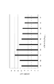
記憶素子3の各試料について、記憶層17のCo−Fe合金の組成と、飽和磁化量Ms及び実効的な反磁界の大きさMeffectiveの測定結果、さらに飽和磁化量と実効的な反磁界の大きさとの比Meffective/Msを表1に示す。ここで、表1に記載の記憶層17のCo−Fe合金のCo量は原子%で示している。
For each sample of the
表1から、CoxFe100-xのCo量xが70%以下の場合において、実効的な反磁界の大きさ(Meffective)は飽和磁化量Msよりも小さく、つまり、Co量xが70%以下のときの比Meffective/Msは1.0より小さな値になっている。
さらに、Co量xが20%となるまでは、Co量xが小さくなるほどMeffective/Msの値は小さくなるが、さらにCo量を減少させるとこの比の値がやや増加することが確認できる。
From Table 1, when the Co amount x of Co x Fe 100-x is 70% or less, the effective demagnetizing field magnitude (Meffective) is smaller than the saturation magnetization amount Ms, that is, the Co amount x is 70%. The ratio Meffective / Ms in the following cases is a value smaller than 1.0.
Further, until the Co amount x reaches 20%, the value of Meffective / Ms decreases as the Co amount x decreases, but it can be confirmed that the value of this ratio slightly increases when the Co amount is further decreased.
反転電流値の測定結果を図3に示し、熱安定性の指標の測定結果を図4に示す。
図3は、記憶層17のCo−Fe合金のCo量(CoFe中の含有量;原子%)と、反転電流値から求めた反転電流密度Jc0との関係を示している。
図4は、記憶層17のCo−Fe合金のCo量(CoFe中の含有量;原子%)と、熱安定性の指標Δ(KV/kBT)との関係を示している。
The measurement result of the inversion current value is shown in FIG. 3, and the measurement result of the thermal stability index is shown in FIG.
FIG. 3 shows the relationship between the amount of Co in the Co—Fe alloy of the memory layer 17 (content in CoFe; atomic%) and the reversal current density Jc0 obtained from the reversal current value.
FIG. 4 shows the relationship between the Co content (content in CoFe; atomic%) of the Co—Fe alloy of the memory layer 17 and the thermal stability index Δ (KV / k B T).
図3より、Co量xが70%以下の場合においては、Co量xが小さくになるにつれて、反転電流密度Jc0が小さくなっていくことがわかる。
これは、Co量xが小さくなった場合、飽和磁化量Msは増加するが実効的な反磁界Meffectiveが小さくなるために、両者の積(Ms×Meffective)としては小さくなることに起因する。
FIG. 3 shows that when the Co amount x is 70% or less, the inversion current density Jc0 decreases as the Co amount x decreases.
This is because when the Co amount x decreases, the saturation magnetization amount Ms increases, but the effective demagnetizing field Meffective decreases, so that the product of both (Ms × Meffective) decreases.
図4より、Co量xが小さくなるにつれて、熱安定性の指標Δ(=KV/kBT)が大きくなっていき、Co量xが70%以下になると熱安定性の指標Δが大きい値で安定することが分かる。
これは、図4に示した飽和磁化量Msの測定結果と、式(2)より熱安定性の指標Δが飽和磁化量Msに比例することとから予想される変化とよく一致している。
From FIG. 4, as the Co amount x decreases, the thermal stability index Δ (= KV / k B T) increases, and when the Co amount x becomes 70% or less, the thermal stability index Δ increases. It turns out to be stable.
This agrees well with the change expected from the measurement result of the saturation magnetization amount Ms shown in FIG. 4 and the fact that the thermal stability index Δ is proportional to the saturation magnetization amount Ms from the equation (2).
表1、図3、図4の結果より、実効的な反磁界Meffectiveが飽和磁化量Msよりも小さくなるCo量xが70%以下の組成において、Msを下げるといった熱安定性を犠牲にする手法を用いずに、高い熱安定性を有したまま、反転電流値Jc0を低減できることが明らかになった。 From the results of Table 1, FIG. 3 and FIG. 4, a method of sacrificing thermal stability such as lowering Ms in a composition in which the effective demagnetizing field Meffective is smaller than the saturation magnetization Ms and the Co content x is 70% or less. It was revealed that the reversal current value Jc0 can be reduced while maintaining high thermal stability without using.
[実験2]
上記[実験1]により、CoxFe100-xの場合、Co量xが70%以下の組成で高い熱安定性を有したまま、反転電流値Jc0を低減できることがわかった。
そこで、[実験2]においては、Co−Fe合金への、異種元素の添加効果を調べるため、B(ホウ素)を添加し、(Co50Fe50)92B8という組成の記録層17を用い、これがMeffective/Msにどのような影響を与えるかを調べた。試料の詳細は[実験1]と同様である。
[Experiment 2]
From the above [Experiment 1], it was found that in the case of Co x Fe 100-x , the reversal current value Jc0 can be reduced while maintaining high thermal stability with a composition in which the Co amount x is 70% or less.
Therefore, in [Experiment 2], in order to investigate the effect of adding different elements to the Co—Fe alloy, B (boron) is added, and the recording layer 17 having a composition of (Co 50 Fe 50 ) 92 B 8 is used. The effect of this on Meffective / Ms was investigated. The details of the sample are the same as those in [Experiment 1].
この結果、(Co50Fe50)92B8において、飽和磁化量Ms及び実効的な反磁界の大きさMeffectiveの値はそれぞれ1550(emu/cc)、950(emu/cc)となり、飽和磁化量と実効的な反磁界の大きさとの比Meffective/Msの値は0.61となった。 As a result, in (Co 50 Fe 50 ) 92 B 8 , the values of the saturation magnetization Ms and the effective demagnetizing field magnitude Meffective are 1550 (emu / cc) and 950 (emu / cc), respectively. The ratio of the effective demagnetizing field ratio Meffective / Ms was 0.61.
すなわち、8原子%のホウ素を添加しても、飽和磁化量Msと実効的な反磁界Meffectiveの大小関係はCoとFeの比で決定されることが明らかになった。
従って、記録層17の飽和磁化量Msを実効的な反磁界Meffectiveより小さくすることを、異種元素の添加が妨げることはないと考えられる。すなわち、高いトンネル磁気抵抗効果を発生させる、あるいは界面を平坦にして絶縁耐圧を向上させる、などの目的により、ホウ素などの添加元素を加えることも可能である。
That is, it has been clarified that even when 8 atomic% of boron is added, the magnitude relationship between the saturation magnetization Ms and the effective demagnetizing field Meffective is determined by the ratio of Co and Fe.
Therefore, it is considered that the addition of the different element does not prevent the saturation magnetization amount Ms of the recording layer 17 from being smaller than the effective demagnetizing field Meffective. That is, an additive element such as boron can be added for the purpose of generating a high tunnel magnetoresistance effect or improving the dielectric strength by flattening the interface.
[実験3]
Gbitクラスのスピン注入型メモリでは、記録素子のサイズが100nmφ以下になることが想定される。そこで、[実験3]において、50nmφのサイズの記憶素子を用いて、熱安定性を評価した。
Co−Fe合金の組成は、CoFe中のCoの組成比x(原子%)を、90%、80%、70%、60%、50%、40%、30%、20%、10%、0%と変化させた。
素子サイズ以外の試料の詳細は[実験1]と同様である。
[Experiment 3]
In the Gbit class spin injection type memory, the size of the recording element is assumed to be 100 nmφ or less. Therefore, in [Experiment 3], thermal stability was evaluated using a memory element having a size of 50 nmφ.
The composition of the Co—Fe alloy is such that the Co composition ratio x (atomic%) in CoFe is 90%, 80%, 70%, 60%, 50%, 40%, 30%, 20%, 10%, 0 %.
Details of the sample other than the element size are the same as those in [Experiment 1].
記憶素子3のサイズが50nmφの場合のCo−Fe合金のCo量(CoFe中の含有量;原子%)と熱安定性の指標Δ(KV/kBT)の関係を図5に示す。
FIG. 5 shows the relationship between the Co content of Co—Fe alloy (content in CoFe; atomic%) and the thermal stability index Δ (KV / k B T) when the size of the
図5より、素子サイズが50nmφになったことにより、熱安定性指数ΔのCo−Fe合金組成依存性が図4に示した短軸0.09μm×長軸0.18μmの楕円形状記憶素子で得られたΔのCo−Fe合金組成依存性から大きく変化したことが分かる。
図5によると、Coが40%以下、すなわちFeが60%以上存在するCo−Fe合金組成の場合にのみ、高い熱安定性が保持されている。
種々の検討を行った結果、Feが60%以上存在するCo−Fe合金が極微小な記憶素子において高い熱安定性Δを示す理由は、Co−Fe合金の磁化が膜面垂直方向を向いていることに起因していることが明らかになった。(外部磁界がない場合に磁化が安定になる方向は容易軸方向と呼ばれ、記憶素子の抵抗の外部磁界依存を測定し、その際の磁界方向を面内方向と垂直方向で比較することで調べることが可能である)。
Co−Fe合金の磁化が膜面垂直方向になっている理由は飽和磁化量Msが実効的な反磁界Meffectiveより著しく小さい組成であることに起因していると思われる。
また、垂直磁化膜になると極微小素子においても熱安定性が保たれる理由は、式(2)中のHk[実効的な異方性磁界]に関係しており、垂直磁化膜のHkは一般的に面内磁化膜よりも遥かに大きな値になる。つまり、垂直磁化膜では、大きなHkの効果により、面内磁化膜では十分な熱安定性Δを確保できない極微小な素子においても高い熱安定性Δを保つことが出来る。
上記の実験結果から、Co−Fe合金では、Fe量が60%以上になる場合、GbitクラスのST−MRAMに好適となるといえる。
As shown in FIG. 5, the element size is 50 nmφ, so that the dependence of the thermal stability index Δ on the Co—Fe alloy composition is 0.09 μm in the minor axis × 0.18 μm in the major axis shown in FIG. It turns out that it changed greatly from Co-Fe alloy composition dependence of obtained Δ.
According to FIG. 5, high thermal stability is maintained only in the case of a Co—Fe alloy composition in which Co is 40% or less, that is, Fe is 60% or more.
As a result of various investigations, the reason why the Co—Fe alloy containing 60% or more of Fe exhibits high thermal stability Δ in a very small memory element is that the magnetization of the Co—Fe alloy is directed in the direction perpendicular to the film surface. It became clear that it was caused by being. (The direction in which magnetization stabilizes in the absence of an external magnetic field is called the easy axis direction. By measuring the dependence of the resistance of the memory element on the external magnetic field, the magnetic field direction at that time is compared with the in-plane direction and the vertical direction. Can be investigated).
The reason why the magnetization of the Co—Fe alloy is in the direction perpendicular to the film surface seems to be due to the fact that the saturation magnetization Ms has a composition that is significantly smaller than the effective demagnetizing field Meffective.
In addition, the reason why the thermal stability is maintained even in a microelement when it is a perpendicular magnetization film is related to Hk [effective anisotropic magnetic field] in Equation (2), and the Hk of the perpendicular magnetization film is Generally, the value is much larger than that of the in-plane magnetization film. That is, in the perpendicular magnetization film, due to the effect of large Hk, high thermal stability Δ can be maintained even in a very small element that cannot secure sufficient thermal stability Δ in the in-plane magnetization film.
From the above experimental results, it can be said that the Co—Fe alloy is suitable for the Gbit class ST-MRAM when the Fe amount is 60% or more.
[実験4]
上記[実験3]により、組成式CoxFe100-xであらわされるCo−Fe合金において、Co量xが40%以下になる場合に、GbitクラスのST−MRAMに好適となることを示した。
そこで、[実験4]においては、Co−Fe合金への、異種元素の添加効果を調べるため、B(ホウ素)を添加し、(Co30Fe70)92B8という組成の記憶層17を有し、かつ50nmφのサイズの記憶素子を作製し、熱安定性を評価した。素子サイズ、組成以外の試料の詳細は[実験1]と同様である。
[Experiment 4]
[Experiment 3] shows that in a Co—Fe alloy represented by the composition formula Co x Fe 100-x , when the Co amount x is 40% or less, it is suitable for a Gbit class ST-MRAM. .
Therefore, in [Experiment 4], in order to investigate the effect of addition of different elements to the Co—Fe alloy, B (boron) is added, and the memory layer 17 having the composition of (Co 30 Fe 70 ) 92 B 8 is provided. In addition, a memory element having a size of 50 nmφ was manufactured, and thermal stability was evaluated. Details of the sample other than the element size and composition are the same as those in [Experiment 1].
この結果、(Co30Fe70)92B8において、熱安定性の指標であるΔの値は42となった。また、この記憶素子における磁化は膜面垂直方向を向いていることも明らかになった。 As a result, in (Co 30 Fe 70 ) 92 B 8 , the value of Δ, which is an index of thermal stability, was 42. It has also been clarified that the magnetization in this memory element is oriented in the direction perpendicular to the film surface.
すなわち、8原子%のホウ素を添加しても、熱安定性はCoとFeの組成でほぼ決定されることが明らかになり、これは磁化容易軸が膜面垂直となっていることに起因すると考えられる。
従って、Co−Fe合金の組成を調整し、Coを40%以下とすることで記憶素子の熱安定性を向上させることは、異種元素の添加により妨げられることはないと考えられる。すなわち、高いトンネル磁気抵抗効果を発生させる、あるいは界面を平坦にして絶縁耐圧を向上させる、などの目的により、ホウ素などの添加元素を加えることも可能である。
That is, it is clear that even when 8 atomic% boron is added, the thermal stability is almost determined by the composition of Co and Fe, which is due to the fact that the easy axis of magnetization is perpendicular to the film surface. Conceivable.
Therefore, adjusting the composition of the Co—Fe alloy and reducing the Co content to 40% or less can be considered not to be hindered by the addition of different elements. That is, an additive element such as boron can be added for the purpose of generating a high tunnel magnetoresistance effect or improving the dielectric strength by flattening the interface.
以上実施の形態について説明してきたが、本発明では、上述の各実施の形態で示した記憶素子3,20の膜構成に限らず、様々な膜構成を採用することが可能である。
例えば実施の形態では、磁化固定層15をCoFeBとしたが、実施の形態に限定されるものではなく、本発明の要旨を逸脱しない範囲でその他様々な構成が取り得る。
また、実施の形態では、単一の下地、キャップ材料、記憶素子形状しか示していないが、それらに限定されるものではなく、本発明の要旨を逸脱しない範囲でその他様々な構成が取り得る。
Although the embodiments have been described above, the present invention is not limited to the film configurations of the
For example, in the embodiment, the magnetization fixed
In the embodiments, only a single base, cap material, and memory element shape are shown, but the present invention is not limited to them, and various other configurations can be taken without departing from the gist of the present invention.
また実施の形態では、磁化固定層15は単層であったが、2層の強磁性層と非磁性層から成る積層フェリピン構造を用いても良い。また、さらに、積層フェリピン構造膜に反強磁性膜を付与した構造でもよい。
また、記憶素子の膜構成は、記憶層が磁化固定層の上側に配置される構成でも、下側に配置される構成でも全く問題はない。さらには、固定層が記録層の上下に存在する、いわゆるデュアル構造でも全く問題ない。
In the embodiment, the magnetization fixed
In addition, the film configuration of the storage element has no problem whether the storage layer is disposed above the magnetization fixed layer or the lower layer. Furthermore, there is no problem at all even in a so-called dual structure in which the fixed layer exists above and below the recording layer.
3 記憶素子、14 下地層、15 磁化固定層、16 中間層、17 記憶層、18 キャップ層 3 memory element, 14 underlayer, 15 magnetization fixed layer, 16 intermediate layer, 17 memory layer, 18 cap layer
Claims (5)
上記記憶層に記憶された情報の基準となる磁化を有する磁化固定層と、
上記記憶層と上記磁化固定層の間に設けられる非磁性体による中間層と、
を有し、
上記記憶層、上記中間層、上記磁化固定層を有する層構造の積層方向に流れる電流に伴って発生するスピントルク磁化反転を利用して上記記憶層の磁化を反転させることにより情報の記憶を行うとともに、
上記記憶層は、Fe、Coの少なくとも一方を含有する合金領域を含み、
上記記憶層がその磁化反転過程で受ける実効的な反磁界の大きさが、上記記憶層の飽和磁化量よりも小さい記憶素子。 A storage layer that holds information by the magnetization state of the magnetic material;
A magnetization fixed layer having a magnetization serving as a reference for information stored in the storage layer;
A nonmagnetic intermediate layer provided between the storage layer and the magnetization fixed layer;
Have
Information is stored by reversing the magnetization of the storage layer by utilizing the spin torque magnetization reversal that occurs with the current flowing in the stacking direction of the layer structure having the storage layer, the intermediate layer, and the magnetization fixed layer. With
The memory layer includes an alloy region containing at least one of Fe and Co,
A storage element in which the effective demagnetizing field that the storage layer receives in the magnetization reversal process is smaller than the saturation magnetization of the storage layer.
互いに交差する2種類の配線とを備え、
上記記憶素子は、
情報を磁性体の磁化状態により保持する記憶層と、上記記憶層に記憶された情報の基準となる磁化を有する磁化固定層と、上記記憶層と上記磁化固定層の間に設けられる非磁性体による中間層とを有し、上記記憶層、上記中間層、上記磁化固定層を有する層構造の積層方向に流れる電流に伴って発生するスピントルク磁化反転を利用して上記記憶層の磁化を反転させることにより情報の記憶を行うとともに、上記記憶層はFe、Coの少なくとも一方を含有する合金領域を含み、上記記憶層がその磁化反転過程で受ける実効的な反磁界の大きさが、上記記憶層の飽和磁化量よりも小さい構成とされ、
上記2種類の配線の間に上記記憶素子が配置され、
上記2種類の配線を通じて、上記記憶素子に上記積層方向の電流が流れ、これに伴ってスピントルク磁化反転が起こる記憶装置。 A storage element that holds information according to the magnetization state of the magnetic material;
Two types of wiring intersecting each other,
The memory element is
A storage layer that retains information according to the magnetization state of the magnetic material, a magnetization fixed layer having a magnetization serving as a reference for information stored in the storage layer, and a nonmagnetic material provided between the storage layer and the magnetization fixed layer And reversing the magnetization of the storage layer by utilizing spin torque magnetization reversal that occurs with the current flowing in the stacking direction of the layer structure having the storage layer, the intermediate layer, and the fixed magnetization layer. Information is stored, and the storage layer includes an alloy region containing at least one of Fe and Co, and the effective demagnetizing field received by the storage layer during the magnetization reversal process is It is configured to be smaller than the saturation magnetization of the layer,
The memory element is disposed between the two types of wirings,
A memory device in which a current in the stacking direction flows in the memory element through the two types of wirings, and accordingly, spin torque magnetization reversal occurs.
Priority Applications (6)
| Application Number | Priority Date | Filing Date | Title |
|---|---|---|---|
| JP2010196418A JP2012054439A (en) | 2010-09-02 | 2010-09-02 | Storage element and storage device |
| TW100129116A TW201222546A (en) | 2010-09-02 | 2011-08-15 | Memory element and memory device |
| KR1020110084330A KR20120023560A (en) | 2010-09-02 | 2011-08-24 | Memory element and memory device |
| US13/217,925 US8750035B2 (en) | 2010-09-02 | 2011-08-25 | Memory element and memory device |
| CN2011102497759A CN102385923A (en) | 2010-09-02 | 2011-08-26 | Memory element and memory device |
| US14/263,657 US9299916B2 (en) | 2010-09-02 | 2014-04-28 | Memory element and memory device |
Applications Claiming Priority (1)
| Application Number | Priority Date | Filing Date | Title |
|---|---|---|---|
| JP2010196418A JP2012054439A (en) | 2010-09-02 | 2010-09-02 | Storage element and storage device |
Publications (2)
| Publication Number | Publication Date |
|---|---|
| JP2012054439A true JP2012054439A (en) | 2012-03-15 |
| JP2012054439A5 JP2012054439A5 (en) | 2013-09-19 |
Family
ID=45770637
Family Applications (1)
| Application Number | Title | Priority Date | Filing Date |
|---|---|---|---|
| JP2010196418A Pending JP2012054439A (en) | 2010-09-02 | 2010-09-02 | Storage element and storage device |
Country Status (5)
| Country | Link |
|---|---|
| US (2) | US8750035B2 (en) |
| JP (1) | JP2012054439A (en) |
| KR (1) | KR20120023560A (en) |
| CN (1) | CN102385923A (en) |
| TW (1) | TW201222546A (en) |
Families Citing this family (5)
| Publication number | Priority date | Publication date | Assignee | Title |
|---|---|---|---|---|
| JP5786341B2 (en) | 2010-09-06 | 2015-09-30 | ソニー株式会社 | Memory element and memory device |
| JP5742142B2 (en) * | 2010-09-08 | 2015-07-01 | ソニー株式会社 | Memory element and memory device |
| JP2012064623A (en) * | 2010-09-14 | 2012-03-29 | Sony Corp | Storage element and memory unit |
| CN102637939B (en) * | 2012-04-28 | 2014-06-11 | 中国科学院苏州纳米技术与纳米仿生研究所 | Spinning microwave oscillator based on vertical magnetizing free layer and manufacturing method thereof |
| KR102433703B1 (en) * | 2015-11-30 | 2022-08-19 | 에스케이하이닉스 주식회사 | Electronic device |
Citations (9)
| Publication number | Priority date | Publication date | Assignee | Title |
|---|---|---|---|---|
| JP2007294737A (en) * | 2006-04-26 | 2007-11-08 | Hitachi Ltd | Tunnel magnetoresistance effect element, and magnetic memory cell and magnetic random access memory using the same |
| JP2008010590A (en) * | 2006-06-28 | 2008-01-17 | Toshiba Corp | Magnetoresistive element, and magnetic memory |
| JP2008227388A (en) * | 2007-03-15 | 2008-09-25 | Sony Corp | Memory element and memory |
| JP2009081315A (en) * | 2007-09-26 | 2009-04-16 | Toshiba Corp | Magnetoresistive element, and magnetic memory |
| JP2009081216A (en) * | 2007-09-25 | 2009-04-16 | Toshiba Corp | Magnetoresistance effect element and magnetic random access memory using the same |
| JP2009081215A (en) * | 2007-09-25 | 2009-04-16 | Toshiba Corp | Magnetoresistive effect element and magnetic random access memory using the same |
| JP2009094104A (en) * | 2007-10-03 | 2009-04-30 | Toshiba Corp | Magnetoresistive element |
| JP2009151835A (en) * | 2007-12-18 | 2009-07-09 | Toshiba Corp | Magnetic random access memory and its writing method |
| JP2010016408A (en) * | 2009-10-19 | 2010-01-21 | Toshiba Corp | Magnetoresistive element and magnetic memory |
Family Cites Families (8)
| Publication number | Priority date | Publication date | Assignee | Title |
|---|---|---|---|---|
| US6130814A (en) | 1998-07-28 | 2000-10-10 | International Business Machines Corporation | Current-induced magnetic switching device and memory including the same |
| JP2002329905A (en) * | 2001-05-02 | 2002-11-15 | Fujitsu Ltd | Cpp-structure magnetoresistance effect element and method of manufacturing the same |
| JP2003017782A (en) | 2001-07-04 | 2003-01-17 | Rikogaku Shinkokai | Carrier spin injected inverted magnetization magnetoresistive effect film, non-volatile memory element using the film, and memory device using the element |
| WO2004055906A1 (en) * | 2002-12-13 | 2004-07-01 | Japan Science And Technology Agency | Spin injection device, magnetic device using the same, magnetic thin film used in the same |
| US6845038B1 (en) * | 2003-02-01 | 2005-01-18 | Alla Mikhailovna Shukh | Magnetic tunnel junction memory device |
| US7242045B2 (en) | 2004-02-19 | 2007-07-10 | Grandis, Inc. | Spin transfer magnetic element having low saturation magnetization free layers |
| US7576956B2 (en) * | 2004-07-26 | 2009-08-18 | Grandis Inc. | Magnetic tunnel junction having diffusion stop layer |
| JP4277870B2 (en) * | 2006-04-17 | 2009-06-10 | ソニー株式会社 | Storage element and memory |
-
2010
- 2010-09-02 JP JP2010196418A patent/JP2012054439A/en active Pending
-
2011
- 2011-08-15 TW TW100129116A patent/TW201222546A/en unknown
- 2011-08-24 KR KR1020110084330A patent/KR20120023560A/en not_active Application Discontinuation
- 2011-08-25 US US13/217,925 patent/US8750035B2/en not_active Expired - Fee Related
- 2011-08-26 CN CN2011102497759A patent/CN102385923A/en active Pending
-
2014
- 2014-04-28 US US14/263,657 patent/US9299916B2/en active Active
Patent Citations (9)
| Publication number | Priority date | Publication date | Assignee | Title |
|---|---|---|---|---|
| JP2007294737A (en) * | 2006-04-26 | 2007-11-08 | Hitachi Ltd | Tunnel magnetoresistance effect element, and magnetic memory cell and magnetic random access memory using the same |
| JP2008010590A (en) * | 2006-06-28 | 2008-01-17 | Toshiba Corp | Magnetoresistive element, and magnetic memory |
| JP2008227388A (en) * | 2007-03-15 | 2008-09-25 | Sony Corp | Memory element and memory |
| JP2009081216A (en) * | 2007-09-25 | 2009-04-16 | Toshiba Corp | Magnetoresistance effect element and magnetic random access memory using the same |
| JP2009081215A (en) * | 2007-09-25 | 2009-04-16 | Toshiba Corp | Magnetoresistive effect element and magnetic random access memory using the same |
| JP2009081315A (en) * | 2007-09-26 | 2009-04-16 | Toshiba Corp | Magnetoresistive element, and magnetic memory |
| JP2009094104A (en) * | 2007-10-03 | 2009-04-30 | Toshiba Corp | Magnetoresistive element |
| JP2009151835A (en) * | 2007-12-18 | 2009-07-09 | Toshiba Corp | Magnetic random access memory and its writing method |
| JP2010016408A (en) * | 2009-10-19 | 2010-01-21 | Toshiba Corp | Magnetoresistive element and magnetic memory |
Non-Patent Citations (3)
| Title |
|---|
| S.IKEDA(他9名): "A perpendicular-anisotropy CoFeB-MgO magnetic tunnel junction", NATURE MATERIALS, vol. 9, JPN6014033717, 11 July 2010 (2010-07-11), GB, pages 721 - 724, ISSN: 0002873087 * |
| S.ISHIBASHI(他10名): "Large Diode Sensitivity of CoFeB/MgO/CoFeB Magnetic Tunnel Junctions", APPLIED PHYSICS EXPRESS, vol. Volume 3, Number 7, 073001, JPN7015001415, 18 June 2010 (2010-06-18), US, pages 1 - 3, ISSN: 0003080467 * |
| S.YATAKA(他6名): "Influence of perpendicular magnetic anisotropy on spin-transfer switching current in CoFeB/MgO/CoFeB", JOURNAL OF APPLIED PHYSICS, vol. Volume 105, Issue 7, 07D131, JPN7015001414, 2009, US, pages 1 - 3, ISSN: 0003080466 * |
Also Published As
| Publication number | Publication date |
|---|---|
| KR20120023560A (en) | 2012-03-13 |
| US20120057403A1 (en) | 2012-03-08 |
| US9299916B2 (en) | 2016-03-29 |
| US20140231943A1 (en) | 2014-08-21 |
| TW201222546A (en) | 2012-06-01 |
| US8750035B2 (en) | 2014-06-10 |
| CN102385923A (en) | 2012-03-21 |
Similar Documents
| Publication | Publication Date | Title |
|---|---|---|
| US9324940B2 (en) | Storage element, memory and electronic apparatus | |
| JP4682998B2 (en) | Memory element and memory | |
| JP6244617B2 (en) | Storage element, storage device, magnetic head | |
| JP6194752B2 (en) | Storage element, storage device, magnetic head | |
| JP2012244031A (en) | Storage element and storage device | |
| JP2012059906A (en) | Storage element and memory unit | |
| JP5782715B2 (en) | Storage element and storage device | |
| JP2012146727A (en) | Storage element and storage device | |
| JP2012059808A (en) | Storage element and memory unit | |
| JP2012235015A (en) | Storage element and storage device | |
| JP5987613B2 (en) | Storage element, storage device, magnetic head | |
| KR101891829B1 (en) | Memory element and memory device | |
| WO2014050379A1 (en) | Storage element, storage device, and magnetic head | |
| JP2013033881A (en) | Storage element and storage device | |
| WO2013080436A1 (en) | Storage element, and storage device | |
| JP2012064623A (en) | Storage element and memory unit | |
| JP2012160681A (en) | Memory element, memory device | |
| US9299916B2 (en) | Memory element and memory device | |
| JP5742142B2 (en) | Memory element and memory device | |
| JP2012059878A (en) | Storage element and memory unit | |
| JP2012064624A (en) | Storage element and memory unit | |
| JP5724256B2 (en) | Memory element and memory device | |
| JP5803079B2 (en) | Memory element and memory device | |
| JP2012059809A (en) | Storage element and memory unit | |
| JP2017212464A (en) | Storage element, storage device, and magnetic head |
Legal Events
| Date | Code | Title | Description |
|---|---|---|---|
| A521 | Request for written amendment filed |
Free format text: JAPANESE INTERMEDIATE CODE: A523 Effective date: 20130812 |
|
| A621 | Written request for application examination |
Free format text: JAPANESE INTERMEDIATE CODE: A621 Effective date: 20130812 |
|
| A977 | Report on retrieval |
Free format text: JAPANESE INTERMEDIATE CODE: A971007 Effective date: 20140731 |
|
| A131 | Notification of reasons for refusal |
Free format text: JAPANESE INTERMEDIATE CODE: A131 Effective date: 20140819 |
|
| A521 | Request for written amendment filed |
Free format text: JAPANESE INTERMEDIATE CODE: A523 Effective date: 20141009 |
|
| A131 | Notification of reasons for refusal |
Free format text: JAPANESE INTERMEDIATE CODE: A131 Effective date: 20150106 |
|
| A521 | Request for written amendment filed |
Free format text: JAPANESE INTERMEDIATE CODE: A523 Effective date: 20150224 |
|
| A131 | Notification of reasons for refusal |
Free format text: JAPANESE INTERMEDIATE CODE: A131 Effective date: 20150526 |
|
| A521 | Request for written amendment filed |
Free format text: JAPANESE INTERMEDIATE CODE: A523 Effective date: 20150721 |
|
| A02 | Decision of refusal |
Free format text: JAPANESE INTERMEDIATE CODE: A02 Effective date: 20150818 |