JP2012019164A - Manufacturing method of plate with passage, plate with passage, temperature adjustment plate, cold plate, and shower plate - Google Patents
Manufacturing method of plate with passage, plate with passage, temperature adjustment plate, cold plate, and shower plate Download PDFInfo
- Publication number
- JP2012019164A JP2012019164A JP2010157235A JP2010157235A JP2012019164A JP 2012019164 A JP2012019164 A JP 2012019164A JP 2010157235 A JP2010157235 A JP 2010157235A JP 2010157235 A JP2010157235 A JP 2010157235A JP 2012019164 A JP2012019164 A JP 2012019164A
- Authority
- JP
- Japan
- Prior art keywords
- plate
- flow path
- gas
- lid
- groove
- Prior art date
- Legal status (The legal status is an assumption and is not a legal conclusion. Google has not performed a legal analysis and makes no representation as to the accuracy of the status listed.)
- Granted
Links
- 238000004519 manufacturing process Methods 0.000 title claims description 53
- 239000000843 powder Substances 0.000 claims abstract description 41
- 229910045601 alloy Inorganic materials 0.000 claims abstract description 32
- 239000000956 alloy Substances 0.000 claims abstract description 32
- 229910052751 metal Inorganic materials 0.000 claims abstract description 30
- 239000002184 metal Substances 0.000 claims abstract description 30
- 239000012530 fluid Substances 0.000 claims abstract description 18
- 239000007787 solid Substances 0.000 claims abstract description 8
- 238000005507 spraying Methods 0.000 claims abstract description 7
- 230000008021 deposition Effects 0.000 claims description 65
- 238000000034 method Methods 0.000 claims description 60
- 239000007921 spray Substances 0.000 claims description 18
- 229910000838 Al alloy Inorganic materials 0.000 claims description 17
- XAGFODPZIPBFFR-UHFFFAOYSA-N aluminium Chemical compound [Al] XAGFODPZIPBFFR-UHFFFAOYSA-N 0.000 claims description 17
- 229910052782 aluminium Inorganic materials 0.000 claims description 15
- 239000010936 titanium Substances 0.000 claims description 13
- 239000010949 copper Substances 0.000 claims description 11
- RTAQQCXQSZGOHL-UHFFFAOYSA-N Titanium Chemical compound [Ti] RTAQQCXQSZGOHL-UHFFFAOYSA-N 0.000 claims description 9
- 239000002826 coolant Substances 0.000 claims description 9
- 239000010935 stainless steel Substances 0.000 claims description 9
- 229910001220 stainless steel Inorganic materials 0.000 claims description 9
- 229910052719 titanium Inorganic materials 0.000 claims description 9
- RYGMFSIKBFXOCR-UHFFFAOYSA-N Copper Chemical compound [Cu] RYGMFSIKBFXOCR-UHFFFAOYSA-N 0.000 claims description 7
- 229910052802 copper Inorganic materials 0.000 claims description 7
- 229910001069 Ti alloy Inorganic materials 0.000 claims description 3
- 239000007790 solid phase Substances 0.000 claims 2
- 229910000881 Cu alloy Inorganic materials 0.000 claims 1
- 239000007789 gas Substances 0.000 description 121
- 238000000151 deposition Methods 0.000 description 57
- 238000010586 diagram Methods 0.000 description 25
- 239000000463 material Substances 0.000 description 20
- 239000000758 substrate Substances 0.000 description 20
- 230000015572 biosynthetic process Effects 0.000 description 11
- 238000012986 modification Methods 0.000 description 11
- 230000004048 modification Effects 0.000 description 11
- 238000005520 cutting process Methods 0.000 description 9
- 238000005219 brazing Methods 0.000 description 8
- 238000000605 extraction Methods 0.000 description 7
- 238000003466 welding Methods 0.000 description 7
- 238000010438 heat treatment Methods 0.000 description 5
- 238000005304 joining Methods 0.000 description 5
- 150000002739 metals Chemical class 0.000 description 5
- 239000013590 bulk material Substances 0.000 description 4
- 238000011109 contamination Methods 0.000 description 4
- 239000000853 adhesive Substances 0.000 description 3
- 230000001070 adhesive effect Effects 0.000 description 3
- 238000005229 chemical vapour deposition Methods 0.000 description 3
- 239000004973 liquid crystal related substance Substances 0.000 description 3
- 238000002844 melting Methods 0.000 description 3
- 230000008018 melting Effects 0.000 description 3
- 230000003287 optical effect Effects 0.000 description 3
- 238000007789 sealing Methods 0.000 description 3
- 239000004065 semiconductor Substances 0.000 description 3
- 238000007796 conventional method Methods 0.000 description 2
- 238000005260 corrosion Methods 0.000 description 2
- 230000007797 corrosion Effects 0.000 description 2
- 238000010894 electron beam technology Methods 0.000 description 2
- 238000002156 mixing Methods 0.000 description 2
- 238000005498 polishing Methods 0.000 description 2
- 239000002994 raw material Substances 0.000 description 2
- IJGRMHOSHXDMSA-UHFFFAOYSA-N Atomic nitrogen Chemical compound N#N IJGRMHOSHXDMSA-UHFFFAOYSA-N 0.000 description 1
- -1 aluminum (Al) Chemical class 0.000 description 1
- 238000009412 basement excavation Methods 0.000 description 1
- 238000005422 blasting Methods 0.000 description 1
- 238000001816 cooling Methods 0.000 description 1
- 238000006073 displacement reaction Methods 0.000 description 1
- 230000000694 effects Effects 0.000 description 1
- 239000000945 filler Substances 0.000 description 1
- 239000001307 helium Substances 0.000 description 1
- 229910052734 helium Inorganic materials 0.000 description 1
- SWQJXJOGLNCZEY-UHFFFAOYSA-N helium atom Chemical compound [He] SWQJXJOGLNCZEY-UHFFFAOYSA-N 0.000 description 1
- 239000011261 inert gas Substances 0.000 description 1
- 239000007788 liquid Substances 0.000 description 1
- 239000002609 medium Substances 0.000 description 1
- 230000009972 noncorrosive effect Effects 0.000 description 1
- 239000003960 organic solvent Substances 0.000 description 1
- 239000002245 particle Substances 0.000 description 1
- 230000000149 penetrating effect Effects 0.000 description 1
- 239000013535 sea water Substances 0.000 description 1
- 238000004904 shortening Methods 0.000 description 1
- XLYOFNOQVPJJNP-UHFFFAOYSA-N water Substances O XLYOFNOQVPJJNP-UHFFFAOYSA-N 0.000 description 1
Images


Classifications
-
- B—PERFORMING OPERATIONS; TRANSPORTING
- B23—MACHINE TOOLS; METAL-WORKING NOT OTHERWISE PROVIDED FOR
- B23P—METAL-WORKING NOT OTHERWISE PROVIDED FOR; COMBINED OPERATIONS; UNIVERSAL MACHINE TOOLS
- B23P15/00—Making specific metal objects by operations not covered by a single other subclass or a group in this subclass
- B23P15/26—Making specific metal objects by operations not covered by a single other subclass or a group in this subclass heat exchangers or the like
-
- C—CHEMISTRY; METALLURGY
- C23—COATING METALLIC MATERIAL; COATING MATERIAL WITH METALLIC MATERIAL; CHEMICAL SURFACE TREATMENT; DIFFUSION TREATMENT OF METALLIC MATERIAL; COATING BY VACUUM EVAPORATION, BY SPUTTERING, BY ION IMPLANTATION OR BY CHEMICAL VAPOUR DEPOSITION, IN GENERAL; INHIBITING CORROSION OF METALLIC MATERIAL OR INCRUSTATION IN GENERAL
- C23C—COATING METALLIC MATERIAL; COATING MATERIAL WITH METALLIC MATERIAL; SURFACE TREATMENT OF METALLIC MATERIAL BY DIFFUSION INTO THE SURFACE, BY CHEMICAL CONVERSION OR SUBSTITUTION; COATING BY VACUUM EVAPORATION, BY SPUTTERING, BY ION IMPLANTATION OR BY CHEMICAL VAPOUR DEPOSITION, IN GENERAL
- C23C16/00—Chemical coating by decomposition of gaseous compounds, without leaving reaction products of surface material in the coating, i.e. chemical vapour deposition [CVD] processes
- C23C16/44—Chemical coating by decomposition of gaseous compounds, without leaving reaction products of surface material in the coating, i.e. chemical vapour deposition [CVD] processes characterised by the method of coating
- C23C16/455—Chemical coating by decomposition of gaseous compounds, without leaving reaction products of surface material in the coating, i.e. chemical vapour deposition [CVD] processes characterised by the method of coating characterised by the method used for introducing gases into reaction chamber or for modifying gas flows in reaction chamber
- C23C16/45563—Gas nozzles
- C23C16/45565—Shower nozzles
-
- C—CHEMISTRY; METALLURGY
- C23—COATING METALLIC MATERIAL; COATING MATERIAL WITH METALLIC MATERIAL; CHEMICAL SURFACE TREATMENT; DIFFUSION TREATMENT OF METALLIC MATERIAL; COATING BY VACUUM EVAPORATION, BY SPUTTERING, BY ION IMPLANTATION OR BY CHEMICAL VAPOUR DEPOSITION, IN GENERAL; INHIBITING CORROSION OF METALLIC MATERIAL OR INCRUSTATION IN GENERAL
- C23C—COATING METALLIC MATERIAL; COATING MATERIAL WITH METALLIC MATERIAL; SURFACE TREATMENT OF METALLIC MATERIAL BY DIFFUSION INTO THE SURFACE, BY CHEMICAL CONVERSION OR SUBSTITUTION; COATING BY VACUUM EVAPORATION, BY SPUTTERING, BY ION IMPLANTATION OR BY CHEMICAL VAPOUR DEPOSITION, IN GENERAL
- C23C16/00—Chemical coating by decomposition of gaseous compounds, without leaving reaction products of surface material in the coating, i.e. chemical vapour deposition [CVD] processes
- C23C16/44—Chemical coating by decomposition of gaseous compounds, without leaving reaction products of surface material in the coating, i.e. chemical vapour deposition [CVD] processes characterised by the method of coating
- C23C16/458—Chemical coating by decomposition of gaseous compounds, without leaving reaction products of surface material in the coating, i.e. chemical vapour deposition [CVD] processes characterised by the method of coating characterised by the method used for supporting substrates in the reaction chamber
- C23C16/4582—Rigid and flat substrates, e.g. plates or discs
- C23C16/4583—Rigid and flat substrates, e.g. plates or discs the substrate being supported substantially horizontally
- C23C16/4586—Elements in the interior of the support, e.g. electrodes, heating or cooling devices
-
- C—CHEMISTRY; METALLURGY
- C23—COATING METALLIC MATERIAL; COATING MATERIAL WITH METALLIC MATERIAL; CHEMICAL SURFACE TREATMENT; DIFFUSION TREATMENT OF METALLIC MATERIAL; COATING BY VACUUM EVAPORATION, BY SPUTTERING, BY ION IMPLANTATION OR BY CHEMICAL VAPOUR DEPOSITION, IN GENERAL; INHIBITING CORROSION OF METALLIC MATERIAL OR INCRUSTATION IN GENERAL
- C23C—COATING METALLIC MATERIAL; COATING MATERIAL WITH METALLIC MATERIAL; SURFACE TREATMENT OF METALLIC MATERIAL BY DIFFUSION INTO THE SURFACE, BY CHEMICAL CONVERSION OR SUBSTITUTION; COATING BY VACUUM EVAPORATION, BY SPUTTERING, BY ION IMPLANTATION OR BY CHEMICAL VAPOUR DEPOSITION, IN GENERAL
- C23C24/00—Coating starting from inorganic powder
- C23C24/02—Coating starting from inorganic powder by application of pressure only
- C23C24/04—Impact or kinetic deposition of particles
-
- F—MECHANICAL ENGINEERING; LIGHTING; HEATING; WEAPONS; BLASTING
- F28—HEAT EXCHANGE IN GENERAL
- F28F—DETAILS OF HEAT-EXCHANGE AND HEAT-TRANSFER APPARATUS, OF GENERAL APPLICATION
- F28F3/00—Plate-like or laminated elements; Assemblies of plate-like or laminated elements
- F28F3/12—Elements constructed in the shape of a hollow panel, e.g. with channels
-
- H—ELECTRICITY
- H01—ELECTRIC ELEMENTS
- H01L—SEMICONDUCTOR DEVICES NOT COVERED BY CLASS H10
- H01L21/00—Processes or apparatus adapted for the manufacture or treatment of semiconductor or solid state devices or of parts thereof
- H01L21/67—Apparatus specially adapted for handling semiconductor or electric solid state devices during manufacture or treatment thereof; Apparatus specially adapted for handling wafers during manufacture or treatment of semiconductor or electric solid state devices or components ; Apparatus not specifically provided for elsewhere
- H01L21/67005—Apparatus not specifically provided for elsewhere
- H01L21/67011—Apparatus for manufacture or treatment
- H01L21/67098—Apparatus for thermal treatment
- H01L21/67109—Apparatus for thermal treatment mainly by convection
-
- H—ELECTRICITY
- H01—ELECTRIC ELEMENTS
- H01L—SEMICONDUCTOR DEVICES NOT COVERED BY CLASS H10
- H01L21/00—Processes or apparatus adapted for the manufacture or treatment of semiconductor or solid state devices or of parts thereof
- H01L21/67—Apparatus specially adapted for handling semiconductor or electric solid state devices during manufacture or treatment thereof; Apparatus specially adapted for handling wafers during manufacture or treatment of semiconductor or electric solid state devices or components ; Apparatus not specifically provided for elsewhere
- H01L21/683—Apparatus specially adapted for handling semiconductor or electric solid state devices during manufacture or treatment thereof; Apparatus specially adapted for handling wafers during manufacture or treatment of semiconductor or electric solid state devices or components ; Apparatus not specifically provided for elsewhere for supporting or gripping
-
- F—MECHANICAL ENGINEERING; LIGHTING; HEATING; WEAPONS; BLASTING
- F28—HEAT EXCHANGE IN GENERAL
- F28F—DETAILS OF HEAT-EXCHANGE AND HEAT-TRANSFER APPARATUS, OF GENERAL APPLICATION
- F28F2220/00—Closure means, e.g. end caps on header boxes or plugs on conduits
-
- Y—GENERAL TAGGING OF NEW TECHNOLOGICAL DEVELOPMENTS; GENERAL TAGGING OF CROSS-SECTIONAL TECHNOLOGIES SPANNING OVER SEVERAL SECTIONS OF THE IPC; TECHNICAL SUBJECTS COVERED BY FORMER USPC CROSS-REFERENCE ART COLLECTIONS [XRACs] AND DIGESTS
- Y10—TECHNICAL SUBJECTS COVERED BY FORMER USPC
- Y10T—TECHNICAL SUBJECTS COVERED BY FORMER US CLASSIFICATION
- Y10T29/00—Metal working
- Y10T29/49—Method of mechanical manufacture
- Y10T29/4935—Heat exchanger or boiler making
Landscapes
- Chemical & Material Sciences (AREA)
- Engineering & Computer Science (AREA)
- Mechanical Engineering (AREA)
- Chemical Kinetics & Catalysis (AREA)
- Materials Engineering (AREA)
- Metallurgy (AREA)
- Organic Chemistry (AREA)
- Physics & Mathematics (AREA)
- General Chemical & Material Sciences (AREA)
- Microelectronics & Electronic Packaging (AREA)
- Condensed Matter Physics & Semiconductors (AREA)
- General Physics & Mathematics (AREA)
- Manufacturing & Machinery (AREA)
- Computer Hardware Design (AREA)
- Power Engineering (AREA)
- General Engineering & Computer Science (AREA)
- Thermal Sciences (AREA)
- Other Surface Treatments For Metallic Materials (AREA)
- Chemical Vapour Deposition (AREA)
- Heat-Exchange Devices With Radiators And Conduit Assemblies (AREA)
Abstract
Description
本発明は、半導体や液晶表示装置や光ディスク等の製造プロセスにおいて、基板の温度やガス供給等に用いられる流路付きプレートの製造方法、流路付きプレート、温度調節プレート、コールドプレート、及びシャワープレートに関するものである。 The present invention relates to a method of manufacturing a plate with a flow path used for substrate temperature, gas supply, etc. in a manufacturing process of a semiconductor, a liquid crystal display device, an optical disk, etc., a plate with a flow path, a temperature control plate, a cold plate, and a shower plate It is about.
半導体や液晶表示装置や光ディスク等の製造における種々の基板プロセスにおいては、基板の温度を調節する温度調節プレート(コールドプレート等)や、基板に所定の成分を有するガスを供給するシャワープレートが用いられている。これらの温度調節プレートやシャワープレートは、一般的に、アルミニウム又はアルミニウム合金等の金属プレートの内部に熱媒体やガスを流通させる流路を設けた構造を有している(例えば、特許文献1〜3参照)。
In various substrate processes in the manufacture of semiconductors, liquid crystal display devices, optical disks, etc., temperature control plates (such as cold plates) that adjust the temperature of the substrate and shower plates that supply a gas having a predetermined component to the substrate are used. ing. These temperature control plates and shower plates generally have a structure in which a flow path for circulating a heat medium or gas is provided inside a metal plate such as aluminum or aluminum alloy (for example,
このような流路付きプレートは、従来、金属プレート本体に掘削加工等によって流路を形成し、この流路を封止する別の金属プレート(例えば、押え板)を上記金属プレート本体の流路側に重ね、溶接加工やロウ付或いは接着剤により両者を接合又は接着することにより製造されていた。 Such a plate with a flow path is conventionally formed by forming a flow path in the metal plate main body by excavation or the like, and another metal plate (for example, a holding plate) for sealing the flow path is connected to the flow path side of the metal plate main body. It was manufactured by joining the two together by welding, brazing, or adhesive.
しかしながら、このような従来の製造方法によれば、ロウ材のセットやロウ付時間、或いは溶接のためのフィラーのセットに時間がかかるため、多くの製造工数を要してしまう。また、溶接においては、高温の熱が母材に加わるため、熱歪みに起因する目違いやアンダーカットや母材の反り等により、流路にリークが生じるおそれがある。一方、ロウ付や接着剤を用いる場合には、ロウ材等の母材以外の成分が流路に流れ込み、流路の汚染を招くおそれがある。 However, according to such a conventional manufacturing method, since it takes time to set a brazing material, brazing time, or set a filler for welding, a large number of manufacturing steps are required. Further, in welding, since high-temperature heat is applied to the base material, there is a possibility that leakage may occur in the flow path due to misinterpretation due to thermal distortion, undercutting, warpage of the base material, or the like. On the other hand, when brazing or an adhesive is used, components other than the base material such as brazing material may flow into the flow path, leading to contamination of the flow path.
本発明は、上記に鑑みてなされたものであって、従来よりも製造工程に要する時間を短縮でき、且つ流路のリークや汚染を抑制することができる流路付きプレートの製造方法を提供することを目的とする。また、本発明は、そのような製造方法によって製造された流路付きプレート、温度調節プレート、コールドプレート、及びシャワープレートを提供することを目的とする。 The present invention has been made in view of the above, and provides a method of manufacturing a plate with a flow path that can reduce the time required for the manufacturing process as compared with the conventional method and can suppress leakage and contamination of the flow path. For the purpose. Moreover, an object of this invention is to provide the plate with a flow path, the temperature control plate, the cold plate, and the shower plate which were manufactured by such a manufacturing method.
上記課題を解決し、目的を達成するために、本発明に係る流路付きプレートの製造方法は、流体を流通させる流路がプレートの内部に形成された流路付きプレートの製造方法において、金属又は合金によって形成された本体プレートに、前記流路となる溝を形成する流路形成工程と、前記溝を覆う蓋プレートを、前記溝の上部に配置する蓋配置工程と、金属又は合金の粉体をガスと共に加速し、前記本体プレート及び前記蓋プレートに向けて固相状態のままで吹き付けることにより、前記蓋プレートを覆う堆積層を形成する堆積層形成工程とを含むことを特徴とする。 In order to solve the above-described problems and achieve the object, a method for manufacturing a plate with a flow path according to the present invention is a method for manufacturing a plate with a flow path in which a flow path for circulating a fluid is formed inside the plate. Alternatively, a flow path forming step for forming a groove serving as the flow channel in a main body plate formed of an alloy, a lid arranging step for disposing a lid plate covering the groove on the upper portion of the groove, and a metal or alloy powder A deposition layer forming step of forming a deposition layer covering the lid plate by accelerating the body together with the gas and spraying the body in a solid state toward the main body plate and the lid plate.
上記流路付きプレートの製造方法において、前記堆積層形成工程は、コールドスプレー法により行われることを特徴とする。 In the method for manufacturing a plate with a flow path, the deposition layer forming step is performed by a cold spray method.
上記流路付きプレートの製造方法において、前記蓋プレートの前記溝を覆う面は、前記溝の開口と略等しい形状を有すると共に、前記開口より面積が大きいことを特徴とする。 In the method for manufacturing a plate with a flow path, a surface of the lid plate covering the groove has a shape substantially equal to the opening of the groove and has a larger area than the opening.
上記流路付きプレートの製造方法は、前記本体プレート、又は、前記蓋プレート及び前記堆積層に、前記流路に連通する孔を形成する孔形成工程をさらに含むことを特徴とする。 The method for manufacturing a plate with a flow path further includes a hole forming step of forming a hole communicating with the flow path in the main body plate or the lid plate and the deposition layer.
本発明に係る流路付きプレートは、流体を流通させる流路がプレートの内部に形成された流路付きプレートにおいて、金属又は合金によって形成され、流路となる溝が設けられた本体プレートと、前記溝を覆う蓋プレートと、金属又は合金の粉体をガスと共に加速し、前記本体プレート及び前記蓋プレートに向けて固相状態のままで吹き付けることにより形成され、前記蓋プレートを覆う堆積層とを備えることを特徴とする。 The plate with a flow path according to the present invention is a plate with a flow path in which a flow path for circulating a fluid is formed inside the plate, and is formed of a metal or an alloy, and a main body plate provided with a groove serving as a flow path, A lid plate that covers the groove; and a deposition layer that covers the lid plate, formed by accelerating the powder of metal or alloy together with gas and spraying the powder toward the body plate and the lid plate in a solid state. It is characterized by providing.
上記流路付きプレートにおいて、前記堆積層は、コールドスプレー法により形成されていることを特徴とする。 In the plate with a flow path, the deposition layer is formed by a cold spray method.
上記流路付きプレートにおいて、前記本体プレート及び前記蓋プレート及び前記堆積層は、各々、アルミニウム(Al)、アルミニウム系合金、チタン(Ti)、チタン系合金、ステンレス鋼、銅(Cu)、銅系合金の内のいずれかによって形成されていることを特徴とする。 In the plate with a flow path, the main body plate, the lid plate, and the deposition layer are respectively aluminum (Al), aluminum-based alloy, titanium (Ti), titanium-based alloy, stainless steel, copper (Cu), and copper-based. It is formed by any one of the alloys.
上記流路付プレートにおいて、前記本体プレートと前記蓋プレートと前記堆積層との内の少なくとも1つは、前記本体プレートと前記蓋プレートと前記堆積層との内の他の1つ又は2つとは異なる金属又は合金によって形成されていることを特徴とする。 In the plate with a flow path, at least one of the main body plate, the lid plate, and the deposition layer is different from one or two of the main body plate, the lid plate, and the deposition layer. It is formed by different metals or alloys.
上記流路付きプレートにおいて、前記溝は、前記本体プレートの第1の主面及び該第1の主面とは反対側の第2の主面に形成されていることを特徴とする。 In the plate with a flow path, the groove is formed on a first main surface of the main body plate and a second main surface opposite to the first main surface.
上記流路付きプレートは、前記堆積層に、第2の流路となる第2の溝が形成されており、前記第2の溝を覆う第2の蓋プレートと、金属又は合金の粉体をガスと共に加速し、前記堆積層及び前記第2の蓋プレートに向けて固相状態のままで吹き付けることにより形成され、前記第2の蓋プレートを覆う第2の堆積層とをさらに備えることを特徴とする。 In the plate with a flow path, a second groove serving as a second flow path is formed in the deposited layer, and a second lid plate that covers the second groove, and a metal or alloy powder And a second deposition layer formed by blasting with gas and spraying the deposition layer and the second lid plate in a solid state in a solid state and covering the second lid plate. And
本発明に係る温度調節プレートは、前記流路付きプレートを備え、前記流路付きプレートに、前記流路に連通して該流路に熱媒体を導入する熱媒体導入路と、前記流路に連通して該流路から熱媒体を導出する熱媒体導出路とが設けられていることを特徴とする。 The temperature control plate according to the present invention includes the plate with the flow path, the heat medium introduction path that communicates with the flow path and introduces the heat medium into the flow path, and the flow path. A heat medium lead-out path that communicates with the heat medium from the flow path is provided.
本発明に係るコールドプレートは、前記流路付きプレートを備え、前記流路付きプレートに、前記流路に連通して該流路に冷却媒体を導入する熱媒体導入路と、前記流路に連通して該流路から冷却媒体を導出する熱媒体導出路とが設けられていることを特徴とする。 The cold plate according to the present invention includes the plate with a flow path, and communicates with the plate with the flow path, a heat medium introduction path that communicates with the flow path and introduces a cooling medium into the flow path, and the flow path. And a heat medium lead-out path for leading the cooling medium from the flow path.
本発明に係るシャワープレートは、前記流路付きプレートを備え、前記流路付きプレートに、前記流路に連通して該流路に所定の成分を有するガスを導入するガス導入路と、前記流路に連通して該流路から前記ガスを導出するガス導出孔とが設けられていることを特徴とする。 A shower plate according to the present invention includes the plate with a flow path, and a gas introduction path that communicates with the flow path and introduces a gas having a predetermined component into the flow path. A gas outlet hole that communicates with the path and guides the gas from the channel is provided.
本発明によれば、本体プレートに形成された溝を蓋プレート及びコールドスプレー法により形成された堆積層によって覆うことにより、プレート内部の流路を形成するので、バルク材同士を接合又は接着する従来の製造方法に比較して、製造工程に要する時間を短縮することができる。また、高温の熱や母材以外の材料(ロウ材等)を使用することなく上記流路を形成することができるので、流路のリークや汚染を抑制することが可能となる。 According to the present invention, since the grooves formed in the main body plate are covered with the lid plate and the deposited layer formed by the cold spray method, the flow path inside the plate is formed, so that the bulk materials are joined or bonded together. Compared with this manufacturing method, the time required for the manufacturing process can be shortened. In addition, since the channel can be formed without using high-temperature heat or a material (such as a brazing material) other than the base material, leakage and contamination of the channel can be suppressed.
以下に、本発明に係る流路付きプレートの製造方法、流路付きプレート、温度調節プレート、コールドプレート、及びシャワープレートの実施の形態を、図面を参照しながら詳細に説明する。なお、これらの実施の形態により本発明が限定されるものではない。また、図面の記載において、同一部分には同一の符号を付している。図面は模式的なものであり、各部材の厚みと幅との関係、各部材の比率等は、現実と異なることに留意する必要がある。図面の相互間においても、互いの寸法の関係や比率が異なる部分が含まれている。さらに、以下の説明における「上」「下」等の方向を示す用語は、図面の記載に対応するものであることに留意する必要がある。 Hereinafter, embodiments of a method for manufacturing a plate with a flow path, a plate with a flow path, a temperature control plate, a cold plate, and a shower plate according to the present invention will be described in detail with reference to the drawings. Note that the present invention is not limited to these embodiments. In the description of the drawings, the same parts are denoted by the same reference numerals. The drawings are schematic, and it should be noted that the relationship between the thickness and width of each member, the ratio of each member, and the like are different from the actual ones. Also in the drawings, there are included portions having different dimensional relationships and ratios. Furthermore, it should be noted that terms indicating directions such as “up” and “down” in the following description correspond to the descriptions in the drawings.
(実施の形態1)
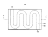
図1Aは、本発明の実施の形態1に係る流路付きプレートの構造を示す上面図である。また、図1Bは、図1AのA−A断面図である。
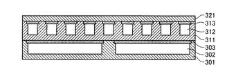
流路付きプレート100は、流体(ガス又は液体)を流通させる流路102が設けられた本体プレート101と、流路102を覆う蓋プレート103と、該蓋プレート103を覆う堆積層104とを備えている。本体プレート101には、蓋プレート103を流路102の上方に支持する支持部107が設けられている。また、流路102の端部は、流路102に流体を導入する流体導入口105、及び、流路102から流体を導出する流体導出口106となっている。
(Embodiment 1)
FIG. 1A is a top view showing the structure of the plate with flow passage according to the first embodiment of the present invention. Moreover, FIG. 1B is AA sectional drawing of FIG. 1A.
The
このような流路付きプレート100は、例えば、流路102に冷却用又は加熱用の熱媒体を流通させることにより、温度調節プレートとして用いられる。なお、この場合、本体プレート101側の主面と堆積層104側の主面とのいずれを温度調節対象である物体(例えば、基板等)の載置面としても良い。
Such a
本体プレート101及び蓋プレート103は、バルク材の金属又は合金によって形成されている。具体的には、アルミニウム(Al)、アルミニウム系合金、チタン(Ti)、チタン系合金、ステンレス鋼、銅(Cu)、銅系合金等の金属又は合金が用いられる。本体プレート101及び蓋プレート103の材料は、例えば流路102に流通させる流体の種類や用途に応じて選択される。具体的には、流路付きプレートを温度調節プレートに適用し、熱媒体として水や海水を流通させる場合には、本体プレート101の腐食を避けるために、チタン、チタン合金、ステンレス鋼等を用いると良い。また、有機溶剤等の非腐食性の流体を流通させる場合には、熱伝導性に優れたアルミニウムやアルミニウム合金を用いると良い。さらに、本体プレート101及び蓋プレート103は、同じ種類の金属又は合金によって形成されても良いし、互いに異なる金属又は合金によって形成されても良い。例えば、本体プレート101を熱伝導性に優れたアルミニウム又はアルミニウム合金によって形成し、蓋プレート103を、アルミニウム又はアルミニウム合金よりも高い強度を有するチタン又はチタン合金によって形成するといった組み合わせを用いても良い。
The
堆積層104は、金属又は合金の粉体をガスと共に加速し、成膜対象に向けて固相状態のままで吹き付けるコールドスプレー法により、蓋プレート103及び本体プレート101の蓋プレート配置面108上に形成されている。堆積層104の材料としては、上記本体プレート101及び蓋プレート103と同様に、アルミニウム(Al)、アルミニウム系合金、チタン(Ti)、チタン系合金、ステンレス鋼、銅(Cu)、銅系合金等の金属又は合金が用いられる。また、堆積層104の材料として、本体プレート101や蓋プレート103と同じ種類の金属又は合金を用いても良いし、異なる種類の金属又は合金を用いても良い。例えば、流路102を流通させる熱媒体による腐食を防止するため、本体プレート101及び蓋プレート103をステンレス鋼によって形成し、堆積層104側の熱伝導性を改善するため、堆積層104をアルミニウム合金によって形成するといった材料の選択も可能である。
The
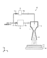
図2は、コールドスプレー法による成膜装置の構成を示す模式図である。成膜装置10は、ガス供給源からヘリウム(He)や窒素(N2)等の不活性ガスや空気等のガス(作動ガス)を導入するガス導入管11と、原料であるアルミニウム系金属の粉体1を供給する粉体供給部12と、ガス導入管11から導入されたガスを所望の温度まで加熱するヒータ13と、粉体1とガスとを混合して噴射するチャンバ14と、粉体1を噴射するノズル15と、成膜対象である基板2等を保持するホルダ16とを備えている。
FIG. 2 is a schematic diagram showing a configuration of a film forming apparatus using a cold spray method. The
粉体供給部12には、金属又は合金の微小な(例えば、粒径が10μm〜100μm程度)の粉体1が配置されている。この粉体1は、ガス導入管11に設けられたバルブ11aを操作して所望の流量のガスを粉体供給部12に導入することにより、ガスと共に粉体供給管12aを通ってチャンバ14内に供給される。
In the
ヒータ13は、導入されたガスを、例えば、50℃〜700℃程度まで加熱する。この加熱温度の上限は、粉体1を固相状態のままで基板2に吹き付けるため、原料の融点未満とする。より好ましくは、上限温度を、摂氏で融点の約60%以下に留める。これは、加熱温度が高くなるほど、粉体1が酸化する可能性が高くなるからである。従って、例えば、アルミニウム(融点:約660℃)の膜を形成する場合には、加熱温度を約660℃未満とすれば良く、約396℃以下とすればより好ましい。
The
ヒータ13において加熱されたガスは、ガス用配管13aを介してチャンバ14に導入される。なお、チャンバ14に導入されるガスの流量は、ガス導入管11に設けられているバルブ11bを操作することにより調節される。
The gas heated in the
チャンバ14の内部には、ガス用配管13aから導入されたガスにより、ノズル15から基板2に向けたガスの流れが形成されている。このチャンバ14に粉体供給部12から粉体1を供給すると、粉体1は、ガスの流れに乗って加速されると共に加熱され、ノズル15から基板2に向けて吹き付けられる。このときの衝撃により粉体1が基板2の表面に食い込み、粉体1が有している運動エネルギー及び熱エネルギーによって粉体1が塑性変形して基板2の表面に付着し、金属又は合金の堆積層3が形成される。
Inside the
粉体1を加速する速さ、即ち、ノズル15から噴射される際のガスの流速は、超音速(約340m/s以上)であり、例えば、約400m/s以上とすることが好ましい。この速さは、バルブ11bを操作してチャンバ14に導入されるガスの流量を調節することにより制御することができる。また、成膜装置10のように、基端から先端に向けて口径がテーパ状に広がっていくノズル15を使用することにより、チャンバ14内で形成されたガスの流れをノズル15の導入路で一旦絞って加速することができる。
The speed at which the
図2に示すように、ノズル15の口径に対して成膜範囲(基板2の面積)が広い場合には、ノズル15をX−Y方向に移動させながら成膜を行う。或いは、ノズル15の位置を固定し、ホルダ16側を移動させても良い。
As shown in FIG. 2, when the film formation range (the area of the substrate 2) is wide with respect to the diameter of the
次に、流路付きプレート100の製造方法について説明する。図3は、流路付きプレート100の製造方法を説明する図である。本実施の形態1においては、ステンレス鋼とアルミニウムとによって形成された流路付きプレートを製造する。
Next, the manufacturing method of the
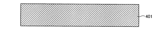
まず、図3Aに示すように、ステンレス鋼を所望の形状に成形して、本体プレート101を作製する。
次いで、図3Bに示すように、本体プレート101の一方の主面(蓋プレート配置面108)に、切削加工等により流路102となる溝109を形成すると共に、該溝109の開口縁部を切り欠くことにより支持部107を形成する。この支持部107の幅Wは、蓋プレート103を支持できる程度、即ち、溝109の幅WGRより若干広い程度であれば良い。また、支持部107の深さDは、蓋プレート103と同程度であれば良い。なお、流路102の断面形状は長方形に限定されず、任意の形状(例えば、角が丸い長方形や、台形や、三角形や、半円形や、半楕円形等)に形成しても良い。
First, as shown in FIG. 3A, stainless steel is formed into a desired shape, and the
Next, as shown in FIG. 3B, a
次いで、図3Cに示すように、予めステンレス鋼によって所定の形状に成形された蓋プレート103を支持部107に配置する。蓋プレート103の溝109を覆う面は、溝109の開口と略等しい形状(例えば、相似形)を有し、溝109の開口よりも大きな面積となるように成形されている。即ち、蓋プレートの幅WPLATEは、WGR<WPLATE≦Wであれば良い。また、蓋プレート103の厚さDPLATEは、次の工程で粉体を吹き付けられることを考慮して、材料の硬度や断面形状に応じた厚さとすることが好ましい。
Next, as shown in FIG. 3C, a
その後、これらの本体プレート101及び蓋プレート103を、成膜装置10のホルダ16にセットすると共に、アルミニウムの粉体を粉体供給部12に投入し、蓋プレート103を覆うように成膜を行う。それにより、図3のDに示す堆積層104を形成する。それにより、流路付きプレート100が完成する。なお、この後で、堆積層104の上面や側面に対して研磨や切削加工等を施すことにより、表面を平滑化すると共に、堆積層104の厚さ調整や不要な部分に付着した膜等の除去をさらに行っても良い。
Thereafter, the
以上説明した実施の形態1によれば、蓋プレート103を覆って流路102を密閉する堆積層104をコールドスプレー法により形成するので、溶接やロウ付によりバルク材を接合する従来の方法に比較して、製造時間を短縮することができる。また、溶接と異なり、母材(本体プレート、蓋プレート、堆積層)に高温の熱が加わることはないので、母材の熱歪みに起因する流路のリークを抑制することができる。さらに、母材以外の第3の部材(ロウ材や接着剤等)を使用しないので、それらの部材の流れ込みに起因する流路の汚染を抑制することができる。
According to the first embodiment described above, the
また、実施の形態1においては、コールドスプレー法により堆積層104を形成するので、本体プレート101又は蓋プレート103と堆積層104との間や、本体プレート101と蓋プレート103との間において、高い密閉性を維持することができる。これは、本体プレート101及び蓋プレート103と堆積層104とを同種金属によって形成する場合は勿論、互いに異種の金属によって形成する場合にも言える。その理由は、コールドスプレー法においては、金属の粉体1が下層(本体プレート101や蓋プレート103の上面や、それまでに堆積した堆積層104)の表面に高速に衝突して食い込み、自身を変形させて下層に強く密着するからである。このことは、本体プレート101や蓋プレート103と堆積層104との界面において、堆積層104が相手側に食い込む現象(アンカー効果と呼ばれる)が観察されることからもわかる。また、本体プレート101と蓋プレート103との間にガタが生じていても、コールドスプレー法により隙間に粉体1が充填されるので、やはり密閉性が確保される。
In the first embodiment, since the
流路付きプレート100においては、上述したように堆積層104が下層に密着しているので、堆積層104と本体プレート101や蓋プレート103との界面における伝熱性が低下することはほとんどない。また、堆積層104自体も非常に緻密な層となっているため(例えば、密度はバルク材に比較して95%以上)、堆積層104の内部においても、バルク材の90%以上という良好な伝熱性が維持されている。従って、流路付きプレート100を、例えば温度調節プレートとして用いる場合には、流路付きプレート100上に載置される物体(基板等)を効率良く、且つ均一に温度調節することができる。さらに、流路102からの流体のリークが防止されるため、流体の温度制御(即ち、載置面の温度制御)の確実性を維持することができる。
In the plate with
なお、実施の形態1においては、流体導入口105及び流体導出口106を、本体プレート101の側面に設けたが、これらを本体プレート101の下面又は堆積層104の上面に設けても良い。この場合には、流路102となる溝109を形成する際に、溝109を本体プレート101の側面よりも内側に形成して、本体プレート101の側面に開口させないようにする。そして、本体プレート101の下面側又は堆積層104の上面側から流路102に連通する孔を形成すれば良い。
In the first embodiment, the
次に、実施の形態1に係る流路付きプレート100の変形例1〜4について説明する。
図4は、変形例1を示す断面図である。図4に示す流路付きプレート110においては、蓋プレート103を支持する支持部12の深さD1を、蓋プレート103の厚さよりも大きくしている。この場合には、流路111を本体プレート101のより深部に設けることができる。
Next,
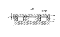
FIG. 4 is a cross-sectional view showing a first modification. In the plate with
図5は、変形例2を示す断面図である。図5に示す流路付きプレート120においては、蓋プレート103を支持する支持部22の深さD2を、蓋プレート103の厚さよりも小さくしている。この場合には、流路121及び支持部122を形成する切削工程の時間を短縮しつつ、堆積層104の形成工程において、蓋プレート103の位置ずれを防止することができる。
FIG. 5 is a cross-sectional view showing a second modification. In the plate with
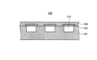
図6は、変形例3を示す断面図である。図6に示す流路付きプレート130においては、本体プレート101の上面に蓋プレート103を載置している。この場合には、蓋プレート103を支持する支持部を形成する切削工程を削減することができる。また、蓋プレート103を支持部の内側に収める必要がなくなるため、蓋プレート103の形状に対する制約を緩和することができる。
FIG. 6 is a cross-sectional view showing a third modification. In the plate with
図7は、変形例4を示す断面図である。図7に示す流路付きプレート140においては、隣接する流路131の間で連続するように形成された蓋プレート141を、本体プレート101の上面に配置している。この場合は、蓋プレート103を、少なくとも流路131を覆うことができる形状に成形すれば良いため、蓋プレート103の形成工程を簡素化することができる。
FIG. 7 is a cross-sectional view showing a fourth modification. In the plate with
(実施の形態2)
次に、本発明の実施の形態2に係る流路付きプレートについて説明する。本実施の形態2においては、流路付きプレートを、CVD法(化学気相成長法)による成膜装置等において、成膜チャンバ内に備えられて基板を冷却するコールドプレートとして用いる。図8Aは、実施の形態2に係る流路付きプレートであるコールドプレートを示す上面図である。また、図8Bは、図8Aに示すコールドプレートを示す一部断面側面図である。
(Embodiment 2)
Next, the plate with flow paths according to the second embodiment of the present invention will be described. In the second embodiment, the plate with a flow path is used as a cold plate that is provided in a film forming chamber and cools the substrate in a film forming apparatus or the like by a CVD method (chemical vapor deposition method). FIG. 8A is a top view showing a cold plate that is a plate with flow passages according to the second embodiment. 8B is a partial cross-sectional side view showing the cold plate shown in FIG. 8A.
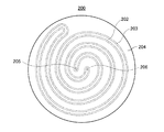
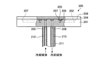
コールドプレート200は、流路202及び支持部207が設けられた本体プレート201と、支持部207に保持され、流路202を覆う蓋プレート203と、蓋プレート203を覆う堆積層204とを備えている。本体プレート201及び蓋プレート203は、実施の形態1と同様に、例えばアルミニウムのバルク材によって形成されている。一方、堆積層204は、例えばアルミニウム粉体を用いたコールドスプレー法によって形成されている。この堆積層204の上面が、冷却対象である基板を載置する載置面となっている。
The
流路202は、中心から外周に向けて広がってから再度中心に戻る渦巻き状をなしており、流路202の両端は中心付近に位置している。本体プレート201の中心付近には、流路202内に冷却媒体を導入する熱媒体導入路205と、流路202内から冷却媒体を導出する熱媒体導出路206とが設けられている。
The
このようなコールドプレート200は、シャフト211に支持されて用いられる。シャフト211の内側には、熱媒体導入路205に接続される冷却媒体供給管212と、熱媒体導出路206に接続される冷却媒体排出管213とが収納されている。
Such a
コールドプレート200の製造方法は、次のとおりである。即ち、図3を参照しながら実施の形態1において説明したものと同様に、まず、本体プレート201の一方の主面(蓋プレート配置面208)に流路202となる溝209を形成すると共に、該溝209の開口縁部を切り欠くことにより支持部207を形成する。そして、溝209の開口と略等しい形状(例えば、相似形)を有し、該開口より大きい面積を有する蓋プレート203を、支持部207に配置する。続いて、図2に示す成膜装置10により、蓋プレート203を覆う堆積層204を形成する。さらに、本体プレート201の下面側から、熱媒体導入路205及び熱媒体導出路206を形成する。
The manufacturing method of the
実施の形態2によれば、図8Aに示すような複雑な流路パターンを有し、且つ良好な伝熱性と流路の密閉性とを有する温度調節装置を容易に作製することが可能である。
なお、本実施の形態2においては、堆積層204側の表面を基板の載置面とするため、熱媒体導入路205及び熱媒体導出路206を本体プレート201側に設けたが、反対に、本体プレート201側の表面を基板の載置面とし、熱媒体導入路205及び熱媒体導出路206を堆積層204側に設けても良い。
According to the second embodiment, it is possible to easily produce a temperature control device having a complicated flow path pattern as shown in FIG. 8A and having good heat transfer properties and flow path sealing properties. .
In the second embodiment, the heat
(実施の形態3)
次に、本発明の実施の形態3に係る流路付きプレートについて説明する。本実施の形態3においては、流路付きプレートを、CVD法による成膜装置等において、成膜チャンバ内に備えられて2種類の成膜ガスを基板に供給するシャワープレートに適用する。図9Aは、実施の形態3に係る流路付きプレートであるシャワープレートを示す上面図である。また、図9Bは、図9AのB−B断面図である。
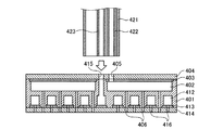
(Embodiment 3)
Next, the plate with flow passage according to the third embodiment of the present invention will be described. In
図9A及び図9Bに示すように、シャワープレート300は、第1の成膜ガスを流通させる第1流路302が形成された本体プレート301と、第1流路302を覆う蓋プレート303と、該蓋プレート303を覆うと共に、第2の成膜ガスを流通させる第2流路312が形成された堆積層311と、第2流路312を覆う蓋プレート313と、該蓋プレート313を覆う堆積層321とを備えている。このようなシャワープレート300は、シャフト331によって支持されて用いられる。シャフト331の内側には、第1の成膜ガスを供給する第1ガス供給管332と、第2の成膜ガスを供給する第2ガス供給管333とが収納されている。
As shown in FIGS. 9A and 9B, the
シャワープレート300には、第1ガス供給菅332に接続されて第1の成膜ガスを第1流路302に導入する第1ガス導入路304と、第2ガス供給菅333に接続されて第2の成膜ガスを第2流路312に導入する第2ガス導入路314とが設けられている。また、シャワープレート300には、第1流路302を流通する第1の成膜ガスを導出する複数の第1ガス導出孔305と、第2流路312を流通する第2の成膜ガスを導出する複数の第2ガス導出孔315とが設けられている。
The
また、第1流路302と第2流路312とは、第1ガス導出孔305が第2流路312に接触したり、第2ガス導入路314が第1流路302に接触したりしないように、互いに位置をずらして配置されている。
Further, the
シャワープレート300を使用する際には、第1ガス供給管332から供給された第1の成膜ガスが、第1流路302を介して第1ガス導出孔305から放出され、第2ガス供給管333から供給された第2の成膜ガスが、第2流路312を介して第2ガス導出孔315から放出される。これらの第1及び第2の成膜ガスは、シャワープレート300から放出された後で混合され、成膜に寄与することになる。
When the
次に、シャワープレート300の製造方法について説明する。図10A〜図10Iは、シャワープレート300の製造方法を説明する図である。実施の形態3においては、シャワープレート300の材料としてアルミニウム合金を用いる。
Next, a method for manufacturing the
まず、図10Aに示すように、バルクのアルミニウム合金を所望の形状に成形して、本体プレート301を作製する。
次いで、図10Bに示すように、切削加工等により、本体プレート301の一方の主面に第1流路302となる溝306を形成すると共に、該溝306の開口縁部を切り欠くことにより支持部307を形成する。そして、図10Cに示すように、溝306の開口と略等しい形状(例えば、相似形)であり、該開口より大きな面積を有するアルミニウム合金の蓋プレート303を、支持部307に配置する。
First, as shown in FIG. 10A, a bulk aluminum alloy is formed into a desired shape to produce a
Next, as shown in FIG. 10B, a
これらの本体プレート301及び蓋プレート303を、図2に示す成膜装置10のホルダ16にセットすると共に、アルミニウム合金の粉体を粉体供給部12に投入して、コールドスプレー法により本体プレート301及び蓋プレート303を覆うように成膜を行う。それにより、図10Dに示す堆積層311が形成される。堆積層311の厚さは、この後の工程で第2流路312を形成できる程度に十分な厚さとし、好ましくは、本体プレート301と同程度にすると良い。また、成膜後、研磨等により堆積層311の表面を平滑にすると共に、不要な部分に付着した膜を除去しておく。
The
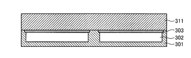
次いで、図10Eに示すように、切削加工等により、堆積層311に第2流路312となる溝316を形成すると共に、該溝316の開口縁部を切り欠くことにより支持部317を形成する。そして、図10Fに示すように、溝316の開口と略等しい形状(例えば、相似形)であり、該開口より大きな面積を有するアルミニウム合金の蓋プレート313を、支持部317に配置する。これを成膜装置10にセットし、アルミニウム合金の粉体を用いて、コールドスプレー法により堆積層311及び蓋プレート313を覆うように成膜を行う。それにより、図10Gに示す堆積層321が形成される。さらに、研磨等により堆積層321の表面を平滑にし、不要な部分に付着した膜を除去しておく。
Next, as shown in FIG. 10E, a
続いて、図10Hに示すように、本体プレート301の表面側から、本体プレート301を貫通して第1流路302に連通する第1ガス導入路304を設ける。同様に、本体プレート301及び堆積層311を貫通して第2流路312に連通する第2ガス導入路314を形成する。また、堆積層321の表面側から、堆積層321、堆積層311、及び蓋プレート303を貫通して第1流路302に連通する複数の第1ガス導出孔305を形成する。同様に、堆積層321及び蓋プレート313を貫通して第2流路312に連通する複数の第2ガス導出孔315を形成する。そして、図10Iに示すように、第1ガス供給管332を第1ガス導入路304に接続し、第2ガス供給管333を第2ガス導入路314に接続する。さらに、シャフト331を本体プレート301に電子ビーム溶接等により接合することにより、図9A及び図9Bに示すシャワープレート300が完成する。
Subsequently, as illustrated in FIG. 10H, a first
以上説明した実施の形態3によれば、第1流路302及び第2流路312上にそれぞれ配置された蓋プレート303及び313の周囲を、コールドスプレー法によって形成された堆積層311及び321によってそれぞれ覆うので、第1流路302及び第2流路312の各々の密閉性を確保することができる。従って、第1ガス供給管332及び第2ガス供給管333の2系統からそれぞれ供給される2種類の成膜ガスがシャワープレート内で混合したり、シャワープレート外にリークするといった事態を防ぐことができる。
According to the third embodiment described above, the surroundings of the
なお、実施の形態3においては、本体プレート301側に第1ガス導入路304及び第2ガス導入路314を設け、堆積層321側に第1ガス導出孔305及び第2ガス導出孔315を設けたが、反対に、堆積層321側に第1ガス導入路304及び第2ガス導入路314を設け、本体プレート301側に第1ガス導出孔305及び第2ガス導出孔315を設けることとしても良い。
In the third embodiment, the first
また、実施の形態3においては、支持部307、317の深さを、蓋プレート303、313の厚さとそれぞれ同程度としている。しかしながら、実施の形態1の変形例1や変形例2(図4及び図5参照)と同様に、支持部307、317の深さを、蓋プレート303、313の厚さよりも大きくしても良いし、小さくしても良い。或いは、変形例3と同様に(図6参照)、支持部307、317を設けずに、流路302、312より若干大きく成形された蓋プレート303、313を本体プレート301上又は堆積層311上にそれぞれ載置して、第1流路302や第2流路312を覆うようにしても良い。
In the third embodiment, the depths of the
さらに、実施の形態3においては、2つの流路(第1及び第2流路)を有するシャワープレートを作製したが、図10E〜図10Gに示す工程を繰り返すことにより、流路の数を3つ以上としても良いし、これらの工程を省略することにより、流路の数1つのみとしても良い。
Furthermore, in
(実施の形態4)
次に、本発明の実施の形態4に係る流路付きプレートについて説明する。本実施の形態4においては、流路付きプレートを、実施の形態3と同様に、2種類のガスを成膜チャンバ内の基板に供給するシャワープレートに適用する。図11は、実施の形態4に係る流路付きプレートであるシャワープレートを示す断面図である。なお、該シャワープレートの上面図は、図9Aに示すものと同様である。
(Embodiment 4)
Next, the plate with flow passage according to the fourth embodiment of the present invention will be described. In the fourth embodiment, the plate with a flow path is applied to a shower plate that supplies two types of gases to the substrate in the film formation chamber, as in the third embodiment. FIG. 11 is a cross-sectional view showing a shower plate that is a plate with flow passages according to the fourth embodiment. The top view of the shower plate is the same as that shown in FIG. 9A.
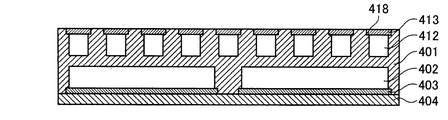
図11に示すように、シャワープレート400は、第1の成膜ガスを流通させる第1流路402と、第2の成膜ガスを流通させる第2流路412とが形成された本体プレート401と、第1流路402を覆う蓋プレート403と、該蓋プレート403を覆う堆積層404と、第2流路412を覆う蓋プレート413と、該蓋プレート413を覆う堆積層414とを備えている。このようなシャワープレート400は、シャフト421によって支持されて用いられる。シャフト421の内側には、第1の成膜ガスを供給する第1ガス供給管422と、第2の成膜ガスを供給する第2ガス供給管423とが収納されている。
As shown in FIG. 11, the
シャワープレート400には、第1ガス供給菅422に接続されて第1の成膜ガスを第1流路402に導入する第1ガス導入路405と、第2ガス導入管423に接続されて第2の成膜ガスを第2流路412に導入する第2ガス導入路415とが設けられている。また、シャワープレート400には、第1流路402を流通する第1の成膜ガスを導出する複数の第1ガス導出孔406と、第2流路412を流通する第2の成膜ガスを導出する複数の第2ガス導出孔416とが設けられている。
The
次に、シャワープレート400の製造方法について説明する。図12A〜図12Hは、シャワープレート400の製造方法を説明する図である。実施の形態4においては、シャワープレート400の材料としてアルミニウム合金を用いる。
Next, a method for manufacturing the
まず、図12Aに示すように、バルクのアルミニウム合金を所望の形状に成形して、本体プレート401を作製する。
次いで、図12Bに示すように、本体プレート401の一方の主面に、第1流路402となる溝407を形成すると共に、該溝407の開口縁部を切り欠くことにより支持部408を形成する。また、本体プレート401の他方の主面に、第2流路412となる溝417を形成すると共に、該溝417の開口縁部を切り欠くことにより支持部418を形成する。
First, as shown in FIG. 12A, a bulk aluminum alloy is formed into a desired shape to produce a
Next, as shown in FIG. 12B, a
図12Cに示すように、溝407の開口と略等しい形状(例えば、相似形)であり、該開口より大きい面積を有するアルミニウム合金の蓋プレート403を支持部408に配置する。これを成膜装置10のホルダ16にセットすると共に、アルミニウム合金の粉体を粉体供給部12に投入して、コールドスプレー法により本体プレート401及び蓋プレート403を覆うように成膜を行う。それにより、図12Dに示す堆積層404が形成される。
As shown in FIG. 12C, an aluminum
次いで、図12Eに示すように、本体プレート401の天地を逆転し、溝417と略等しい形状(例えば、相似形)であり、該開口より大きい面積を有するアルミニウム合金の蓋プレート413を支持部418に配置する。これを成膜装置10のホルダ16にセットし、コールドスプレー法により本体プレート401及び蓋プレート413を覆うように成膜を行う。それにより、図12Fに示す堆積層414が形成される。
Next, as shown in FIG. 12E, the top and bottom of the
続いて、図12Gに示すように、堆積層404の表面側から、堆積層404及び蓋プレート403を貫通して第1流路402に連通する第1ガス導入路405を形成する。同様に、堆積層404及び本体プレート401を貫通して第2流路412に連通する第2ガス導入路415を形成する。また、堆積層414の表面側から、堆積層414及び本体プレート401を貫通して第1流路402に連通する複数の第1ガス導出孔406を形成する。同様に、堆積層414及び蓋プレート413を貫通して第2流路412に連通する複数の第2ガス導出孔416を形成する。そして、図12Hに示すように、第1ガス供給管422を第1ガス導入路405に接続し、第2ガス供給管423を第2ガス導入路415に接続する。さらに、シャフト421を堆積層404に電子ビーム溶接等により接合する。それにより、図11に示すシャワープレート400が完成する。
Subsequently, as shown in FIG. 12G, a first
以上説明した実施の形態4によれば、第1流路402及び第2流路412の密閉性が確保されたシャワープレートを、容易に製造することができる。従って、このようなシャワープレート400を成膜チャンバ内で用いることにより、シャワープレート400内における2種類の成膜ガスの混合や、これらの成膜ガスのシャワープレート外へのリークを防止することができる。
According to the fourth embodiment described above, a shower plate in which the
なお、実施の形態4においては、第1ガス導入路405及び第2ガス導入路415を堆積層404側に設け、第1ガス導出孔406及び第2ガス導出孔416を堆積層414側に設けたが、その逆であっても構わない。また、支持部408及び418の深さについても、蓋プレート403及び413の厚さより大きくしても良いし、小さくしても良いし、或いは支持部408及び418を設けないこととしても良い。
In the fourth embodiment, the first
本発明は、流路付きプレート及びその製造方法において利用可能であり、より具体的には、半導体や液晶表示装置や光ディスク等の製造プロセスにおいて、基板等の温度調整に用いられる温度調節プレート又はコールドプレートや、成膜ガス等の供給に用いられるシャワープレートにおいて利用可能である。 INDUSTRIAL APPLICABILITY The present invention can be used in a plate with a flow path and a method for manufacturing the plate, and more specifically, in a manufacturing process of a semiconductor, a liquid crystal display device, an optical disk, etc. It can be used in a plate or a shower plate used for supplying a film forming gas or the like.
1 粉体
2 基板
3 堆積層
10 成膜装置
11 ガス導入管
11a、11b バルブ
12a 粉体供給管
12 粉体供給部
13a ガス用配管
13 ヒータ
14 チャンバ
15 ノズル
16 ホルダ
100 プレート
102、111、121、131、202 流路
103、141、203、303、313、403、413 蓋プレート
104、204、311、321、404、414 堆積層
105 流体導入口
106 流体導出口
108、208 蓋プレート配置面
109、306、316、407、417 溝
200 コールドプレート
201、301、401 本体プレート
205 熱媒体導入路
206 熱媒体導出路
107、207、307、317、408、418 支持部
211、331、421 シャフト
213 冷却媒体排出管
212 冷却媒体供給管
300、400 シャワープレート
302、402 第1流路
304、405 第1ガス導入路
305、406 第1ガス導出孔
312、412 第2流路
314、415 第2ガス導入路
315、416 第2ガス導出孔
332、422 第1ガス供給管
333、423 第2ガス供給管
DESCRIPTION OF
Claims (13)
金属又は合金によって形成された本体プレートに、前記流路となる溝を形成する流路形成工程と、
前記溝を覆う蓋プレートを、前記溝の上部に配置する蓋配置工程と、
金属又は合金の粉体をガスと共に加速し、前記本体プレート及び前記蓋プレートに向けて固相状態のままで吹き付けることにより、前記蓋プレートを覆う堆積層を形成する堆積層形成工程と、
を含むことを特徴とする流路付きプレートの製造方法。 In the manufacturing method of the plate with a flow path in which the flow path for circulating the fluid is formed inside the plate,
A flow path forming step of forming a groove to be the flow path in a body plate formed of a metal or an alloy;
A lid placement step of placing a lid plate covering the groove on top of the groove;
A deposition layer forming step of forming a deposition layer covering the lid plate by accelerating the powder of the metal or alloy together with the gas and spraying the powder in the solid phase toward the main body plate and the lid plate;
The manufacturing method of the plate with a flow path characterized by including these.
金属又は合金によって形成され、流路となる溝が設けられた本体プレートと、
前記溝を覆う蓋プレートと、
金属又は合金の粉体をガスと共に加速し、前記本体プレート及び前記蓋プレートに向けて固相状態のままで吹き付けることにより形成され、前記蓋プレートを覆う堆積層と、
を備えることを特徴とする流路付きプレート。 In the plate with a flow path in which the flow path for circulating the fluid is formed inside the plate,
A body plate formed of a metal or an alloy and provided with a groove serving as a flow path;
A lid plate covering the groove;
A deposition layer covering the lid plate, formed by accelerating the powder of the metal or alloy together with the gas and spraying it in the solid state toward the body plate and the lid plate;
A plate with a flow path, comprising:
前記第2の溝を覆う第2の蓋プレートと、
金属又は合金の粉体をガスと共に加速し、前記堆積層及び前記第2の蓋プレートに向けて固相状態のままで吹き付けることにより形成され、前記第2の蓋プレートを覆う第2の堆積層と、
をさらに備えることを特徴とする請求項5〜8のいずれか1項に記載の流路付きプレート。 A second groove serving as a second flow path is formed in the deposited layer;
A second lid plate covering the second groove;
Second deposition layer formed by accelerating powder of metal or alloy together with gas and spraying the deposition layer and the second lid plate in a solid phase state, and covering the second lid plate When,
The plate with flow paths according to any one of claims 5 to 8, further comprising:
前記流路付きプレートに、前記流路に連通して該流路に熱媒体を導入する熱媒体導入路と、前記流路に連通して該流路から熱媒体を導出する熱媒体導出路とが設けられていることを特徴とする温度調節プレート。 A plate with a flow path according to any one of claims 5 to 8,
A heat medium introduction path that communicates with the flow path and introduces a heat medium into the flow path, and a heat medium lead-out path that communicates with the flow path and derives the heat medium from the flow path; Is provided with a temperature control plate.
前記流路付きプレートに、前記流路に連通して該流路に冷却媒体を導入する熱媒体導入路と、前記流路に連通して該流路から冷却媒体を導出する熱媒体導出路とが設けられていることを特徴とするコールドプレート。 A plate with a flow path according to any one of claims 5 to 8,
A heat medium introduction path that communicates with the flow path and introduces a cooling medium into the flow path, and a heat medium lead-out path that communicates with the flow path and derives the cooling medium from the flow path; A cold plate characterized by that.
前記流路付きプレートに、前記流路に連通して該流路に所定の成分を有するガスを導入するガス導入路と、前記流路に連通して該流路から前記ガスを導出するガス導出孔とが設けられていることを特徴とするシャワープレート。 The plate with a flow path according to any one of claims 5 to 10,
A gas introduction path that communicates with the flow path and introduces a gas having a predetermined component into the flow path, and a gas outlet that communicates with the flow path and derives the gas from the flow path. A shower plate having holes.
Priority Applications (6)
| Application Number | Priority Date | Filing Date | Title |
|---|---|---|---|
| JP2010157235A JP5463224B2 (en) | 2010-07-09 | 2010-07-09 | Manufacturing method of plate with flow path, plate with flow path, temperature control plate, cold plate, and shower plate |
| KR1020137000378A KR101409953B1 (en) | 2010-07-09 | 2011-07-06 | Method of manufacturing plate with passage, plate with passage, temperature adjustment plate, cold plate, and shower plate |
| PCT/JP2011/065507 WO2012005305A1 (en) | 2010-07-09 | 2011-07-06 | Manufacturing method for channel plate, channel plate, temperature adjustment plate, cold plate, and shower plate |
| EP11803639.1A EP2592647B1 (en) | 2010-07-09 | 2011-07-06 | Manufacturing method for plate |
| US13/808,783 US10279441B2 (en) | 2010-07-09 | 2011-07-06 | Method of manufacturing plate with passage, plate with passage, temperature adjustment plate, cold plate, and shower plate |
| CN201180030775.8A CN102959696B (en) | 2010-07-09 | 2011-07-06 | Manufacture method with stream plate, band stream plate, temperature adjusting plate, cold drawing and bath board |
Applications Claiming Priority (1)
| Application Number | Priority Date | Filing Date | Title |
|---|---|---|---|
| JP2010157235A JP5463224B2 (en) | 2010-07-09 | 2010-07-09 | Manufacturing method of plate with flow path, plate with flow path, temperature control plate, cold plate, and shower plate |
Publications (2)
| Publication Number | Publication Date |
|---|---|
| JP2012019164A true JP2012019164A (en) | 2012-01-26 |
| JP5463224B2 JP5463224B2 (en) | 2014-04-09 |
Family
ID=45441281
Family Applications (1)
| Application Number | Title | Priority Date | Filing Date |
|---|---|---|---|
| JP2010157235A Active JP5463224B2 (en) | 2010-07-09 | 2010-07-09 | Manufacturing method of plate with flow path, plate with flow path, temperature control plate, cold plate, and shower plate |
Country Status (6)
| Country | Link |
|---|---|
| US (1) | US10279441B2 (en) |
| EP (1) | EP2592647B1 (en) |
| JP (1) | JP5463224B2 (en) |
| KR (1) | KR101409953B1 (en) |
| CN (1) | CN102959696B (en) |
| WO (1) | WO2012005305A1 (en) |
Cited By (98)
| Publication number | Priority date | Publication date | Assignee | Title |
|---|---|---|---|---|
| JP2010209389A (en) * | 2009-03-09 | 2010-09-24 | Kanto Auto Works Ltd | Method for manufacturing electrocast shell having temperature-controlling tube |
| JP2013169038A (en) * | 2012-02-14 | 2013-08-29 | Fanuc Ltd | Rotor with cage conductor in which reinforcement structure is formed and manufacturing method therefor |
| JP2014192372A (en) * | 2013-03-27 | 2014-10-06 | Tokyo Electron Ltd | Microwave heating apparatus |
| KR20150038154A (en) * | 2012-07-18 | 2015-04-08 | 어플라이드 머티어리얼스, 인코포레이티드 | Pedestal with multi-zone temperature control and multiple purge capabilities |
| US9741593B2 (en) | 2015-08-06 | 2017-08-22 | Applied Materials, Inc. | Thermal management systems and methods for wafer processing systems |
| US9754800B2 (en) | 2010-05-27 | 2017-09-05 | Applied Materials, Inc. | Selective etch for silicon films |
| US9768034B1 (en) | 2016-11-11 | 2017-09-19 | Applied Materials, Inc. | Removal methods for high aspect ratio structures |
| US9773648B2 (en) | 2013-08-30 | 2017-09-26 | Applied Materials, Inc. | Dual discharge modes operation for remote plasma |
| US9773695B2 (en) | 2014-07-31 | 2017-09-26 | Applied Materials, Inc. | Integrated bit-line airgap formation and gate stack post clean |
| US9837284B2 (en) | 2014-09-25 | 2017-12-05 | Applied Materials, Inc. | Oxide etch selectivity enhancement |
| US9837249B2 (en) | 2014-03-20 | 2017-12-05 | Applied Materials, Inc. | Radial waveguide systems and methods for post-match control of microwaves |
| US9842744B2 (en) | 2011-03-14 | 2017-12-12 | Applied Materials, Inc. | Methods for etch of SiN films |
| US9865484B1 (en) | 2016-06-29 | 2018-01-09 | Applied Materials, Inc. | Selective etch using material modification and RF pulsing |
| US9881805B2 (en) | 2015-03-02 | 2018-01-30 | Applied Materials, Inc. | Silicon selective removal |
| US9885117B2 (en) | 2014-03-31 | 2018-02-06 | Applied Materials, Inc. | Conditioned semiconductor system parts |
| US9934942B1 (en) | 2016-10-04 | 2018-04-03 | Applied Materials, Inc. | Chamber with flow-through source |
| US9947549B1 (en) | 2016-10-10 | 2018-04-17 | Applied Materials, Inc. | Cobalt-containing material removal |
| US9966240B2 (en) | 2014-10-14 | 2018-05-08 | Applied Materials, Inc. | Systems and methods for internal surface conditioning assessment in plasma processing equipment |
| US9978564B2 (en) | 2012-09-21 | 2018-05-22 | Applied Materials, Inc. | Chemical control features in wafer process equipment |
| KR101876548B1 (en) * | 2016-12-30 | 2018-07-09 | 상구정공(주) | Plate of showerhead and Method of manufacturing the same |
| US10026621B2 (en) | 2016-11-14 | 2018-07-17 | Applied Materials, Inc. | SiN spacer profile patterning |
| US10032606B2 (en) | 2012-08-02 | 2018-07-24 | Applied Materials, Inc. | Semiconductor processing with DC assisted RF power for improved control |
| US10043674B1 (en) | 2017-08-04 | 2018-08-07 | Applied Materials, Inc. | Germanium etching systems and methods |
| US10043684B1 (en) | 2017-02-06 | 2018-08-07 | Applied Materials, Inc. | Self-limiting atomic thermal etching systems and methods |
| US10049891B1 (en) | 2017-05-31 | 2018-08-14 | Applied Materials, Inc. | Selective in situ cobalt residue removal |
| US10062585B2 (en) | 2016-10-04 | 2018-08-28 | Applied Materials, Inc. | Oxygen compatible plasma source |
| US10062578B2 (en) | 2011-03-14 | 2018-08-28 | Applied Materials, Inc. | Methods for etch of metal and metal-oxide films |
| US10062579B2 (en) | 2016-10-07 | 2018-08-28 | Applied Materials, Inc. | Selective SiN lateral recess |
| US10062575B2 (en) | 2016-09-09 | 2018-08-28 | Applied Materials, Inc. | Poly directional etch by oxidation |
| US10128086B1 (en) | 2017-10-24 | 2018-11-13 | Applied Materials, Inc. | Silicon pretreatment for nitride removal |
| US10147620B2 (en) | 2015-08-06 | 2018-12-04 | Applied Materials, Inc. | Bolted wafer chuck thermal management systems and methods for wafer processing systems |
| US10163696B2 (en) | 2016-11-11 | 2018-12-25 | Applied Materials, Inc. | Selective cobalt removal for bottom up gapfill |
| US10170336B1 (en) | 2017-08-04 | 2019-01-01 | Applied Materials, Inc. | Methods for anisotropic control of selective silicon removal |
| KR20190010731A (en) * | 2013-05-07 | 2019-01-30 | 어플라이드 머티어리얼스, 인코포레이티드 | Electrostatic chuck having thermally isolated zones with minimal crosstalk |
| US10224210B2 (en) | 2014-12-09 | 2019-03-05 | Applied Materials, Inc. | Plasma processing system with direct outlet toroidal plasma source |
| US10242908B2 (en) | 2016-11-14 | 2019-03-26 | Applied Materials, Inc. | Airgap formation with damage-free copper |
| US10256079B2 (en) | 2013-02-08 | 2019-04-09 | Applied Materials, Inc. | Semiconductor processing systems having multiple plasma configurations |
| US10256112B1 (en) | 2017-12-08 | 2019-04-09 | Applied Materials, Inc. | Selective tungsten removal |
| US10283324B1 (en) | 2017-10-24 | 2019-05-07 | Applied Materials, Inc. | Oxygen treatment for nitride etching |
| US10283321B2 (en) | 2011-01-18 | 2019-05-07 | Applied Materials, Inc. | Semiconductor processing system and methods using capacitively coupled plasma |
| US10297458B2 (en) | 2017-08-07 | 2019-05-21 | Applied Materials, Inc. | Process window widening using coated parts in plasma etch processes |
| JP2019515506A (en) * | 2016-05-06 | 2019-06-06 | アプライド マテリアルズ インコーポレイテッドApplied Materials,Incorporated | Substrate support for whole area reverse flow heat exchange |
| US10319649B2 (en) | 2017-04-11 | 2019-06-11 | Applied Materials, Inc. | Optical emission spectroscopy (OES) for remote plasma monitoring |
| US10319739B2 (en) | 2017-02-08 | 2019-06-11 | Applied Materials, Inc. | Accommodating imperfectly aligned memory holes |
| US10319600B1 (en) | 2018-03-12 | 2019-06-11 | Applied Materials, Inc. | Thermal silicon etch |
| US10354889B2 (en) | 2017-07-17 | 2019-07-16 | Applied Materials, Inc. | Non-halogen etching of silicon-containing materials |
| US10403507B2 (en) | 2017-02-03 | 2019-09-03 | Applied Materials, Inc. | Shaped etch profile with oxidation |
| US10424485B2 (en) | 2013-03-01 | 2019-09-24 | Applied Materials, Inc. | Enhanced etching processes using remote plasma sources |
| US10424464B2 (en) | 2015-08-07 | 2019-09-24 | Applied Materials, Inc. | Oxide etch selectivity systems and methods |
| US10431429B2 (en) | 2017-02-03 | 2019-10-01 | Applied Materials, Inc. | Systems and methods for radial and azimuthal control of plasma uniformity |
| US10468267B2 (en) | 2017-05-31 | 2019-11-05 | Applied Materials, Inc. | Water-free etching methods |
| US10468285B2 (en) | 2015-02-03 | 2019-11-05 | Applied Materials, Inc. | High temperature chuck for plasma processing systems |
| US10465294B2 (en) | 2014-05-28 | 2019-11-05 | Applied Materials, Inc. | Oxide and metal removal |
| US10490406B2 (en) | 2018-04-10 | 2019-11-26 | Appled Materials, Inc. | Systems and methods for material breakthrough |
| US10497573B2 (en) | 2018-03-13 | 2019-12-03 | Applied Materials, Inc. | Selective atomic layer etching of semiconductor materials |
| US10504754B2 (en) | 2016-05-19 | 2019-12-10 | Applied Materials, Inc. | Systems and methods for improved semiconductor etching and component protection |
| US10504700B2 (en) | 2015-08-27 | 2019-12-10 | Applied Materials, Inc. | Plasma etching systems and methods with secondary plasma injection |
| US10522371B2 (en) | 2016-05-19 | 2019-12-31 | Applied Materials, Inc. | Systems and methods for improved semiconductor etching and component protection |
| US10541246B2 (en) | 2017-06-26 | 2020-01-21 | Applied Materials, Inc. | 3D flash memory cells which discourage cross-cell electrical tunneling |
| US10541184B2 (en) | 2017-07-11 | 2020-01-21 | Applied Materials, Inc. | Optical emission spectroscopic techniques for monitoring etching |
| US10546729B2 (en) | 2016-10-04 | 2020-01-28 | Applied Materials, Inc. | Dual-channel showerhead with improved profile |
| US10566206B2 (en) | 2016-12-27 | 2020-02-18 | Applied Materials, Inc. | Systems and methods for anisotropic material breakthrough |
| US10573527B2 (en) | 2018-04-06 | 2020-02-25 | Applied Materials, Inc. | Gas-phase selective etching systems and methods |
| US10573496B2 (en) | 2014-12-09 | 2020-02-25 | Applied Materials, Inc. | Direct outlet toroidal plasma source |
| JP2020033614A (en) * | 2018-08-30 | 2020-03-05 | 住友金属鉱山株式会社 | Film forming apparatus and film forming method |
| US10593560B2 (en) | 2018-03-01 | 2020-03-17 | Applied Materials, Inc. | Magnetic induction plasma source for semiconductor processes and equipment |
| US10593523B2 (en) | 2014-10-14 | 2020-03-17 | Applied Materials, Inc. | Systems and methods for internal surface conditioning in plasma processing equipment |
| US10615047B2 (en) | 2018-02-28 | 2020-04-07 | Applied Materials, Inc. | Systems and methods to form airgaps |
| US10629473B2 (en) | 2016-09-09 | 2020-04-21 | Applied Materials, Inc. | Footing removal for nitride spacer |
| US10672642B2 (en) | 2018-07-24 | 2020-06-02 | Applied Materials, Inc. | Systems and methods for pedestal configuration |
| US10679870B2 (en) | 2018-02-15 | 2020-06-09 | Applied Materials, Inc. | Semiconductor processing chamber multistage mixing apparatus |
| CN111293057A (en) * | 2018-12-07 | 2020-06-16 | 应用材料公司 | Component, method of manufacturing a component, and method of cleaning a component |
| US10699879B2 (en) | 2018-04-17 | 2020-06-30 | Applied Materials, Inc. | Two piece electrode assembly with gap for plasma control |
| US10727080B2 (en) | 2017-07-07 | 2020-07-28 | Applied Materials, Inc. | Tantalum-containing material removal |
| US10755941B2 (en) | 2018-07-06 | 2020-08-25 | Applied Materials, Inc. | Self-limiting selective etching systems and methods |
| US10854426B2 (en) | 2018-01-08 | 2020-12-01 | Applied Materials, Inc. | Metal recess for semiconductor structures |
| US10872778B2 (en) | 2018-07-06 | 2020-12-22 | Applied Materials, Inc. | Systems and methods utilizing solid-phase etchants |
| US10886137B2 (en) | 2018-04-30 | 2021-01-05 | Applied Materials, Inc. | Selective nitride removal |
| KR102199738B1 (en) * | 2020-04-24 | 2021-01-08 | (주)코리아스타텍 | Direct cooling type electrostatic chuck for dry etching equipment |
| US10892198B2 (en) | 2018-09-14 | 2021-01-12 | Applied Materials, Inc. | Systems and methods for improved performance in semiconductor processing |
| US10903054B2 (en) | 2017-12-19 | 2021-01-26 | Applied Materials, Inc. | Multi-zone gas distribution systems and methods |
| US10920319B2 (en) | 2019-01-11 | 2021-02-16 | Applied Materials, Inc. | Ceramic showerheads with conductive electrodes |
| US10920320B2 (en) | 2017-06-16 | 2021-02-16 | Applied Materials, Inc. | Plasma health determination in semiconductor substrate processing reactors |
| US10943834B2 (en) | 2017-03-13 | 2021-03-09 | Applied Materials, Inc. | Replacement contact process |
| US10964512B2 (en) | 2018-02-15 | 2021-03-30 | Applied Materials, Inc. | Semiconductor processing chamber multistage mixing apparatus and methods |
| US11049755B2 (en) | 2018-09-14 | 2021-06-29 | Applied Materials, Inc. | Semiconductor substrate supports with embedded RF shield |
| US11062887B2 (en) | 2018-09-17 | 2021-07-13 | Applied Materials, Inc. | High temperature RF heater pedestals |
| US11121002B2 (en) | 2018-10-24 | 2021-09-14 | Applied Materials, Inc. | Systems and methods for etching metals and metal derivatives |
| US11239061B2 (en) | 2014-11-26 | 2022-02-01 | Applied Materials, Inc. | Methods and systems to enhance process uniformity |
| US11257693B2 (en) | 2015-01-09 | 2022-02-22 | Applied Materials, Inc. | Methods and systems to improve pedestal temperature control |
| US11276590B2 (en) | 2017-05-17 | 2022-03-15 | Applied Materials, Inc. | Multi-zone semiconductor substrate supports |
| US11276559B2 (en) | 2017-05-17 | 2022-03-15 | Applied Materials, Inc. | Semiconductor processing chamber for multiple precursor flow |
| US11328909B2 (en) | 2017-12-22 | 2022-05-10 | Applied Materials, Inc. | Chamber conditioning and removal processes |
| US11417534B2 (en) | 2018-09-21 | 2022-08-16 | Applied Materials, Inc. | Selective material removal |
| US11437242B2 (en) | 2018-11-27 | 2022-09-06 | Applied Materials, Inc. | Selective removal of silicon-containing materials |
| US11594428B2 (en) | 2015-02-03 | 2023-02-28 | Applied Materials, Inc. | Low temperature chuck for plasma processing systems |
| US11682560B2 (en) | 2018-10-11 | 2023-06-20 | Applied Materials, Inc. | Systems and methods for hafnium-containing film removal |
| US11721527B2 (en) | 2019-01-07 | 2023-08-08 | Applied Materials, Inc. | Processing chamber mixing systems |
Families Citing this family (21)
| Publication number | Priority date | Publication date | Assignee | Title |
|---|---|---|---|---|
| JP5343574B2 (en) * | 2009-01-20 | 2013-11-13 | トヨタ自動車株式会社 | Brazing method of heat sink |
| TWI372081B (en) * | 2010-02-02 | 2012-09-11 | Hermes Epitek Corp | Showerhead |
| US20190118442A9 (en) * | 2010-04-20 | 2019-04-25 | Honda Motor Co., Ltd. | Conforming cooling method and mold |
| JP5712054B2 (en) * | 2011-05-31 | 2015-05-07 | 日本発條株式会社 | Heater unit with shaft and manufacturing method of heater unit with shaft |
| JP6078450B2 (en) * | 2012-10-26 | 2017-02-08 | 日本碍子株式会社 | Semiconductor manufacturing equipment member and manufacturing method thereof |
| US10079165B2 (en) * | 2014-05-20 | 2018-09-18 | Applied Materials, Inc. | Electrostatic chuck with independent zone cooling and reduced crosstalk |
| DE102014014393A1 (en) | 2014-10-02 | 2016-04-07 | E E T Energie-Effizienz Technologie GmbH | heat exchangers |
| JP5941589B1 (en) * | 2015-09-14 | 2016-06-29 | 株式会社日立国際電気 | Substrate processing apparatus, semiconductor device manufacturing method, program, and recording medium |
| CN105658027B (en) * | 2015-10-22 | 2018-04-13 | 浙江大学 | Liquid cooling plate for electronic unit cooling |
| US10266947B2 (en) | 2016-08-23 | 2019-04-23 | Lam Research Corporation | Rotary friction welded blank for PECVD heated showerhead |
| JP6911469B2 (en) * | 2017-03-31 | 2021-07-28 | 株式会社Ihi | Heat treatment equipment |
| CN108118296A (en) * | 2017-12-08 | 2018-06-05 | 北京创昱科技有限公司 | A kind of coldplate |
| KR20210102190A (en) * | 2018-09-19 | 2021-08-19 | 하이퍼루프 테크놀로지스 인코퍼레이티드 | polar linear synchronizer |
| US20200126826A1 (en) * | 2018-10-18 | 2020-04-23 | Applied Materials, Inc. | Load lock body portions, load lock apparatus, and methods for manufacturing the same |
| JP7246161B2 (en) * | 2018-10-25 | 2023-03-27 | 日本発條株式会社 | zygote |
| JP6918042B2 (en) | 2019-03-26 | 2021-08-11 | 日本碍子株式会社 | Wafer mounting device |
| DE102019216264A1 (en) * | 2019-10-23 | 2021-04-29 | Robert Bosch Gmbh | Production method for producing a guiding device for guiding at least one fluid, as well as production method for producing a fuel cell unit |
| FR3106769B1 (en) * | 2020-02-05 | 2023-03-10 | Stiral | Process for manufacturing a heat exchanger or a heat pipe |
| KR102649715B1 (en) * | 2020-10-30 | 2024-03-21 | 세메스 주식회사 | Surface treatment apparatus and surface treatment method |
| CN114635136A (en) * | 2022-03-17 | 2022-06-17 | 中国电子科技集团公司第十研究所 | Method for controlling surface quality of flow channel in liquid cooling cold plate |
| CN114905182B (en) * | 2022-06-28 | 2024-04-19 | 新乡市特美特热控技术股份有限公司 | Solder preparation method and method for welding cold plate through solder |
Citations (11)
| Publication number | Priority date | Publication date | Assignee | Title |
|---|---|---|---|---|
| JPS62172977U (en) * | 1986-04-15 | 1987-11-02 | ||
| JPH1140715A (en) * | 1997-07-23 | 1999-02-12 | Mitsubishi Electric Corp | Cooling device for semiconductor elements and manufacture thereof |
| JPH1174614A (en) * | 1997-08-28 | 1999-03-16 | Sumitomo Electric Ind Ltd | Thermal dissipation body comprising refrigerant passage and method for manufacturing it |
| JP2002248584A (en) * | 2000-12-22 | 2002-09-03 | Hitachi Ltd | Cooling plate and manufacturing method therefor, and sputtering target and manufacturing method therefor |
| JP2002257490A (en) * | 2001-03-02 | 2002-09-11 | Nippon Light Metal Co Ltd | Heat plate and manufacturing method thereof |
| JP2006299294A (en) * | 2005-04-15 | 2006-11-02 | Tokyo Electron Ltd | Gas feeding device, and film deposition system |
| JP2006329439A (en) * | 2005-05-23 | 2006-12-07 | Furukawa Sky Kk | Cold plate |
| JP2008231486A (en) * | 2007-03-19 | 2008-10-02 | Ihi Corp | Alloy application method, brazing material application method, and manufacturing method of heat exchanger |
| JP2008274352A (en) * | 2007-04-27 | 2008-11-13 | Ihi Corp | Sealing complement method, metal member repair method, and metal defect repair device |
| JP2009291793A (en) * | 2008-06-02 | 2009-12-17 | Kuroki Kogyosho:Kk | Method for producing structure |
| JP2010123712A (en) * | 2008-11-19 | 2010-06-03 | Nihon Ceratec Co Ltd | Electrostatic chuck and method of manufacturing the same |
Family Cites Families (5)
| Publication number | Priority date | Publication date | Assignee | Title |
|---|---|---|---|---|
| US5579534A (en) * | 1994-05-23 | 1996-11-26 | Kabushiki Kaisha Toshiba | Heat-resistant member |
| US6677167B2 (en) | 2002-03-04 | 2004-01-13 | Hitachi High-Technologies Corporation | Wafer processing apparatus and a wafer stage and a wafer processing method |
| JP4844167B2 (en) * | 2006-02-24 | 2011-12-28 | 東京エレクトロン株式会社 | Cooling block and plasma processing apparatus |
| US7900458B2 (en) * | 2007-05-29 | 2011-03-08 | Siemens Energy, Inc. | Turbine airfoils with near surface cooling passages and method of making same |
| JP4586823B2 (en) * | 2007-06-21 | 2010-11-24 | トヨタ自動車株式会社 | Film forming method, heat transfer member, power module, vehicle inverter, and vehicle |
-
2010
- 2010-07-09 JP JP2010157235A patent/JP5463224B2/en active Active
-
2011
- 2011-07-06 CN CN201180030775.8A patent/CN102959696B/en active Active
- 2011-07-06 EP EP11803639.1A patent/EP2592647B1/en active Active
- 2011-07-06 WO PCT/JP2011/065507 patent/WO2012005305A1/en active Application Filing
- 2011-07-06 KR KR1020137000378A patent/KR101409953B1/en active IP Right Grant
- 2011-07-06 US US13/808,783 patent/US10279441B2/en active Active
Patent Citations (11)
| Publication number | Priority date | Publication date | Assignee | Title |
|---|---|---|---|---|
| JPS62172977U (en) * | 1986-04-15 | 1987-11-02 | ||
| JPH1140715A (en) * | 1997-07-23 | 1999-02-12 | Mitsubishi Electric Corp | Cooling device for semiconductor elements and manufacture thereof |
| JPH1174614A (en) * | 1997-08-28 | 1999-03-16 | Sumitomo Electric Ind Ltd | Thermal dissipation body comprising refrigerant passage and method for manufacturing it |
| JP2002248584A (en) * | 2000-12-22 | 2002-09-03 | Hitachi Ltd | Cooling plate and manufacturing method therefor, and sputtering target and manufacturing method therefor |
| JP2002257490A (en) * | 2001-03-02 | 2002-09-11 | Nippon Light Metal Co Ltd | Heat plate and manufacturing method thereof |
| JP2006299294A (en) * | 2005-04-15 | 2006-11-02 | Tokyo Electron Ltd | Gas feeding device, and film deposition system |
| JP2006329439A (en) * | 2005-05-23 | 2006-12-07 | Furukawa Sky Kk | Cold plate |
| JP2008231486A (en) * | 2007-03-19 | 2008-10-02 | Ihi Corp | Alloy application method, brazing material application method, and manufacturing method of heat exchanger |
| JP2008274352A (en) * | 2007-04-27 | 2008-11-13 | Ihi Corp | Sealing complement method, metal member repair method, and metal defect repair device |
| JP2009291793A (en) * | 2008-06-02 | 2009-12-17 | Kuroki Kogyosho:Kk | Method for producing structure |
| JP2010123712A (en) * | 2008-11-19 | 2010-06-03 | Nihon Ceratec Co Ltd | Electrostatic chuck and method of manufacturing the same |
Non-Patent Citations (2)
| Title |
|---|
| CSNC200801484007; 榊 和彦 Kazuhiko SAKAKI: '解説' JOURNAL OF JAPAN INSTITUTE OF LIGHT METALS 第56巻, 社団法人軽金属学会 * |
| JPN6014000623; 榊 和彦 Kazuhiko SAKAKI: '解説' JOURNAL OF JAPAN INSTITUTE OF LIGHT METALS 第56巻, 社団法人軽金属学会 * |
Cited By (141)
| Publication number | Priority date | Publication date | Assignee | Title |
|---|---|---|---|---|
| JP2010209389A (en) * | 2009-03-09 | 2010-09-24 | Kanto Auto Works Ltd | Method for manufacturing electrocast shell having temperature-controlling tube |
| US9754800B2 (en) | 2010-05-27 | 2017-09-05 | Applied Materials, Inc. | Selective etch for silicon films |
| US10283321B2 (en) | 2011-01-18 | 2019-05-07 | Applied Materials, Inc. | Semiconductor processing system and methods using capacitively coupled plasma |
| US9842744B2 (en) | 2011-03-14 | 2017-12-12 | Applied Materials, Inc. | Methods for etch of SiN films |
| US10062578B2 (en) | 2011-03-14 | 2018-08-28 | Applied Materials, Inc. | Methods for etch of metal and metal-oxide films |
| JP2013169038A (en) * | 2012-02-14 | 2013-08-29 | Fanuc Ltd | Rotor with cage conductor in which reinforcement structure is formed and manufacturing method therefor |
| US8803399B2 (en) | 2012-02-14 | 2014-08-12 | Fanuc Corporation | Rotor with reinforced squirrel-cage conductive body and manufacturing method thereof |
| KR102114492B1 (en) | 2012-07-18 | 2020-05-22 | 어플라이드 머티어리얼스, 인코포레이티드 | Pedestal with multi-zone temperature control and multiple purge capabilities |
| US10062587B2 (en) | 2012-07-18 | 2018-08-28 | Applied Materials, Inc. | Pedestal with multi-zone temperature control and multiple purge capabilities |
| JP2018201027A (en) * | 2012-07-18 | 2018-12-20 | アプライド マテリアルズ インコーポレイテッドApplied Materials,Incorporated | Pedestal with multi-zone temperature control and multiple purge capabilities |
| JP2015529969A (en) * | 2012-07-18 | 2015-10-08 | アプライド マテリアルズ インコーポレイテッドApplied Materials,Incorporated | Pedestal with multi-zone temperature control and multiple purge function |
| KR102236935B1 (en) * | 2012-07-18 | 2021-04-05 | 어플라이드 머티어리얼스, 인코포레이티드 | Pedestal with multi-zone temperature control and multiple purge capabilities |
| KR20150038154A (en) * | 2012-07-18 | 2015-04-08 | 어플라이드 머티어리얼스, 인코포레이티드 | Pedestal with multi-zone temperature control and multiple purge capabilities |
| KR20200057115A (en) * | 2012-07-18 | 2020-05-25 | 어플라이드 머티어리얼스, 인코포레이티드 | Pedestal with multi-zone temperature control and multiple purge capabilities |
| US10032606B2 (en) | 2012-08-02 | 2018-07-24 | Applied Materials, Inc. | Semiconductor processing with DC assisted RF power for improved control |
| US10354843B2 (en) | 2012-09-21 | 2019-07-16 | Applied Materials, Inc. | Chemical control features in wafer process equipment |
| US11264213B2 (en) | 2012-09-21 | 2022-03-01 | Applied Materials, Inc. | Chemical control features in wafer process equipment |
| US9978564B2 (en) | 2012-09-21 | 2018-05-22 | Applied Materials, Inc. | Chemical control features in wafer process equipment |
| US10256079B2 (en) | 2013-02-08 | 2019-04-09 | Applied Materials, Inc. | Semiconductor processing systems having multiple plasma configurations |
| US11024486B2 (en) | 2013-02-08 | 2021-06-01 | Applied Materials, Inc. | Semiconductor processing systems having multiple plasma configurations |
| US10424485B2 (en) | 2013-03-01 | 2019-09-24 | Applied Materials, Inc. | Enhanced etching processes using remote plasma sources |
| JP2014192372A (en) * | 2013-03-27 | 2014-10-06 | Tokyo Electron Ltd | Microwave heating apparatus |
| JP2019083331A (en) * | 2013-05-07 | 2019-05-30 | アプライド マテリアルズ インコーポレイテッドApplied Materials,Incorporated | Electrostatic chuck having thermally isolated zones with minimal crosstalk |
| KR20190010731A (en) * | 2013-05-07 | 2019-01-30 | 어플라이드 머티어리얼스, 인코포레이티드 | Electrostatic chuck having thermally isolated zones with minimal crosstalk |
| KR102305541B1 (en) * | 2013-05-07 | 2021-09-24 | 어플라이드 머티어리얼스, 인코포레이티드 | Electrostatic chuck having thermally isolated zones with minimal crosstalk |
| US9773648B2 (en) | 2013-08-30 | 2017-09-26 | Applied Materials, Inc. | Dual discharge modes operation for remote plasma |
| US9837249B2 (en) | 2014-03-20 | 2017-12-05 | Applied Materials, Inc. | Radial waveguide systems and methods for post-match control of microwaves |
| US9885117B2 (en) | 2014-03-31 | 2018-02-06 | Applied Materials, Inc. | Conditioned semiconductor system parts |
| US9903020B2 (en) | 2014-03-31 | 2018-02-27 | Applied Materials, Inc. | Generation of compact alumina passivation layers on aluminum plasma equipment components |
| US10465294B2 (en) | 2014-05-28 | 2019-11-05 | Applied Materials, Inc. | Oxide and metal removal |
| US9773695B2 (en) | 2014-07-31 | 2017-09-26 | Applied Materials, Inc. | Integrated bit-line airgap formation and gate stack post clean |
| US9837284B2 (en) | 2014-09-25 | 2017-12-05 | Applied Materials, Inc. | Oxide etch selectivity enhancement |
| US10593523B2 (en) | 2014-10-14 | 2020-03-17 | Applied Materials, Inc. | Systems and methods for internal surface conditioning in plasma processing equipment |
| US10796922B2 (en) | 2014-10-14 | 2020-10-06 | Applied Materials, Inc. | Systems and methods for internal surface conditioning assessment in plasma processing equipment |
| US10707061B2 (en) | 2014-10-14 | 2020-07-07 | Applied Materials, Inc. | Systems and methods for internal surface conditioning in plasma processing equipment |
| US10490418B2 (en) | 2014-10-14 | 2019-11-26 | Applied Materials, Inc. | Systems and methods for internal surface conditioning assessment in plasma processing equipment |
| US9966240B2 (en) | 2014-10-14 | 2018-05-08 | Applied Materials, Inc. | Systems and methods for internal surface conditioning assessment in plasma processing equipment |
| US11637002B2 (en) | 2014-11-26 | 2023-04-25 | Applied Materials, Inc. | Methods and systems to enhance process uniformity |
| US11239061B2 (en) | 2014-11-26 | 2022-02-01 | Applied Materials, Inc. | Methods and systems to enhance process uniformity |
| US10573496B2 (en) | 2014-12-09 | 2020-02-25 | Applied Materials, Inc. | Direct outlet toroidal plasma source |
| US10224210B2 (en) | 2014-12-09 | 2019-03-05 | Applied Materials, Inc. | Plasma processing system with direct outlet toroidal plasma source |
| US11257693B2 (en) | 2015-01-09 | 2022-02-22 | Applied Materials, Inc. | Methods and systems to improve pedestal temperature control |
| US11594428B2 (en) | 2015-02-03 | 2023-02-28 | Applied Materials, Inc. | Low temperature chuck for plasma processing systems |
| US10468285B2 (en) | 2015-02-03 | 2019-11-05 | Applied Materials, Inc. | High temperature chuck for plasma processing systems |
| US9881805B2 (en) | 2015-03-02 | 2018-01-30 | Applied Materials, Inc. | Silicon selective removal |
| US10468276B2 (en) | 2015-08-06 | 2019-11-05 | Applied Materials, Inc. | Thermal management systems and methods for wafer processing systems |
| US11158527B2 (en) | 2015-08-06 | 2021-10-26 | Applied Materials, Inc. | Thermal management systems and methods for wafer processing systems |
| US10147620B2 (en) | 2015-08-06 | 2018-12-04 | Applied Materials, Inc. | Bolted wafer chuck thermal management systems and methods for wafer processing systems |
| US10607867B2 (en) | 2015-08-06 | 2020-03-31 | Applied Materials, Inc. | Bolted wafer chuck thermal management systems and methods for wafer processing systems |
| US9741593B2 (en) | 2015-08-06 | 2017-08-22 | Applied Materials, Inc. | Thermal management systems and methods for wafer processing systems |
| US10424463B2 (en) | 2015-08-07 | 2019-09-24 | Applied Materials, Inc. | Oxide etch selectivity systems and methods |
| US10424464B2 (en) | 2015-08-07 | 2019-09-24 | Applied Materials, Inc. | Oxide etch selectivity systems and methods |
| US11476093B2 (en) | 2015-08-27 | 2022-10-18 | Applied Materials, Inc. | Plasma etching systems and methods with secondary plasma injection |
| US10504700B2 (en) | 2015-08-27 | 2019-12-10 | Applied Materials, Inc. | Plasma etching systems and methods with secondary plasma injection |
| US10648080B2 (en) | 2016-05-06 | 2020-05-12 | Applied Materials, Inc. | Full-area counter-flow heat exchange substrate support |
| JP2019515506A (en) * | 2016-05-06 | 2019-06-06 | アプライド マテリアルズ インコーポレイテッドApplied Materials,Incorporated | Substrate support for whole area reverse flow heat exchange |
| US10504754B2 (en) | 2016-05-19 | 2019-12-10 | Applied Materials, Inc. | Systems and methods for improved semiconductor etching and component protection |
| US11735441B2 (en) | 2016-05-19 | 2023-08-22 | Applied Materials, Inc. | Systems and methods for improved semiconductor etching and component protection |
| US10522371B2 (en) | 2016-05-19 | 2019-12-31 | Applied Materials, Inc. | Systems and methods for improved semiconductor etching and component protection |
| US9865484B1 (en) | 2016-06-29 | 2018-01-09 | Applied Materials, Inc. | Selective etch using material modification and RF pulsing |
| US10062575B2 (en) | 2016-09-09 | 2018-08-28 | Applied Materials, Inc. | Poly directional etch by oxidation |
| US10629473B2 (en) | 2016-09-09 | 2020-04-21 | Applied Materials, Inc. | Footing removal for nitride spacer |
| US10546729B2 (en) | 2016-10-04 | 2020-01-28 | Applied Materials, Inc. | Dual-channel showerhead with improved profile |
| US10541113B2 (en) | 2016-10-04 | 2020-01-21 | Applied Materials, Inc. | Chamber with flow-through source |
| US10062585B2 (en) | 2016-10-04 | 2018-08-28 | Applied Materials, Inc. | Oxygen compatible plasma source |
| US11049698B2 (en) | 2016-10-04 | 2021-06-29 | Applied Materials, Inc. | Dual-channel showerhead with improved profile |
| US10224180B2 (en) | 2016-10-04 | 2019-03-05 | Applied Materials, Inc. | Chamber with flow-through source |
| US9934942B1 (en) | 2016-10-04 | 2018-04-03 | Applied Materials, Inc. | Chamber with flow-through source |
| US10062579B2 (en) | 2016-10-07 | 2018-08-28 | Applied Materials, Inc. | Selective SiN lateral recess |
| US10319603B2 (en) | 2016-10-07 | 2019-06-11 | Applied Materials, Inc. | Selective SiN lateral recess |
| US9947549B1 (en) | 2016-10-10 | 2018-04-17 | Applied Materials, Inc. | Cobalt-containing material removal |
| US10770346B2 (en) | 2016-11-11 | 2020-09-08 | Applied Materials, Inc. | Selective cobalt removal for bottom up gapfill |
| US10163696B2 (en) | 2016-11-11 | 2018-12-25 | Applied Materials, Inc. | Selective cobalt removal for bottom up gapfill |
| US9768034B1 (en) | 2016-11-11 | 2017-09-19 | Applied Materials, Inc. | Removal methods for high aspect ratio structures |
| US10186428B2 (en) | 2016-11-11 | 2019-01-22 | Applied Materials, Inc. | Removal methods for high aspect ratio structures |
| US10600639B2 (en) | 2016-11-14 | 2020-03-24 | Applied Materials, Inc. | SiN spacer profile patterning |
| US10242908B2 (en) | 2016-11-14 | 2019-03-26 | Applied Materials, Inc. | Airgap formation with damage-free copper |
| US10026621B2 (en) | 2016-11-14 | 2018-07-17 | Applied Materials, Inc. | SiN spacer profile patterning |
| US10566206B2 (en) | 2016-12-27 | 2020-02-18 | Applied Materials, Inc. | Systems and methods for anisotropic material breakthrough |
| KR101876548B1 (en) * | 2016-12-30 | 2018-07-09 | 상구정공(주) | Plate of showerhead and Method of manufacturing the same |
| US10431429B2 (en) | 2017-02-03 | 2019-10-01 | Applied Materials, Inc. | Systems and methods for radial and azimuthal control of plasma uniformity |
| US10903052B2 (en) | 2017-02-03 | 2021-01-26 | Applied Materials, Inc. | Systems and methods for radial and azimuthal control of plasma uniformity |
| US10403507B2 (en) | 2017-02-03 | 2019-09-03 | Applied Materials, Inc. | Shaped etch profile with oxidation |
| US10043684B1 (en) | 2017-02-06 | 2018-08-07 | Applied Materials, Inc. | Self-limiting atomic thermal etching systems and methods |
| US10529737B2 (en) | 2017-02-08 | 2020-01-07 | Applied Materials, Inc. | Accommodating imperfectly aligned memory holes |
| US10319739B2 (en) | 2017-02-08 | 2019-06-11 | Applied Materials, Inc. | Accommodating imperfectly aligned memory holes |
| US10325923B2 (en) | 2017-02-08 | 2019-06-18 | Applied Materials, Inc. | Accommodating imperfectly aligned memory holes |
| US10943834B2 (en) | 2017-03-13 | 2021-03-09 | Applied Materials, Inc. | Replacement contact process |
| US10319649B2 (en) | 2017-04-11 | 2019-06-11 | Applied Materials, Inc. | Optical emission spectroscopy (OES) for remote plasma monitoring |
| US11361939B2 (en) | 2017-05-17 | 2022-06-14 | Applied Materials, Inc. | Semiconductor processing chamber for multiple precursor flow |
| US11276590B2 (en) | 2017-05-17 | 2022-03-15 | Applied Materials, Inc. | Multi-zone semiconductor substrate supports |
| US11276559B2 (en) | 2017-05-17 | 2022-03-15 | Applied Materials, Inc. | Semiconductor processing chamber for multiple precursor flow |
| US11915950B2 (en) | 2017-05-17 | 2024-02-27 | Applied Materials, Inc. | Multi-zone semiconductor substrate supports |
| US10468267B2 (en) | 2017-05-31 | 2019-11-05 | Applied Materials, Inc. | Water-free etching methods |
| US10049891B1 (en) | 2017-05-31 | 2018-08-14 | Applied Materials, Inc. | Selective in situ cobalt residue removal |
| US10497579B2 (en) | 2017-05-31 | 2019-12-03 | Applied Materials, Inc. | Water-free etching methods |
| US10920320B2 (en) | 2017-06-16 | 2021-02-16 | Applied Materials, Inc. | Plasma health determination in semiconductor substrate processing reactors |
| US10541246B2 (en) | 2017-06-26 | 2020-01-21 | Applied Materials, Inc. | 3D flash memory cells which discourage cross-cell electrical tunneling |
| US10727080B2 (en) | 2017-07-07 | 2020-07-28 | Applied Materials, Inc. | Tantalum-containing material removal |
| US10541184B2 (en) | 2017-07-11 | 2020-01-21 | Applied Materials, Inc. | Optical emission spectroscopic techniques for monitoring etching |
| US10354889B2 (en) | 2017-07-17 | 2019-07-16 | Applied Materials, Inc. | Non-halogen etching of silicon-containing materials |
| US10043674B1 (en) | 2017-08-04 | 2018-08-07 | Applied Materials, Inc. | Germanium etching systems and methods |
| US10170336B1 (en) | 2017-08-04 | 2019-01-01 | Applied Materials, Inc. | Methods for anisotropic control of selective silicon removal |
| US10593553B2 (en) | 2017-08-04 | 2020-03-17 | Applied Materials, Inc. | Germanium etching systems and methods |
| US11101136B2 (en) | 2017-08-07 | 2021-08-24 | Applied Materials, Inc. | Process window widening using coated parts in plasma etch processes |
| US10297458B2 (en) | 2017-08-07 | 2019-05-21 | Applied Materials, Inc. | Process window widening using coated parts in plasma etch processes |
| US10283324B1 (en) | 2017-10-24 | 2019-05-07 | Applied Materials, Inc. | Oxygen treatment for nitride etching |
| US10128086B1 (en) | 2017-10-24 | 2018-11-13 | Applied Materials, Inc. | Silicon pretreatment for nitride removal |
| US10256112B1 (en) | 2017-12-08 | 2019-04-09 | Applied Materials, Inc. | Selective tungsten removal |
| US10903054B2 (en) | 2017-12-19 | 2021-01-26 | Applied Materials, Inc. | Multi-zone gas distribution systems and methods |
| US11328909B2 (en) | 2017-12-22 | 2022-05-10 | Applied Materials, Inc. | Chamber conditioning and removal processes |
| US10861676B2 (en) | 2018-01-08 | 2020-12-08 | Applied Materials, Inc. | Metal recess for semiconductor structures |
| US10854426B2 (en) | 2018-01-08 | 2020-12-01 | Applied Materials, Inc. | Metal recess for semiconductor structures |
| US10679870B2 (en) | 2018-02-15 | 2020-06-09 | Applied Materials, Inc. | Semiconductor processing chamber multistage mixing apparatus |
| US10964512B2 (en) | 2018-02-15 | 2021-03-30 | Applied Materials, Inc. | Semiconductor processing chamber multistage mixing apparatus and methods |
| US10699921B2 (en) | 2018-02-15 | 2020-06-30 | Applied Materials, Inc. | Semiconductor processing chamber multistage mixing apparatus |
| US10615047B2 (en) | 2018-02-28 | 2020-04-07 | Applied Materials, Inc. | Systems and methods to form airgaps |
| US10593560B2 (en) | 2018-03-01 | 2020-03-17 | Applied Materials, Inc. | Magnetic induction plasma source for semiconductor processes and equipment |
| US11004689B2 (en) | 2018-03-12 | 2021-05-11 | Applied Materials, Inc. | Thermal silicon etch |
| US10319600B1 (en) | 2018-03-12 | 2019-06-11 | Applied Materials, Inc. | Thermal silicon etch |
| US10497573B2 (en) | 2018-03-13 | 2019-12-03 | Applied Materials, Inc. | Selective atomic layer etching of semiconductor materials |
| US10573527B2 (en) | 2018-04-06 | 2020-02-25 | Applied Materials, Inc. | Gas-phase selective etching systems and methods |
| US10490406B2 (en) | 2018-04-10 | 2019-11-26 | Appled Materials, Inc. | Systems and methods for material breakthrough |
| US10699879B2 (en) | 2018-04-17 | 2020-06-30 | Applied Materials, Inc. | Two piece electrode assembly with gap for plasma control |
| US10886137B2 (en) | 2018-04-30 | 2021-01-05 | Applied Materials, Inc. | Selective nitride removal |
| US10755941B2 (en) | 2018-07-06 | 2020-08-25 | Applied Materials, Inc. | Self-limiting selective etching systems and methods |
| US10872778B2 (en) | 2018-07-06 | 2020-12-22 | Applied Materials, Inc. | Systems and methods utilizing solid-phase etchants |
| US10672642B2 (en) | 2018-07-24 | 2020-06-02 | Applied Materials, Inc. | Systems and methods for pedestal configuration |
| JP7119779B2 (en) | 2018-08-30 | 2022-08-17 | 住友金属鉱山株式会社 | Deposition apparatus and deposition method |
| JP2020033614A (en) * | 2018-08-30 | 2020-03-05 | 住友金属鉱山株式会社 | Film forming apparatus and film forming method |
| US10892198B2 (en) | 2018-09-14 | 2021-01-12 | Applied Materials, Inc. | Systems and methods for improved performance in semiconductor processing |
| US11049755B2 (en) | 2018-09-14 | 2021-06-29 | Applied Materials, Inc. | Semiconductor substrate supports with embedded RF shield |
| US11062887B2 (en) | 2018-09-17 | 2021-07-13 | Applied Materials, Inc. | High temperature RF heater pedestals |
| US11417534B2 (en) | 2018-09-21 | 2022-08-16 | Applied Materials, Inc. | Selective material removal |
| US11682560B2 (en) | 2018-10-11 | 2023-06-20 | Applied Materials, Inc. | Systems and methods for hafnium-containing film removal |
| US11121002B2 (en) | 2018-10-24 | 2021-09-14 | Applied Materials, Inc. | Systems and methods for etching metals and metal derivatives |
| US11437242B2 (en) | 2018-11-27 | 2022-09-06 | Applied Materials, Inc. | Selective removal of silicon-containing materials |
| CN111293057A (en) * | 2018-12-07 | 2020-06-16 | 应用材料公司 | Component, method of manufacturing a component, and method of cleaning a component |
| US11721527B2 (en) | 2019-01-07 | 2023-08-08 | Applied Materials, Inc. | Processing chamber mixing systems |
| US10920319B2 (en) | 2019-01-11 | 2021-02-16 | Applied Materials, Inc. | Ceramic showerheads with conductive electrodes |
| KR102199738B1 (en) * | 2020-04-24 | 2021-01-08 | (주)코리아스타텍 | Direct cooling type electrostatic chuck for dry etching equipment |
Also Published As
| Publication number | Publication date |
|---|---|
| KR101409953B1 (en) | 2014-06-19 |
| CN102959696A (en) | 2013-03-06 |
| EP2592647B1 (en) | 2021-10-06 |
| JP5463224B2 (en) | 2014-04-09 |
| EP2592647A1 (en) | 2013-05-15 |
| EP2592647A4 (en) | 2017-08-16 |
| WO2012005305A1 (en) | 2012-01-12 |
| US10279441B2 (en) | 2019-05-07 |
| KR20130044291A (en) | 2013-05-02 |
| CN102959696B (en) | 2015-09-02 |
| US20130112383A1 (en) | 2013-05-09 |
Similar Documents
| Publication | Publication Date | Title |
|---|---|---|
| JP5463224B2 (en) | Manufacturing method of plate with flow path, plate with flow path, temperature control plate, cold plate, and shower plate | |
| EP2568497B1 (en) | Cooling device comprising temperature regulator, and method for manufacturing the temperature regulator together with the cooling device | |
| KR101343289B1 (en) | Semiconductor device and method for manufacturing the same | |
| TW201116794A (en) | Vapor chamber and manufacturing method thereof | |
| US9414441B2 (en) | Shaft-equipped heater unit and method for manufacturing shaft-equipped heater unit | |
| JP5666167B2 (en) | Stage heater and shaft manufacturing method | |
| JP2008274352A (en) | Sealing complement method, metal member repair method, and metal defect repair device | |
| JP5386615B1 (en) | Pipe embedded structure and manufacturing method thereof | |
| WO2014007227A1 (en) | Structure with embedded pipe and manufacturing method therefor | |
| JP5666395B2 (en) | Temperature control device and method of manufacturing temperature control device | |
| US20190390889A1 (en) | Sealed sublimator porous plates | |
| TWI484557B (en) | Member with flow path and method for manufacturing thereof | |
| KR20170072624A (en) | Method of forming a composite including metal and ceramic | |
| WO2013021976A1 (en) | Member comprising flow path and method for producing same | |
| TW201618874A (en) | Manufacturing method of object with fluidic |
Legal Events
| Date | Code | Title | Description |
|---|---|---|---|
| A621 | Written request for application examination |
Free format text: JAPANESE INTERMEDIATE CODE: A621 Effective date: 20130419 |
|
| TRDD | Decision of grant or rejection written | ||
| A01 | Written decision to grant a patent or to grant a registration (utility model) |
Free format text: JAPANESE INTERMEDIATE CODE: A01 Effective date: 20140114 |
|
| A61 | First payment of annual fees (during grant procedure) |
Free format text: JAPANESE INTERMEDIATE CODE: A61 Effective date: 20140120 |
|
| R150 | Certificate of patent or registration of utility model |
Ref document number: 5463224 Country of ref document: JP Free format text: JAPANESE INTERMEDIATE CODE: R150 Free format text: JAPANESE INTERMEDIATE CODE: R150 |
|
| R250 | Receipt of annual fees |
Free format text: JAPANESE INTERMEDIATE CODE: R250 |
|
| R250 | Receipt of annual fees |
Free format text: JAPANESE INTERMEDIATE CODE: R250 |
|
| R250 | Receipt of annual fees |
Free format text: JAPANESE INTERMEDIATE CODE: R250 |
|
| R250 | Receipt of annual fees |
Free format text: JAPANESE INTERMEDIATE CODE: R250 |
|
| R250 | Receipt of annual fees |
Free format text: JAPANESE INTERMEDIATE CODE: R250 |
|
| R250 | Receipt of annual fees |
Free format text: JAPANESE INTERMEDIATE CODE: R250 |
|
| R250 | Receipt of annual fees |
Free format text: JAPANESE INTERMEDIATE CODE: R250 |
|
| R250 | Receipt of annual fees |
Free format text: JAPANESE INTERMEDIATE CODE: R250 |