JP2012019157A - Optical interconnection system - Google Patents
Optical interconnection system Download PDFInfo
- Publication number
- JP2012019157A JP2012019157A JP2010157151A JP2010157151A JP2012019157A JP 2012019157 A JP2012019157 A JP 2012019157A JP 2010157151 A JP2010157151 A JP 2010157151A JP 2010157151 A JP2010157151 A JP 2010157151A JP 2012019157 A JP2012019157 A JP 2012019157A
- Authority
- JP
- Japan
- Prior art keywords
- optical
- emitting laser
- surface emitting
- laser
- interconnection system
- Prior art date
- Legal status (The legal status is an assumption and is not a legal conclusion. Google has not performed a legal analysis and makes no representation as to the accuracy of the status listed.)
- Pending
Links
Images


Classifications
-
- H—ELECTRICITY
- H01—ELECTRIC ELEMENTS
- H01S—DEVICES USING THE PROCESS OF LIGHT AMPLIFICATION BY STIMULATED EMISSION OF RADIATION [LASER] TO AMPLIFY OR GENERATE LIGHT; DEVICES USING STIMULATED EMISSION OF ELECTROMAGNETIC RADIATION IN WAVE RANGES OTHER THAN OPTICAL
- H01S5/00—Semiconductor lasers
- H01S5/40—Arrangement of two or more semiconductor lasers, not provided for in groups H01S5/02 - H01S5/30
- H01S5/4025—Array arrangements, e.g. constituted by discrete laser diodes or laser bar
- H01S5/4087—Array arrangements, e.g. constituted by discrete laser diodes or laser bar emitting more than one wavelength
-
- G—PHYSICS
- G02—OPTICS
- G02B—OPTICAL ELEMENTS, SYSTEMS OR APPARATUS
- G02B6/00—Light guides; Structural details of arrangements comprising light guides and other optical elements, e.g. couplings
- G02B6/24—Coupling light guides
- G02B6/42—Coupling light guides with opto-electronic elements
-
- H—ELECTRICITY
- H01—ELECTRIC ELEMENTS
- H01S—DEVICES USING THE PROCESS OF LIGHT AMPLIFICATION BY STIMULATED EMISSION OF RADIATION [LASER] TO AMPLIFY OR GENERATE LIGHT; DEVICES USING STIMULATED EMISSION OF ELECTROMAGNETIC RADIATION IN WAVE RANGES OTHER THAN OPTICAL
- H01S5/00—Semiconductor lasers
- H01S5/40—Arrangement of two or more semiconductor lasers, not provided for in groups H01S5/02 - H01S5/30
- H01S5/42—Arrays of surface emitting lasers
- H01S5/423—Arrays of surface emitting lasers having a vertical cavity
-
- G—PHYSICS
- G02—OPTICS
- G02B—OPTICAL ELEMENTS, SYSTEMS OR APPARATUS
- G02B6/00—Light guides; Structural details of arrangements comprising light guides and other optical elements, e.g. couplings
- G02B6/24—Coupling light guides
- G02B6/42—Coupling light guides with opto-electronic elements
- G02B6/4201—Packages, e.g. shape, construction, internal or external details
- G02B6/4204—Packages, e.g. shape, construction, internal or external details the coupling comprising intermediate optical elements, e.g. lenses, holograms
- G02B6/4214—Packages, e.g. shape, construction, internal or external details the coupling comprising intermediate optical elements, e.g. lenses, holograms the intermediate optical element having redirecting reflective means, e.g. mirrors, prisms for deflecting the radiation from horizontal to down- or upward direction toward a device
-
- G—PHYSICS
- G02—OPTICS
- G02B—OPTICAL ELEMENTS, SYSTEMS OR APPARATUS
- G02B6/00—Light guides; Structural details of arrangements comprising light guides and other optical elements, e.g. couplings
- G02B6/24—Coupling light guides
- G02B6/42—Coupling light guides with opto-electronic elements
- G02B6/4201—Packages, e.g. shape, construction, internal or external details
- G02B6/4246—Bidirectionally operating package structures
-
- H—ELECTRICITY
- H01—ELECTRIC ELEMENTS
- H01S—DEVICES USING THE PROCESS OF LIGHT AMPLIFICATION BY STIMULATED EMISSION OF RADIATION [LASER] TO AMPLIFY OR GENERATE LIGHT; DEVICES USING STIMULATED EMISSION OF ELECTROMAGNETIC RADIATION IN WAVE RANGES OTHER THAN OPTICAL
- H01S5/00—Semiconductor lasers
- H01S5/02—Structural details or components not essential to laser action
- H01S5/022—Mountings; Housings
- H01S5/023—Mount members, e.g. sub-mount members
- H01S5/02325—Mechanically integrated components on mount members or optical micro-benches
-
- H—ELECTRICITY
- H01—ELECTRIC ELEMENTS
- H01S—DEVICES USING THE PROCESS OF LIGHT AMPLIFICATION BY STIMULATED EMISSION OF RADIATION [LASER] TO AMPLIFY OR GENERATE LIGHT; DEVICES USING STIMULATED EMISSION OF ELECTROMAGNETIC RADIATION IN WAVE RANGES OTHER THAN OPTICAL
- H01S5/00—Semiconductor lasers
- H01S5/02—Structural details or components not essential to laser action
- H01S5/026—Monolithically integrated components, e.g. waveguides, monitoring photo-detectors, drivers
- H01S5/0261—Non-optical elements, e.g. laser driver components, heaters
-
- H—ELECTRICITY
- H01—ELECTRIC ELEMENTS
- H01S—DEVICES USING THE PROCESS OF LIGHT AMPLIFICATION BY STIMULATED EMISSION OF RADIATION [LASER] TO AMPLIFY OR GENERATE LIGHT; DEVICES USING STIMULATED EMISSION OF ELECTROMAGNETIC RADIATION IN WAVE RANGES OTHER THAN OPTICAL
- H01S5/00—Semiconductor lasers
- H01S5/04—Processes or apparatus for excitation, e.g. pumping, e.g. by electron beams
- H01S5/042—Electrical excitation ; Circuits therefor
- H01S5/0425—Electrodes, e.g. characterised by the structure
- H01S5/04256—Electrodes, e.g. characterised by the structure characterised by the configuration
- H01S5/04257—Electrodes, e.g. characterised by the structure characterised by the configuration having positive and negative electrodes on the same side of the substrate
-
- H—ELECTRICITY
- H01—ELECTRIC ELEMENTS
- H01S—DEVICES USING THE PROCESS OF LIGHT AMPLIFICATION BY STIMULATED EMISSION OF RADIATION [LASER] TO AMPLIFY OR GENERATE LIGHT; DEVICES USING STIMULATED EMISSION OF ELECTROMAGNETIC RADIATION IN WAVE RANGES OTHER THAN OPTICAL
- H01S5/00—Semiconductor lasers
- H01S5/06—Arrangements for controlling the laser output parameters, e.g. by operating on the active medium
- H01S5/0607—Arrangements for controlling the laser output parameters, e.g. by operating on the active medium by varying physical parameters other than the potential of the electrodes, e.g. by an electric or magnetic field, mechanical deformation, pressure, light, temperature
- H01S5/0612—Arrangements for controlling the laser output parameters, e.g. by operating on the active medium by varying physical parameters other than the potential of the electrodes, e.g. by an electric or magnetic field, mechanical deformation, pressure, light, temperature controlled by temperature
-
- H—ELECTRICITY
- H01—ELECTRIC ELEMENTS
- H01S—DEVICES USING THE PROCESS OF LIGHT AMPLIFICATION BY STIMULATED EMISSION OF RADIATION [LASER] TO AMPLIFY OR GENERATE LIGHT; DEVICES USING STIMULATED EMISSION OF ELECTROMAGNETIC RADIATION IN WAVE RANGES OTHER THAN OPTICAL
- H01S5/00—Semiconductor lasers
- H01S5/10—Construction or shape of the optical resonator, e.g. extended or external cavity, coupled cavities, bent-guide, varying width, thickness or composition of the active region
- H01S5/18—Surface-emitting [SE] lasers, e.g. having both horizontal and vertical cavities
- H01S5/183—Surface-emitting [SE] lasers, e.g. having both horizontal and vertical cavities having only vertical cavities, e.g. vertical cavity surface-emitting lasers [VCSEL]
- H01S5/18358—Surface-emitting [SE] lasers, e.g. having both horizontal and vertical cavities having only vertical cavities, e.g. vertical cavity surface-emitting lasers [VCSEL] containing spacer layers to adjust the phase of the light wave in the cavity
-
- H—ELECTRICITY
- H01—ELECTRIC ELEMENTS
- H01S—DEVICES USING THE PROCESS OF LIGHT AMPLIFICATION BY STIMULATED EMISSION OF RADIATION [LASER] TO AMPLIFY OR GENERATE LIGHT; DEVICES USING STIMULATED EMISSION OF ELECTROMAGNETIC RADIATION IN WAVE RANGES OTHER THAN OPTICAL
- H01S5/00—Semiconductor lasers
- H01S5/10—Construction or shape of the optical resonator, e.g. extended or external cavity, coupled cavities, bent-guide, varying width, thickness or composition of the active region
- H01S5/18—Surface-emitting [SE] lasers, e.g. having both horizontal and vertical cavities
- H01S5/183—Surface-emitting [SE] lasers, e.g. having both horizontal and vertical cavities having only vertical cavities, e.g. vertical cavity surface-emitting lasers [VCSEL]
- H01S5/18361—Structure of the reflectors, e.g. hybrid mirrors
- H01S5/18369—Structure of the reflectors, e.g. hybrid mirrors based on dielectric materials
Landscapes
- Physics & Mathematics (AREA)
- General Physics & Mathematics (AREA)
- Optics & Photonics (AREA)
- Condensed Matter Physics & Semiconductors (AREA)
- Electromagnetism (AREA)
- Semiconductor Lasers (AREA)
Abstract
Description
本発明は、光インターコネクションシステムに関するものである。 The present invention relates to an optical interconnection system.
従来、基板上に複数の面発光レーザ素子が配列された面発光レーザアレイ素子およびこれを信号光源として用いた光インターコネクションが開示されている。この面発光レーザアレイ素子は、個々の面発光レーザ素子が異なる波長のレーザ信号光を出力するように構成されている(非特許文献1〜3、特許文献1参照)。これらの文献で使用されている面発光レーザアレイ素子は、レーザ信号光の波長間隔が5nm程度以上のCWDM(Coarse Wavelength Division Multiplexing)光信号を出力するものである。
Conventionally, a surface emitting laser array element in which a plurality of surface emitting laser elements are arranged on a substrate and an optical interconnection using the surface emitting laser array element as a signal light source are disclosed. This surface emitting laser array element is configured such that each surface emitting laser element outputs laser signal light having a different wavelength (see Non-Patent
一方、シリコンフォトニクス技術を利用して、半導体集積素子内に、演算処理装置、変調器、光合波/分波器、受光素子(Photo Detector,PD)を集積し、複数の半導体集積素子間をシリコン光導波路で接続し、半導体集積素子間の光通信を行なう光インターコネクションシステムが開示されている(非特許文献4参照)。この光インターコネクションシステムでは、WDM光信号の波長間隔がより狭い高密度なDense−WDM(DWDM)光信号を利用している。 On the other hand, using silicon photonics technology, a processing unit, a modulator, an optical multiplexer / demultiplexer, and a light receiving element (Photo Detector, PD) are integrated in a semiconductor integrated element, and silicon is integrated between multiple semiconductor integrated elements. An optical interconnection system is disclosed in which optical communication is performed between semiconductor integrated devices connected by an optical waveguide (see Non-Patent Document 4). In this optical interconnection system, a dense WDM (DWDM) optical signal having a narrower wavelength interval between WDM optical signals is used.
しかしながら、上記のシリコンフォトニクス技術を利用した光インターコネクションシステムにおいて利用しているDWDM光信号は、半導体集積素子の外部に配置されたDWDM光源から導入するものである。このDWDM光源としては、たとえばモードロック型の半導体レーザや、波長可変型のDFBレーザと光増幅器とを組み合わせたものが使用されている。このため、DWDM光源を設けるための部品点数やコストの増大、および消費電力の増大の問題がある。 However, the DWDM optical signal used in the optical interconnection system using the silicon photonics technology is introduced from a DWDM light source arranged outside the semiconductor integrated device. As this DWDM light source, for example, a mode-locked semiconductor laser or a combination of a wavelength variable type DFB laser and an optical amplifier is used. For this reason, there are problems of an increase in the number of parts and cost for providing the DWDM light source and an increase in power consumption.
本発明は、上記に鑑みてなされたものであって、部品点数が削減された、低コスト、低消費電力の光インターコネクションシステムを提供することを目的とする。 The present invention has been made in view of the above, and an object thereof is to provide a low-cost, low-power-consumption optical interconnection system with a reduced number of parts.
上述した課題を解決し、目的を達成するために、本発明に係る光インターコネクションシステムは、直接変調により、互いに異なる1.0〜1.2μmの波長のレーザ信号光を出力する複数の面発光レーザ素子を有する面発光レーザアレイ素子と、受光アレイ素子とを備える複数の半導体集積素子と、前記レーザ信号光を導波するシリコン光導波路と、前記レーザ信号光を前記シリコン光導波路に結合させる光合波器と、前記シリコン光導波路を導波する前記レーザ信号光を前記複数の半導体集積素子のうちの所定の半導体集積素子に結合させる光分波器と、を備えることを特徴とする。 In order to solve the above-described problems and achieve the object, the optical interconnection system according to the present invention is a plurality of surface emitting devices that output laser signal lights having different wavelengths of 1.0 to 1.2 μm by direct modulation. A plurality of semiconductor integrated devices each including a surface emitting laser array element having a laser element and a light receiving array element; a silicon optical waveguide for guiding the laser signal light; and an optical coupling for coupling the laser signal light to the silicon optical waveguide. And an optical demultiplexer that couples the laser signal light guided through the silicon optical waveguide to a predetermined semiconductor integrated device among the plurality of semiconductor integrated devices.
また、本発明に係る光インターコネクションシステムは、上記の発明において、前記面発光レーザアレイ素子は、光の周波数にして200GHz以下の間隔で互いに波長が異なる前記レーザ信号光を出力することを特徴とする。 Further, the optical interconnection system according to the present invention is characterized in that, in the above invention, the surface emitting laser array element outputs the laser signal lights having different wavelengths at intervals of 200 GHz or less as a light frequency. To do.
また、本発明に係る光インターコネクションシステムは、上記の発明において、前記面発光レーザアレイ素子は、4つ以上の前記面発光レーザ素子を有することを特徴とする。 In the optical interconnection system according to the present invention as set forth in the invention described above, the surface-emitting laser array element includes four or more surface-emitting laser elements.
また、本発明に係る光インターコネクションシステムは、上記の発明において、前記各面発光レーザ素子は、2つの多層膜反射鏡からなる光共振器と、前記光共振器内に配置された活性層と、前記光共振器内に配置され、当該各面発光レーザ素子ごとに厚さが異なる波長調整層とを備えることを特徴とする。 Further, in the optical interconnection system according to the present invention, in the above invention, each surface emitting laser element includes an optical resonator composed of two multilayer reflectors, and an active layer disposed in the optical resonator. And a wavelength adjustment layer disposed in the optical resonator and having a different thickness for each surface emitting laser element.
また、本発明に係る光インターコネクションシステムは、上記の発明において、前記波長調整層は誘電体からなることを特徴とする。 In the optical interconnection system according to the present invention as set forth in the invention described above, the wavelength adjustment layer is made of a dielectric.
また、本発明に係る光インターコネクションシステムは、上記の発明において、前記各面発光レーザ素子は、前記各レーザ発振波長を調整するための加熱機構を備えることを特徴とする。 In the optical interconnection system according to the present invention as set forth in the invention described above, each surface emitting laser element includes a heating mechanism for adjusting each laser oscillation wavelength.
また、本発明に係る光インターコネクションシステムは、上記の発明において、前記各加熱機構は、当該各面発光レーザ素子内に設けられた高抵抗加熱部と、前記高抵抗加熱部に接続した、前記高抵抗加熱部に電流を伝えるための該高抵抗加熱部よりも電気抵抗が低い低抵抗部とを備えることを特徴とする。 Further, in the optical interconnection system according to the present invention, in the above invention, each heating mechanism is connected to the high resistance heating unit provided in each surface emitting laser element and the high resistance heating unit, And a low resistance portion having a lower electrical resistance than the high resistance heating portion for transmitting a current to the high resistance heating portion.
また、本発明に係る光インターコネクションシステムは、上記の発明において、前記各加熱機構は、前記各高抵抗加熱部が前記低抵抗部によって直列接続しており、当該各面発光レーザ素子のレーザ発振波長を一括して調整するものであることを特徴とする。 The optical interconnection system according to the present invention is the optical interconnection system according to the invention, wherein each of the heating mechanisms is configured such that the high resistance heating units are connected in series by the low resistance unit, and the laser oscillation of each surface emitting laser element is performed. It is characterized in that the wavelength is adjusted collectively.
本発明によれば、部品点数が削減された、低コスト、低消費電力の光インターコネクションシステムを実現できるという効果を奏する。 According to the present invention, there is an effect that it is possible to realize a low cost, low power consumption optical interconnection system with a reduced number of parts.
以下に、図面を参照して本発明に係る光インターコネクションシステムの実施の形態を詳細に説明する。なお、この実施の形態によりこの発明が限定されるものではない。また、図面においては、同一または対応する要素には適宜同一符号を付している。また、図面は模式的なものであり、各層の厚さや厚さの比率などは現実のものとは異なることに留意すべきである。また、図面相互間においても互いの寸法の関係や比率が異なる部分が含まれている。 Embodiments of an optical interconnection system according to the present invention will be described below in detail with reference to the drawings. Note that the present invention is not limited to the embodiments. In the drawings, the same or corresponding elements are appropriately denoted by the same reference numerals. Also, it should be noted that the drawings are schematic, and the thicknesses and ratios of the layers are different from the actual ones. Moreover, the part from which the relationship and ratio of a mutual dimension differ also in between drawings is contained.
(実施の形態)
図1は、実施の形態に係る光インターコネクションシステムの模式的な構成図である。図1に示すように、この光インターコネクションシステム1000は、シリコン基板1上に形成された、複数の半導体集積素子100と、複数のシリコン光導波路2と、各半導体集積素子100と所定のシリコン光導波路2とを光学的に接続する複数の光合波器3および複数の光分波器4とを備えている。
(Embodiment)
FIG. 1 is a schematic configuration diagram of an optical interconnection system according to an embodiment. As shown in FIG. 1, this
シリコン光導波路2は、シリコン基板1から突出するように形成されたリッジ型の光導波路である。このシリコン光導波路2は、たとえば、幅が700nm程度、高さが600nm程度のものである。また、光合波器3、光分波器4は、たとえば特許文献2に開示されるようなリング共振器を用いた光フィルタである。
The silicon
つぎに、半導体集積素子100の構成について説明する。図2は、図1に示す半導体集積素子100の模式的な構成図である。図2に示すように、半導体集積素子100は、演算処理装置110と、レーザ駆動装置120と、nを2以上の整数として、n個の面発光レーザ素子を有する面発光レーザアレイ素子130と、1つの受光素子140と、光導波路150、160とを備えている。なお、nは2以上であれば特に限定されないが、4以上であれば通信容量を大きくできるので好ましい。また、光導波路150は、面発光レーザアレイ素子130と光合波器3とを光学的に接続している。光導波路160は、受光素子140と光分波器4とを光学的に接続している。
Next, the configuration of the semiconductor integrated
つぎに、面発光レーザアレイ素子130および光導波路150の構成について説明する。図3は、図2に示す面発光レーザアレイ素子130および光導波路150の、光導波路150の長さ方向に沿った模式的な断面図である。図3に示すように、面発光レーザアレイ素子130は、共通の基板S上に形成された、n個の面発光レーザ素子130−1〜130−nを有する。なお、図3では、面発光レーザ素子130−1、130−2、130−nのみ記載している。また、光導波路150は、面発光レーザアレイ素子130の各面発光レーザ素子130−1〜130−nのそれぞれの上にわたって載置されている。
Next, the configurations of the surface emitting
はじめに、面発光レーザ素子130−1の構成について説明する。面発光レーザ素子130−1は、基板S上に順次形成された、下部多層膜反射鏡である下部DBRミラー131と、多重量子井戸構造を有する活性層132aと中心に円形の電流注入部を有する電流狭窄層132bとを含む円形のメサポスト形状の半導体積層構造132と、を備えている。なお、半導体積層構造132の活性層132aの上部は、電流狭窄層132bが形成されたp型スペーサ層とp+型コンタクト層とで構成されている。
First, the configuration of the surface emitting laser element 130-1 will be described. The surface-emitting laser element 130-1 has a
半導体積層構造132の周囲の下部DBRミラー131表面には半円環状のn側電極133が形成されている。半導体積層構造132の最上層であるp+型コンタクト層上にはp側円環電極134が形成されている。p側円環電極134の開口部内には、波長調整層135−1および上部多層膜反射鏡である上部DBRミラー136が順次形成されている。この波長調整層135−1は、後述する波長調整機能を有するとともに、光共振器を構成する下部DBRミラー131と上部DBRミラー136との間に配置されることによって、光共振器の光学長を調整して光の定在波の節や腹の位置を適正にする位相調整層としての機能も有する。また、面発光レーザ素子130−1は、上部DBRミラー136内のp側円環電極134上に、加熱機構を構成している円環の一部を切り欠いた形状の高抵抗加熱部137を備えているが、これについては後に詳述する。
A semicircular n-
他の面発光レーザ素子130−2〜130−nは、面発光レーザ素子130−1の構成において、波長調整層135−1をそれぞれ波長調整層135−2〜135−nに置き換えた構成を有している。これらの波長調整層135−1〜135−nは、互いに厚さが異なるように形成されている。波長調整層135−1〜135−nの厚さの相違は、数nm〜数十nm程度ときわめて小さいが、これについては後で詳述する。 Other surface emitting laser elements 130-2 to 130-n have a configuration in which the wavelength adjustment layer 135-1 is replaced with the wavelength adjustment layers 135-2 to 135-n in the configuration of the surface emitting laser element 130-1. is doing. These wavelength adjustment layers 135-1 to 135-n are formed to have different thicknesses. The difference in thickness of the wavelength adjustment layers 135-1 to 135-n is as small as several nanometers to several tens of nanometers, which will be described in detail later.
なお、基板Sは、たとえばアンドープのGaAsからなる。また、下部DBRミラー131は、たとえばGaAs/Al0.9Ga0.1As層の34ペアからなり、少なくとも最上部は、n側電極133に対するコンタクト層となるn型GaAsが形成されている。また、活性層132aは、たとえば波長が1.0μm〜1.2μmレーザ光用として、層数が3のInGaAs井戸層と層数が4のGaAs障壁層が交互に積層した歪み多重量子井戸構造を有している。なお、最下層のGaAs障壁層はn型クラッド層としても機能する。また、半導体積層構造132のp型スペーサ層、p+型コンタクト層は、たとえばそれぞれ炭素をドープしたp型、p+型のGaAsからなる。また、電流狭窄層132bについては、たとえば電流注入部は直径が5〜6μmのAlAsからなり、その周辺部はAl2O3からなる。なお、各p型またはn型層のアクセプタまたはドナー濃度はたとえば1×1018cm−3程度であり、p+型層のアクセプタ濃度はたとえば1×1019cm−3以上である。また、電流狭窄層132bの上下には、たとえばAlGaAsからなり、厚さ方向において電流狭窄層132bに近づくにつれてそのAl組成が段階的に増加するように構成された下部傾斜組成層および上部傾斜組成層を設けても良い。
The substrate S is made of undoped GaAs, for example. The
また、p側円環電極134は、たとえばPt/Tiからなり、外径はメサポストの外周と一致する30μmであり、開口部の内径がたとえば11〜16μmである。また、n側電極133は、たとえばAuGeNi/Auからなり、外径が80μm、内径が40μmである。
The p-side
また、波長調整層135−1〜135−nは、たとえば誘電体である窒化珪素(SiNx)からなる。また、上部DBRミラー136は、たとえばSiNx/SiO2の10〜12ペアからなるが、α−Si/SiO2またはα−Si/Al2O3のペアを、その材料の屈折率に応じて99%程度の適切な反射率がえられるようなペア数にしたものでもよい。
The wavelength adjustment layers 135-1 to 135-n are made of, for example, silicon nitride (SiN x ) that is a dielectric. The
ここで、波長調整層135−1〜135−nの厚さが互いに異なることによって、面発光レーザ素子130−1〜130−nは互いに発振波長が異なるレーザ光を出力することができる。なお、隣接するレーザ光間の波長間隔は、光の周波数で表すと200GHz以下であり、たとえば100GHzである。なお、周波数間隔を100GHzまたはそれ以下に狭くすると、高密度光伝送が可能になるとともに、面発光レーザ素子130−1〜130−n間での特性の差が小さくなるので好ましい。 Here, when the thicknesses of the wavelength adjustment layers 135-1 to 135-n are different from each other, the surface emitting laser elements 130-1 to 130-n can output laser beams having different oscillation wavelengths. In addition, the wavelength interval between adjacent laser beams is 200 GHz or less in terms of the frequency of light, for example, 100 GHz. It is preferable to narrow the frequency interval to 100 GHz or less because high-density optical transmission is possible and the difference in characteristics between the surface emitting laser elements 130-1 to 130-n is reduced.
つぎに、光導波路150の構成について説明する。光導波路150は、面発光レーザアレイ素子130の各面発光レーザ素子130−1〜130−nに接触する基部151と、クラッド部152と、コア部153と、クラッド部154とが順次積層して構成されている。光導波路150の厚さはたとえば数百nmであり、波長調整層135−1〜135−nの厚さの相違に対して十分大きい。なお、波長調整層135−1〜135−nの厚さの相違による面発光レーザ素子130−1〜130−nの高さの段差はきわめてわずかであるため、光導波路150は面発光レーザ素子130−1〜130−n上に安定して載置される。
Next, the configuration of the
基部151、クラッド部152、コア部153、およびクラッド部154はいずれも石英系ガラスからなる。なお、屈折率については、コア部153が最も屈折率が高く、クラッド部152およびクラッド部154、基部151の順に屈折率が低くなっている。なお、コア部153の厚さと、コア部153とクラッド部152およびクラッド部154との屈折率差とは、この光導波路150が、各面発光レーザ素子130−1〜130−nの出力するレーザ光をシングルモードで導波するように設定されることが好ましい。
The
また、コア部153内には、各面発光レーザ素子130−1〜130−nの上方の位置に、溝加工により形成した複数の反射部153aが設けられている。各反射部153aは、各面発光レーザ素子130−1〜130−nが出力するレーザ光を反射して、コア部153内を導波させるように設定されている。
In the
なお、受光素子140は、たとえばSi/Ge材料からなるPDである。また、光導波路160は光導波路150と同様に、受光素子140上に配置され、基部、クラッド部、コア部、およびクラッド部が順次積層して構成されており、コア部には光導波路160を導波してきた光を反射して受光素子140に入力させるための反射部を有している。
The
つぎに、図1〜3を用いて、この光インターコネクションシステムの動作を説明する。はじめに、或る半導体集積素子100において、演算処理装置110は、外部からの指令に従って演算を行い、演算結果の情報を含むようにたとえば±100mVの振幅で変調された、n個の差動電圧信号を含む電圧信号S1をレーザ駆動装置120に出力する。レーザ駆動装置120は、外部からバイアス電流I1を供給されて、このバイアス電流I1に電圧信号S1を重畳して、n個の変調電流信号を含む電流信号I2を面発光レーザアレイ素子130に出力する。
Next, the operation of this optical interconnection system will be described with reference to FIGS. First, in a certain semiconductor
面発光レーザアレイ素子130においては、電流信号I2に含まれるn個の変調電流信号は、それぞれあらかじめ割り当てられた面発光レーザ素子130−1〜130−nに供給される。その結果、各面発光レーザ素子130−1〜130−nは割り当てられた変調電流信号によって直接変調され、互いに波長が異なるレーザ信号光OS1−1〜OS1−nを出力する。光導波路150は、各面発光レーザ素子130−1〜130−nから出力され、コア部153に入力された各レーザ信号光OS1−1〜OS1−nを、各反射部153aにより反射させ、好ましくはシングルモードで光導波路150を導波させる。そして、光導波路150は、n個のレーザ信号光OS1−1〜OS1−nを含む高密度なDWM信号光としてのレーザ信号光OS1を光合波器3へ出力する。光合波器3は、レーザ信号光OS1をシリコン光導波路2へ結合させる。シリコン光導波路2は、結合されたレーザ信号光OS1を好ましくはシングルモードで導波させる。
In the surface emitting
一方、光分波器4は、レーザ信号光OS1−1〜OS1−nのうちの、あらかじめ割り当てられた特定の波長のレーザ信号光のみをシリコン光導波路2から分波できるように構成されている。その結果、図2に示すように、半導体集積素子100は、他のいずれかの半導体集積素子100から出力された、あらかじめ自己に割り当てられたレーザ信号光(レーザ信号光OS2とする)を光分波器4から受け取る。光導波路160は、受け取ったレーザ信号光OS2を導波し、受光素子140に入力させる。受光素子140は、受光したレーザ信号光OS2を所定の差動電圧信号を含む変調電流信号I3に変換し、演算処理装置110に出力する。
On the other hand, the
以上のようにして、各半導体集積素子100は、DWDM信号光としてのレーザ信号光OS1を用いて、シリコン光導波路2を介して他の半導体集積素子100と演算結果の通信を行うことができるので、きわめて高速な光インターコネクションシステムが実現される。特に、本実施の形態に係る光インターコネクションシステム1000は、各半導体集積素子100が、内部に集積された面発光レーザアレイ素子130を直接変調して、通信用光源として用いているため、部品点数が削減され、低コスト、低消費電力の光インターコネクションシステムとなる。
As described above, each semiconductor integrated
また、本実施の形態に係る光インターコネクションシステム1000では、各面発光レーザ素子130−1〜130−nが出力するレーザ信号光OS1−1〜OS1−nの波長が、高精度に厚さを調整できる波長調整層135−1〜135−nの厚さを変えることによって互いに異なるように調整されている。その結果、レーザ信号光OS1は、高精度かつ高多重密度のDWDM信号光となる。
Further, in the
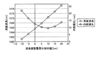
図4は、図3に示す構成の面発光レーザ素子における、波長調整層の厚さとレーザ発振波長または内部損失との関係の一例を示す図である。なお、波長調整層の厚さは、特定の面発光レーザ素子における波長調整層の厚さに対する相対的な厚さとして示している。図4に示すように、波長調整層の厚さを−10nmから20nmの合計30nmだけ変化させることによって、面発光レーザ素子のレーザ発振波長を約1061nmから約1075nmの間の約14nmの範囲で調整することができる。 FIG. 4 is a diagram showing an example of the relationship between the thickness of the wavelength adjustment layer and the laser oscillation wavelength or internal loss in the surface emitting laser element having the configuration shown in FIG. The thickness of the wavelength adjustment layer is shown as a relative thickness to the thickness of the wavelength adjustment layer in a specific surface emitting laser element. As shown in FIG. 4, by changing the thickness of the wavelength adjustment layer by a total of 30 nm from −10 nm to 20 nm, the laser oscillation wavelength of the surface emitting laser element is adjusted in a range of about 14 nm between about 1061 nm and about 1075 nm. can do.
なお、図4において、面発光レーザ素子のたとえば上部または下部DBRミラーを構成する各層の厚さは、特定のレーザ発振波長(図4においては、約1066nm)に対して最適化されている。図4では、波長調整層の厚さだけを変化させてレーザ発振波長を調整しているので、レーザ発振波長が上記最適化された波長から遠ざかると、光共振器内の内部損失が増大する。したがって、この内部損失の増大を考慮して調整すべき波長範囲を設定することが好ましい。たとえば、図4においては、内部損失の最小値からの増大量を15/cmまで許容すると、調整できる波長範囲は約1061nmから約1075nmの約14nmである。なお、波長1.1μm帯においては、光の周波数で200GHzの間隔は、波長に換算して0.7nmである。したがって、調整範囲の約14nmの間に、周波数200GHz間隔で約20チャネルのレーザ信号光を配列することができる。 In FIG. 4, the thickness of each layer constituting, for example, the upper or lower DBR mirror of the surface emitting laser element is optimized for a specific laser oscillation wavelength (about 1066 nm in FIG. 4). In FIG. 4, only the thickness of the wavelength adjustment layer is changed to adjust the laser oscillation wavelength. Therefore, when the laser oscillation wavelength is moved away from the optimized wavelength, the internal loss in the optical resonator increases. Therefore, it is preferable to set the wavelength range to be adjusted in consideration of this increase in internal loss. For example, in FIG. 4, if the increase from the minimum value of the internal loss is allowed to 15 / cm, the adjustable wavelength range is about 14 nm from about 1061 nm to about 1075 nm. In the wavelength band of 1.1 μm, the 200 GHz interval in terms of light frequency is 0.7 nm in terms of wavelength. Therefore, about 20 channels of laser signal light can be arranged at intervals of 200 GHz in the adjustment range of about 14 nm.
つぎに、図5は、図4に基づいて波長調整層の相対的な厚さを0nmから20nmまで変化させた5つの面発光レーザ素子における、バイアス電流とレーザ光の光強度の関係の一例を示す図である。これらの面発光レーザ素子は、レーザ発振波長が図4に示すように約10nmの範囲で分布しているが、いずれの波長においても、バイアス電流に対して直線性のよい安定した強度のレーザ光を出力することができる。 Next, FIG. 5 shows an example of the relationship between the bias current and the light intensity of the laser light in five surface emitting laser elements in which the relative thickness of the wavelength adjusting layer is changed from 0 nm to 20 nm based on FIG. FIG. These surface-emitting laser elements have a laser oscillation wavelength distributed in a range of about 10 nm as shown in FIG. 4, but at any wavelength, a laser beam having a stable intensity with good linearity with respect to a bias current. Can be output.
なお、波長調整層135−1〜135−nの厚さは、面発光レーザ素子130−1〜130−nの製造プロセスにおいて、波長調整層135−1〜135−nをエッチングする時間を調整することによって、きわめて高精度に調整できるので、レーザ信号光OS1−1〜OS1−nの波長も、所定の周波数間隔になるようにきわめて高精度に調整することができる。 The thickness of the wavelength adjustment layers 135-1 to 135-n adjusts the time for etching the wavelength adjustment layers 135-1 to 135-n in the manufacturing process of the surface emitting laser elements 130-1 to 130-n. As a result, the laser signal light OS1-1 to OS1-n can be adjusted with very high precision so as to have a predetermined frequency interval.
つぎに、図2に示した面発光レーザ素子130−1〜130−nが備える加熱機構について説明する。図6は、各面発光レーザ素子130−1〜130−nが備える加熱機構の模式的な平面図である。図6に示すように、この加熱機構は、上部DBRミラー136内のp側円環電極134上に配置された円環の一部を切り欠いた形状の高抵抗加熱部137と、アーム部137aを介して高抵抗加熱部137に接続した、高抵抗加熱部137よりも電気抵抗が低い低抵抗部138とを備えている。低抵抗部138は、隣接する面発光レーザ素子に備えられた高抵抗加熱部ともアーム部を介して連接している。
Next, a heating mechanism provided in the surface emitting laser elements 130-1 to 130-n shown in FIG. 2 will be described. FIG. 6 is a schematic plan view of a heating mechanism provided in each of the surface emitting laser elements 130-1 to 130-n. As shown in FIG. 6, this heating mechanism includes a high
なお、高抵抗加熱部137およびアーム部137aは、たとえば幅5μm、厚さ100nmの白金(Pt)の薄膜からなる。また、低抵抗部138は、たとえば幅10μm、厚さ2μmと比較的厚い金(Au)の薄膜からなる。
The high
この加熱機構は、各面発光レーザ素子130−1〜130−nのレーザ発振波長を一括して調整するためのものである。すなわち、この加熱機構の低抵抗部138を介して高抵抗加熱部137に電流を流すことによって、各面発光レーザ素子130−1〜130−nの活性層132aが加熱され、温度上昇するため、レーザ発振波長が変化する。なお、温度上昇に対するレーザ発振波長の変化の係数は、たとえば活性層132aが1.1μm帯のレーザ光用の半導体材料であるInGaAsなどのGaAs系材料からなる場合は約0.067nm/℃である。
This heating mechanism is for collectively adjusting the laser oscillation wavelengths of the surface emitting laser elements 130-1 to 130-n. That is, since the
ここで、各面発光レーザ素子130−1〜130−nの高抵抗加熱部137は、低抵抗部138によって直列接続しているので、低抵抗部138を介して所定値の電流を流した場合に各高抵抗加熱部137の温度上昇は等しくなる。その結果、各面発光レーザ素子130−1〜130−nのレーザ発振波長のシフト量も等しくなる。したがって、この加熱機構を用いれば、各面発光レーザ素子130−1〜130−nのレーザ発振波長を一括して調整することができる。このようにレーザ発振波長を一括して調整すれば、個別に調整する場合よりも電流の制御回路構成が簡易になり好ましい。
Here, since the high
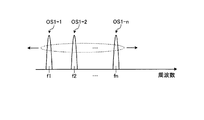
図7は、レーザ発振波長の一括調整を説明する図である。ここで、符号f1〜fnは、周波数軸上で等間隔に配置された周波数グリッドを示している。各面発光レーザ素子130−1〜130−nのレーザ信号光OS1−1〜OS1−nは、上述した波長調整層の厚さの調整によって、あらかじめ周波数グリッドf1〜fnの周波数間隔になるようにきわめて高精度に調整されている。そこで、図6に示すように加熱機構の消費電力を調整すれば、レーザ信号光OS1−1〜OS1−nの各波長を一括してシフトさせて、これらが周波数グリッドf1〜fnに一致するように調整することができる。 FIG. 7 is a diagram for explaining batch adjustment of laser oscillation wavelengths. Here, the symbols f1 to fn indicate frequency grids arranged at equal intervals on the frequency axis. The laser signal lights OS1-1 to OS1-n of the surface emitting laser elements 130-1 to 130-n are set to have frequency intervals of the frequency grids f1 to fn in advance by adjusting the thickness of the wavelength adjustment layer described above. It is adjusted with extremely high accuracy. Therefore, if the power consumption of the heating mechanism is adjusted as shown in FIG. 6, the wavelengths of the laser signal lights OS1-1 to OS1-n are collectively shifted so that they coincide with the frequency grids f1 to fn. Can be adjusted.
図8は、図6に示す加熱機構の消費電力とレーザ発振波長の波長シフトとの関係の一例を示す図である。図8に示すように、消費電力が20mW程度でレーザ発振波長を1.5nm程度だけ波長シフトさせることができる。 FIG. 8 is a diagram showing an example of the relationship between the power consumption of the heating mechanism shown in FIG. 6 and the wavelength shift of the laser oscillation wavelength. As shown in FIG. 8, the laser oscillation wavelength can be shifted by about 1.5 nm with power consumption of about 20 mW.
なお、上記実施の形態において、面発光レーザ素子のレーザ発振波長が1.0〜1.2μmであれば、1μm未満の波長帯に存在するシリコンの光吸収帯、およびGaAsの光吸収帯である0.85μm帯からはずれているため、低損失のシステムを実現できる。それとともに、特性のよいInGaAs系歪み多重量子井戸構造を面発光レーザ素子の活性層に使用できるので、面発光レーザ素子を低消費電力化することができ好ましい。 In the above embodiment, when the laser oscillation wavelength of the surface emitting laser element is 1.0 to 1.2 μm, the light absorption band of silicon and the light absorption band of GaAs exist in a wavelength band of less than 1 μm. Since it is out of the 0.85 μm band, a low-loss system can be realized. At the same time, an InGaAs-based strained multiple quantum well structure with good characteristics can be used for the active layer of the surface emitting laser element, which is preferable because the surface emitting laser element can be reduced in power consumption.
また、上記実施の形態における半導体集積素子、面発光レーザ素子、加熱機構等の構成は例示であって、本発明に係る光インターコネクションシステムにおいては、公知の半導体集積素子、面発光レーザ素子、加熱機構等を適宜利用することができる。たとえば、加熱機構については、上部DBRレーザの表面にヒータパターンを形成したものでもよい。 Further, the configurations of the semiconductor integrated device, the surface emitting laser device, the heating mechanism, etc. in the above embodiment are exemplifications. In the optical interconnection system according to the present invention, a known semiconductor integrated device, surface emitting laser device, heating A mechanism or the like can be used as appropriate. For example, the heating mechanism may be a heater pattern formed on the surface of the upper DBR laser.
1 シリコン基板
2 シリコン光導波路
3 光合波器
4 光分波器
100 半導体集積素子
110 演算処理装置
120 レーザ駆動装置
130 面発光レーザアレイ素子
130−1〜130−n 面発光レーザ素子
131 下部DBRミラー
132 半導体積層構造
132a 活性層
132b 電流狭窄層
133 n側電極
134 p側円環電極
135 波長調整層
136 上部DBRミラー
137 高抵抗加熱部
137a アーム部
138 低抵抗部
140 受光素子
150、160 光導波路
151 基部
152、154 クラッド部
153 コア部
153a 反射部
1000 光インターコネクションシステム
f1〜fn 周波数グリッド
I1 バイアス電流
I2 電流信号
I3 変調電流信号
OS1、OS1−1〜OS1−n、OS2 レーザ信号光
S 基板
S1 電圧信号
DESCRIPTION OF
Claims (8)
前記レーザ信号光を導波するシリコン光導波路と、
前記レーザ信号光を前記シリコン光導波路に結合させる光合波器と、
前記シリコン光導波路を導波する前記レーザ信号光を前記複数の半導体集積素子のうちの所定の半導体集積素子に結合させる光分波器と、
を備えることを特徴とする光インターコネクションシステム。 A plurality of surface-emitting laser array elements each having a plurality of surface-emitting laser elements that output laser signal lights having different wavelengths of 1.0 to 1.2 μm by direct modulation, and a plurality of semiconductor integrated elements each including a light-receiving array element;
A silicon optical waveguide for guiding the laser signal light;
An optical multiplexer for coupling the laser signal light to the silicon optical waveguide;
An optical demultiplexer for coupling the laser signal light guided through the silicon optical waveguide to a predetermined semiconductor integrated element among the plurality of semiconductor integrated elements;
An optical interconnection system comprising:
Priority Applications (4)
| Application Number | Priority Date | Filing Date | Title |
|---|---|---|---|
| JP2010157151A JP2012019157A (en) | 2010-07-09 | 2010-07-09 | Optical interconnection system |
| PCT/JP2011/003942 WO2012005012A2 (en) | 2010-07-09 | 2011-07-08 | Optical interconnection system |
| DE112011102307T DE112011102307T5 (en) | 2010-07-09 | 2011-07-08 | Optical connection system |
| US13/733,371 US8532155B2 (en) | 2010-07-09 | 2013-01-03 | Optical interconnection system |
Applications Claiming Priority (1)
| Application Number | Priority Date | Filing Date | Title |
|---|---|---|---|
| JP2010157151A JP2012019157A (en) | 2010-07-09 | 2010-07-09 | Optical interconnection system |
Publications (1)
| Publication Number | Publication Date |
|---|---|
| JP2012019157A true JP2012019157A (en) | 2012-01-26 |
Family
ID=44514908
Family Applications (1)
| Application Number | Title | Priority Date | Filing Date |
|---|---|---|---|
| JP2010157151A Pending JP2012019157A (en) | 2010-07-09 | 2010-07-09 | Optical interconnection system |
Country Status (4)
| Country | Link |
|---|---|
| US (1) | US8532155B2 (en) |
| JP (1) | JP2012019157A (en) |
| DE (1) | DE112011102307T5 (en) |
| WO (1) | WO2012005012A2 (en) |
Cited By (1)
| Publication number | Priority date | Publication date | Assignee | Title |
|---|---|---|---|---|
| JP2014041997A (en) * | 2012-07-23 | 2014-03-06 | Ricoh Co Ltd | Surface light-emitting laser element and atomic oscillator |
Families Citing this family (4)
| Publication number | Priority date | Publication date | Assignee | Title |
|---|---|---|---|---|
| EP2881773B1 (en) | 2013-12-03 | 2018-07-11 | ams AG | Semiconductor device with integrated mirror and method of producing a semiconductor device with integrated mirror |
| US10120149B1 (en) | 2017-07-13 | 2018-11-06 | Hewlett Packard Enterprise Development Lp | Wavelength division multiplexing (WDM) optical modules |
| WO2019014596A1 (en) * | 2017-07-14 | 2019-01-17 | Ours Technology, Inc. | Solid-state light detection and ranging system based on an optical phased array with an optical power distribution network |
| DE102020123558A1 (en) * | 2020-09-09 | 2022-03-10 | OSRAM Opto Semiconductors Gesellschaft mit beschränkter Haftung | SEMICONDUCTOR OPTOELECTRONIC DEVICE, SEMICONDUCTOR OPTOELECTRONIC DEVICE AND LIDAR SYSTEM |
Citations (7)
| Publication number | Priority date | Publication date | Assignee | Title |
|---|---|---|---|---|
| JP2000332229A (en) * | 1999-05-18 | 2000-11-30 | Canon Inc | PHOTOELECTRIC FUSION DEVICE STRUCTURE ON Si SUBSTRATE AND MANUFACTURE OF THE DEVICE |
| JP2005150298A (en) * | 2003-11-13 | 2005-06-09 | Seiko Epson Corp | Minute tile-like element, connecting structure, connecting method, thin film device, and electronic apparatus |
| JP2006073965A (en) * | 2004-09-06 | 2006-03-16 | Fuji Xerox Co Ltd | Manufacturing method of surface emitting laser diode and multiple-wavelength surface emitting laser diode, surface emitting laser diode, multiple-wavelength surface emitting laser diode, and optical communication system |
| JP2006526891A (en) * | 2003-06-05 | 2006-11-24 | ニコラエビチ レデンチョフ,ニコライ | Intelligent wavelength division multiplexing system based on tunable laser array and tunable resonant photodetector array |
| JP2006351692A (en) * | 2005-06-14 | 2006-12-28 | Fuji Xerox Co Ltd | Surface-emitting laser, its manufacturing method, and apparatus |
| US20080031294A1 (en) * | 2006-07-12 | 2008-02-07 | Krishnamoorthy Ashok V | Structures and methods for adjusting the wavelengths of lasers via temperature control |
| JP2008071829A (en) * | 2006-09-12 | 2008-03-27 | Toshiba Corp | Surface emitting semiconductor element |
Family Cites Families (8)
| Publication number | Priority date | Publication date | Assignee | Title |
|---|---|---|---|---|
| US7020400B2 (en) * | 1999-12-24 | 2006-03-28 | Altera Corporation | Multi-wavelength optical communication system |
| US6804283B2 (en) * | 2001-01-11 | 2004-10-12 | California Institute Of Technology | Compact electrically and optically pumped multi-wavelength nanocavity laser, modulator and detector arrays and method of making the same |
| US6603915B2 (en) * | 2001-02-05 | 2003-08-05 | Fujitsu Limited | Interposer and method for producing a light-guiding structure |
| US7418163B2 (en) * | 2002-03-28 | 2008-08-26 | Chakravorty Kishore K | Optoelectrical package |
| JP3987500B2 (en) * | 2004-02-17 | 2007-10-10 | 浜松ホトニクス株式会社 | Optical wiring board and method for manufacturing optical wiring board |
| JP2006351917A (en) | 2005-06-17 | 2006-12-28 | Nippon Telegr & Teleph Corp <Ntt> | Optical integrated circuit |
| JP2007214430A (en) | 2006-02-10 | 2007-08-23 | Fuji Xerox Co Ltd | Multimode optical communication system and multiwavelength surface emitting element |
| JP2010157151A (en) | 2008-12-29 | 2010-07-15 | Kan:Kk | System and method for analyzing access |
-
2010
- 2010-07-09 JP JP2010157151A patent/JP2012019157A/en active Pending
-
2011
- 2011-07-08 WO PCT/JP2011/003942 patent/WO2012005012A2/en active Application Filing
- 2011-07-08 DE DE112011102307T patent/DE112011102307T5/en not_active Ceased
-
2013
- 2013-01-03 US US13/733,371 patent/US8532155B2/en active Active
Patent Citations (7)
| Publication number | Priority date | Publication date | Assignee | Title |
|---|---|---|---|---|
| JP2000332229A (en) * | 1999-05-18 | 2000-11-30 | Canon Inc | PHOTOELECTRIC FUSION DEVICE STRUCTURE ON Si SUBSTRATE AND MANUFACTURE OF THE DEVICE |
| JP2006526891A (en) * | 2003-06-05 | 2006-11-24 | ニコラエビチ レデンチョフ,ニコライ | Intelligent wavelength division multiplexing system based on tunable laser array and tunable resonant photodetector array |
| JP2005150298A (en) * | 2003-11-13 | 2005-06-09 | Seiko Epson Corp | Minute tile-like element, connecting structure, connecting method, thin film device, and electronic apparatus |
| JP2006073965A (en) * | 2004-09-06 | 2006-03-16 | Fuji Xerox Co Ltd | Manufacturing method of surface emitting laser diode and multiple-wavelength surface emitting laser diode, surface emitting laser diode, multiple-wavelength surface emitting laser diode, and optical communication system |
| JP2006351692A (en) * | 2005-06-14 | 2006-12-28 | Fuji Xerox Co Ltd | Surface-emitting laser, its manufacturing method, and apparatus |
| US20080031294A1 (en) * | 2006-07-12 | 2008-02-07 | Krishnamoorthy Ashok V | Structures and methods for adjusting the wavelengths of lasers via temperature control |
| JP2008071829A (en) * | 2006-09-12 | 2008-03-27 | Toshiba Corp | Surface emitting semiconductor element |
Cited By (1)
| Publication number | Priority date | Publication date | Assignee | Title |
|---|---|---|---|---|
| JP2014041997A (en) * | 2012-07-23 | 2014-03-06 | Ricoh Co Ltd | Surface light-emitting laser element and atomic oscillator |
Also Published As
| Publication number | Publication date |
|---|---|
| US8532155B2 (en) | 2013-09-10 |
| WO2012005012A2 (en) | 2012-01-12 |
| DE112011102307T5 (en) | 2013-05-02 |
| US20130121354A1 (en) | 2013-05-16 |
| WO2012005012A3 (en) | 2012-04-26 |
Similar Documents
| Publication | Publication Date | Title |
|---|---|---|
| CN109075532B (en) | High speed VCSEL device | |
| US7835417B2 (en) | Narrow spectrum light source | |
| US6055262A (en) | Resonant reflector for improved optoelectronic device performance and enhanced applicability | |
| US6574398B2 (en) | Direct-coupled multimode WDM optical data links with monolithically-integrated multiple-channel VCSEL and photodetector arrays | |
| US6782027B2 (en) | Resonant reflector for use with optoelectronic devices | |
| US20040105476A1 (en) | Planar waveguide surface emitting laser and photonic integrated circuit | |
| JP2016178283A (en) | Wavelength variable laser element and laser module | |
| US20060127006A1 (en) | Tunable demultiplexer and tunable laser with optical deflector | |
| JP2009542033A (en) | Electrically pumped semiconductor evanescent laser | |
| CN108603980B (en) | Photonic integrated device with dielectric structure | |
| US20160315451A1 (en) | Tunable Optical Apparatus | |
| US8532155B2 (en) | Optical interconnection system | |
| US10816792B2 (en) | Wavelength tunable optical sources, filters and detectors | |
| JP3111957B2 (en) | Surface emitting device | |
| US20050036533A1 (en) | Tunable detector | |
| JP2012019158A (en) | Surface emitting laer element and surface emitting laer array element | |
| KR20230021622A (en) | Reflector for vcsel | |
| JP2011243650A (en) | Semiconductor laser element | |
| JP2012230949A (en) | Laser element array and manufacturing method thereof and optical interconnection system | |
| Fallahi et al. | WDM module research within the Canadian solid state optoelectronics consortium |
Legal Events
| Date | Code | Title | Description |
|---|---|---|---|
| A621 | Written request for application examination |
Free format text: JAPANESE INTERMEDIATE CODE: A621 Effective date: 20130524 |
|
| A131 | Notification of reasons for refusal |
Free format text: JAPANESE INTERMEDIATE CODE: A131 Effective date: 20140430 |
|
| A02 | Decision of refusal |
Free format text: JAPANESE INTERMEDIATE CODE: A02 Effective date: 20140902 |