JP2011198739A - Reduced flicker ac led lamp with separately shortable section of led string - Google Patents
Reduced flicker ac led lamp with separately shortable section of led string Download PDFInfo
- Publication number
- JP2011198739A JP2011198739A JP2010229359A JP2010229359A JP2011198739A JP 2011198739 A JP2011198739 A JP 2011198739A JP 2010229359 A JP2010229359 A JP 2010229359A JP 2010229359 A JP2010229359 A JP 2010229359A JP 2011198739 A JP2011198739 A JP 2011198739A
- Authority
- JP
- Japan
- Prior art keywords
- leds
- string
- voltage
- input
- led
- Prior art date
- Legal status (The legal status is an assumption and is not a legal conclusion. Google has not performed a legal analysis and makes no representation as to the accuracy of the status listed.)
- Granted
Links
Images


Classifications
-
- H—ELECTRICITY
- H05—ELECTRIC TECHNIQUES NOT OTHERWISE PROVIDED FOR
- H05B—ELECTRIC HEATING; ELECTRIC LIGHT SOURCES NOT OTHERWISE PROVIDED FOR; CIRCUIT ARRANGEMENTS FOR ELECTRIC LIGHT SOURCES, IN GENERAL
- H05B45/00—Circuit arrangements for operating light-emitting diodes [LED]
- H05B45/30—Driver circuits
-
- H—ELECTRICITY
- H05—ELECTRIC TECHNIQUES NOT OTHERWISE PROVIDED FOR
- H05B—ELECTRIC HEATING; ELECTRIC LIGHT SOURCES NOT OTHERWISE PROVIDED FOR; CIRCUIT ARRANGEMENTS FOR ELECTRIC LIGHT SOURCES, IN GENERAL
- H05B45/00—Circuit arrangements for operating light-emitting diodes [LED]
- H05B45/10—Controlling the intensity of the light
- H05B45/14—Controlling the intensity of the light using electrical feedback from LEDs or from LED modules
-
- H—ELECTRICITY
- H05—ELECTRIC TECHNIQUES NOT OTHERWISE PROVIDED FOR
- H05B—ELECTRIC HEATING; ELECTRIC LIGHT SOURCES NOT OTHERWISE PROVIDED FOR; CIRCUIT ARRANGEMENTS FOR ELECTRIC LIGHT SOURCES, IN GENERAL
- H05B45/00—Circuit arrangements for operating light-emitting diodes [LED]
- H05B45/40—Details of LED load circuits
- H05B45/44—Details of LED load circuits with an active control inside an LED matrix
- H05B45/48—Details of LED load circuits with an active control inside an LED matrix having LEDs organised in strings and incorporating parallel shunting devices
-
- H—ELECTRICITY
- H05—ELECTRIC TECHNIQUES NOT OTHERWISE PROVIDED FOR
- H05B—ELECTRIC HEATING; ELECTRIC LIGHT SOURCES NOT OTHERWISE PROVIDED FOR; CIRCUIT ARRANGEMENTS FOR ELECTRIC LIGHT SOURCES, IN GENERAL
- H05B45/00—Circuit arrangements for operating light-emitting diodes [LED]
- H05B45/50—Circuit arrangements for operating light-emitting diodes [LED] responsive to malfunctions or undesirable behaviour of LEDs; responsive to LED life; Protective circuits
- H05B45/54—Circuit arrangements for operating light-emitting diodes [LED] responsive to malfunctions or undesirable behaviour of LEDs; responsive to LED life; Protective circuits in a series array of LEDs
-
- H—ELECTRICITY
- H05—ELECTRIC TECHNIQUES NOT OTHERWISE PROVIDED FOR
- H05B—ELECTRIC HEATING; ELECTRIC LIGHT SOURCES NOT OTHERWISE PROVIDED FOR; CIRCUIT ARRANGEMENTS FOR ELECTRIC LIGHT SOURCES, IN GENERAL
- H05B45/00—Circuit arrangements for operating light-emitting diodes [LED]
- H05B45/50—Circuit arrangements for operating light-emitting diodes [LED] responsive to malfunctions or undesirable behaviour of LEDs; responsive to LED life; Protective circuits
- H05B45/59—Circuit arrangements for operating light-emitting diodes [LED] responsive to malfunctions or undesirable behaviour of LEDs; responsive to LED life; Protective circuits for reducing or suppressing flicker or glow effects
-
- H—ELECTRICITY
- H05—ELECTRIC TECHNIQUES NOT OTHERWISE PROVIDED FOR
- H05B—ELECTRIC HEATING; ELECTRIC LIGHT SOURCES NOT OTHERWISE PROVIDED FOR; CIRCUIT ARRANGEMENTS FOR ELECTRIC LIGHT SOURCES, IN GENERAL
- H05B45/00—Circuit arrangements for operating light-emitting diodes [LED]
- H05B45/30—Driver circuits
- H05B45/31—Phase-control circuits
-
- H—ELECTRICITY
- H05—ELECTRIC TECHNIQUES NOT OTHERWISE PROVIDED FOR
- H05B—ELECTRIC HEATING; ELECTRIC LIGHT SOURCES NOT OTHERWISE PROVIDED FOR; CIRCUIT ARRANGEMENTS FOR ELECTRIC LIGHT SOURCES, IN GENERAL
- H05B45/00—Circuit arrangements for operating light-emitting diodes [LED]
- H05B45/30—Driver circuits
- H05B45/345—Current stabilisation; Maintaining constant current
-
- H—ELECTRICITY
- H05—ELECTRIC TECHNIQUES NOT OTHERWISE PROVIDED FOR
- H05B—ELECTRIC HEATING; ELECTRIC LIGHT SOURCES NOT OTHERWISE PROVIDED FOR; CIRCUIT ARRANGEMENTS FOR ELECTRIC LIGHT SOURCES, IN GENERAL
- H05B45/00—Circuit arrangements for operating light-emitting diodes [LED]
- H05B45/30—Driver circuits
- H05B45/355—Power factor correction [PFC]; Reactive power compensation
-
- H—ELECTRICITY
- H05—ELECTRIC TECHNIQUES NOT OTHERWISE PROVIDED FOR
- H05B—ELECTRIC HEATING; ELECTRIC LIGHT SOURCES NOT OTHERWISE PROVIDED FOR; CIRCUIT ARRANGEMENTS FOR ELECTRIC LIGHT SOURCES, IN GENERAL
- H05B45/00—Circuit arrangements for operating light-emitting diodes [LED]
- H05B45/30—Driver circuits
- H05B45/36—Circuits for reducing or suppressing harmonics, ripples or electromagnetic interferences [EMI]
-
- H—ELECTRICITY
- H05—ELECTRIC TECHNIQUES NOT OTHERWISE PROVIDED FOR
- H05B—ELECTRIC HEATING; ELECTRIC LIGHT SOURCES NOT OTHERWISE PROVIDED FOR; CIRCUIT ARRANGEMENTS FOR ELECTRIC LIGHT SOURCES, IN GENERAL
- H05B45/00—Circuit arrangements for operating light-emitting diodes [LED]
- H05B45/30—Driver circuits
- H05B45/395—Linear regulators
-
- H—ELECTRICITY
- H05—ELECTRIC TECHNIQUES NOT OTHERWISE PROVIDED FOR
- H05B—ELECTRIC HEATING; ELECTRIC LIGHT SOURCES NOT OTHERWISE PROVIDED FOR; CIRCUIT ARRANGEMENTS FOR ELECTRIC LIGHT SOURCES, IN GENERAL
- H05B45/00—Circuit arrangements for operating light-emitting diodes [LED]
- H05B45/50—Circuit arrangements for operating light-emitting diodes [LED] responsive to malfunctions or undesirable behaviour of LEDs; responsive to LED life; Protective circuits
- H05B45/56—Circuit arrangements for operating light-emitting diodes [LED] responsive to malfunctions or undesirable behaviour of LEDs; responsive to LED life; Protective circuits involving measures to prevent abnormal temperature of the LEDs
-
- Y—GENERAL TAGGING OF NEW TECHNOLOGICAL DEVELOPMENTS; GENERAL TAGGING OF CROSS-SECTIONAL TECHNOLOGIES SPANNING OVER SEVERAL SECTIONS OF THE IPC; TECHNICAL SUBJECTS COVERED BY FORMER USPC CROSS-REFERENCE ART COLLECTIONS [XRACs] AND DIGESTS
- Y02—TECHNOLOGIES OR APPLICATIONS FOR MITIGATION OR ADAPTATION AGAINST CLIMATE CHANGE
- Y02B—CLIMATE CHANGE MITIGATION TECHNOLOGIES RELATED TO BUILDINGS, e.g. HOUSING, HOUSE APPLIANCES OR RELATED END-USER APPLICATIONS
- Y02B20/00—Energy efficient lighting technologies, e.g. halogen lamps or gas discharge lamps
- Y02B20/30—Semiconductor lamps, e.g. solid state lamps [SSL] light emitting diodes [LED] or organic LED [OLED]
Landscapes
- Circuit Arrangement For Electric Light Sources In General (AREA)
- Led Devices (AREA)
Abstract
Description
本出願は、その主題が参照により本明細書に組み込まれる、2010年3月19日に出願された「AC LED Lamp Involving An LED String Having Separately Shortable Sections」という名称の仮米国特許出願番号12/661,603の一部継続出願であり、かつ、米国特許法第120条の下でのそれからの優先権を主張する。
This application is a provisional US patent application Ser. No. 12/661, entitled “AC LED Lamp Involving An LED String Having Separated Sections,” filed Mar. 19, 2010, the subject matter of which is incorporated herein by reference. , 603, a continuation-in-part application, and claims priority from it under
本開示は、一般に、発光ダイオード(「LED」)給電、制御、および保護回路に関し、より具体的には、交流(「AC」)駆動式LED給電、制御、および保護回路に関する。 The present disclosure relates generally to light emitting diode (“LED”) power supply, control, and protection circuits, and more specifically to alternating current (“AC”) driven LED power supply, control, and protection circuits.
発光ダイオードまたは「LED」は、汎用照明のために益々使用されている。一例では、いわゆる白色LEDのグループは、AC電力源から給電給される。用語「AC LED」は、こうした回路を指すのに使用されることがある。並列接続されたLEDの対向するストリングを利用するAC LED回路は、米国特許第5,495,147号、6,830,358号、7,045,965号、7,138,770号、7,264,381号、および7,344,275号に記載される。ブリッジ整流式LEDストリングを含むAC LED回路は、米国特許第5,463,280号および7,276,858号に記載される。米国特許出願公報US2007/0008721は、複数の方法で接続された並列接続されたAC LEDのネットワークを示す。 Light emitting diodes or “LEDs” are increasingly used for general purpose lighting. In one example, a group of so-called white LEDs is powered from an AC power source. The term “AC LED” may be used to refer to such a circuit. AC LED circuits utilizing opposing strings of LEDs connected in parallel are described in US Pat. Nos. 5,495,147, 6,830,358, 7,045,965, 7,138,770, 7, 264,381 and 7,344,275. AC LED circuits including bridged rectifier LED strings are described in US Pat. Nos. 5,463,280 and 7,276,858. US Patent Application Publication US2007 / 0008721 shows a network of AC LEDs connected in parallel in multiple ways.
図1(従来技術)は、AC−DC変換器も整流器も必要としない1つのAC LEDランプ回路の図である。DC電圧が供給されうるが、AC電圧が、通常、入力端子1と2との間に供給される。端子1および2は、たとえば、110V ACライン電力を受けるために結合されてもよい。端子1上の電圧が、端子2上の電圧より高い場合、電流は、端子1から電流制限抵抗器3を通りノード4へ、次に、直列接続されたLED5の第1のストリングを通りノード6へ、次に、電流制限抵抗器7を通り端子2へ流れる。端子1上の電圧が、端子2上の電圧より低い場合、電流は、反対方向に、端子2から電流制限抵抗器7を通りノード6へ、直列接続されたLED8の第2のストリングを通りノード4へ、次に、電流制限抵抗器3を通り端子1へ流れる。
FIG. 1 (prior art) is a diagram of one AC LED lamp circuit that does not require an AC-DC converter or rectifier. A DC voltage can be supplied, but an AC voltage is usually supplied between the
図2(従来技術)は、第2のAC LEDランプ回路の図である。この回路は、全波整流器9を使用する。DCまたはAC入力は、端子10および11で受電される。端子10および11は、たとえば、110V ACライン電力を受電するように結合され得る。到来AC入力の各半サイクルで、両方のLEDストリング12および13が光を発するが、全波整流器9を設けるという余分のコストが必要とされる。図1の回路の場合にそうであるように、電流は、電流制限抵抗器14および15で制限される。
FIG. 2 (Prior Art) is a diagram of a second AC LED lamp circuit. This circuit uses a
図1および2のAC LED回路の効率的な使用は、一般に、安定性を確保するために、LEDでの電圧降下に対して、ラインのAC電圧を良好に制御して整合させることの必要や、および/または、ライン電圧またはLED電圧降下が変化するときの電流変動を制限するために図示すような電流制限抵抗器の付加することの必要がある。電流制限抵抗器手法の欠点は、電力損失である。この電力損失は、LEDランプの低い効率および高い熱発生をもたらす。 Efficient use of the AC LED circuit of FIGS. 1 and 2 generally requires that the line AC voltage be well controlled and matched to the voltage drop at the LED to ensure stability. And / or the need to add a current limiting resistor as shown to limit current fluctuations when the line voltage or LED voltage drop changes. The disadvantage of the current limiting resistor approach is power loss. This power loss results in low efficiency and high heat generation of the LED lamp.
図2の回路の110V AC動作例では、625オーム実効抵抗が、110V ACおよび40ミリアンペアRMSで動作するLEDストリングと直列に配設される。これは、4ワットLEDランプの場合、1ワットの抵抗性電力損失をもたらす。これは、26%の効率損失になる。220V AC動作例では、2.5kオーム実効抵抗が、220V ACおよび20ミリアンペアRMSで動作するLEDストリングと直列に配設される。これは、4ワットLEDランプの場合、1ワットの抵抗性電力損失をもたらす。これは、26%の効率損失になる。電流制限抵抗器の両端のRMS電圧降下は、ACラインRMS電圧の約26%であるため、ACライン電圧の10%の増加が、LED電流の約40%(10%/26%)の増加をもたらす。LED電流のこの増加は、抵抗にわたる70%多い電力損失をもたらし、熱消散の増加をもたらし、電力消費の約50%の増加をもたらす。同様に、ライン電圧の10%の低減は、LED電流の観測可能な36%の低下をもたらす。 In the 110V AC operation example of the circuit of FIG. 2, a 625 ohm effective resistance is placed in series with the LED string operating at 110V AC and 40 milliamps RMS. This results in a resistive power loss of 1 watt for a 4 watt LED lamp. This results in an efficiency loss of 26%. In the 220V AC operation example, a 2.5k ohm effective resistance is placed in series with the LED string operating at 220V AC and 20 milliamps RMS. This results in a resistive power loss of 1 watt for a 4 watt LED lamp. This results in an efficiency loss of 26%. Since the RMS voltage drop across the current limiting resistor is about 26% of the AC line RMS voltage, a 10% increase in AC line voltage will result in an approximately 40% (10% / 26%) increase in LED current. Bring. This increase in LED current results in 70% more power loss across the resistance, resulting in increased heat dissipation and an approximately 50% increase in power consumption. Similarly, a 10% reduction in line voltage results in an observable 36% drop in LED current.
こうした抵抗性電力損失を回避するために、キャパシタ結合式AC LEDが提案された。たとえば、米国特許第6,972,528号および7,489,086号は、並列接続された対向するLED対に直列接続した、高周波分離用のキャパシタを使用することを開示する。この手法の欠点は、値の高いキャパシタを提供する必要性である。別の欠点は、安定したdV/dtに依存することおよびトライアック調光器と一般的な互換性がないことである。こうした回路は、高周波AC供給源コントローラで駆動され得るが、そうすることは、高周波ドライバ用の複雑な回路要素を必要とする。 In order to avoid such resistive power loss, a capacitor coupled AC LED has been proposed. For example, US Pat. Nos. 6,972,528 and 7,489,086 disclose the use of high frequency isolation capacitors connected in series with opposing LED pairs connected in parallel. The disadvantage of this approach is the need to provide a high value capacitor. Another drawback is the dependence on stable dV / dt and the lack of general compatibility with triac dimmers. Such circuits can be driven with a high frequency AC source controller, but doing so requires complex circuit elements for the high frequency driver.
米国特許第6,577,072号は、貯蔵キャパシタと並列接続されたLEDのストリングに接続されたスイッチを備える非モノリシック回路要素を使用する別の手法を述べる。スイッチは、ライン電圧があるレベルより下がるとターンオフするため、LEDは、キャパシタによって給電される。排出されたキャパシタがスイッチを通して再充電することを必要とするため、これは、損失無し手法ではない。さらに、LEDの光出力は、ライン電圧の変化に対して調節されない。 US Pat. No. 6,577,072 describes another approach that uses a non-monolithic circuit element with a switch connected to a string of LEDs connected in parallel with a storage capacitor. Since the switch turns off when the line voltage drops below a certain level, the LED is powered by a capacitor. This is not a lossless approach because the drained capacitor needs to be recharged through the switch. Furthermore, the light output of the LED is not adjusted for changes in line voltage.
本発明は、電力損失を低減させたAC LEDランプを実現する技術を提供することにある。 It is an object of the present invention to provide a technique for realizing an AC LED lamp with reduced power loss.
AC LEDランプは、整流器、集積回路、および直列接続されたLEDのストリングを含む。AC LEDランプは、到来するAC信号(即ちAC入力)を受電し、受電したAC信号(AC入力)の整流をしたものがLEDストリングに印加されるようにして、受電したAC信号(AC入力)から電力供給がされる。集積回路は、複数の電力スイッチを含む。各電力スイッチは、LEDストリング内のLEDの複数のグループのうちの対応する1つのグループを、別々ににかつ選択可能に短絡させて除外し得るように結合される。グループは、LEDストリングのセクションとも呼ばれる。LEDストリングにわたる電圧が増加するにつれて、集積回路は、通電されるLEDの総数が増加するように、電力スイッチを制御する。ストリングにわたる電圧が減少するにつれて、集積回路は、通電するLEDの総数が減少するように、電力スイッチを制御する。 AC LED lamps include a rectifier, an integrated circuit, and a string of LEDs connected in series. The AC LED lamp receives an incoming AC signal (i.e., AC input), and a rectified version of the received AC signal (AC input) is applied to the LED string so that the received AC signal (AC input) is received. Power is supplied from. The integrated circuit includes a plurality of power switches. Each power switch is coupled such that a corresponding one of a plurality of groups of LEDs in the LED string can be separately and selectively shorted out. Groups are also referred to as LED string sections. As the voltage across the LED string increases, the integrated circuit controls the power switch so that the total number of energized LEDs increases. As the voltage across the string decreases, the integrated circuit controls the power switch so that the total number of energized LEDs decreases.
AC LEDランプでは、通電するLEDの総数およびLEDストリングの電流値は、優れた効率、信頼性、フリッカ防止性、ライン電圧変動に対する調節、電力力率の補正、ランプ過電圧保護、ランプ過電流保護、およびランプ過温度保護が提供できるように、制御され、調節される。開示されるランプ・アーキテクチャを使用することは、電解キャパシタを全く含まず、かつ、単に比較的少数のコンポーネントを含む、効率が高い固体AC LEDランプが実現されることを可能にする。電解キャパシタの使用の回避は、電解キャパシタがAC LEDランプに含まれる場合には普通なら信頼性を低下される可能性がある電解キャパシタ故障の問題を防止する。低減されたコンポーネント数は、ランプ信頼性を改善し、ランプの平均故障間隔を延ばす。電磁干渉(EMI)問題は、多くのAC−DC変換器LEDランプと比較して、最小になる。その理由は、本明細書で述べる新規のAC LEDランプが、高周波電力スイッチングを必要としないからである。 In AC LED lamps, the total number of energized LEDs and LED string current values are excellent efficiency, reliability, anti-flicker, adjustment to line voltage fluctuations, power factor correction, lamp overvoltage protection, lamp overcurrent protection, And controlled and regulated to provide lamp over-temperature protection. Using the disclosed lamp architecture allows a highly efficient solid state AC LED lamp to be realized that does not include any electrolytic capacitors and that simply includes a relatively small number of components. Avoidance of the use of electrolytic capacitors prevents the problem of electrolytic capacitor failure that would otherwise be unreliable if the electrolytic capacitor was included in an AC LED lamp. The reduced number of components improves lamp reliability and extends the average lamp failure time. Electromagnetic interference (EMI) problems are minimized compared to many AC-DC converter LED lamps. The reason is that the novel AC LED lamp described herein does not require high frequency power switching.
別の実施形態では、AC LEDランプは、フリッカ防止モードで動作する。LED電流が流れる直列接続のLEDのストリング内のLEDの数は、変化する電圧の信号(入力)の電圧振幅がピーク値へと増加するにつれて増加する。そして、LED電流が流れる直列接続のLEDのストリング内のLEDの数は、変化する電圧の信号(入力)の電圧振幅がピーク値から減少するにつれて減少する。光強度の複数のピークを生成するために、サイクル期間中のLED電流は、サイクル期間の12%未満の継続時間の間に、変化する電圧の入力の瞬時電流値の半分以上を低減される。 In another embodiment, the AC LED lamp operates in an anti-flicker mode. The number of LEDs in a string of series connected LEDs through which the LED current flows increases as the voltage amplitude of the changing voltage signal (input) increases to a peak value. Then, the number of LEDs in the string of series-connected LEDs through which the LED current flows decreases as the voltage amplitude of the changing voltage signal (input) decreases from the peak value. In order to produce multiple peaks of light intensity, the LED current during the cycle is reduced by more than half of the instantaneous current value of the changing voltage input for a duration of less than 12% of the cycle period.
なお別の実施形態では、AC LEDランプは、第2のフリッカ防止モードで動作する。LED電流が流れる直列接続のLEDのストリング内のLEDの数は、変化する電圧の信号(入力)の電圧振幅がピーク値へと増加するにつれて増加する。そして、LED電流が流れるLEDのストリング内のLEDの数は、変化する電圧の入力の電圧振幅がピーク値から減少するにつれて減少する。光強度の複数のピークを生成するために、LEDストリングの端部に接続された谷充填キャパシタは、それを変化する電圧の入力に結合することによって、変化する電圧の信号(入力)の電圧振幅が増加するにつれて、充電される。そして、谷充填キャパシタは、変化する電圧の信号(入力)の電圧振幅がピーク値の90%以上に達すると(第1の時点)、変化する電圧の入力から分離される。そして、谷充填キャパシタは、変化する電圧の信号(入力)の電圧振幅が谷電圧閾値より下がると、変化する電圧の信号(入力)に結合され、それにより、光強度のピークが生成される。 In yet another embodiment, the AC LED lamp operates in a second anti-flicker mode. The number of LEDs in a string of series connected LEDs through which the LED current flows increases as the voltage amplitude of the changing voltage signal (input) increases to a peak value. And the number of LEDs in the string of LEDs through which the LED current flows decreases as the voltage amplitude of the changing voltage input decreases from the peak value. To generate multiple peaks of light intensity, a valley-filled capacitor connected to the end of the LED string couples it to the changing voltage input, thereby changing the voltage amplitude of the changing voltage signal (input). As it increases, it is charged. The valley filling capacitor is separated from the changing voltage input when the voltage amplitude of the changing voltage signal (input) reaches 90% or more of the peak value (first time point). The valley-filled capacitor is then coupled to the changing voltage signal (input) when the voltage amplitude of the changing voltage signal (input) falls below the valley voltage threshold, thereby generating a light intensity peak.
他の構造および方法が、以下の詳細な説明で述べられる。本要約は、本発明を規定することを意図しない。本発明は、特許請求の範囲によって規定される。 Other structures and methods are described in the detailed description below. This summary is not intended to define the invention. The invention is defined by the claims.
同じ番号が同じコンポーネントを示す添付図面は、本発明の実施形態を示す。 The accompanying drawings, in which like numerals indicate like components, illustrate embodiments of the invention.
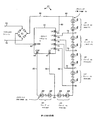
図3は、第1の実施形態によるAC LEDランプ50の回路図である。AC LEDランプ50は、全波整流器51、LEDランプ・レギュレータ集積回路(制御集積回路とも呼ばれる)52、および直列接続されたLEDのストリングを含む。整流器51は、示すように、入力電力端子53および54に接続される。ACまたはDCライン・イン電力入力が端子53および54上で受電される。
FIG. 3 is a circuit diagram of the
LEDストリングは、第1の端部55および第2の端部56を有する。LEDストリングは、次に、いくつかのセクション57〜62を含む。セクションは、本明細書でLEDのグループとも呼ばれる。種々のLEDグループ間の示されるノードは、本明細書において技術的でない意味で曖昧に相互接続ノードと呼ばれる。図3に示すように、LEDストリングの第2の端部56は、導体63を介してCSP端子64に結合され、LEDストリングの相互接続ノード65は、導体66を介して集積回路52のL0端子67に結合され、LEDストリングの相互接続ノード68は、導体69を介して集積回路52のL1端子70に結合され、相互接続ノード71は、導体72を介して集積回路52のL2端子73に結合され、相互接続ノード74は、導体75を介して集積回路52のL3端子76に結合され、相互接続ノード77は、導体78を介して集積回路52のL4端子79に結合され、LEDストリングの第1の端部55は、導体80を介して集積回路52のL5端子81に結合される。
The LED string has a
AC LEDランプ50は、ACまたはDCライン・イン電力入力によって入力電力端子53および54において給電される。ACライン・イン入力は、たとえば、110ボルトを有する60HzのAC正弦波であってよい。このACライン・イン入力は、全波整流器51によって整流され、整流されたライン電圧入力が、VSS端子82とL5端子81との間に、変化する電圧の信号(入力)として現れる。参照番号80は、整流器51からL5端子81まで、そして、LEDストリングの第1の端部55まで延在する導体およびノードを表す。正しい動作条件下で、集積回路52は、電流が、LEDストリングのLEDの種々の選択されたグループを通り、次に、集積回路52を通り、次に、VSS端子82から出て、整流器51に戻るように流れることを可能にする。集積回路52は、選択的に、LEDの選択されたグループを短絡させて除外し、LEDの選択されたグループを切換え投入して、LEDストリング電流経路内のLEDの数を変更し、それにより、LEDストリング全体の電流および電力を調節する。たとえば、入力電力端子53および54上の110V ACライン・イン正弦波AC入力の単一のサイクルでは、0°位相から360°位相まで変化する電圧の振幅を呈する。波形の0°の時には、導体80上の入力の(整流されたACラインの電圧に対応する)電圧は、最小値から、増加するか増加し始める。導体80の電圧は、0°位相のこの時点から、90°位相の時点まで増加する。この最初の90°の経過時間中、電流が流れ得るLEDの総数は、LEDストリングにわたる順方向電圧降下が、整流された瞬時ライン電圧に本質的に一致するように増加させられる。その後、導体80上の電圧が、90°位相の時点から180°位相の時点まで減少するにつれて、電流が流れ得るLEDの総数は、LEDストリングにわたる順方向電圧降下が、整流された瞬時ライン電圧に本質的に一致するように減少させられる。整流されたライン電圧が増減するときに、(たとえば、短絡除外される任意のLEDグループを含む端部55〜端部56の)全LEDストリングにわたる電圧降下を、導体80上の整流された瞬時ライン電圧に実質的に一致させることによって、優れたランプ効率が達成される。AC LEDランプ50の平均効率損失は、ライン電圧と比較して最も小さなLEDグループにわたる電圧降下の約半分に等しい。
The
図4は、図3のAC LEDランプ50の集積回路52をさらに詳細に示す図である。端子64、67、70、73、76、79、および81に加えて、集積回路52は、電力スイッチ83〜88、保護電力スイッチ89、電流センス抵抗器90、内部電源回路91、コントローラ回路92、およびデコーダ93を含む。電力スイッチ83は、CSP端子64をL0端子67に結合するように制御され、それにより、LEDグループ57を短絡させて除外することができ、電力スイッチ84は、L0端子67をL1端子70に結合するように制御され、それにより、LEDグループ58を短絡除外することができ、電力スイッチ85は、L1端子70をL2端子73に結合するように制御され、それにより、LEDグループ59を短絡除外することができ、電力スイッチ86は、L2端子73をL3端子76に結合するように制御され、それにより、LEDグループ60を短絡除外することができ、電力スイッチ87は、L3端子76をL4端子79に結合するように制御され、それにより、LEDグループ61を短絡除外することができ、電力スイッチ88は、L4端子79をL5端子81に結合するように制御され、それにより、LEDグループ62を短絡除外することができる。電力スイッチ83〜88は、コントローラ92およびデコーダ93によって個々に制御される。内部給電回路91は、内部VCC供給電圧(図示せず)を生成し、その内部供給電圧をコントローラ92およびデコーダ93に供給して、これらのブロック内の回路要素に電力供給する。コントローラ92は、6ビット・デジタルLEDCOUNT信号94を6ビット・バス95に供給する。LEDCOUNT信号は、LEDストリング全体での順方向電圧降下が、所望の平均LED電流レベルで導体80の整流されたライン電圧に一致するために、通電を許容されるべき(LEDストリング中の)LEDの最適数を示す。LEDストリングを通る電流は、電流センス抵抗器90によって検出される。デコーダ93は、LEDCOUNT信号を、電力スイッチ83〜88のゲートを駆動するための適切なゲートドライブ信号に変換するため、指示された数のLEDが、LEDストリング電流経路に切換え投入される。
FIG. 4 shows in more detail the
通常動作中、保護スイッチ89は、最小オン抵抗を有し、また、LEDストリング電流経路を整流器51へと戻すべく閉路をするように、ターンオンする。しかし、電流が大きい条件下では、保護スイッチ89のゲート上の電圧は、電流を所定の電流制限値に制限するように調整される。以下でさらに詳細に説明されるように、異常な動作条件下では、保護スイッチ89は、電流がLEDストリングを通って流れないように、また、LEDストリングが損傷から保護されるよう、開路するように制御される。
During normal operation, the
110V AC用では、LEDストリングは、直列に結合された約40〜50の白色LEDを含み、一方、220V AC用では、LEDストリングは、直列に結合された約80〜100の白色LEDを含む。示すように、これらのLEDは、それぞれ、N、2N、4N、8N、および16NのLEDの5つのグループに分割される。最後のグループ62は、残りのPのLEDを含むため、(31N+P)は、LEDストリング内のLEDの総数に等しい。 For 110V AC, the LED string includes approximately 40-50 white LEDs coupled in series, while for 220V AC, the LED string includes approximately 80-100 white LEDs coupled in series. As shown, these LEDs are divided into five groups of N, 2N, 4N, 8N, and 16N LEDs, respectively. Since the last group 62 includes the remaining P LEDs, (31N + P) is equal to the total number of LEDs in the LED string.
図5は、図4のコントローラ92のより詳細な図である。LEDCOUNT信号94は、アップ/ダウン・カウンタ122の出力である。導体およびノード80上の整流された瞬時ライン電圧がパワー・オン・リセット閾値(PORT)より小さいとき、パワー・オン・リセット回路96は、リセット信号97をアサートする。リセット信号97は、アップ/ダウン・カウンタ122を最大カウント状態にリセットする。カウンタ122をこの最大カウント状態に設定することは、突然のライン電圧ステップ(調光器トライアックがターンオンすることなどによる)が、LEDストリングにわたる制限された初期電流をもたらすことを確実にする。アップ信号98は、デジタル「ロー(low)」に設定される。整流された瞬時ライン電圧が、PORT閾値電圧より大きい場合、集積回路52は、整流されたライン電圧に一致する初期LEDCOUNTを見出すために最初の調整を行う。これを行うために、アップ/ダウン・カウンタ122は、適切な電流がLEDを通って流れていることを電流センス信号99が示すまで、カウントダウンする。電流センス信号99は、電流センス抵抗器90の両端で降下した電圧である。
FIG. 5 is a more detailed view of the
この時点で、アップ信号98は、デジタル「ハイ(high)」に設定され、回路は、ライン電圧包絡線にいつでも追従し始めることができる。アップ/ダウン・カウンタ122は、オンチップ・クロック発生器100によって供給されるクロック信号CLKによって決まるレートで増分されるかまたは減分される。整流されたライン電圧が増加していることを位相制御回路101が検出する場合、アップ信号98は、「ハイ」であり、一方、整流されたライン電圧が減少していることを位相制御回路が検出する場合、アップ信号98は、「ロー」である。アップ信号98が「ハイ」である(整流ライン電圧の増加)場合で、かつ、アップ/ダウン・カウンタ122のイネーブル入力102上に供給されるイネーブル信号がアサートされる場合、アップ/ダウン・カウンタ122は、クロック信号CLKの次の立上りエッジで増分する。イネーブル信号は、電流センス信号99が電流センス閾値信号104電圧(CSTS)を超えていることをアップ/ダウン比較器103が検出したときはいつでも、その条件が存在しなくなるまでアサートされる。アップ信号98が「ハイ」であり、イネーブル信号がアサートされていて、立上りクロック・エッジが生じると、LEDCOUNTの増分をする。LEDCOUNTの増分は、LEDストリング電流経路により多くのLEDを切換え投入できることを意味する。
At this point, the up
一方、アップ信号98が「ロー」である場合、CSTS信号104からVHYSTヒステリシス電圧105を引いた値より電流センス信号99が低いことをアップ/ダウン比較器103が検出したときはいつでも、その条件が存在しなくなるまで、アップ/ダウン・カウンタ122は、クロック信号CLKの次の立上りエッジで減分する。LEDCOUNTを減分することは、LEDストリング電流経路からLEDを切換え除外していくことを意味する。
On the other hand, when the up
集積増幅器回路106は、増幅器107およびキャパシタ108を含む。集積増幅器回路106は、スケーラ109によって変調された信号99の瞬時電圧と参照110によって供給されるVPAVG参照電圧との電圧差を線形増幅する。増幅された差は、キャパシタ108上で積分されて、エラー信号111が生成される。エラー信号111は、平均LED電力がターゲットLED電力より低い場合、漸増し、平均LED電力がターゲットLED電力より高い場合、漸減する。したがって、LEDストリングの平均LED電力は、(SCALE・VF・VPAVG/R90)へと調節される。ここで、SCALEは、スケーラ109およびLEDのグループ内のLEDの数に応じた定数であり、R90は、電流センス抵抗器90の抵抗値である。
標準的なトライアック調光器を含む用途で回路を動作させるために、VPAVGは、検出された調光器位相カット角によって調整される。標準的なトライアック調光器回路では、トライアックは、照明負荷に供給される全電力を低減するために、到来するAC入力の部分または整流されたライン入力の部分を開回路にしてもよい。図5の回路では、位相制御回路101は、本明細書では調光器「位相カット角」と呼ぶ、この開回路継続時間の位相を検出する。位相制御回路101は、位相カットが大きくなればなるほど、平均LED電力が小さくなるように、相応してVPAVGを調整する。
To operate the circuit in an application that includes a standard triac dimmer, the VPAVG is tuned by the detected dimmer phase cut angle. In a standard triac dimmer circuit, the triac may open the incoming AC input portion or rectified line input portion to reduce the total power delivered to the lighting load. In the circuit of FIG. 5, the
アップ/ダウン比較器103用の電流センス閾値信号104は、スケーラ112によって変調された、キャパシタ108からのエラー信号111である。スケーラ112は、LEDCOUNT信号94によって制御される。スケーラ109および112は、たとえば、抵抗器ラダーとして実現されてもよく、スケーラの制御信号によって制御されるアナログ・マルチプレクサを通して抵抗器ラダーの選択されたタップ上の信号が出力される。LEDCOUNTが小さな値である場合、スケーラ112は、小さな量だけエラー信号111をスケーリングし、一方、LEDCOUNTが大きな値である場合、スケーラ112は、エラー信号111を大きな量だけスケーリングする。瞬時LEDストリング電流を、その大きさが、直列接続されたLEDの数にほぼ比例して変わるようにスケーリングすることによって、ACサイクルにわたるLEDストリング電流の位相角は、電圧降下(LEDストリングにわたる電圧降下)信号の位相角に対して調整される。したがって、LEDランプの力率が調整され、ほぼ1になる。
The current
コントローラ92は、保護スイッチ89を制御する保護ゲート信号113(NPROT)をも生成する。通常の動作条件では、保護ゲート信号113は、バッファ115を通して電流制限増幅器114によって駆動される。電流センス信号99が、電圧源116によって設定されたVILIM閾値より小さいと、電流制限増幅器114は、NPROT信号113を「ハイ」に駆動して、保護スイッチ89をターンオンする。電流センス信号99がVILIM閾値のレベルに近づくと、NPROT信号113は、大きさが減じられて、電流センス信号99がほぼVILIMに調節されるように、保護スイッチ89を通して電流を制限する。結果として、LEDストリングを通って流れる電流は、電流制限される。LED電流制限値は、VILIM/R90と言う値によって決まる。さらに、保護スイッチ89は、過温度保護を提供するのに使用される。過温度保護回路117は、その接合部温度が所定の温度閾値に達したことを検知するといつも、ノード118上の電圧を、ダイオード119を通して低く引込み始める。ノード118上の電圧を低下させることは、LED電流を減少させる。過電圧条件では、内部給電回路91は、整流された瞬時電圧が最大閾値を超えると、過電圧保護(OVP)信号120をアサートする。OVPがアサートされると、電流制限増幅器114は、使用不能にされ、保護ゲート信号113がローになり、保護スイッチ89がターンオフする。
The
パワー・オン・リセット回路96は、整流された瞬時ライン電圧が、パワー・オン・リセット閾電圧(PORTV)より小さいときを検出する。導体およびノード80上の整流された瞬時ライン電圧が、PORTVより小さいことが検出されると、回路96は、信号RESET97をデジタル・ハイにアサートする。それで、アップ/ダウン・カウンタ122を最大カウンタ状態にリセットし、一方同時に、LEDCOUNT値を0の値に設定する。さらに、RESET信号97がデジタル「ロー」であることはまた、電流制限増幅器114の参照閾値電圧を低電圧VITRIACに変更する。VITRIACは、電圧参照121によって設定される。これは、保護スイッチ89がオンである間に、全ての電力スイッチ83〜88がオンであるようにさせ、トライアック調光器トリガー電流およびリセットのためにLEDストリング電流を低い電流制限レベルに調節する。このトライアック調光器トリガー電流は、(VITRAIAC/R90)によって決まる。トライアックは、通常、それ自身をリセットするために小さな電流を必要とする。したがって、整流された瞬時ライン電圧が、パワー・オン・リセット回路96によって、PORTV閾値より小さいことを検出されると、集積回路52は、トライアック調光器の保持電流レベルを超える、LEDを通して流れる小さな電流が常に存在することを確実にする。トライアックによって必要とされる典型的な保持電流は、15ミリアンペアである。この小さな電流を維持することはまた、瞬時ライン電圧が低くても、ランプの光出力を平滑化する作用を有する。
The power on
人の目は、しばしば、ターンオンおよびターンオフのレートが適度に低い場合、ターンオンされ、ターンオフされる光源の望ましくないフリッカリングを知覚しうる。AC LEDランプ50のこうした問題を回避するために、LED電流のターンオンおよびターンオフは、100Hz以上であるように変調される。こうするために、ライン電圧のピーク時(およびその近くの時点)にはLED電流がゼロまたはほぼゼロに低減されるようにして、LEDランプが、ライン電圧の正/負の半周期それぞれのほとんどの間、光を出力するように構成される。したがって、LED光変調周波数は、ライン電圧周波数の実質上4倍(50Hzライン電圧の場合、200HzLED光変調周波数、および、60Hzライン電圧の場合、240HzLED光変調周波数)である。一実施形態では、このフリッカ防止動作は、LED光出力がライン周波数の4倍でターンオンし、ターンオフするように、OVP閾値を、整流されたライン電圧のピークよりわずかに低く設定することによって、達成される。
The human eye can often perceive undesirable flickering of light sources that are turned on and turned off if the turn-on and turn-off rates are reasonably low. In order to avoid these problems of the
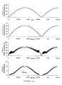
図6、7、および8は、それぞれ、到来するACライン電圧入力が110V ACの公称値であるとき、到来するACライン電圧入力が公称値より10%高いとき、および到来するACライン電圧入力が公称値より30%低いときの、図3および4のAC LEDランプ50の動作を示す波形図である。例示的な回路では、グループ57、58、59、60、61、および62内のLEDの数は、それぞれ、1、2、4、8、16、および18である(N=1)。電流センス抵抗器90は、約43.3オームの小さな抵抗を有し、抵抗器90の両端の電圧降下は小さく(たとえば、十分に1ボルト未満)、抵抗器90にわたる電力損失は小さい。LED電力は、(調節後)5ワットであり、この値は、到来するACライン電圧入力の振幅が77V ACから143V ACまで変わっても変化しない。
FIGS. 6, 7 and 8 respectively show that when the incoming AC line voltage input is a nominal value of 110V AC, when the incoming AC line voltage input is 10% higher than the nominal value, and when the incoming AC line voltage input is FIG. 5 is a waveform diagram illustrating the operation of the
「整流された入力(V)(RECTIFIED INPUT(V))」と表示された図6の一番上の波形は、図3における導体80上の整流された信号(入力)の電圧波形を示す。「アクティブLEDカウント(ACTIVE LED COUNT)」と表示された図6の下方向の次の波形は、LEDストリングのLEDのどれだけの数(LEDCOUNT)が、LEDストリング電流を流するようにさせられるかを示す。CLK信号は図6に示されないが、LEDCOUNTは、信号CLKの立上りエッジ時に増加するだけである。図6に示す整流された正弦波波形の一番上などにおいて、整流された入力電圧が徐々に変化するだけである条件では、LEDCOUNTは、整流された入力電圧がより急速に変化するときに比べて、頻度少なく増加する。「アクティブLEDカウント」波形では、ライン電圧が低い時間の間、LEDCOUNTがゼロ(または、トライアック・リセット電流を確保するために非常に小さな値)であることに留意されたい。これらのときに、回路は、先に説明したように、信号RESET97によってリセットされる。「入力電流(mA)(INPUT CURRENT (mA))」と表示された図6の下方向の3番目の波形は、整流された入力電圧が増加しているときの間、一連の鋸歯状波形状を含む。こうしたそれぞれの鋸歯状波形状のよりゆっくりと立上る部分は、整流された入力電圧が一定数のLEDを通して増加するため、LEDストリング電流の増加を示す。電流センス抵抗器90の両端で検知されるLEDストリング電流が、電流センス閾値信号104を超えると、アップ/ダウン比較器103は、アップ/ダウン・カウンタ122を使用可能にし、アップ/ダウン・カウンタ122は、CLKの次の立上りで増分する。この増分は、より多くのLEDを、LEDストリング電流経路に切換え投入し、これは、LEDストリング電流の急峻な減少をもたらす。この急峻な減少は、鋸歯状波形状の急峻な下方向部分によって示される。
The top waveform of FIG. 6 labeled “Rectified Input (V)” shows the voltage waveform of the rectified signal (input) on
整流された入力電圧が減少するときの間に起こる鋸歯状波形状は、整流された入力電圧が増加するときの間に起こる鋸歯状波形状と比較して、反転形状を有する。整流された入力電圧が減少するときの間に起こる反転した鋸歯状波形状は、よりゆっくりと減少する入力電流部分を含む。この減少する入力電流部分は、減少する整流されたライン電圧が、LEDストリング内の一定数のLEDにわたって降下するからである。電流が、低くなるため、電流センス閾値信号104を下回ると、アップ/ダウン比較器103は、アップ/ダウン・カウンタ122を使用可能にする。アップ/ダウン・カウンタ122は、減分し、それにより、LED電流が通過するLEDストリング内のLEDの数を減少させる。結果として、LEDストリング電流は、ほぼ垂直に立上る。この急峻な増加は、反転した鋸歯状波形状の端部の急峻な上方向部分によって示される。
The sawtooth waveform that occurs while the rectified input voltage decreases has an inverted shape compared to the sawtooth waveform that occurs while the rectified input voltage increases. The inverted sawtooth waveform that occurs while the rectified input voltage decreases includes a portion of the input current that decreases more slowly. This decreasing input current portion is because the decreasing rectified line voltage drops across a certain number of LEDs in the LED string. The up / down
図9は、80V ACから140V ACの範囲の電圧の入力ACラインの場合の、図3および4のAC LEDランプ50のLED電力、ランプ入力電力、効率、入力電力の力率を示す波形図のセットである。光出力(LED電力)が、広い範囲の電圧のラインについて十分に調節されていることが見てわかる。効率は、通常、(整流器51による1%の効率損失を含む)96%であり、スイッチング変換トポロジまたは電流制限抵抗器トポロジより優れていることも見てわかる。最後に、力率が0.97にあるか又はその近傍の値にあることが見てわかる。
FIG. 9 is a waveform diagram showing the LED power, lamp input power, efficiency, and input power power factor of the
図10は、AC LEDランプ50のフリッカ防止動作を示す波形図のセットである。この機構が使用可能にされると、LED電流は、整流されたライン電圧のピークよりわずかに低いOVPレベルでターンオフされる。たとえば、整流された入力電圧がそのピークにあるとき、第3の波形によって示されるように、LED電流がゼロまたはほぼゼロである期間が存在することに留意されたい。さらに、整流された入力電圧がその最小値にあるときの間にも微量のLED電流が流れる。組み合わせると、結果全体として、端子53および54上のAC入力が60Hzであっても、240HzのLED光変調周波数になる。
FIG. 10 is a set of waveform diagrams showing the flicker prevention operation of the
別の実施形態では、LED電流は、ほぼゼロに減少させるのではなく、光強度の2つの別々にのピークを生成するために、有意の量だけ減少させる。一態様では、レギュレータIC409は、サイクル期間の12%未満の継続時間の間、変化する入力の電流瞬時値の半分を超える分、LED電流を減少させる。たとえば、低減されたLED電流の継続時間は、整流器51で受ける60Hz交流入力の各8.33ミリ秒サイクル中で0.7ミリ秒〜0.9ミリ秒の間である。
In another embodiment, rather than reducing the LED current to approximately zero, it is decreased by a significant amount to produce two separate peaks of light intensity. In one aspect, the
図11は、例示的なLEDランプ・モジュール200の略平面図である。モジュール200は、金属コア・プリント回路板201などのプリント回路板または基板、図3および4の集積回路52、光学レンズ202、およびLEDのダイ203を含む。49または98個の各LEDが、ダイ203上に実現される。図上の空間的制限のため、図11の図において全てのLEDを識別するために、参照番号が設けられていないが、図11に示すLEDは、図4に示されるのと同じLEDである。光学レンズ202は、放出された光を所望の方向に向ける。金属コア・プリント回路板201は、熱伝導性があり、かつ、電気的に絶縁される。図11の実施形態では、集積回路52は、半導体ダイであり、半導体ダイは、示すように、ボンド・ワイヤによって、プリント回路板201およびダイ203にワイヤボンディングされる。あるいは、集積回路52は、プリント回路板201に直接ボンディングされるように、チップスケール・マイクロバンプを備え得る。VIN(整流器51からの整流された入力)を受けるパッド204が設けられる。パッド204は、導体205およびボンド・パッドおよびボンド・ワイヤによって、集積回路52のL5端子81に結合される。接地(整流器51からのVSS)に結合するパッド206が設けられる。パッド206は、導体207およびボンド・パッドおよびボンド・ワイヤによって、集積回路52のVSS端子82に結合される。ライン・イン電圧入力が110V ACである実施形態では、ダイ203の図上の各LEDシンボルは1つのLEDを示し、一方、ライン・イン電圧入力が220V ACである実施形態の場合、各LEDシンボルは、直列接続の2つのLEDを示す。この実施形態のLEDは全て、単一ダイ上に配設されているが、そうでなくても良い。各LEDは、相互に対して、また、レンズ203に対して図示のように方向づけされる。
FIG. 11 is a schematic plan view of an exemplary
図12は、AC LEDランプ300の略図である。ランプ300は、入力端子301および302、1つのダイオード整流器ブリッジ303、および図11に示したタイプの複数のモジュール304〜306を含む。モジュールは、示すように、並列に接続される。並列に配置し得るモジュールの数についての制限は存在しない。この配置構成は、互いから異なる距離に配置される複数のランプ・モジュールを必要とする複数の異なるタイプの照明器具について使用されうる。この柔軟性がある配置構成は、異なる数のLEDモジュールを必要とする複数の異なるタイプの照明器具について使用されうる。モジュール式設計は、ランプ製造業者のための在庫を減らす点で有利である。ランプ製造業者は、1つのタイプのLEDランプ・モジュールを在庫する必要があるだけであるが、製造業者は、多くの異なるタイプの照明器具を作り得る。
FIG. 12 is a schematic diagram of an
図13は、AC LEDランプ400の第2の実施形態の図である。この実施形態では、電力スイッチの数は、図3および4の実施形態と比較して、減少する。LEDグループ401、402、403、および404だけが切換り、残りのLEDは、LEDグループ405を形成し、このグループ405は、常に、LEDストリング電流経路内にある。この実施形態は、単純な設計を有するが、効率が少し低い。110V ACライン・イン入力の実施形態では、LEDグループ401、402、403、および404は、それぞれ、2、4、8、および16のLEDを有し(N=2に相当する)、一方、LEDグループ405は、約18のLEDを有する(M=18に相当する)。220V ACライン・イン入力の実施形態では、LEDグループ401、402、403、および404は、それぞれ、4、8、16、および32のLEDを有し(N=4に相当する)、一方、LEDグループ405は、約36のLEDを有する(M=36に相当する)。フリッカを低減するために、谷充填キャパシタ406が設けられる。キャパシタ406は、ノード407と、集積回路409のCAP端子408との間に接続される。この谷充填キャパシタ406は、ノード407上の整流されたライン電圧の電圧ピークまで充電され、その後の瞬時ライン電圧の減少の間、瞬時ライン電圧が谷電圧閾値未満に降下する時点まで、整流されたライン電圧から切離され、当該の時点では、谷充填キャパシタ406は、CAP端子408を通してLEDストリングに再接続される。結果として、瞬時ライン電圧がその谷にあるときの間、ノード407上に補助電圧が生じる。
FIG. 13 is a diagram of a second embodiment of an
図14は、図13の集積回路409のより詳細な図である。集積回路409は、LEDグループ401、402、403、および404を短絡除外する電力スイッチ410、411、412、および413をそれぞれ備える。電力スイッチは、内部給電回路416から受ける内部供給電圧VCCを使用して、コントローラ414およびデコーダ415によって制御される。コントローラ414は、図4のコントローラ92と同様に動作する。デコーダ415は、コントローラ414から受けるLEDCOUNT信号を、ゲート駆動用信号へ変換する、すなわち、電流を所望の数のLEDを通して流すようにする、電力スイッチ410〜413用の適切なゲート駆動用信号へと変換する。電力スイッチ410〜413に加えて、保護スイッチ417は、通常動作中に、LEDストリング電流を許容するために、CSN端子418をVSS端子419に接続する。谷充填スイッチ420が使用されて、整流されたピーク・ライン電圧への谷充填キャパシタ406の充電を制御し、また、瞬時ライン電圧が低い適切なときに、谷充填キャパシタ406の放電を制御する。谷充填スイッチ420は、選択された瞬時ライン電圧が増加すると、オンにラッチされ、ピーク電圧でオフにラッチされる。谷充填スイッチ420は、LEDCOUNT信号が所定の値まで降下したときに、再びオンにラッチされる。この谷充填技法を使用することによって、ランプの光出力は、ライン周波数の4倍(50Hzライン周波数の場合200Hzおよび60Hzライン周波数の場合240Hz)でフラッシュし、それにより、動き関連のフリッカ作用を最小にする。
FIG. 14 is a more detailed diagram of the
図15は、図13および14の回路要素を利用するAC LEDランプ構造500の図である。2×8LEDの4つのグループ501〜504は、中心の1つのグループの1×16LED506と組み合わせて、プリント回路板505の周辺で使用される。2×8LEDの各グループは、2つのストリングとして接続される16の発光ダイオードの結合部を含み、各ストリングは、直列接続の8つの結合部を含み、各グループを、直列接続の8つのLEDの1つのストリングと挙動が等価となるようにさせる。全てのこれらのLEDは、光を収束する光学レンズの下に配置される。円507〜511はレンズを示す。1×16LEDのグループ506は、全てが、光を収束する光学レンズ511の下に配置された、直列接続の16のLEDを有する。2×8LEDのグループは、図14のLEDグループ405(直列接続の全部で18のLEDのうちの16のLED)および図14のLEDグループ404(直列接続の16のLED)を構成する。1×16LEDのグループ506は、2、4、および8のLEDの2値セグメントに分割される。1×16LEDのグループ506は、それぞれ、LEDグループ405(2つの残りのLED)、LEDグループ401、LEDグループ402、およびLEDグループ403を構成する。LEDグループ401、402、および403内のLEDは、瞬時ライン電圧の遷移のために、約50%デューティ・サイクルで動作するため、中心の1×16LEDのグループ506の電力消費は、LEDの周辺グループの電力消費と同じ程度である。したがって、全てのLEDのグループ(501〜504および506)は、同じかまたは同様なLEDダイから作られうる。集積回路409、電流センス抵抗器421、整流器422、谷充填キャパシタ406は、それぞれの参照番号によって図15で識別される。図13の入力電力端子423および424は、同じ参照番号によって図16で識別される。図13の導体425〜431は、同じ参照番号によって図15で識別される。集積回路409は、パッケージングされた集積回路、チップスケール・マイクロバンプ付きシリコン・ダイ、または、プリント回路板505にワイヤボンディングされたシリコン・ダイであってよい。
FIG. 15 is a diagram of an AC
なお別の実施形態では、LEDグループは、同じ数のLEDを有し、電力スイッチは、全てのLEDグループが同じ平均光出力を有するように、互いに対称に動作する。これは、LEDが、LEDごとに観測可能な輝度変化をすることなく、照明器具内の異なる位置に配置されることを可能にする。LEDグループの数は、2〜16までであることができ、4、5、6が好ましい数であり、単純さと効率との間の均衡を提供する。 In yet another embodiment, the LED groups have the same number of LEDs and the power switches operate symmetrically with each other so that all LED groups have the same average light output. This allows the LEDs to be placed at different locations within the luminaire without observable brightness changes from LED to LED. The number of LED groups can be from 2 to 16, with 4, 5, 6 being preferred numbers, providing a balance between simplicity and efficiency.
図16は、第3の実施形態の図である。AC LEDランプ600は、電力入力端子601および602、整流器603、集積回路604、およびLEDの5つのグループ605〜609を含む。集積回路604内には、LEDの5つの対応するグループ605〜609を制御する5つの電力スイッチ610〜614が存在する。LEDの各グループは、同じNの数のLEDを有し、ここで、Nは整数である。この実施形態では、コントローラ615は、図5のコントローラ92と同様な方法で動作する。一方、デコーダ616はまた、LEDの全てのグループ間の電力消費を均一にするように処理する。
FIG. 16 is a diagram of the third embodiment. The
図17は、図16のデコーダ616のより詳細な図である。ルックアップ読取り専用メモリ(ROM)回路617は、入力として、3ビットLEDCOUNT値ならびに3ビットSCATTER信号618を受ける。これらの6ビットから、ルックアップROM回路617は、レベル・シフト回路619によってレベル・シフトされる5ビット・コードNG0〜NG4を出力する。5ビット・コードによって指令される(direct)ように、レベル・シフト回路619は、電力スイッチ605〜609を駆動する。SCATTER信号618は、CLK信号によってクロック駆動されるカウンタ620によって生成される。カウンタ620は、ライン・イン電圧の各半サイクルの始めにおいて、信号RESETによって第2カウンタ621の状態をロードされる。両方のカウンタ620および621は、4の値に達した後、ゼロに戻るように循環される。カウンタ621はまた、信号RESETによってクロック駆動される。結果として、SCATTER信号618は、0から4の範囲の3ビット値を有し、この値は、短い各CLK期間後に増分され、5つの順次ライン・イン電圧半サイクルのそれぞれについて異なる開始値を有する。
FIG. 17 is a more detailed diagram of the
図18は、ルックアップROM617の動作を示す表である。到来する各LEDCOUNT値について、デコーダ616は、正しい数のLEDがアクティブになるように制御するが、どの特定のグループのLEDがアクティブにさせられるかについての実際の決定は、各CLK期間について変わる。したがって、信号CLKの複数のサイクルにわたって、LEDの各グループがオンである平均デューティ・サイクルは同じである。デューティ・サイクルに関するこのLEDの最大の一致を確保するために、5つの順次ライン・イン電圧半サイクルに対して、LEDの異なるグループ間のデューティ・サイクルの小さな不一致がなくなるように、カウンタ621は、5つの順次ライン・イン電圧半サイクルのそれぞれについて、異なる開始カウントを提供する。同様に、最良一致作用の場合、LED電流制限VILIMは、LEDが、(N・VF)より高い整流された任意の瞬時ライン電圧において本質的に一定電流レベルで動作するように設定される。この動作モードでは、保護スイッチ622は、通常動作において、定電流源として動作し、コントローラ615は、アップ/ダウン・カウントのために、保護スイッチ622の両端の電圧を検出する。フリッカ防止のために、保護スイッチ622は、LEDストリングの実効動作周波数を2倍にするために、整流された瞬時ライン電圧のピークでターンオフする。
FIG. 18 is a table showing the operation of the
図19は、AC LEDランプ700の図である。ランプ700は、図16の集積回路604を含む。このランプでは、LEDの5つのグループが使用される。各グループは、同じ数のLEDを有する。110V ACライン・イン用の場合、LEDの各グループは、直列に結合された約10のLEDダイを有する(N=10)。220V ACライン・イン用の場合、LEDの各グループは、直列接続の約20のLEDダイを有する(N=20)。12V ACライン・イン用の場合、LED電力が5ワットである用途において、LEDの各グループは、単一の1ワットLEDを有する。24V ACライン・イン用の場合、LED電力が5ワットである用途において、LEDの各グループは、全部で1ワットになるために、直列に結合された2つのLEDダイを有する。集積回路604、電流センス抵抗器623、および整流器603はまた、ランプ700内に設置される。集積回路604は、パッケージングされた集積回路、チップスケール・マイクロバンプ付きシリコン・ダイ、または、プリント回路板701にワイヤボンディングされたシリコン・ダイであってよい。円シンボル702〜706はレンズを示す。図16の導体624〜631は、同じ参照番号によって図19で識別される。
FIG. 19 is a diagram of an
図20は、新規な方法707のフローチャートである。第1ステップ(ステップ708)にて、ACライン・イン電力入力は、変化する電圧の入力が第1のノードと第2のノードとの間に生じるように、受けられる。方法707の一実施形態では、ACライン・イン電力入力は、図3および4のAC LEDランプ50の端子53と54で受けられる110V AC 60Hz入力である。対応する変化する電圧の入力(たとえば、ACライン・イン入力の全波整流されたもの)は、LEDストリングの第1の端部55とLEDストリングの第2の端部56との間に生じる。
FIG. 20 is a flowchart of the
第2のステップ(ステップ709)では、(第1のノードから第2のノードへ)通電することを許容されるLEDストリングのLEDの数は、変化する電圧入力の電圧振幅が増加すると数が増加するように、また、変化する電圧入力の電圧振幅が減少すると数が減少するように制御される。数は、電圧振幅が変化するにつれて、多くの(たとえば、少なくとも2つの)異なる離散的な値を有する。一実施形態では、変化する電圧入力は、図6で、「整流された入力(V)」として、一番上の波形で示される。電流が流れることを許容されるLEDの数は、図6で「アクティブLEDカウント」と表示される波形に示すように増減する。 In the second step (step 709), the number of LEDs in the LED string that are allowed to energize (from the first node to the second node) increases as the voltage amplitude of the changing voltage input increases. In addition, the number is controlled to decrease as the voltage amplitude of the changing voltage input decreases. The number has many (eg, at least two) different discrete values as the voltage amplitude changes. In one embodiment, the changing voltage input is shown in the top waveform as “rectified input (V)” in FIG. The number of LEDs allowed to pass current increases or decreases as shown in the waveform labeled “Active LED Count” in FIG.
図3および4の第1の実施形態では、電力スイッチは、ダイ面積を最適にするようなサイズにされる。典型的な作製プロセスでは、MOSFETの固有抵抗は、絶縁破壊電圧にほぼ逆比例する。所与のダイ面積について、オンであるときの電力スイッチの抵抗は、オフであるときの、その定格絶縁破壊電圧にほぼ比例して増加する。したがって、電力スイッチが、切換えられるLEDのグループにおける全LED順方向電圧降下より高い絶縁破壊電圧を有する必要があるため、より多くのLEDを駆動する電力スイッチについてより高いオン抵抗を可能にすることが最善である。保護スイッチ89は、整流されたピーク電圧を維持することができる必要がある。5ワット110V AC用途についての図3および4の第1の実施形態では、保護スイッチ89は、48オームの抵抗を有し、定格を200Vにすることができ、電力スイッチ88および87は、48オームの抵抗を有し、定格を80Vにすることができ、電力スイッチ86は、24オームの抵抗を有し、定格を40Vにすることができ、電力スイッチ85は、12オームの抵抗を有し、定格を20Vにすることができ、電力スイッチ84は、6オームの抵抗を有し、定格を10Vにすることができ、電力スイッチ83は、3オームの抵抗を有し、定格を5Vにすることができる。5ワット220V AC用途についての図3および4の第1の実施形態では、保護スイッチ89は、96オームの抵抗を有し、定格を400Vにすることができ、電力スイッチ88および87は、96オームの抵抗を有し、定格を160Vにすることができ、電力スイッチ86は、48オームの抵抗を有し、定格を80Vにすることができ、電力スイッチ85は、24オームの抵抗を有し、定格を40Vにすることができ、電力スイッチ84は、12オームの抵抗を有し、定格を20Vにすることができ、電力スイッチ83は、6オームの抵抗を有し、定格を10Vにすることができる。
In the first embodiment of FIGS. 3 and 4, the power switch is sized to optimize die area. In a typical fabrication process, the MOSFET resistivity is approximately inversely proportional to the breakdown voltage. For a given die area, the resistance of the power switch when it is on increases approximately in proportion to its rated breakdown voltage when it is off. Thus, because the power switch needs to have a breakdown voltage that is higher than the total LED forward voltage drop in the group of LEDs to be switched, it can allow higher on-resistance for power switches that drive more LEDs. Is the best. The
図16の第3の実施形態では、電力スイッチは、全て同じサイズである。5ワット12V AC用途の場合、電力スイッチは、オンであるとき、約1/2オームの抵抗を有し、それぞれ、定格を5ボルトにすることができる。5ワット24V AC用途の場合、電力スイッチは、オンであるとき、約1オームの抵抗を有し、それぞれ、定格を10ボルトにすることができる。5ワット110V AC用途の場合、電力スイッチは、オンであるとき、約5オームの抵抗を有し、それぞれ、定格を50ボルトにすることができる。5ワット220V AC用途の場合、電力スイッチは、オンであるとき、約10オームの抵抗を有し、それぞれ、定格を100ボルトにすることができる。 In the third embodiment of FIG. 16, the power switches are all the same size. For 5 watt 12V AC applications, the power switch, when turned on, has a resistance of about 1/2 ohm and can each be rated at 5 volts. For 5 watt 24V AC applications, the power switch, when on, has a resistance of about 1 ohm and can each be rated at 10 volts. For a 5 watt 110V AC application, the power switch, when on, has a resistance of about 5 ohms, each of which can be rated at 50 volts. For a 5 watt 220V AC application, the power switch, when on, has a resistance of about 10 ohms and can each be rated at 100 volts.
上述した実施形態は、固体AC LEDランプを作るのに、比較的少数のコンポーネントだけが必要とされる点で有利である。結果として、AC LEDランプは、優れた信頼性および長い平均故障間隔を有する。さらに、第1の実施形態および第3の実施形態のAC LEDランプは、信頼性を低下させる可能性がある電解キャパシタを全く含む必要がない。高い効率を達成することによって、エネルギーがほとんど浪費されない。電磁干渉(EMI)問題は、多くのAC−DC変換器LEDランプと比較して最小になる。その理由は、上述したAC LEDランプの実施形態が、高周波電力スイッチングを全く含まないからである。 The embodiments described above are advantageous in that only a relatively small number of components are required to make a solid state AC LED lamp. As a result, AC LED lamps have excellent reliability and long mean time between failures. Furthermore, the AC LED lamps of the first and third embodiments need not include any electrolytic capacitors that can reduce reliability. By achieving high efficiency, little energy is wasted. Electromagnetic interference (EMI) problems are minimized compared to many AC-DC converter LED lamps. The reason is that the AC LED lamp embodiment described above does not include any high frequency power switching.
電力スイッチを制御するために、特定用途向け回路要素の制御回路を使用することなしに、別の実施形態の制御機能が、電力スイッチを制御する、柔軟性がありかつプログラマブルなマイクロコントローラによって実施され得る。電力スイッチ、電流センス抵抗器、および保護スイッチは、マイクロコントローラの残りと共に、ある集積回路上で実現されてもよい。あるいは、電力スイッチ、電流センス抵抗器、および保護スイッチは、マイクロコントローラ集積回路の外部に設けられてもよい。マイクロコントローラは、整流されたライン・イン電圧入力のゼロ位相のときを検出するのに使用されるゼロ交差検出比較器を有する。マイクロコントローラはまた、LEDストリングにわたる電圧降下の大きさを検出し、また、電流センス抵抗器の両端の電圧降下の大きさを検出するのに使用される、アナログ−デジタル変換器および関連する入力マルチプレクサを有する。マイクロコントローラのタイマは、検出されるイベントおよび条件の発生を計時するのに使用され、また、マイクロコントローラのある出力を計時し制御するのに使用される。マイクロコントローラの入力/出力(I/O)端子は、スイッチが外部にある場合、電力スイッチのゲートを駆動し制御するのに使用されるか、または、電力スイッチが内部にある場合、LEDストリングの相互接続ノードに結合される。マイクロコントローラは、外部の電力MOSFETのゲートを駆動する特別なゲート駆動回路要素を備えてもよい。マイクロコントローラは、これらの入力回路および出力回路および他の資源を使用して、図4の集積回路52に関連して上述した機能を実施するようにプログラムされる。
Without using an application specific circuit element control circuit to control the power switch, the control function of another embodiment is implemented by a flexible and programmable microcontroller that controls the power switch. obtain. The power switch, current sense resistor, and protection switch may be implemented on an integrated circuit along with the rest of the microcontroller. Alternatively, the power switch, current sense resistor, and protection switch may be provided external to the microcontroller integrated circuit. The microcontroller has a zero-crossing detection comparator that is used to detect when the rectified line-in voltage input is at zero phase. The microcontroller also detects the magnitude of the voltage drop across the LED string, and the analog-to-digital converter and associated input multiplexer used to detect the magnitude of the voltage drop across the current sense resistor. Have The microcontroller timer is used to time the occurrence of detected events and conditions, and is used to time and control certain outputs of the microcontroller. The input / output (I / O) terminal of the microcontroller is used to drive and control the gate of the power switch when the switch is external, or of the LED string when the power switch is internal Coupled to the interconnect node. The microcontroller may include special gate drive circuitry that drives the gate of the external power MOSFET. The microcontroller is programmed to perform the functions described above with respect to the
図21は、AC LEDランプの第2の実施形態のフリッカ防止動作モードを示す図14の変更例の図である。図21は、全波整流器422が、第1のノード710および接地ノード711に結合されることを示す。接地ノード711は、接地端子419に結合される。LED電流は、直列接続されたLEDのストリング712を通して、第1のノード710から第2のノード713へ流れる。谷充填キャパシタ406は、第1のノード710および第3のノード714に結合される。キャパシタ端子408は、第3のノード714ならびに谷充填スイッチ420に結合される。スイッチ端子715は、第2のノード713に結合される。谷充填スイッチ420は、キャパシタ端子408をVSS端子419に選択的に結合する。
FIG. 21 is a diagram of a modification of FIG. 14 illustrating the flicker prevention operation mode of the second embodiment of the AC LED lamp. FIG. 21 shows that a
フリッカを低減するために、整流器422による第1のノード710上の変化する電圧の入力からのエネルギーは、変化する電圧の入力の電圧振幅が増加するにつれて、谷充填キャパシタ406に蓄積される。別の実施形態では、変化する電圧の入力からのエネルギーは、インダクタなどのキャパシタ以外の受動コンポーネントに蓄積される。その後、蓄積されたエネルギーは、変化する電圧の入力の電圧振幅が、谷電圧閾値より降下すると、谷充填キャパシタ406から放出される。谷充填キャパシタ406から放出されるエネルギーによって生成される光のバーストは、その周波数が、整流器422によって出力される変化する電圧入力の周波数の2倍であるLED電流入力を生成する。整流器422が、整流された120Hzの変化する電圧入力に変換する60Hz入力の場合、たとえば、LEDストリング712によって受けれるLED電流入力は、240Hzの周波数を有する。そのため、LEDストリング712は、240回/秒で光強度のピークを放出する。60Hz入力の各サイクルについて生成される光強度の4つのピークは、必ずしも周期的または等間隔ではない。それでも、LEDランプによって出力される光変調周波数(たとえ不均一であっても)は、240Hzであり、移動物体を観測するときでさえも、フリッカがそれについて知覚される周波数を十分に超えている。
In order to reduce flicker, energy from the changing voltage input on the first node 710 by the
図22は、谷充填キャパシタ406がフリッカ防止モードで使用されるときの、図21のAC LEDランプの動作を示す波形図である。一番上の波形716は、LEDストリング712にわたる電圧を示す。谷充填スイッチ420は、整流器422で受電される交流入力の第1の部分717においては、閉路して、キャパシタ端子408およびVSS端子419を結合させて谷充填キャパシタ406を充電させる。谷充填キャパシタ406は、開始期間718中に放電し、終了期間719中に充電される。谷充填スイッチ420は、交流入力の第2の部分720中に開路し、それにより、谷充填キャパシタ406上の電荷を維持し、その電荷は、交流入力が谷電圧閾値721より下がる電圧を有するときに、第1のノード710上の電圧を上げるのに後で使用される。
FIG. 22 is a waveform diagram showing the operation of the AC LED lamp of FIG. 21 when the
第1のノード710上の電圧が谷電圧閾値721より下がると、レギュレータIC409は、谷充填スイッチ420を閉路することによって、谷充填キャパシタ406を第1のノード710に結合する。谷充填キャパシタ406に蓄積された電荷は、その後、LEDストリング712にわたる電圧を急速に増加させ、光強度のピークを生成する。アクティブLEDカウント722の曲線は、第1のノード710上の充電電圧に追従するために、レギュレータIC409が、さらなるLEDをLEDストリング712上にどのように結合させるかを示す。レギュレータIC409は、アクティブLEDカウントに追従することによって、第1のノード710上の電圧が谷電圧閾値721より下がったときを決定する。
When the voltage on the first node 710 falls below the valley voltage threshold 721, the
LEDカウントはまた、谷充填キャパシタ406を切離すときを決定するのに使用されうる。一部の実施形態では、谷充填キャパシタ406は、変化する電圧の入力の正確にピーク振幅において、変化する電圧の入力から切り離さない。代わりに、谷充填スイッチ420が、変化する電圧入力から谷充填キャパシタ406を切り離すように開路するのは、変化する電圧入力の電圧振幅がピーク振幅の少なくとも90%となる任意の所定の時刻である。アクティブLEDカウント信号722は、第1のノード710上の電圧に追従するため、谷充填スイッチ420が開放するときを設定するのに使用されうる。
The LED count can also be used to determine when to disconnect the
図4のレギュレータIC52と同様に、レギュレータIC409は、LEDストリング712にわたる、変化する電圧について適切なLEDの数を決定するコントローラ414を組込む。コントローラ414はまた、トライアック調光器からの位相カット角の検出に基づいてLED電流を調整する。標準的なトライアック調光器回路では、トライアックは、照明負荷に供給される全電力を低減するために、到来するAC入力の部分または整流されたライン入力の部分を開回路にしてもよい。レギュレータIC409を、標準的なトライアック調光器を含む用途で動作可能にするために、端子715と端子418との間の電圧を調節するための電圧閾値は、検出される調光器位相カット角によって調整されるため、位相カットが大きくなればなるほど、平均LED電力が小さくなる。
Similar to
図22の実施形態では、LEDストリング712の平均電力は5ワットである。谷充填キャパシタ406は、1.5μFのキャパシタンスを有し、谷電圧閾値は、82ボルトである。整流器422によって出力される変化する電圧入力の電流波形723は、この実施態様では、比較的一定のままであるため、LEDストリング712によって放出される光の強度はまた、比較的一定のままである。この実施態様は、高い電力力率を達成することに比べて、少ない光変動が好ましい用途において適切である。高い力率を維持することがより重要である場合、レギュレータIC409は、瞬時電流を、LEDカウントに比例するように調節する。この実施態様では、力率は、0.74であるように計算される。変化する電圧信号の電流波形723は、第1のノード710上の電圧が、谷電圧閾値721を超えて上がり始めるため、谷充填キャパシタ406を充電することによって、大きな電流を有する前縁を有する。
In the embodiment of FIG. 22, the average power of the
波形724はLED電力である。整流器422上で受けられる60Hz交流入力の全ての8.33ミリ秒サイクルについて、波形724は2つのピークを有する。ピークは等間隔ではないが、波形724は、240Hzの実効周波数を有する。この実施態様では、LED電力の変動は、平均LED電力から+/−40%未満に減少する。
ある特定の実施形態が、教示のために上述されたが、本明細書の教示は、一般的な適用可能性を有し、上述した特定の実施形態に限定されない。LEDのグループ内のLEDの数は、示した実施形態で述べた数と異なりうる。各LEDは、任意の数のLEDを、並列にかつ同じ方向に結合することによって作られることができ、1つのLEDに対する参照も、並列なLEDの任意のこうした結合を指す。各LEDグループまたはセクションについて、直列接続のLEDの数は、電流が印加されると、匹敵する全順方向電圧降下をもたらすLEDの並列および直列ネットワークの任意の方法を示すのに使用される。さらに、全体のLEDストリング内の異なるLEDのグループの接続の順序は、異なる順序でありうる。LEDストリングは、直列接続されていないセクションを備えてもよい。LEDストリングは、LEDでないデバイスを備えてもよい。センス抵抗器は、集積回路の内部であっても、外部であってもよい。電力スイッチは、Nチャネル電界効果トランジスタ(NFET)、Pチャネル電界効果トランジスタ(PFET)、または別の適したタイプのスイッチでありうる。キャパシタ、過渡的抑止器、電流制限抵抗器、およびヒューズなどのさらなる外部コンポーネントが、性能を改善するために付加されてもよい。整流器ダイオード・ブリッジは、一部の実施形態では、集積回路内に組み込まれてもよく、特に、12V ACおよび24V ACライン・イン用などの低電圧用途の場合、電圧降下を低減するために、アクティブMOSFETと置換えられてもよい。したがって、述べた実施形態の種々の特徴についての種々の変更、適応、および組合せが、特許請求の範囲で述べられる本発明の範囲から逸脱することなく実施されうる。 Although certain specific embodiments have been described above for teaching purposes, the teachings herein have general applicability and are not limited to the specific embodiments described above. The number of LEDs in the group of LEDs may differ from the number described in the illustrated embodiment. Each LED can be made by combining any number of LEDs in parallel and in the same direction, and a reference to one LED also refers to any such combination of LEDs in parallel. For each LED group or section, the number of LEDs connected in series is used to indicate any method of parallel and series network of LEDs that results in a comparable total forward voltage drop when current is applied. Further, the order of connection of different LED groups within the entire LED string may be different. The LED string may comprise sections that are not connected in series. The LED string may comprise devices that are not LEDs. The sense resistor may be internal or external to the integrated circuit. The power switch can be an N-channel field effect transistor (NFET), a P-channel field effect transistor (PFET), or another suitable type of switch. Additional external components such as capacitors, transient arresters, current limiting resistors, and fuses may be added to improve performance. The rectifier diode bridge may be incorporated in an integrated circuit in some embodiments, particularly for low voltage applications such as for 12V AC and 24V AC line-in to reduce voltage drop. It may be replaced with an active MOSFET. Accordingly, various modifications, adaptations, and combinations of the various features of the described embodiments can be practiced without departing from the scope of the invention as set forth in the claims.
52、409、604 LEDランプ・レギュレータIC;
55 LEDストリングの第1の端部; 56 LEDストリングの第2の端部;
57、401、605、606、607、608、609 LEDグループ(N個のLED);
58、402 LEDグループ(2N個);
59、403 LEDグループ(4N個);
60、404 LEDグループ(8N個);
61 LEDグループ(16N個);
62 LEDグループ(P個);
91、416 内部給電; 92、414、615 コントローラ;
93、415、616 デコーダ;
94 6ビット・デジタルLEDCOUNT信号;
96 パワー・オン・リセット回路; 97 リセット信号; 98 アップ信号;
100 クロック発生器; 101 位相制御;
102 アップ/ダウン・カウンタ; 103 アップ/ダウン比較器;
104 電流センス閾値信号; 109、112 スケーラ; 111 エラー信号;
113 保護ゲート信号; 117 過温度保護回路;
200、304、305、306 LEDランプ・モジュール;
405 LEDグループ(MのLED); 406 谷充填キャパシタ;
408 キャパシタ端子; 419 接地端子; 421 電流センス抵抗器;
617 ルックアップROM; 618 3ビットSCATTER信号;
619 レベル・シフト; 620、621 カウンタ; 710 第1のノード;
711 接地ノード; 712 LEDストリング; 713 第2のノード:
714 第3のノード; 715 スイッチ端子; 717 交流入力の第1の部分;
720 交流入力の第2の部分; 721 谷電圧閾値。
52, 409, 604 LED lamp regulator IC;
55 a first end of the LED string; 56 a second end of the LED string;
57, 401, 605, 606, 607, 608, 609 LED groups (N LEDs);
58, 402 LED groups (2N);
59, 403 LED groups (4N);
60, 404 LED groups (8N);
61 LED groups (16N);
62 LED groups (P);
91, 416 internal power supply; 92, 414, 615 controller;
93, 415, 616 decoder;
94 6-bit digital LEDCOUNT signal;
96 power-on reset circuit; 97 reset signal; 98 up signal;
100 clock generator; 101 phase control;
102 up / down counter; 103 up / down comparator;
104 current sense threshold signal; 109, 112 scaler; 111 error signal;
113 protection gate signal; 117 overtemperature protection circuit;
200, 304, 305, 306 LED lamp module;
405 LED groups (M LEDs); 406 Valley filled capacitors;
408 capacitor terminal; 419 ground terminal; 421 current sense resistor;
617 Look-up ROM; 618 3-bit SCATTER signal;
619 level shift; 620, 621 counter; 710 first node;
711 Ground node; 712 LED string; 713 Second node:
714 third node; 715 switch terminal; 717 first portion of AC input;
720 second portion of AC input; 721 Valley voltage threshold.
Claims (30)
第1の端子と、
第2の端子と、
前記第1および第2の端子を選択的に結合するように結合される電力スイッチと、
前記集積回路の外部の発光ダイオード(LED)のストリングの電気特性の少なくとも一部に基づいて前記電力スイッチを制御するようになっている制御回路および入力電圧とを備え、第1の時間中、電流は前記電力スイッチを通って流れ、第2の時間中、電流は前記電力スイッチを通って流れず、前記第2の時間中の前記入力電圧は、前記第1の時間中の前記入力電圧より高い集積回路。 An integrated circuit,
A first terminal;
A second terminal;
A power switch coupled to selectively couple the first and second terminals;
A control circuit adapted to control the power switch based on at least part of an electrical characteristic of a string of light emitting diodes (LEDs) external to the integrated circuit and an input voltage, and during the first time, a current Flows through the power switch, during a second time no current flows through the power switch, and the input voltage during the second time is higher than the input voltage during the first time. Integrated circuit.
第2の端子と、
第3の端子と、
前記第1および第2の端子を選択的に結合するように結合される第1の電力スイッチと、
前記第2および第3の端子を選択的に結合するように結合される第2の電力スイッチと、
集積回路の外部の発光ダイオード(LED)のストリングの電気特性に少なくとも部分的に基づいて前記第1および第2のスイッチを制御するようになっている制御回路とを備え、第1の時間中、電流が、前記第1の端子から出て、LEDの前記ストリング上の第1の相互接続ノード上に流れ、第2の時間中、電流は、前記第2の端子から、LEDの前記ストリング上の第2の相互接続ノード上に流れ出る集積回路。 A first terminal;
A second terminal;
A third terminal;
A first power switch coupled to selectively couple the first and second terminals;
A second power switch coupled to selectively couple the second and third terminals;
A control circuit adapted to control the first and second switches based at least in part on an electrical characteristic of a string of light emitting diodes (LEDs) external to the integrated circuit, and during a first time period, A current exits the first terminal and flows on a first interconnect node on the string of LEDs, and during a second time, current flows from the second terminal on the string of LEDs. An integrated circuit that flows out onto the second interconnect node.
集積回路であって、
LEDの前記ストリング上の第1のノードに結合される第1の端子、
LEDの前記ストリング上の第2のノードに結合される第2の端子、
LEDの前記ストリング上の第3のノードに結合される第3の端子、
前記第1および第2の端子を選択的に結合するように結合される第1の電力スイッチ、
前記第2および第3の端子を選択的に結合するように結合される第2の電力スイッチ、 前記第1および第2の電力スイッチを制御する制御回路
を備える、集積回路と、
第1の入力電力ノードと、
第2の入力電力ノードとを備え、電流は、前記第1の入力電力ノードから、前記集積回路によって制御される、ある量のLEDの前記ストリングを通して、前記第2の入力電力ノードへ流れるシステム。 A string of light emitting diodes (LEDs) connected in series;
An integrated circuit,
A first terminal coupled to a first node on the string of LEDs;
A second terminal coupled to a second node on the string of LEDs;
A third terminal coupled to a third node on the string of LEDs;
A first power switch coupled to selectively couple the first and second terminals;
A second power switch coupled to selectively couple the second and third terminals; an integrated circuit comprising a control circuit that controls the first and second power switches;
A first input power node;
A system in which current flows from the first input power node through the string of LEDs controlled by the integrated circuit to the second input power node.
前記AC入力電圧を受ける第2の端子であって、入力電圧の大きさは、前記第1の端子と前記第2の端子との間に存在する、第2の端子と、
前記第1の端子および前記第2の端子に結合する整流器と、
1つまたは複数の発光ダイオード(LED)の第1のストリングと、
1つまたは複数のLEDの第2のストリングとを備え、第1の期間中、第1の電流は、LEDの前記第1のストリングを通って流れるが、LEDの前記第2のストリングを通って電流は流れず、第2の期間中、第2の電流は、LEDの前記第1のストリングとLEDの前記第2のストリングの両方を通って流れ、前記第2の期間中の前記入力電圧の大きさは、前記第1の期間中の前記入力電圧の大きさより大きい装置。 A first terminal that receives an alternating current (AC) input voltage;
A second terminal for receiving the AC input voltage, the magnitude of the input voltage being between the first terminal and the second terminal;
A rectifier coupled to the first terminal and the second terminal;
A first string of one or more light emitting diodes (LEDs);
A second string of one or more LEDs, and during the first period, a first current flows through the first string of LEDs, but through the second string of LEDs. No current flows, and during the second period, a second current flows through both the first string of LEDs and the second string of LEDs, and the input voltage during the second period A device whose magnitude is greater than the magnitude of the input voltage during the first period.
前記整流された瞬時ライン電圧は、その谷にある時に、LEDの前記第1のストリングに補助電圧を提供するキャパシタをさらに備える、請求項14に記載の装置。 The rectifier receives the input voltage and outputs a rectified instantaneous line voltage, the rectified instantaneous line voltage having a valley;
The apparatus of claim 14, further comprising a capacitor that provides an auxiliary voltage to the first string of LEDs when the rectified instantaneous line voltage is in its trough.
1つまたは複数の発光ダイオード(LED)の第1のストリングであって、前記整流された瞬時ライン電圧が、LEDの第1のストリングの入力ノード上に存在する、第1のストリングと、
1つまたは複数のLEDの第2のストリングと、
第1の期間中、LEDの前記第1のストリングを通って第1の電流を流れさせるが、LEDの前記第2のストリングを通って電流を流れさせない制御回路とを備え、第2の期間中、前記制御回路は、LEDの前記第1のストリングとLEDの前記第2のストリングの両方を通って第2の電流を流れさせ、前記整流された瞬時ライン電圧は、前記第1の期間中よりも前記第2の期間中の方が大きい装置。 A rectifier that receives an AC input voltage and outputs a rectified instantaneous line voltage;
A first string of one or more light emitting diodes (LEDs), wherein the rectified instantaneous line voltage is present on an input node of the first string of LEDs;
A second string of one or more LEDs;
A control circuit that causes a first current to flow through the first string of LEDs during the first period, but does not flow current through the second string of LEDs, and during the second period The control circuit causes a second current to flow through both the first string of LEDs and the second string of LEDs, and the rectified instantaneous line voltage is greater than during the first period. A device that is larger during the second period.
前記整流された瞬時ライン電圧は、前記電圧の谷にあるとき、LEDの前記第2のストリングに補助電圧を提供するキャパシタをさらに備える請求項24に記載の装置。 The rectified instantaneous line voltage has a trough,
25. The apparatus of claim 24, further comprising a capacitor that provides an auxiliary voltage to the second string of LEDs when the rectified instantaneous line voltage is in the voltage trough.
LEDの前記第1のストリングと直列に接続された1つまたは複数のLEDの第2のストリングと、
LEDの前記第2のストリングと直列に接続された1つまたは複数のLEDの第3のストリングと、
LEDの前記第2のストリングの入力ノードに結合した第1の端子であって、第1の期間中、LEDの前記第2のストリングを通して電流が流れることを防止するが、第2の期間中および第3の期間中、LEDの前記第2のストリングを通して電流が流れることを可能にするように動作する、第1の端子と、
LEDの前記第3のストリングの入力ノードに結合した第2の端子であって、第1の期間中および第2の期間中、LEDの前記第3のストリングを通して電流が流れることを防止するが、第3の期間中、LEDの前記第3のストリングを通して電流が流れることを可能にするように動作し、LEDの前記第1のストリング、LEDの前記第2のストリングおよびLEDの前記第3のストリングは、異なる数のLEDを有し、LEDの前記第1のストリング内のLEDはそれぞれ、白色LEDである装置。 A first string of one or more light emitting diodes (LEDs), wherein a rectified instantaneous line voltage is present on an input node of the first string of LEDs;
A second string of one or more LEDs connected in series with the first string of LEDs;
A third string of one or more LEDs connected in series with the second string of LEDs;
A first terminal coupled to an input node of the second string of LEDs, preventing current from flowing through the second string of LEDs during the first period, but during the second period and A first terminal that operates to allow current to flow through the second string of LEDs during a third period;
A second terminal coupled to an input node of the third string of LEDs, preventing current from flowing through the third string of LEDs during a first period and a second period; During a third period, the first string of LEDs, the second string of LEDs, and the third string of LEDs operate to allow current to flow through the third string of LEDs. Has a different number of LEDs, each LED in the first string of LEDs being a white LED.
Applications Claiming Priority (4)
| Application Number | Priority Date | Filing Date | Title |
|---|---|---|---|
| US12/661,603 US8299724B2 (en) | 2010-03-19 | 2010-03-19 | AC LED lamp involving an LED string having separately shortable sections |
| US12/661,603 | 2010-03-19 | ||
| US12/799,953 US8456095B2 (en) | 2010-03-19 | 2010-05-04 | Reduced flicker AC LED lamp with separately shortable sections of an LED string |
| US12/799,953 | 2010-05-04 |
Publications (2)
| Publication Number | Publication Date |
|---|---|
| JP2011198739A true JP2011198739A (en) | 2011-10-06 |
| JP5450340B2 JP5450340B2 (en) | 2014-03-26 |
Family
ID=44585478
Family Applications (1)
| Application Number | Title | Priority Date | Filing Date |
|---|---|---|---|
| JP2010229359A Expired - Fee Related JP5450340B2 (en) | 2010-03-19 | 2010-10-12 | Flicker-reduced ACLED lamp with separately shortable sections of LED string |
Country Status (3)
| Country | Link |
|---|---|
| US (2) | US8456095B2 (en) |
| JP (1) | JP5450340B2 (en) |
| DE (1) | DE102010040266A1 (en) |
Cited By (10)
| Publication number | Priority date | Publication date | Assignee | Title |
|---|---|---|---|---|
| WO2014010889A1 (en) * | 2012-07-09 | 2014-01-16 | 서울반도체 주식회사 | Light-emitting diode lighting apparatus |
| JP2014039004A (en) * | 2012-08-10 | 2014-02-27 | Macroblock Inc | Led driving device |
| JP2014154881A (en) * | 2013-02-05 | 2014-08-25 | Lg Innotek Co Ltd | Light emitting module |
| KR101456688B1 (en) * | 2012-11-28 | 2014-10-31 | 아날로그 인테그레이숀즈 코포레이션 | Ac driven lighting systems capable of avoiding dark zone |
| US9084320B2 (en) | 2013-06-03 | 2015-07-14 | Posco Led Company Ltd. | LED luminaire having high power LED drive circuit |
| US9374864B2 (en) | 2014-07-24 | 2016-06-21 | Panasonic Intellectual Property Management Co., Ltd. | Lighting device and light fixture |
| KR101995256B1 (en) * | 2018-12-05 | 2019-07-02 | 영남엘이디 주식회사 | The dimming methods of led lamps to minimize flicker for the full color led lighting |
| KR101995254B1 (en) * | 2018-12-05 | 2019-07-02 | 주식회사 테크엔 | The dimming apparatus of led lamps to minimize flicker for the full color led lighting |
| JP7414729B2 (en) | 2018-11-27 | 2024-01-16 | ソニーセミコンダクタソリューションズ株式会社 | Drive device and light emitting device |
| US11996673B2 (en) | 2018-11-27 | 2024-05-28 | Sony Semiconductor Solutions Corporation | Drive device and light emitting device |
Families Citing this family (120)
| Publication number | Priority date | Publication date | Assignee | Title |
|---|---|---|---|---|
| US10264637B2 (en) * | 2009-09-24 | 2019-04-16 | Cree, Inc. | Solid state lighting apparatus with compensation bypass circuits and methods of operation thereof |
| US9713211B2 (en) | 2009-09-24 | 2017-07-18 | Cree, Inc. | Solid state lighting apparatus with controllable bypass circuits and methods of operation thereof |
| US8901845B2 (en) | 2009-09-24 | 2014-12-02 | Cree, Inc. | Temperature responsive control for lighting apparatus including light emitting devices providing different chromaticities and related methods |
| KR100986815B1 (en) * | 2010-02-05 | 2010-10-13 | 신봉섭 | Constant current driving apparatus for light emitting diode |
| CN201680231U (en) * | 2010-03-17 | 2010-12-22 | Bcd半导体制造有限公司 | LED backlight driving device of LCD |
| US8456095B2 (en) * | 2010-03-19 | 2013-06-04 | Active-Semi, Inc. | Reduced flicker AC LED lamp with separately shortable sections of an LED string |
| US8476836B2 (en) | 2010-05-07 | 2013-07-02 | Cree, Inc. | AC driven solid state lighting apparatus with LED string including switched segments |
| US8334658B2 (en) * | 2010-06-30 | 2012-12-18 | Power Integrations, Inc. | Dimmer-disabled LED driver |
| US9091399B2 (en) * | 2010-11-11 | 2015-07-28 | Bridgelux, Inc. | Driver-free light-emitting device |
| CA2821675C (en) | 2010-12-15 | 2019-05-21 | Koninklijke Philips Electronics N.V. | Linear driver for reduced perceived light flicker |
| US9161406B2 (en) * | 2011-01-10 | 2015-10-13 | Eldolab Holding B.V. | LED driver and lighting application for wattage control |
| US8939604B2 (en) | 2011-03-25 | 2015-01-27 | Arkalumen Inc. | Modular LED strip lighting apparatus |
| JP5821279B2 (en) * | 2011-05-24 | 2015-11-24 | 日亜化学工業株式会社 | Light emitting diode drive device |
| US9839083B2 (en) | 2011-06-03 | 2017-12-05 | Cree, Inc. | Solid state lighting apparatus and circuits including LED segments configured for targeted spectral power distribution and methods of operating the same |
| CA2839987A1 (en) * | 2011-06-20 | 2012-12-27 | Amerlux, Llc | Led driver |
| US9060400B2 (en) | 2011-07-12 | 2015-06-16 | Arkalumen Inc. | Control apparatus incorporating a voltage converter for controlling lighting apparatus |
| US8742671B2 (en) | 2011-07-28 | 2014-06-03 | Cree, Inc. | Solid state lighting apparatus and methods using integrated driver circuitry |
| US9131561B2 (en) | 2011-09-16 | 2015-09-08 | Cree, Inc. | Solid-state lighting apparatus and methods using energy storage |
| US8791641B2 (en) | 2011-09-16 | 2014-07-29 | Cree, Inc. | Solid-state lighting apparatus and methods using energy storage |
| JP6057906B2 (en) * | 2011-10-04 | 2017-01-11 | シチズン時計株式会社 | LED lighting device |
| US9066382B2 (en) * | 2011-12-20 | 2015-06-23 | Cree, Inc. | Apparatus and methods for control of a light emitting device using power line communication |
| KR20130077649A (en) | 2011-12-29 | 2013-07-09 | 서울반도체 주식회사 | Driving device of back light unit |
| CN103188850B (en) * | 2011-12-31 | 2015-10-21 | 四川新力光源股份有限公司 | The White LED light-emitting device of alternating current Direct driver |
| DE102012006315B4 (en) * | 2012-03-28 | 2014-02-13 | Diehl Aerospace Gmbh | An LED lighting device for an AC power supply and method of operating the LED lighting device |
| DE102012006343B4 (en) | 2012-03-28 | 2014-02-13 | Diehl Aerospace Gmbh | LED lighting device with control device and method for operating the LED lighting device |
| DE102012006341B4 (en) * | 2012-03-28 | 2019-08-14 | Diehl Aerospace Gmbh | LED lighting device with LED lines and method for operating the LED lighting device |
| DE102012006316B4 (en) * | 2012-03-28 | 2014-02-13 | Diehl Aerospace Gmbh | LED dimming device with super dimming operation and method for operating the LED lighting device |
| US9456478B2 (en) * | 2012-04-23 | 2016-09-27 | Abl Ip Holding Llc | System and method for controlling LED segments to provide lighting effects |
| EP2683220A1 (en) * | 2012-07-04 | 2014-01-08 | Zentrum Mikroelektronik Dresden AG | Assembly and method for controlling light emitting diodes dependent on supply voltage amplitude, using shunting switch |
| DE102012207456B4 (en) | 2012-05-04 | 2013-11-28 | Osram Gmbh | Control of semiconductor light elements |
| DE102012207457A1 (en) | 2012-05-04 | 2013-11-07 | Osram Gmbh | Circuit for controlling e.g. LEDs of lamp or lamp system, has driver controlling LED-segments, including electronic switches, and coupled with rectified power supply voltage by separate voltage source |
| DE102013201439A1 (en) | 2012-05-04 | 2013-11-07 | Osram Gmbh | Circuit arrangement for operating at least a first and a second cascade of LEDs |
| US11330688B2 (en) * | 2012-06-15 | 2022-05-10 | Aleddra Inc. | Solid-state lighting with reduced light flickering |
| DE102012215933A1 (en) * | 2012-09-07 | 2014-03-13 | Osram Gmbh | An electronic ballast for operating at least a first and a second cascade of LEDs |
| US9131571B2 (en) | 2012-09-14 | 2015-09-08 | Cree, Inc. | Solid-state lighting apparatus and methods using energy storage with segment control |
| KR102061318B1 (en) * | 2012-10-08 | 2019-12-31 | 서울반도체 주식회사 | Led drive apparatus for continuous driving of led and driving method thereof |
| KR101490332B1 (en) * | 2012-10-22 | 2015-02-05 | 주식회사 디엠비테크놀로지 | Driving Method and Apparatus for Direct AC LED |
| US8890427B2 (en) * | 2012-10-26 | 2014-11-18 | Liteideas, Llc | Apparatus and method of operation of a low-current LED lighting circuit |
| US9084319B2 (en) | 2012-11-02 | 2015-07-14 | Texas Instruments Incorporated | Circuits and methods for reducing flicker in an LED light source |
| US9474122B2 (en) | 2012-11-06 | 2016-10-18 | Koninklijke Philips N.V. | Circuit arrangement and led lamp comprising the same |
| US9226369B2 (en) * | 2012-11-12 | 2015-12-29 | Adafruit Industries | Coordinated wearable lighting system |
| US20140159593A1 (en) * | 2012-12-07 | 2014-06-12 | Vastview Technology Inc. | Apparatus having universal structure for driving a plurality of led strings |
| US9468062B2 (en) * | 2013-01-02 | 2016-10-11 | Austin Ip Partners | Light emitting diode light structures |
| KR101302182B1 (en) * | 2013-02-14 | 2013-08-30 | 장우준 | Power supply circuit for alteration of flicker frequency of light emitting diode |
| KR101552824B1 (en) * | 2013-02-28 | 2015-09-14 | 주식회사 실리콘웍스 | Circuit to control led lighting apparatus |
| US20160029445A1 (en) * | 2013-03-15 | 2016-01-28 | Luxtech, Llc | Universal input led driver |
| US9041303B2 (en) * | 2013-03-29 | 2015-05-26 | Posco Led Company Ltd. | AC LED lighting apparatus |
| JP6247455B2 (en) * | 2013-05-17 | 2017-12-13 | ローム株式会社 | LIGHT EMITTING ELEMENT DRIVE CIRCUIT, AND LIGHT EMITTING DEVICE AND ELECTRONIC DEVICE USING THE SAME |
| FR3006848B1 (en) * | 2013-06-07 | 2019-04-26 | Westline | DIODE POWER SUPPLY CIRCUIT AND METHOD, DIODE BASED LIGHTING DEVICE COMPRISING SUCH CIRCUIT. |
| DE102013009897B4 (en) | 2013-06-13 | 2022-05-25 | Diehl Aerospace Gmbh | Power supply for an electronic assembly and a control device and diode lighting device with the power supply and operating method |
| KR20150002082A (en) * | 2013-06-28 | 2015-01-07 | 주식회사 실리콘웍스 | Led lighting apparatus and control circuit thereof |
| CN104284474B (en) * | 2013-07-10 | 2017-08-15 | 戴泺格集成电路(天津)有限公司 | LED driver controller, LED driver and LED driving methods |
| EP2833699A1 (en) * | 2013-07-29 | 2015-02-04 | ELMOS Semiconductor AG | Device for energy supply of, and reduction of current/voltage spikes at, light emitting diodes |
| DE102013215334A1 (en) * | 2013-08-05 | 2015-02-05 | Tridonic Gmbh & Co Kg | Dimmable LED light path |
| US9591702B2 (en) | 2013-08-07 | 2017-03-07 | American Bright Lighting, Inc. | Dynamically reconfigurable LED drivers and lighting systems |
| US9549445B2 (en) | 2013-10-31 | 2017-01-17 | 3M Innovative Properties Company | Sectioned network lighting device using full distribution of LED bins |
| DE102013222226B3 (en) * | 2013-10-31 | 2015-04-16 | Osram Gmbh | Circuit arrangement for operating at least a first and a second cascade of LEDs |
| US9491821B2 (en) | 2014-02-17 | 2016-11-08 | Peter W. Shackle | AC-powered LED light engine |
| US10306720B1 (en) | 2014-02-27 | 2019-05-28 | Inter-Global, Inc. | Driver circuit for LED light |
| TW201538030A (en) * | 2014-03-26 | 2015-10-01 | Prolight Opto Technology Corp | Light adjustable AC LED device |
| KR102140276B1 (en) * | 2014-03-31 | 2020-07-31 | 엘지이노텍 주식회사 | Light Emitting Module |
| DE102014008615B3 (en) * | 2014-06-07 | 2015-10-01 | Diehl Aerospace Gmbh | Lighting device with control device and use of the lighting device |
| US9468054B2 (en) | 2014-06-10 | 2016-10-11 | Lunera Lighting, Inc. | Retrofit LED lighting system with circuit level enhancement |
| US9686828B2 (en) | 2014-06-15 | 2017-06-20 | Lunera Lighting, Inc. | LED retrofit lamp with a strike barrier |
| US9826582B2 (en) | 2014-06-15 | 2017-11-21 | Lunera Lighting, Inc. | LED retrofit lamp with a strike barrier |
| WO2016020402A1 (en) * | 2014-08-07 | 2016-02-11 | Koninklijke Philips N.V. | Arrangement of led elements connected to a step driver |
| CN104125692A (en) * | 2014-08-11 | 2014-10-29 | 矽力杰半导体技术(杭州)有限公司 | Multiway LED constant current controller and control method |
| US9420658B2 (en) * | 2014-12-05 | 2016-08-16 | Xenio Corporation | Inrush energy control for a light emitter |
| DE212015000282U1 (en) | 2014-12-12 | 2017-08-11 | Seoul Semiconductor Co., Ltd. | LED circuit with improved flicker performance and lighting device comprising same |
| WO2016093534A1 (en) * | 2014-12-12 | 2016-06-16 | 서울반도체 주식회사 | Led drive circuit with improved flicker performance, and led lighting device comprising same |
| TWM500858U (en) * | 2015-02-26 | 2015-05-11 | Unity Opto Technology Co Ltd | Linear dimming LED driving circuit with adjustable color temperature |
| US10624159B2 (en) | 2015-03-17 | 2020-04-14 | Signify Holding B.V. | Driver with at least four different states |
| US10070490B2 (en) | 2015-03-23 | 2018-09-04 | Philips Lighting Holding B.V. | Light unit and method for controlling a light unit |
| WO2016151125A1 (en) | 2015-03-26 | 2016-09-29 | Silicon Hill B.V. | Led lighting system |
| US9992836B2 (en) * | 2015-05-05 | 2018-06-05 | Arkawmen Inc. | Method, system and apparatus for activating a lighting module using a buffer load module |
| US10225904B2 (en) * | 2015-05-05 | 2019-03-05 | Arkalumen, Inc. | Method and apparatus for controlling a lighting module based on a constant current level from a power source |
| US10568180B2 (en) * | 2015-05-05 | 2020-02-18 | Arkalumen Inc. | Method and apparatus for controlling a lighting module having a plurality of LED groups |
| US9992829B2 (en) * | 2015-05-05 | 2018-06-05 | Arkalumen Inc. | Control apparatus and system for coupling a lighting module to a constant current DC driver |
| CN107690834B (en) * | 2015-05-28 | 2019-12-27 | 飞利浦照明控股有限公司 | High efficiency lighting circuit for LED assembly |
| US20170016603A1 (en) * | 2015-07-17 | 2017-01-19 | Cooper Technologies Company | Magnetics-Free LED Light Engine With High Performance And Low Profile Design |
| US9974125B2 (en) * | 2015-07-17 | 2018-05-15 | Cooper Technologies Company | Modular integrated lighting circuit |
| JP6611036B2 (en) * | 2015-09-10 | 2019-11-27 | パナソニックIpマネジメント株式会社 | Light emitting device and light source for illumination |
| EP3145277B1 (en) * | 2015-09-17 | 2020-11-11 | Nxp B.V. | Circuits, controllers and methods for controlling led strings or circuits |
| KR20170045954A (en) * | 2015-10-20 | 2017-04-28 | 에스프린팅솔루션 주식회사 | Image forming apparatus and merhod for controlling thereof |
| MD4682B1 (en) * | 2015-11-17 | 2020-02-29 | Earth Star Solutions, LLC | Systems and methods for providing wave-based lighting efficiency |
| DE202015008006U1 (en) | 2015-11-19 | 2017-02-21 | Zumtobel Lighting Gmbh | Light-emitting diode module and lighting device |
| CA2951301C (en) | 2015-12-09 | 2019-03-05 | Abl Ip Holding Llc | Color mixing for solid state lighting using direct ac drives |
| CN108476571B (en) * | 2016-01-21 | 2020-11-06 | 昕诺飞控股有限公司 | Driver and method for driving at least two groups of solid state lighting elements |
| CZ308170B6 (en) * | 2016-03-01 | 2020-02-05 | Varroc Automotive Systems s.r.o. | A progressive direction indicator device, in particular for a car headlamp |
| US9681511B1 (en) * | 2016-03-25 | 2017-06-13 | New Energies & Alternative Technologies, Inc. | LED driver circuits |
| US10270359B2 (en) | 2016-03-25 | 2019-04-23 | New Energies & Alternative Technologies, Inc. | Multi-use driver circuits |
| US9854637B2 (en) | 2016-05-18 | 2017-12-26 | Abl Ip Holding Llc | Method for controlling a tunable white fixture using a single handle |
| US9681504B1 (en) | 2016-06-14 | 2017-06-13 | New Energies & Alternative Technologies, Inc. | Driver circuits with multiple rectifiers |
| US9763296B1 (en) * | 2016-06-15 | 2017-09-12 | Infineon Technologies Ag | Multifunction DC to DC driver |
| JP6720753B2 (en) * | 2016-07-27 | 2020-07-08 | 東芝ライテック株式会社 | Vehicle lighting device and vehicle lamp |
| CN106961762B (en) * | 2017-02-27 | 2019-02-01 | 南昌大学 | A method of being made of the special lamps and lanterns of the full spectrum of the low blue light of no stroboscopic incandescent lamp |
| US10178717B2 (en) | 2017-03-09 | 2019-01-08 | Dongming Li | Lamp-control circuit for lamp array emitting constant light output |
| US10791597B2 (en) * | 2017-08-09 | 2020-09-29 | Seoul Semiconductor Co., Ltd. | LED lighting apparatus capable of color temperature control |
| CN109714851B (en) * | 2017-10-25 | 2021-04-02 | 朗德万斯公司 | LED driver and driving method thereof |
| US10582598B1 (en) * | 2017-11-02 | 2020-03-03 | Katerra Inc. | Light emitting diode activation control |
| CN207935769U (en) | 2017-11-24 | 2018-10-02 | 上海顿格电子贸易有限公司 | A kind of core column structure and LED light device |
| CN108302349A (en) | 2018-03-23 | 2018-07-20 | 上海顿格电子贸易有限公司 | A kind of LED light source lampshade with self-locking and pre-tightening apparatus |
| CN108633142B (en) * | 2018-07-09 | 2024-04-16 | 赛尔富电子有限公司 | Dimming circuit of LED lamp |
| JP2020088020A (en) * | 2018-11-16 | 2020-06-04 | ソニーセミコンダクタソリューションズ株式会社 | Detection circuit, drive circuit, and light-emitting device |
| US11032895B1 (en) | 2018-12-03 | 2021-06-08 | Katerra Inc. | Wireless light switch with energy management control |
| US11303111B2 (en) | 2018-12-26 | 2022-04-12 | Eaton Intelligent Power Limited | Configurable modular hazardous location compliant circuit protection devices, systems and methods |
| US11615925B2 (en) | 2018-12-26 | 2023-03-28 | Eaton Intelligent Power Limited | Hazardous location compliant circuit protection devices having enhanced safety intelligence, systems and methods |
| US11239652B2 (en) | 2018-12-26 | 2022-02-01 | Eaton Intelligent Power Limited | Compliant, hazardous environment circuit protection devices, systems and methods |
| US11270854B2 (en) | 2018-12-26 | 2022-03-08 | Eaton Intelligent Power Limited | Circuit protection devices, systems and methods for explosive environment compliance |
| US11859856B1 (en) | 2019-01-04 | 2024-01-02 | Renu, Inc. | HVAC system with single piece body |
| US11859845B1 (en) | 2019-01-04 | 2024-01-02 | Renu, Inc. | Networked HVAC system having local and networked control |
| US10874006B1 (en) | 2019-03-08 | 2020-12-22 | Abl Ip Holding Llc | Lighting fixture controller for controlling color temperature and intensity |
| CN110099486A (en) * | 2019-04-30 | 2019-08-06 | 欧普照明股份有限公司 | A kind of adjusting control circuit and dimming controlling method |
| US11606849B2 (en) * | 2019-06-28 | 2023-03-14 | Texas Instruments Incorporated | Active shunt filtering |
| US10728979B1 (en) | 2019-09-30 | 2020-07-28 | Abl Ip Holding Llc | Lighting fixture configured to provide multiple lighting effects |
| TWI719727B (en) | 2019-11-25 | 2021-02-21 | 財團法人工業技術研究院 | Led driving circuit and method |
| US11606850B2 (en) * | 2020-08-12 | 2023-03-14 | Sterling Lighting LLC | Current and power regulation circuits for LED driver |
| CN112947657B (en) * | 2021-01-29 | 2022-05-27 | 漳州立达信光电子科技有限公司 | High-low end driving system |
| CA3211455A1 (en) | 2021-02-23 | 2022-09-01 | Onx, Inc. | Method and arrangement for constructing and interconnecting prefabricated building modules |
| US11873251B1 (en) | 2023-02-17 | 2024-01-16 | Onx, Inc. | Concrete composition for use in construction and methods of applying the same |
Citations (9)
| Publication number | Priority date | Publication date | Assignee | Title |
|---|---|---|---|---|
| JPH0566718A (en) * | 1991-09-09 | 1993-03-19 | Toshiba Lighting & Technol Corp | Light emitting diode display element |
| JP2000262049A (en) * | 1999-03-05 | 2000-09-22 | Koito Ind Ltd | Driver for aviation trouble lamp |
| JP2007123562A (en) * | 2005-10-28 | 2007-05-17 | Terada Electric Works Co Ltd | Led drive circuit and led drive method |
| JP2008059811A (en) * | 2006-08-29 | 2008-03-13 | Avago Technologies Ecbu Ip (Singapore) Pte Ltd | Device and method for driving led |
| JP2009230973A (en) * | 2008-03-21 | 2009-10-08 | Toshiba Lighting & Technology Corp | Lighting device |
| JP2009302295A (en) * | 2008-06-13 | 2009-12-24 | Panasonic Electric Works Co Ltd | Light-emitting diode driving device and illumination device for vehicle |
| JP2010056314A (en) * | 2008-08-28 | 2010-03-11 | Kanazawa Inst Of Technology | Driving circuit of light-emitting diode, light-emitting device using the same, and lighting device |
| US20100134018A1 (en) * | 2008-11-30 | 2010-06-03 | Microsemi Corp. - Analog Mixed Signal Group Ltd. | Led string driver with light intensity responsive to input voltage |
| JP2010135473A (en) * | 2008-12-03 | 2010-06-17 | Fuji Electric Holdings Co Ltd | Light-emitting diode driving power supply unit |
Family Cites Families (24)
| Publication number | Priority date | Publication date | Assignee | Title |
|---|---|---|---|---|
| US5513088A (en) | 1991-06-14 | 1996-04-30 | Williamson; Floyd | Uninterruptable off-line, isolated flyback topology switch-mode power supply |
| US5463280A (en) | 1994-03-03 | 1995-10-31 | National Service Industries, Inc. | Light emitting diode retrofit lamp |
| US5495147A (en) | 1994-04-15 | 1996-02-27 | Lanzisera; Vincent A. | LED light string system |
| US6461019B1 (en) | 1998-08-28 | 2002-10-08 | Fiber Optic Designs, Inc. | Preferred embodiment to LED light string |
| US7066628B2 (en) | 2001-03-29 | 2006-06-27 | Fiber Optic Designs, Inc. | Jacketed LED assemblies and light strings containing same |
| WO2001045470A1 (en) | 1999-12-14 | 2001-06-21 | Takion Co., Ltd. | Power supply and led lamp device |
| US6972528B2 (en) | 2003-11-21 | 2005-12-06 | Chiliang Shao | Structure for LED lighting chain |
| US7045965B2 (en) | 2004-01-30 | 2006-05-16 | 1 Energy Solutions, Inc. | LED light module and series connected light modules |
| CA2557465C (en) | 2004-02-25 | 2015-05-19 | Michael Miskin | Ac light emitting diode and ac led drive methods and apparatus |
| TWI287607B (en) | 2004-12-24 | 2007-10-01 | Dawson Liu | LED lighting device for AC power and the light-emitting unit therein |
| US7138770B2 (en) | 2004-12-27 | 2006-11-21 | Top Union Globaltek Inc. | LED driving circuit |
| US7081722B1 (en) * | 2005-02-04 | 2006-07-25 | Kimlong Huynh | Light emitting diode multiphase driver circuit and method |
| US20070008721A1 (en) | 2005-07-08 | 2007-01-11 | Baycom Opto-Electronics Technology Co., Ltd. | Light string having alternating current light-emitting diodes |
| US7276858B2 (en) | 2005-10-28 | 2007-10-02 | Fiber Optic Designs, Inc. | Decorative lighting string with stacked rectification |
| US7642725B2 (en) | 2005-11-17 | 2010-01-05 | Texas Instruments Incorporated | Unbalanced plural string LED driver with common return resistor |
| US20080018261A1 (en) | 2006-05-01 | 2008-01-24 | Kastner Mark A | LED power supply with options for dimming |
| US8174204B2 (en) | 2007-03-12 | 2012-05-08 | Cirrus Logic, Inc. | Lighting system with power factor correction control data determined from a phase modulated signal |
| US7554473B2 (en) | 2007-05-02 | 2009-06-30 | Cirrus Logic, Inc. | Control system using a nonlinear delta-sigma modulator with nonlinear process modeling |
| TWI580305B (en) * | 2008-09-05 | 2017-04-21 | 艾杜雷控股有限公司 | Led based lighting application |
| DE602009000908D1 (en) | 2008-10-17 | 2011-04-28 | Toshiba Kk | LEDs lighting device |
| US20100148694A1 (en) | 2008-12-15 | 2010-06-17 | Chu-Cheng Chang | LED light string with capacitor based rectifier filter for increasing output voltage |
| US8044609B2 (en) | 2008-12-31 | 2011-10-25 | 02Micro Inc | Circuits and methods for controlling LCD backlights |
| US8324840B2 (en) * | 2009-06-04 | 2012-12-04 | Point Somee Limited Liability Company | Apparatus, method and system for providing AC line power to lighting devices |
| US8456095B2 (en) * | 2010-03-19 | 2013-06-04 | Active-Semi, Inc. | Reduced flicker AC LED lamp with separately shortable sections of an LED string |
-
2010
- 2010-05-04 US US12/799,953 patent/US8456095B2/en active Active
- 2010-09-03 DE DE102010040266A patent/DE102010040266A1/en not_active Withdrawn
- 2010-10-12 JP JP2010229359A patent/JP5450340B2/en not_active Expired - Fee Related
-
2013
- 2013-06-04 US US13/909,988 patent/US9000678B2/en active Active
Patent Citations (9)
| Publication number | Priority date | Publication date | Assignee | Title |
|---|---|---|---|---|
| JPH0566718A (en) * | 1991-09-09 | 1993-03-19 | Toshiba Lighting & Technol Corp | Light emitting diode display element |
| JP2000262049A (en) * | 1999-03-05 | 2000-09-22 | Koito Ind Ltd | Driver for aviation trouble lamp |
| JP2007123562A (en) * | 2005-10-28 | 2007-05-17 | Terada Electric Works Co Ltd | Led drive circuit and led drive method |
| JP2008059811A (en) * | 2006-08-29 | 2008-03-13 | Avago Technologies Ecbu Ip (Singapore) Pte Ltd | Device and method for driving led |
| JP2009230973A (en) * | 2008-03-21 | 2009-10-08 | Toshiba Lighting & Technology Corp | Lighting device |
| JP2009302295A (en) * | 2008-06-13 | 2009-12-24 | Panasonic Electric Works Co Ltd | Light-emitting diode driving device and illumination device for vehicle |
| JP2010056314A (en) * | 2008-08-28 | 2010-03-11 | Kanazawa Inst Of Technology | Driving circuit of light-emitting diode, light-emitting device using the same, and lighting device |
| US20100134018A1 (en) * | 2008-11-30 | 2010-06-03 | Microsemi Corp. - Analog Mixed Signal Group Ltd. | Led string driver with light intensity responsive to input voltage |
| JP2010135473A (en) * | 2008-12-03 | 2010-06-17 | Fuji Electric Holdings Co Ltd | Light-emitting diode driving power supply unit |
Cited By (11)
| Publication number | Priority date | Publication date | Assignee | Title |
|---|---|---|---|---|
| WO2014010889A1 (en) * | 2012-07-09 | 2014-01-16 | 서울반도체 주식회사 | Light-emitting diode lighting apparatus |
| US9918360B2 (en) | 2012-07-09 | 2018-03-13 | Seoul Semiconductor Co., Ltd. | Light-emitting diode lighting apparatus |
| JP2014039004A (en) * | 2012-08-10 | 2014-02-27 | Macroblock Inc | Led driving device |
| KR101456688B1 (en) * | 2012-11-28 | 2014-10-31 | 아날로그 인테그레이숀즈 코포레이션 | Ac driven lighting systems capable of avoiding dark zone |
| JP2014154881A (en) * | 2013-02-05 | 2014-08-25 | Lg Innotek Co Ltd | Light emitting module |
| US9084320B2 (en) | 2013-06-03 | 2015-07-14 | Posco Led Company Ltd. | LED luminaire having high power LED drive circuit |
| US9374864B2 (en) | 2014-07-24 | 2016-06-21 | Panasonic Intellectual Property Management Co., Ltd. | Lighting device and light fixture |
| JP7414729B2 (en) | 2018-11-27 | 2024-01-16 | ソニーセミコンダクタソリューションズ株式会社 | Drive device and light emitting device |
| US11996673B2 (en) | 2018-11-27 | 2024-05-28 | Sony Semiconductor Solutions Corporation | Drive device and light emitting device |
| KR101995256B1 (en) * | 2018-12-05 | 2019-07-02 | 영남엘이디 주식회사 | The dimming methods of led lamps to minimize flicker for the full color led lighting |
| KR101995254B1 (en) * | 2018-12-05 | 2019-07-02 | 주식회사 테크엔 | The dimming apparatus of led lamps to minimize flicker for the full color led lighting |
Also Published As
| Publication number | Publication date |
|---|---|
| US20130293122A1 (en) | 2013-11-07 |
| JP5450340B2 (en) | 2014-03-26 |
| US9000678B2 (en) | 2015-04-07 |
| US20110227489A1 (en) | 2011-09-22 |
| DE102010040266A1 (en) | 2011-09-22 |
| US8456095B2 (en) | 2013-06-04 |
Similar Documents
| Publication | Publication Date | Title |
|---|---|---|
| JP5450340B2 (en) | Flicker-reduced ACLED lamp with separately shortable sections of LED string | |
| US9544960B2 (en) | AC LED lamp involving an LED string having separately shortable sections | |
| US9967933B2 (en) | Electronic control to regulate power for solid-state lighting and methods thereof | |
| JP5266594B1 (en) | LED lamp, lighting device including the LED lamp, and LED lamp current control method | |
| US8461767B2 (en) | Power factor control for an LED bulb driver circuit | |
| US20110068704A1 (en) | Adaptive dimmable LED lamp | |
| EP2496056B1 (en) | Constant-current-drive led module device | |
| JP6396336B2 (en) | Power supply circuit that converts the blinking frequency of light emitting diodes | |
| US9912246B2 (en) | Bleeder circuit for a dimmer of a light non-linear load | |
| US20130320880A1 (en) | Rms responding voltage converter for led lights | |
| JP5671016B2 (en) | Power interface with LED for TRIAC dimmer | |
| EP3099139B1 (en) | Efficient lighting circuit for led assemblies | |
| JP2010244959A (en) | Control circuit for light emitting device | |
| US20140021872A1 (en) | Circuit for controlling a lighting unit with light-emitting diodes | |
| CN110915300B (en) | Retrofit Light Emitting Diode (LED) lighting device for connection to a ballast |
Legal Events
| Date | Code | Title | Description |
|---|---|---|---|
| A977 | Report on retrieval |
Free format text: JAPANESE INTERMEDIATE CODE: A971007 Effective date: 20120622 |
|
| A131 | Notification of reasons for refusal |
Free format text: JAPANESE INTERMEDIATE CODE: A131 Effective date: 20120710 |
|
| A601 | Written request for extension of time |
Free format text: JAPANESE INTERMEDIATE CODE: A601 Effective date: 20121010 |
|
| A602 | Written permission of extension of time |
Free format text: JAPANESE INTERMEDIATE CODE: A602 Effective date: 20121015 |
|
| A521 | Request for written amendment filed |
Free format text: JAPANESE INTERMEDIATE CODE: A523 Effective date: 20121112 |
|
| A131 | Notification of reasons for refusal |
Free format text: JAPANESE INTERMEDIATE CODE: A131 Effective date: 20130521 |
|
| A521 | Request for written amendment filed |
Free format text: JAPANESE INTERMEDIATE CODE: A523 Effective date: 20130821 |
|
| TRDD | Decision of grant or rejection written | ||
| A01 | Written decision to grant a patent or to grant a registration (utility model) |
Free format text: JAPANESE INTERMEDIATE CODE: A01 Effective date: 20131126 |
|
| A61 | First payment of annual fees (during grant procedure) |
Free format text: JAPANESE INTERMEDIATE CODE: A61 Effective date: 20131225 |
|
| R150 | Certificate of patent or registration of utility model |
Ref document number: 5450340 Country of ref document: JP Free format text: JAPANESE INTERMEDIATE CODE: R150 Free format text: JAPANESE INTERMEDIATE CODE: R150 |
|
| R250 | Receipt of annual fees |
Free format text: JAPANESE INTERMEDIATE CODE: R250 |
|
| R250 | Receipt of annual fees |
Free format text: JAPANESE INTERMEDIATE CODE: R250 |
|
| R250 | Receipt of annual fees |
Free format text: JAPANESE INTERMEDIATE CODE: R250 |
|
| LAPS | Cancellation because of no payment of annual fees |